ELECTRONIC PROPERTIES OF GRAIN BOUNDARIES IN … · J.P. SALERNO I.C.C. FAN R.W. McCLELLAND P. VOHL...
200
AD-A144 358 ELECTRONIC PROPERTIES OF GRAIN BOUNDARIES IN GRAS: A /il STUDY OF ORIENTED 81 .(U) MASSACHUSETTS INST OF TECH LEXINGTON LINCOLN LAB J P SALERNO ET AL. 1.8 MAY 84 UNCLASSIFIED TR-669 ESD-TR-83-066 Fi9628-80-C-8882 F/G 20/2 N mEohhohhohhhEI mhomhhmhEEmhEIl mhEEEshhhhhEEI mhmomhhhmhml smEEEomhEEI EomhEEEE-EEmomE
Transcript of ELECTRONIC PROPERTIES OF GRAIN BOUNDARIES IN … · J.P. SALERNO I.C.C. FAN R.W. McCLELLAND P. VOHL...
AD-A144 358 ELECTRONIC PROPERTIES OF GRAIN BOUNDARIES IN GRAS: A /ilSTUDY OF ORIENTED 81 .(U) MASSACHUSETTS INST OF TECHLEXINGTON LINCOLN LAB J P SALERNO ET AL. 1.8 MAY 84
UNCLASSIFIED TR-669 ESD-TR-83-066 Fi9628-80-C-8882 F/G 20/2 N
mEohhohhohhhEImhomhhmhEEmhEIlmhEEEshhhhhEEImhmomhhhmhmlsmEEEomhEEIEomhEEEE-EEmomE

IF
1 11. 1~ 126
Ufli~ 11 was
MICROCOPY RESOLUTION TEST CHARTNATIONAL BUREAU OF STANDARDS- 1963-A
Technical Report
U00 669
~ietrsit Prop*ies-of Grain Boundaries in GaAs:jW A~S,.dy of Oriented Bicrystals
- ~ateraIOvergrowthj
J.P. SalernoJ..C Fan
I.W. McClellandP. VohI
ZJ*G4 Mavroidee
"19t
416
84 08 06 103

-PsPseu J86UOI OU si 1! U8I4MIu9wn3OP S141 AtOJSSP 01 USA!O s1 UOISSIuus~j
EmIIim ion oa 3syWidqus!d!2.U UIOOUI1-UON
03!Jo loafo'd AJowIvoqw[ u10oul'I UISS 'Ja!q)AVSf1 ljo(vw zadjV sswoqj
'IIL
SITI
X- ~ q~i t#i qsOs InAYR eq "I- If *AsqM *eQazjU)Wqj pU~WN es e jqrn.~.i v,
.0 -
-Q
- -.
.:: W Od~ ij
-9kS
-A2p~OI*aq
-I A

MASSACHUSETTS INSTITUTE OF TECHNOLOGYLINCOLN LABORATORY
ELECTRONIC PROPERTIES OF GRAIN BOUNDARIES IN GaAs:A STUDY OF ORIENTED BICRYSTALS
PREPARED BY EPITAXIAL LATERAL OVERGROWTHY St
J.P. SALERNO
I.C.C. FAN
R.W. McCLELLANDP. VOHL P
J.G. MAFROIDESC. 0. BOZLER
Division 8
Accession For
NTiS- GRA&IDTIC TABUnannounced QJustification.
By.4 TECHNICAL REPORT 669
Distribution/ ___
Availability Codes 10 MAY 194Avail and/or
Dist Special D I"°°"'DTICPjiAftELECTED SU 08 NN8
Approved for public release distribution unlimited. D
LEXINGTON MASSACHUSETTS
I-

iii
ELECTRONIC PROPERTIES OF GRAIN BOUNDARIES IN GaAs: A STUDY
OF ORIENTED BICRYSTALS PREPARED BY EPITAXIAL LATERAL OVERGROWTH
p
ABSTRACT
The electronic properties of grain boundaries in GaAs have beeninvestigated. The optoelectronic properties of melt-grown polycrystallineGaAs were studied by cathodoluminescence. This analysis showed that grainboundary properties are influenced by both the boundary structure and thecomposition of the matrix. For a systematic investigation of therelationship between grain boundary structure and electronic behavior, atechnique has been developed for the growth of oriented GaAs bicrystallayers by vapor-phase epitaxy using lateral overgrowth. Using thistechnique, a series of n-type bicrystal layers containing [110]/(1) tilt boundaries with selected misorientation angles ranging from 0 to 30degrees were grown.
The properties of majority-carrier transport across these grainboundaries have been evaluated. The results are consistent with a double-depletion-region model and show a systematic variation with misorientationangle. The density of grain boundary bandgap states was found to be 3 x10I 1 cm-2 for 10 degree boundaries and increases to a maximum ofapproximately 2 x 10 1 2 cm" for misorientation angles in the range of 24to 30 degrees. The effect of carrier concentration on grain boundarytransport properties was investigated on bicrystal layers with identicalboundary structures but with carrier concentrations ranging from 1015 to1018 cm-3 . Deep level transient spectroscopy was used to investigate theenergies and densities of the grain boundary states. Discrete bands ofgrain boundary states are located at approximately 0.65 and 0.9 eV belowthe conduction band edge. The observed majority-carrier transportproperties are consistent with Fermi level pinning by these states.
The presence of discrete bands of states indicates that acharacteristic defect structure is associated with the grain boundaries. Aplausible explanation for the origin of these states is the formation of 5and 7 member rings containing Ga-Ga and As-As like-atom bonds. This -bonding configuration is attributed to bond reconstruction at the grainboundary interface.
I

TABLE OF CONTENTS
TABLE OF CONTENTS
Abstract
List of Figures viii
List of Tables xii
Acknowledgements ,ciii
Chapter 1: Introduction1
Chapter 2: Background 5
2.1 Introduction 5
2.2 Principles of Photovoltaic Device Operation 5
2.3 Effects of Grain Boundaries on Photovoltaic Devices 10
2.4 Summary 16
Chapter 3: Literature Review 17
3.1 Electronic Properties of Grain Boundaries inSemi conductors 17
3.1.1 Grain Boundaries in Ge 17
3.1.2 Grain Boundaries in Si 24
3.1.3 Grain Boundaries in GaAs 29
3.2 Chemical Modification of Grain Boundary Properties 33
3.3 Physical Properties of Grain Boundaries 37
3.3.1 Grain Boundary Structure and Segregation 38
3.3.2 Grain Boundaries in Semiconductors 44
3.4 Summary 48

7,.
vi
Chapter 4: Experimental Approach 51
Chapter 5: Characterization of Grain Boundaries inBulk GaAs 53
5.1 Introduction 53
5.2 Electroluminescence and Complementary Electrical
Analysis 53 .-
5.2.1 Experimental 55
5.2.2 Results 58 '
5.3 Cathodoluminescence Analysis 62
5.3.1 Experimental 63
5.3.2 SCM Imaging 66
5.3.3 Carrier Concentration and DiffusionLength Measurements 69
5.3.4 Grain Boundary Structure, Composition,and Properties 77
5.3.5 Implications of CL Analysis on
Photovoltaic Devices 79
5.4 Summary 81
Chapter 6: Growth and Characterization of Oriented GaAsBicrystal Layers 83
6.1 Introduction 83
6.2 Preparation Technique 84
6.3 Epitaxial Lateral Overgrowth 88
6.3.1 Orientation Dependence and FacetFormation 89
6.3.2 Orientation Dependence of Growth Rateand Carrier Concentration 95
6.4 Growth of Bicrystal Layers 99
6.5 Electrical Characteristics 106
6.6 Summary 112

vii
Chapter 7: Electronic Characterization of Oriented
Bicrystal Layers 115
7.1 Introduction 115
7.2 Experimental 115
7.2.1 Current-Voltage Analysis 116
7.2.2 Capacitance-Voltage Analysis 120
7.2.3 Capacitance Transient Analysis 123
7.3 Results and Discussion 124
7.4 Implications for Grain Boundary Structure 146
7.5 Summary 148
Chapter 8: Conclusion 149L
8.1 Summary 149
8.2 Suggestions for Future Work 151
Chapter 9: Appendices 153
9.1 Appendix 1: Deep Level Transient Spectroscopy 153
9.2 Appendix 2: Transmission Electron Microscopy
Sample Preparation 161
9.3 Appendix 3: Capacitance-Voltage Analysis Technique 166
Bibliography 175

viii
LIST OF FIGURES
Figure Page
2-1 Diagram of typical Junction photovoltaic device. 6
2-2 Current-voltage characteristics (inverted across 8V-axis) for an illuminated photovoltaic device.
2-3 Calculated conversion efficiencies of photovoltaic 11homoJunction devices fabricated for variousmaterials [Fan (4)].
3-1 Schematic illustration of proposed models for grain 34boundary states in GaAs.
3-2 Schematic illustration of the variation of grain 42boundary dislocation spacing (top) and energy(bottom) with misorientation angle.
3-3 Possible bonding configuration at a GaAs grain 49boundary showing the formation of five and sevenmember rings.
5-1 Schematic illustration of the photovoltaic and 54electroluminescence effects.
5-2 Mesa solar cell array fabricated in polycrystalline 56 -_
GaAs.
5-3 Polycrystalline mesa solar cell structure (not to 57scale).
5-4 Infrared micrographs and I-V characteristics of a 59good polycrystalline mesa solar cell.
5-5 Infrared micrographs and I-V characteristics of a 60poor polycrystalline mesa solar cell.
5-6 Infrared micrographs and I-V characteristics of a 61polycrystalline mesa solar cell showing variationsin grain boundary behavior.
5-7 Schematic illustration of cathodoluminescence 64experiment.
5-8 Composite SCH and SEN micrographs of the same area 67of a polished polycrystalline GaAs sample.

ix
5-9 SCM and SEM micrographs of the same sample area 68showing four types of grain boundary cathodolum-inescene contrast.
5-10 SCM and SEM micrographs of the same sample area 70showing different CL contrast from grain boundarieswith similar surface morphologies.
5-11 SCM and SEM micrographs showing variation in 71cathodoluminescence contrast with change in grainboundary plane.
5-12 SCM and SEM composite micrographs of the same GaAs 72sample area. The CL contrast results from localvariations in impurity concentration. Carrierconcentration and diffusion length measurementswere made at A and B.
5-13 Cathodoluminescence intensity versus accelerating 74potential at locations A (near boundary) and B(crystal) indicated in figure 5-12. Each curve isnormalized to the intensity at 30 kV.
5-14 Transmission electron micrograph of a no-contrast 78grain boundary in GaAs. The crystallographicorientations determined from diffraction patternsfor each grain identify this as a twin boundary.
6-1 Geometry of a single crystal cut to form the 85component crystals of a substrate for epitaxialgrowth of a bicrystal layer containing a [1101 tiltboundary.
6-2 Schematic diagrams of a composite substrate (top) 87and the cross section of the substrate andbicrystal layer grown by vapor-phase epitaxy(bottom).
6-3 Selective GaAs epitaxial overgrowth from a spoke 90pattern of radial stripe openings at 1 intervalson an Si0 2 coated (110) surface. Bright regionsare GaAs and dark regions are Si0 2. The 300orientation range used for bicrystal growth is Lindicated.
6-4 SEM micrograph of a lateral overgrowth front seeded 92in a stripe opening parallel to (111).
6-5 SEN micrograph of a lateral overgrowth front seeded 92in a stripe opening oriented at 20 off (111).
6-6 SEM micrograph of a lateral overgrowth front seeded 93in a stripe opening oriented at 10* off (111).

x
6-7 SEM micrograph of a lateral overgrowth front seeded 93in a stripe opening oriented at 159 off (111).
6-8 SEM micrograph of a lateral overgrowth front seeded 94in a stripe opening oriented at 24* off (111).
6-9 SEM micrograph of a lateral overgrowth front seeded 94in a stripe opening oriented at 300 off (111).
6-10 Carrier concentration and growth rate for GaAs 97vapor-phase epitaxy as a function of single crystalsubstrate surface orientation.
6-11 Nomarski contrast micrographs of 0 and 24* GaAs 102bicrystal layers grown on substrates with (110)surface orientations.
6-12 Nomarski contrast micrograph of a 100 GaAs bicrystal 104layer grown on a substrate surface oriented 2° off(110).
6-13 Back-reflection Laue x-ray diffraction patterns of 105oriented GaAs bicrystal layers.
6-14 Mesa structure for electrical characterization of a 107grain boundary in a bicrystal epitaxial layer.
6-15 I-V characteristics measured across (110] tilt 109boundaries with n(110 ) - 1.0 x 1015 cm-3 .
6-16 I-V characteristics measured across [1101 tilt 110boundaries with n(110 ) - 2.5 x 1015 cm-3 .
6-17 Grain boundary band structure model for an n-type 111semiconductor showing the double-depletion regionfor the zero-bias equilibrium and biasedconfigurations and the equivalent circuit.
7-1 Band structure model for a grain boundary in an 117n-type semiconductor with different carrierconcentrations in each grain such that N1 > N2 atzero-bias (top) and for a reverse bias voltage Vaapplied to grain 1 (bottom).
7-2 J-V characteristics for reverse bias of the (111) 125grain as a function of tilt angle.
7-3 J-V characteristics for reverse bias of the (111) 128grain for 10* tilt boundaries as a function ofdonor density.
7-4 C-V characteristics for a 10* tilt boundary in a 130bicrystal layer with n(l10) - 1.0 x 1015 cm-3 .

xi
7-5 C-V characteristics for a 24* tilt boundary in a 131bicrystal layer with n(1 10) - 1.0 x 1015 cm- 3.
7-6 C-V characteristics for a 30* tilt boundary in a 132bicrystal layer with n( 10 ) - 1.0 x I015 cm-3.
7-7 DLTS spectra for 0 and 24* bicrystal layers. 137Activation energies of the traps are indicated.
7-8 Activation energy plot for 0.17 eV DLTS peak 138observed in 0* bicrystal layer.
7-9 Activation energy plot for 0.29 eV DLTS peak 139observed in 0* bicrystal layer.
7-10 Activation energy plot for 0.1 eV DLTS peak 140observed in 24* bicrystal layer.
7-11 Activation energy plot for 0.30 eV DLTS peak 141observed in 24* bicrystal layer.
7-12 Activation energy plot for 0.67 eV DLTS peak 142observed in 24* bicrystal layer.
9-1 Schematic illustration of a majority carrier 155filling pulse for a p+n junction. Configurationbefore, during, and after pulse from top to bottom.Insert shows the capacitance transient at differenttemperatures (Lang (121)].
9-2 Schematic illustration of capacitance transient for 157isothermal emission from a majority carrier trap.Inserts show the p+n junction configuration atvarious times during the transient [Lang (121)].
9-3 Schematic illustration of capacitance transient for 158isothermal emission from a minority carrier trap.Inserts show the p+n junction configuration atvarious times during the transient [Lang (121)].
9-4 Generation of the DLTS signal by sampling the 159capacitance transient at two times, tI and t2.Corresponds to the dual gated boxcar method [Lang(121) J. _
9-5 Schematic diagram showing a GaAs sample mounted for 163anodic dissolution.
9-6 Transmission optical micrograph of a single crystal 165GaAs foil.
9-7 A/C and A2/C2 versus bias voltage for a 30* GaAs 169bicrystal layer.
~1

LIST OF TABLES
Table Page
5-1 Cathodoluminescence analysis data for spectra 76obtained at locations A and B indicated in figure5-12.
5-2 Proposed contrast mechanisms for the four types of 80CL contrast associated with grain boundaries inGaAs.
6-1 Summary of bicrystal growth runs. 100
7-1 Grain boundary band structure parameters for GaAs 133tilt boundaries with misorientation angles of 10,24, and 30° as determined from self-consistent C-Vanalysis.
7-2 Average value of the ratio of zero-bias capacitance 135to the capacitance measured at breakdown andcalculated total trap density for 10, 24, and 30.GaAs tilt boundaries.
7-3 Activation energies and normalized peak heights for 143DLTS spectra of GaAs tilt boundary samples.

xiii
ACKNOWLEDGEMENTS
We thank R. L. Chapman, J. P. Donnelly, R. P. Gale, A.J. Strauss, G. W. Turner, B-Y. Tsaur, and A. F. Witt for valuabletechnical discussions. The single crystal GaAs boules used forsubstrate preparation were kindly supplied by G. W. Iseler, G.M. Metze, and D. M. Tracy. We are grateful to J. P. Donnellyand H. J. Zeiger for many valuable discussions. The technicalassistance provided by C. H. Anderson, Jr., M. J. Button, M. K.Connors, F. M. Davis, B. DiGiorgio, S. Duda, 0. Hurtado, D. F.Kolesar, W. L. McGilvary, W. Macropoulos, E. L. Mastromattei, A.Napoleone and P. M. Nitishin is gratefully acknowledged. Theassistance of L. Oakley and A. O'Toole in the preparation of thismanuscript is gratefully acknowledged.
The work was performed for the partial fulfillment of thedoctoral thesis of J. P. Salerno of the M.I.T. Department ofMaterials Science. The work was supported by the Solar EnergyResearch Institute and the Department of the Air Force.

I~ Introduction
Polycrystalline semiconductors are increasingly utilized in
electronic device technology. These materials have been used for both
active devices, such as solar cells and varistors, and passive
interconnect and isolation components for integrated circuits. Grain
boundaries (GBs) have a critical effect on the properties of
polycrystalline semiconductors and the performance of electronic devices
fabricated therein. This thesis is directed toward understanding the
electronic behavior of grain boundaries in GaAs and their influence on the
performance of polycrystalline solar cells. The research presented
investigates the nature of the degradation of GaAs solar cell performance
by grain boundaries, the influence of composition and structure on grain
boundary properties, and the bonding arrangements that result in interface
states in GaAs and related compounds.
The motivation for this work is based on efforts to develop solar
cells for terrestrial application carried out at Lincoln Laboratory. One
of the material system under consideration is polycrystalline GaAs. As
will be discussed in the following chapter, while its properties make GaAs
the preferred material for single junction solar cells, the cost of
conventional single crystal GaAs wafers precludes its utilization for
terrestrial applications. The material cost can, in principle, be
significantly reduced by the use of thin GaAs filim on foreign substrates.
Such film, produced by a variety of techniques, are polycrystalline with
grain boundaries that severely limit solar cell performance by reducing
the open circuit voltage and fill factor.
However, not all grain boundaries adversely affect these devices.
This research represents a step in an effort to determine why grain

2
boundaries in GaAs in particular, and semiconductors in general,
display a variety of properties and how their properties can be modif ied
to optimize polycrystalline solar cell performance. The main emphasis of
this work concerns the relationship between the physical structure and
properties of grain boundaries in GaAs. This was investigated by the
growth and characterization of bicrystal epitaxial layers with preselected
grain boundary structures. The goal of these experiments was to determine
the influence of the intrinsic grain boundary structure on the associated
electronic properties. Such an approach, based on the study of controlled
grain boundary structures, was suggested by the thesis committee.
This thesis is structured into nine chapters. Chapter 2 serves to
present a background for the research. It presents a discussion of the
basic operation of photovoltaic devices and an explanation of the
mechanisms by which grain boundaries degrade the device performance.
Chapter 3 provides a review of the relevant literature. It consists of
sections on the electronic properties of grain boundaries in Ge, Si, and
GaAs and related coupounds, the modification of these properties by
chemical means, and the physical properties of grain boundaries. The last
section discusses geometrical formalisms for describing general grain
boundary structures, the influence of structure on solute segregation, and
the details of the proposed atomic arrangements at grain boundaries in
semi conduct ore.
The approach to the research work is presented in the fourth chapter.
The reasoning behind the types of experiments that were performed are
-'discussed. An investigation of the properties of grain boundaries in bulk
GaAs and their direct effect on photovoltaic devices is presented in
chapter five. It focuses on cathodoluminescence analysis of the

3
optoelectronic properties of polycrystalline GaAs. A technique developed
for the growth of bicrystal GaAs epitaxial layers having preselected grain
boundary structures is described in chapter six. The technique was used
to prepare a series of [110] tilt boundaries whose structures vary in a
systematic fashion. The results of an investigation of the electronic
properties of these boundaries are given in the seventh chapter along with
a discussion of their implications on both the electronic and structural
models for the grain boundaries. The eighth chapter presents a summary
and suggestions for future research. Chapter 9 contains relevant
appendices. L

5
2: Background
2.1 Introduction
The primary motivation behind the research presented in this thesis
is the potential application of polycrystalline semiconductors for cost
effective terrestrial solar cells. With this in mind, this chapter
discusses the general effects of grain boundaries on photovoltaic devices.
The basic principles of photovoltaic devices will be presented and related
to materials parameters. This is followed by a discussion of the effects
of grain boundaries on the performance of these devices.
2.2 Principles of Photovoltaic Device Operation
For the purposes of this review a photovoltaic device is considered
to be a semiconductor device that converts sunlight directly into
electriciy. The first such device to operate efficienctly was developed
in 1954 using a diffused Si p-n junction.(1 )
A typical photovoltaic device structure is diagramed in figure 2-1.
The device consists of a p-n junction formed near the illuminated surface,
an ohmic contact bar and fingers on this surface, and an ohmic contact
covering the entire back surface. The basic operating concept is that
photogenerated carriers are separated by the junction and collected at the
fingers. The device can be modeled by considering it as an ideal p-n
junction in parallel with a constant current source resulting from excess
carrier generation by solar radiation. Following Hovel,(2) the dark
current for such an ideal device is given by
Idark - Io[exp(eVbi/AokT) - 1] , (11-l)
where Io is a proportionality constant describing the junction leakage
current, e is the electronic charge, Vbi is the built-in junction voltage,

FRONT CONTACTBAR AND FINGERS
TRANSPARENTADHESIVE
ANTIR EFECTIONCOATING
TOP LAYER(n -RegioniJUNCTION
BASE LAYERlp-Region)
BACKCONTACT
Fig. 2-1. Diagram of typical jun~ction photovoltaic device.

7
and Ao is the diode ideality factor.(3) The relationship between current
output I and voltage output V for an illuminated ideal device is then
given by
I - Iph - Io[exp(eV/AokT) - 1] , (11-2)
where Iph is the photocurrent generated under the illumination conditions.
The I-V characteristics of an illuminated photovoltaic device are shown
schematically in figure 2-2. The short circuit current Isc is defined as
the current flowing when V - 0 and, from equation (II-2), is given by
Isc " Iph (11-3)
The open circuit voltage Voc is defined as the device voltage when I = 0
and, from equations (11-2) and (11-3), is given by
Voc - Ao(kT/e) in (Isc/lo + 1) (ii-4)
The power output by the device is given by -
P - IV - VIsc - VIo[exp(eV/AokT) - 1] . (I-5)
Maximum power is obtained when P/V - 0, corresponding to the condition
[1 + (eVmp/AokT)]exp(eVmp/AokT) - (Isc/1o) + 1 . (11-6)
The current output at maximum power is given by
'mp sc + o + (eVmp/AoT) " (1-7)
The voltage Vmp and the current Imp define the maximum power output Pmax
given by
Pmax a ImpVmp * (11-8)
The fill factor FF of the device is a measure of the "squareness" of the
illuminated I-V characteristic and is given by
FF - ImpVmp/IscVoc (11-9)
and, thus,
Pmax " FFIscVoc * (II-10)

R 4 7~
8
MAXIMUM POWERI RECTANGLEI (Pmax)
V VMP oC V
Fig. 2-2. Current-voltage characteristics (inverted acrossV-axis) for an illuminated photovoltaic device.

- V . -- - .- - . . . .
-I
9
The device efficiency n is the ratio of maximum output power to total
input power and is given by
n " Pmax/Pin - FFIscVoc/Pin (lI-11)
Equation (II-li) indicates that the device parameters that determine
the efficiency are FF, Isc , and Voc. These parameters are themselves
determined by the device structure, the particular semiconductor in which
the device is fabricated, and the material quality. The value of Isc is
determined by the optical absorption properties of the semiconductor and
also the material quality. The presence of carrier traps and
recombination centers in the material will result in a lower value of Isc.
The fill factor is reduced by recombination and leakage currents which
contribute to an increased dark current. The value of Voc is determined
by the built-in junction barrier height and the magnitude of the leakage
current. This barrier height is determined by the device structure and
the particular semiconductor used. The leakage and recombination currents
are determined by the material quality. Defects present in the material
that act as carrier traps and recombination centers increase the leakage
and recombination currents and result in lower values of FF and Voc.
Thus, the material quality affects all the device parameters that
determine the photovoltaic efficiency. It has been observed that grain
boundaries present in GaAs solar cells result in a lowering of both FF and
Voc but have a negligible effect on Isc. This is consistent with the
generation of leakage and recombination currents by the grain boundaries.
One of the goals of this thesis is to determine the origin of these
effects.
GaAs is of particular interest for photovoltaic device applications
because of its unique properties. According to Fan, (4 ) GaAs homoJunction

10
devices have the highest potential photovoltaic conversion efficiency, as
shown in figure 2-3, because the GaAs bandgap (- 1.4 eV) is well matched
to the solar spectrum and also produces a p-n junction with a large
built-in potential. The former consideration results in a relatively
high number of photogenerated electron-hole pairs per number of photons
incident, while the large built-in junction potential yields a higher Voc
than smaller bandgap materials.. Being a direct bandgap material, GaAs
photovoltaics require thinner active layers than comarable devices
fabricated from indirect gap materials, such as Si, which have a lower
optical absorption coefficient.
In addition to the homojunction structure discussed above, other
photovoltaic device structures have been fabricated (such as Schottky
barrier, metal-insulator-semiconductor, and heterojunction devices).
These devices will not be treated here but have been discussed in depth by
Hovel.(2) Data couiled by Fan(4 ) indicate that, in general,
semiconductors with a bandgap of about 1.4 eV should show the best single
junction device performance.
The basic principles of photovoltaic device operation have been
presented. It was shown that both the material and device structure
determine the performance of photovoltaic devices. The mechanisms of
device degradation by crystal defects can be described in terms of their
effects on the device operation parameters.
2.3 Effects of Grain Boundaries on Photovoltaic Devices
In order to discuss how grain boundaries influence the properties of
semiconductor materials it is necessary to consider the electronic band
structure in the vicinity of a grain boundary. This band structure model

Lii
Conversionefficiency(per cent)
(CdTe)32
(GaAs) (AISb)
28 (nP)
(Si)
24
(CdS)
20 (Ge)
16 20*C
1000C
12 200*C
300°C
4
10 00.6 1.0 1.4 1.8 2.2 2.6 3.0
Band gap (E)electron volts (eV)
Fig. 2-3. Calculated conversion efficiencies ofphotovoltaic homojunction devices fabricated forvarious materials [Fan (4)].

.. -. .-
12
can then be used to determine the effect of grain boundaries on electronic
devices. Although grain boundary structure and kinetics are discussed in
this section, these topics will be more fully developed in Chapter 3.
"Intrinsic" grain boundary effects are defined as corresponding
directly to disruptions in lattice bonding. As will be seen in Chapter 3,
all grain boundaries exhibit lattice relaxation to accommodate lattice
misfit. For the purpose of this discussion, these lattice relaxations
result in the generation of dislocation arrays at the boundary plane as
proposed by Read and Shockley.(5 ) Dislocations in a predominantly
covalent diamond lattice are accompanied by dilated, contracted, and, in
some cases, dangling (or broken) bonds.(6 ) These bonding variations can
result in electronic states in the semiconductor bandgap. Thus electronic
bandgap states associated with a grain boundary can occur as the result of
two intrinsic bonding effects: bond distortion (dilation or
contraction)( 7 - 1 5 ) and dangling bonds.( 1, 1 4 - 1 6 ) Horeover, the
one-dimensional periodicity along the dislocation core can lead to banding
of these states.(ll,13- 15) It is important to note that electronic states
that are of intrinsic origin occur simply because of the existence of the
grain boundary.
Electronic states at grain boundaries can also have extrinsic origins
due to the interaction of the boundary with other lattice defects (point,
line, and other planar defects).( 7 ,1 3) These effects are distinguished
from those of intrinsic origin in that they do not occur solely because of
grain boundary structure, although grain boundary structure can influence
the extent to which such interactions take place. Grain boundary
segregation and diffusion can result in variations of the composition of
the grain boundary region relative to the bulk grain. This can be
~--1
13
considered a second, distinct type of extrinsic effect in that it has a
direct influence on the chemical potential (Fermi level) associated with
the boundary region. Thus extrinsic grain boundary effects might result
in localized electronic states in the bandgap and also alter the transport
properties in the vicinity of the grain boundary due to non-uniform dopant
impurity distribution.
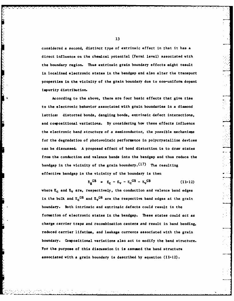
According to the above, there are four basic effects that give rise
to the electronic behavior associated with grain boundaries in a diamond
lattice: distorted bonds, dangling bonds, extrinsic defect interactions,
and compositional variations. By considering how these effects influence
the electronic band structure of a semiconductor, the possible mechanisms
for the degradation of photovoltaic performance in polycrystalline devices
can be discussed. A proposed effect of bond distortion is to draw states
from the conduction and valence bands into the bandgap and thus reduce the
bandgap in the vicinity of the grain boundary.(1 7) The resulting
effective bandgap in the vicinity of the boundary is then
EgGB . Ec - Ev - EcGB - EvGB (11-12)
where Ec and Ev are, respectively, the conduction and valence band edges
in the bulk and ECOB and EvGB are the respective band edges at the grain
boundary. Both intrinsic and extrinsic defects could result in the
formation of electronic states in the bandgap. These states could act as
charge carrier traps and recombination centers and result in band bending,
reduced carrier lifetime, and leakage currents associated with the grain
boundary. Compositional variations also act to modify the band structure.
For the purpose of this discussion it is assumed the band structure
associated with a grain boundary is described by equation (11-12).
14
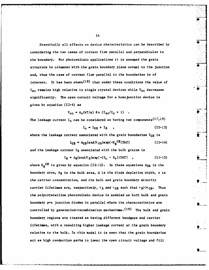
Essentially all effects on device characteristics can be described by "
considering the two cases of current flow parallel and perpendicular to
the boundary. For photovoltaic applications it is assumed the grain
structure is columnar with the grain boundary plane normal to the Junction
and, thus the case of current flow parallel to the boundaries is of
interest. It has been shown(1 8) that under these conditions the value of
Isc remains high relative to single crystal devices while Voc decreases "
significantly. The open curcuit voltage for a homojunction device is
given by equation (11-4) as
Voc - Ao(kT/e) In (Isc/Io + 1)
The leakage current 1o can be considered as having two components(1 7,19 )
Io IGB + IB (11-13)
where the leakage current associated with the grain boundaries IGB is
IGB = AGB(end/rGB)exp(-EgGB/2kT) (11-14)
and the leakage current Ij associated with the bulk grains is
IB - AB(end/rB)exp(-(Ec - Ev)/2kT] , (11-15)
where EgGB is given by equation (11-12). In these equations AGB is the
boundary area, AB is the bulk area, d is the diode depletion width, n is
the carrier concentration, and the bulk and grain boundary minority
carrier lifetimes are, respectively, T B and TGB such that TB>FGB. Thus
the polycrystalline photovoltaic device is modeled as both bulk and grain
boundary p-n Junction diodes in parallel where the characteristics are
controlled by generation-recombination mechanisms.( 19 ) The bulk and grain
boundary regions are treated as having different bandgaps and carrier
lifetimes, with a resulting higher leakage current at the grain boundary
relative to the bulk. In this model it is seen that the grain boundaries
act as high conduction paths to lower the open circuit voltage and fill
rI

15
factor of the device. This is consistent with the observed performance of
polycrystalline GaAs solar cells.
The second case to consider is current flow perpendicular to the
grain boundary. Band bending at the boundary results in a potential
barrier and, therefore, majority carrier transport perpendicular to the
boundary encounters high resistance. This effect is of consequence in
photovoltaic device applications because it can increase series resistance
and, therefore, reduce Iec and FF. This aspect of current transport will
not be discussed here. It will, however, be discussed in detail in
Chapter 3 as it pertains to the analysis of the electronic properties of
semiconductor grain boundaries. In addition, the properties of majority
carrier transport across grain boundaries will be used later in this
thesis to study the relationship between grain boundary structure and
electronic behavior. This transport mechanism is dominant in
polycrystalline materials that display varistor behavior.
Based on this discussion of the possible origins of the electronic
behavior of grain boundaries, various schemes for the passivation of grain
boundaries in photovoltaic devices can be presented. In order to
eliminate trap states that could restilt from dangling bands, it may be
possible to introduce impurities that would bond at these sites. Such an
effect has been demonstrated by the improvement in performance of
polycrystalline Si photovoltaic devices after annealing in atomic
hydrogen.(2 0,2 1) Such a passivation mechanism has not been observed in
polycrystalline GaAs. The effects of distorted bonds at the grain
boundary might be eliminated by substitution of atoms that form stronger
or weaker bonds with the host lattice atoms at the boundary plane. The
high leakage current associated with grain boundaries might be reduced by

16
increasing the resistivity along the boundary. It has been shown that Voc
can be increased in GaAs photovoltaics by insulating high leakage
boundaries with an anodic oxide cap.(22) Intrinsic and extrinsic effects
might be reduced, respectively, by introducing preferential grain
orientations having boundaries with structures and kinetic properties that
have minimal effect on device performance.
2.4 Summary
This chapter describes the effects of grain boundaries on
photovoltaic device performance by presenting the basic principles of
operation of a photovoltaic device, the electronic energy band structure
associated with grain boundaries, and the effect of this band structure on
device operating parameters. An understanding of the parameters
describing photovoltaic device performance will be necessary for
discussing some of the experimental results that are presented later.

17
3: Literature Review
3.1 Electronic Properties of Grain Boundaries in Semiconductors
The electronic behavior of grain boundaries in semiconductors has
been studied since about 1950. The early work covered in the first twenty
years dealt primarily with grain boundaries in Ge. In the early 1970's
the emphasis shifted to the study of grain boundaries in Si, the primary
motivation arising from the application of polycrystalline Si for solar
cells and conducting layers for integrated circuits. This section is a
review of the available, pertinent literature on the electronic properties
of semiconductor grain boundaries. The order of discussion is such thatL
the properties of grain boundaries in Ge will be presented first followed
by Si and GaAs. A few other material systems will be briefly mentioned.
Although partitioned by subject, this will essentially be a chronological --
presentation.
3.1.1 Grain Boundaries in Germanium
The first published observations of the electrical properties of
semiconductor grain boundaries were presented by Pearson.(2 3) He observed
that carrier transport across a grain boundary in n-type Ge was consistent
with a back-to-back Schottky diode behavior. He showed that this behavior
is consistent with acceptor states located at the grain boundary plane
which can be represented as a a-p-n semiconductor structure. Pearson
attributed the occurrence of these grain boundary states to misfit between
the lattices of the two joining crystals. It was also shown that the
potential barrier associated with the grain boundary and giving rise to
the transport characteristics could be eliminated by converting the
material to p-type by heat treatment. The work of Taylor, Odell, and

18
Fan(2 4) in 1952 was the first detailed publication of the carrier
transport across Ge grain boundaries. It presented a quantitative
analysis of electrical transport properties to determine the electronic
nature of grain boundaries in Ge bicrystals. Their analysis was based on
current-voltage (I-V) and capacitance-voltage (C-V) measurements. They
also observed the back-to-back diode characteristic for n-type Ge and
found no barrier in p-type Ge. The I-V characteristics of the n-type
material showed an asymmetry with respect to the bias polarity of the
grains. The C-V measurements confirmed that this was due to different
carrier concentrations in each grain of their bicrystal samples. The C-V
data also provided a measure of the extent of band bending associated with
the Ge grain boundaries. The room temperature barrier height for highly
rectifying grain boundaries was determined to be about 0.4 eV for carrier
concentrations in the mid 1014 cm -3 range.
The breakdown voltage associated with the back-to-back diode formed
by the grain boundary was attributed to the complete filling of the
electronic states in the grain boundary. From this assumption the maximum
number of grain boundary states was calculated to be on the order of 1012
cm- 2 of grain boundary area. The authors attribute the possible origin of
the electronic states to lattice misfit and/or segregation of acceptor
impurities at the grain boundary.
It was apparent that the bonding structure at the boundary interface
and impurity effects may both influence the electronic behavior of grain
boundaries in semiconductors. The research conducted in this area until
the early 1960's was directed toward an understanding of these effects.
In 1953 Shockley( 16 ) proposed that the acceptor states localized at
Ge grain boundaries were intrinsic in origin. He proposed that

19
"edge-states" analogous to surface states(2 5) exist at the grain boundary
and are associated with partially filled (dangling) bonding orbitals.
Assuming the grain boundary consists of a dislocation array,(5) Shockley
proposed that these edge-states are associated with the edge components of
the dislocations forming the boundary structure. Besides generating a
large barrier to transport across the boundary, this electronic structure
would result in an abnormlly high conductivity in the grain boundary
plane itself. This effect was indeed shown to exist by Tweet.(2 6,2 7)
The work by Tweet(2 6,2 7) is the first reported study on the electronic
properties of grain boundaries in Ge bicrystals with controlled L
orientations. These bicrystals were grown from the melt and had a
predetermined angle of tilt about the [1101 or [1001, although the boundary
plane itself was not controlled. In this work Tweet investigated carrier
transport properties in the grain boundary plane. Although he did vary the
tilt angle between 5 and 15*, the most significant results were obtained
from experiments on both n- and p-type bicrystals with a misorientation
angle of 10. His results shed light on both the nature of the grain
boundary states and the influence of boundary structure on the properties
of the grain boundary.
Although it was clear from previous investigations that grain boundary
potential barriers existed in n-type but not in p-type Ge, Tweet's Hall
effect data show that acceptor states are indeed present in grain
boundaries of both material types. He also showed that the resistivity of
the grain boundary was strongly affected by the plane orientation even
though the misorientation angle was held constant. From these measurements
he deduced that these different boundary structures contained different
densities of trapped charge.
i _ L

20
Tweet's transport measurements as a function of temperature indicated
that the conductivity of grain boundaries was constant while that of the
bulk regions behaved in accordance with the accepted semiconductor
statistics. At low temperatures (< 100*K) the conductivity of the
boundaries became the dominant component of conductance measurements made
parallel to the boundary plane. This agreed well with the model proposed
by Shockley.(16) In additon, Tweet observed that twin boundaries did not
show enhanced conductivity. This finding was consistent with the Shockley
model in that there are no dangling bonds associated with the twin
boundary structure and, therefore, no edge-states.
These results established that acceptor states are localized at grain
boundaries in both n- and p-type Ge. The capture of free electrons by
these states results in band bending at boundaries in n-type material and
in a potential barrier. However, it was still uncertain whether these
acceptor states are due to the intrinsic defect structure or due to
impurity segregation (extrinsic effect).
In the short period from 1959 to 1961 several publications indicate
that intrinsic defect states dominate the electronic properties of grain
boundaries in low-doped (< 1016 cm- 3 ) Ge. Reed, Weineich, and Matare(28 )
studied melt grown bicrystals with symmetric tilt boundaries and
misorientation angles ranging from 10 to 30* about the (0101 direction.
Although they did not report effects of varying grain boundary structure,
their results confirm those of Tweet.(2 7 ) They observed the same
temperature independent conductivity in the boundary plane which was found
to exist throughout the temperature range of 2 to 300*K. Since the
acceptor states associated with the grain boundary were found to exist at
temperatures below which carrier freeze-out generally occurs, it is fairly

21
certain that the grain boundary states arise from intrinsic bonding
effects. The authors discuss their data in terms of a dislocation array
model for the boundary structure.
Mueller(2 9) studied carrier transport both across and along symmetric
<100> tilt boundaries in melt-grown Ge bicrystals with misorientation
angles of 4, 6, and 25*. The transport properties were consistent with
those observed by the other workers. However, Mueller did investigate the
effect of boundary structure on electronic properties. He reports the
value of an experimentally determined parameter which is referred to as
electron "capture rate" for the three boundary structures. His findings
are that the capture rate increases non-linearly with the misorientation
angle. The electron capture is attributed by him to dislocation states at
the boundary. This appears to have been the first investigation of the
influence of defect structure on the electronic properties of
semiconductor grain boundaries using predetermined boundary structures.
Matare(3 0) studied transport across tilt boundaries in n-type Ge -
assuming a dislocation model for the boundary structure. He contends that
electrons are trapped by dangling bonds at the edge dislocation cores to
produce a one-dimensional conducting "pipe", as previously proposed by
Shockley.(16) This model is proposed to explain the temperature
independent conductivity in the boundary plane discussed previously.(2 8)
It is also stated that the dangling bond wavefunctions overlap only for
misorientation angles greater than 10. This indicates that there should
be an asymmetry in the transport characteristics for conduction in the
plane of a sufficiently low angle grain boundary. Indeed, this effect was
reported by Matukura and Tanaka(3 1) using melt-grown Ge bicrystals with
symmetric [0101 tilt boundaries. They measured carrier mobility in the
--

22
boundary plane both parallel and perpendicular to the (0101 tilt axis for
samples with 2.5 and 20* misorientation angles. It was found that for a
2.5* misorientation the mobility measured parallel to the tilt axis was
significantly higher than the value perpendicular to the axis. However,
this asymmetry was not observed in the 20" tilt boundary. These results
suggest that a tilt boundary with a sufficiently low misorientation angle
has an anisotropic defect structure, as would be consistent with the
dislocation array model.
Mueller has presented a theoretical(3 2) and experimental(3 3) analysis
of transport across tilt boundaries in n-type Ge. His analysis is also
based on the assuaption of electron trapping by dangling bonds at edge
dislocation cores. The experimental studies were performed on melt-grown ..
n-type bicrystals with symmetric [1001 tilt boundaries with
misorientations of 4, 6, and 25, as in his previous work(29). However,
in this case a [100] twist boundary with a 6* misorientation was also
studied. The tilt boundary data indicate that the grain boundary
potential barrier increases with increasing misorientation angle, as would
be expected from his previous results.(2 9) However, it was found that
both the 60 tilt and twist boundaries exhibited the same electrical
properties. This is significant since the dislocation model for a tilt
boundary consists of pure screw dislocations and, thus, this boundary
structure should have no dangling bonds. Thus it appears that, although a
2.5* [1001 tilt boundary may have a dislocation structure, this model may
no longer be valid for misorientation angles of less than 6. It appears
that as the misorientation angle is increased there is a gradual
transition from a dislocation array structure to a bonding arrangement
more characteristic of clean surfaces.(34)

23
Recent work(3 5) on the electronic properties of tilt boundaries
focused on a [1i01 tilt boundary with a 3.5* misorientation angle and a
(111) boundary plane in Ge. The sample studied was n-type with a carrier
concentration of 2 x 101 3 cm-3. Using deep level transient spectroscopy
(DLTS), a technique described in Appendix 1, a single electron trap level
located in the bandgap at 0.42 eV below the conduction band edge was found
to be associated with the grain boundary. The trap pinned the Fermi levcl
and resulted in a grain boundary barrier with a height of 0.2 eV. This
suggests an explanation for the observation that barriers exist only in
n-type material; the trap state observed is an electron trap and
therefore can only result in a barrier to majority carrier transport in
n-type material.
In summary, the earliest work on the electronic behavior of
semiconductor grain boundaries was limited to the study of Ge. It was
established that the grain boundary interface behaves as if it contains
acceptor-like electronic states in the bandgap which give rise to band
bending in such a fashion as to create a barrier to majority-carrier
transport across a grain boundary in n-type Ge. These states also create
a hole-like conductivity in the boundary plane that is independent of
temperature. These results suggest that the acceptor nature is due, at
least in part, to intrinsic bonding defects at the grain boudary
interface. The structure of the boundary was shown to influence the grain
boundary properties. There is some evidence that the bonding structure of
the grain boundaries is itself determined by the extent of crystallite
misorientation.
_____ i

24
3.1.2 Grain Boundaries in Silicon
In contrast to the extensive work on oriented Ge bicrystals discussed
in the preceeding section, there is only one published investigation of
the properties of Si grain boundaries with knovn structures.(3 6) In this
1961 publication, Matukura investigated the electronic properties of (0101
symmetric tilt boundaries with misorientation angles of 20 and 470 in
p-type Si. The experiments are analogous to those performed by this same
group in n-type Ge.( 3 l) In contrast to the observations in Ge, the grain
boundaries in Si were found to contain donor-like states and, thus, to
have an n-type character. Therefore, the Si grain boundary also has a
back-to-back diode characteristic but is represented as a p-n-p
structure.
No further pertinent studies on the electronic properties of
semiconductor grain boundaries are reported in the open literature until
the 1970s. Investigating majority carrier transport in thin-film
polycrystalline n-type Si, Kains(3 7 ) showed that there are acceptor-like
grain boundary states in Si which result in bending of the electronic
energy bands and in an n-p-n structure analogous to that for Ce. The
observation that potential barriers in Si exist in both n- and p-type
material while in Ge only in n-type material is extremely important; it
suggests that both electron and hole traps are localized at grain
boundaries in Si whereas only electron traps exist at Ge boundaries.
Assuming a constant density of acceptor states in the bandgap, Card
and Yang(3 8) modeled the electrical properties of grain boundaries in
n-type Si and showed how these defects affect the characteristics of
electronic devices fabricated in polycrystalline Si. Although they were
able to show that enhanced carrier recombination at the boundary states

25
could lead to a reduction in both Voc and Isc for solar cells, they
emphasized the necessity of knowing the dependence of the bandgap state
density on the grain boundary structure as an aid in developing
polycrystalline semiconductors for device applications.
The most detailed examination of the electronic structure and
transport properties associated with Si grain boundaries has been
presented in several papers by the Sandia group.(39-4 4) The material
studied by this group was polycrystalline Si prepared by chemical vapor
deposition (CVD) and doped n-type with phosphorous by neutron
transmutation. This doping procedure was employed so that uniform carrier
concentration could be obtained without the need for high temperature
processing that could result in a preferential redistribution of the
dopant at or along the grain boundaries. The first(3 9) in this series of
papers showed results indicating that the heights of the potential
barriers associated with the grain boundaries in randomly oriented
polycrystalline Si ranged from about 0 to 0.5 eV. Because the effects of
impurity redistribution on grain boundary properties are minimal in the
material studied, this investigation provides evidence that the electronic
properties of grain boundaries in Si are strongly influenced by the
boundary structure. Analysing the I-V characteristics for transport
across isolated, highly rectifying boundaries, it was shown that the grain
boundary states are located at the middle of the bandgap. Assuming that
these states can act as either donors or acceptors provides an explanation
for the approximately equal maximum barrier heights observed in both p-and
n-type Si.
Studying the thermal emission of charge from the grain boundary
states,(4 0) it was shown that the maximum density of electron traps
26
associated with highly rectifying Si grain boundaries is about 1012 cm-2.
From detailed studies of the I-V and C-V characteristics of the grain
boundaries,(4 1,4 2) it was concluded that transport across the potential
barrier proceeds by thermionic emission for carrier concentrations up to
approximately 1017 cm 3. Their data suggest further that a single band of
traps centered around the middle of the bandgap and having an
exponentially decreasing density with energy is associated with grain L
boundaries in n-type Si. For rectifying grain boundaries these states are
only partially filled at equilibrium. When a bias voltage is applied such
that essentially all the states are filled the barrier collapses and the
thermionic current increases exponentially. This breakdown of the barrier
is responsible for the back-to-back diode characteristic of the grain
boundary. This particular breakdown is slower and occurs at voltages 5 to j710 times less than the avalanche breakdown of a conventional Si
diode.(4 2)
The applicability of this model to grain boundaries in p-type Si has
been experimentally verified by Martinez, Criado, and Piqueras(4 5) who
observed barrier heights and trap densities that are essentially equal to
those reported for n-type Si by the Sandia group. Their work furthermore
indicates that the electronic properties of a grain boundary can vary
significantly along its length and that the bandgap state density at the
point of intersection of several boundaries appears extremely large. From
their experiments it is difficult to determine if this effect is intrinsic
(structure) or extrinsic.
A qualitative relationship between boundary structure and electronic
properties has been demonstrated in several investigations.(4 6-5 1) These
studies show that grain boundaries in the same sample of polycrystalline
a--
-. -- _____ ___!

27
Si can display properties that are quite different from one boundary to
another. Studies of the performance of solar cells fabricated from
polycrystalline Si( 4 6,4 8) have shown that not all grain boundaries are
"active" in the sense of degrading the performance of photovoltaic
devices. Specifically, it was shown that coherent twin boundaries are
electrically inactive. (46,48)
Helmreich and Seiter(4 7) compared the performance of photovoltaic
devices fabricated from polycrystalline Si prepared by various techniques.
These materials differed from one another with respect to both
microstructure and degree of purity. Their results indicate that both
boundary structure and composition influence the electronic properties of
the grain boundaries. Cheng and Shyu(49) showed that both the potential
barrier and bandgap states associated with a multifaceted grain boundary
in p-type Si vary not only from facet to facet but also along the length
of a single facet. This also suggests an influence of both structure and
composition on grain boundary properties. Wu and Yang(5 0) have attempted
to model the effect of these property variations on the thermnionic current
flow across semiconductor grain boundaries.
Redfield(5 1) recently observed a direct relationship between oxygen
redistribution and the electrical activity of grain boundaries in both
n- and p-type cast polycrystalline Si. The grain boundaries in this
material were observed to be inactive when there was a uniform
distribution of oxygen measured in the grains. Upon heat treatment the
oxygen was redistributed to yield oxide precipitates in the grains and
regions denuded of oxygen adjacent to grain boundaries. Measurement of
the electronic properties after the heat treatment showed that the grain
boundaries were electrically active. Measurements by Kazmerski(5 2) in

28
p-type Si show that segregation of oxygen in grain boundaries during heat
treatment results in an increased grain boundary potential barrier and in
a decreased minority carrier lifetime in the vicinity of a boundary.
Grain boundary segregation of Al and Ti during solidification is also
shown to result in an increased barrier height and a decrease in minority
carrier lifetime.
It is clear from these investigations that oxygen, and other
impurities, influence the electronic properties of grain boundaries in Si,
although the nature of this effect is uncertain. For instance, oxygen may
be the direct cause of the grain boundary activity after heat treatment.
On the other hand, before heat treatment the oxygen may be present at the
grain boundary in such a way as to eliminate the grain boundary states.
Heat treatment could then cause this bonding configuration to be disrupted
with the oxygen going to precipitate or compound formation.
Leamy et al.(5 3) investigated the effect of grain boundaries on the
performance of transistors fabricated in polycrystalline Si. They also
observed variations in the heights of potential barriers associated with
different grain boundaries. Twin boundaries showed no effect on device
performance. Impurity diffusion, employed for device fabrication, was
clearly enhanced along many of the grain boundaries. The diffusion
coefficient for As along grain boundaries in Si was calculated to be on
the order of 10- 11 cm2/sec. The diffusion coefficient for As in bulk Si
is about 10- 15 cm2/sec at 100oC.(3)
Grain boundary potential barriers exist in both n- and p-type Si, in
contrast to the case of Ge. This may be due to pinning of the Fermi level
by the grain boundary states at different positions or the ability of
these states to act as both electron and hole traps for these materials.

29
It is of interest to note that, unlike the studies of grain boundaries in
Ge, there were few studies of the properties of Si grain boundaries having
known structures. This is suprising because of the observed influence of
structure on grain boundary properties. Detailed transport studies have
shown how grain boundary states give rise to the back-to-back diode
characteristic for thermionic current flow across a grain boundary. Not
all grain boundaries in Si are electrically active. This is influenced by
both the intrinsic grain boundary structure and extrinsic, probably
compositional, effects. Enhanced impurity diffusion along grain
boundaries was also observed.
3.1.3 Grain Boundaries in Gallium Arsenide
The study of the electronic behavior of grain boundaries in GaAs and
related Il-V compounds has not been addressed to nearly the same extent
as the studies in Ge and Si. This subject has only been treated in the
literature since the late 1970s. However, there are some general trends
that can be observed from these investigations and these will be presented
in this section.
In contrast to the studies with Ge and Si bicrystals, most of the
early investigations of the electronic properties of GaAs were based on
indirect electrical measurements using Schottky diodes on polycrystalline
samples.(5 4,5 7) In a study of n-type polycrystalline GaAs prepared by CVD,
Hwang, Card, and Yang(5 4) found that the charge at the grain boundary core
was positive indicating that the associated bandgap states are
acceptor-like. Yang et al.(55) studied both n- and p-type CVD
polycrystalline GaAs. Their results are consistent with the
double-depletion-region model and indicate a significantly higher

30
potential barrier for grain boundaries in r-type than in p-type GaAs.
They found that the number of filled grain boundary states at equilibrium
is a function of donor density. This effect was attributed by them to a
continuous distribution of bandgap states. The model proposed to explain
their results calls for a distribution of bandgap states having a minimum
at 0.75eV below the conduction band edge and increasing towards the band
edges. States above the minimum are acceptor-like and those below are "
donor-like. An alternative model was proposed by Fan et al.(58,5 9) based
on studies of laser beam annealing of GaAs and InP. This model is based
on Fermi level pinning at all types of crystal defects in a fashion P
similar to that for surfaces. Their measurements on both n- and p-type
GaAs and InP are consistent with this model.
Cohen et al.(5 6,6 0) studied the properties of grain boundaries in P
n-type GaAs epitaxial layers grown on polycrystalline GaAs substrates.
They measured both the resistance of individual grain boundaries and the
properties of Schottky diodes on the material. They reported, consistent p
with the double-depletion-region model, that individual grain boundaries
could be highly rectifying, with measured barrier heights of 1.1eV for a
carrier concentration of 2 x 1015 cm-3. Their Schottky diode
characteristics indicate that the grain boundaries act as high leakage
paths and that the leakage increases with carrier concentration. This was
attributed to electron tunneling through the grain boundary barrier to the -
bandgap states. Charge carriers in the bandgap states have an enhanced
mobility in the boundary plane and are responsible for the observed
leakage current. This concept is supported by the recent experimental
observation of electron tunneling through grain boundary potential
barriers in highly doped GaAs.( 6 1) Kazmerski and Ireland( 57) found that

31
this leakage current is reduced by the segregation of oxygen to the grain
boundaries during epitaxial growth. The oxygen is believed to be present
in the form of Ga2 03. In this case impurity segregation to the grain
boundaries was found to improve device performance.
Spencer et al.(6 2,6 3) studied the electronic states associated with a
grain boundary in an epitaxial n-type GaAs layer on a polycrystalline
substrate using DLTS. This technique enables direct measurement of the
nature of the bandgap states. In contrast to the electronic state model
proposed by Yang et al.(5 5), it was found that the dominant grain boundary
states are discrete levels. Two majority carrier traps were found at 0.62 L
and 0.74 eV below the conduction band edge. In addition, several other
levels were detected that were attributed to either trap states in the
grains or to impurities. The source of the impurities was suspected to be
the substrate. There was no attempt to relate these results to the grain
boundary structure.
McPherson et al.(6 4) developed a theoretical model for the electronic
properties of symmetric tilt boundaries in GaAs assuming a simple
dislocation structure for the boundaries. They predict a decrease in
barrier height with increasing misorientation angle for values greater
than 1. This is due to a decrease in the predicted probability of
occupancy of the grain boundary states, which are attributed to dangling
bonds at the dislocation cores, as the misorientation angle is increased.
This effect can be viewed as arising due to "electron screening" by
localized charge at closely spaced dangling bonds. Their theory also
predicts a decrease in the potential barrier with increasing donor
density.
In a subsequent study,(6 5) this group measured the characteristics for

32
majority carrier transport across randomly oriented grain boundaries in
melt-grown, n-type GaAs. They found that grain boundaries with a widely
spaced dislocation structure, as determined by etch pit measurements,
showed no substantial associated potential barrier. Other boundaries, for
which a distinct dislocation structure could not be resolved, showed
varying degrees of rectification indicating a range of potential barriers.
The maximum room temperature barrier heights measured by them were about
1.0 eV. The barrier height was found to decrease rapidly as the carrier
concentration is increased. The observed transport properties were found
to give a reasonable fit to a model using the defect levels identified by
DLTS.(6 2) This model indicated acceptor-like state densities of 5.2 x
1011 cm- 2 at Ec - 0.41 eV and 9.0 x 1011 cm- 2 at Ec - 0.9 eV. It must be
pointed out that other bulk states had to be included to get a reasonable
fit. It is also noteworthy that the maximum measured density of grain
boundary states of approximately 1012 cm-2 for the highly rectifying
samples is lower than that indicated by their theoretical analysis( 6 4 )
assufing a simple dislocation array boundary structure.
A study of grain boundaries in the related III-V compound
semiconductor GaP(6 6) showed results that are qualitatively similar to
those obtained for GaAs. It was found that the height of the grain
boundary potential barrier in n-type GaP is approximately twice that in
p-type materiaL This is reportedly the same situation that occurs for
Schottky barriers on GaP with high interface state densities. The same
study suggests that twin boundaries show no associated potential barrier.
However, no further attempt was made to relate the grain boundary
structure and properties.
Grain boundary potential barriers have been shown to exist in both

33
n-type and p-type GaAs. The barrier in p-type GaAs, however, is
significantly lower than in n-type material. There have been two
models(5 5,6 3) proposed for the structure of electronic bandgap states
associated with the grain boundaries. These are schematically presented
in figure 3-1. Also included in this figure is the bandgap state model
that will be presented on the basis of this thesis work and is consistent
with Fan's model. (58,59) This model consists of two bands of states
located at 0.65 eV and 0.9 eV below the conduction band edge. The study
of grain boundaries in GaP indicates a connection between grain boundary
states and other types of interface states. The model proposed in this
thesis for the grain boundary states in GaAs will be shown to be
consistent with a unified model for GaAs interface states.
The influence of impurities on GaAs grain boundary properties has
been demonstrated. A model for the electronic properties of GaAs tilt
boundaries as a function of misorientation angle based on a simple
dislocation array model for the boundary structure has been reviewed.
(The influence of both impurities and structure on the electronic
properties of GaAs grain boundaries will be discussed in depth in the
following chapters.)
3.2 Chemical Modification of Grain Boundary Properties
The influence of chemical impurities on the properties of
semiconductor grain boundaries has been indicated in the previous sections
of this chapter. This section will summarize some of these effects and,
in addition, discuss the intentional modification of grain boundary
properties by the introduction of preselected chemical species into the
boundary region.
The effect of oxygen on the electronic properties of grain boundaries

34
0 E4
0.2-
0.4 /Y*- ANG ET AL.SPENCER ET AL.
/ --- T HIS WORK
570.6 j.-
S0.8
1.0
1.2-
1.4E,
NT
Fig. 3-1. Schematic illustration of proposedmodels for grain boundary states in GaAs. _

35
in st(5 1, 5 2) and GaAs(5 7) has been discussed previously. The oxygen was
present in the as-grown material and its distribution was found to be a
function of the processing treatment.( 5 1) It is not clear from the work
reported if the bonding configuration of the oxygen at the grain
boundaries is important in determining its effect on properties or if the
mere presence of oxygen in any configuration is responsible. These are key
issues for which available data is insufficient. It was also found that
other impurities that preferentially segregate to Si grain boundaries
during growth have a significant effect on the observed electronic
properties of the defects.(5 2) These results indicate that the properties
of grain boundaries in polycrystalline semiconductors are influenced by
composition. Since the distrubution of the impurities in the material is
a function of the thermal history of the material, it is important to
realize that the observed grain boundary properties may be influenced by
the sample preparation technique.
In addition to the compositional effects in the as-grown materials,
the intentional selective chemical modification of the grain boundaries
has been demonstrated to affect the grain boundary properties. The
studies cited in this section discuss the spatially selective introduction
of impurities into the grain boundaries in an effort to eliminate the
deleterious effects of the boundaries on device performance by eliminating
the bandgap states. This is refered to as grain boundary passivation.
The most convincing evidence that the electronic states associated
with grain boundaries can be eliminated by chemical modification is found
in work on the introduction of atomic hydrogen into both n- and p-type Si
grain boundaries.(2 0,2 1,4 8,6 7- 70) This process is assumed to involve the
preferential grain boundary diffusion of ionized hydrogen. Lam (71) has

36
shown that similar effects can be achieved by exposing polycrystalline Si
to molecular hydrogen. The results indicate that the hydrogen acts to
reduce the density of grain boundary states in the bandgap with a
corresponding reduction in the height of the associated potential barrier.
This passivation has been demonstrated by examining both the properties of
individual grain boundaries and the performance of polycrystalline solar
cells.
The role of hydrogen has been clearly demonstrated by its removal
from the passivated Si through annealing in a hydrogen-free ambient and
the subsequent return to the original grain boundary properties. This
effect has been demonstrated to occur over several of these cycles. The
mechanism of hydrogen passivation of Si grain boundary states is not
clear. The hydrogen may attach itself to dangling bonds at the grain
boundary cores or act to reduce Si-O bonds at the grain boundary that are
responsible for the bandgap states.
Hydrogen has not been shown to be effective for the passivation of
grain boundary states in GaAs or other Ill-V compounds. There is good
evidence that preferential diffusion of Sn into grain boundaries in n-type
GaAs acts to compensate the acceptor-like grain boundary states.( 7 2 ) This
Sn passivation process appears to improve the performance of
polycrystalline GaAs p-n junction solar cells.(7 3) In a similar approach
to passivation of GaAs grain boundaries by compensation, potassium was
diffused into a bicrystal sample(6 5) and the height of the associated
potential barrier was found to be lowered. Nitrogen diffused along grain
boundaries in polycrystalline InP has been shown to improve the
performance of solar cells fabricated from this material.(7 4) These
studies clearly show that the electronic properties of grain boundaries in
A---

.',. . . . .. .I . .-
37
III-V semiconductors can be improved by chemical modification. However,
it is not clear that this improvement results directly from the
elimination of intrinsic grain boundary states*
In summary, the electronic properties of grain boundaries in
semiconductors can be altered by chemical modification. In the case of
Si, hydrogen treatment can lead to grain boundary passivation by the
direct elimination of bandgap states. The mechanism for this effect is
not clear. Various treatments have been demonstrated to influence the
properties of grain boundaries in III-V semiconductors, however there is
no direct evidence for the elimination of the grain boundary states inL
these materials.
3.3 Physical Properties of Grain Boundaries
The following sections discuss the physical nature of grain
boundaries. First, an introduction to grain boundary structure and the
influence of the structure on impurity segregation will be presented based
on a few general references. This will provide the concepts and
terminology needed for later discussions. Following this is a discussion
of the structure of grain boundaries specific to covalently bonded
semiconductors. This is based on recent experimental studies of grain
boundaries in Ge and Si. It will be shown that the structure of grain
boundaries in these materials is significantly more complex than that
suggested by the simplified models. It will be obvious, however, that
there is a periodic structure that is associated with grain boundaries in
semiconductors. This is an important concept in that it can be
interpreted as the result of reconstructed bonding at the grain boundary
interface.

38
3.3.1 Grain Boundary Structure and Segregation
Presented here is a general discussion of the structure of grain
boundaries and the relation between grain boundary structure and
segregation. A grain boundary is the planar interface between two
crystallites (grains) of the same material whose lattices are misoriented
with respect to each other. There are nine parameters that define the
structure of a grain boundary.(7 5) The misorientation of the two lattices
is defined by the angles of rotation about any three unique rotation axes.
In addition to these six parameters, the grain boundary plane is defined
by three coordinates. These parameters are usually referenced to the -
coordinate system that defines the unit cell of one of the lattices. On
one side of the grain boundary plane atoms occupy sites of only one of the
lattices while on the other side of this plane only sites of the other
lattice are occupied.
There are two special cases that arise when the grain boundary
structure is given by a rotation of the lattices about a single axis. " -
These structures are defined by the single rotation axis, a single
rotation angle, denoted as e, and the three coordinates defining the
boundary plane. If the rotation axis is parallel to the boundary plane
the structure is called a tilt boundary. The second special case is the
twist boundary, for which the boundary plane is perpendicular to the
rotation axis. If the boundary plane bisects the tilt angle, the
structure is termed a symmetric tilt boundary. For the purposes of the
discussions of this thesis, boundary structures that can be viewed as
rotations about a single axis will be denoted by the rotation angle, the
rotation axis, and the boundary plane given in the coordinate frame
of one of the lattices. For example, a tilt boundary lying in the (T11)

39
plane and having a misorientation angle 0 = 100 about the [110] direction
is denoted as 10"[110]/(T1I). This notation convention provides no
indication of whether or not a structure is symmetric.
The basic models for grain boundary structure propose that the misfit
that results from the misorientation of the two lattices is accomodated by
the generation of dislocation arrays in the boundary plane.( 75- 78 ) Since a
general grain boundary is characterized by rotations about three axes,
such a boundary has three associated dislocation arrays having different
and non-coplanar Burgers vectors. The dislocations which occur at these
general boundaries can have both screw and edge components. However, tilt
and twist boundaries contain only pure edge and pure screw dislocations,
respectively.
The spacing between the grain boundary dislocations, for a symmetric
boundary, is given by(75)
d " b I ,(I -)
2sin(0/2)
where b is the Burgers vector of the appropriate lattice dislocation. The
spacing between dislocations decreases as the misorientation angle is
increased. Above some critical misorientation angle, Gc, the spacing
between dislocations is sufficiently small that the grain boundary
structure can no longer be considered to be composed of individual lattice
dislocations. Grain boundaries with tisorientations significantly below
this critical angle are termed "low angle," those with misorientations in
the range of ec are termed "medium angle," and those with misorientation
angles significantly greater than Oc are termed "high angle." The
critical misorientation angle is generally considered to be in the
vicinity of 15.
.- .- . .

p..
40
U The microstructure of low angle grain boundaries can be adequately
described by arrays of dislocations, termed grain boundary dislocations
(GBDs), formed in the crystallographic lattice appropriate for the
particular material composing the grains. However, the validity of this
model becomes questionable as the misorientation angle approaches the
value of Oc . In this limit the structure can no longer be assumed to be
based on discrete GBDs and it becomes necessary to adopt other formalisms
to describe the unique "crystallography" associated with a grain
boundary.(7 9) In contrast to the limited applicability of the GBD model,
this grain boundary crystallography can be used to describe all grain
boundary structures. The key point of this description is that all grain
boundary structures are periodic to an extent related to the misfit
between the two crystallites. These formalisms and the relation of the
resulting boundary structures to grain boundary segregation will now be
presented. The discussion is derived from a few general
references. (79-81)
When the lattice of one grain is rotated with respect to the lattice
of the other grain there are certain sites of both lattices which remain
in registry. These sites theselves form a lattice, termed the
Coincidence Site Lattice (CSL), that describes the basic periodicity of
the grain boundary structure. Such a rotation gives rise to sets of
points, whose loci are sets of parallel lines, where the fractional
coordinates of the two real lattices are identical. These lines form a
lattice, termed the O-Lattice, which specifies the origin of the
transformation between the lattices of the two grains. The GBDs whose
spacing is given by equation (III-1) are defined by this O-Lattice. There
are three unique displacement vectors that leave the three dimensional

41
structure formed by the rotation of the lattices of the two grains
unchanged. These three vectors define the DSC-Lattice (Displacement Shift
Complete). The magnitudes of these DSC-Lattice basis vectors increase
with increasing degree of coincidence. These three new lattice geometries
provide the mathematical formalism for the description of the periodic
atomic arrangements that form the structure of a grain boundary. Any
further discussion of this theory is beyond the scope of this thesis.
There is another type of grain boundary dislocation that can be
defined in terms of the DSC-Lattice. Because of the nature of the
DSC-Lattice, these secondary grain boundary dislocations (SGBDs) can haveL
discrete spacings that are smaller than the atomic spacings associated
with the lattices of the individual grains. Thus SGBDs can be part of any
grain boundary structure regardless of the magnitude of the misorientation
angle. There are, however, "special" high coincidence boundary
orientations for which the SGBD spacing approaches infinity. The SGBD
spacing is given by4. 4.
ds _bsi - (111-2)d 2sin(Ae/2) s3-0
4.
where AO is the deviation in e from the high coincidence angle and bs is
the appropriate Burgers vector defined in the DSC-Lattice. In general, a
larger spacing between grain boundary dislocations is associated with a
higher degree of periodicity and a lower grain boundary energy. This is
schematically illustrated as a function of misorientation angle in figure
3-2. The spacing between both primary and secondary GBDs is shown as well
as the energy cusps which occur at special high angle grain boundaries.
It is reasonable to expect that most grain boundary properties will
exhibit a functionality with 0 similar to that of the grain boundary

42
SECONDARY
I I I
DISLOCATION I
SPACING I I- !'I \ II IlI \ I\1
PRIMARY
0
GRAIN
BOUNDARYENERGY
IC 0
Fig. 3-2. Schematic illustration of the variationof grain boundary dislocation spacing (top) andenergy (bottom) with misorientation angle.

43
energy
From the above discussion it is clear that grain boundaries are
crystal defects with highly complex structures and, correspondingly, a
variety of atomic sites that will influence their properties. The
implications of this in terms of electronic behavior will be discussed
later. However, the influence of this structure on grain boundary
composition will now be discussed in relation to grain boundary
segregation.
The variety of atomic sites at a grain boundary available to solute
atoms permits a wide range of segregation behavior. It is expected that
segregating species could behave in a simple fashion and adapt to the
basic grain boundary structure or, at the other extreme, segregation could
result in altered atomic arrangements at the grain boundary. Although
impurity distribution at distances much greater than the grain boundary
width can be affected by solute segregation, it has been observed(8 2) that
segregated atoms are localized to a narrow region of approximately 10 A
centered about the grain boundary plane. The lateral distribution of
solute atom along a single grain boundary plane appears to be random.
Several investigations(8 2- 84) indicate that the extent of grain
boundary segregation is related to the boundary structure. It appears
that segregation to special boundaries occurs to a lesser extent than
segregation to boundaries that have a low degree of coincidence. This is
intuitively logical in that the better lattice matching that occurs at
high coincidence boundaries should result in less "void space" in the
boundary region. The degree of segregation to grain boundaries is
considerably less than that to free surfaces. This is expected since
nearly normal lattice density and bonding configurations are preserved at
-a - -. ~ - - - - -. ._

44
a grain boundary, in contrast to the severe structural perturbations
present at a free surface. No systematic studies of the relation between
boundary structure and segregation have as yet been performed. It is
important to point out that the influence of structure on interactionsP
between grain boundaries and other types of crystal defects is probably
similar to the effects observed for solute segregation.
This section bas presented a discussion of the structure of grain
boundaries and the implications of this structure on physical properties.
The formalisms developed to describe the boundary structure are based on a
grain boundary crystallography with an inherent periodic nature of the
atomic arrangements at the boundary. These formalisms result in boundary
structures with a variety of local atomic arrangements that can be
described In term of primary and secondary grain boundary dislocations.
These bonding variations allow a wide range of grain boundary properties,
solute segregation behavior, and other defect interactions.
3.3.2 Grain Boundaries in Semiconductors
This section will discuss the structure of grain boundaries that are
specific to covalently bonded semiconductors having a diamond cubic
structure. Detailed investigations of the structures of such grain
boundaries have been confined to the elemental Ge(85 -91) and Si(92-98)
systeim. The observed structures are similar for the two system and the
results should be generally applicable to lit-V materials. However,
additional restraints on the bonding arrangements in IIt-V Systems will be
shown to complicate the grain boundary structure. The structure of grain
boundaries in semiconductors will be shown to be more complex than those
suggested by the formalisms presented in the previous section. This

45
effect can be interpreted in terms of reconstruction of the local bonding
arrangements. Regardless of the mechanism of its formation, it will be
shown that the structure of grain boundaries in semiconductors is itself
periodic in nature.
Low angle grain boundaries in Ge( 8 6,88) and Si( 9 3-94) have been shown
to be composed of discrete dislocations. This description is valid for
[110] tilt boundaries with misorientation angles of less than 50.(86) For
twist boundaries this model fails for misorientation angles in the range
of 3 to 80.( 9 3) It has been shown that such low angle boundaries can
contain several types of dislocations, the arrangement of which depends on
the misorientation of the two grains.(8 6-9 4) These dislocations can
dissociate into stacking faults bounded by partial dislocations. It has
been proposed that this low angle grain boundary structure, consisting of
different types of dislocations, is a result of interactions between
lattice dislocations.(9 9) The resulting structure is incompatible with
the simple dislocation arrangement given by equation (III-1).
Since the grain boundary structure can be considered to result from
the interaction of lattice dislocations described by equation (Ill-l), it
can be attributed to a reconstruction of the bonding arrangement at the
interface of the two grains. Due to the directional bonding required in
the diamond cubic lattice, the nature of dislocations in semiconductors is
such that reconstruction could result in a grain boundary structure that
does not contain dangling bonds.(6) This bonding reconstruction results
in a periodic arrangement of atoms at low angle grain boundaries that has
been experimental observed by electron diffraction.(9 3)
A change in grain boundary structure that occurs with transition from
the low angle regime to larger misorientations is indicated by the

7
7-7
46
electronic properties of Ge grain boundaries. For example, the
anisotropic nature of transport in the grain boundary plane, indicative of
the presence of discrete dislocations, disappeared as the misorientation
angle increased.(3 1) In another study,(3 3) tilt and twist boundaries,
both having a misorientation angle of 6, displayed the same properties
although their dislocaton structures should be different. This is
consistent with the transition from the low angle regime observed to occur
at approximately 5*.(86,93) The nature of these high angle structures
will now be discussed.
It has been shown that, consistent with the formalisms developed in
the previous section, grain boundaries in covalent semiconductors form
structures to achieve a high degree of coincidence(8 9,9 2,9 7) and can be
described in term of primary and secondary grain boundary
dislocations.(8 9) However, the atomistic structure of the grain boundary
interface is not uniquely specified by the macroscopic structure given by
the rotational misorientation and grain boundary plane.(95,98) It has
been observed that high angle grain boundaries in Ge(9 1) and Si( 9 5,9 7,9 8)
form microfacets, with dimensions on the order of 10 A, leading to grain
boundary plane orientations that contain a high planar density of CSL
sites. This arrangement is achieved by the effective relative translation
of one grain with respect to the other.(9 5,9 7,9 8) Grain boundaries that
facet microscopically and thus achieve a high coincidence site density
have been shown to have such an associated displacement.(9 5 98) There is
no translation associated with coherent twin boundaries(9 8) that have, by
their nature, an exact coincidence structure. The occurance of such
translations can be physically interpreted as the reconstruction of the
bonding arrangements at the grain boundary interface.( 9 8) This bond

47
reconstruction results in the formation of five, six, and seven member
rings at the grain boundary. Some of the bonds contained in these rings
are dilated compared to the bonds in the six member ring structure that
forms a perfect diamond cubic lattice. This bonding configuration has
been observed at grain boundaries in Ge(8 5,9l) and Si.( 9 2,9 5,9 8) A key
feature that results from this reconstructed bonding is that no dangling
bonds occur at the grain boundaries. If bonding reconstruction did not
occur, high angle grain boundaries in diamond cubic semiconductors would
contain a high density of dangling bonds.(9 6)
Thus there is good experimental evidence that reconstructed bonding
occurs at grain boundaries in diamond cubic semiconductors and results in
a structure that contains five, six, and seven member rings with dilated
bonds. These ring structures are arranged in a periodic fashion along the
grain boundary to give rise to the experimentally observed periodic nature
of the boundary structure. The density of these rings in the grain
boundary is directly related to the grain boundary misorientation
parameters.
The only effect of this ring structure in elemental semiconductors is
the dilation of some bonds, with correspondingly induced variations in
bond angle. However, in the II-V system this structure requires the
existance of III-III and V-V bonds. For the case of GaAs, this gives rise
to Ga-Ga and As-As bonds. These bonding defects are analogous to missing
As and Ga atoms, respectively. This type of defect, with only one bond to
a like atom, differs significantly from an antisite defect in a single
crystal, which requires all bonds to be with like atoms. The bandgap
states that result from this type of grain boundary defect must,
therefore, be expected to be different from those that arise in a single

48
crystil. Depending on the stability of such defects, a completely
different bonding arrangement could arise. Thus, the formation of such a
ring structure in Il-V semiconductor grain boundaries results in dilated
bonds, variations in bond angle, and both Ga-Ga and As-As like-atom bonds
(or related defects). Figure 3-3 shows such a structure as proposed for a
microfacet formed along a high order twin plane in Si.( 98 ) When applied
to the 111-V system, as Is shown in the figure, like-atom bonds result.
These like-atom bonds are circled in figure 3-3.
There is good experimental evidence that grain boundaries in
covalently bonded semiconductors have a periodic structure. The atomistic
interface structure is not specified by the macroscopic (geometric)
structure parameters defined by the rotational misorientation and the
grain boundary plane. For small misorientations the structure consists of
discrete dislocations and evolves into a periodic arrangement of five,
six, and seven member rings as the misorientation increases. It is a key
feature of these structural models that grain boundaries need not contain
dangling bonds. The nature of ll-V bonding results in grain boundary
defects that do not occur in the elemental system.
3.4 Summary
This chapter has presented a review of the available literature
pertinent to the electronic, chemical, and physical properties of grain
boundaries in covalent semiconductors. The electronic properties of the
grain boundaries are determined by the nature of the bandgap states.
These states arise due to both the bonding configurations at the grain
boundary interface and compositional effects. The bonding arrangements at
the grain boundary are periodic along the interface and are determined by
4.

077 7--- -
49
GB PLANE
[0011 PROJECTION
10T 1 011)0 Ga (0.0.0)Ol0~" ]• o Ga ('A. 'A, 1/4
(l00J . A As (0,0,0)
[100]" ) &As ('A, , 4)
Fig. 3-3. Possible bonding configuration at a GaAsgrain boundary showing the formation of five andseven member rings.

50
the misorientation relationship between the two grains. Geometrical
formalisms can be used to model the influence of misorientation on the
boundary structure but they do not specify the atomic structure at the
interface. Direct determination of this atomic arrangement indicates the
occurance of a characteristic structure of bonding defects with a planar
density determined by the misorientation relationship. The bandgap states
intrinsic to the grain boundary can most likely be attributed to these
bonding defects.
7-

51 •
4: Experimental Approach
The experimental investigations presented in the following chapters
can be considered to be in two parts. The first deals with the study of
grain boundaries characteristic of polycrystalline, melt-grown GaAs. The
second part is based on a study of bicrystals with preselected grain
boundary structures. It is the purpose of this chapter to discuss the
reasoning that carried this research along this particular path.
The early approach to the problem of studying grain boundary effects
on solar cells involved fabricating many small epitaxial n+/p/p+ mesa
diode cells on a large area melt-grown, polycrystalline GaAs substrate.
Each of the diodes contained a small number of grain boundaries (typically
I to 3) or no boundaries at all. The photovoltaic characteristics of
these individual calls were determined and compared with the surface
microstructure and the electroluminescence (EL) response obtained from the
diode. These experiments showed that individual grain boundaries had
differing effects on device performance, but no conclusive information
could be obtained on the structure of the individual boundaries or their
effect on impurity distribution.
The need for information on the relationships between grain boundary
electronic properties, structure, and composition led to the application
of cathodoluminescence (CL) for the analysis of melt-grown polycrystalline
GaAs used as the substrates for the mesa diode cells. This technique
permited qualitative imaging of variations in the optoelectronic
properties of the material as well as determination of the local carrier
concentration and minority carrier diffusion length. Because there was no
device structure needed to characterize the material by CL, the

52
measurements could be complemented by tranmsission electron microscopy S
(TEM) of the boundaries observed in the CL images.
The results of the luminescence analyses suggested the need for a
systematic study of the influence of intrinsic grain boundary structure on
the associated electronic properties. This type of investigation requires
grain boundaries with preselected, well specified structures and minimal
interaction between the boundaries and solute atom in the material. In -
addition, the boundaries must have a geometry suitable for electronic
characterization. A technique is presented that was used to prepare such
boundary structures. p
A series of n-type GaAs bicrystal layers containing [1101 tilt
boundaires with preselected misorientation angles and fixed grain boundary
plane were prepared. The macrostructure parameters of these grain
boundaries are, therefore, completely specified. The electronic
properties of these grain boundaries were experimentally evaluated as a
function of misorientation angle for fixed carrier concentration and as a
function of carrier concentration for fixed boundary structure. These
data are interpreted in terms of models for both the electronic and
physical structures of grain boundaries in GaAs.
AL
"-' -'- -" / '"' "." -" • '. : ' ',i .-i .," • " " -- . .. ._A
53
5: Characterization of Grain Boundaries in Bulk GaAs
5.1 Introduction
This chapter describes studies of grain boundaries found in
melt-grown polycrystalline GaAs. In the experiments discussed, the
optoelectronic properties of grain boundaries were examined by two
luminescence techniques. Electroluminescence (EL) analysis was used for
qualitative imaging of n+/p/p+ solar cell diodes prepared by vapor-phase
epitaxy (VPE) on melt-grown polycrystalline GaAs substrates. The
electroluminescence image could be related to the performance of the solar
cells. Cathodoluminescence (CL) analysis was used to study melt-grown
material similar to that used as substrates for the devices indicated
above. This method allows both qualitative analysis of grain boundary
optoelectronic properties and quantitative measurements of material
properties with excellent spatial resolution. Using CL in conjunction
with transmission electron microscopy (TEM), it was possible to establish
some general correlations between grain boundary structures and
optoelectronic properties.
5.2 Electroluminescence and Complementary Electrical Analysis
Electroluminescence is the generation of light by the recombination
of charge carriers under the application of an electric field. For the
results described here, we are concerned with injection
electroluminescence; light obtained by the recombination of minority
carriers injected across a p-n junction under foward bias. This effect
can be regarded as reciprocal to the photovoltaic effect,(1 0 0) as
illustrated in figure 5-1. Therefore, the efficiency of

54
PHOTOVOLTAIC EFFECT-
hr'
INJECTION ELECTROLUMINESCENCE
Fig. 5-1. Schematic illustration ofthe photovoltaic and electrolumines-cence effects.

- -
55
electroluminescence from a p-n junction solar cell under foward bias
should correlate with solar cell performance. Such a correlation has been
demonstrated for single-crystal GaAlAs/GaAs heteroface solar cells(101)
and n+/p/p+ GaAs shallow-homo junction cells prepared by VPE on
polycrystalline GaAs substrates.(102)
5.2.1 Experimental I.
Shallow-homo junction n+/p/p+ GaAs solar cell structures were
prepared by chemical vapor deposition (CVD) using the GaAs-AsCl 3 -H2
process and fabricated using procedures described elsewhere.(73) The CVD L
GaAs layers were grown on Zn-doped (p 5 x 1018 cm 3 ) polycrystalline
GaAs substrates. The p-type epilayers were also Zn-doped while S was used
as the n-type dopant. An array of small mesa-diode solar cells was then
fabricated on the wafer as shown in the optical micrograph in figure 5-2.
Random placement of the devices on the substrate resulted in some diodes
being on single grains while others straddled one or more grain
boundaries. The diode structure is shown schematically in figure 5-3.
The mesa diameter is 560 um while the n+-epilayer (top) electrical contact
is a disk with a diameter of 300 Pm. Thus the 130 tim wide anular ring
surrounding the top contact allows light to enter (photovoltaic effect) or
leave (electroluminescence) the diode. An anodic oxide was used as an
antireflection coating on the anular ring.
The dark and illuminated current-voltage (I-V) characteristics of
selected diodes were measured and recorded using a curve tracer.
Electroluminescence from these diodes was excited by supplying a
forward-bias current in the range of 20 to 25 mA using a curve tracer in
the d.c. mode. The electroluminescence was either observed with an

56
00 0
00 00
Fig. 5-2. Mesa solar cell array fabricated in polycrystalline GaAs.
*o~o.0

k 57
*-30jums- TOP ELECTRODE
ANODIC AR COATING
N EPITAXIAL LAYER
-3jumP EPITAXIAL LAYER
Sp~ POLYCRYSTALLINESUBSTRATE
~' BOTTOM ELECTRODE
GRAIN BOUNDARIES
Fig. 5-3. Polycrystalline mesa solar cell structure (not to scale).

58
infrared (IR) microscope (sensitive to wavelengths between 0.8 and 1.2 1m)
to form an image or was spectrally analysed using a grating spectrometer.
5.2.2 Results
Figures 5-4 through 5-6 show the I-V characteristics and reflected IR
and electroluminescence images of three such diodes. In addition, figures
5-4 and 5-6 show transmitted IR images of diodes with transparent back
contacts. The dark feature in the reflected IR and EL images is the top
contact probe.
The diode shown in figure 5-4 has good I-V characteristics (Voc -
0.82 V, Isc - 6.5 PA) and a correspondingly uniform and bright EL image.
The two grain boundaries running through this diode appear to have little
effect on its performance. The surface morphologies of these boundaries
are not alike but their optoelectronic behavior is similar. The diode
shown in figure 5-5 is bisected by a grain boundary with a surface
morphology similar to that of the more prominent of the two grain
boundaries in figure 5-4. However, the I-V characteristics and the EL
response indicate that this grain boundary is far more detrimental to
device performance. Note that while Voc has dropped significantly, to
0.34 V, the value of 1ac is not significantly affected.
Finally, figure 5-6 shows a diode located over many grains. The I-V
characteristics indicate the performance of this device is between that of
the previous two diodes. Note that although there are only two grain
boundaries running through the diode in figure 5-5, its performance and EL
response are inferior to this diode's. The EL images of grain boundaries
show significant variations. In figure 5-6 the prominent grain boundary
bisecting the diode has associated with it an enhanced EL response

59
Reflected IR
Electroluminescence(ir 20 ma.)
(Vert. 5pjAdiv. Hor. 0. 2V/div)
Transmitted IR
Fig. 5-4. Infrared micrographs and I-V characteristics of a good polycrystal-line mesa solar cell.

60
Reflected IR
(Vert. 5pzAdiv, Hor. 0. 2V/div)
Electrol uennescence
I if 25ma
Fig. 5-5. Infrared micrographs and I-V characteristics of a poor polycrystal-line mesa solar cell.

61
- Reflected IR
Elect rol umi nescence(1f 20 ma.)
(Vert. 5pjAdiv, Hor. 0. 2V/div)
Transmitted IR
* Fig. 5-6. Infrared micrographs and I-V characteristics of a polycrystallinemesa solar cell shoving variation in grain boundary behavior.

62
(appears bright in the EL image) whereas other grain boundaries appear as
dark lines or show essentially no contrast.
The room temperature EL spectra of mesa diodes located on single
grains and in polycrystalline areas showed no significant difference in
emission peak wavelength. The emission was sub-bandgap with a spectral
peak at 0.8750 Pm.
EL is shown to be an effective way to correlate the electrical (I-V P.
characteristics) and optoelectronic behavior of solar cells in direct gap
materials. It appears that the surface morphology of grain boundaries
does not correlate with the performance of n+/p/p+ GaAs solar cells on
polycrystalline substrates. Examples have been shown where grain
boundaries with similar surface morphologies show either differing or
quite similar behavior. Grain boundaries appear in the EL images as
either bright relative to the background, dark relative to the background,
or show no contrast. In order to utilize the EL technique, however, the
sample must be in the form of a junction diode. This turns out to be
quite a stringent experimental condition since this excludes from study
as-grown bulk polycrystalline material.
5.3 Cathodoluminescence Analysis
The use of cathodoluminescence (CL) analysis eliminates the
requirement of a junction diode to obtain luminescence. By imaging the
cathodoluminescence generated by the electron beam of a scanning electron
microscope, an image of spatial variations in radiative recombination is
obtained by scanning cathodoluminescence microscopy (SCM). In addition,
CL spectral analysis permits local carrier concentration and minority
carrier diffusion length measurements with a spatial resolution on the
*1
63
order of 1 Urm. The technique is non-destructive and does not require
either a charge-separating junction or ohmic contacts to the sample. This
technique is well suited for the evaluation of direct-gap materials having
potential application for photovoltaic devices. Only direct gap materials
luminescence with sufficient efficiencies for this method to be employed.
5.3.1 Experimental
CL is produced by the radiative recombination of excess carriers
generated by incident electrons. By using the electron beam of an SEM
as the electron source and rastering this beam over the sample surface, an L
SCM image of CL intensity variations is formed on the synchronized imaging
CRT. In addition, a focused electron beam can be freely positioned at any
point on the sample surface.
The results presented here are based on the analysis of heavily
Zn-doped (p 1019 cm- 3 ), Bridgman-grown polycrystalline GaAs. This
material is similar to that used as substrates for the epitaxially grown
diodes investigated by EL. Polycrystalline GaAs slices were lapped with 2
Pm alumina, polished with Clorox to a thickness of 225 Pm, and sawed
into squares 2.5 mm on a side. Samples containing grain boundaries with
various surface morphologies, as observed by optical Nomarski microscopy,
were selected for SCM analysis. Some of these samples were jet-etched to
form thin sections suitable for transmission electron microscopy (TEN)
using the technique described in Appendix 2.
All experiments were performed with the sample at ambient temperature
in an SEM capable of supplying accelerating potentials ranging from 0-50
kV. The experimental arrangement is illustrated schematically in figure
5-7. The CL collection is accomplished with an optical microscope whose

64
POUIAND GaMT
Fig. 5-7. Schematic illustration of cathodoluminescence experiment.

65
objective lens is coaxial with the incident electron beam. SCM imaging is
accomplished by replacing the microscope eyepiece with a photounltiplier
assembly, while spectral analysis is performed by directing the light onto
a grating monochrometer with a resolution of 1 urm. A photomultiplier tube
with a type S-1 photocathode is used for both imaging and spectral
analysis. Image resolution in the SCM mode varies greatly with both
carrier diffusion length and incident electron excitation volume. In this
system SCM can typically be performed over a magnification range from 75
to 1000X. Spatial resolution for CL analysis is on the order of 1 Um.
All SCM and SEM images presented here were taken with a 30 or 35 keV
electron beam at normal incidence, yielding a penetration depth of
approximately 3.5 urn, and a beam current on the order of 10 nA.
Carrier concentration was determined by comparing spot-mode spectral
full-width-at-half-axmam measurements at 30 kV with data published by
Cusano.(I 0 3) This technique has been shown to be in agreement with
measurements made by infrared free-carrier absorption.(10 4) The CL
spectral peak for the material studied is located at approximately 890 nm.
Diffusion lengths are determined by measuring the CL intensity at 930 nm
as a function of accelerating potential from 15 to 50 kV and curve fitting
this data to a theoretical model recently developed by Vaughan.( 10 4) This
theory is similar to that presented by Wittry and Kyser(1 0 5) but does not
require the assumption of a near-surface "dead layer." The sub-bandgap
wavelength is selected for diffusion length determination in order to
prevent intensity measurement errors due to self-absorption of CL by the
sample. A detailed treatment of CL theory and its application for the
measurement of electronic properties has been presented by Vaughan.(10 4)

66
5.3.2 SCM Imaging
Qualitative material evaluation was obtained by examination of CL
intensity variations in SCM images. Applying this technique to
polycrystalline GaAs provided information on grain size, location of
non-radiative centers, and variations in optoelectronic properties. The
CL images of grain boundaries are similar to the images obtained by EL
analysis. Figure 5-8 compares composites of SEH and SCH micrographs of
the same sample area and demonstrates the capability of SCM to reveal
defects not visible by surface microscopy of polished surfaces. The only
prominent features in the SEM micrograph are two parallel straight grain
boundaries running diagonally across the field of view and three closely
spaced linear features at the upper left. I contrast, the SCM micrograph
reveals a more complex grain structure. Note that the two straight
boundaries are not clearly defined in the SCM micrograph buc contain
discrete features (for example, those indicated by A) along their length.
Also note the presence of striated features. Variations in the
optoelectronic properties of the material are the source of contrast in -
the SCM mode whereas the SEM contrast is due to variations in surface
morphology.
It was found that grain boundaries can show four different types of
SCM contrast. These are illustrated in the SCM micrograph of figure 5-9,
where boundary A exhibits dark-line contrast, boundary B is slightly
brighter than the surrounding matrix, and the two boundaries designated C
show essentially no contrast, except for irregularly spaced dark spots
that may be precipitates. Note the bright regions running along both
sides of boundary A. Most, but not all, of the boundaries appearing as
dark lines showed this feature. The prominent dark boundary to the upper
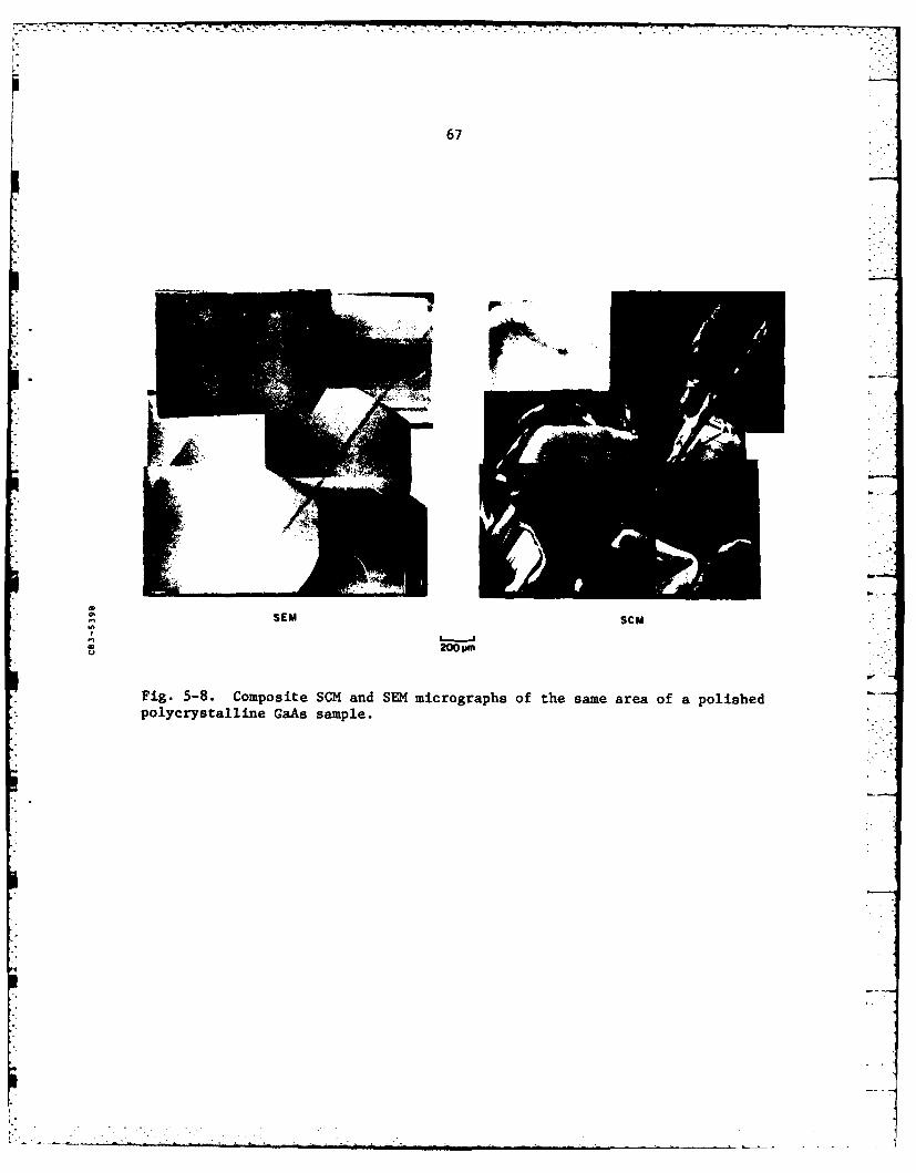
67
*SEM SCM
Fig. 5-8. Composite SCM and SEM micrographs of the same area of a polishedpolycrystalline GaAs sample.

... . U .I .I ...E ui~ .ii .
68
L.
SCM SEM
00M
Fig. 5-9. SCM and SEM micrographs of the same sample area showing fourtypes of grain boundary cathodoluminescene contrast.

69
left of C does not appear in the SEM image. The network structure at the
upper left of the SCM micrograph is probably a dislocation network.
Several additional features have been observed by SCM of
polycrystalline GaAs. First, grain boundaries with similar surface
morphologies can have quite different CL properties. This is illustrated
in figure 5-10 where boundary A shows dark-line CL contrast while boundary
B shows little or no contrast, although their SEM images are similar.
Note also that the contrast associated with boundary B varies along its
length. Second, different regions of a grain boundary with constant
misorientation angle but changing boundary plane have different CL
properties. This is illustrated in figure 5-11 where the CL contrast of
the bright border changes between sections A and B of the same curved
grain boundary. Since the misorientation of these two grains is constant,
this observation indicates that the boundary plane must be considered in
correlating grain boundary structure and properties. Finally, anomalous
bright features appear in many SCM images, such as those labeled C in
figure 5-12. In this figure they are associated with grain boundaries
that exhibit no CL contrast. The results presented in the following
sections suggest that these features are associated with variations in
impurity concentration.
5.3.3 Carrier Concentration and Diffusion Length Measurements
An advantage of CL analysis of polycrystalline GaAs is that it not
only permits qualitative imaging of individual grain boundaries, but it
can also be used to measure carrier concentration and diffusion length on
a microscale. This is extremely useful for analysis of the features
observed by CL imaging. There is no other technique that can provide this
IL

70
SCM SEM
CO 100MU
Fig. 5-10. SCM and SEM micrographs of the same sample area showingdifferent CL contrast from grain boundaries with similar surfacemorphologies.

71
B
SEM SCM
100 pm
Fig. 5-11. SCM and SEM micrographs showing variation in cathodolum-inescence contrast with change in grain boundary plane.

72
4
Acl
44 r.~
0
E-0
co.04 t
0 0)
-40
-4
woL -4 Q
4 4CE '4-4 b
12. 00)
bUt
-H -Hto'~C

73
information with such high spatial resolution and without the use of a
charge separation mechanism. It is noteworthy that the carrier
concentrations of the samples measured by this technique correspond to
impurity atom concentrations of approximately 1 part in 104 . There is no
available technique for the direct measurement of such low impurity
concentrations with the required spatial resolution.
Carrier concentration and minority carrier diffusion length
measurements were made in order to identify the mechanisms associated with
the various types of grain boundary contrast observed by SCM imaging.
Figure 5-12 shows composite SEM and SCM micrographs of the same sample
area. The SEN shows several straight grain boundaries and a long, curved
grain boundary. The SCM contrast displayed by the curved boundary is the
dark line with bright borders type. In this case these borders are so
bright that the dark line is barely visible in this micrograph. The long,
straight boundaries show no CL contrast but there are many bright features
associated with them, as indicated by C in the figure.
Carrier concentration and diffusion length were measured at the
points indicated by A and B in figure 5-12 using the methods described
previously. While both locations are in the same grain, point A is in the
bright border adjacent to the grain boundary while point B is located
about 50 Pm further into the grain. The net acceptor concentration in the
bright border (location A) is 9 x 1018 cm -3 while the corresponding value
in the grain (location B) is 2 x 1019 cm 3. Thus the carrier
concentration well within the grain is about twice that in the region
immediately adjacent to the grain boundary. The curve fits of CL
intensity versus accelerating potential giving the minority carrier
diffusion length at locations A and B are shown in figure 5-13. The

74
1.51
> 0
U)
•~ 1.50- .
I .o L.6,uLm _
0.5 / 0 NEAR BOUNDARY* CRYSTAL
-- CALCULATED
0115 20 25 30 35 40 45 50
kV o
Fig. 5-13. Cathodoluminescence intensity versusaccelerating potential at locations A (nearboundary) and B (crystal) indicated in Fig. 5-12.Each curve is normalized to the intensity at 30 kV.
41

75
diffusion lengths at A and B are measured as 1.2 lim and 0.6 vim,
respectively. These results are summarized in table 5-1. Thus it appears
that in the bright region adjacent to the grain boundary the carrier
concentration is lower and the minority carrier diffusion length is higher
* than at a location further into the grain.
These results suggest that many variations in CL intensity appearing
in the SCM micrographs are associated with variations in carrier
concentration. It appears that regions adjacent to some of the dark
boundaries are depleted of dopant. From these results it is inferred that
the dopant is segregated to these grain boundaries and, hence, there mayL
be a compositional influence on grain boundary behavior.
Similar measurements were made on a grain boundary of the contrast
type that appears bright in the SCM image. The grain boundary chosen for
the measurements shoved the greatest increase in CL above that of the
adjacent grains, but this variation was much smaller than that associated
with the dark grain boundary used f or the previous measurement. In this
case the measured carrier concentration was 4 x 1019 cm73 (peak half-width
of 525 A) regardless of whether the beam spot was directly on the grain
boundary or located on the adjacent grain. This result is believed to be
due to an averaging effect arising because the grain boundary volume is
only a small fraction of the total excitation volume for this case where
the measurement is made with the beam spot positioned on the boundary. In
addition, the measurement is inherently difficult since the relatively
small variation in CL intensity indicates that the carrier concentration
at this boundary is only slightly different than that of the adjacent
g rains.

76
TABLE 5-1
CATHODOLUMIINESCENCE ANALYSIS DATA FOR SPECTRA OBTAINEDAT LOCATIONS A AND B INDICATED IN FIGURE 5-12
Carrier Diffusion
Location Half Width ()concentration (cir3) Length (mg)
A 411 9 x 10¹⁸ 1.2
B 465 2 x 10¹⁹ 0.6

77
5.3.4 Grain Boundary Structure, Composition, and Properties
The results presented in the previous section suggest that many of the
features observed by SCM of polycrystalline GaAs may be attributed to
variations in material composition. The next question to address is the
influence of grain boundary structure on observed properties. As was
previously discussed, and shown in figure 5-11, the change in boundary
plane associated with a curved grain boundary can affect its
optoelectronic properties. However, the basic question of what the .-
difference is between grain boundaries that exhibit essentially no SC"
contrast and those that appear as dark lines has not been addressed. -
Samples prepared as thin sections suitable for TEM were examined using
SCM. Some of these samples were found to contain grain boundaries that
show no SCM contrast. Analysis by TEM indicated that these are twin .
boundaries that show no observable dislocation structure. Figure 5-14
shows a TEM micrograph of a no-contrast boundary positioned such that the
boundary plane is nearly parallel to the incident electron beam. Also
shown are selected area electron diffraction patterns from the two grains
which identify this to be a twin boundary. The grains are rotated with
respect to each other about a <110> axis by an angle of approximately
70.5* and the boundary lies in a { 111) plane. Thus it is concluded that
twin boundaries show no significant contrast in SCM imaging and,
therefore, do not have associated non-radiative recombination centers.
The results of CL analysis of polycrystalline GaAs indicate that both
defect structure and composition effects may influence the optoelectronic
properties of grain boundaries. Based on the experiments discussed, the
following possible explanations for the observed variations in grain
boundary contrast are proposed. Boundaries showing no contrast in SCM

78
0
i " 5
Fig. 5-14. Transmission electron micrograph of a non-contrast grainboundary in GaAs. The crystallographic orientations determined fromdiffraction patterns for each grain identify this as a twi,L boundary.
L

79
imaging are coherent twin boundaries with no associated localized misfit
defects. Bright boundaries are proposed to also be twin boundaries but
having associated dopant segregation effects. The grain boundaries
appearing as dark lines in SCM images have localized misfit defects
associated with. their structures that give rise to non-radiative
recombination of charge carriers. Boundaries that appear as dark lines
with bright borders are proposed to have a similar structure, but dopant
segregation to these grain boundaries has resulted in a reduction in the
carrier concentration in the regions immediately adjacent to these
boundaries. These possible contrast mechanisms are summarized in table
5-2. The observed geometric bright features that appear adjacent to the
no-contrast twin boundaries (for example those designated by C in figure
5-12) may also be caused by segregation effects. Their morphologies are
similar to those characteristic of dendritic growth. Such structures may
be associated with cellular growth arising due to interface instabilities
during growth from the melt. There is no direct measurement technique
available for investigating the influence of impurity segregation on the
optoelectronic properties of polycrystalline GaAs. Thus, while these
conclusions appear reasonable, the supporting experimental evidence is
limited.
5.3.5 Implications of CL Analysis on Photovoltaic Devices
No attempt was made to correlate the type of SCM contrast displayed
by grain boundaries with solar cell performance. However, it is
appropriate to propose a number of possible performance degradation
mechanisms that could be associated with the different types of grain
boundaries observed. It seems likely that boundaries showing no CL
U

80
TABLE 5-2
PROPOSED CONTRAST MECHANISMS FOR THE FOUR TYPES OF CLCONTRAST ASSOCIATED WITH GRAIN BOUNDARIES IN GaAs
Proposed Contrast Mechanism
Boundary SCM Image Boundary Structure Impurity Effects
No contrast Twin No(absence of localized
defects)
Bright Twin Yes
Dark High density of ?localized misfit
defects
Dark with bright High density of Yesborder localized misfit
defects
C:
81
contrast are electrically inactive and will not have a significant effect
on device characteristics. Boundaries that appear dark have associated
non-radiative recombination centers that can be expected to reduce
short circuit current and increase series resistance. Such boundaries
that cross a device junction can cause a reduction in open circuit voltage
and fill factor. In addition, impurities concentrated along grain
boundaries could diffuse into epitaxial layers grown on heavily doped
substrates, affecting device performance by altering bandgap states at the
grain boundary or by changing the doping of the device structure. These
effects are consistent with the low open circuit voltages commonly
observed for polycrystalline GaAs solar cells.
5.4 Summary
This chapter has described luminescence analysis of grain boundary
structures characteristic of polycrystalline GaAs grown from the melt.
The optoelectronic properties of the grain boundaries were examined using
electroluminescence and cathodoluminescence techniques. The performance
of epitaxial p-n junction solar cells was compared with their EL behavior,
and CL analysis was performed on p-type polycrystalline GaAs similar to
that used as the substrates for these devices.
These investigations showed that the grain boundaries in this
material can be categorized into several types and that both boundary
structure and compositio influence the optoelectronic properties of
grain boundaries. In addition, the polycrystalline material was found to
contain significant carrier concentration nonuniformities as well as
defects not revealed by surface morphology. No obvious correlation was
observed between boundary surface morphology and optoelectronic

82
properties. Possible implications of these finding on the performance of
polycrystalline solar cells were presented.
81
contrast are electrically inactive and will not have a significant effect
on device characteristics. Boundaries that appear dark have associated
non-radiative recombination centers that can be expected to reduce
short circuit current and increase series resistance. Such boundaries
that cross a device junction can cause a reduction in open circuit voltage
and fill factor. In addition, impurities concentrated along grain
boundaries could diffuse into epitaxial layers grown on heavily doped
substrates, affecting device performance by altering bandgap states at the
grain boundary or by changing the doping of the device structure. These
effects are consistent with the low open circuit voltages commonly
observed for polycrystalline GaAs solar cells.
5.4 Summary
This chapter has described luminescence analysis of grain boundary
structures characteristic of polycrystalline GaAs grown from the melt.
The optoelectronic properties of the grain boundaries were examined using
electroluminescence and cathodoluminescence techniques. The performance
of epitaxial p-n junction solar cells was compared with their EL behavior,
and CL analysis was performed on p-type polycrystalline GaAs similar to
that used as the substrates for these devices.
These investigations showed that the grain boundaries in this
material can be categorized into several types and that both boundary
structure and compositior influence the optoelectronic properties of
grain boundaries. In addition, the polycrystalline material was found to
contain significant carrier concentration nonuniformities as well as
defects not revealed by surface morphology. No obvious correlation was
observed between boundary surface morphology and optoelectronic
* . .

82
properties. Possible implications of these finding on the perf ormerqce of
polycrystalline solar cells were presented.

AD-Ri44 358 ELECTRON IC PROPERTIES OF GRAIN BOUNDARIES IN GRAS: A 2/jSTUDY OF ORIENTED BI..(U) MASSACHUSETTS INST OF TECHLEXINGTON LINCOLN LAB J P SALERNO ET AL. ig MAY 84
UNCLASSIFIED TR-669 ESD-TR-83-066 F19628-80-C-0002 F/G 20/2 N
I flfll..fl~ mflflfH-mEBBhEBhBhEImhhhmhhhhhhmhlmlhhhEElhhhlhI**EEEEEEEEEE!!.

• , .-
....
MICROCOPY RESOLUTION TEST CHARTNATIONAL BUREAU OF STANDARDS- 1963-A

83
6: Growth and Characterization of Oriented GaAs Bicrystal Layers
6.1 Introduction
The results of the previous chapter indicate that both the structure
and the compostion of semiconductor grain boundaries influence their
electronic properties. It is also apparent that the complex grain
structure of melt-grown GaAs makes it inherently difficult to isolate
individual grain boundaries for detailed studies of their electronic
properties. The influence of intrinsic boundary structure on the
electronic properties can only be investigated by studying grain
boundaries with structures that vary in a systematic fashion and have a
degree of interaction with solute atoms that has a negligible effect on
their properties. In addition, the grain boundaries must have geometries
that are suitable for electronic characterization. This chapter presents
a technique developed to grow bicrystals that contain grain boundaries
which satisfy these requirements. This technique permits all nine
parameters that describe the grain boundary macrostructure to be
experimentally preselected.
The technique is applied to the growth of n-type GaAs bicrystal
layers containing tilt boundaries with a rotational misorientation about
the [110] direction ranging from 0 to 30* and a (111) boundary plane with
respect to one grain. Using the convention defined in Chapter 3, this
structure is denoted as 0[110]/(111). These bicrystal layers constitute a
set of [110] tilt boundaries with structures that are systematically
varied by holding constant all the macroscopic parameters that define the
grain boundary structure except the angle of rotation about a single axis.
In terms of the model for a grain boundary based on two interpenetrating

84
lattices, as described in Chapter 3, this requires rotation of one grain
with respect to the other about only one of three possible axes and the
orientation of the grain boundary along a fixed crystallographic plane
defined in one of the lattices. There are no inherent constraints on the
geometry of the bicrystal layers obtained with this technique or the
dimensions and location of the grain boundary plane in the bicrystal
layer.
This chapter describes the bicrystal growth technique, reports the
electrical properties of the obtained grain boundaries, and discusses some
inherent limitations of the growth process. Included is an investigation
of crystallographic orientation on facet formation, growth rate, and
dopant incorporation for GaAs vapor-phase epitaxy (VPE).
6.2 Preparation Technique
There are two basic steps involved in the preparation of the oriented
GaAs bicrystal layers. The first st-up is the fabrication of a substrate
composed of two single crystal GaAs pieces. These pieces are related by
the desired tilt misorientation. The second step is the growth of the
bicrystal layer on this substrate by VPE. The growth is accomplished by
the AsCl3-GaAs-H2 method(10 6) and makes use of the phenomena of epitaxial
lateral overgrowth(10 7-1 12) to form a continuous layer of GaAs containing
two grains with the same orientations as the pieces composing the
substrate.
The GaAs bicrystals are grown on composite substrates prepared by
bonding two appropriately oriented GaAs crystals that are cut from a
single-crystal boule. As shown schematically in figure 6-1, the crystals
have (110) faces and cross sections for bonding are cut perpendicular to

-" .
85
0
I,,
Fig. 6-1. Geometry of a single crystal cut to form thecomponent crystals of a substrate for epitaxial growthof a bicrystal layer containing a [110] tilt boundary.

86
these faces. For the reference crystal, which we also designate as
crystal 1, the cross section is a (TI) plane; for crystal 2, the cross
section is an off-(TIl) plane that is rotated about the (110] direction by
the desired misorientation angle. The cross sections are then polished
and the crystals are encapsulated with a pyrolytically deposited layer of
phosphosilicate glass approximately 0.3 1m thick. One of the cross
sections is coated with photoresist containing particles of a glass
composed of 61.8 PbO, 31.2 SiO 2 , and 7.0 A120 3 percent by weight. The
cross sections are placed in contact, and the crystals are pressed
together and heated in air to above 810*C, the melting point of the glass.
During this process the photoresist is volatilized, and the crystals are
bonded together by a continuous glass film about 5 Pm thick. After
cooling, the composite formed is cut into wafers approximately 20 mils
thick with (110) surfaces. One such wafer is shown schematically in the
upper diagram of figure 6-2. The (110) upper surface is lapped, polished,
and coated by chemical vapor deposition with an SiO 2 layer 0.2 Um thick.
To complete preparation of the substrate, an SiO 2 stripe 35 um wide that
runs along the length of the bonded interface is defined
photolithographically. As shown in the upper diagram of figure 6-2, this
stripe masks the bonding glass film and extends 15 Pm over each of the
GaAs crystals.
Except for the use of composite substrates, the procedure for
obtaining GaAs bicrystals is essentially the same as that employed
previously for preparing single-crystal GaAs layers over insulating films
by means of lateral overgrowth using the AsC13-GaAs-H 2 method of
vapor-phase epitaxy.(1 0 8 -11 1) The properties of such overgrown layers are
comparable to those of conventional GaAs epilayers grown by this method.

87
SiOZ OVERGROWTH
[111]2
13OUNDARY
~15P~M t-.2pm S10 2GaAs
GaAs
BONDING GLASS
Fig. 6-2. Schematic diagrams of a composite substrate (top) and thecross section of the substrate and bicrystal layer grown by vapor-phase epitaxy (bottom).

88
Deposition of GaAs is carried out under conditions selected so that
nucleation of GaAs growth occurs on the exposed (110) surface of crystals
1 and 2 but not on the SiO 2 masking stripe. When the thickness of the
GaAs epilayers on the crystals exceeds that of the Si0 2 , these layers seed
lateral growth over the stripe. This overgrowth continues simultaneously
with vertical growth until the two layers merge to form a continuous film,
after which growth proceeds normally. The lateral growth seeded by
crystal I is bounded by a slow-growing (TI) facet and is therefore much
slower than that seeded by crystal 2. Since the grain boundary in the
bicrystal is located where the two lateral growths merge, this boundary
occurs close to the edge of the SiO 2 stripe over crystal 1, as shown in
the lower diagram of figure 6-2. As a result of the formation of the
facet, the plane of the boundary is a (111) plane regardless of the
misorientation angle of crystal 2.
The choice of the orientations was determined by investigating the
nature of GaAs epitaxial overgrowth on the S1O 2 coated (110) surface. The --
(111) orientation of the reference crystal was required in order to obtain
a single grain boundary plane perpendicular to the (110) surface. This is
a result of the nature of the overgrowth process, as is explained in the
following section.
6.3 Epitaxial Lateral Overgrowth
Epitaxial lateral overgrowth is a surface reaction limited, faceted
growth process by which an overgrowth mask that covers a portion of the
seed surface can be covered by a crystalline layer having the identical
structure and orientation as that of the substrate. The overgrowth mask
is inert in the epitaxial system to the extent that no nucleation occurs

89
on its surface. The growth parameters are adjusted to achieve the
near-equilibrilum surface reaction limited condition for which the
differences in growth rate of the crystallographic planes are maximized.
This results in the formation of macroscopic facets and large differences
in the growth rate of low index planes. The growth rate of high index
planes, however, is relatively high because of the formation of atomic
steps and ledges associated with microfacets at these growth fronts.(1 1 2)
The quality of the overgrown epitaxial layers is comparable to
conventional epitaxial films except for significant lateral variations in
carrier concentration.(111) These carrier concentration nonuniformities
are the result of differences in dopant incorporation by the facets that
form during the overgrowth process.
6.3.1 Orientation Dependence and Facet Formation
The orientation of the overgrowth mask on the substrate surface
determines the nature of the faceting along the lateral growth front. A -
special overgrowth mask was used to study this selective nature of the
lateral overgrowth process. The pattern of this mask is a circular array
of pairs of radial slit openings that are indexed at 16 intervals over the
full 360. This spoke pattern allows the observation of the formation of
the continuous epitaxial layer by the merger of lateral overgrowth fronts
that eminate from the parallel seed openings. In addition, the nature of
the lateral overgrowth facets can be studied as a function of the
orientation of the slit openings on the single crystal substrate.
Figure 6-3 shows the result of lateral overgrowth from such a spoke
pattern with 2 um wide slit openings on a (110) GaAs substrate. The
growth conditions are the same as those used for the bicrystal layer

90
[110] [)TO]
[001 1
(001]
Fig. 6-3. Selective GaAs epitaxial overgrowth from a spoke pattern of radialstripe openings at l* intervals on an Si0 2 coated (110) surface. Brightregions are GaAs and dark regions are S102. The 30* orientation range usedfor bicrystal growth is indicated.

91
growth, to be discussed later. The polished (110) GaAs substrate was
coated with 1000 A of chemical vapor deposited SiO 2 and the spoke pattern
was formed in the SiO 2 by photolithography and chemical etching to expose
the GaAs surface at the slit openings. In this figure the bright areas
are epitaxial GaAs and the dark areas, including the center, are exposed
SiO 2. It is apparent that nucleation and growth did not occur on the
central SiO 2 disk. There are twelve orientations for which essentially no
overgrowth occured, leaving the SiO 2 regions of the spoke pattern still
exposed. These orientations are indexed as to which planes would be
exposed if the lateral growth facets were perpendicular to the substrate.
In general, however, these are not the indices of the facet planes that
form the lateral growth fronts.
The range of misorientation angles employed for the bicrystal layer
growth is indicated in figure 6-3. The (Tl1) facet forms vertical to the
(110) and, being the As or "B" face, essentially forms a stationary, or
"bounding" facet. This is one of the overgrowth fronts that meet to form
the grain boundary. This orientation is used as the reference crystal of
figure 6-2 and defines the macroscopic grain boundary plane. The lateral
growth front that meets this (TI) facet to form the grain boundary in the
bicrystal layer will have the same facet structure as the front facing the
(111) facet in figure 6-3 but eminating from the seed slit that is rotated
from the (T11) facet by an angle equal to the misorientation angle of the
grain boundary.
The facet structures of these growth fronts were examined by scanning
electron microscopy (SEM) of the overgrowth spoke pattern. Micrographs of
the (T11) facet and the growth fronts at 2, 10, 15, 24, and 30* off the
(111) plane are shown in figures 6-4 through 6-9. Note that the lengths

92
SSiGaAs
2.5 /m
Fig. 6-4. SEM micrograph of a laterial overgrowth frontseeded in a stripe opening parallel to (111).
GaAs
Fig. 6-5. SEM micrograph of a laterial overgrowth frontseeded in a stripe opening oriented at 20 off (111).

93
GaAs
Fig. 6-7. SEM micrograph of a laterial overgrowth frontseeded in a stripe opening oriented at 150 off (111).
GaAs
-- .
Fig. 6-6. SEM micrograph of a laterial overgrowth frontseeded in a stripe opening oriented at 108 off (111).

94
GaAs
Sio
- 0
Fig. 6-8. SEM micrograph of a laterial overgrowth frontseeded in a stripe opening oriented at 240 off (111).
GaAs
I I
Fig. 6-9. SEM micrograph of a laterial overgrowth frontseeded in a stripe opening oriented at 30° off (111).

95
of the fronts are much greater than indicated by the micron marker because
of the near-90* tilt of the specimen required to obtain the SEM
micrographs. Figure 6-4 shows that the (TI) overgrowth front consists of
a single facet perpendicular to the (110) surface. The front at 2* off
(Ti), that would Join the (TI) facet to form a 2*[1101/(T1) grain
boundary if grown on a composite substrate, is shown in figure 6-5 to be
nearly a single facet. This is in contrast to the multifaceted front,
shown in figure 6-6, that forms when the slit opening is oriented at 100
off (111). For an orientation of 15* off (111) the overgrowth facet is
beveled along its length and has a fine facet structure perpendicular to
the bevel. The faceting along the lateral overgrowth fronts at 24 and 30*
off (M11), shown in figures 6-8 and 6-9, respectively, is extremely coarse
and appears somewhat random. The key point, however, is that the faceting
along a lateral overgrowth front varies significantly with orientation.
Also note that the (110) epilayer surface contains arrays of facets.
This faceting takes place because the substrate orientation deviates slightly
from (110). Such faceting is also found on the surfaces of bicrystal layers
grown on composite substrates with slight, unintentional deviation from the
(110) surface orientation.
6.3.2 Orientation Dependence of Growth Rate and Carrier Concentration
The occurance of facets along the lateral overgrowth fronts has been
established. In addition, it was found that the nature of faceting is
dependent on the orientation of the overgrowth mask on the substrate surface.
Previous investigations(1 11) have revealed that the different facets
incorporate dopant atoms at differing rates with the result of nonuniform
carrier concentration in the overgrown epitaxial layers. The quantitative

96
determination of the carrier concentration in overgrown regions is difficult
because of the small geometries involved. In order to investigate the dopant
incorporation behavior of the relevant growth fronts, single crystal
substrates were prepared with surface orientations of interest for the
bicrystal growth.
Single crystal substrates with (110) and (TI1) orientations and 10, 24,
and 30* off (11) were prepared from a single-crystal high-resistivity p-type
boule. Two epitaxial growth runs were made with substrates of all five
orientations present in the reactor for each of the runs. Growth was done by
the AsCl 3-GaAs-H 2 method in a reactor described elsewhere.(10 6) The growth
conditions were identical to those used for the bicrystal layers. The
substrate temperature during growth was 720*C and the GaAs source temperature
was 830*C. One growth run was unintentionally doped n-type (presumably by Si)
while the second run was doped n-type with S using H2S. The growth rate was
determined from the optically measured thickness of the epitaxial layer after
staining with 10 K3Fe(CN)6 10 KOH 100 H20 by weight. The carrier
concentration was measured using conventional capacitance-voltage
techniques(1 13) with a Hg Schottky contact probe.
The growth rates and carrier concentrations of the ten epitaxial layers
grown for this study are plotted as a function of substrate orientation in
figure 6-10. It can be seen that the influence of substrate orientation is
very pronounced. The growth rate is found to be nearly independent of the
dopant type but is seen to vary by up to a factor of 40 with substrate
orientation. The data are qualitatively consistent with the relative growth
rates of the lateral overgrowth fronts shown in figure 6-3. The slowest
growing orientation is (111). However, the influence of substrate orientation
on carrier concentration is found to be dependent on the dopant specie. This

- + . .. - . .......
97
fill) fill) tli ) fill) (110)
o UNDOPED CARRIER CONCENTRATION0 UNDOPED GROWTH RATE _102
aa SULFUR DOPED CARRIER CONCENTRATIONSULFUR DOPED GROWTH RATE
E
U 02E
0 O 11
,31:
i -EFi. 6-v m a
..... s o

98
effect is most apparent when comparing the carrier concentration on (T11)
to that on a substrate 10* off (111). For the undoped run the carrier
concentration is lower for growth on (TI) than for growth 100 off (1I1), -
whereas this relationship is reversed for the S-doped run. There is no
apparent relationship between carrier concentration and the growth rate.
These results suggest that the chemical potential of a particular dopant
specie is dependent on the surface orientation and, in addition, that the
nature of this dependence is unique to the particular impurity element.
The epitaxial structures for which these data were obtained are
obviously different from those obtained by lateral overgrowth. However,
the general trends of the dependence of carrier concentration on
orientation are expected to apply. The implication of these results on --
the bicrystals prepared by this technique is that it is possible to have a
large difference in carrier concentration from one side of the grain
boundary to the other. For instance, a 24* [1101/(111) boundary formed by
laterally growing fronts in an undoped layer could have a carrier
concentration on the (11) reference crystal side twenty times that of the
other grain. It will be shown that, although such a carrier concentration
gradient does not dominate the grain boundary properties, its effect is
apparent. The carrier concentration nonuniformities in the vicinity of
the grain boundary are, in general, considerably more complex than
presented here because of the many facets that occur along a single
lateral overgrowth front. Although these nonuniformities are only of a
secondary effect on the grain boundary properties, they will be shown to
considerably complicate the analysis of the electronic structure
associated with the grain boundaries.

99
6.4 Growth of Bicrystal Layers
The effects of intrinsic boundary structure and donor concentration
on the electronic properties of grain boundaries in GaAs were studied on
twelve bicrystal layers. These were grown in four separate deposition
runs, as sumarized in table 6-1. All VPE was done using the same process
and growth conditions as described in the previous section for growth on
the crystal substrates. The substrate temperature during growth was 720*C
and the temperature of the GaAs source was 830*C. All layers were about
30 Pm thick. For one deposition run, nominally undoped bicrystal layers
were prepared with the previously described geometric structure and
misorientation angles of 10, 24, and 30% The layers grown in a second
run were also nominally undoped but the grain boundary misorientation
angles were 2.5, 5, and 10. These substrates were prepared at 2* off the --
(110). The third and fourth depositions produced S-doped bicrystal layers
containing 100 tilt boundaries. A control sample, designated as a "0*
bicrystal," was included in all growth runs to serve as a baseline for
electrical characterization. This layer was also grown on a composite
substrate which is formed, however, from two crystals having bonding
cross sections cut 10° from the (TIl) plane. Thus the grain boundaries
formed in these epitaxial layers have different structural geometry than
those grown on the other substrates. It would have been desirable to
prepare the 0* bicrystals with a (Til) boundary plane, as was done with
the other orientations. However, this would require the use of a
substrate formed from two crystals with (T11) and (111) cross sections,
necessitating an unrealistic growth time because of the slow lateral
growth rate in these directions. The substrate dimensions parallel and
perpendicular to the long direction of the SiO 2 masking stripe were 1.2

100
TABLE 6-1
SUMMARY OF BICRYSTAL GROWTH RUNS
Hisorientation Substrate Surface
Run n(110 ) (cw-3) Dopant Angles Orientation
-9
1 1.0 x 10¹⁵ Undoped 00, 10* 24*, 30- (110)
2 2.5 x 10¹⁵ Undoped 0o , 2.50, 5', 10- 2° off (110)I
3 9.0 x 10¹⁵ S 00, 10. (110)
4 1.0 x 10¹⁸ S 00, 100 (110)
i
1.
101
and 0.5 cm, respectively. The crystals used to form the composite
substrates were all cut from nominally undoped high-resistivity p-type
single-crystal GaAs boules. A conventional epitaxial layer was also grown
in all deposition runs on a single-crystal (110) substrate. The quoted
carrier concentrations were measured on this epilayer.
The effect of intrinsic structure on grain boundary properties could
be evaluated by studying the undoped layers over a range of misorientation
angles from 0* to 30. The effect of donor density on grain boundary
properties could be evaluated by studying the four grain boundaries with
the same 10°[110]/(111) geometric structure but with carrier
concentrations ranging from 1 x 10¹⁵ to 1 x 1018 cm- 3 . All the bicrystal
layers, except the 0* controls, are formed with one grain having the (TiI)
reference orientation. Thus the lateral overgrowth fronts seeded on these
crystals should grow with the same carrier concentration for a given
deposition run. This permits the comparison of the properties of grain
boundaries in bicrystal layers grown in the same deposition run even
though the carrier concentration in the epilayers seeded on the
misoriented crystal varies between samples with different misorientation
angles.
Figure 6-11 shows Nomarski interference contrast micrographs of
as-grown surfaces of the 00 and 240 bicrystal layers grown in deposition
run one. The observed structure is typical of all layers grown on
substrates having no intentional misorientation from the (110) surface,
e.g. deposition runs one, three, and four. In each case the trace of the
grain boundary is quite straight, indicating that the rate of lateral
growth for each component crystal was uniform along the length of the S10 2
stripe. Notice that the two overgrowth fronts that form the 00 grain
I

K 102
00
240
(1T2j 2 i 1
Fig. 6-11. Nomarski contrast micrographs of 0 and 240 GaAs bicrystallayers grown on substrates with (110) surface orientations.

103
boundary join together so well that the boundary trace is not well
resolved. As was observed in the SEM micrographs of figures 6-4 through
6-9, facets form on the surface due to its unintentional slight
misorientation from (110). These facets appear in the Nomarski contrast
as parallel straight lines on each grain that continue across the grain
boundary at an angle that corresponds to the misorientation angle e.
It is general practice in VPE to improve surface morphology by the
use of substrates intentionally misoriented from a low index plane. This
technique was employed by misorienting the composite substrates for
deposition run two by 2* from the (110). The effect on surface morphology
is evident from the Nomarski contrast micrograph of the as-grown surface
of the 100 bicrystal layer shown in figure 6-12. Note that different
surface morphologies are observed for the areas of conventional epitaxy
and the region of rapid lateral overgrowth seeded on the off (111) grain.
It is apparent that little overgrowth occurs from the (Til) reference
crystal, as is expected. All bicrystal layers grown on substrates
intentionally misoriented from the (110) showed this improved morphology.
Figure 6-13 shows Laue back-reflection x-ray diffraction patterns
taken for the four bicrystal layers of deposition run one. In each case
the x-ray beam, which was about 1 mm in diameter, was approximately
centered on the grain boundary and aligned parallel to the [110] axis of
the reference crystal. (For the 0° bicrystal the designation of a
reference crystal is arbitrary since neither crystal has a (T11) cross
section.) Therefore each photograph shows two (110) patterns rotated with
respect to each other by the angle 0 about the [110] tilt axis. In each
case the [110] poles are slightly displaced from each other, indicating a
deviation from the pure tilt orientation. The deviations, which have been

104
B
100/m -,
100
Fig. 6-12. Nomarski contrast micrographs of 100 GaAs bicrystal layer grownon a substrate surface oriented 2* off (110).
0_ _
-9

105
Fi. -1. ac-rflctonLuex-aydifrctonpaten i o foriented Ga~s bicrs aes

106
measured from both the Laue patterns and x-ray diffractometer scans,
correspond to rotations of less than V about the [Till and [IT2]
directions, the axes orthogonal to [1101. Similar results were obtained
for bicrystal layers with the 2.5* and 5" misorientation angles. Thus the
unintentional misorientation of the non-0" bicrystals is small compared to
0. The values of 0 measured from the Laue patterns are 10.1, 24.0, and
30.5, with an estimated uncertainty of 0.5, compared with intended
values of 10, 25, and 30. Values of 0 of 2.5* and 5* for the two other
grain boundary structures were verified to within the uncertainty of the
measurement technique.
6.5 Electrical Characteristics
In order to measure the electrical characteristics of grain
boundaries in the oriented bicrystal layers, specimens 1.5 mm wide and 5
mm long were prepared by making a series of saw cuts perpendicular to the
grain boundary and extending through the bicrystal layer and substrate.
An hour glass shaped mesa about 0.5 mm wide at the grain boundary was
defined in the epitaxial layer of each specimen, as shown schematically in
figure 6-14, by masking the as-grown surface and etching down to the
substrate with 5 H2SO4: 1 H202: 1 H20. Any epitaxial growth on the back
of the substrate was also removed. Four ohmic contacts, two on each
grain, were made by alloying 250 um diameter Sn spheres to the mesa at
300*C for 2 minutes in an HC1-H2 ambient. With this test structure,
electrical conduction between contacts on opposite sides of the grain
boundary is restricted to the bicrystal epilayer since the two crystals
in the substrate are isolated by the bonding glass layer. In all cases,
current voltage (I-V) measurements between the two contacts on the same

107
Sn
CONTACT
0 "
~SUBSTRATE
Fig. 6-14. Mesa structure for electrical characterization of agrain boundry in a bicrystal epitaxial layer.

108
grain gave linear characteristics, showing that the contacts were ohmic.
The grain boundary area was determined, to an accuracy of about 20%, by
optical microscopy. For all samples the grain boundary area was on the
order of 10- 4 cm2 .
Figures 6-15 and 6-16 show, respectively, the room temperature I-V
characteristics obtained by measurements across the grain boundaries
prepared in deposition runs one and two. To facilitate comparison, the
curves are plotted (except for the 0* specimens) so that the portion in
the first quadrant shows the behavior obtained when a positive reverse
bias is applied to the (Til) reference crystal. The characteristic for
the 30* grain boundary is not shown in figure 6-15 but is similar to that
for the 24° specimen.
It is observed that both 0* specimens show linear I-V
characteristics, indicating that no potential barrier is present. As the
misorientation angle G is increased to 10° , the characteristics become
increasingly non-linear indicating a potential barrier is developing.
Strong rectification is exhibited by the 10° boundary with n(ll0) - 2.5 x
1015 cm 3 , consistent with the back-to-back diode characteristic
associated with the formation of a double-depletion region due to
Fermi level pinning by grain boundary states. The band structure
suggested by these characteristics is schematically shown in figure 6-17.
Note the asymmetry of the I-V characteristics of the 10° and 240 grain
boundaries dictated by a lower carrier concentration in the off (T11)
grain of the bicrystal layer. The rectification is seen to be larger for
the I0° boundary in the n(l0) - 1 x 1015 cm- 3 layer than for the
equivalent structure in the n(110) - 2.5 x 1015 cm- 3 layer and largest for
the 24* grain boundary. The rectification associated with a 30° boundary

109
[lio]
Fig. 6-15. I-V characteristics measuredacross (1101 tilt boundaries with
n(110) 1.0 x 1015 cm-3
*(110

110
2.50 [no]
50°[io]
100[io]
Fig. 6-16. I-V characteristics measuredacross [110] tilt boundaries withnl( 1 1 0 ) ; 2.5 x 101 5 cm- 3 .

111
Ec
~BOUNDARYSTATES
d
EQUILIBRIUM
i ( .. ..... e + eVEc.
EF
E V
BIASED
z EQUIVALENT CIRCUIT
Fig. 6-17. Grain boundary band structure model for ann-type semiconductor showing the double-depletionregion for the zero-bias equilibrium and biased config-urations and the equivalent circuit.

112
is similar. These results indicate that the grain boundary transport
properties are determined by both the boundary structure and the donor
density in the grains. The observed increase of the reverse bias
breakdown voltage with increasing e corresponds to an increase in the
density of grain boundary bandgap states. The lowering of the height of
the grain boundary potential barrier, *B, with increasing donor density is
consistent with the Fermi-level pinning/double-depletion-region
model.(24)
Referring to the discussion in Chapter 5, CL images of the
10-[1101/(T11) structure with n(1 1 0) - I x 1018 cm-3 shows this boundary
to exhibit dark line contrast. The features associated with carrier
concentration variations and impurity segregation in the melt-grown GaAs
were not observed in the VPE bicrystal layer. The CL analysis could not
be performed on bicrystal layers from other deposition runs because of
their lower carrier concentrations.
6.6 Summary
A technique has been presented for the growth of oriented GaAs
bicrystal layers containing [110] tilt boundaries with a preselected
misorientation angle and a (Til) boundary plane. It should be possible to
apply the technique to other grain boundary structures and other materials
that exhibit epitaxial lateral overgrowth. The technique has been used to
prepare n-type GaAs bicrystal layers with 0 up to 30" which were suitable
for investigating the electronic properties of grain boundaries in GaAs as
a function of boundary structure and donor concentration in the grains.
The structures of the grown bicrystal layers were demonstrated to be

113
consistent with those expected from the study of the epitaxial lateral
overgrowth process.
Grain boundary specimens suitable for electrical characterization
were fabricated. The I-V characteristics measured across the grain
boundaries are found to be consistent with a double-depletion-region model
for the grain boundary band structure. The characteristics of 0i
bicrystal control specimens indicate potential barrier formation is not
inherent to the overgrowth process. The height of the grain boundary
potential barrier is determined by both the donor concentration in the
grains and the density of grain boundary states. The density of the grain
boundary states appears to increase with e until saturation occurs in the
240 to 30* range. The I-V characteristics of the strongly rectifying
grain boundaries were found to be asymmetric. This effect is consistent
with the orientation dependence of dopant incorporation associated with
the epitaxial lateral overgrowth process. The following chapter will
present a quantitative investigation of the influence of the intrinsic 4
boundary structure and donor density on the electronic structure of grain
boundaries in GaAs.
1 . . -. 1 .. . . -. . .•

. . ... ..... ... ..
115
7: Electronic Characterization of Oriented Bicrystal Layers
7.1 Introduction
The results of the preceding chapter indicate a relationship between
the geometric structure and the electronic properties of grain boundaries
in GaAs. The observed properties arise due to the electronic band
structure associated with the grain boundaries. This band structure is
characterized by a potential barrier to majority carrier transport
resulting from the trapping of majority carriers at bandgap states. This
chapter discusses how the potential barrier height and the density of the
bandgap states varies with the misorientation angle characterizing the
structure of the grain boundaries in the epitaxial bicrystal layers.
The electronic properties of the prepared grain boundaries were
determined from their current density-voltage (J-V) and
capacitance-voltage (C-V) characteristics. These data provide information
on the variation of potential barrier height and the equilibrium density
of carriers trapped by grain boundary states as a function of the
misorientation angle. In addition, deep level transient spectroscopy
(DLTS) was employed to obtain the positions and relative densities of the
boundary states in the bandgap. First, the experimental techniques will
be discussed followed by the results and their implications for the
physical structure of the grain boundaries.
7.2 Experimental
The current-voltage characteristics displayed by the prepared grain
boundaries have been shown to be consistent with the
double-depletion-region model for the electronic band structure. The

116
asymmetry of the observed characteristics, however, indicates that the
carrier concentration differs from one grain to the other. In addition, a
previous investigation(I11) of the lateral overgrowth process suggests
that complex carrier concentration nonuniformities can exist in the
regions adjacent to the grain boundaries. The electronic band structure
of such a grain boundary in an n-type semiconductor is schematically given
in figure 7-1. In this figure, the donor densities in grains 1 and 2 are
characterized by the effective values N1 and N2 , respectively; the
respective zero-bias barrier heights are *1 and f2 and the positions of
the Fermi level below the conduction band in the grains are given by 61
and 62. The upper diagram of figure 7-1 shows the zero-bias band
structure for N1 > N2 and, hence, fI > f2 and 6 1 < 8 2 . The respective
depletion regions in each grain have widths of dl and d 2 - The lower
diagram of figure 7-1 shows the band structure when a bias voltage, Va, is
applied across the grain boundary such that grain 1 is reverse biased.
The J-V, C-V, and DLTS analysis techniques will be discussed in terms of
this model.
7.2.1 Current-Voltage Analysis
When a reverse-bias voltage is applied across a grain boundary, as
shown in figure 7-1, electrons flow from grain 2 to grain I in response to
the decrease in the Fermi level in grain 1 by an amount eVa. It can be
assumed that the drop in applied voltage occurs entirely across the
reverse-biased side and that the flow of current occurs due to thermionic
emission over the barrier.(2 4 ,4 1,6 5) (For GaAs it appears that electron
tunneling through the grain barrier contributes to current flow only for
carrier concentrations exceeding 1017 cm- 3.(6 1)) Under these conditions

117
GRAIN 2 GRAIN I
ET
E
N1
zE
oV
e.j
00
Fig. 7-1. Band structure model for a grain boundary inan n-type semiconductor with different carrier concen-trations in each grain such that NI > N2 at zero-bias(top) and for a reverse bias voltage Va applied to giain L .1 (bottom).

118
the barrier height of the forward-biased grain remains constant at the
zero-bias equilibrium value while that of the reverse-bias side changes in
response to Va.(2 4,4 1) The current flowing from grain 2 to grain I is
given by
J21 = A*exp[-(62 + *2)/kT , (VII-)
while the current flowing from grain 1 to grain 2 is given by
J12 - A*exp[-(61 + I + eVa)/kT, (VII-2)
where A* is a modified Richardson constant taking into account the
probability of electron capture by the grain boundary states. The net
current flow across the grain boundary is the difference of equations
(VII-1) and (VII-2) and is given by
(VII-3)J = A*exp1-(62 + 2 )/kT] - A*exp[-(61 + 01 + eVa)/kT]
Rearranging terms(VII-4)
J = A*{exp[-(62 + #2)/kT - exp[-( 6 1 +* 1 )/kT] exp[-eVa/kT]l
The equilibrium Fermi level of the grain boundary itself is
6 GB z + 6 1 2 + 62 • (VII-5)
Thus equation (VII-4) can be rewritten as
J - A*exp(-6GB/kT)[I - exp(-eVa/kT) ] (VII-6)
It is seen from equation (VII-6) that the current flowing at a given
applied voltage is determined by the value of 6G0- In turn, the value of
6GB is primarily determined by the potential barrier height since 61 and
119
62 are small compared to $I and f2 for highly rectifying grain
boundaries.
The electronic charge density trapped by the grain boundary states at
zero bias is equal in magnitude to the positive space charge density in
the depletion regions and is given by(11 4)
Qo[coul/cm2 ] - (2CoCrNjj)1/ 2 + (2orN242) 1 / 2 . (VII-7)
The excess trapped charge density occuring due to a reverse-bias voltage
Va applied to grain 1 is(2 4)
QE (2 oereN Va) 1 / 2 (VII-8)
At a sufficiently high applied reverse-bias voltage (breakdown or
saturation voltage) the available excess grain boundary states become
filled and the potential barrier collapses. The collapse of the barrier
is accompanied by a rapid increase in current with applied voltage. From
equation (VII-8), the breakdown voltage is given by
2Vmax = 2 dfreNiQmax , (VII-9)
where Qmax is the maximum charge density that can be contained in the
grain boundary.
Note that Vmax is determined by both the density of grain boundary
states and the carrier concentration of the reverse biased side. Thus in
comparing the J-V characteristics for transport across the grain
boundaries in the bicrystal layers it is only appropriate to consider the
characteristics for reverse bias of the common (T11) reference crystal.
This is because only this orientation form the same overgrowth front and,

120
therefore, has the same carrier concentration for every bicrystal layer
grown in the same deposition run.
The J-V characteristics for reverse bias of the (1Il) side of the
bicrystal layers described in table 6-1 were obtained from two-point
measurements of current for an applied voltage. The voltage source was a
Systron-Donner MI06A d.c. voltage source and the current was measured
using a Keithley 445 digital picoammeter. All measurements were made in
the dark at room temperature. The specimens were prepared as described in
Chapter 6. The ohmic contacts on the samples were connected to 7 mil
diameter Au-wire probes.
7.2.2 Capacitance-Voltage Analysis
As discussed in Chapter 6, the grain boundary can be treated as two
back-to-back diodes. Thus the grain boundary capacitance is given by the
series sum of the capacitances of the two Schottky diodes represented by
the space charge region in each grain.(24 ,6 3 ) The grain boundary
capacitance, C, is given by
1 = I + 1 (VIlI-lO)
C Cl C2
where C1 and C2 are the capacitances due to the space charge regions in
grains 1 and 2, respectively. For the bias conditions shown in figure
7-1, where a reverse-bias voltage Va is applied to grain 1, C1 and C2 are
given by(1 14 )
C -[ e2 acorl 1/2 (VII-If)A [2#_1 TeVakT M

121
and
___2 [1/2C2 . e o]rN2 (VII-12)A 2(*2 - kT)
where A is the grain boundary area and it is assumed the applied voltage
drop occurs entirely across grain 1. Assuming kT/e is negligible, the
total grain boundary capacitance is given by
(VII-13)
C e2A2C oer Ni N2
This is the capacitance equation for the general grain boundary structure L
shown in Fig. 7-1. The corresponding depletion widths are (114)
1/2 1/2
d1 -( 2 °cr )e (*1 + eVa )1 (VII-14)
and
d coer 1/2 1/2 (VII-15)
The total charge in the grain boundary states is
Q - eA(Njdj + N2d2) . (Vii-16)
For the case of zero-bias equilibrium, Va - 0 and equation (VII-13)
becomes
112 ) 1/2 1/211 (_2 + (r t VI-7
1 '(e2A2eo ) r i 2
where CO is the capacitance at zero bias. It also follows that
2 Cocr )1/2 1/2 (VII-18)
(- (

122
d i/2 2 , (VI-19)
and
Q. " A(2coer)1/ 2 [(Nl 1)'/2 + (N2 2 ) 1 / 2 ] " (VII-20)
For the special case of NI = N2 and, therefore, *j = 2
1 , 2 2 1/2 2 1/2 (VII-21)e2A2 O r (2
Comparing this to equation (VII-12) it is seen that, even when a reverse
bias is applied to grain 1,
C2 2C0 (VII-22)
if N, - N2. When these restricted conditions apply it is easy to
determine the values of NI - N2 and *1 *z using conventional C-V
analysis since
1 1.. 1 ,(VII-23)C1 C 2C0
where CO is the measured zero-bias capacitance and C is the measured
capacitance at a bias voltage Va.(6 3) Unfortunately, this type of
analysis is not applicable to the bicrystal specimens prepared by lateral
overgrowth since N, * N2. However, Appendix 3 presents a procedure for
the self-consistent analysis of the C-V characteristics for the general
grain boundary structure of figure 7-1. Using this procedure, effective
values of NI, N2 , 1, 2, 61, 82 can be obtained and used to calculate the
actual charge in the grain boundary states at zero-bias equilibrium.
Two measurement systems were used for the C-V measurements. One made
use of a Systron-Donner MI06A d.c. voltage source and a Boonton
Electronics 76A I MHz capacitance bridge; the second made use of a

123
Princeton Applied Research 410 C-V plotter. All measurements were made by
applying a d.c. bias voltage with a superimposed 20 mV a.c. signal at a A
frequency of 1 MHz. The charge trapped at GaAs grain boundaries does not
follow the 1 MHz signal.(63 ) All measurements were made in the dark at
room temperature. The C-V data was analyzed using the procedure described
in Appendix 3. Only low donor density specimens with e > 100 could be
analyzed by C-V analysis since this measurement requires a low
conductance.
7.2.3 Capacitance Transient Analysis -
The nature of the grain boundary states was investigated by using a
modification of the DLTS technique presented in Appendix 1. For this
analysis a pulsed d.c. bias was applied across the grain boundary to fill
additional bandgap states. Upon termination of a I volt bias pulse of
0.4 msec duration the capacitance associated with the grain boundary space
charge region was monitored at 1 MHz using a Boonton Electronics 72B
capacitance meter. The capacitance transient accompanying the return to
the zero-bias equilibrium band configuration was analyzed using either a
Princeton Applied Research 162 dual gated boxcar averager or a PrincetonL
Applied Research HR-8 lock-in amplifier. The lock-in amplifier resulted
in a signal with a better signal-to-noise ratio while the boxcar averager
was useful for obtaining preliminary DLTS spectra that provided the-
general peak locations.
The capacitance transient was analyzed as a function of temperature
as described in Appendix 1. Unlike in conventional DLTS analysis, theI _
traps in the grain boundary space charge region cannot be emptied to a
level below the zero-bias Fermi level position, 6GB. This is because any
L_ _

124
applied voltage configuration results in one grain being reverse biased
and the other being forward biased and, thus, the filling of additional
grain boundary states. Thus only grain boundary bandgap states with
energies above the zero-bias Fermi level can be analyzed using this
capacitance transient technique. This analysis enables the determination
of the energies and relative densities of bandgap states in the space
charge regions using the procedure described in Appendix 1.
Since the DLTS analysis detects electronic states in the entire space
charge region, not only those at the grain boundary plane, both grain
boundary states and bulk states in the grains appear in the spectra. In
order to distinguish the bulk traps from the grain boundary states, a
Au-Schottky contact was placed on a 0° fabricated grain boundary and
analyzed using conventional DLTS. This technique is not applicable for
the analysis of the grain boundary states themselves because the space
charge region of such a contact geometry includes only a negligible
density of grain boundary states.
The voltage pulse filling of grain boundary states is only useful for
the quantitative analysis of electron traps. Optical excitation was
employed to investigate the presence of hole traps. This analysis showed
the same bandgap states observed using voltage pulse filling. Thus only
electron traps were detected in the bandgap at energies above the
zero-bias Fermi level. For this reason only the results of voltage pulse
DLTS will be discussed further.
7.3 Results and Discussion
Figure 7-2 shows the room temperature J-V characteristics for current
transport across grain boundaries in unintentionally doped bicrystal

125
101
100-E
101-
1 1. 2
1OzwL
C2
2.6 102-115Cr'
1010 24 71 a90 1.0lt1fV
VOLTAGE IV)
Fig. 7-2. 3-V characteristics for reverse bias of the (i11)grain as a function of tilt angle.
L.

126
layers with 0 ranging from 0* through 30. These characteristics were
obtained with a reverse bias voltage applied to the common (111) oriented
grain, except for the 00 specimens. The samples were prepared in two
deposition runs. Grain boundaries with tilt angles of 0, 2.5, 5, and 100
were grown in desposition run 2 yielding n(110) - 2.5 x 1015 cm- 3 while
grain boundaries with tilt angles of 10, 24, and 30* were grown in
desposition run 1 with n(1 10) - 1.0 x 1015 cm-3. The J-V charactersitics
were measured for either 2 or 3 specimens cut from each bicrystal layer.
The plotted curves are those for the specimens exhibiting the smallest
low-bias current density, interpreted as having the lowest leakage p -
currents, but are typical of the observed characteristics. These
characteristics allow the analysis of the influence of the grain boundary
geometric structure on the grain boundary electronic properties. S .
The rectification associated with the tilt boundaries increases with
the misorientation angle for all these samples. From the analysis
presented in section 7.2.1, however, the characteristics of the 10, 24, j
and 30* grain boundaries indicate that the potential barrier height is
constant and, thus, independent of misorientation angle. The slight
rectification displayed by the 2.5 and 5* grain boundaries indicates that
the donor density of these layers is sufficiently high to essentially fill
the grain boundary trap states.
The reverse-bias voltage at which J begins to increase rapidly with
applied voltage (the breakdown or saturation voltage) is observed to be a
strong function of 0. These data indicate that the density of grain
boundary states increases with misorientation angle until saturation
occurs for 0 in the range of 24 to 30, suggesting that the density of
grain boundary states is directly related to the grain boundary structure.
!I
127
The J-V characteristics indicate that the electronic band structure
associated with a grain boundary is influenced by the intrinsic structure
of the grain boundary. Moreover, assuming the density of grain boundary
states is determined by the bonding configuration at the interface, the
atomic arrangement associated with the grain boundary is found to be
related to the geometric structure of the grain boundary.
The J-V characteristics of the 10* tilt boundaries with donor
densities of 1.0 and 2.5 x 1015 cm- 3 indicate that * decreases as the
carrier concentration in the grains increases. This effect is consistent
with the double-depletion-region model based on Fermi level pinning by
grain boundary states. To investigate this further, the J-V
characteristics of four 10* [110]/(T11) tilt boundaries in bicrystal
layers grown in separate desposition runs with n(1 1 0) ranging from 1.0 x
1015 to 1.0 x 1018 cm- 3 were determined with the reverse-bias voltage
applied to the common (TI) oriented grain. These characteristics are
shown in figure 7-3. The data show a decrease in grain boundary
rectification with increasing carrier concentration. This is attributed
to both a decrease in grain boundary barrier height, due to an upward
movement of the Fermi level, and the increased probability of electron
tunneling through the barrier as the carrier concentration of the grains
is increased.
Although the J-V characteristics show the trends in the grain
boundary barrier height and bandgap state density as a function of tilt
angle and carrier concentration, the lateral carrier concentration
nonuniformities in the bicrystal layers precludes the use of routine
semiconductor characterization techniques for the quantitative
determination of the parameters that describe the band stricture

128
101-
100
E
Z 1O-2
z -
REVERSE BI1AS OF (Y 11) SIDE
10-41 . 018 M-3 ULFUR DOPED
z
1 2 3 4 5VOLTAGE MV
Fig. 7-3. J-V characteristics for reverse bias ofthe (111) grain for 100 tilt boundaries as a func-tion of donor density.

129
associated with the grain boundary. The use of conventional C-V analysis
is only possible if the carrier concentration is the same on both sides of
the grain boundary. The C-V characteristics measured across three grain
boundaries are plotted as A2/C2 versus applied voltage in figures 7-4
through 7-6. The characteristics are for specimens with 10, 24, and 30*
tilt boundaries grown in desposition run I with n(1l0) - 1.0 x 1015 cm- 3 .
The characteristics for reverse bias of each grain are shown. The
displacement of the minimum from zero bias and the asymmetry with respect
to voltage polarity are taken as indicative of significantly different
carrier concentrations on each side of the grain boundary. The changes in
slope for reverse bias of the off (TIl) grain, particularly evident for
the 10 and 240 specimens, suggest lateral variations in the carrier
concentration on the off (il) side. The drop in capacitance with
increasing applied voltage corresponds to an increase in the amount of
charge trapped in the grain boundary states. These C-V characteristics
are typical of most of the specimens analyzed.
The C-V characteristics precluded the application of conventional C-V
analysis. However, the procedure discussed in Appendix 3 was applied for
the self-consistent analysis of the undoped layers containing grain
boundaries with tilt angles of 10, 24, and 30, which were the only ones
found to display sufficient rectification to make this analysis
applicable. The calculated electronic band structure parameters of the
grain boundaries found to be amenable to the self-consistent C-V analysis
are given in table 7-1. The technique is self-consistent in the sense
that the values for NI, N2, #1, *2 are assigned to fit the C-V data.
These values are then used to obtain 6 GB and the number of filled grain
boundary states per unit area at zero-bias equilibrium, NT. The values

130
12
10-
, REVERSE BIAS OF Il) GRAINo
0 REVERSE BIAS OF OFF-(I I GRAIN- 10- (110I/1-1111
n1 ,,, 1.0 *1016 CM-3
REVERSE BIAS VOLTAGE (V) r
Fig. 7-4. c-V characteristics for a 00 tiltboundaryl. l m-.n a bccrystal layer with n (110) -10 x11 cm 4 5 6
R-
F 7
boun ary, n a icr stal lay r wi h n 110

131
p9
V a-
* REVERSE SIAS OF Ofll) GRAIN
z3
- 4REVERSE SIAS VOLTAGE (V)
Fig. 7-5. c-v characteristics for a 240 tilt boundary in a*-bicrystal layer with n (10 1.0 x 1015 cm-3.

132
13-
21
2 3 4
* 0REVREVERASE VLAGES OI)GAN
in abicystl lyerwit n 110 1.0 x 10 lm

133
W- - -4 - - 4 -C4 0 0 0 0 0 0 0 0
4 -4 -4 .
%.00 r 0 IA - 0
z- r- n. IA c! 0: Ci
4 4
N N -H
LM en Go-i 0 nc
W E-4 _
0 '
fGD C4C4 0 0A en -i C
_n LM Qt %0 %0 C4D %D04 0 4 - -
v-4 ~ z 0 -H 0# H- N 0 0 V
04 - -4-4 -4 in Go -4 c4
-4 -n ' 0 (4, C4 .
IzIA 4 A .0 .0 IA .0 ;
a~~0 4 '0 1 C iN 4
0 IA IA IA IA IA uI IA iAc -4 P- -4 -4 -4 -4 -4 -4
0 0 0 0 0
0 o o o4
CD~ N4 .4 en
MO GHA H, G
0 0 2
134
of 8GB for samples 1 and 2 relative to the other samples suggest that
there are two different bandgap states at which the Fermi level can be
pinned. The samples with 100 boundaries have approximately 2.5 x 10¹¹
cm- 2 filled grain boundary states while the 24 and 30* boundaries have
approximately 1.5 x 1012 cm"2 filled states. Thus the number of filled
grain boundary states at zero-bias equilibrium is approximately six times
as great for tilt boundaries with 0 in the range of 24 to 30* than those
with 0 - 10. The values of # and NT obtained from this analysis are
consistent with data previously reported for grain boundaries in
GaAs.( 56 ,60 ,6 5 )
The grain boundary capacitance is directly proportional to the charge
in the grain boundary states and, hence, the number of filled grain
boundary states. The collapse of the grain boundary potential barrier
occurs when a sufficient bias voltage is applied to fill all the grain
boundary states. Thus the total number of grain boundary traps per unit
area, NTa should be given by
NT - NT(Co/CV ) , (VII-24)max max
where CV is the capacitance measured just before the potential barriermax
collapse. The measured values of Co/CV and the calculated values ofmax
NT are given as a function of 0 in table 7-2. The maximum density ofmax
grain boundary states is approximately 2.6 x 1011 cm- 2 for the 100 tilt
boundaries and 2.3 x 1012 cm- 2 for tilt boundaries with 0 in the range of
24 to 30. Thus the density of grain boundary states associated with the
boundaries that exhibit the greatest rectification is approximately nine
times the density of states for the 100 tilt boundary.
-I . • .•

135
TABLE 7-2
AVERAGE VALUE OF THE RATIO OF ZERO-BIAS CAPACITANCETO THE CAPACITANCE MEASURED AT BREAKDOWN AND CALCU-LATED TOTAL TRAP DENSITY FOR 10, 24, AND 30 ° GaAsTILT BOUNDARIES
o" Co/or NT (cm-2)max max
10 1.12 ± 0.05 2.6 x 10¹¹
24 1.54 - 0.09 2.0 x 10¹²
30 1.59 ± 0.08 2.5 x 10¹²

136
DLTS has been used to investigate the nature of the grain boundary
states with energies above the zero bias Fermi level, 6GB. This analysis
was performed on four samples; a 100 specimen with n(l10) - 2.5 x 10¹⁵
cm- 3 and 10', 24, and 300 specimens with n(10) - 1.0 x 1015 cm- 3. In
addition, the bulk traps were studied by DLTS of a 00 specimen with n( 11 0 )
2.5 x 1015 cm-3 using a Au-Schottky contact extending over both
overgrown and conventional epitaxial regions. The DLTS spectra, plotted
as AC versus T, for the 0* and 24° specimens are shown in Figure 7-7. The
24° spectrum contains three peaks whereas the 00 spectra shows only two.
The activation energies of the traps are indicated in the figure. The
data used to obtain the activation energies of these peaks are shown in
figures 7-8 through 7-12. The representation of the peaks as minima
indicate that these bandgap states act as electron taps. Thus, by
convention, the energies of the trap states are their positions below the
conduction band edge. All data were obtained wi 1 0.4 ms reverse bias
pulse applied to the common (111) grain. The duration of the bias voltage
filling pulse determines the fraction of available states that become
filled.
The results of the DLTS analysis for these five samples are given in
table 7-3. Bandgap states with energies of approximatley 0.1, 0.3, and
0.65 eV have been found for the two 10° and the 240 samples while states
with energies of 0.63 and 0.87 eV were found for the 300 sample (the rate
windows used for the analysis of the 30° sample precluded the observation
of the 0.1 and 0.3 eV states). The normalized peak height, given as AC/C,
is proportional to the density of the trap states. Only the height of the
0.65 eV peak is observed to change significantly with 0. The analysis of
the 0° specimen indicates that the 0.1 and 0.3 eV traps are located in the

137
I0
0.7I
0.3 e
-I
2
0 .- O
s0 100 150 200 250 300 350 400TEMPERATURE (K)
Fig. 7-7. DLTS spectra for 0 and 240 bicrystal layers.Activation energies of the traps are indicated.

138
a E, :0.17e
3 0 Au-SCHOTTKY
10.6 10.7 10.6 10.3 11.0 11.1 11.2 11.3 11.4 11.6 11.60
1000/T (K)
Fig. 7-8. Activation energy plot for 0.17 eV DLTS peakobserved in O0* bicrystal layer.

139
3.06-
9.02
E,1 0.29 eVL
a.,, 0. Au-SCHOTTY
8.96
3.92-
2.74 2.75 2.76 2.771000/T (K)
Fig. 7-9. Activation energy plot for 0.29 eV DLTS peakobserved in 0* bicrystal layer.
had
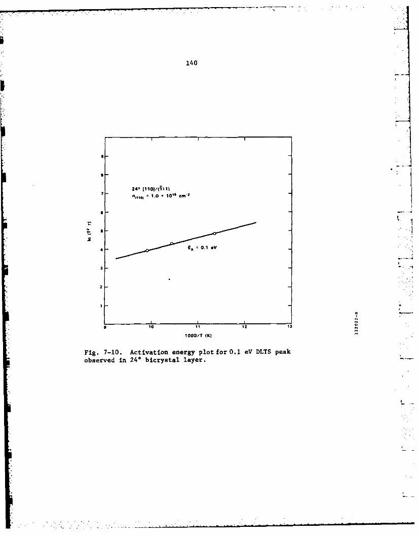
140
24- 11 1j
*10 10' 12m1
obevdi44 irsa layer.lV
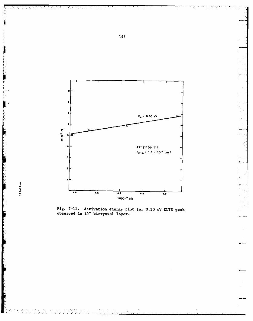
141
3-
454.6 4.7 4.8 4.9
1000/T (K)
Fig. 7-11. Activation energy plot for 0.30 eV DLTS peakobserved in 24* bicrystal layer.

7I
142
S S
24 10/11
a110 1. 06CP
3
2P
IS3637 . .
observed~24 in 4* icrsta laer

143
TABLE 7-3
ACTIVATION ENERGIES AND NORMALIZED PEAK HEIGHTSFOR DLTS SPECTRA OF GaAs TILT BOUNDARY SAMPLES
n(1I0) (cm- 3 ) EC - ET (eV) Normalized Peak Height (AC/C)
10 2.5 x 10¹⁵ 0.10 1.2 x 10- 4
0.33 4.0 x 10 -4
0.71 9.5 x 10⁻⁴
10 1.0 x 10¹⁵ 0.10 1.1 x 10- 3
0.30 2.2 x 10- 3
0.65 3.3 x 10- 3
24 1.0 x 10¹⁵ 0.10 2.8 x 10⁻³
0.30 1.0 x 10⁻³
0.67 1.1 x 10⁻²
30 1.0 x 10¹⁵ 0.63 2.5 x 10- 2
0.87 1.9 x 10⁻²
0* 2.5 x 1015 0.17 N.A.0.29 N.A.
*Schottky Contact

144
bulk of the grains and, thus, are not associated with the grain boundaries.
The energies of the traps in the 0* specimen are also consistent with
previously reported energies of bulk GaAs trap states.(1 15) There is no
conclusive evidence to identify the 0.87 eV trap observed in the 30* sample
with the grain boundary. However, its presence is consistent with the C-V
results and its high density relative to the other observed bulk states
suggests that it is a grain boundary state. It may be that this trap is
not observed in the other samples because their Fermi levels are pinned by
the grain boundary states at positions such that the peak associated with
this trap cannot be resolved in the DLTS spectra.
The DLTS results suggest that there are two discrete bands of states
associated with the grain boundary, located at about 0.65 and 0.9 eV below
the conduction band edge, and the density of these states at the grain --
boundary depends on the grain boundary structure. Fermi level pinning by
these bandgap states determines the electronic properties of GaAs grain
boundaries. This supports the GaAs defect state model proposed by Fan
et al.(5 8,5 9) These observations indicate that these grain boundary states
are intrinsic to the grain boundary structure. The fact that there are,
indeed, discrete bands of grain boundary states indicates that there is a
characteristic bonding defect structure associated with the grain boundary.
The 0.65 eV trap has not been observed in bulk GaAs. However, it has
been reported for many types of GaAs interfaces such as surfaces,(116)
heteroJunctions,(1 17) and GaAs-insulator interfaces.(1 18). Fermi level
pinning due to this level determines the electrical properties of such
interfaces.. 0 6,119,120) Grain boundary states with energies of EC - ET -
0.62 and 0.74 eV in GaAs have recently been reported.(6 3) These proposed

145
models are summarized graphically in figure 3-1. It is interesting to
note that the two grain boundary states reported here may be due to the
same bonding defects as the 0.65 and 0.90 eV bandgap states reportedly
associated with GaAs surfaces.(116)
The results presented in this section strongly suggest that the
intrinsic grain boundary structure influences the electronic properties,
that there is a characteristic bonding arrangement associated with the
grain boundary structure, and that the electronic states resulting from
these bonding defects are similar to those found at other types of GaAs
interfaces. However, it must be pointed out that there is some -
uncertainty associated with these interpretations due to several
experimental limitations. First, the exact parameters describing the
electronic band structure associated with the grain boundaries could not
be determined because of the lateral carrier concentration nonuniformities
in the bicrystal layers. These variations in donor density, inherent in
the overgrowth process, made the data interpretation difficult. Second,
it was not possible to analyze for the presence of extrinsic grain
boundary states, such as effects due to impurity segregation in the grain
boundaries. However, the behavior of the 0* baseline samples gave no
* indication of the presence of such effects; moreover, the S1O 2 overgrowth
stripe serves to keep substrate impurities out of the grain boundary by
acting as a diffusion barrier. However, defect states present at the
GaAs-SiO 2 interface may influence the grain boundary properties. Again,
the behavior of the 0* boundaries indicates such an effect is negligible.
There is only minimal annealing of the grain boundary structure since the
epitaxial growth temperature is only 720*C and post-growth heat treatment
* is confined to the alloying of the ohmic contacts. Whether these results

146
are representative of the behavior of grain boundaries in GaAs prepared by
other techniques is not known.
7.4 Implications for Grain Boundary Structure
The results of the J-V and C-V analysis show that the grain boundary
potential barrier height remains constant with increasing misorientation
angle for the [1101/(T1I) tilt boundaries. McPherson, et al.( 6 4) reported
a theoretical analysis of the relationship between misorientation angle
and barrier height for symmetric tilt boundaries in GaAs. This model
assumed the boundary to be composed of a dislocation array with the
dislocations having a Burgers vector of b - ao/2[110 ]. Their analysis,
based on trap states associated with dangling bonds along the length of
the dislocations, predicted a decrease in * with increasing e for e > 10.
This is contrary to the present experimental results. The geometric grain
boundary structure to which their theoretical analysis applies differs
from that of the prepared tilt boundaries only with respect to the
orientation of the grain boundary plane. Thus, the complete disagreement
of theory and the present experiments suggests that the dislocation
array/dangling bond model for grain boundary microstructure is not
appropriate for GaAs.
The DLTS analysis of GaAs grain boundaries reported in this thesis
and by other workers(6 3) has shown that discrete electronic states are
associated with the intrinsic grain boundary structure. This indicates
that a characteristic defect structure is associated with the grain
boundary. Such a defect structure results from a particular atomic
arrangement at the grain boundary interface. This is interpreted as the
result of reconstructed bonding leading to the formation of the stable

147
grain boundary microstructure. Such an interpretation is consistent with
the contemporary models of grain boundary microstructure discussed in
Chapter 3.
The actual microstructures of the tilt boundaries in the oriented
bicrystal layers were not determined in this research. However, drawing
on recent studies of grain boundaries in Ge and Si, a possible
microstructure for grain boundaires in GaAs is that illustrated in figure
3-3. In this proposed model, the grain boundary is composed of
microfacets along twin-related orientations and the bonding structure
consists of a periodic arrangement of 5, 6, and 7 member rings. This
results in bond length dilation and variations in bond angle. For GaAs,
this structure gives rise to like-atom bonds (Ga-Ga and As-As bonds) but
there are no associated dangling bonds. It is significant to note that
Ga-Ga and As-As bonds are analogous to missing As and Ga atoms,
respectively. Bandgap states associated with GaAs surfaces with energies
of EC -ET - 0.65 and 0.90 eV have been attributed, respectively, to
missing As and Ga atoms.(1 16) This result supports the concept that the
GaAs grain boundary states are related to a type of antisite defect
associated with like-atom bonds. Assuming the observed grain boundary
states are due to these bonding configurations, the results of the C-V
analysis indicate that the number of As-As bonds is twice that of Ga-Ga
bonds.
This proposed bonding arrangement would result from the formation of
the 5 and 7 member ring structures that have been found to exist at grain
boundaries in Ge and Si. Therefore, there is sufficient evidence to make
this a plausible model for the microstrcture of grain boundaries in GaAs
and other covalent semiconductors. This is not to say that dangling bonds

148
a do not exist at GaAs grain boundaries but that there is an alternative,
plausible atomic arrangement that is consistent with the experimental
results.
7. 5 Summary
The experimental analysis of the electronic properties of a series of
tilt boundaries having preselected structures in GaAs bicrystal layers has
been presented. The data indicate that the grain boundary potential
barrier height remains constant with changing misorientation angle. This
P- is consistent with Fermi level pinning by grain boundary states. The
density of grain boundary states, as determined from C-V analysis,
increases with e to a maximum value of approximately 2 x 1012 cm72 f or 0
in the range of 24 to 30% The rectification associated with majority
carrier transport also saturates in this range. DLTS analyses of highly
rectifying grain boundaries indicates that there are two discrete bands of
bandgap states associated with tilt boundaries in GaAs. These bands are
located at approximately EC - ET - 0.65 and 0.9 eV and are responsible for
the observed grain boundary properties.
0 The data are consistent with a model for the grain boundary
microstructure based on reconstructed bonding at the grain boundary
interface. A plausible bonding arrangement has been proposed. According
to this model the grain boundary states in GaAs may result from the
* periodic arrangement of like-atom bonds along the interface, as well as
dilated bond lengths and variations in bond angle.

149
8: Conclusion
8.1 Summary
This thesis presents the results of an investigation of the
electronic properties of grain boundaries in GaAs. The original objective
of this research was to investigate why grain boundaries in GaAs displayed
a range of electronic properties. In this context, it was demonstrated
that the grain boundary properties are determined by both the intrinsic
boundary structure and extrinsic compositional effects. However, this
work was taken much further by the development of a technique for the
preparation of grain boundaries having preselected structures. Through
the analysis of the properties of these grain boundaries, a relationship
between grain boundary properties and structure was demonstrated.
It is shown that the electronic band configuration associated with
grain boundaries is influenced by the grain boundary structure, reflecting
a direct relationship between the density of grain boundary states and the
misorientation parameters. The nature of the intrinsic grain boundary
bandgap states indicates that a characteristic defect structure is
associated with the bonding arrangement at the grain boundary interface.
A plausible model of the resulting atomic arrangement is presented.
The effect of grain boundaries on GaAs photovoltaic devices was
investigated and compared with electroluminescent properties. A variety
of grain boundary effects were observed. Cathodoluminescence analysis and
transmission electron microscopy were employed to investigate the origins
of these effects. Within the limits of applicable experimental
techniques, it is demonstrated that both structure and composition
influence the optoelectronic properties of grain boundaries in GaAs. Twin

150
boundaries were determined to have a minimal effect on GaAs optoelectronic
properties and devices.
A technique was developed for the growth of GaAs bicrystal epitaxial
layers containing grain boundaries having preselected structures. This
procedure was demonstrated by the preparation of a series of [1101 tilt
boundaries with a (TIl) boundary plane and misorientation angles ranging
from 0 to 30. The electronic properties of these grain boundaries were
investigated as a function of misorientation angle and carrier
concentration. The majority-carrier transport properties were found to be
consistent with a double-depletion-region model for the grain boundary
band structure. There is strong evidence that discrete bands of grain
boundary bandgap states are located at approximately 0.65 and 0.9 eV below
the conduction band edge. These states, also observed at other types of
GaAs interfaces, may be associated with Ga-Ga and As-As like-atom bonds.
The electrical transport properties of the GaAs tilt boundaries are
found to be inconsistent with a dislocation array/dangling bond model for
grain boundary structure. The presence of discrete bands of grain
boundary states indicates that a characteristic bonding defect structure
is associated with the grain boundary. This is interpreted as the result
of bond reconstruction at the grain boundary interface. A plausible
bonding configuration is proposed based on the formation of five, six, and
seven member rings along the grain boundary. This configuration results
in the like-atom bonds (or a related defect structure) in the III-V
systen

151
8.2 Suggestions for Future Work
The types of grain boundary structures that can be obtained using the
overgrowth technique should be useful for a variety of materials science
investigations. These include fundamental investigations of grain
boundary structure, properties, and kinetics. There are, however, several
areas into which this thesis work could be directly extended. For
instance, grain boundaries with identical structures could be prepared in
both p-and n-type layers and characterized to unambiguously determine the
influence of material type on grain boundary potential barrier height.
The range of misorientation angles could be extended and the properties of
high coincidence boundaries could be investigated. The effects of
individual well-characterized grain boundaries on solar cell performance
could be studied with the intention of developing techniques for grain
boundary passivation. High resolution transmission electron microscopy of
these tilt boundaries could be employed for fundamental studies of grain
boundary structures. In addition, such a study might be used to determine
the nature of the crystal defect structure associated with the bandgap
states that appear at many different types of GaAs interfaces. The
oriented bicrystal growth technique should be applicable to other grain
boundary orientations and other materials that exhibit lateral epitaxial
overgrowth.
IL

153
9: Appendices
9.1 Appendix 1: Deep Level Transient Spectroscopy
Deep level transient spectroscopy (DLTS)(12 1- 124 ) is a technique for
the investigation of semiconductor bandgap states by the analysis of a
diode capacitance transient. It has been applied to the measurement of
trap concentration, activation energy, and capture cross section. The
usual configuration for DLTS makes use of either a p-n junction or
Schottky barrier diode. As discussed earlier, it has also been applied to
the study of semiconductor grain boundary states by making use of theL.
inherent diode properties of these defects. The basic DLTS technique is
described in this section.
Application of the DLTS technique to bulk semiconductors involves
measurement of the high frequency capacitance of either a junction diode
or a Schottky barrier diode after a transient bias pulse. The technique
will be explained by considering an asymmetric p+n junction (p doping is
much greater than n doping) with an applied reverse bias at a quiescent
equilibrium. Associated with the junction is a space charge region of
width112
2Cor [Vbi + a ]L , (IX-)eN+ Ib
where toCr is the dielectric constant of the semiconductor, Vbi is the
built-in voltage of the junction, e is electronic charge, Va is an applied
reverse bias voltage, and X+ is the concentration of positive charge in
the space charge region. The capacitance of the junction having area A is
C - CoCrA (IX-2)d
Thus C varies directly with charge concentration and inversely with
reverse bias voltage. The important features are that d can be adjusted
4 . , . . - - . . .
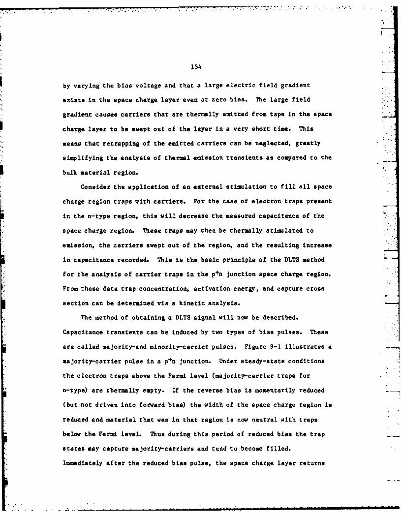
154
by varying the bias voltage and that a large electric field gradient
exists in the space charge layer even at zero bias. The large field
gradient causes carriers that are thermally emitted from taps in the space
charge layer to be swept out of the layer in a very short time. This
means that retrapping of the emitted carriers can be neglected, greatly
simplifying the analysis of thermal emission transients as compared to the
bulk material region.
Consider the application of an external stimulation to fill all space
charge region traps vith carriers. For the case of electron traps present
in the n-type region, this will decrease the measured capacitance of theL
space charge region. These traps may then be thermally stimulated to
emission, the carriers swept out of the region, and the resulting increase
in capacitance recorded. This is the basic principle of the DLTS method -
f or the analysis of carrier traps in the p+n junction space charge region.
From these data trap concentration, activation energy, and capture cross
section can be determined via a kinetic analysis.
The method of obtaining a DLTS signal will now be described.
Capacitance transients can be induced by two types of bias pulses. These
are called majority-and minority-carrier pulses. Figure 9-1 illustrates a
majority-carrier pulse in a p+n junction. Under steady-state conditions
the electron traps above the Fermi level (majority-carrier traps for
n-type) are thermally empty. If the reverse bias is momentarily reduced
(but not driven into forward bias) the width of the space charge region is
reduced and material that was in that region is now neutral with traps
below the Fermi level. Thus during this period of reduced bias the trap
states may capture majority-carriers and tend to become filled.
Immediately after the reduced bias pulse, the space charge layer returns

155
ELECTRON TRAP
P N UIESCENT REVERSE BIS
cvREDUCED BIAS PULSE
t BlUE
TRANSIENT / W TR
10 TEPERATUREOBSERVE TRAPS
JUNCTION N THIS REGION
Fig. 9-1. Schematic illustration of a majority carrier fillingpulse for a p~n Junction. Configuration before, during; andafter pulse from top to bottom. Insert shows the capacitancetransient at different temperatures [Lang (121)].
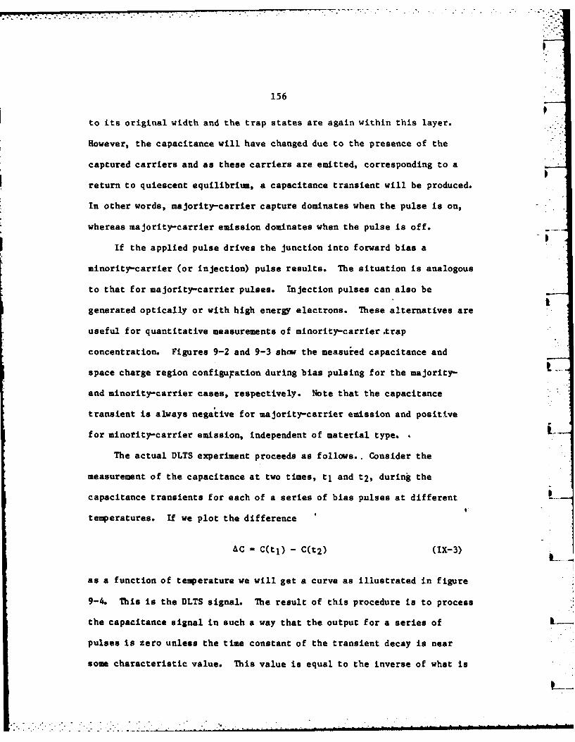
156
to its original width and the trap states are again within this layer.
However, the capacitance will have changed due to the presence of the
captured carriers and as these carriers are emitted, corresponding to aI
return to quiescent equilibrium, a capacitance transient will be produced.
In other words, majority-carrier capture dominates when the pulse is on,
whereas majority-carrier emission dominates when the pulse is off.
If the applied pulse drives the junction into forward bias a
minority-carrier (or injection) pulse results. The situation is analogous
to that for majority-carrier pulses. Injection pulses can also beft
generated optically or with high energy electrons. These alternatives are
useful for quantitative measurements of minority-carrier ,trap
concentration. Figures 9-2 and 9-3 show the measured capacitance and
space charge region configuFation during bias pulsing for the majority-
and minority-carrier cases, respectively. Note that the capacitance
transient is always negative for majority-carrier emission and positive
for minotity-carrier emission, independent of material type.
The actual DLTS experiment proceeds as follows., Consider the
measurement of the capacitance at two times, t1 and t2, during the
capacitance transients for each of a series of bias pulses at different
temperatures. If we plot the difference
AC - C(t) - C(t2 ) (IX-3)
as a function of temperature we will get a curve as illustrated in figure
9-4. This is the DLTS signal. The result of this procedure is to process
the capacitance signal in such a way that the output for a series of
pulses is zero unless the time constant of the transient decay is near
some characteristic value. This value is equal to the inverse of what is
, .. . .... . . _ ,, - _ , . .. . . . . . . . . . . . . .

157
® 'MAJORITYCARRIER PULSE"
two
I&C-
(!) QUIESCENT I -LREVERSE BIAStI
TRANSIENT -
"I DUE TO, THERMAL
EMISSION® BEGINNING t>"
OF TRANSIENTtr-O.
Fig. 9-2. Schematic illustration of capacitance transient for iso-thermal emission from a majority carrier trap. Inserts show the p+njunction configuration at various times during the transient [Lang(121) ].
.4
'1

158
( ) INJECTION .
PULSEt-O
) DECAY OFTRANSIENT
t DUE TO//C THERMAL L
•g EMISSION
® QUIESCENTREVERSE_ -,BIASt<O 0
O1 BEGINNINGOF TRANSIENTt= O +
Fig. 9-3. Schematic illustration of capacitance transient for iso-thermal emission from a minority carrier trap. Inserts show thep+n junction configuration at various times during the transient
[Lang (121)].

159
II
-It_ _TIM --- - - -
Fi.94 eeain;fteDT inlbsapln the caitne rasnt ttw
gae boca Iehd(an 11]
160
called the "rate window" and is determined by the values of tj and t 2 .
This is the basic concept behind the DLTS technique. The plot of the
values of AC obtained in this way as a function of temperature and using a
set rate window is called the DLTS spectrum.
For this sampling condition, the trap concentration in the n-type
region is given by
NT - 2(AC/C) (ND - NA) , (IX-4)
where AC is as defined in equation (IX-3), C is the equilibrium
configuration capacitance, and ND and NA are the donor and acceptor ..
concentrations, respectively, in the n-type region. Thus the trap density
is proportional to AC/C. It is assumed that the capacitance transient
decays exponentially with time and is characterized by a relaxation time T -
such that
C(t) - e(-t Ir) . (IX-5)
For an electron trap in the n-type region
T TV4 exp (AE/kT) L exp (hE/kT) , (1-6)
where gT is the degeneracy of the trap level, aT is the trap cross
section, <v> is the mean electron thermal velocity, Nc is the density of
states in the conduction band, and AE is the energy difference between the
conduction band edge and the trap level. A similar expression holds for
minority carrier traps.
It is evident from equation (IX-6) that AE can be obtained from the
slope of a plot of In(T2 T) versus reciprocal temperature. The sampling
conditions described above can be obtained by processing the measured
capacitance transient with a dual gated boxcar averager. The output of

161
this instrument is exactly the signal AC given by equation (IX-3). For
this condition the value of T used to obtain a particular spectrum is
=tl - t2. (Ix-7)tn(tl/t 2)
The capacitance transient can also be processed using a lock-in amplifier.
For this method the obtained signal is the correlation of the exponential
transient with the reference waveform of the lock-in amplifier. For a
sine wave reference signal of frequency f, the value of T is given by
- 0.424/f . (IX-8)
The basic DLTS technique has been described based on the measurement Lof p+n diode capacitance. For analysis of grain boundary states the
technique is modified in that there is no bias applied at the equilibrium.
configuration. In addition, it is not possible to empty states below theL
equilibrium Fermi level since a bias pulse across the grain boundary
always results in a filling reverse bias condition. Thus DLTS analysis of
the grain boundary states by using the grain boundary potential barrier as
the charge separation mechanism only allows the study of traps present
above the Fermi level. However, the use of this configuration is required
because it confines the depletion region to the vicinity of the spatially
localized grain boundary states.
9.2 Appendix 2: Transmission Electron Microscopy Sample Preparation
Most GaAs TEM samples used in this thesis research were prepared by
standard chemical jet etching(1 25) using a etching solution of 40 Rdc:
4 H202: I H20. In the course of this work, an anodic dissolution
technique has been developed for the thinning of relatively large,
selected areas of single crystal or polycrystalline GaAs to prepare

162
self-supporting uniformly thin foils for TEM examination. (12 6) This
technique is described in this section.
To use the anodic dissolution technique, a GaAs wafer is first lapped
with 2 Pm grit, mechanochemically polished in Clorox to a thickness of
80-100 Pm, and diamond sawed into square samples 2.5 mm on a side. The
wafers used in this investigation were doped with Zn at concentrations of
p - 1018 cm-3 . A sample selected for thinning is electroplated on one
face (except for the region to be examined) with a layer of Au about 5 um
thick, then heated to 300*C for 1 sec to form an ohmic contact(127). A Pt
wire is attached to the Au contact with conductive adhesive, and the
sample is mounted contact-side-down on a glass slide with transparent wax.
The area to be thinned is defined by covering the exposed surface with wax
except for a circle, typically about 0.5 m in diameter, opposite the
region not plated with Au. The sample configuration is shown
schematically in figure 9-5. Dissolution proceeds from the exposed
surface toward the contact surface.
The sample form the anode of an electrochemical cell with a large
area Pt-mesh cathode. The electrolyte is the disodiu- salt of 0.IM
4-5-dihydroxy-m-benzee-disulfonic acid, which is very similar in
composition to the Tiron solution used by Faktor and Stevenson(12 8) for
characterization of GaAs by anodic dissolution but is preferred because of
its lower cost and better availability. Measured polarization curves for
the two solutions are virtually identical. Dissolution is performed at a
constant current density of 15 mA/cm 2 with an etch rate of approximately
0.3 Pm/min, so that 4 to 5 hr is usually required to achieve the desired
sample thickness. It was observed that lower currents delineate crystal

163
TRAN SPARENTWAX
LTHIN FOIL
'01 0
-ooo Au CONTACT
GRAINBOUNDARI ES
IN GaAs
Fig. 9-5. Schematic diagram showing a GaAs sample mounted foranodic dissolution.

164
defects while higher currents tend to result in nonuniform etching
unrelated to such defects.
The transmission of a low power (2 uW) He-Ne (6328A) laser through
the foil is monitored to determine when the dissolution process should be
terminated. To reduce background noise the laser beam is chopped
mechanically at 400 Hz, and the transmitted radiation is detected by using
a lock-in amplifier to measure the output of an Si photodiode across a Ifl
load resistor. the circuit of the electrochemical cell is interrupted as
soon as transmission is detected, which occurs when the foil is about
2000 A thick. The measurements are made intermittently, and the laser is
shuttered between measurements, since the dissolution rate is increased by
light so that continuous laser exposure would therefore result in
nonuniform thinning.
During the dissolution process the GaAs surface becomes coated with a
brown-black film, which has been shown by Auger analysis to be composed of
As and 0 without detectable Ga. Unlike films formed by anodic oxidation
of GaAs, this coating is not soluble in HC1. To remove the coating, after
dissolution is complete the GaAs surface is anodically oxidized in a
tartaric acid/propylene glycol solution(12 7 ,1 29) and the oxide formed is
dissolved in dilute HCL. The sample is then removed from the glass slide
by dissolving the wax and cleaned in successive acetone and methanol
baths.
Self-supporting thin foils of both single crystal and polycrystalline
GaAs have been prepared by the procedure described. The single crystal
samples usually can be thinned uniformly without perforation. Figure 9-6
is a transmission optical micrograph of such an unperforated sample with a
thin region approximately 0.2 mm2 in area and 2000 A thick. Although the
1

165
.- U
', 0.2m..
Fig. 9-6. Transmission optical micrograph of a single crystalGaAs foil.
166
transmitted intensity varies strongly within this region, TEM examination
shows that the foil is essentially uniform in thickness, and Nomarski
contrast microscopy of the etched surface reveals the same features as the
optical transmission micrograph. Therefore, we attribute the observed
variation in transmitted light intensity to scattering resulting from the
roughness of the foil surface.
9.3 Appendix 3: Capacitance-Voltage Analysis Technique
This section describes a technique for the self-consistent analysis
of the grain boundary C-V characteristics to obtain the band structure
associated with a general grain boundary, as illustrated in figure 7-1.
The technique is described through the presentation of the analysis of the
C-V characteristic of a 30* grain boundary prepared by lateral epitaxial
overgrowth. The technique does not provide exact values for the
parameters describing the band structure but gives values that fit the C-V
data and can therefore be used to obtain the actual density of grain
boundary states filled at zero-bias.
As described in Chapter 7, the grain boundary capacitance, C, for an
applied voltage Va is given by(IX-9)
1/2 + 1/2 + 1/2
where A is the grain boundary area, e is the magnitude of electronic
charge, co is the permitivity of free space, and er is the relative
dielectric constant. All other parameters are defined in figure 7-1. LetV
V1 - *1/e and V2 = *2/e. Then the above equation can be written
167
as(Ix-lo)
1/21/2 1/21A 2V1 + Va +( V2-
2 eor N l2
For the case when Va<<VI we can use the approximation that
1/2
I.V ( + V) 1/ (i 1/2 +
Equation (IX-lO) then becomes
(IX-12)
1/2 1/2 12A { 2( !V 2 + / 2 ! a 1 / 2
1/2 1/2
-A+ ( Va (Ix-13)Co 2eeoe~r ) (1 ) V
where Co is the zero-bias capacitance.
For e = 1.602 x 1O-19 coul,
Co 8.854 x 10- 14 F/cm,
and er 12.54,
this equation can be written as
A _ A + [1.68 x 10⁵ Va (IX-14)"C CO (VN)1/2
where A is in cm2 , C and Co are in farads, V1 and Va are in volts, and N'
is in cm- 3. This equation shows that the product (VIN1) can be obtained - ,
from a plot of A/C versus reverse bias voltage.
I.

168
Now consider the case when Va > V1 and V2. For this condition
equation (IX-10) can be approximated as
A 2 1/2 1 + V 1/2 (IX-15)C coer / 2
This can be reqritten as(IX-16)
2 1/2 1/22A - 1 \2 / 2 1/ + /2 )(V2\ 2 Va
A C ecocr N2 (eocr N2 ecoer )N
or
(IX-17)
2 1/26.71 x 1015 (A)(2 + 1.12 x 1031 .31 x 1031
C 2 ~N 2 N1
This is a complicated expression but, since the variation of A/C with Va
is negligible compared to that of (A/C)2 , equation (IX-17) indicates that
N1 can be obtained from the slope of a plot (A/C)2 versus Va. Thus N1 can
be obtained from capacitance measurements for large Va and the product
(VIN I) can be obtained from data taken at small applied voltages.
A self-consistent solution for the band structure associated with the
grain boundary can be obtained using this analysis of the C-V
characteristics for reverse bias of the grain that shows the most rapid
decrease in capacitance. Figure 9-7 shows A/C and (A/C)2 plotted as a
function of applied voltage for a 30* tilt boundary with n(110) - 1.0 x
i05 cm 3. The slope of A/C versus Va is obtained from the data where Va
< 0.2 volts. The slope of (A/C)2 versus Va is obtained for data where 0.7

169
'47
A/
4-
u SLOPEs 9.8 x 10¹⁴
fl(I 1 1.0 x10¹¹ CM-3
0.1 0.2 0.3 0.4 0.5 0.6 0.7 0.8 0.9 1.0VOLTAGE (VI
2 2Fig. 9-7. A/C and A /C versus bias voltage for a 300GaAs bicrystal layer.

170
, Va 4 1.0 V. The slope of (A/C)2 versus Va was observed to be fairly
constant up to about 2.0 V where it changes rapidly due to carrier
concentration nonuniformities. From the measured slopes
NIVI - 1.68 x 10¹⁵ - 1.24 x 10¹⁶ Vcm73
1.51 x 10⁷
and
N - 1.12 x 1031 - 1.14 x 1016 cm- 3
9.80 x 10¹⁴
Thus, V I 1.09 V and *I - 1.09 eV. Refering to figure 7-1, the position
of the Fermi level below the conduction band edge is given by
8 E EF kT In NC (IX-18)C F [ND -NA
where Nc = 4.7 x 101 7 cm -3 is the density of states in the conduction band
of GaAs. Thus(IX-19)
61 kT tn [ - 0.025 in [ 4.7 1017 J-0.093 eVN lJL 1.14 x 10¹⁶
The zero-bias grain boundary capacitance is given by
A .3.35 x 1015 L 1 21 •x-20)o)1/2 + ! j2 /2]
For this sample A/Co - 4.87 x 107 cm2 F- I and, thus,
{, 1/2 1/2
V( I 1/ 1.09 -" 9.78 x 10- 9
NI\ 1.14 x 10¹⁶

171
Substituting these values into equation (IX-20) we obtain
4.87 x 10⁷ 3.35 x 10¹⁵ [9.78 x 10- 9 +()J/
or
V2 -2.26 10i-17 N2 .(IX-21)
The position of the fermi level at the grain boundary is given by
6GB 1 41 82 +42 (IX-22)
Substituting into this relation and using equation (IX-18) yields
1.09 + 9.3 x 1o .2 o-7N 0.025 In [. x 1017J
or(IX-23)
1.11 x 10¹⁵ £n f4.7 x 1 205.31706
Numerical solution of equation (IX-23) gives the value of N2 as
N2 - 4.98 x 1016 cm 3
Using equation (IX-21)
02- (2.26 x 10⁻¹⁷)(4.98 x 10¹⁶) 1.13 eV
From equation (1X-22)
82 -1.09 + 0.093 -1.13 -0.053 eV
and
8B 1. 18 eV
.Le
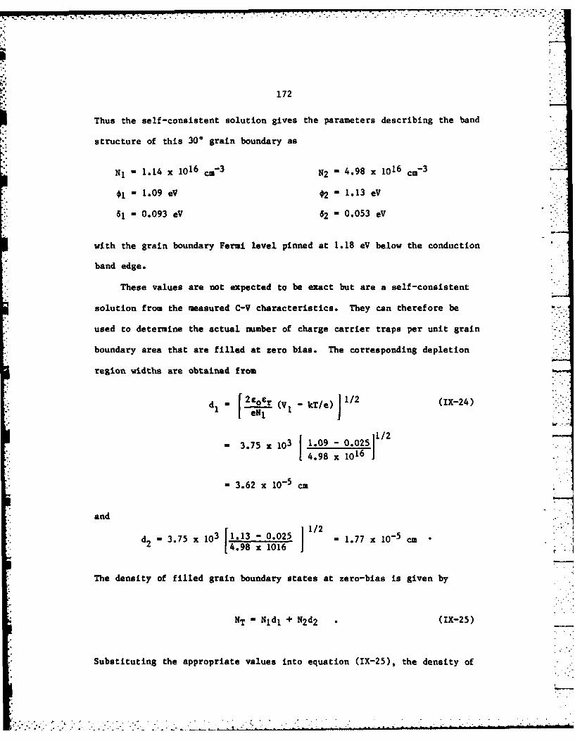
- - .- -,
172
Thus the self-consistent solution gives the parameters describing the band
structure of this 300 grain boundary as
N1 - 1.14 x 101 6 c. 3 N2 - 4.98 x 10¹⁶ ci-3
41 - 1.09 eV #2 - 1.13 eV
81 - 0.093 eV 62 - 0.053 eV
with the grain boundary Fermi level pinned at 1.18 eV below the conduction
band edge.
These values are not expected to be exact but are a self-consistent
solution from the measured C-V characteristics. They can therefore be
used to determine the actual number of charge carrier traps per unit grain
boundary area that are filled at zero bias. The corresponding depletion
region widths are obtained from
" 2er - T/) 1/2 (X24)eN1
- 3.75 x 1 3 1.09 - 0.025 1/2
1,4.98 x
- 3.62 x 10- 5 cm
and ,
2 1/2d 3.75x 1.13- 0.025 -1.77 x 10- 5 cm
4.98 x 10¹⁶ 1
The density of filled grain boundary states at zero-bias is given by
NT - Nldl + N2d2 . (IX-25)
Substituting the appropriate values into equation (IX-25), the density of

173
filled trap states for this 30* grain boundary at zero-bias is
NT -1.29 x 10⁻¹² cm-2
*1Z

175
BIBLIOGRAPHY
1. D. M. Chapin, C. S. Fuller, and G. L. Pearson, J. Appl. Phys. 25,676 (1954)
2. H. J. Hovel, in Solar Cells, Vol. 11 of Semiconductors and
Semimetals, R. K. Willardson and A. C. Beer (Academic, New York,1975).
3. S. M. Sze, Physics of Semiconductor Devices, (Wiley, New York,
1971).
4. J. C. C. Fan, Tech. Review 80, 2 (1978).
5. W. T. Read, Jr. and W. Shockley, Phys. Rev. 78, 275 (1950).
6. J. Hornstra, J. Phys. Chem. Solids 5, 129 (1958). -
7. R. Landauer, Phys. Rev. 94, 1386 (1954).
8. V. Celli, A. Gold, and R. Thompson, Phys. Rev. Lett. 8, 96 (1962).
9. V. Heine, Phys. Rev. 146, 568 (1966).
10. W. Guth, Phys. Stat. Sol. (b) 51, 143 (1972).
11. R. Labusch and W. Schroter, Inst. Phys. Conf. Ser. No. 23, 56 (1975).
12. W. Barth, K. Elsaesser, and W. Guth, Phys. Stat. Sol. (a) 34, 153(1976).
13. E. Kamieniecki, J. Phys. C 9, 1211 (1976).
14. E. Kamieniecki, J. de Physique 40, C6-87 (1979).
15. E. Elbaum, Solar Cells 1, 216 (1980). -
16. W. Shockley, Phys. Rev. 91, 228 (1953).
17. L. M. Frass and K. Zanio, Hughes Aircraft Co. Research Report 521,August 1978, unpublished.
18. L. L. Kazmerski, Solid State Electron. 21, 1545 (1978).
19. L. M. Frass, J. Appl. Phys. 49, 871 (1978).
20. C. H. Seager, D.S. Ginley, and J. D. Zook, Appl. Phys. Lett. 36, 831(1980).
21. P. H. Robinson and R. V. D'Aiello, Appl. Phys. 39, 63 (1981).
22. S. K. Ghandi, J. M. Borrego, D. Reep, Y-S. Hsu, and K. P. Pande, Appl.Phys. Lett. 34, 699 (1979). • .
"'"" " " " •- " " " "- . ... :_ _. . _ . 1

-~~~~~ 777. -~~.
176
23. G. L. Pearson, Phys. Rev. 76, 459 (1949).
24. W. E. Taylor, N. H. Odell, and H. Y. Fan, Phys. Rev. 88, 867 (1952).
25. W. Schockley, Phys. Rev. 56, 317 (1939).
26. A. F. Tweet, Phys. Rev. 96, 828 (1954).
27. A. G. Tweet, Phys. Rev. 99, 1182 (1955).
28. B. Reed, 0. A. Weinreich, and H. F. Matare, Phys. Rev. 113, 454 (1959).
29. R. K. Mueller, J. Phys. Che.. Solids 8, 157 (1959).
30. H. F. Matare, J. Appi. Phys. 30, 581 (1959).
31. Y. Matukura and S. Tanaka, J. Phys. Soc. Japan 16, 833 (1961).
32. R. K. Mueller, J. Appl. Phys. 32, 635 (1961). P
33. R. K. Mueller, J. Appl. Phys. 32, 640 (1961).
*34. P. Handler and W. Ma Portnoy, Thy.. Rev. 116, 516 (1959).
35. A. Broniatowaki and J-C. Bourgoin, Phys. Rev. Lett. 48, 424 (1982). -
36. Y. Matukura, 3. Phys. Soc. Japan 16, 842 (1961).
37. T. I. Kamins, J. Appl. Phys. 42, 4357 (1971).
38. H. C. Card and E# S. Yang, IEEE Trans. Electron Devices ED-24, 397(1977).
*39. C. H. Seager and T. G. Caitner, J. Appl. Phys. 49, 3879 (1978).
40. C. H. Seager, G. E. Pike, and D. S. Ginley, Phys. Rev. Lett. 43, 532(1979).
*41. G. E. Pike and C. H. Seager, J. Appl. Phys. 50, 3414 (1979).
*42. C. H. Seager and G. E. Pike, Appl. Phys. Lett. 35, 709 (1979); anderratum, Appl. Phys. Lett. 37, 251 (1980).
*43. C. H. Seager and G. E. Pike, Appl. Phys. Lett. 37, 747 (1980).
*44. C. H. Seager, J. Appl. Phys. 52, 3960 (1981).
45. J. Martinez, A. Criado, and J. Piqueras, J. Appl. Phys. 52, 1301(1981).
46. G. H. Schwuttke, K. Yang, and T. F. Ciezek, J. Cryst. Growth 43, 329(1978).

177
47. D. Helmreich and H. Seiter, Proceedings of the 1979 European
Photovoltaic Solar Energy Conference, Berlin, West Germany, (1979).
48. D. Redfield, Appl. Phys. Lett. 38, 174 (1981).
49. L. J. Cheng and C. M. Shyu, in Semiconductor Silicon, eds. H. R. Huff,R. J. Kreiger and Y. Takeishi, (Electrochemical Society, Pennington,New Jersey, 1981), p. 390.
50. C. M. Wu and E. S. Yang, Appl. Phys. Lett. 40, 49 (1982).
51. D. Redfield, Appl. Phys. Lett. 40, 163 (1982).
52. L. L. Kazmerski, J. Vac. Sci. Tech. 20, 423 (1982).
53. H. J. Leamy, R. C. Frye, K. K. Ng, C. K. Celler, E. I. Povilonis, andS. M. Sze, Appl. Phys. Lett. 40, 598 (1982).
54. W. Hwang, H. C. Card, and E. S. Yang, Appl. Phys. Lett. 36, 315 t(1980).
55. J. J. J. Yang, P. D. Dapkus, R. D. Dupuis, and R. D. Yingling, J. Appl.Phys. 51, 3794 (1980).
56. H. J. Cohen, M. D. Paul, D. L. Miller, J. R. Waldrop, and J. S. Harris,
Jr., J. Vac. Sci. Tech. 17, 899 (1980).
57. L. L. Kazmerski and P. J. Ireland, J. Vac. Sci. Tech. 17, 525 (1980).
58. J. C. C. Fan, R. L. Chapman, J. P. Donnelly, G. W. Turner, and C. 0.Bozler, in Laser and Electron-Beam Solid Interactions and MaterialsProcessingI eds, J. F. Gibbons, L. D. Hess, and T. W. Sigmon,(North=Holland, New York, 1981), p. 261.
59. J. C. C. Fan, to be published in the Procedings of the Symposium onPolycrystalline Semiconductors, Perpignan, France, August 1982.
60. M. J. Cohen, J. S. Harris, Jr., and J. R. Waldrop, Inst. Phys. Conf.Ser. 45, p. 263.
61. C. H. Seager and G. E. Pike, Appl. Phys. Lett. 40, 471 (1982).
62. M. Spencer, R. Stall, L. F. Eastman, and C. E. C. Wood, J. Appl. Phys. L50, 8006 (1979).
63. H. G. Spencer, W. G. Schaff, and D. K. Wagner, in Grain Boundaries inSemiconductors, eds. H. J. Leamy, G. E. Pike, and C. H. Seager(NorthHolland, New York, 1982), p. 125.
64. J. W. McPherson, G. Filatovs, E. Stefanakos, and W. Collis, J. Phys.Chen6 Solids 41, 747 (1980).
65. J. W. McPherson, W. Collis, E. Stefanakos, A. Safavi, and A. Abul-Fadl,J. Electrochem. Soc. 127, 2713 (1980).

I . . .
178
66. W. Siegel, G. Kuhnel, and E. Ziegler, Phys. Stat. Sol. (a) 64, 249
(1981).
67. C. H. Seager and D. S. Ginley, Appl. Phys. Lett. 34, 337 (1979).
68. D. R. Campbell, Appl. Phys. lett. 36, 604 (1980).
69. C. II. Seager and D. S. Ginley, J. App.. Phys. 52, 1050 (1981).
70. C. H. Seager, D. J. Sharp, J. K. G. Panitz, and R. V. D'Aiello, J. Vac.Sci. Tech. 20, 430 (1982).
71. H. W. Lam, Appl. Phys. Lett. 40, 54 (1982).
72. G. W. Turner, J. C. C. Fan, and J. P. Salerno, U.S. Patent SerialNo. 223,768.
73. G. W. Turner, J. C. C. Fan, R. P. Gale, and 0. Hurtado, Proceedings ofthe 14th IEEE Photovoltaic Specialists Conference, 1980 (I-EEE, NewYork, 1980), p. 1530.
74. T. L. Chu, S. S. Chu, C. L. Lin, Y. C. Tzeng, L. L. Kazmerski, and P.J. Ireland, J. Electrochem. Soc. 28, 855 (1981).
75. W. T. Read, Jr., Dislocations in Crystals, (McGraw-Hill, New York,1953), p. 31, Chapters 11, 12.
76. J. M. Burgers, Proc. Phys. Soc. (London) 52, 23 (1940).
77. W. L. Bragg, Proc. Phys. Soc. (London) 52, 54 (1940).
78. W. T. Read and W. Shockley, Phys. Rev. 78, 275 (1950).
79. W. Bollmann, Crystal Defects and Crystalline Interfaces(Springer-Verlag, New York, 1970), Chapter 12.
80. R. W. Balluff 1, Grain Boundary Structure and Segregation, inInterfacial Segregation (ASH, Metals Park, Ohio, 1979), p. 193.
81. Grain Boundary Structure and Kinetics, ed. R. W. Balluffi (ASH, MetalsPark, Ohio, 1980).
82. P. R. Howell, et al., J. Micros. 107, 155 (1976).
83. H. Gleiter, Act&. Metal.. 18, 117 (1970).
84. H. Sautter, H1. Gleiter, and G. Baro, Acta. Metal.. 25, 40 (1977).
85. 0. L. Krivanek, S. Isoda, and K. Kobayashi, Phil Meg. 36, 931 (1977).
86. A. Bourret and J. Desseaux, Phil Kag. A19, 405 (1979).
87. A. Bourret and J. Desseawc, Phil Meg. M39, 413 (1979).

179
88. A. Bourret, Inst. Phys. Conf. Ser. 60, 9 (1981).
89. J-J. Bacmann, G. Silvestre, M. Petit, and W. Bollmann, Phil Mag. A43,189 (1981).
90. W. Bollmann, G. Silvestre, and J-J. Bacmann, Phil. Hag. A43, 201(1981).
91. A-M. Papon, M. Petit, G. Silvestre, and J-J. Bacmann, in GrainBoundaries in Semiconductors eds. H. J. Leamy, G. E. Pike, and C. H.Seager (North-Holland, New York, 1982), p. 27.
AL92. D. Viachavas and R. C. Pond, Inst. Phys. Conf. Ser. 52, 195 (1980).
93. C. B. Carter, H. Poll, D. G. Ast, and S. L. Sass, Phil. Hag. A43, 441(1981).
94. C. B. Carter, J. Rose, and D. G. Ast, Inst. Phys. Conf. Ser. 60, 153 L(1981).
95. C. Fontaine and D. A. Smith, Appi. Phys. Lett. 40, 153 (1982).
96. B. Cunningham, H. Strunk, and D. G. Ast, Appi. Phys. Lett. 40, 237(1982).
97. B. Cunningham and D. Ast, in Grain Boundaries in Semiconductors, eds.H. J. LeauzV, G. E. Pike, and C. H. Seager (North-Holland, New York,1982), p. 21.
98. C. Fontaine and D. A. Smith, in Grain Boundaries in Semiconductors,eds. H. J. LeauV, G. E. Pike, and C. H. Seager, (North-Holland, NewYork, 1982), p. 39.
99. C. B. Carter, in Grain Boundaries in Semiconductors, eds. H. J. Leamy,G. E. Pike, and C. H. Seager, (North-Holland, New York, 1982), p. 39.
100. S. M. Sze, Physics of Semiconductor Devices (New York: Wiley, 1969),p. 640.
101. S. Kamath and G. Wolff, Final Tech. Rep. AFAPL-TR-78-76, Jan. 1979.
102. G. W. Turner, J. Co C. Fan, and J. P. Salerno, Solar Cell 1, 261(1980).
103. D. A. Cusano, Solid State Comisin. 21, 352 (1964).
104. J. Vaughan, Ph. D. Thesis, M.I.T. (1981), unpublished.
105. D. B. Wittry and D. F. Kyser, J. Appl. Phys. 38, 375 (1967).
106. C. 0. Bozier, J. C. C. Fan, and R. W. McClelland, Inst. Phys. Conf.Ser. No. 45, 429 (1979).

180
107. F. W. Tausch, Jr. and A. G. Lapierre, III, J. Electrochem. Soc. 112,706 (1965).
108. R. W. McClelland, C. 0. Bozler, and J. C. C. Fan, Appl. Phys. Lett.37, 560 (1980).
109. C. 0. Bozler, R. W. McClelland, and J. C. C. Fan, Inst. Phys. Conf.Ser. No. 56, 283 (1981).
110. C. 0. Bozler, R. W. McClelland, and J. C. C. Fan, IEEE Electron Dev.Lett. EDL-2, 203 (1981).
111. C. 0. Bozler, R. W. McClelland, J. P. Salerno, and J. C. C. Fan, J.Voc. Sci. and Technol. 20, 720 (1982).
112. P. Vohl, C. 0. Bozler, R. W. McClelland, A. Chu, and A. J. Strauss, J.Cryst. Growth 56, 410 (1982).
113. W. R. Runyan, Semiconductor Measurements and Instrumentation(McGraw-Hill, New York, 1975), p. 88.
114. S. M. Sze, Physics of Semiconductor Devices (Wiley, New York, 1969),Chapter 8.
115. G. M. Martin, A. Mitonneau, and A. Mircea, Electronics Lett. 13, 191(1977).
116. W. E. Spicer, P. W. Chye, P. R. Skeath, C. Y. Su, and I. Lindau, J.Vac. Sci. Technol. 16, 1422 (1979).
117. S. R. McAfee, D. V. Lang, and W. T. Tsang, Appl. Phys. Lett. 40, 520
(1982).
118. T. E. Kazior, Ph.D. Thesis, M.I.T. (1982), unpublished.
119. W. E. Spicer, P. Pianetta, I. Lindau, and P. W. Chye, J. Vac. Sci.Technol. 14, 885 (1977).
120. W. E. Spicer, P. W. Chye, C. M. Garner, I. Lindau, and P. Pianetta,Surf. Sci. 86, 763 (1979).
121. D. V. Lang, J. Appl. Phys. 45, 3023 (1974).
122. L. C. Kimerling, I.E.E.E. Trans. Nuc. Sci. NS-23, 1497 (1976).
123. G. L. Miller, D. V. Lang, and L. C. Kimerling, in Annual Review ofMaterials Science vol. 7, eds. R. A. Huggins, R. H. Bube, and D. A.Vermilyea (Annual Reviews, Palo Alto, 1977), p. 377.
124. D. S. Day, M. Y. Tsai, B. G. Streetman, and D. V. Lang, J. Appl.
Phys. 50, 5093 (1979).
125. G. R. Booker and R. Stickler, Br. J. Appl. Phys. 13, 446 (1962).

181
126. J. P. Salerno, J. C. C. Fan, and R. P. Gale, J. Electrochem. Soc. 128,1162 (1981).
127. J. C. C. Fan, C. 0. Bozler, R. L. Chapman, Appl. Phys. Lett. 32, 390(1978).
128. M. M. Faktor and J. L. Stevenson, J. Electrochem. Soc. 125, 621(1978).
129. H. Hasegawa and H. L. Hartnagel, J. Electrochem. Soc. 123, 712(1976).
I

RD-A144 358 ELECTRONIC PROPERTIES OF GRAIN BOUNDARIES IN GAAS: A 3/3STUDY OF ORIENTED B!.. (U) MASSACHUSETTS INST OF TECHLEXINGTON LINCOLN LAB J P SALERNO ET AL. 10 MAY 84
UNCLASSIFIED TR-669 ESD-TR-83-066 F19628-80-C-0002 F/G 20/2 NL
Em

rrr-r-6 w-rrr 11.2 ----
QF
I 6 1220
I
1l.25 14 1.6
MICROCOPY RESOLUTION TEST CHART
NATIONAL BUREAU OF STANDARDS-1963-A
ib .:'..___________________________________,______ . .

UNCLASSIFIEDSECURITVCUAS WICATMO OF TMI PAGE (Whom Daft Komm*s
REPORT NOUMERTATION PAGE EANE CMLEIN O
1. REPORT MIUKR 2. NOW ACUSSUDR I. 1. REIP111 CATALOR INNMIE
ESD-TR-83.06 I Ib-/41y 35S't IWUt (snd Subtitle) L TYPE OF REPORT & PIOW OEE
Electronic Properties of Grain Boundaries in GaAs. Technical Report
A Study of Oriented Bicrystals Prepared by Epitaxial ss ~ u.Lateal OergrwthTechnical Report 669
7. MTN(s) L COWLRACT ON UINET RMNE(~s
Jack P. Salerno, John CC Fan, Robert W. McClelland, F1962848O-C-0002, XZ..0.9158-1.Paul Vohi, John G. Mavroides, and Carl 0. Bozler and XE-2.02071-1
S. PEFOMS ORSAWIATMO NAME AND ADDRESS It PROONAE EtEMENT. PROJECT. TASKLincoln Laboratory, M.I.T. AN SWR UNIT IM11MEA
P.O. Box 73 Program Element No. 63250FLexington, MA 02173-0073 Project No. 649L -
11. CONTRO WRI OFfICE NAME NO AORESS IL. REPORT DATEAir Force Systems Command, USAF Solar Energy Research Institute 10 May 1984Andrews AFB 1617 Cole BoulevardWashington, DC 20331 Golden, CO 80401 1IKE R O F PAME
I&. USITUI S ERCY NAME A AIRESS (if differeac froms Controllig Officef) 16. SECIMff CLASS. (of this report)
Electronic Systems Division UnclassifiedHanscom AFB, MA 01731 1s. DECLASSICATION DOWUSRADIG SCHED VIE
It. ISTIIIONA STATEMENT (of thsReport)
Approved for public release, distribution unlimited.
I?. MUTISITIRN STATEMENT (of the abstact entered in Block 20l, if different fron Report)
IS. SUPPEMETANY NOTES
None
1D. KEY WOODS (Continue en reverse sfide if necessary and idedsify by block number)
gallium arsenide (GaAs) grain boundaries bicrystalspolycrystalline solar cells vapor-phase epitaxylateral overgrowth cathodoluminescence interface states
28L ASRACT (Contine an reueoss side if necessary and kldsiy by block nber)
The electronic properties of grain boundaries in both melt-grown polycrystalline GaAs and orientedGaAs bicrystal layers prepared by vapor-phase epitaxy have been investigated. The properties of majority-carrier transport across grain boundaries in a series of n-type bicrystal layers containing 11101/(11I1) tiltboundaries with selected misorientatlon angles ranging from 0 to 30 degrees are shown to be consistentwith a double-depletion-region model. The density of grain boundary states is 3 X 1011 cm-2 for 10 degree
* boundaries and increases to 2 X 1012 cm-2 for misorientation angles in the range of 24 to 30 degrees. Dis-crete bands of grain boundary states are located at approximately 0.65 and 0.9 eV below the conduction -
band edge. The observed grain boundary properties are consistent with Fermi level pinning by thesestates. A bond reconstruction configuration, resulting in the formation of Ga-Ga and As-As like-atombands, is proposed to explain the origin of these states.
00 n 1473 EnIVn. OF tIov ROVN 3 N E UNCLASSIFIEDI Jos 73 Seculav CLSA8NIAOW OF THNS PAGE (VW. m EntftSAW

I"k Al It '1' 41 WL, 0
4j1%
VI