Electronic Devices -...
34
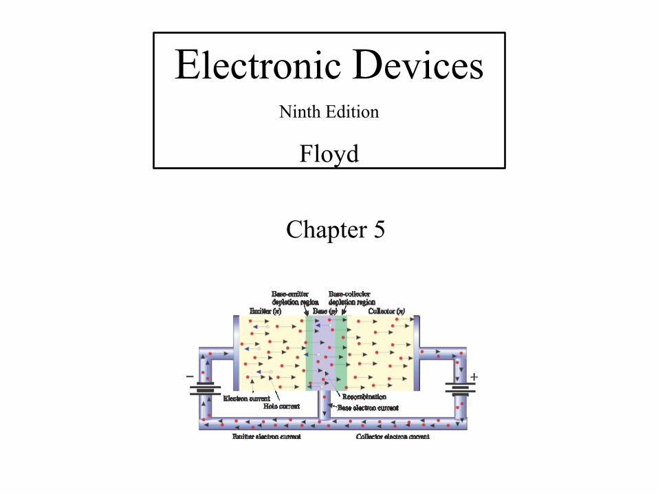
© 2012 Pearson Education. Upper Saddle River, NJ, 07458. All rights reserved. Electronic Devices, 9th edition Thomas L. Floyd Electronic Devices Ninth Edition Floyd Chapter 5
-
Upload
phungduong -
Category
Documents
-
view
351 -
download
15
Transcript of Electronic Devices -...
© 2012 Pearson Education. Upper Saddle River, NJ, 07458.
All rights reserved. Electronic Devices, 9th edition
Thomas L. Floyd
Electronic Devices Ninth Edition
Floyd
Chapter 5
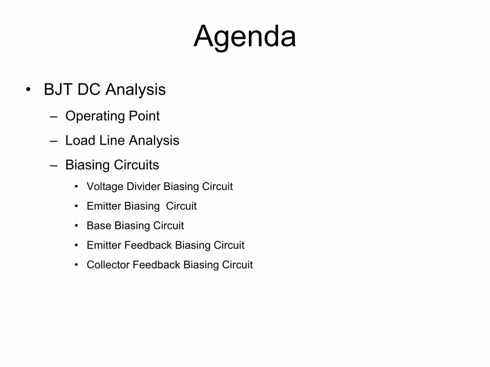
Agenda
• BJT DC Analysis
– Operating Point
– Load Line Analysis
– Biasing Circuits
• Voltage Divider Biasing Circuit
• Emitter Biasing Circuit
• Base Biasing Circuit
• Emitter Feedback Biasing Circuit
• Collector Feedback Biasing Circuit
© 2012 Pearson Education. Upper Saddle River, NJ, 07458.
All rights reserved. Electronic Devices, 9th edition
Thomas L. Floyd
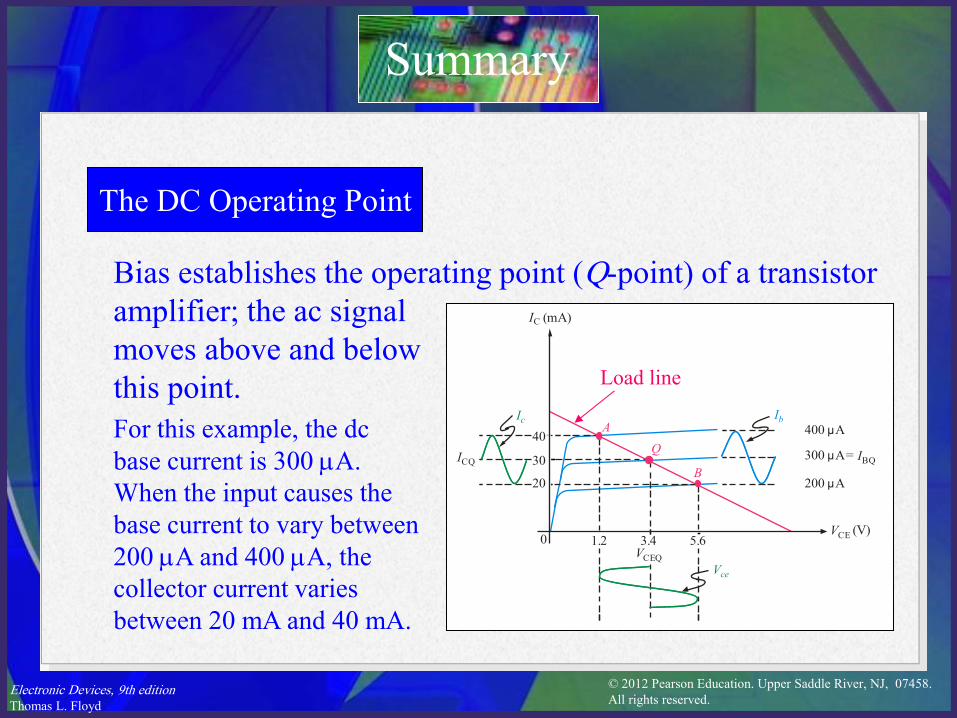
The DC Operating Point
Bias establishes the operating point (Q-point) of a transistor
amplifier; the ac signal
moves above and below
this point.
Summary
For this example, the dc
base current is 300 mA.
When the input causes the
base current to vary between
200 mA and 400 mA, the
collector current varies
between 20 mA and 40 mA.
0VCE (V)
400 A
IC (mA)
300 A = IBQ
200 A
A
B
Q
1.2 3.4 5.6VCEQ
ICQ
Vce
IbIc
20
30
40µ
µ
µ
Load line
© 2012 Pearson Education. Upper Saddle River, NJ, 07458.
All rights reserved. Electronic Devices, 9th edition
Thomas L. Floyd
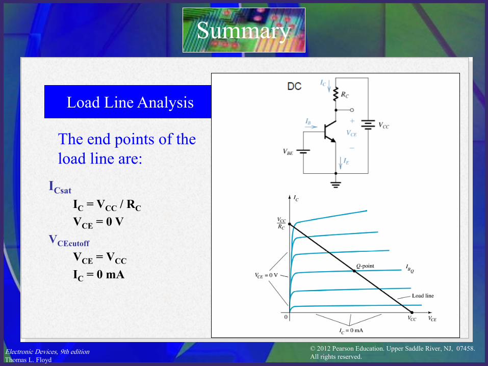
Load Line Analysis
The end points of the
load line are:
Summary
ICsat
IC = VCC / RC
VCE = 0 V
VCEcutoff
VCE = VCC
IC = 0 mA
© 2012 Pearson Education. Upper Saddle River, NJ, 07458.
All rights reserved. Electronic Devices, 9th edition
Thomas L. Floyd
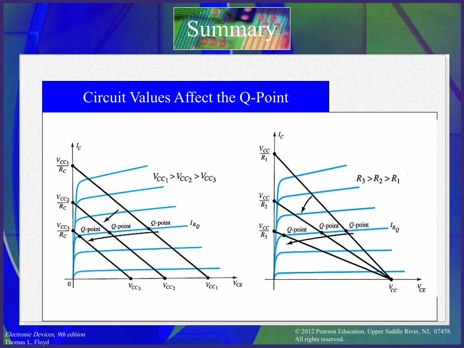
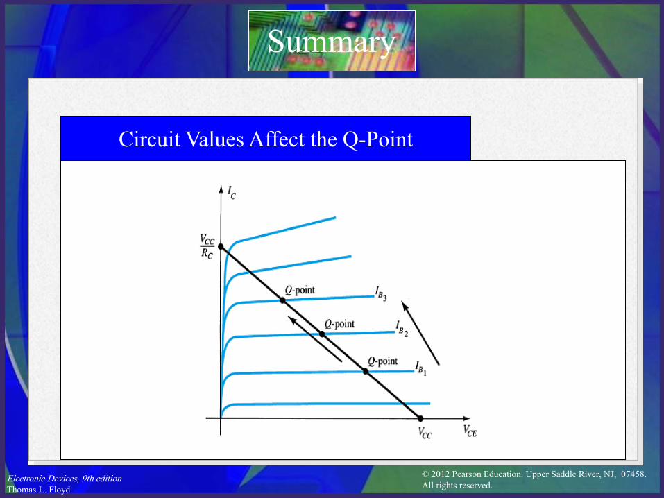
Summary
Circuit Values Affect the Q-Point
© 2012 Pearson Education. Upper Saddle River, NJ, 07458.
All rights reserved. Electronic Devices, 9th edition
Thomas L. Floyd
Circuit Values Affect the Q-Point
Summary
© 2012 Pearson Education. Upper Saddle River, NJ, 07458.
All rights reserved. Electronic Devices, 9th edition
Thomas L. Floyd
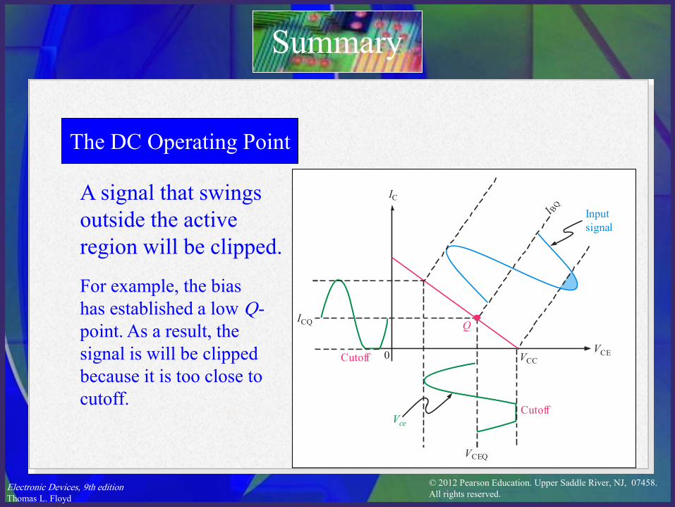
The DC Operating Point
A signal that swings
outside the active
region will be clipped.
Summary
For example, the bias
has established a low Q-
point. As a result, the
signal is will be clipped
because it is too close to
cutoff.
VCC
VCE
Cutoff
Q
I BQ
IC
ICQ
Cutoff 0
Vce
VCEQ
Input
signal
© 2012 Pearson Education. Upper Saddle River, NJ, 07458.
All rights reserved. Electronic Devices, 9th edition
Thomas L. Floyd
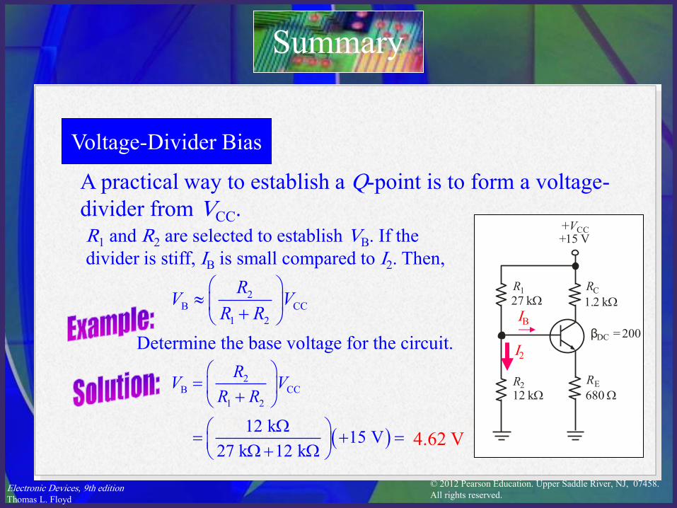
Voltage-Divider Bias
A practical way to establish a Q-point is to form a voltage-
divider from VCC.
Summary
R1 and R2 are selected to establish VB. If the
divider is stiff, IB is small compared to I2. Then,
+VCC
RCR1
RER2
2B CC
1 2
RV V
R R
+VCC
RCR1
RER2
βDC = 200
27 kW
12 kW
+15 V
680 W
1.2 kW
Determine the base voltage for the circuit.
2B CC
1 2
12 k15 V
27 k 12 k
RV V
R R
W
W W 4.62 V
I2
IB
© 2012 Pearson Education. Upper Saddle River, NJ, 07458.
All rights reserved. Electronic Devices, 9th edition
Thomas L. Floyd
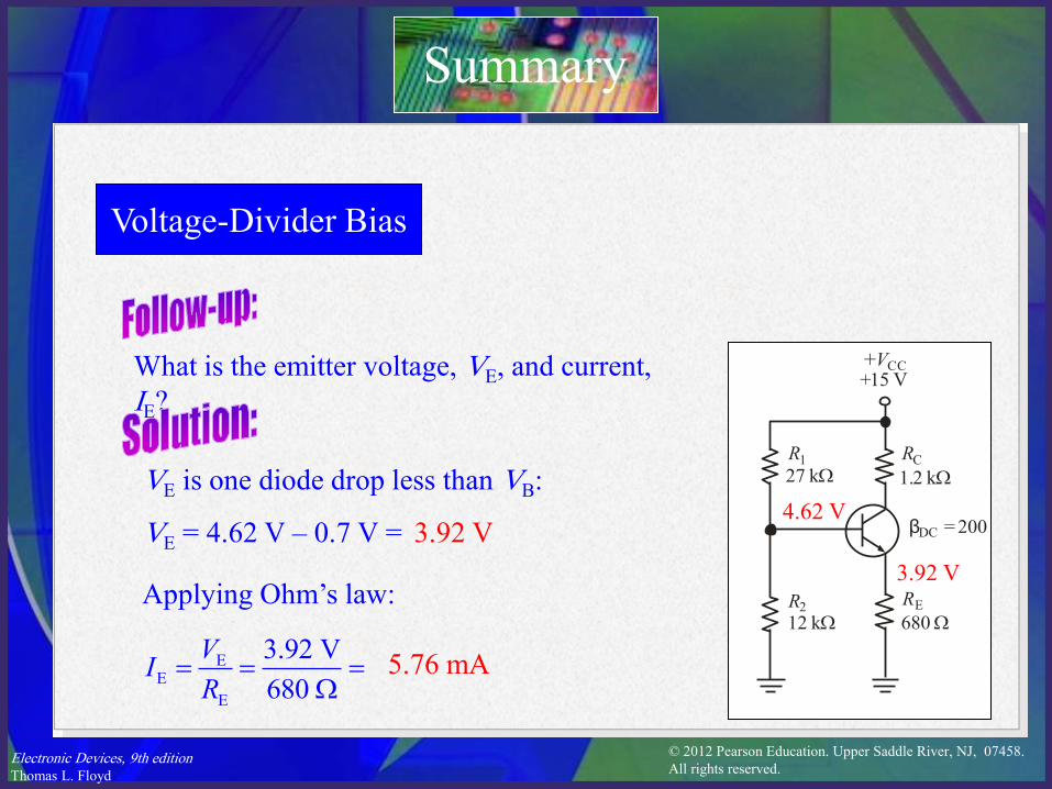
Voltage-Divider Bias
Summary
+VCC
RCR1
RER2
βDC = 200
27 kW
12 kW
+15 V
680 W
1.2 kW
4.62 V
What is the emitter voltage, VE, and current,
IE?
VE is one diode drop less than VB:
VE = 4.62 V – 0.7 V = 3.92 V
3.92 V Applying Ohm’s law:
EE
E
3.92 V
680
VI
R
W5.76 mA
© 2012 Pearson Education. Upper Saddle River, NJ, 07458.
All rights reserved. Electronic Devices, 9th edition
Thomas L. Floyd
Summary
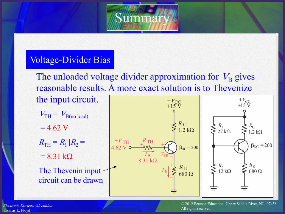
Voltage-Divider Bias
The unloaded voltage divider approximation for VB gives
reasonable results. A more exact solution is to Thevenize
the input circuit. +VCC
RCR1
RER2
βDC = 200
27 kW
12 kW
+15 V
680 W
1.2 kW
VTH = VB(no load)
= 4.62 V
RTH = R1||R2 =
= 8.31 kW
The Thevenin input
circuit can be drawn
R C
R TH
+VCC
R E
+V TH+ –
IB
+
+
–
–
IE
VBE
8.31 kW
680 W
1.2 kW
4.62 V
+15 V
βDC = 200
© 2012 Pearson Education. Upper Saddle River, NJ, 07458.
All rights reserved. Electronic Devices, 9th edition
Thomas L. Floyd
Summary
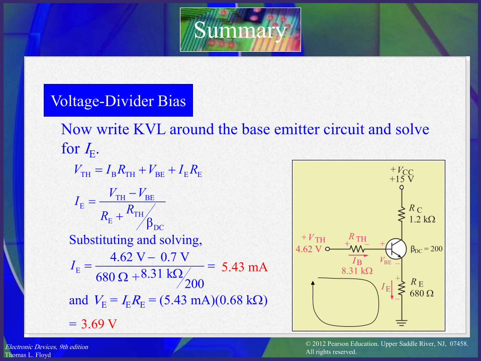
Voltage-Divider Bias
Now write KVL around the base emitter circuit and solve
for IE.
R C
R TH
+VCC
R E
+V TH+ –
IB
+
+
–
–
IE
VBE
8.31 kW
680 W
1.2 kW
4.62 V
+15 V
βDC = 200
TH B TH BE E EV I R V I R
TH BEE
THE
DCβ
V VI
RR
Substituting and solving,
E
4.62 V 0.7 V
8.31 k680 +200
I
WW
5.43 mA
and VE = IERE = (5.43 mA)(0.68 kW
= 3.69 V
© 2012 Pearson Education. Upper Saddle River, NJ, 07458.
All rights reserved. Electronic Devices, 9th edition
Thomas L. Floyd
Summary
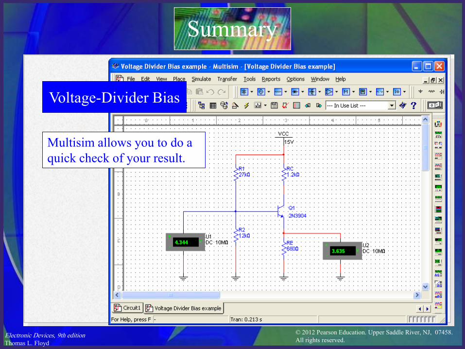
Voltage-Divider Bias
Multisim allows you to do a
quick check of your result.
© 2012 Pearson Education. Upper Saddle River, NJ, 07458.
All rights reserved. Electronic Devices, 9th edition
Thomas L. Floyd
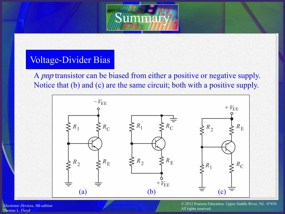
Summary
Voltage-Divider Bias
A pnp transistor can be biased from either a positive or negative supply.
Notice that (b) and (c) are the same circuit; both with a positive supply.
+
+
V V
V
EE
EE
EE
R
RR
2
221
11
R
RR
R
RR
C
CCR
RR
E
EE
(a) (b) (c)
© 2012 Pearson Education. Upper Saddle River, NJ, 07458.
All rights reserved. Electronic Devices, 9th edition
Thomas L. Floyd
Summary
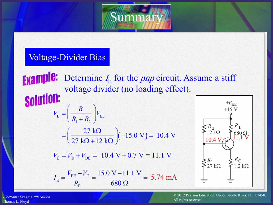
Voltage-Divider Bias
Determine IE for the pnp circuit. Assume a stiff
voltage divider (no loading effect).
+VEE
R2
1R RC
1.2 kW
R E
680 W
27 kW
12 kW
+15 V
1B EE
1 2
27 k15.0 V 10.4 V
27 k 12 k
RV V
R R
W
W W
E B BE 10.4 V 0.7 V = 11.1 VV V V
EE EE
E
15.0 V 11.1 V
680
V VI
R
W5.74 mA
10.4 V 11.1 V
© 2012 Pearson Education. Upper Saddle River, NJ, 07458.
All rights reserved. Electronic Devices, 9th edition
Thomas L. Floyd
Summary
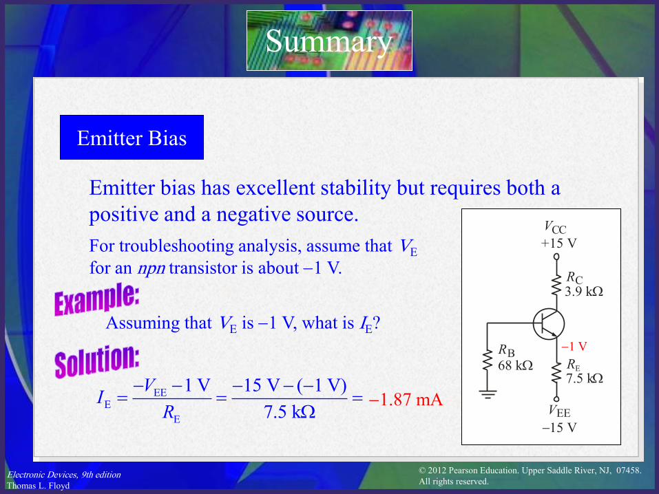
Emitter Bias
Emitter bias has excellent stability but requires both a
positive and a negative source.
Assuming that VE is 1 V, what is IE?
V
V
CC
EE
RC
RE
RB68 kW
+15 V
15 V
7.5 kW
3.9 kW
For troubleshooting analysis, assume that VE
for an npn transistor is about 1 V.
1 V
EEE
E
1 V 15 V ( 1 V)
7.5 k
VI
R
W1.87 mA
© 2012 Pearson Education. Upper Saddle River, NJ, 07458.
All rights reserved. Electronic Devices, 9th edition
Thomas L. Floyd
Summary
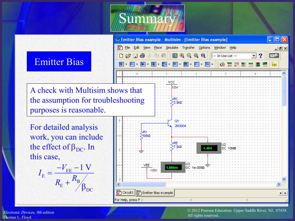
Emitter Bias
A check with Multisim shows that
the assumption for troubleshooting
purposes is reasonable.
For detailed analysis
work, you can include
the effect of bDC. In
this case,
EEE
BE
DC
1 V
β
VI
RR

© 2012 Pearson Education. Upper Saddle River, NJ, 07458.
All rights reserved. Electronic Devices, 9th edition
Thomas L. Floyd
Summary
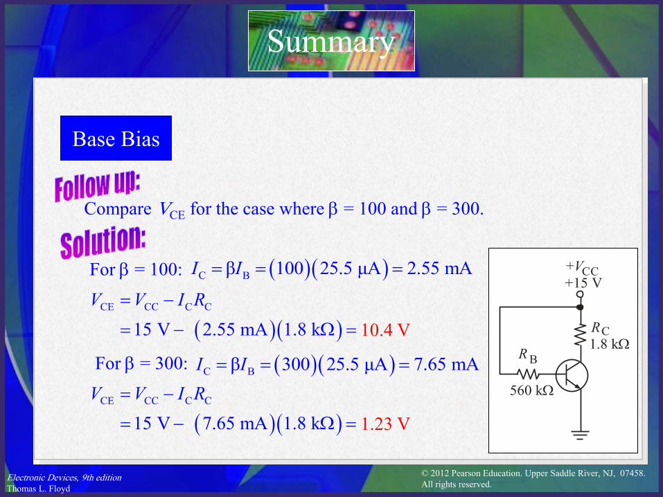
Base Bias
RC
R B
+VCC
Base bias is used in switching circuits because of its
simplicity, but not widely used in linear applications
because the Q-point is b dependent.
Base current is derived from the collector supply
through a large base resistor.
What is IB?
CCB
B
0.7 V 15 V 0.7 V
560 k
VI
R
W25.5 mA
RC
R B
+VCC
560 kW
+15 V
1.8 kW
© 2012 Pearson Education. Upper Saddle River, NJ, 07458.
All rights reserved. Electronic Devices, 9th edition
Thomas L. Floyd
Summary
Base Bias
Compare VCE for the case where b = 100 and b = 300.
RC
R B
+VCC
560 kW
+15 V
1.8 kW
C Bβ 100 25.5 μA 2.55 mAI I
10.4 V
For b = 100:
CE CC C C
15 V 2.55 mA 1.8 k
V V I R
W
For b = 300: C Bβ 300 25.5 μA 7.65 mAI I
CE CC C C
15 V 7.65 mA 1.8 k
V V I R
W 1.23 V
© 2012 Pearson Education. Upper Saddle River, NJ, 07458.
All rights reserved. Electronic Devices, 9th edition
Thomas L. Floyd
Summary
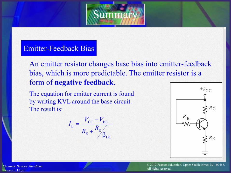
Emitter-Feedback Bias
R
R
C
E
R B
+VCC
An emitter resistor changes base bias into emitter-feedback
bias, which is more predictable. The emitter resistor is a
form of negative feedback.
The equation for emitter current is found
by writing KVL around the base circuit.
The result is:
CC BEE
EE
DCβ
V VI
RR
© 2012 Pearson Education. Upper Saddle River, NJ, 07458.
All rights reserved. Electronic Devices, 9th edition
Thomas L. Floyd
Summary
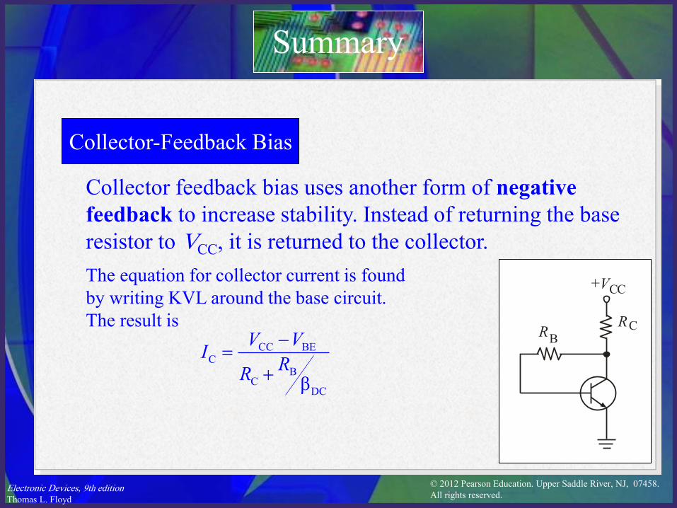
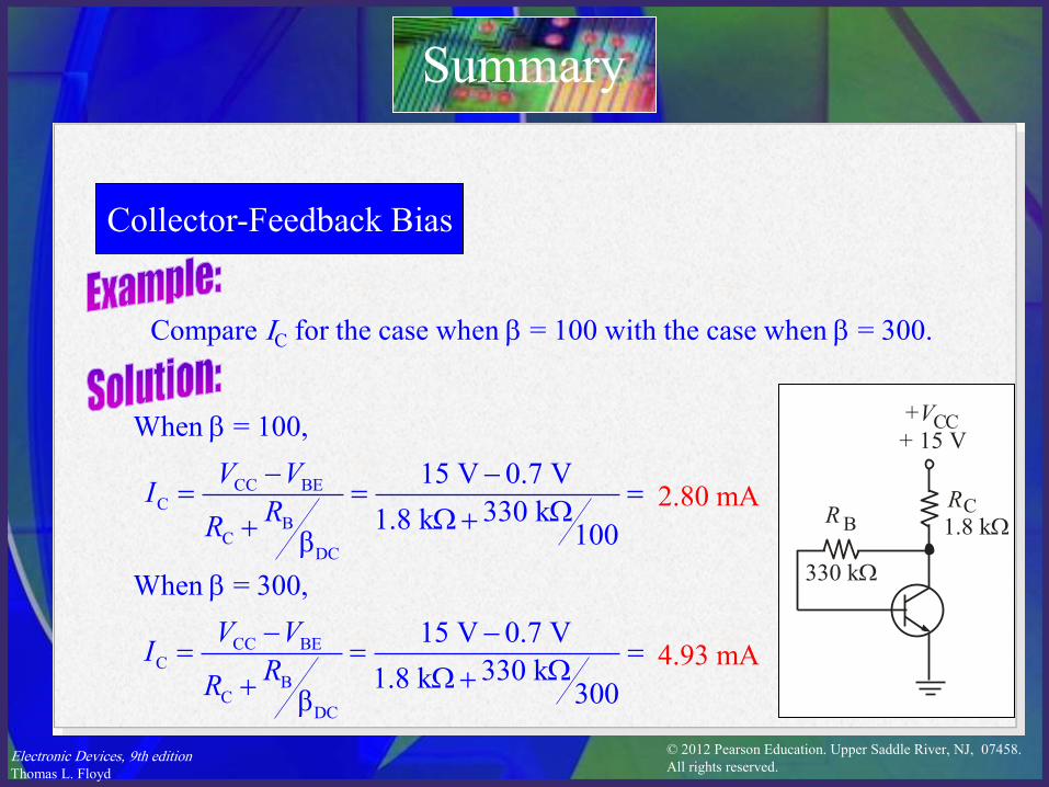
Collector-Feedback Bias
Collector feedback bias uses another form of negative
feedback to increase stability. Instead of returning the base
resistor to VCC, it is returned to the collector.
The equation for collector current is found
by writing KVL around the base circuit.
The result is
CC BEC
BC
DCβ
V VI
RR
+VCC
RCRB
© 2012 Pearson Education. Upper Saddle River, NJ, 07458.
All rights reserved. Electronic Devices, 9th edition
Thomas L. Floyd
Summary
Collector-Feedback Bias
When b = 100,
CC BEC
BC
DC
15 V 0.7 V
330 k1.8 k100β
V VI
RR
WW
+VCC
RCR B
330 kW
1.8 kW
+ 15 V
Compare IC for the case when b = 100 with the case when b = 300.
2.80 mA
When b = 300,
CC BEC
BC
DC
15 V 0.7 V
330 k1.8 k300β
V VI
RR
WW 4.93 mA
© 2012 Pearson Education. Upper Saddle River, NJ, 07458.
All rights reserved. Electronic Devices, 9th edition
Thomas L. Floyd
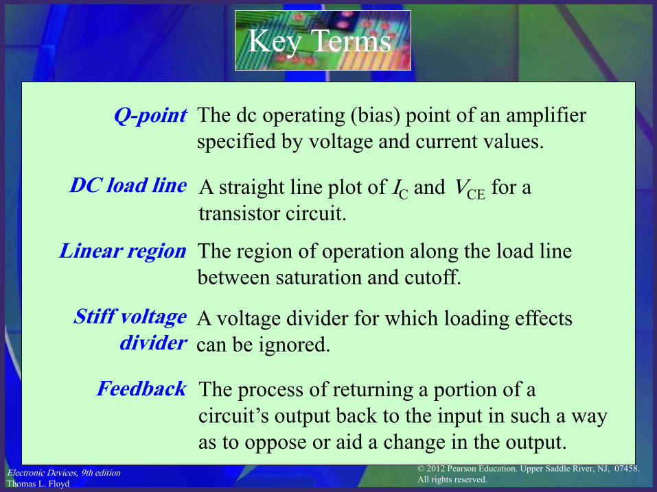
Key Terms
Q-point
DC load line
Linear region
Stiff voltage
divider
Feedback
The dc operating (bias) point of an amplifier
specified by voltage and current values.
A straight line plot of IC and VCE for a
transistor circuit.
The region of operation along the load line
between saturation and cutoff.
A voltage divider for which loading effects
can be ignored.
The process of returning a portion of a
circuit’s output back to the input in such a way
as to oppose or aid a change in the output.
© 2012 Pearson Education. Upper Saddle River, NJ, 07458.
All rights reserved. Electronic Devices, 9th edition
Thomas L. Floyd
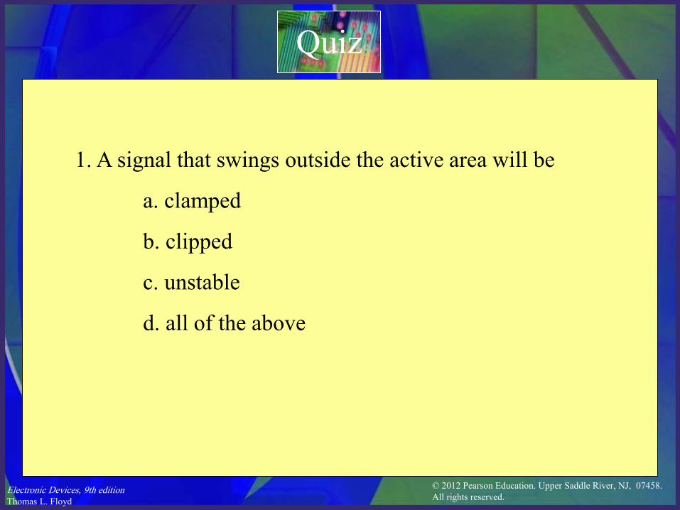
Quiz
1. A signal that swings outside the active area will be
a. clamped
b. clipped
c. unstable
d. all of the above

© 2012 Pearson Education. Upper Saddle River, NJ, 07458.
All rights reserved. Electronic Devices, 9th edition
Thomas L. Floyd
Quiz
2. A stiff voltage divider is one in which
a. there is no load current
b. divider current is small compared to load current
c. the load is connected directly to the source voltage
d. loading effects can be ignored
© 2012 Pearson Education. Upper Saddle River, NJ, 07458.
All rights reserved. Electronic Devices, 9th edition
Thomas L. Floyd
Quiz
3. Assuming a stiff voltage-divider for the circuit shown,
the emitter voltage is
a. 4.3 V
b. 5.7 V
c. 6.8 V
d. 9.3 V
+VCC
RCR1
RER2
βDC = 200
20 kW
10 kW
+15 V
1.2 kW
1.8 kW
© 2012 Pearson Education. Upper Saddle River, NJ, 07458.
All rights reserved. Electronic Devices, 9th edition
Thomas L. Floyd
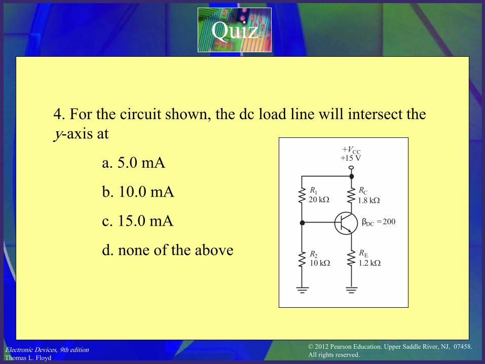
Quiz
4. For the circuit shown, the dc load line will intersect the
y-axis at
a. 5.0 mA
b. 10.0 mA
c. 15.0 mA
d. none of the above
+VCC
RCR1
RER2
βDC = 200
20 kW
10 kW
+15 V
1.2 kW
1.8 kW
© 2012 Pearson Education. Upper Saddle River, NJ, 07458.
All rights reserved. Electronic Devices, 9th edition
Thomas L. Floyd
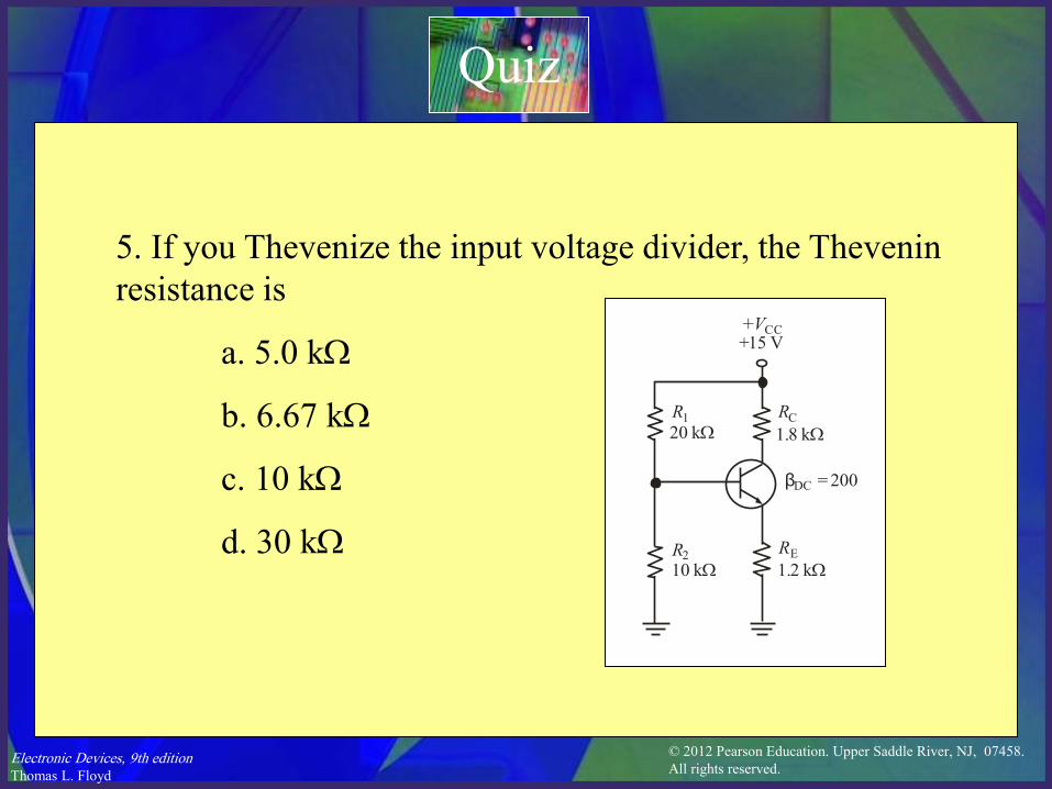
Quiz
5. If you Thevenize the input voltage divider, the Thevenin
resistance is
a. 5.0 kW
b. 6.67 kW
c. 10 kW
d. 30 kW
+VCC
RCR1
RER2
βDC = 200
20 kW
10 kW
+15 V
1.2 kW
1.8 kW
© 2012 Pearson Education. Upper Saddle River, NJ, 07458.
All rights reserved. Electronic Devices, 9th edition
Thomas L. Floyd
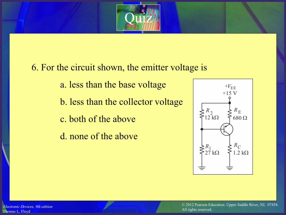
Quiz
6. For the circuit shown, the emitter voltage is
a. less than the base voltage
b. less than the collector voltage
c. both of the above
d. none of the above
+VEE
R2
1R RC
1.2 kW
R E
680 W
27 kW
12 kW
+15 V
© 2012 Pearson Education. Upper Saddle River, NJ, 07458.
All rights reserved. Electronic Devices, 9th edition
Thomas L. Floyd
Quiz
7. Emitter bias
a. is not good for linear circuits
b. uses a voltage-divider on the input
c. requires dual power supplies
d. all of the above
© 2012 Pearson Education. Upper Saddle River, NJ, 07458.
All rights reserved. Electronic Devices, 9th edition
Thomas L. Floyd
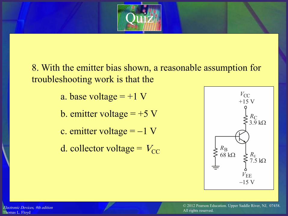
Quiz
8. With the emitter bias shown, a reasonable assumption for
troubleshooting work is that the
a. base voltage = +1 V
b. emitter voltage = +5 V
c. emitter voltage = 1 V
d. collector voltage = VCC
V
V
CC
EE
RC
RE
RB68 kW
+15 V
15 V
7.5 kW
3.9 kW
© 2012 Pearson Education. Upper Saddle River, NJ, 07458.
All rights reserved. Electronic Devices, 9th edition
Thomas L. Floyd
Quiz
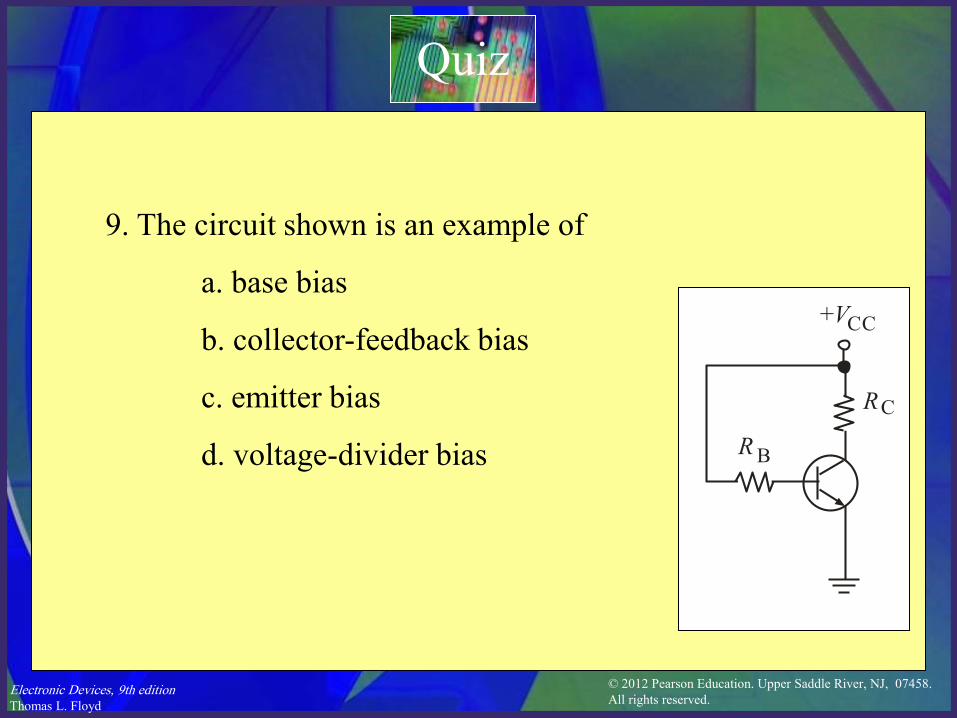
9. The circuit shown is an example of
a. base bias
b. collector-feedback bias
c. emitter bias
d. voltage-divider bias
RC
R B
+VCC
© 2012 Pearson Education. Upper Saddle River, NJ, 07458.
All rights reserved. Electronic Devices, 9th edition
Thomas L. Floyd
Quiz
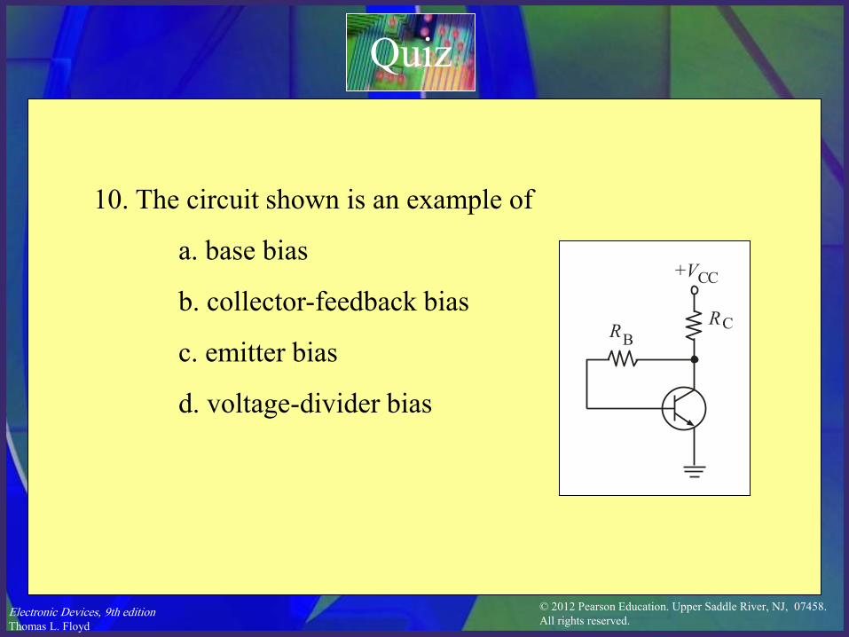
10. The circuit shown is an example of
a. base bias
b. collector-feedback bias
c. emitter bias
d. voltage-divider bias
+VCC
RCRB
© 2012 Pearson Education. Upper Saddle River, NJ, 07458.
All rights reserved. Electronic Devices, 9th edition
Thomas L. Floyd
Quiz
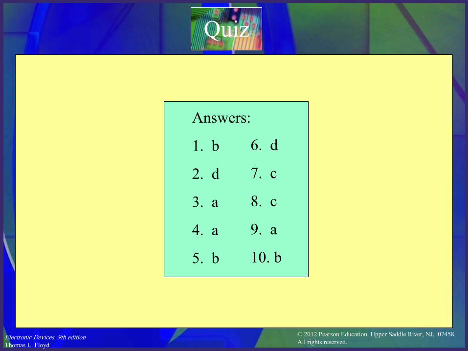
Answers:
1. b
2. d
3. a
4. a
5. b
6. d
7. c
8. c
9. a
10. b
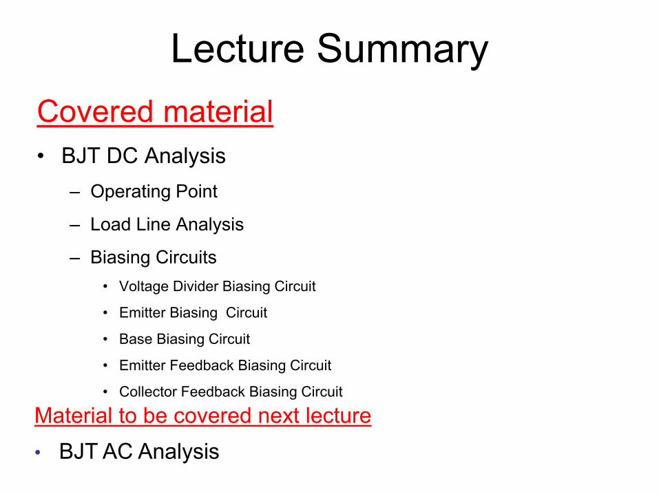
Lecture Summary
Covered material
• BJT DC Analysis
– Operating Point
– Load Line Analysis
– Biasing Circuits
• Voltage Divider Biasing Circuit
• Emitter Biasing Circuit
• Base Biasing Circuit
• Emitter Feedback Biasing Circuit
• Collector Feedback Biasing Circuit
Material to be covered next lecture
• BJT AC Analysis