Electronic Devices - ECED Mansoura « Academic Site€¦ · · 2014-12-16Electronic Devices, th...
50
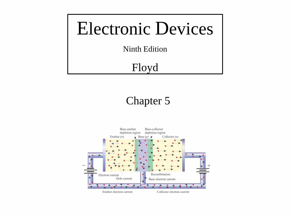
Electronic Devices Ninth Edition Floyd Chapter 5
Transcript of Electronic Devices - ECED Mansoura « Academic Site€¦ · · 2014-12-16Electronic Devices, th...
© 2012 Pearson Education. Upper Saddle River, NJ, 07458. All rights reserved.
Electronic Devices, 9th edition Thomas L. Floyd
Electronic Devices Ninth Edition
Floyd
Chapter 5
© 2012 Pearson Education. Upper Saddle River, NJ, 07458. All rights reserved.
Electronic Devices, 9th edition Thomas L. Floyd
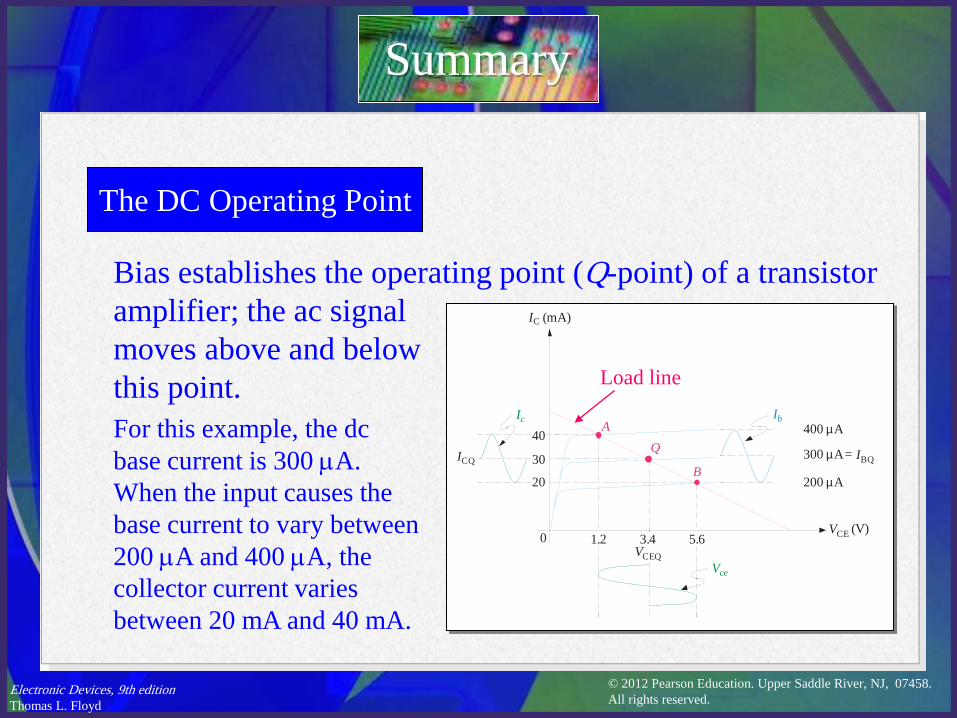
The DC Operating Point
Bias establishes the operating point (Q-point) of a transistor amplifier; the ac signal moves above and below this point.
Summary
For this example, the dc base current is 300 µA. When the input causes the base current to vary between 200 µA and 400 µA, the collector current varies between 20 mA and 40 mA.
0VCE (V)
400 A
IC (mA)
300 A = IBQ
200 A
A
B
Q
1.2 3.4 5.6VCEQ
ICQ
Vce
IbIc
20
30
40 µ
µ
µ
Load line
© 2012 Pearson Education. Upper Saddle River, NJ, 07458. All rights reserved.
Electronic Devices, 9th edition Thomas L. Floyd
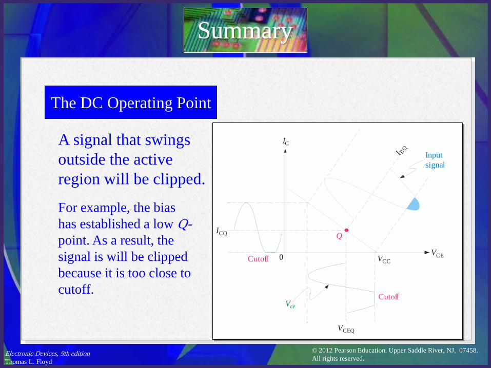
The DC Operating Point
A signal that swings outside the active region will be clipped.
Summary
For example, the bias has established a low Q- point. As a result, the signal is will be clipped because it is too close to cutoff.
VCCVCE
Cutoff
Q
I BQ
IC
ICQ
Cutoff 0
Vce
VCEQ
Inputsignal
© 2012 Pearson Education. Upper Saddle River, NJ, 07458. All rights reserved.
Electronic Devices, 9th edition Thomas L. Floyd
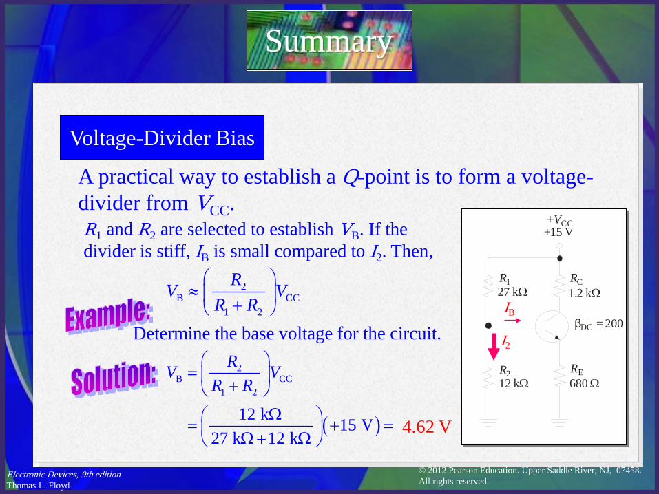
Voltage-Divider Bias
A practical way to establish a Q-point is to form a voltage-divider from VCC.
Summary
R1 and R2 are selected to establish VB. If the divider is stiff, IB is small compared to I2. Then,
+VCC
RCR1
RER2
2B CC
1 2
RV VR R
≈ +
+VCC
RCR1
RER2
βDC = 200
27 kΩ
12 kΩ
+15 V
680 Ω
1.2 kΩ
Determine the base voltage for the circuit.
( )
2B CC
1 2
12 k 15 V27 k 12 k
RV VR R
= +
Ω = + = Ω + Ω 4.62 V
I2
IB
© 2012 Pearson Education. Upper Saddle River, NJ, 07458. All rights reserved.
Electronic Devices, 9th edition Thomas L. Floyd
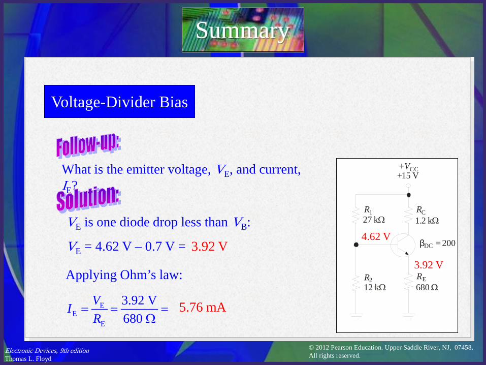
Voltage-Divider Bias
Summary
+VCC
RCR1
RER2
βDC = 200
27 kΩ
12 kΩ
+15 V
680 Ω
1.2 kΩ
4.62 V
What is the emitter voltage, VE, and current, IE?
VE is one diode drop less than VB:
VE = 4.62 V – 0.7 V = 3.92 V 3.92 V
Applying Ohm’s law:
EE
E
3.92 V680
VIR
= = =Ω
5.76 mA
© 2012 Pearson Education. Upper Saddle River, NJ, 07458. All rights reserved.
Electronic Devices, 9th edition Thomas L. Floyd
Summary
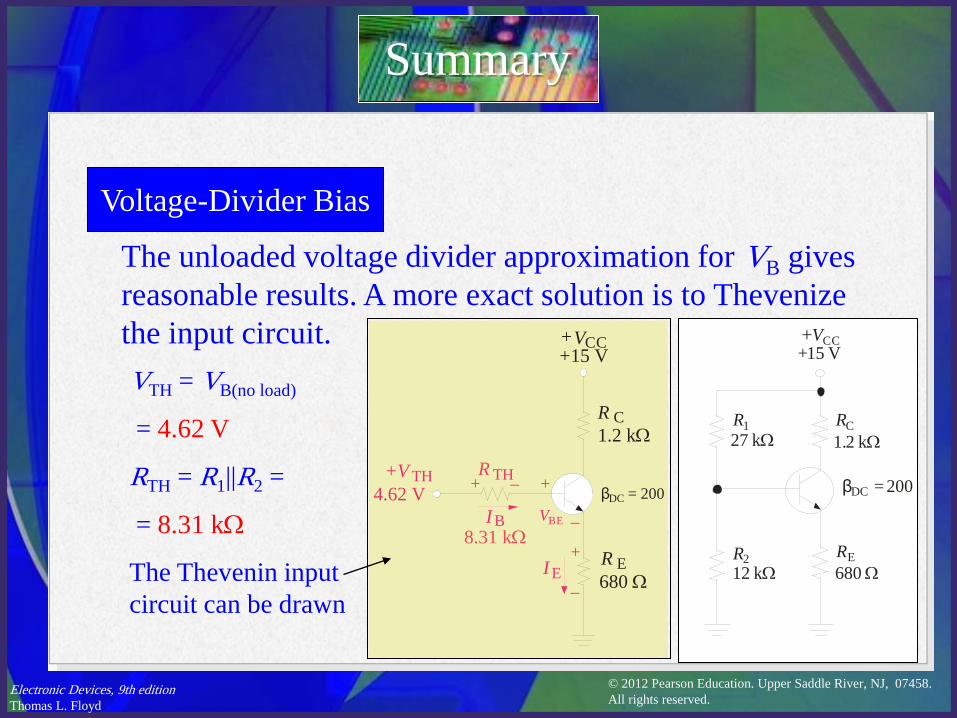
Voltage-Divider Bias
The unloaded voltage divider approximation for VB gives reasonable results. A more exact solution is to Thevenize the input circuit. +VCC
RCR1
RER2
βDC = 200
27 kΩ
12 kΩ
+15 V
680 Ω
1.2 kΩ
VTH = VB(no load)
= 4.62 V
RTH = R1||R2 = = 8.31 kΩ
The Thevenin input circuit can be drawn
R C
R TH
+VCC
R E
+V TH + –
IB
+
+
–
–I E
VBE
8.31 kΩ
680 Ω
1.2 kΩ
4.62 V
+15 V
βDC = 200
© 2012 Pearson Education. Upper Saddle River, NJ, 07458. All rights reserved.
Electronic Devices, 9th edition Thomas L. Floyd
Summary
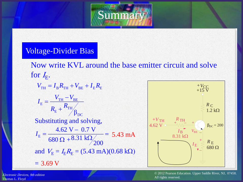
Voltage-Divider Bias
Now write KVL around the base emitter circuit and solve for IE.
R C
R TH
+VCC
R E
+V TH + –
IB
+
+
–
–I E
VBE
8.31 kΩ
680 Ω
1.2 kΩ
4.62 V
+15 V
βDC = 200
TH B TH BE E EV I R V I R= + +
TH BEE
THE
DCβ
V VI RR
−=
+
Substituting and solving,
E4.62 V 0.7 V
8.31 k680 + 200I −
= =ΩΩ
5.43 mA
and VE = IERE = (5.43 mA)(0.68 kΩ)
= 3.69 V
© 2012 Pearson Education. Upper Saddle River, NJ, 07458. All rights reserved.
Electronic Devices, 9th edition Thomas L. Floyd
Summary
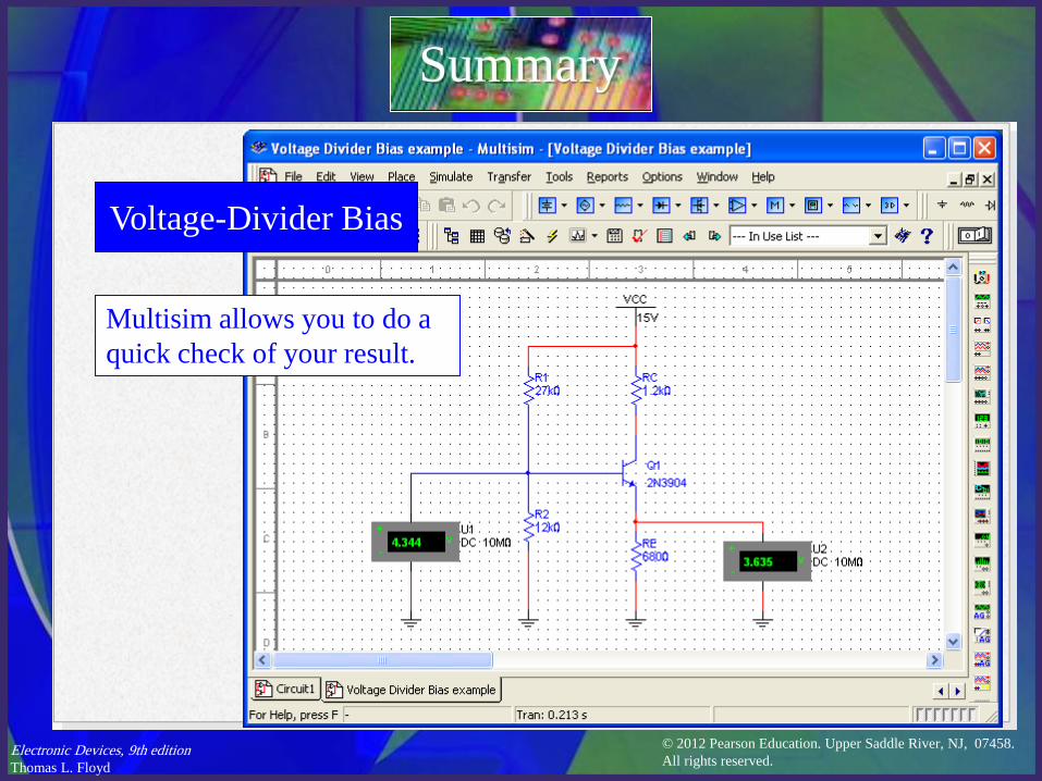
Voltage-Divider Bias
Multisim allows you to do a quick check of your result.
© 2012 Pearson Education. Upper Saddle River, NJ, 07458. All rights reserved.
Electronic Devices, 9th edition Thomas L. Floyd
Summary
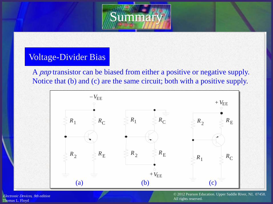
Voltage-Divider Bias A pnp transistor can be biased from either a positive or negative supply. Notice that (b) and (c) are the same circuit; both with a positive supply.
+
+
V V
V
EEEE
EE
R
RR
2
22 1
11
R
RR
R
RR
C
CC R
RR
E
EE
−
(a) (b) (c)
© 2012 Pearson Education. Upper Saddle River, NJ, 07458. All rights reserved.
Electronic Devices, 9th edition Thomas L. Floyd
Summary
Voltage-Divider Bias
Determine IE for the pnp circuit. Assume a stiff voltage divider (no loading effect).
+VEE
R 2
1R RC1.2 kΩ
R E680 Ω
27 kΩ
12 kΩ
+15 V
( )
1B EE
1 2
27 k 15.0 V 10.4 V27 k 12 k
RV VR R
= +
Ω = + = Ω + Ω
E B BE 10.4 V 0.7 V = 11.1 VV V V= + = +
EE EE
E
15.0 V 11.1 V680
V VIR
− −= = =
Ω5.74 mA
10.4 V 11.1 V
© 2012 Pearson Education. Upper Saddle River, NJ, 07458. All rights reserved.
Electronic Devices, 9th edition Thomas L. Floyd
Summary
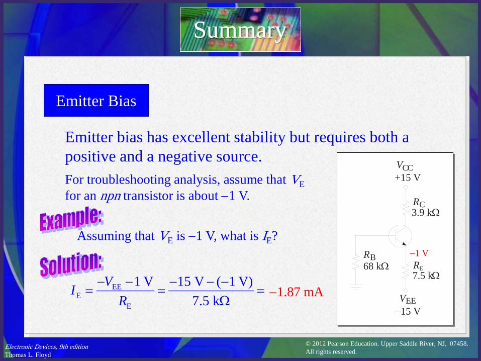
Emitter Bias
Emitter bias has excellent stability but requires both a positive and a negative source.
Assuming that VE is −1 V, what is IE?
V
V
CC
EE
RC
RE
RB68 kΩ
+15 V
−15 V
7.5 kΩ
3.9 kΩ
For troubleshooting analysis, assume that VE for an npn transistor is about −1 V.
−1 V
EEE
E
1 V 15 V ( 1 V)7.5 k
VIR
− − − − −= = =
Ω−1.87 mA
© 2012 Pearson Education. Upper Saddle River, NJ, 07458. All rights reserved.
Electronic Devices, 9th edition Thomas L. Floyd
Summary
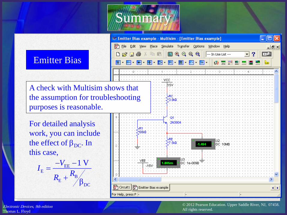
Emitter Bias
A check with Multisim shows that the assumption for troubleshooting purposes is reasonable.
For detailed analysis work, you can include the effect of βDC. In this case,
EEE
BE
DC
1 V
β
VI RR
− −=
+
© 2012 Pearson Education. Upper Saddle River, NJ, 07458. All rights reserved.
Electronic Devices, 9th edition Thomas L. Floyd
Summary
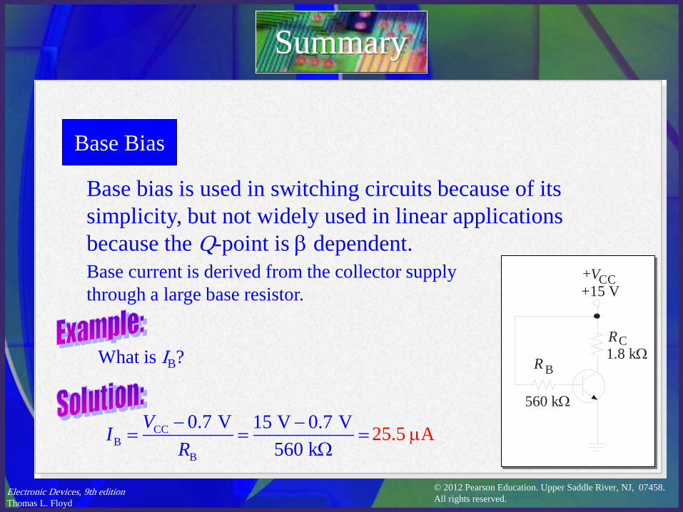
Base Bias
RC
R B
+VCC
Base bias is used in switching circuits because of its simplicity, but not widely used in linear applications because the Q-point is β dependent. Base current is derived from the collector supply through a large base resistor.
What is IB?
CCB
B
0.7 V 15 V 0.7 V560 k
VIR− −
= = =Ω
25.5 µA
RC
R B
+VCC
560 kΩ
+15 V
1.8 kΩ
© 2012 Pearson Education. Upper Saddle River, NJ, 07458. All rights reserved.
Electronic Devices, 9th edition Thomas L. Floyd
Summary
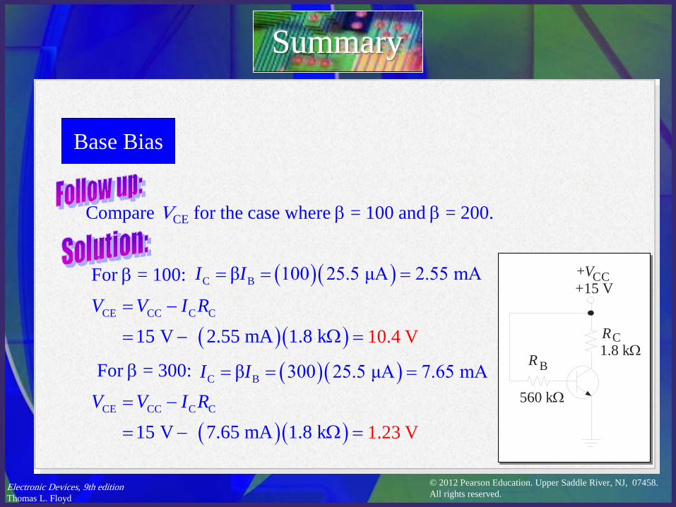
Base Bias
Compare VCE for the case where β = 100 and β = 200.
RC
R B
+VCC
560 kΩ
+15 V
1.8 kΩ
( )( )C Bβ 100 25.5 μA 2.55 mAI I= = =
10.4 V
For β = 100:
( )( )CE CC C C
15 V 2.55 mA 1.8 kV V I R= −
= − Ω =
For β = 300: ( )( )C Bβ 300 25.5 μA 7.65 mAI I= = =
( )( )CE CC C C
15 V 7.65 mA 1.8 kV V I R= −
= − Ω = 1.23 V
© 2012 Pearson Education. Upper Saddle River, NJ, 07458. All rights reserved.
Electronic Devices, 9th edition Thomas L. Floyd
Summary
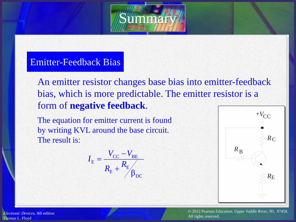
Emitter-Feedback Bias
R
R
C
E
R B
+VCC
An emitter resistor changes base bias into emitter-feedback bias, which is more predictable. The emitter resistor is a form of negative feedback. The equation for emitter current is found by writing KVL around the base circuit. The result is:
CC BEE
EE
DCβ
V VI RR
−=
+
© 2012 Pearson Education. Upper Saddle River, NJ, 07458. All rights reserved.
Electronic Devices, 9th edition Thomas L. Floyd
Summary
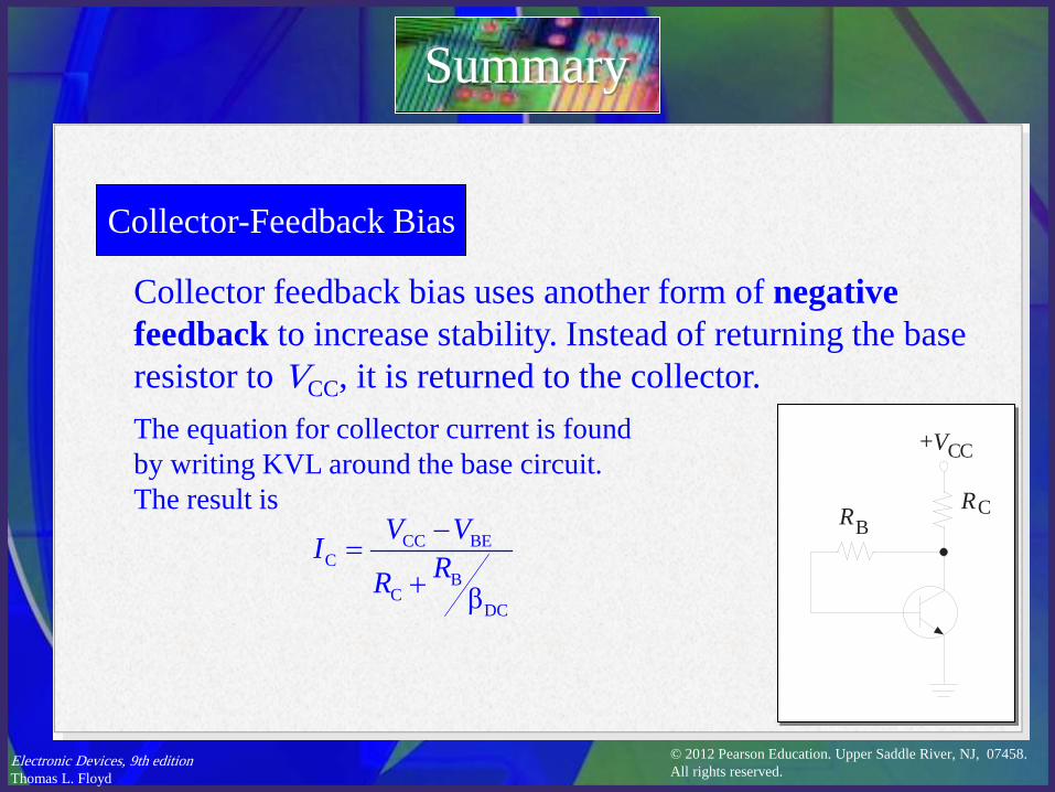
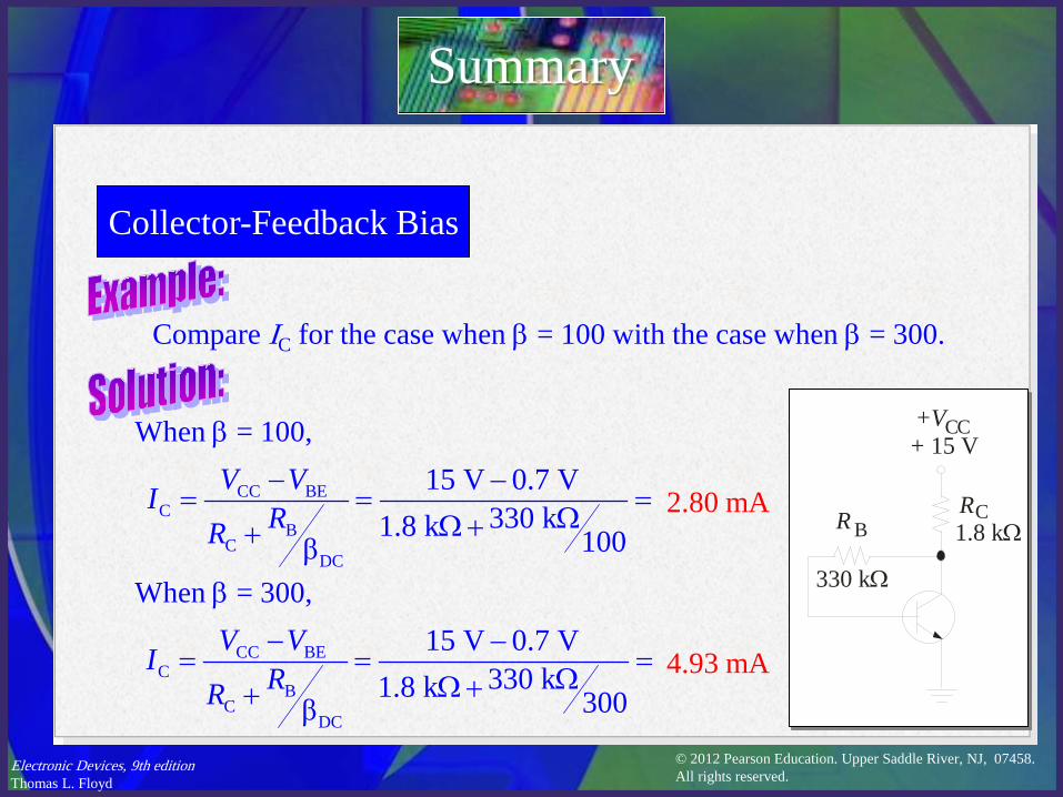
Collector-Feedback Bias
Collector feedback bias uses another form of negative feedback to increase stability. Instead of returning the base resistor to VCC, it is returned to the collector. The equation for collector current is found by writing KVL around the base circuit. The result is
CC BEC
BC
DCβ
V VI RR
−=
+
+VCC
RCRB
© 2012 Pearson Education. Upper Saddle River, NJ, 07458. All rights reserved.
Electronic Devices, 9th edition Thomas L. Floyd
Summary
Collector-Feedback Bias
When β = 100,
CC BEC
BC
DC
15 V 0.7 V330 k1.8 k 100β
V VI RR
− −= = =
ΩΩ ++
+VCC
RCR B
330 kΩ
1.8 kΩ
+ 15 V
Compare IC for the case when β = 100 with the case when β = 300.
2.80 mA
When β = 300,
CC BEC
BC
DC
15 V 0.7 V330 k1.8 k 300β
V VI RR
− −= = =
ΩΩ ++4.93 mA
© 2012 Pearson Education. Upper Saddle River, NJ, 07458. All rights reserved.
Electronic Devices, 9th edition Thomas L. Floyd
Electronic Devices Ninth Edition
Floyd
Chapter 6
© 2012 Pearson Education. Upper Saddle River, NJ, 07458. All rights reserved.
Electronic Devices, 9th edition Thomas L. Floyd
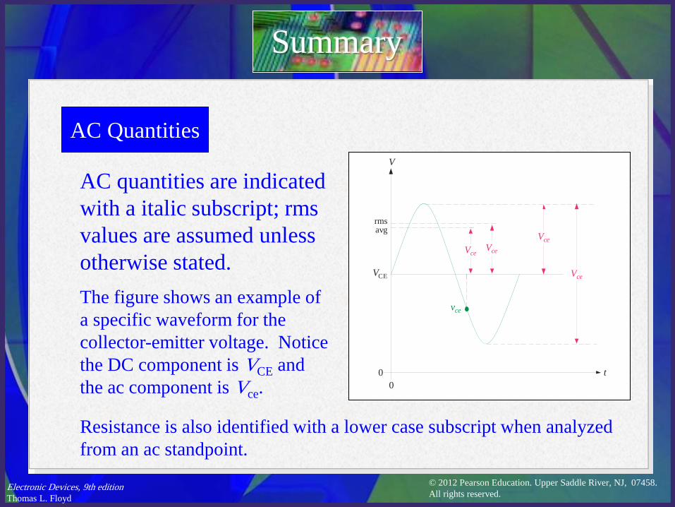
AC Quantities
AC quantities are indicated with a italic subscript; rms values are assumed unless otherwise stated.
Summary
VceVce
Vce
vce
VCE
00
t
Vce
rmsavg
V
The figure shows an example of a specific waveform for the collector-emitter voltage. Notice the DC component is VCE and the ac component is Vce.
Resistance is also identified with a lower case subscript when analyzed from an ac standpoint.
© 2012 Pearson Education. Upper Saddle River, NJ, 07458. All rights reserved.
Electronic Devices, 9th edition Thomas L. Floyd
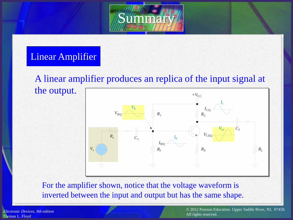
Linear Amplifier
A linear amplifier produces an replica of the input signal at the output.
Summary
For the amplifier shown, notice that the voltage waveform is inverted between the input and output but has the same shape.
RC
+VCC
R1
RER2 RL
C2
Vb
IbRs
Ic
ICQ
Vce
VCEQ
Vs
C1IBQ
VBQ
© 2012 Pearson Education. Upper Saddle River, NJ, 07458. All rights reserved.
Electronic Devices, 9th edition Thomas L. Floyd
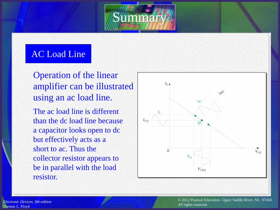
AC Load Line
Operation of the linear amplifier can be illustrated using an ac load line.
Summary
The ac load line is different than the dc load line because a capacitor looks open to dc but effectively acts as a short to ac. Thus the collector resistor appears to be in parallel with the load resistor.
VCEQ
0 VCE
I b
IC
Ic
Q
Vce
ICQ
I BQ
© 2012 Pearson Education. Upper Saddle River, NJ, 07458. All rights reserved.
Electronic Devices, 9th edition Thomas L. Floyd
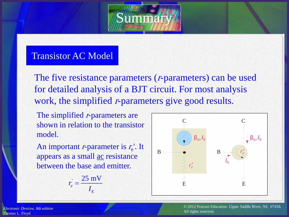
Transistor AC Model
The five resistance parameters (r-parameters) can be used for detailed analysis of a BJT circuit. For most analysis work, the simplified r-parameters give good results.
Summary
βacIb
C
B
E
βacIb
C
B
E
Ib ′re
′re
The simplified r-parameters are shown in relation to the transistor model. An important r-parameter is re'. It appears as a small ac resistance between the base and emitter.
'
E
25 mVer I
=

© 2012 Pearson Education. Upper Saddle River, NJ, 07458. All rights reserved.
Electronic Devices, 9th edition Thomas L. Floyd
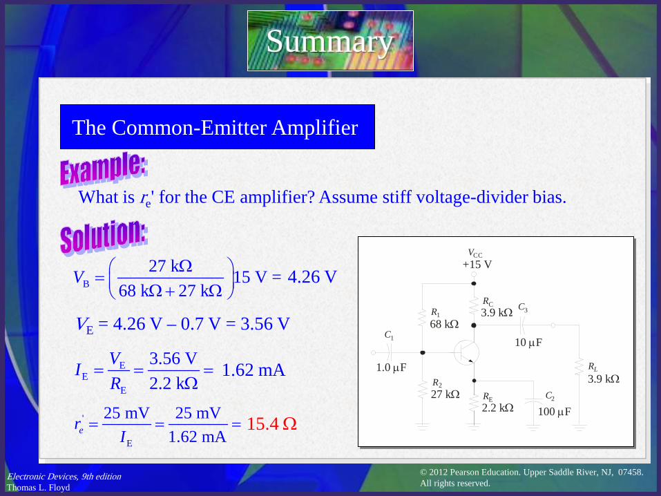
The Common-Emitter Amplifier
In the common-emitter (CE) amplifier, the input signal is applied to the base and the inverted output is taken from the collector. The emitter is common to ac signals.
Summary
R2
RE
R1
Vin
RC
VCC
Vout
RL
C1
C2
C3
© 2012 Pearson Education. Upper Saddle River, NJ, 07458. All rights reserved.
Electronic Devices, 9th edition Thomas L. Floyd
The Common-Emitter Amplifier
Summary
R2
RE
R1
RC
VCC
RL
C1
C2
C3
68 kΩ
27 kΩ2.2 kΩ
3.9 kΩ
3.9 kΩ1.0 Fµ
10 Fµ
100 Fµ
+15 V
What is re' for the CE amplifier? Assume stiff voltage-divider bias.
B27 k 15 V =
68 k 27 kV Ω = Ω + Ω
4.26 V
VE = 4.26 V – 0.7 V = 3.56 V
EE
E
3.56 V2.2 k
VIR
= = =Ω
1.62 mA
'
E
25 mV 25 mV1.62 mAer I
= = = 15.4 Ω
© 2012 Pearson Education. Upper Saddle River, NJ, 07458. All rights reserved.
Electronic Devices, 9th edition Thomas L. Floyd
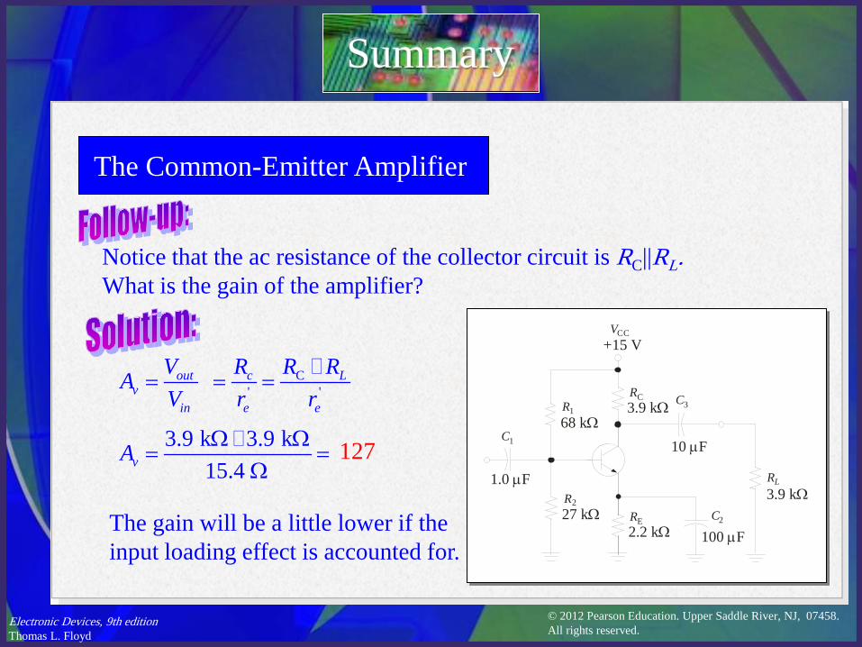
The Common-Emitter Amplifier
Summary
R2
RE
R1
RC
VCC
RL
C1
C2
C3
68 kΩ
27 kΩ2.2 kΩ
3.9 kΩ
3.9 kΩ1.0 Fµ
10 Fµ
100 Fµ
+15 V
What is the gain of the amplifier?
C' ' out c L
vin e e
V R R RAV r r
= = =
127
Notice that the ac resistance of the collector circuit is RC||RL.
3.9 k 3.9 k15.4 vA Ω Ω
= =Ω
The gain will be a little lower if the input loading effect is accounted for.
© 2012 Pearson Education. Upper Saddle River, NJ, 07458. All rights reserved.
Electronic Devices, 9th edition Thomas L. Floyd
The Common-Emitter Amplifier
Summary
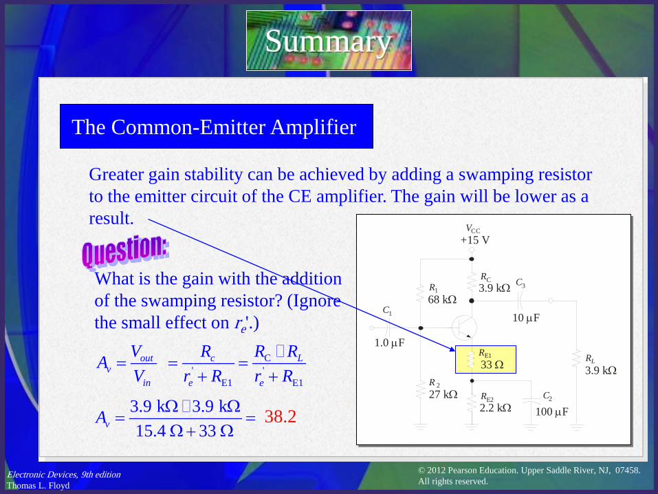
Greater gain stability can be achieved by adding a swamping resistor to the emitter circuit of the CE amplifier. The gain will be lower as a result.
R 2
R
R
E2
E1
R1
RC
VCC
RL
C1
C2
C3
68 kΩ
27 kΩ2.2 kΩ
3.9 kΩ
3.9 kΩ
1.0 Fµ
10 Fµ
100 Fµ
+15 V
33 Ω
What is the gain with the addition of the swamping resistor? (Ignore the small effect on re'.)
C' '
E1 E1
out c Lv
in e e
V R R RAV r R r R
= = =+ +
38.2 3.9 k 3.9 k15.4 33 vA Ω Ω
= =Ω + Ω
© 2012 Pearson Education. Upper Saddle River, NJ, 07458. All rights reserved.
Electronic Devices, 9th edition Thomas L. Floyd
The Common-Emitter Amplifier
Summary
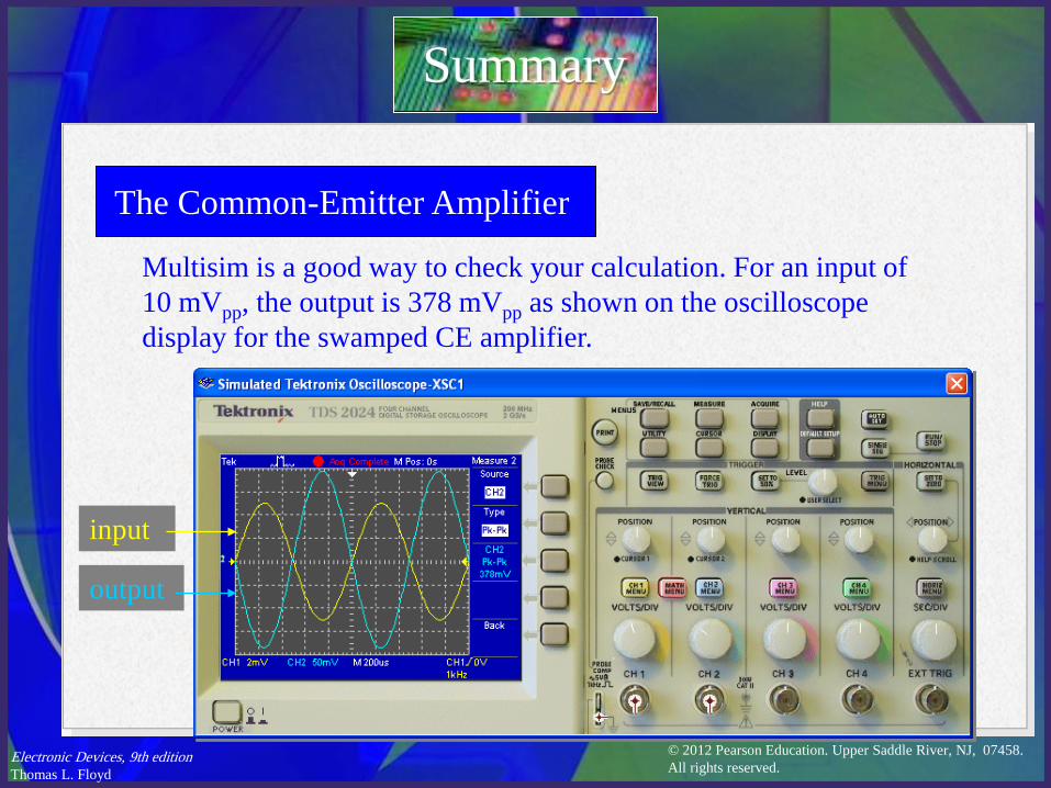
Multisim is a good way to check your calculation. For an input of 10 mVpp, the output is 378 mVpp as shown on the oscilloscope display for the swamped CE amplifier.
input
output
© 2012 Pearson Education. Upper Saddle River, NJ, 07458. All rights reserved.
Electronic Devices, 9th edition Thomas L. Floyd
The Common-Emitter Amplifier
Summary
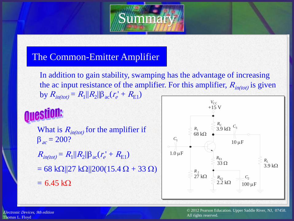
In addition to gain stability, swamping has the advantage of increasing the ac input resistance of the amplifier. For this amplifier, Rin(tot) is given by
R 2
R
R
E2
E1
R1
RC
VCC
RL
C1
C2
C3
68 kΩ
27 kΩ2.2 kΩ
3.9 kΩ
3.9 kΩ
1.0 Fµ
10 Fµ
100 Fµ
+15 V
33 Ω
Rin(tot) = R1||R2||βac(re' + RE1)
What is Rin(tot) for the amplifier if βac = 200?
Rin(tot) = R1||R2||βac(re' + RE1)
= 68 kΩ||27 kΩ||200(15.4 Ω + 33 Ω)
= 6.45 kΩ
© 2012 Pearson Education. Upper Saddle River, NJ, 07458. All rights reserved.
Electronic Devices, 9th edition Thomas L. Floyd
The Common-Collector Amplifier
Summary
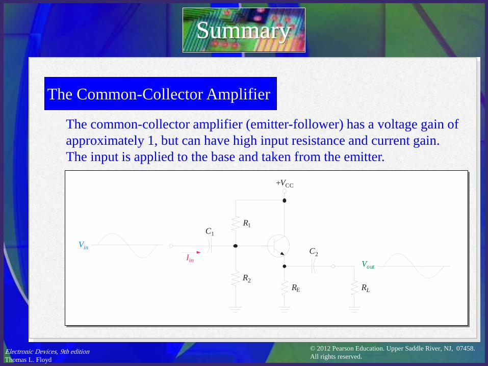
The common-collector amplifier (emitter-follower) has a voltage gain of approximately 1, but can have high input resistance and current gain. The input is applied to the base and taken from the emitter.
+VCC
R1
R2RE RL
Vin
Iin Vout
C1
C2

© 2012 Pearson Education. Upper Saddle River, NJ, 07458. All rights reserved.
Electronic Devices, 9th edition Thomas L. Floyd
The Common-Collector Amplifier
Summary
The power gain is the ratio of the power delivered to the input resistance divided by the power dissipated in the load. This is approximately equal to the current gain. That is, Ap ≈Ai.
Vin
Vout
C1
R1
VCC
R2
RLRE
C2
You can also write power gain as a ratio of resistances:
2
( )22
( )
( ) ( )1
Lin totL L
p vinin L
in tot
in tot in tot
L L
VRP RA A
VP RR
R RR R
= = =
≅ =
The next slide is an example…
© 2012 Pearson Education. Upper Saddle River, NJ, 07458. All rights reserved.
Electronic Devices, 9th edition Thomas L. Floyd
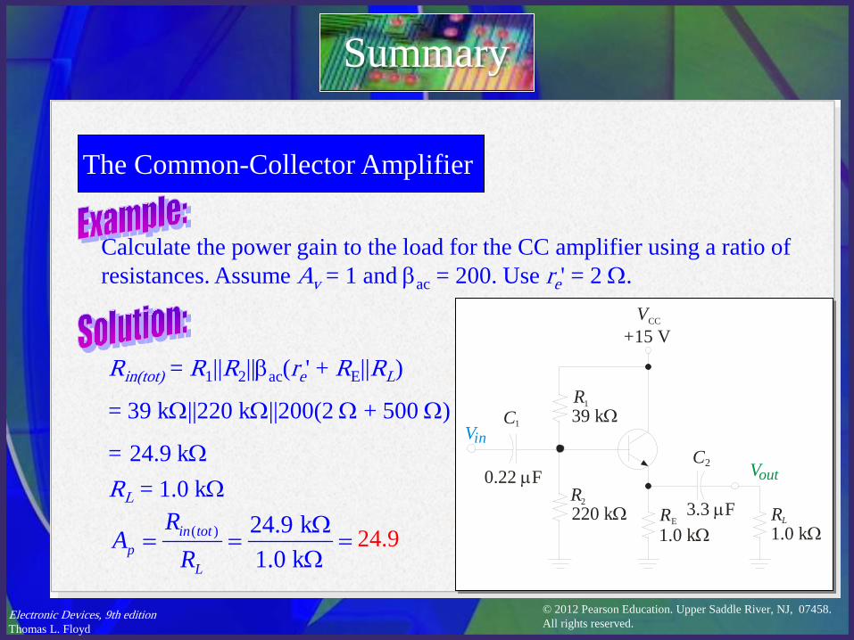
The Common-Collector Amplifier
Summary
Calculate the power gain to the load for the CC amplifier using a ratio of resistances. Assume Av = 1 and βac = 200. Use re' = 2 Ω.
Rin(tot) = R1||R2||βac(re' + RE||RL)
= 39 kΩ||220 kΩ||200(2 Ω + 500 Ω)
= 24.9 kΩ Vin
Vout
C1
R1
VCC
R2
RLRE
C20.22 Fµ
3.3 Fµ
+15 V
39 kΩ
220 kΩ1.0 kΩ 1.0 kΩ
RL = 1.0 kΩ
( ) 24.9 k1.0 k
in totp
L
RA
RΩ
= = =Ω
24.9

© 2012 Pearson Education. Upper Saddle River, NJ, 07458. All rights reserved.
Electronic Devices, 9th edition Thomas L. Floyd
The Common-Collector Amplifier
Summary
The input voltage-divider in the previous example is not “rock-solid” but the overall power gain is good. A “rock solid” stiff voltage-divider is not always the best design. Can you spot the problem illustrated here? Rin(tot) = R1||R2||βac(re' + RE||RL)
= 10 kΩ||10 kΩ||200(25 Ω + 3.0 kΩ)
= 4.96 kΩ RL = 10 kΩ
( ) 4.96 k10 k
in totp
L
RA
RΩ
= = =Ω
0.496!
Vin
Vout
C1
R1
VCC
R2
RLRE
C2
10 kΩ
10 kΩ10 kΩ
4.3 kΩ
+10 V
β = 200
The problem is the power gain is less than 1!
© 2012 Pearson Education. Upper Saddle River, NJ, 07458. All rights reserved.
Electronic Devices, 9th edition Thomas L. Floyd
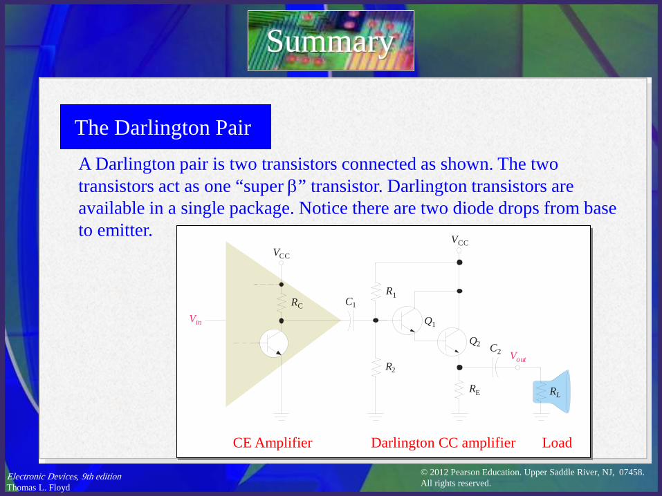
The Darlington Pair
Summary
A Darlington pair is two transistors connected as shown. The two transistors act as one “super β” transistor. Darlington transistors are available in a single package. Notice there are two diode drops from base to emitter. VCC
R1
C2
R2
RE RL
Vin
Q2
Q1
VCC
RC C1
Vout
CE Amplifier Darlington CC amplifier Load
© 2012 Pearson Education. Upper Saddle River, NJ, 07458. All rights reserved.
Electronic Devices, 9th edition Thomas L. Floyd
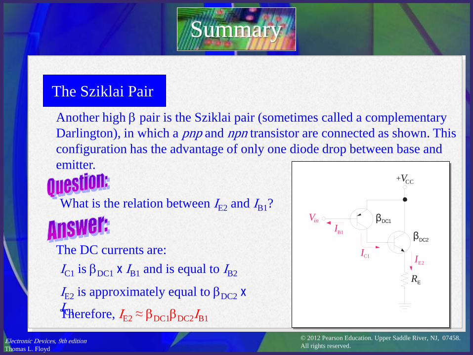
The Sziklai Pair
Summary
Another high β pair is the Sziklai pair (sometimes called a complementary Darlington), in which a pnp and npn transistor are connected as shown. This configuration has the advantage of only one diode drop between base and emitter.
+VCC
RE
βDC1
βDC2
IB1
IC1 IE2
Vin
IC1 is βDC1 x IB1 and is equal to IB2
IE2 is approximately equal to βDC2 x IC1 Therefore, IE2 ≈ βDC1βDC2IB1
The DC currents are:
What is the relation between IE2 and IB1?
© 2012 Pearson Education. Upper Saddle River, NJ, 07458. All rights reserved.
Electronic Devices, 9th edition Thomas L. Floyd
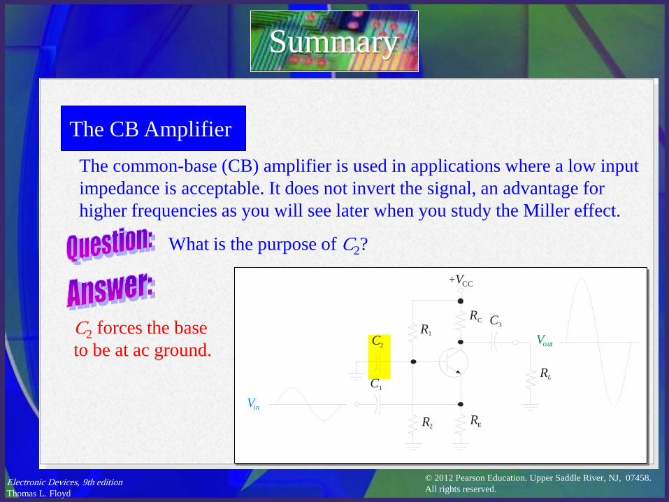
The CB Amplifier
Summary
The common-base (CB) amplifier is used in applications where a low input impedance is acceptable. It does not invert the signal, an advantage for higher frequencies as you will see later when you study the Miller effect.
C2 forces the base to be at ac ground.
What is the purpose of C2?
+VCC
R1
RC
RE
RL
R2
C2
C3
C1
Vin
Vout
© 2012 Pearson Education. Upper Saddle River, NJ, 07458. All rights reserved.
Electronic Devices, 9th edition Thomas L. Floyd
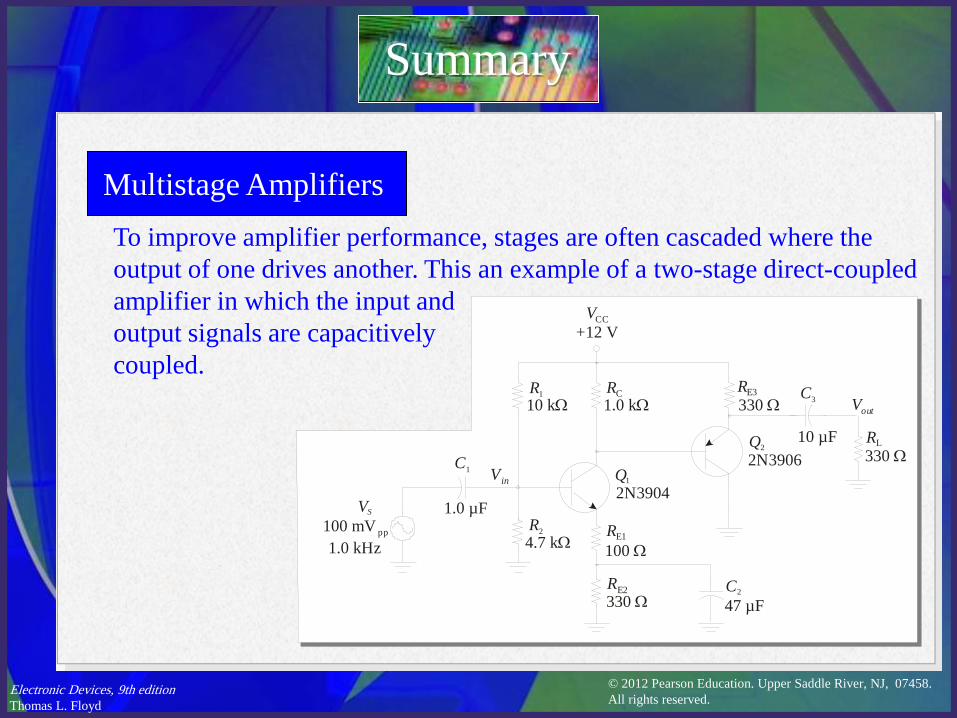
Multistage Amplifiers
Summary
To improve amplifier performance, stages are often cascaded where the output of one drives another. This an example of a two-stage direct-coupled amplifier in which the input and output signals are capacitively coupled.
Q1
Q2
VCC+12 V
Vin
Vout
VS
100 mV1.0 kHz
pp
RE3
RE1
RE2
RCR1
R2
C1
C2
C3
RL
1.0 kΩ
1.0 µF
47 µF
100 Ω
330 Ω
2N3904
330 Ω
10 µF330 Ω2N3906
10 kΩ
4.7 kΩ
© 2012 Pearson Education. Upper Saddle River, NJ, 07458. All rights reserved.
Electronic Devices, 9th edition Thomas L. Floyd
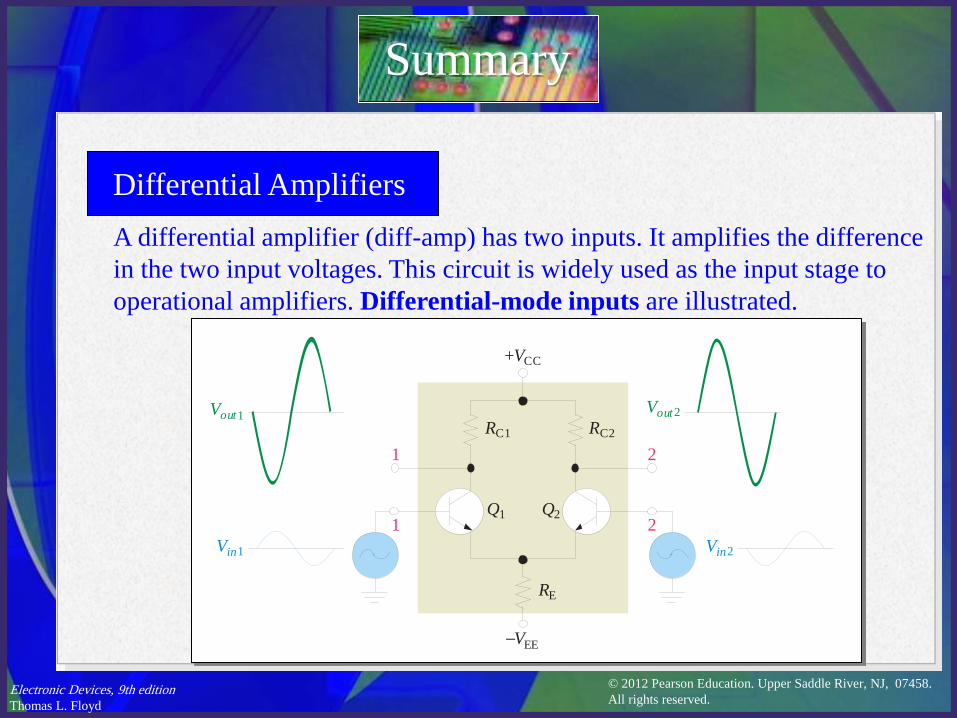
Differential Amplifiers
Summary
A differential amplifier (diff-amp) has two inputs. It amplifies the difference in the two input voltages. This circuit is widely used as the input stage to operational amplifiers. Differential-mode inputs are illustrated.
+VCC
RC1 RC2
Q1 Q2
–VEE
RE
1 2
21
Vout1
Vin1 Vin2
Vout2
© 2012 Pearson Education. Upper Saddle River, NJ, 07458. All rights reserved.
Electronic Devices, 9th edition Thomas L. Floyd
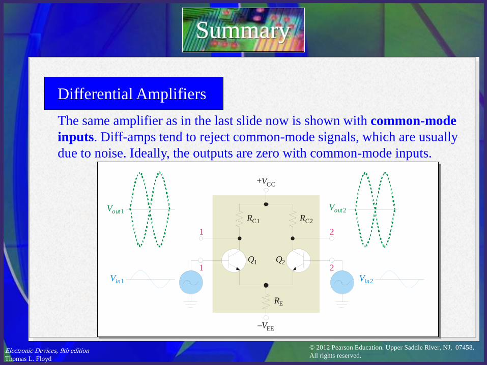
Differential Amplifiers
Summary
The same amplifier as in the last slide now is shown with common-mode inputs. Diff-amps tend to reject common-mode signals, which are usually due to noise. Ideally, the outputs are zero with common-mode inputs.
+VCC
RC1 RC2
Q1 Q2
–VEE
RE
1 2
21
Vout1
Vin1 Vin2
Vout2
© 2012 Pearson Education. Upper Saddle River, NJ, 07458. All rights reserved.
Electronic Devices, 9th edition Thomas L. Floyd
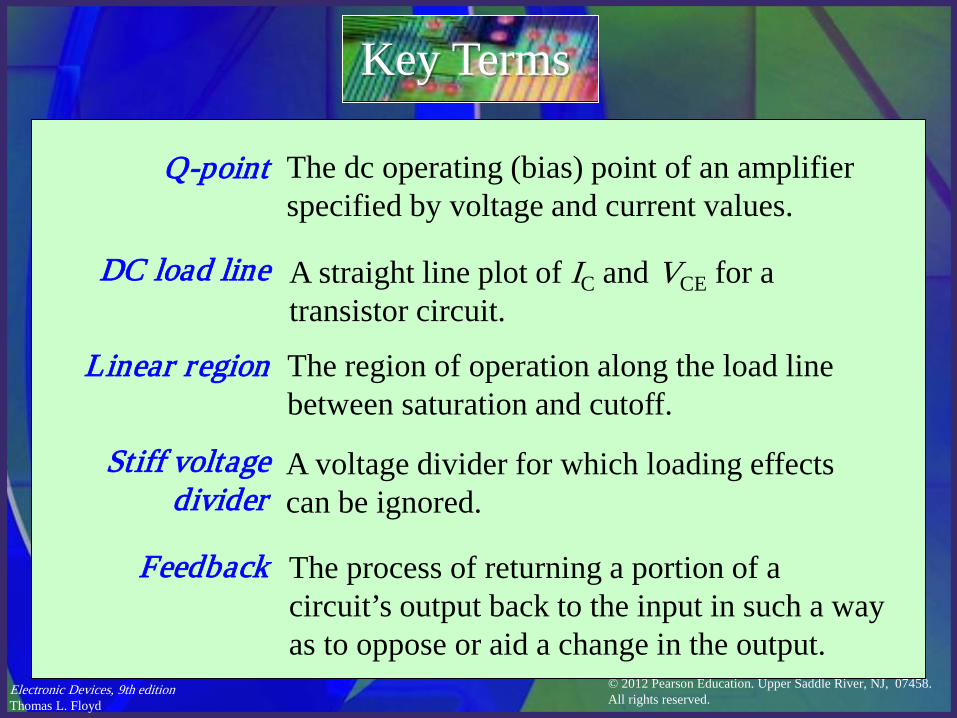
Key Terms
Q-point
DC load line
Linear region
Stiff voltage divider
Feedback
The dc operating (bias) point of an amplifier specified by voltage and current values.
A straight line plot of IC and VCE for a transistor circuit.
The region of operation along the load line between saturation and cutoff.
A voltage divider for which loading effects can be ignored.
The process of returning a portion of a circuit’s output back to the input in such a way as to oppose or aid a change in the output.
© 2012 Pearson Education. Upper Saddle River, NJ, 07458. All rights reserved.
Electronic Devices, 9th edition Thomas L. Floyd
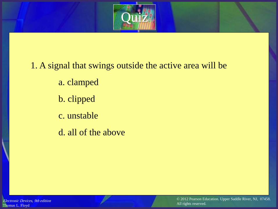
Quiz
1. A signal that swings outside the active area will be
a. clamped
b. clipped
c. unstable
d. all of the above

© 2012 Pearson Education. Upper Saddle River, NJ, 07458. All rights reserved.
Electronic Devices, 9th edition Thomas L. Floyd
Quiz
2. A stiff voltage divider is one in which
a. there is no load current
b. divider current is small compared to load current
c. the load is connected directly to the source voltage
d. loading effects can be ignored
© 2012 Pearson Education. Upper Saddle River, NJ, 07458. All rights reserved.
Electronic Devices, 9th edition Thomas L. Floyd
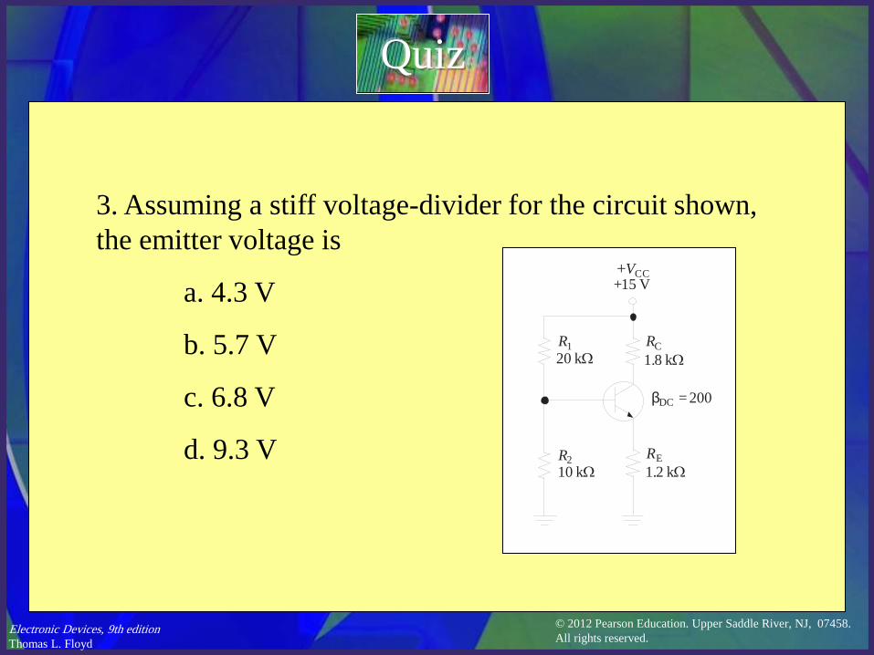
Quiz
3. Assuming a stiff voltage-divider for the circuit shown, the emitter voltage is
a. 4.3 V
b. 5.7 V
c. 6.8 V
d. 9.3 V
+VCC
RCR1
RER2
βDC = 200
20 kΩ
10 kΩ
+15 V
1.2 kΩ
1.8 kΩ
© 2012 Pearson Education. Upper Saddle River, NJ, 07458. All rights reserved.
Electronic Devices, 9th edition Thomas L. Floyd
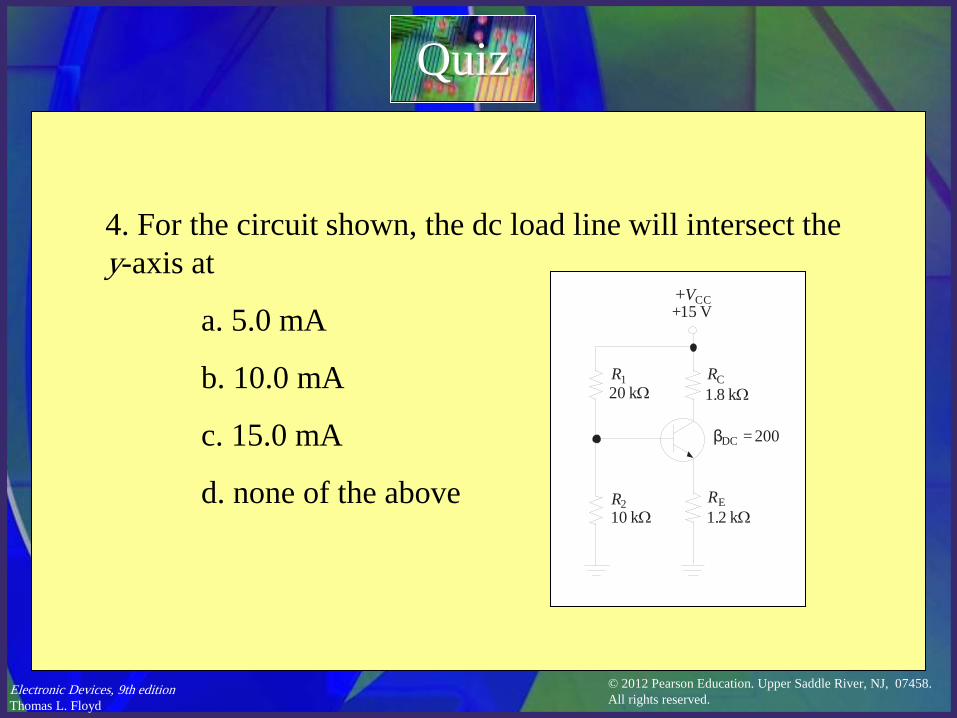
Quiz
4. For the circuit shown, the dc load line will intersect the y-axis at
a. 5.0 mA
b. 10.0 mA
c. 15.0 mA
d. none of the above
+VCC
RCR1
RER2
βDC = 200
20 kΩ
10 kΩ
+15 V
1.2 kΩ
1.8 kΩ
© 2012 Pearson Education. Upper Saddle River, NJ, 07458. All rights reserved.
Electronic Devices, 9th edition Thomas L. Floyd
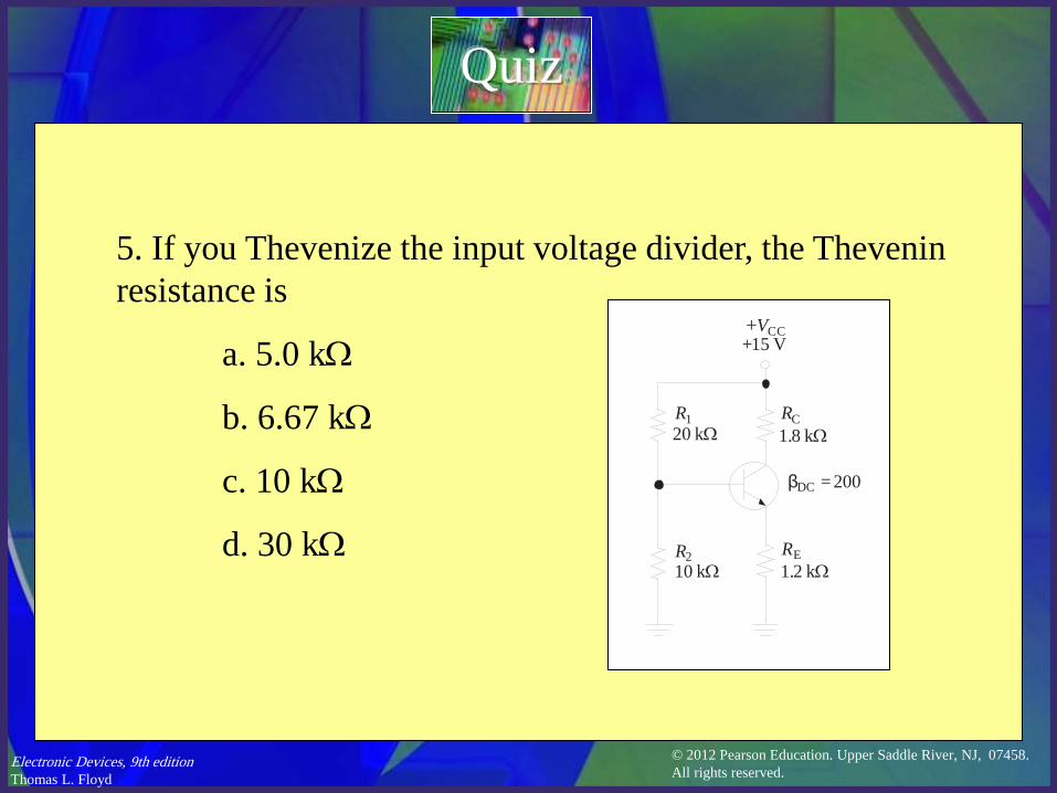
Quiz
5. If you Thevenize the input voltage divider, the Thevenin resistance is
a. 5.0 kΩ
b. 6.67 kΩ
c. 10 kΩ
d. 30 kΩ
+VCC
RCR1
RER2
βDC = 200
20 kΩ
10 kΩ
+15 V
1.2 kΩ
1.8 kΩ
© 2012 Pearson Education. Upper Saddle River, NJ, 07458. All rights reserved.
Electronic Devices, 9th edition Thomas L. Floyd
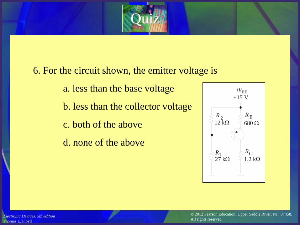
Quiz
6. For the circuit shown, the emitter voltage is
a. less than the base voltage
b. less than the collector voltage
c. both of the above
d. none of the above
+VEE
R 2
1R RC1.2 kΩ
R E680 Ω
27 kΩ
12 kΩ
+15 V
© 2012 Pearson Education. Upper Saddle River, NJ, 07458. All rights reserved.
Electronic Devices, 9th edition Thomas L. Floyd
Quiz
7. Emitter bias
a. is not good for linear circuits
b. uses a voltage-divider on the input
c. requires dual power supplies
d. all of the above
© 2012 Pearson Education. Upper Saddle River, NJ, 07458. All rights reserved.
Electronic Devices, 9th edition Thomas L. Floyd
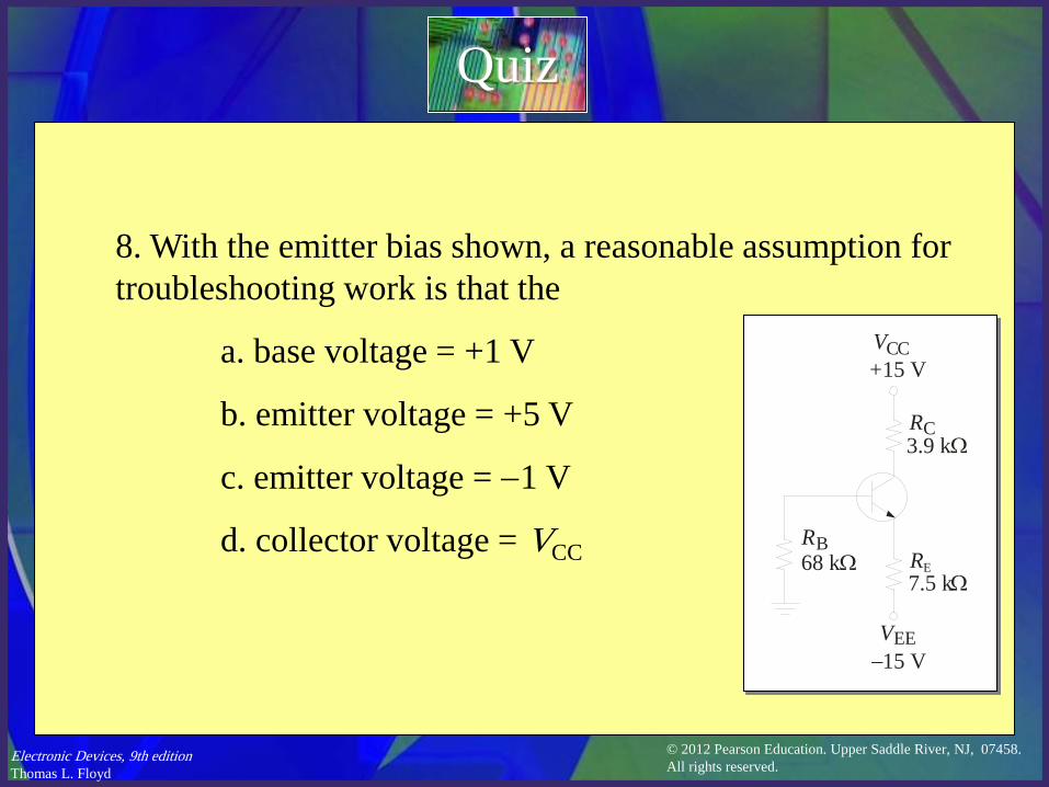
Quiz
8. With the emitter bias shown, a reasonable assumption for troubleshooting work is that the
a. base voltage = +1 V
b. emitter voltage = +5 V
c. emitter voltage = −1 V
d. collector voltage = VCC
V
V
CC
EE
RC
RE
RB68 kΩ
+15 V
−15 V
7.5 kΩ
3.9 kΩ
© 2012 Pearson Education. Upper Saddle River, NJ, 07458. All rights reserved.
Electronic Devices, 9th edition Thomas L. Floyd
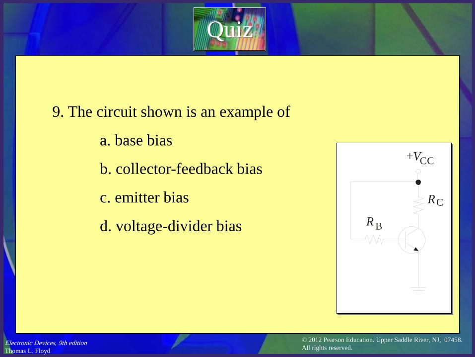
Quiz
9. The circuit shown is an example of
a. base bias
b. collector-feedback bias
c. emitter bias
d. voltage-divider bias
RC
R B
+VCC
© 2012 Pearson Education. Upper Saddle River, NJ, 07458. All rights reserved.
Electronic Devices, 9th edition Thomas L. Floyd
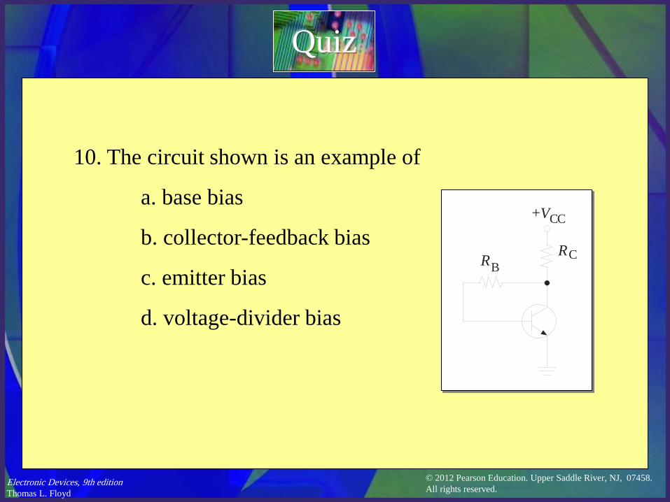
Quiz
10. The circuit shown is an example of
a. base bias
b. collector-feedback bias
c. emitter bias
d. voltage-divider bias
+VCC
RCRB
© 2012 Pearson Education. Upper Saddle River, NJ, 07458. All rights reserved.
Electronic Devices, 9th edition Thomas L. Floyd
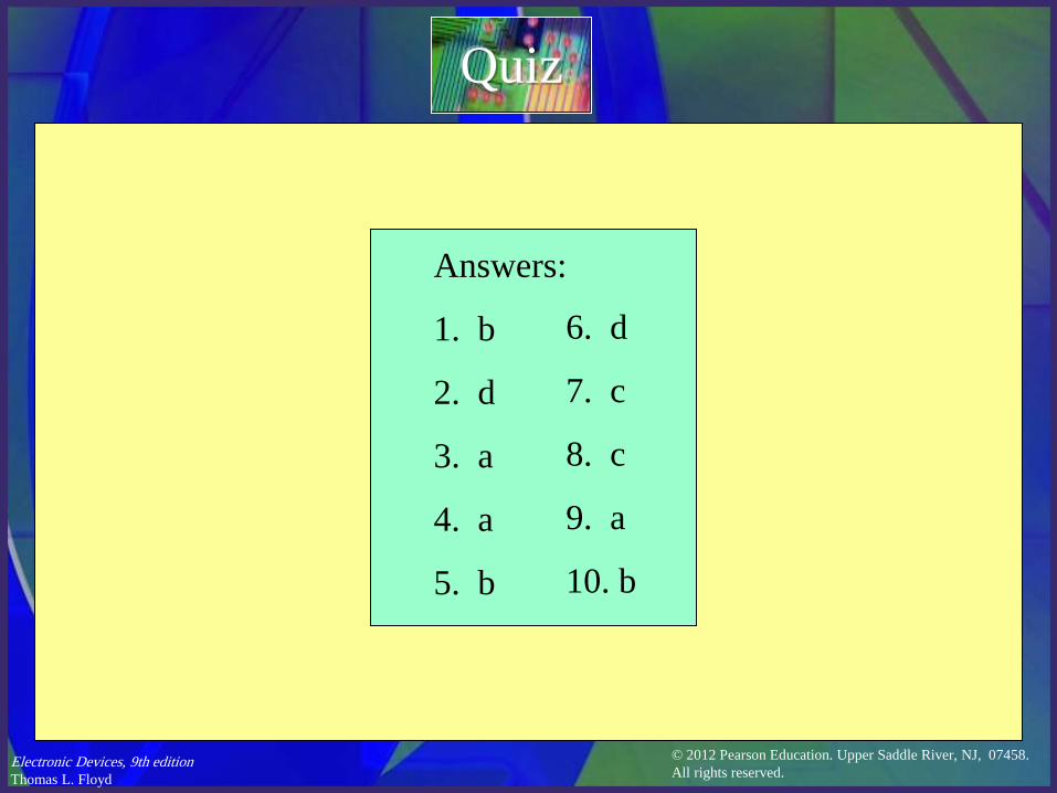
Quiz
Answers:
1. b
2. d
3. a
4. a
5. b
6. d
7. c
8. c
9. a
10. b