electronic-devices-9th-edition-by-floyd pp12a
36
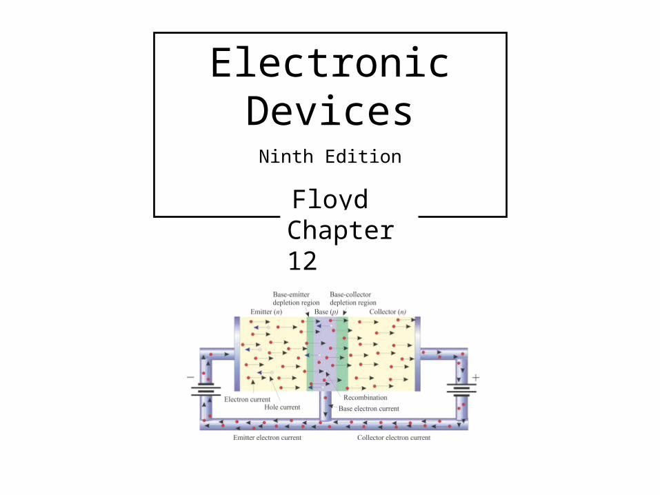
© 2012 Pearson Education. Upper Saddle River, NJ, 07458. All rights reserved. Electronic Devices, 9th edition Thomas L. Floyd Electronic Devices Ninth Edition Floyd Chapter 12
-
Upload
pinitnai-sittithai -
Category
Education
-
view
424 -
download
97
Transcript of electronic-devices-9th-edition-by-floyd pp12a
© 2012 Pearson Education. Upper Saddle River, NJ, 07458. All rights reserved.
Electronic Devices, 9th editionThomas L. Floyd
Electronic DevicesNinth Edition
Floyd
Chapter 12
© 2012 Pearson Education. Upper Saddle River, NJ, 07458. All rights reserved.
Electronic Devices, 9th editionThomas L. Floyd
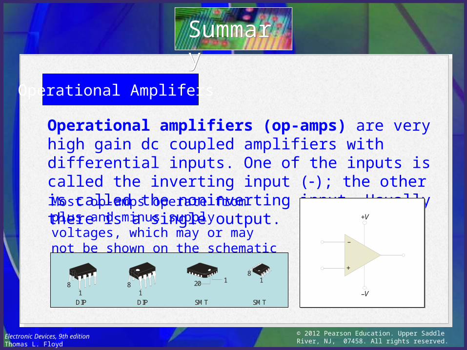
Operational Amplifers
Operational amplifiers (op-amps) are very high gain dc coupled amplifiers with differential inputs. One of the inputs is called the inverting input (); the other is called the noninverting input. Usually there is a single output.Most op-amps operate from plus and minus supply voltages, which may or may not be shown on the schematic symbol.
SummarySummary
–
+
+V
–V
1201
8
DIP1
8
DIP SMT
18
SMT
© 2012 Pearson Education. Upper Saddle River, NJ, 07458. All rights reserved.
Electronic Devices, 9th editionThomas L. Floyd
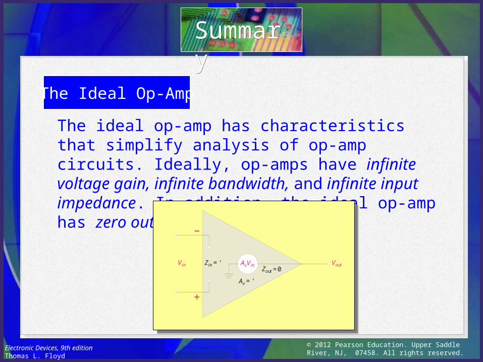
The Ideal Op-Amp
The ideal op-amp has characteristics that simplify analysis of op-amp circuits. Ideally, op-amps have infinite voltage gain, infinite bandwidth, and infinite input impedance. In addition, the ideal op-amp has zero output impedance.
SummarySummary
–
+
Zin = ‘Vin VoutZout = 0
AvVin
Av = ‘
© 2012 Pearson Education. Upper Saddle River, NJ, 07458. All rights reserved.
Electronic Devices, 9th editionThomas L. Floyd
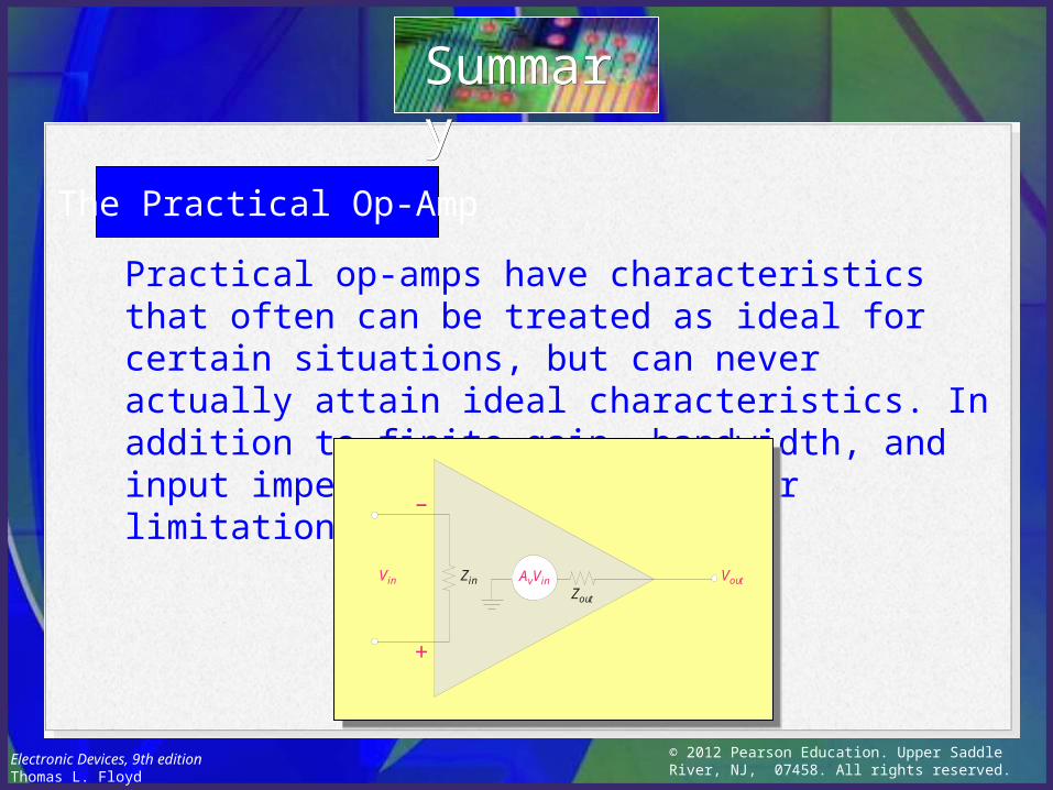
The Practical Op-Amp
Practical op-amps have characteristics that often can be treated as ideal for certain situations, but can never actually attain ideal characteristics. In addition to finite gain, bandwidth, and input impedance, they have other limitations.
SummarySummary
–
+
ZinVin VoutZout
AvVin
© 2012 Pearson Education. Upper Saddle River, NJ, 07458. All rights reserved.
Electronic Devices, 9th editionThomas L. Floyd
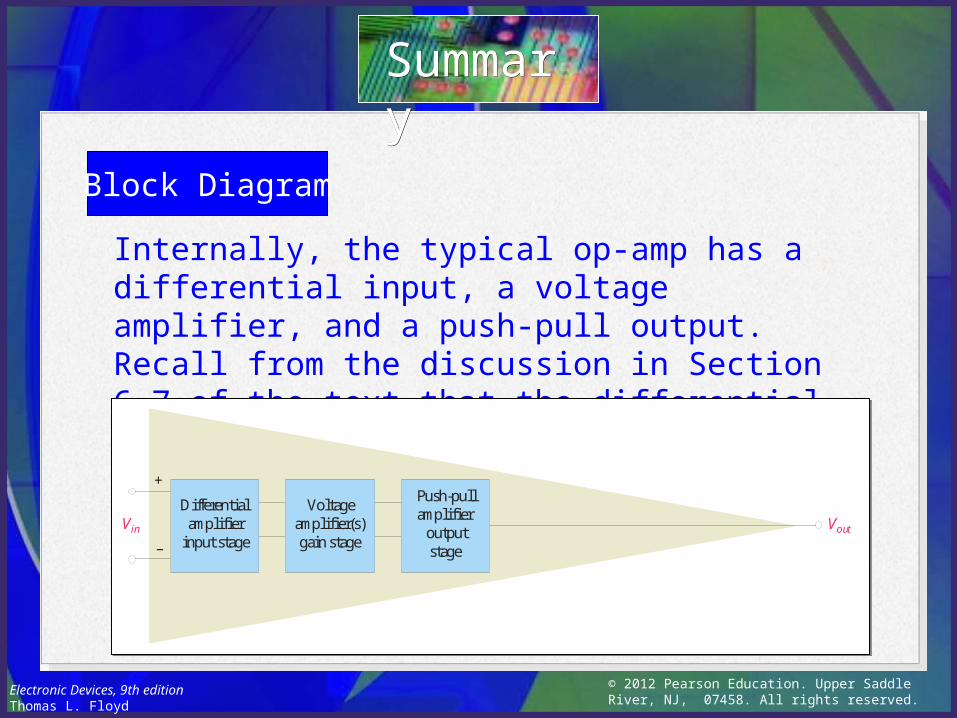
Block Diagram
Internally, the typical op-amp has a differential input, a voltage amplifier, and a push-pull output. Recall from the discussion in Section 6-7 of the text that the differential amplifier amplifies the difference in the two inputs.
SummarySummary
Differentialamplifier
input stage
Voltageamplifier(s)gain stage
Push-pullamplifier
outputstage
Vin Vout
+
–
© 2012 Pearson Education. Upper Saddle River, NJ, 07458. All rights reserved.
Electronic Devices, 9th editionThomas L. Floyd
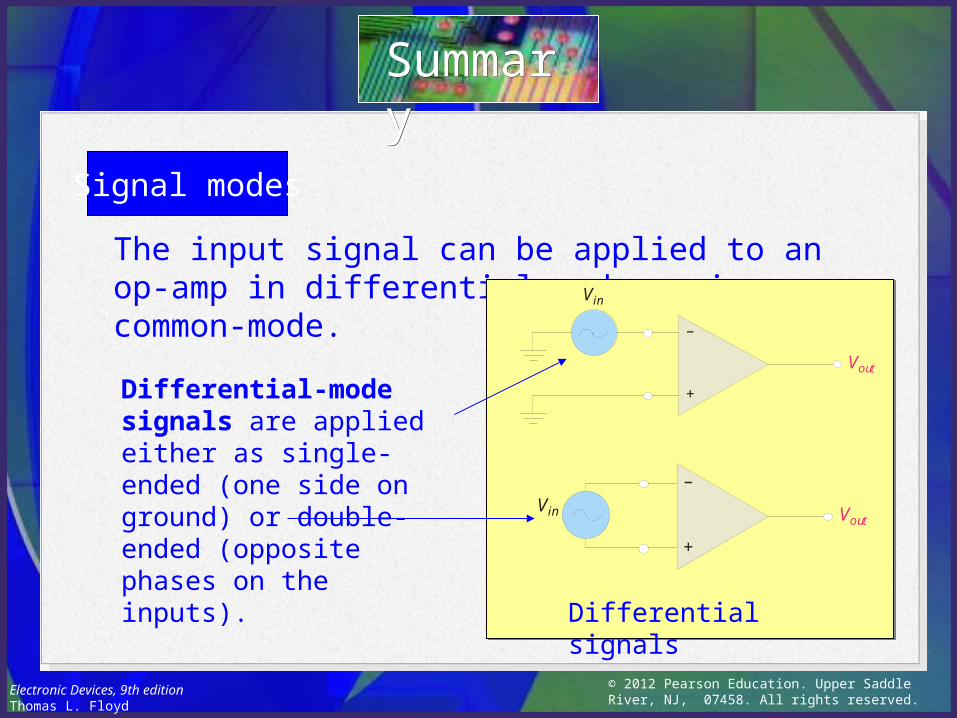
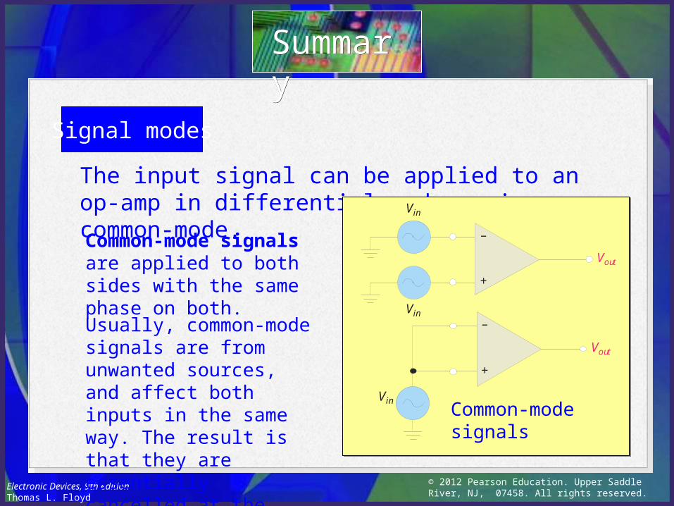
Signal modes
The input signal can be applied to an op-amp in differential-mode or in common-mode.
SummarySummary
Differential-mode signals are applied either as single-ended (one side on ground) or double-ended (opposite phases on the inputs).
Vin
–
+
Vout
Vin
–
+
Vout
Differential signals
© 2012 Pearson Education. Upper Saddle River, NJ, 07458. All rights reserved.
Electronic Devices, 9th editionThomas L. Floyd
Signal modes
The input signal can be applied to an op-amp in differential-mode or in common-mode.
SummarySummary
Common-mode signals are applied to both sides with the same phase on both.
Vin
Vin
–
+
Vout
Vin
–
+
Vout
Usually, common-mode signals are from unwanted sources, and affect both inputs in the same way. The result is that they are essentially cancelled at the output.
Common-mode signals
© 2012 Pearson Education. Upper Saddle River, NJ, 07458. All rights reserved.
Electronic Devices, 9th editionThomas L. Floyd
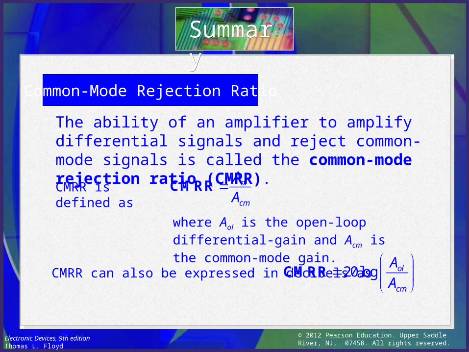
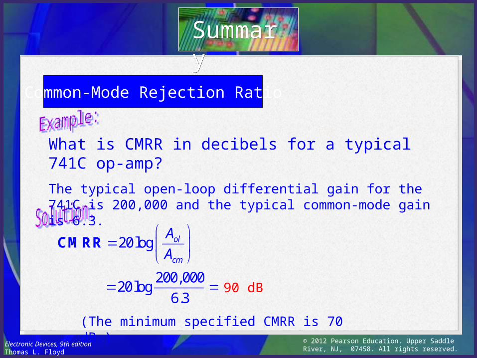
Common-Mode Rejection Ratio
The ability of an amplifier to amplify differential signals and reject common-mode signals is called the common-mode rejection ratio (CMRR).
SummarySummary
CMRR is defined as ol
cm
AA
CMRR
where Aol is the open-loop differential-gain and Acm is the common-mode gain.
CMRR can also be expressed in decibels as 20log ol
cm
AA
CMRR
© 2012 Pearson Education. Upper Saddle River, NJ, 07458. All rights reserved.
Electronic Devices, 9th editionThomas L. Floyd
Common-Mode Rejection Ratio
SummarySummary
What is CMRR in decibels for a typical 741C op-amp? The typical open-loop differential gain for the 741C is 200,000 and the typical common-mode gain is 6.3.
90 dB
20log ol
cm
AA
CMRR
200,00020log6.3
(The minimum specified CMRR is 70 dB.)
© 2012 Pearson Education. Upper Saddle River, NJ, 07458. All rights reserved.
Electronic Devices, 9th editionThomas L. Floyd
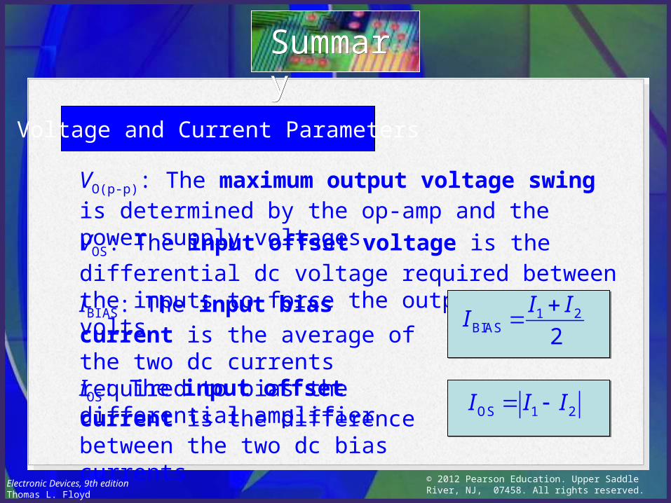
Voltage and Current Parameters
SummarySummary
VO(p-p): The maximum output voltage swing is determined by the op-amp and the power supply voltages VOS: The input offset voltage is the differential dc voltage required between the inputs to force the output to zero volts IBIAS: The input bias current is the average of the two dc currents required to bias the differential amplifierIOS: The input offset current is the difference between the two dc bias currents
1 2BIAS 2
I II
OS 1 2I I I
© 2012 Pearson Education. Upper Saddle River, NJ, 07458. All rights reserved.
Electronic Devices, 9th editionThomas L. Floyd
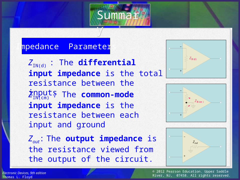
Impedance Parameters
SummarySummary
ZIN(d) : The differential input impedance is the total resistance between the inputs
ZIN(cm) : The common-mode input impedance is the resistance between each input and ground
ZIN(d)
–
+
ZIN(cm)
–
+
Zout: The output impedance is the resistance viewed from the output of the circuit.
Zout
–
+
© 2012 Pearson Education. Upper Saddle River, NJ, 07458. All rights reserved.
Electronic Devices, 9th editionThomas L. Floyd
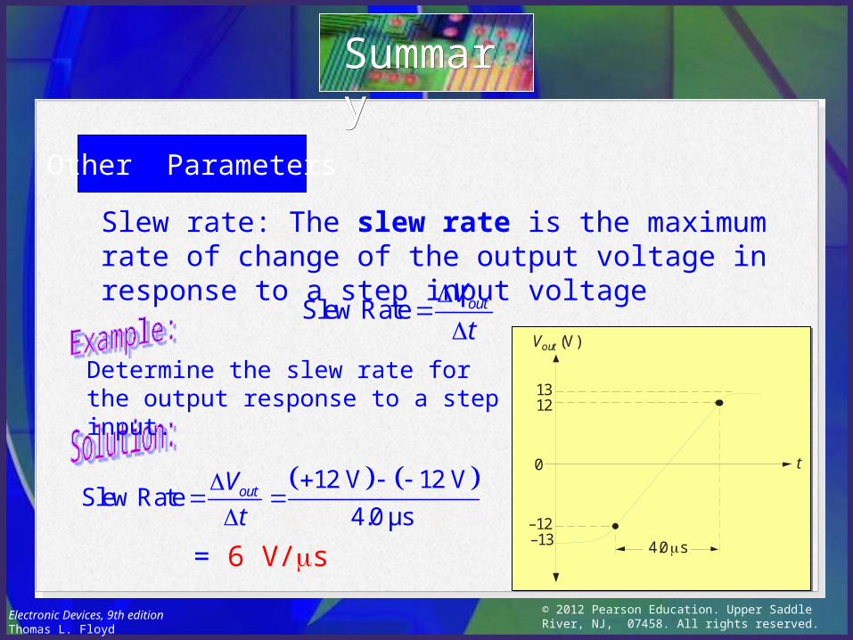
Other Parameters
SummarySummary
Slew rate: The slew rate is the maximum rate of change of the output voltage in response to a step input voltage
Slew Rate outVt
Determine the slew rate for the output response to a step input.
12 V 12 VSlew Rate
4.0 μs outVt
Vout (V)
t
–13–12
1312
0
4.0 sm= 6 V/ms
© 2012 Pearson Education. Upper Saddle River, NJ, 07458. All rights reserved.
Electronic Devices, 9th editionThomas L. Floyd
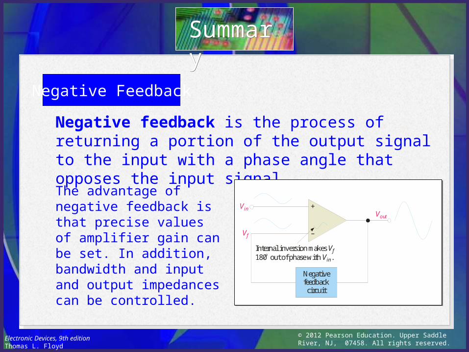
Negative Feedback
SummarySummary
Negative feedback is the process of returning a portion of the output signal to the input with a phase angle that opposes the input signal.
Vout
+
–
Vin
Vf
Internal inversion makes Vf180° out of phase with Vin.
Negativefeedbackcircuit
The advantage of negative feedback is that precise values of amplifier gain can be set. In addition, bandwidth and input and output impedances can be controlled.
© 2012 Pearson Education. Upper Saddle River, NJ, 07458. All rights reserved.
Electronic Devices, 9th editionThomas L. Floyd
Noninverting Amplifier
SummarySummary
A noninverting amplifier is a configuration in which the signal is on the noninverting input and a portion of the output is returned to the inverting input.
Feedback forces Vf to be equal to Vin, hence Vin is across Ri. With basic algebra, you can show that the closed-loop gain of the noninverting amplifier is
Rf
Ri
Vf
Vin
+
–
Feedbackcircuit
Vout
(NI) 1 fcl
i
RA
R
© 2012 Pearson Education. Upper Saddle River, NJ, 07458. All rights reserved.
Electronic Devices, 9th editionThomas L. Floyd
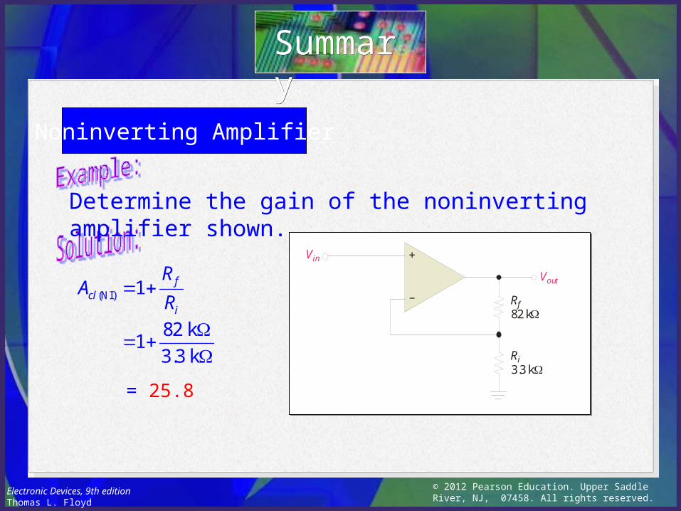
Noninverting Amplifier
SummarySummary
(NI) 1 fcl
i
RA
R
Determine the gain of the noninverting amplifier shown.
Rf82 kW
Vin +
–
Vout
Ri3.3 kW
82 k13.3 k
W
W
= 25.8
© 2012 Pearson Education. Upper Saddle River, NJ, 07458. All rights reserved.
Electronic Devices, 9th editionThomas L. Floyd
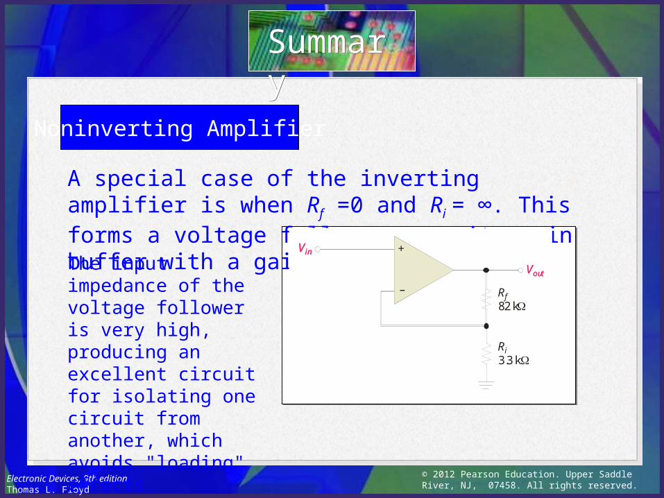
Noninverting Amplifier
SummarySummary
A special case of the inverting amplifier is when Rf =0 and Ri = ∞. This forms a voltage follower or unity gain buffer with a gain of 1.
Rf82 kW
Vin +
–
Vout
Ri3.3 kW
The input impedance of the voltage follower is very high, producing an excellent circuit for isolating one circuit from another, which avoids "loading" effects.
Vin +
–
Vout
© 2012 Pearson Education. Upper Saddle River, NJ, 07458. All rights reserved.
Electronic Devices, 9th editionThomas L. Floyd
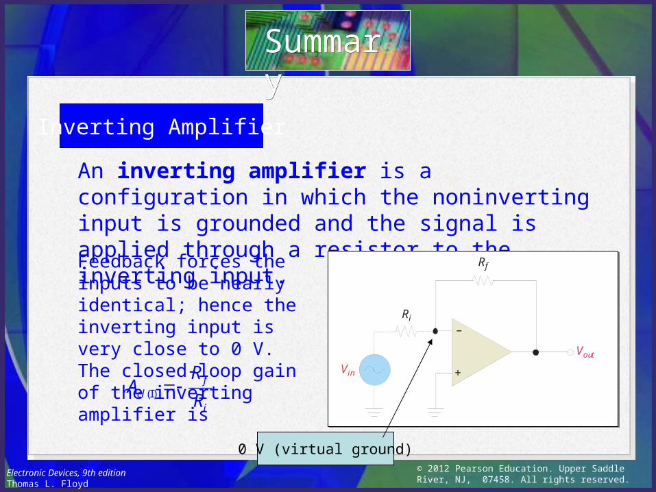
Inverting Amplifier
SummarySummary
An inverting amplifier is a configuration in which the noninverting input is grounded and the signal is applied through a resistor to the inverting input.
Feedback forces the inputs to be nearly identical; hence the inverting input is very close to 0 V. The closed-loop gain of the inverting amplifier is
(I)f
cli
RA
R
–
+
Rf
Vout
Ri
Vin
0 V (virtual ground)
© 2012 Pearson Education. Upper Saddle River, NJ, 07458. All rights reserved.
Electronic Devices, 9th editionThomas L. Floyd
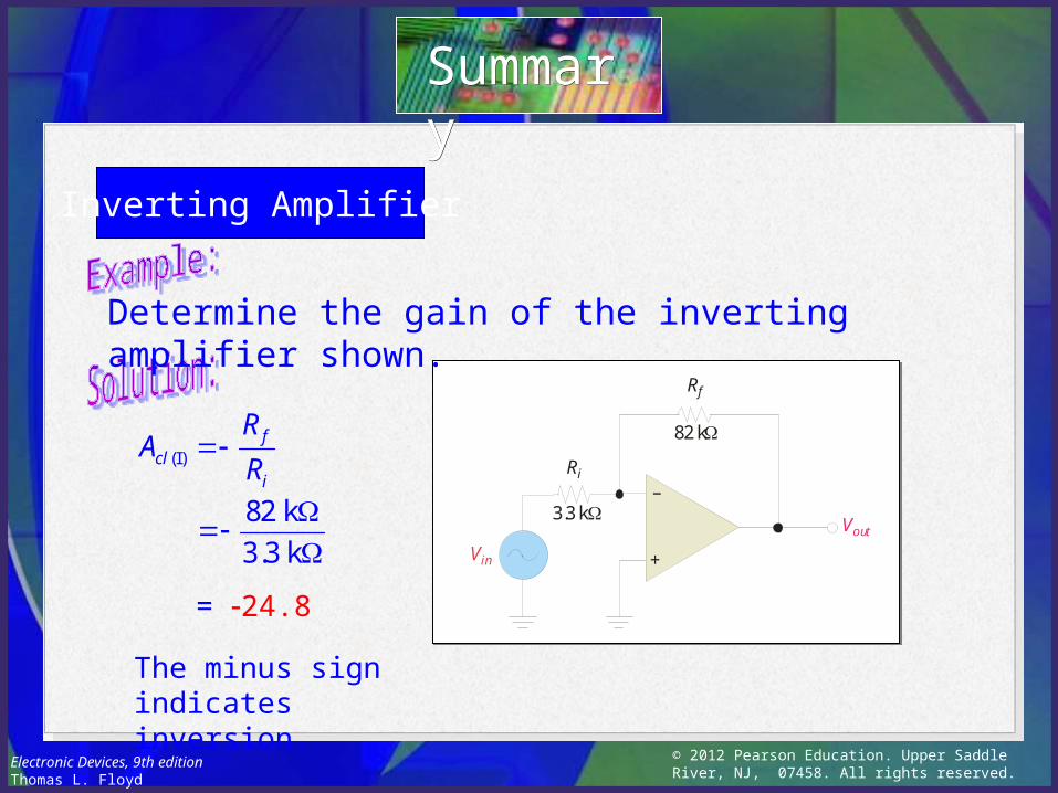
SummarySummary
Determine the gain of the inverting amplifier shown.
82 k3.3 k
W
W
= 24.8
–
+
Rf
Vout
Ri
Vin
82 kW
3.3 kW
(I)f
cli
RA
R
The minus sign indicates inversion.
Inverting Amplifier
© 2012 Pearson Education. Upper Saddle River, NJ, 07458. All rights reserved.
Electronic Devices, 9th editionThomas L. Floyd
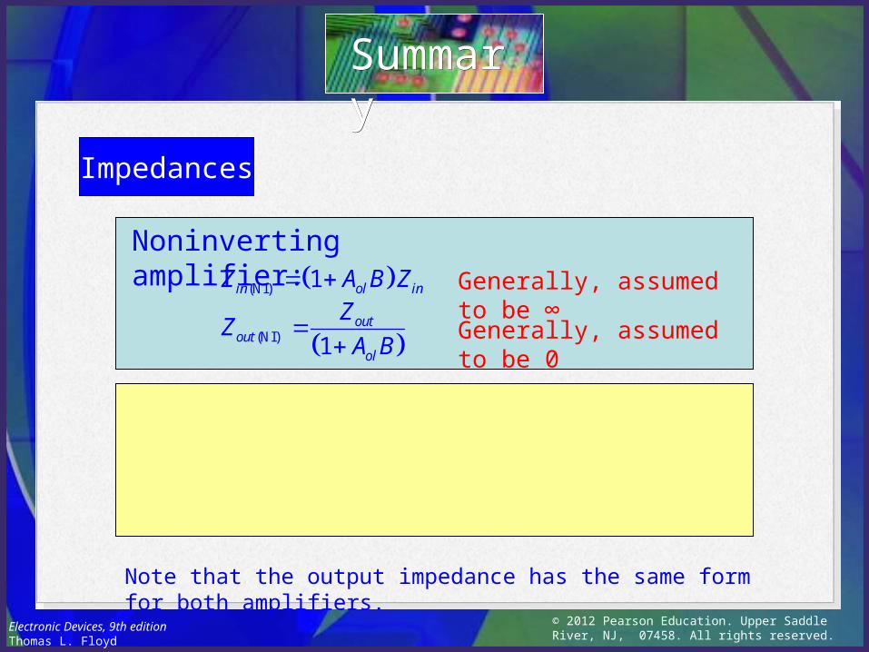
SummarySummary
Noninverting amplifier:
Impedances
(NI) 1in ol inZ A B Z
(NI) 1out
outol
ZZ
A B
Generally, assumed to be ∞
Generally, assumed to be 0
(I) in iZ R
(I) 1out
outol
ZZ
A B
Generally, assumed to be Ri
Generally, assumed to be 0
Inverting amplifier:
Note that the output impedance has the same form for both amplifiers.
© 2012 Pearson Education. Upper Saddle River, NJ, 07458. All rights reserved.
Electronic Devices, 9th editionThomas L. Floyd
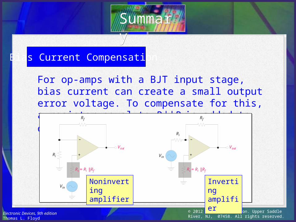
SummarySummary
Bias Current Compensation
For op-amps with a BJT input stage, bias current can create a small output error voltage. To compensate for this, a resistor equal to Ri||Rf is added to one of the inputs.
–
+
Rf
Vout
Ri
Vin
Rc = Ri || Rf
–
+
Rf
Vout
Ri
Vin
Rc = Ri || Rf
Noninverting amplifier
Inverting amplifier
© 2012 Pearson Education. Upper Saddle River, NJ, 07458. All rights reserved.
Electronic Devices, 9th editionThomas L. Floyd
SummarySummary
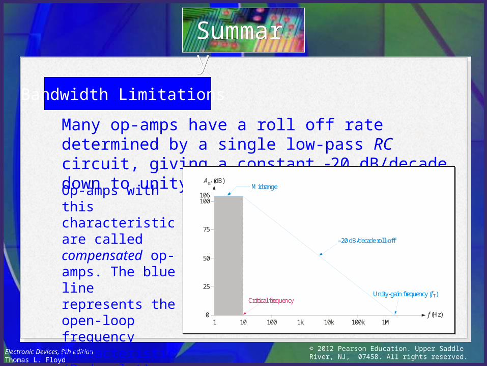
Bandwidth Limitations
Many op-amps have a roll off rate determined by a single low-pass RC circuit, giving a constant 20 dB/decade down to unity gain.
–20 dB/decade roll-off
Unity-gain frequency (fT)Critical frequency
101 100 1k 10k 100k 1Mf (Hz)
106100
75
50
25
0
Aol (dB)MidrangeOp-amps with this
characteristic are called compensated op-amps. The blue line represents the open-loop frequency characteristic (Bode plot) for the op-amp.
© 2012 Pearson Education. Upper Saddle River, NJ, 07458. All rights reserved.
Electronic Devices, 9th editionThomas L. Floyd
SummarySummary
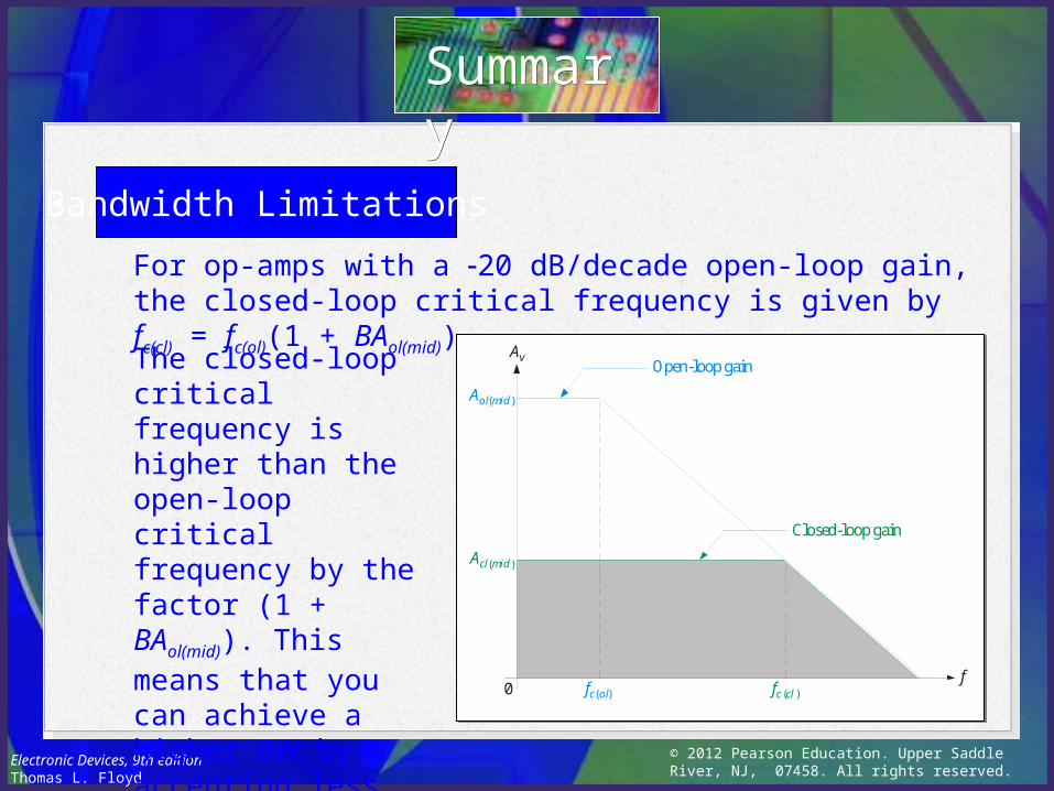
Bandwidth Limitations
For op-amps with a 20 dB/decade open-loop gain, the closed-loop critical frequency is given by fc(cl) = fc(ol)(1 + BAol(mid))
The closed-loop critical frequency is higher than the open-loop critical frequency by the factor (1 + BAol(mid)). This means that you can achieve a higher BW by accepting less gain. For a compensated op-amp, Acl f(cl) = Aol fc(ol).
.
Av
f
Aol(mid )
0 fc(ol) fc (cl )
Acl(mid )
Closed-loop gain
Open-loop gain
© 2012 Pearson Education. Upper Saddle River, NJ, 07458. All rights reserved.
Electronic Devices, 9th editionThomas L. Floyd
SummarySummary
Bandwidth Limitations
The equation, Acl f(cl) = Aol fc(ol) shows that the product of the gain and bandwidth are constant. The gain-bandwidth product is also equal to the unity gain frequency. That is fT = Acl fc(cl), where fT is the unity-gain bandwidth.
The fT for a 741C op amp is 1 MHz. What is the BWcl for the amplifier?
Rf82 kW
Vin +
–
Vout
Ri3.3 kW
741C
(NI)82 k1 1 25.83.3 k
fcl
i
RA
RW
W
1 MHz25.8
Tcl
cl
fBWA
38.8 kHz
© 2012 Pearson Education. Upper Saddle River, NJ, 07458. All rights reserved.
Electronic Devices, 9th editionThomas L. Floyd
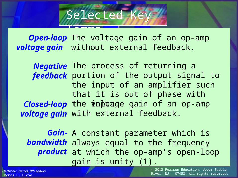
Selected Key TermsSelected Key Terms
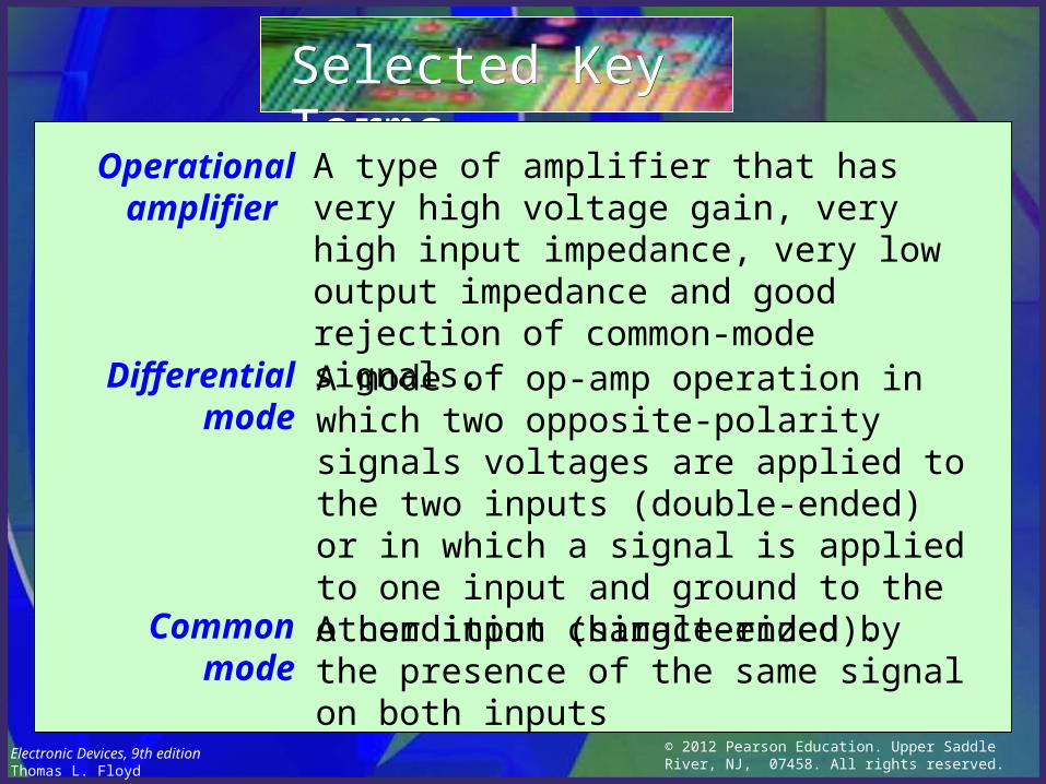
Operational amplifier
Differential mode
Common mode
A type of amplifier that has very high voltage gain, very high input impedance, very low output impedance and good rejection of common-mode signals.
A mode of op-amp operation in which two opposite-polarity signals voltages are applied to the two inputs (double-ended) or in which a signal is applied to one input and ground to the other input (single-ended).
A condition characterized by the presence of the same signal on both inputs
© 2012 Pearson Education. Upper Saddle River, NJ, 07458. All rights reserved.
Electronic Devices, 9th editionThomas L. Floyd
Selected Key TermsSelected Key Terms
Open-loop voltage gain
Negative feedback
Closed-loop voltage gain
Gain-bandwidth
product
The voltage gain of an op-amp without external feedback.
The process of returning a portion of the output signal to the input of an amplifier such that it is out of phase with the input.
The voltage gain of an op-amp with external feedback.
A constant parameter which is always equal to the frequency at which the op-amp’s open-loop gain is unity (1).
© 2012 Pearson Education. Upper Saddle River, NJ, 07458. All rights reserved.
Electronic Devices, 9th editionThomas L. Floyd
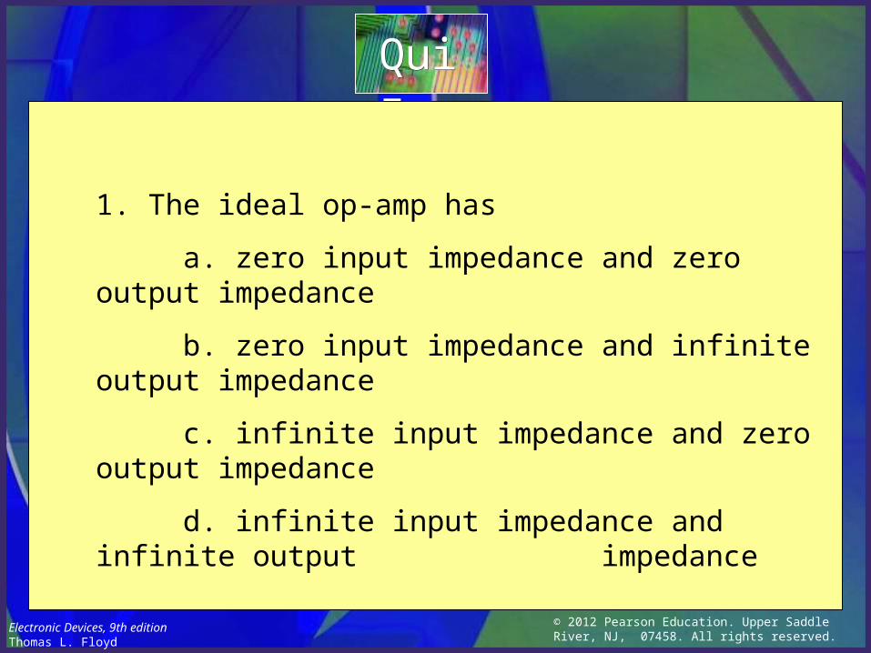
QuizQuiz
1. The ideal op-amp has
a. zero input impedance and zero output impedance
b. zero input impedance and infinite output impedance
c. infinite input impedance and zero output impedance
d. infinite input impedance and infinite output impedance
© 2012 Pearson Education. Upper Saddle River, NJ, 07458. All rights reserved.
Electronic Devices, 9th editionThomas L. Floyd
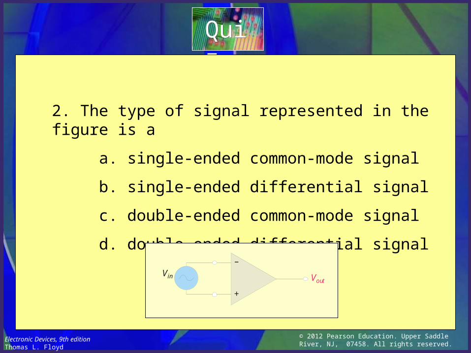
QuizQuiz
2. The type of signal represented in the figure is a
a. single-ended common-mode signal
b. single-ended differential signal
c. double-ended common-mode signal
d. double-ended differential signal
Vin
–
+
Vout
© 2012 Pearson Education. Upper Saddle River, NJ, 07458. All rights reserved.
Electronic Devices, 9th editionThomas L. Floyd
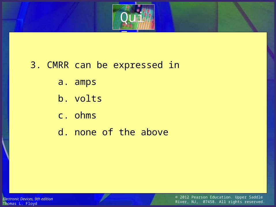
QuizQuiz
3. CMRR can be expressed in
a. amps
b. volts
c. ohms
d. none of the above
© 2012 Pearson Education. Upper Saddle River, NJ, 07458. All rights reserved.
Electronic Devices, 9th editionThomas L. Floyd
QuizQuiz
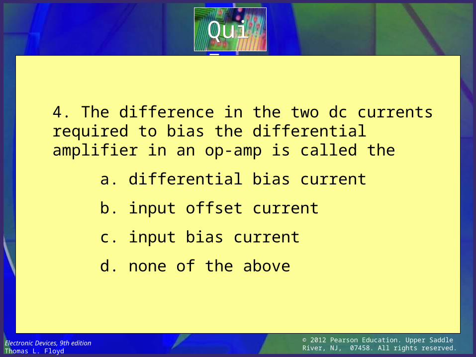
4. The difference in the two dc currents required to bias the differential amplifier in an op-amp is called the
a. differential bias current
b. input offset current
c. input bias current
d. none of the above
© 2012 Pearson Education. Upper Saddle River, NJ, 07458. All rights reserved.
Electronic Devices, 9th editionThomas L. Floyd
QuizQuiz
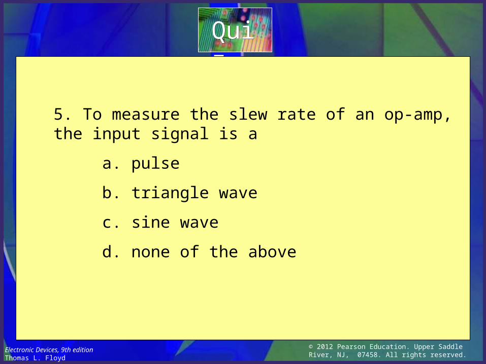
5. To measure the slew rate of an op-amp, the input signal is a
a. pulse
b. triangle wave
c. sine wave
d. none of the above
© 2012 Pearson Education. Upper Saddle River, NJ, 07458. All rights reserved.
Electronic Devices, 9th editionThomas L. Floyd
QuizQuiz
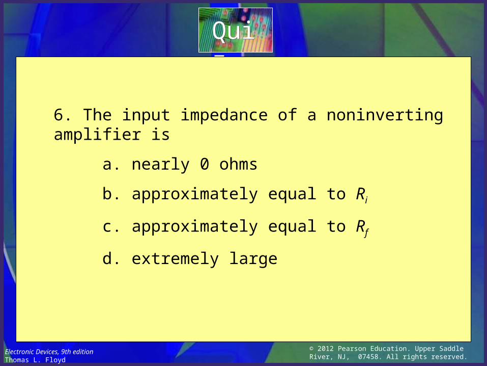
6. The input impedance of a noninverting amplifier is
a. nearly 0 ohms
b. approximately equal to Ri
c. approximately equal to Rf
d. extremely large
© 2012 Pearson Education. Upper Saddle River, NJ, 07458. All rights reserved.
Electronic Devices, 9th editionThomas L. Floyd
QuizQuiz
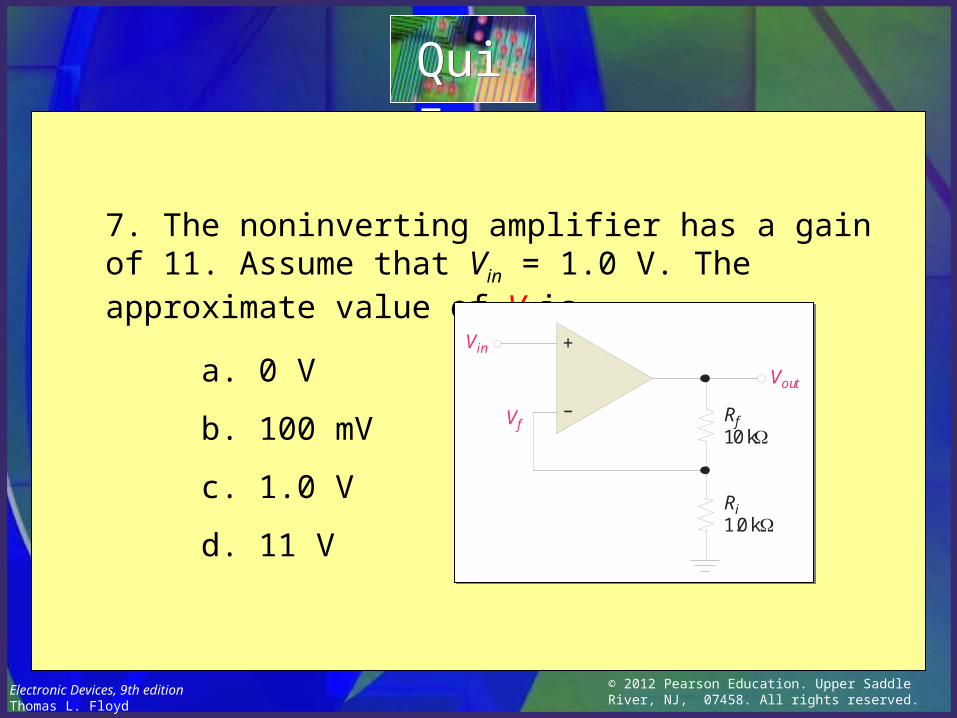
7. The noninverting amplifier has a gain of 11. Assume that Vin = 1.0 V. The approximate value of Vf is
a. 0 V
b. 100 mV
c. 1.0 V
d. 11 V
Rf10 kW
V
V
in
f
+
–
Vout
Ri1.0 kW
© 2012 Pearson Education. Upper Saddle River, NJ, 07458. All rights reserved.
Electronic Devices, 9th editionThomas L. Floyd
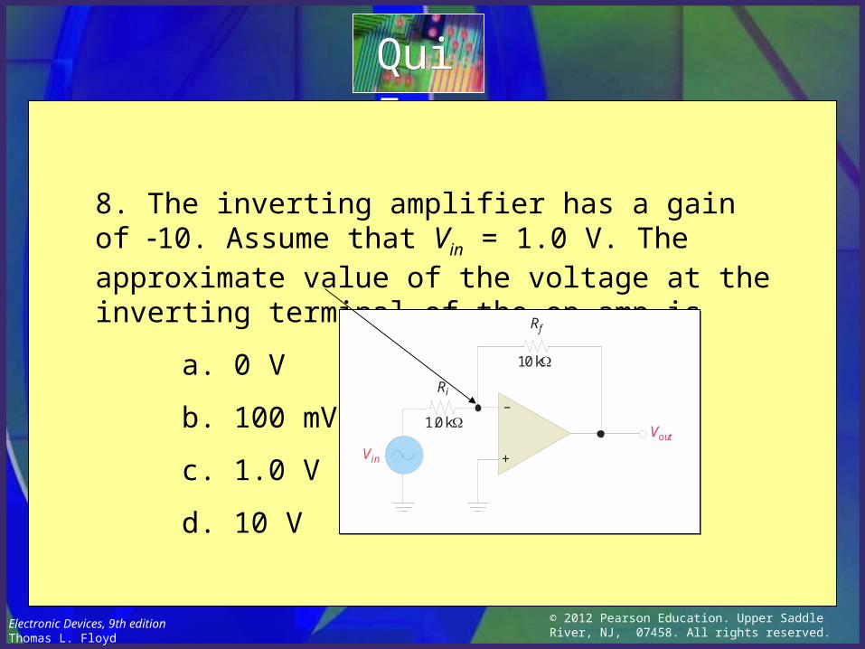
QuizQuiz
8. The inverting amplifier has a gain of 10. Assume that Vin = 1.0 V. The approximate value of the voltage at the inverting terminal of the op-amp is
a. 0 V
b. 100 mV
c. 1.0 V
d. 10 V
–
+
Rf
Vout
Ri
Vin
1.0 kW
10 kW
© 2012 Pearson Education. Upper Saddle River, NJ, 07458. All rights reserved.
Electronic Devices, 9th editionThomas L. Floyd
QuizQuiz
9. To compensate for bias current, the value of Rc should be equal to
a. Ri
b. Rf
c. Ri||Rf
d. Ri + Rf
–
+
Rf
Vout
Ri
Vin
Rc
© 2012 Pearson Education. Upper Saddle River, NJ, 07458. All rights reserved.
Electronic Devices, 9th editionThomas L. Floyd
QuizQuiz
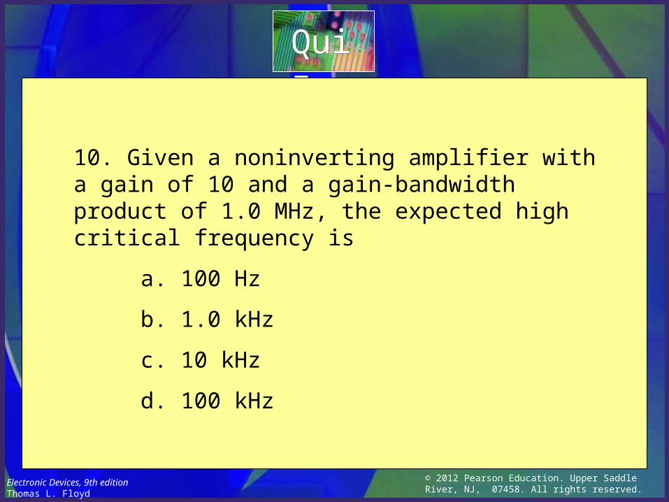
10. Given a noninverting amplifier with a gain of 10 and a gain-bandwidth product of 1.0 MHz, the expected high critical frequency is
a. 100 Hz
b. 1.0 kHz
c. 10 kHz
d. 100 kHz
© 2012 Pearson Education. Upper Saddle River, NJ, 07458. All rights reserved.
Electronic Devices, 9th editionThomas L. Floyd
QuizQuiz
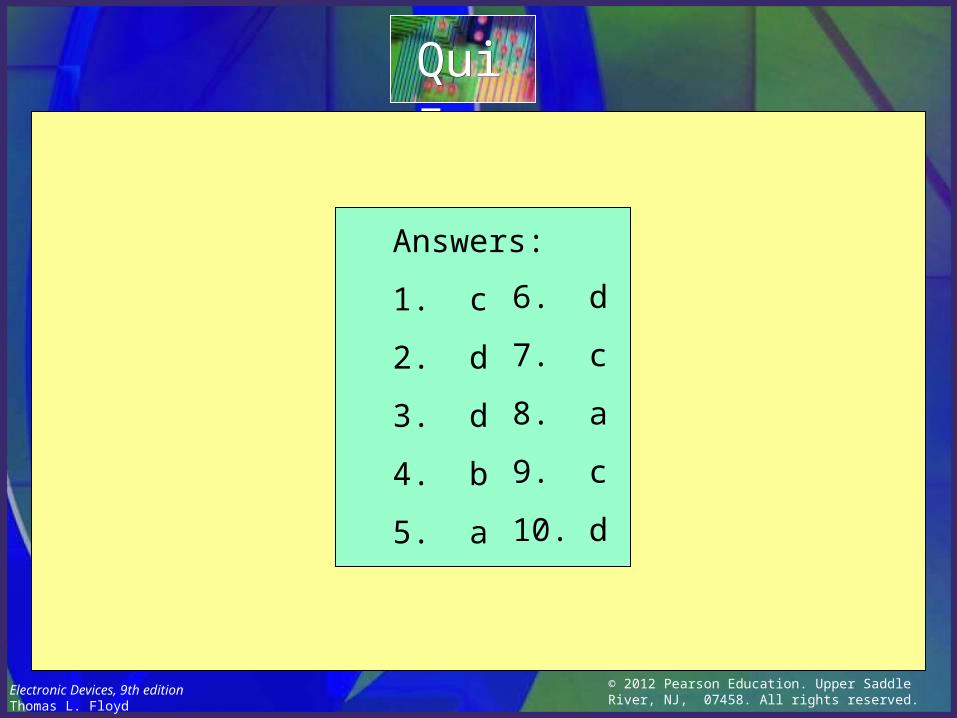
Answers:
1. c
2. d
3. d
4. b
5. a
6. d
7. c
8. a
9. c
10. d


![Electronic devices and circuit theory, 9th ed boylestad[piyali]](https://static.fdocuments.us/doc/165x107/568c4b191a28ab49169ada51/electronic-devices-and-circuit-theory-9th-ed-boylestadpiyali.jpg)