Electron Energy-Loss Spectroscopy and Nanoanalysis (TEM-EELS)
51
Electron Energy-Loss Spectroscopy and Nanoanalysis (TEM-EELS) R.F. Egerton, University of Alberta, Canada ([email protected]) 1. Introduction Electron energy-loss spectroscopy (EELS) involves measurement of the energy distribution of electrons that have interacted with a specimen and lost energy due to inelastic scattering. If the incident electrons have a kinetic energy of a few hundred eV and are reflected from the surface of the specimen, the technique is called high-resolution EELS (HREELS). Relatively simple instrumentation can then provide spectra with an energy resolution down to a few meV, sufficient to resolve vibrational as well as electronic modes of energy loss; this technique is used extensively for studying the physics and chemistry of solid surfaces (Ibach and Mills, 1982; Kesmodel, 2006). The present article is not about HREELS but about spectroscopy employing higher-energy electrons, typically 50 - 300 keV, as used in a transmission electron microscope (TEM). Because of their greater energy, such electrons pass completely through a specimen, provided its thickness is below about 1 μm. The electromagnetic lenses of the TEM can be used to focus them into a “probe” of very small diameter (1 nm or even 0.1 nm) or to produce a transmitted-electron image of the specimen, with a spatial resolution down to atomic dimensions. As a result, EELS carried out in a TEM (TEM-EELS) is capable of very high spatial resolution. Combined with the low specimen thickness, this implies spectroscopic analysis of extremely small volumes of material. For comparison, x-ray absorption spectroscopy (XAS) currently has a lateral resolution of around 30 nm if carried out using synchrotron radiation focused by a zone plate. Owing to the weaker interaction of photons with matter, XAS uses a thicker specimen, which is sometimes an advantage since it allows easier specimen preparation. Also, XAS can examine a specimen surrounded by air or water vapor, whereas the TEM usually places the specimen in a high vacuum. Much of the spectral information obtainable from EELS is similar to that given by synchrotron-XAS, so the TEM-EELS combination has been referred to as a synchrotron in a microscope (Brown, 1997). Because EELS is combined with transmission imaging, electron diffraction and x-ray emission spectroscopy, all in the same instrument, the technique has become important for studying the physics and chemistry of materials. Figure 1a shows a typical energy-loss spectrum, recorded up to a few tens of eV, sometimes called the low-loss region. The first peak, the most intense for a very thin specimen, occurs at 0 eV and is therefore called the zero-loss peak. It represents electrons that did not undergo inelastic scattering (interaction with the electrons of the specimen) but which might have been scattered elastically (through interaction with atomic nuclei) with an energy loss too small to measure. The width of the zero-loss peak, typically 0.2 eV to 2 eV, reflects mainly the energy distribution provided by the electron source.
Transcript of Electron Energy-Loss Spectroscopy and Nanoanalysis (TEM-EELS)

Electron Energy-Loss Spectroscopy and Nanoanalysis (TEM-EELS) R.F. Egerton, University of Alberta, Canada ([email protected]) 1. Introduction Electron energy-loss spectroscopy (EELS) involves measurement of the energy distribution of electrons that have interacted with a specimen and lost energy due to inelastic scattering. If the incident electrons have a kinetic energy of a few hundred eV and are reflected from the surface of the specimen, the technique is called high-resolution EELS (HREELS). Relatively simple instrumentation can then provide spectra with an energy resolution down to a few meV, sufficient to resolve vibrational as well as electronic modes of energy loss; this technique is used extensively for studying the physics and chemistry of solid surfaces (Ibach and Mills, 1982; Kesmodel, 2006).
The present article is not about HREELS but about spectroscopy employing higher-energy electrons, typically 50 - 300 keV, as used in a transmission electron microscope (TEM). Because of their greater energy, such electrons pass completely through a specimen, provided its thickness is below about 1 μm. The electromagnetic lenses of the TEM can be used to focus them into a “probe” of very small diameter (1 nm or even 0.1 nm) or to produce a transmitted-electron image of the specimen, with a spatial resolution down to atomic dimensions. As a result, EELS carried out in a TEM (TEM-EELS) is capable of very high spatial resolution. Combined with the low specimen thickness, this implies spectroscopic analysis of extremely small volumes of material.
For comparison, x-ray absorption spectroscopy (XAS) currently has a lateral
resolution of around 30 nm if carried out using synchrotron radiation focused by a zone plate. Owing to the weaker interaction of photons with matter, XAS uses a thicker specimen, which is sometimes an advantage since it allows easier specimen preparation. Also, XAS can examine a specimen surrounded by air or water vapor, whereas the TEM usually places the specimen in a high vacuum.
Much of the spectral information obtainable from EELS is similar to that given by
synchrotron-XAS, so the TEM-EELS combination has been referred to as a synchrotron in a microscope (Brown, 1997). Because EELS is combined with transmission imaging, electron diffraction and x-ray emission spectroscopy, all in the same instrument, the technique has become important for studying the physics and chemistry of materials.
Figure 1a shows a typical energy-loss spectrum, recorded up to a few tens of eV, sometimes called the low-loss region. The first peak, the most intense for a very thin specimen, occurs at 0 eV and is therefore called the zero-loss peak. It represents electrons that did not undergo inelastic scattering (interaction with the electrons of the specimen) but which might have been scattered elastically (through interaction with atomic nuclei) with an energy loss too small to measure. The width of the zero-loss peak, typically 0.2 eV to 2 eV, reflects mainly the energy distribution provided by the electron source.

Fig.1. Energy-loss spectrum of an iron fluoride film: (a) low-loss region with a logarithmic intensity scale, and (b) part of the core-loss region, with linear vertical scale. Courtesy of Feng Wang, National Institute for Nanotechnology, Edmonton, Canada.
Other low-loss features arise from inelastic scattering by conduction or valence electrons. The most prominent peak, centered around 22 eV in Fig.1a, results from a plasma resonance of the valence electrons. The increase in intensity around 54 eV represents inelastic scattering from inner-shell electrons, in this case the M2 and M3 subshells (3p1/2 and 3p3/2 electrons) of iron atoms. Its characteristic shape, a rapid rise followed by a more gradual fall, is termed an ionization edge; it is the exact equivalent of an absorption edge in XAS. Other ionization edges occur at higher energy loss in Fig.1b: a fluorine K-edge (excitation of 1s electrons) followed by iron L3 and L2 edges (representing excitation of Fe 2p1/2 and 2p3/2 electrons). Before discussing how these various features provide us with information about the specimen, we briefly examine the principles and instrumentation involved in obtaining energy-loss spectra in the TEM. 2. Instrumentation TEM-EELS instrumentation is based on the magnetic-prism spectrometer, in which a uniform magnetic field B (of the order of 0.01 T) is generated by an electromagnet with carefully shaped polepieces; see Fig. 2. Within this field, electrons follow circular paths of radius R and are deflected through an angle of typically 90°. The sideways force on an electron is F = Bev = mv2/R, where e, v and γm0 are the electron speed, charge and relativistic mass, giving a bend radius that depends on speed and therefore on electron energy:
R = γm0(eB)-1 v (1) While this behavior resembles the bending and dispersion of a beam of white light by a glass prism, the electron prism also has a focusing action. Electrons that stray from the central trajectory (the optic axis) in a direction perpendicular to the field (Fig. 2a) experience an increase or decrease in their path length within the field, giving rise to a

greater or lesser deflection angle. If the entrance beam originates from a point object, electrons of a given energy are returned to a single image point. The existence of different electron energies then results in a focused spectrum in a plane passing through that point. In addition, the fringing field at the polepiece edges focuses electrons that deviate in the y-direction, parallel to the magnetic field (Fig. 2b). By adjusting the angles of the polepiece edges, the focusing power in these two perpendicular directions can be made equal (double-focusing condition), giving a spectrum of small width in the y-direction. As a result of second-order aberrations, the focusing is imperfect but these aberrations can be corrected by curving the polepiece edges or by incorporating multipole lenses, allowing an energy resolution better than 1 eV for an entrance angle γ of up to several milliradians (of the order of 0.1º).
Fig. 2. Dispersive and focusing properties of a magnetic prism (a) in the x-z plane, perpendicular to the magnetic field, and (b) in the y-direction, parallel to the field. Solid lines represent zero-loss electrons (E = 0); dashed lines represent electrons that have lost energy during transmission through the specimen.
The simplest form of energy-loss system consists of a conventional TEM fitted with a magnetic prism below its image-viewing chamber (Fig. 3a). By tilting the TEM screen to a vertical position, electrons are allowed to enter the spectrometer, where they are dispersed according to their kinetic energy, i.e. their incident energy E0 minus any energy loss E incurred in the specimen. The spectrometer object point is an electron-beam crossover produced just below the bore of the final (projector) TEM lens. A spectrometer entrance aperture, typically variable from 1 to 5 mm in diameter, limits the range of entrance angles and ensures adequate energy resolution. This kind of system requires little or no modification of the TEM, which operates according to its original design and specification.

An alternative strategy is to incorporate a spectrometer into the TEM column (Fig. 3b). For mechanical stability, it is important to preserve a vertical TEM column, so there are usually four magnetic prisms that bend the beam into the shape of a Greek letter Ω, hence the name “omega filter”. An energy-loss spectrum is produced just below the filter and subsequent TEM lenses project it onto the viewing screen or onto an electronic detector, usually employing a CCD camera. Alternatively, these lenses can focus a plane (within the spectrometer) that contains an image of the specimen, utilizing the imaging properties of a magnetic prism. If a narrow slit is inserted at the spectrum plane, all electrons are removed except those within a small energy window, resulting in an energy-filtered (EFTEM) image at the TEM screen or CCD camera. Provided its image aberrations are corrected by quadrupole and sextupole lenses, the post-column magnetic prism (Fig. 3a) can also produce EFTEM images, as in the GIF spectrometer marketed by the Gatan Company.
A third type of system (Fig. 3c) is based on the scanning–transmission electron
microscope (STEM), in which a field-emission source and strong electromagnetic lenses are used to form a small probe that can be raster-scanned across the specimen. A dark-field image, representing transmitted electrons scattered through relatively large angles, is formed by feeding the signal from a ring-shaped (annular) detector to a display device scanned in synchronism with the probe scan. Electrons scattered through smaller angles enter a single-prism spectrometer, which produces an energy-loss spectrum for a given position of the probe on the specimen (Browning et al., 1997). Inserting a slit in the spectrum plane then gives an energy-filtered image, obtained this time in serial mode. Alternatively, the whole spectrum is read out at each probe position (pixel), resulting in a large spectrum-image data set that can be processed off-line (Jeanguillaume and Colliex, 1989). Similar data is obtainedable from an EFTEM system (Fig.3b) by recording a sequence of EFTEM images of different energy loss, selected by changing the spectrometer current or the microscope high voltage.
Energy-loss spectra were once recorded photographically but this arrangement soon gave way to electronic acquisition. In a serial-recording system, a narrow slit is placed in the spectrum plane and the spectrum scanned past the slit by varying the magnetic field of the prism or the microscope high voltage; raising the voltage selects a higher energy loss, for a given slit position. A single-channel electron detector behind the slit produces an electrical signal proportional to the electron intensity at each energy loss; it usually consists of a scintillator, to convert the electrons to visible photons, and a photomultiplier tube that acts as a high-sensitivity photon detector. This simple system works well but provides noisy data at high energy loss, where the electron intensity is weak. The reason lies not in the photomultiplier tube, which is a low-noise detector, but in the fact that only a small range of energy loss is sampled at any instant, resulting in pronounced shot noise due to the limited number of electrons being recorded.

Fig. 3. Three procedures for TEM-based energy-loss spectroscopy: (a) conventional TEM with a magnetic-prism spectrometer below the viewing screen, (b) TEM incorporating an in-column imaging filter, and (c) scanning–transmission (STEM) system.
To facilitate recording higher energy losses, parallel-recording detectors were developed, with no energy-selecting slit so that no electrons are wasted. An extended range of the energy-loss spectrum is projected by an electron lens onto a fluorescent screen, coupled to a CCD camera whose output is fed into the data-recording computer. Although this procedure has largely replaced serial recording, it gives spectral peaks with extended tails that arise from light scattering in the fluorescent screen. These tails can be removed by spectrum processing (deconvolution) or minimized by using a high spectral dispersion (although this limits the energy range of the data).
The energy resolution of an energy-loss spectrum is determined by several factors, including aberrations of the electron spectrometer. By curving the polepieces of the magnetic prism and by using weak multipole lenses for fine tuning, these aberrations can be almost eliminated. The energy resolution is then determined by the width of the energy distribution provided by the electron source, seen as the width of the zero-loss peak. Thermionic sources, such as the tungsten filament or heated LaB6 source used in many electron microscopes, provide an energy width between 1eV and 2 eV. A Schottky source (heated Zr-coated W tip) gives a width of about 0.7 eV. A CFEG source (field-emission from a cold tungsten tip) gives typically 0.5 eV, although fast readout of the spectrum combined with software re-alignment can reduce this width to below 0.3 eV (Kimoto and Matsui, 2002; Nelayah et al., 2007).

Further improvement in energy resolution is possible by inserting an electron
monochromator after the electron source. The monochromator is an energy filter tuned to a narrow energy band at the centre of the emitted-energy distribution. Both magnetic-prism and electrostatic-prism designs are possible but a popular choice is the Wien filter, which uses both electric and magnetic fields and provides an energy width of about 0.2 eV (Tiemeijer, 1999). Another recent development is the correction of TEM-lens aberrations by multipole lenses that are adjusted and aligned under computer control. Used to correct the spherical aberration of a probe-forming lens (e.g. the objective lens of a STEM), the corrector allows electrons to be focused into a probe of diameter below 0.1 nm (Krivanek et al., 1999). Similar techniques can be used to correct the spherical and chromatic aberration of the first imaging lens (objective) of a conventional TEM (Haider et al., 1998). Although subatomic resolution might seem unnecessary, it greatly assists the atomic-scale analysis of individual defects in crystalline materials. 3. The Physics of EELS When electrons pass through a specimen, they are scattered (changed in direction) by interaction with atoms of the solid. This interaction (or collision) involves electrostatic (Coulomb) forces, arising from the fact that the incident electron and the components of an atom (nucleus and atomic electrons) are all charged particles. For convenience we can divide the scattering into elastic and inelastic, depending on whether or not the incident electron responds to the field of the nucleus or to its surrounding electrons. 3.1 Elastic Scattering Elastic scattering involves the interaction of an incident electron with an atomic nucleus. Because the nuclear mass greatly exceeds the rest mass of an electron (by a factor 1840A, where A = atomic weight or mass number), the energy exchange is small and usually unmeasurable in a TEM-EELS system. For elastic scattering by a single atom (and in an amorphous material, to a first approximation) the differential cross section that represents the probability of scattering per unit solid angle Ω is (Lenz, 1954):
dσe/dΩ = [4Z2/(k0
2T)] (θ2 +θ02)-2 (2)
Here Z is atomic number, k0 is the electron wavenumber (2π/wavelength) and T is an “effective” incident energy given by:
T = m0v02/2 = E0[1+E0/(2m0c2)]/[1+E0/(m0c2) ] (3)
where m0c2 = 511 keV is the electron rest energy. The parameter T is somewhat less than the actual kinetic energy E0 because the relativistic mass of the electron exceeds its rest mass m0; see Table 1. In Eq.(2), θ represents scattering angle of the electron and θ0 ≈ Z1/3/(k0a0) is the angular width of the scattering distribution, a0 being the first Bohr radius

(53×10-12m). For Z = 6 and E0 = 100 keV, θ0 ≈ 20mrad ≈ 0.35deg, meaning that the angular distribution of elastic scattering is quite narrow for the incident-electron energies used in a TEM; see Fig.4. To be scattered through a large angle (θ >> θ0), the electron must pass very close to the nucleus; and Eq.(2) approximates to the Rutherford formula for scattering of an electron from an unscreened nucleus. At smaller angles, the scattered intensity falls below the Rutherford value, the term θ0 representing nuclear screening by the atomic electrons.
E0(keV) T (keV) γT (keV) γ λ (pm) k0 (nm-1) 30 27.6 29.2 1.059 6.98 900
100 76.8 91.8 1.196 3.70 1697 200 123.6 171.9 1.391 2.51 2505 300 154.1 244.5 1.587 1.97 3191
1000 226.3 669 2.957 0.87 7205
Table 1. Parameters T = m0v2/2, γT, γ = m/m0, deBroglie wavelength λ and wavenumber k0 = 2π/λ, as a function of the kinetic energy E0 of an electron.
A crystalline specimen scatters electrons over a similar angular range but the
scattering is peaked at discrete angles (each twice a Bragg angle; see Fig.4) and the elastic scattering is then called diffraction. Because of atomic vibration, electrons can also undergo phonon scattering, which transfers intensity from Bragg beams into the intervening background and involves energy transfers of the order of kT ( ≈ 25 meV at T ≈ 300 K) that are unmeasurable in a TEM-EELS system. For this reason and the fact that it involves interaction with atomic nuclei, phonon scattering is often termed quasi-elastic.
Fig. 4. Curves show the angular distribution of elastic and inelastic scattering, calculated for 200keV electrons in amorphous carbon. Vertical bars represent the relative intensities of the elastic Bragg beams in crystalline diamond when its crystal axes are parallel to the incident beam.

For the small fraction of incident electrons that are scattered through large angles, elastic scattering does result in an appreciable energy transfer E given by:
E = Emax sin2(θ/2) (4) For the extreme case of 180° backscattering, E = Emax ≈ E0 / (457A) ≈ 18 eV for a carbon atom and E0 =100 keV. If E0 is several hundred keV, this “elastic” scattering can be sufficient to displace an atom from its lattice site in a crystal or eject surface atoms into the vacuum, giving rise to a form of radiation damage called knock-on or displacement damage. 3.2 Inelastic Scattering Coulomb interaction between the incident electron and atomic electrons gives rise to inelastic scattering. Because the projectile (incident electron) and the target (atomic electron) have similar mass, the energy exchange (loss) can be appreciable: typically a few eV up to hundreds of eV. For most inelastic collisions, the double-differential cross section is given by a small-angle approximation:
d2σi/dΩdE = (4γ2/k02)(R/E) (df/dE) = (4a0
2R2/T) [(1/E)(df/dE)] (θ2 +θE2)-1 (5)
where q is the magnitude of the scattering wavevector, a0
= 53×10-12 m, R = 13.6eV (the Rydberg energy) and df/dE is an energy-differential optical oscillator strength, a function of energy loss E but not of scattering angle θ. As seen from Eq.(5), the angular distribution of inelastic scattering is a Lorentzian function whose half-width (at half-height) is the characteristic angle θE = E/(2γT). Although the relativistic factor γ (the fractional increase in relativistic mass of the incident electron) is greater than 1, the term γT is slightly less than the kinetic energy E0 of the incident electrons, as seen in Table 1. For an energy loss of E = 25 eV, θE = 0.14 mrad, showing that inelastic scattering involves angles even smaller than those for elastic scattering; see Fig. 4.
Apart from the 1/E and angular terms in Eq.(5), which taken together imply a
monotonic decay (E-1 for large θ, E-3 for very small θ), df/dE represents the energy dependence of inelastic scattering. This energy-differential oscillator strength applies also to photon-induced transitions, indicating the close connection between energy-loss and optical spectra. This correspondence is only approximate: when a photon is absorbed, the momentum transfer corresponds to a wavenumber Kp = ω/c = 2πE/(hc), E being the transferred energy. The momentum hKq/(2π) transferred by an inelastically scattered electron depends on its scattering angle; energy and momentum conservation lead to:
K2= k0
2(θ2 +θE2) (6)
The minimum momentum transfer corresponds to θ = 0 and Kmin= k0θE, so for the same energy transfer :
Kmin/Kp = (2πγm0v/h)[E/(2γT)][hc/(2πE)] = c/v (7)

Provided the incident-electron energy is at least 100 keV (v/c ≈ 0.55) and the energy-loss spectrum is recorded using a very small angle-limiting spectrometer-entrance aperture (β<< θE), the transferred momentum is only a factor of two larger than for photon absorption. The energy-loss spectrum then represents optical (direct) electronic transitions that obey a dipole sum rule: the angular-momentum quantum number l of the target atom must increase or decrease by one (Δl = ±1).
The E-dependence df/dE is characteristic of the specimen, hence the usefulness of
EELS. We now discuss some of the mechanisms that give rise to this energy dependence. 3.3 Plasmon excitation. A prominent form of inelastic scattering in solids involves plasmon excitation. This phenomenon arises from the fact that outer-shell electrons (conduction electrons in a metal, valence electrons in a semiconductor or insulator) are only weakly bound to atomic nuclei and are coupled to each other by electrostatic forces; their quantum states are delocalized in the form of an energy band.
When a fast-moving electron passes through a solid, the nearby atomic electrons are displaced by Coulomb repulsion, forming a correlation hole (a region of net positive potential of size ~ 1 nm) that trails behind the electron. Provided the electron speed exceeds the Fermi velocity, the response of the atomic electrons is oscillatory, resulting in regions of alternating positive and negative space charge along the electron trajectory; see Fig. 5. This effect is known as a plasmon wake, by analogy with the wake of a boat traveling on water at a speed higher than the wave velocity, or an aircraft flying faster than the speed of sound. The wake periodicity in the direction of the electron trajectory is λw = v/fp where fp is a plasma frequency given (in Hz) by
2π fp = ωp = [ne2/(ε0 m)]1/2 (8) Here n is the density of the outer-shell (conduction or valence) electrons and m is their effective mass. The frequency fp is of the order of 1016 Hz, equivalent to the ultraviolet region of the electromagnetic spectrum.
Fig. 5. Plasmon wake of a 100keV electron traveling through aluminum, calculated from dielectric properties (P.E. Batson, personal communication). The electron is represented by the bright dot on the left; alternate dark and bright bands represent positive and negative regions of space charge that trail behind the electron.

As the electron moves through the solid, the backward attractive force of the positive correlation hole results in energy loss. The process can be viewed in terms of the creation of pseudoparticles known as plasmons, each of which carries a quantum of energy equal to Ep = hfp = (h/2π)ωp. The inelastic scattering is then interpreted as the creation of a plasmon at each scattering “event” of the transmitted electron, resulting in an energy-loss spectrum containing peaks at an energy loss E = Ep and multiples of that energy; see Fig.6.
Fig. 6. Energy-loss spectrum recorded from a thin region of silicon (thin line) and from a thicker area (thick line), with their zero-loss peaks matched in height. Plasmon peaks occur at multiples of the plasmon energy (Ep = 16.7 eV). The broad feature starting around 100 eV is a silicon L23 ionization edge.
The probability Pn of n plasmon-loss events in a specimen of thickness t is given by Poisson statistics:
Pn = (1/n!)(t/λi)n exp(-t/λi) (9) where the plasmon mean free path λi is an average distance between scattering events. The integrated intensity In of each plasmon peak is then given by:
In = Pn It = (1/n!)(t/λi)n exp(-t/λi) It = (1/n!)(t/λi)n I0 (10) where It is the total integral of the spectrum, including its zero-loss component I0. In the absence of elastic scattering, It would be the incident-beam intensity; in practice it represents electrons that, after transmission through the specimen, are scattered through angles small enough to be accepted by the spectrometer entrance aperture (semiangle β).
The spectrometer entrance aperture also cuts off some inelastic scattering (less than the elastic because of the narrower angular distribution), reducing the inelastic intensity from In to In(β). As a result of a fortuitous property of the Lorentzian angular distribution, In(β)/In = [I1(β)/I1]n to a good approximation, which allows Eq.(10) to be used in the presence of an angle-limiting aperture so long as λi is replaced by a value

λi(β) that depends (logarithmically) on the spectrometer collection angle β (Egerton, 2011).
Based on Eq. (10), the plural-scattering component of an energy-loss spectrum
can be removed by Fourier-log deconvolution (Johnson and Spence, l974). Because of the property just discussed, this procedure is accurate even for spectra recorded with an angle-limiting aperture, provided the aperture is centred on the optic axis (θ = 0). For spectra recorded off-axis (large q), more complicated procedures are necessary.
Since inelastic scattering is caused by the electric field of the incident electron, similar effects are created by an electromagnetic wave. As a result, the energy-loss spectrum is related to the dielectric properties of the specimen. In fact, the middle term (1/E)(df/dE) in Eq.(5) can be replaced by Im[-1/ε(E)] = ε2/(ε1
2+ε22), known as the energy-
loss function, where ε(E) is a complex permittivity whose real and imaginary parts are ε1
and ε2. As a result of this connection, energy-loss spectra can be processed to give ε1(E) and ε2(E) data over a wide range of photon energy E, ranging from the visible to the x-ray region. The processing involves Kramers-Kronig transformation to get Re(1/ε) and various normalisation procedures (Egerton, 2011; Alexander et al., 2008).
The dielectric formalism allows energy-loss spectra to be simulated. In the simple
Drude model (Raether, 1980), the outer-shell atomic electrons are approximated by a Fermi sea of free electrons (jellium) for which the complex permittivity is
ε = 1 – Ep
2/(E2 + iE Γ) = 1 - Ep2/(E2 + Γ2) + i ΓEp
2 / [E(E2 + Γ2)] (11)
The energy-loss function is then:
Im[-1/ε(E)] = E Γ Ep2 / [(E2 – Ep
2)2 + (E Γ)2] (12)
Fig.7. Permittivity and energy-loss function calculated from the Drude model for (a) a free-electron gas with Ep = 15 eV, Γ = 1.5 eV (typical of aluminum recorded by a TEM-EELS system), and (b) Ep = 21 eV, Eb = 14 eV, Γ = 20 eV, which gives an energy-loss function representative of amorphous Al2O3.

The parameter Γ represents plasmon damping and is approximately the full width at half maximum (FWHM) of the plasmon peak in the energy-loss spectrum. Equation (12) describes the shape of this peak; see Fig.7a. Note that for the free-electron case, the resonance peak occurs when ε1(E) is close to zero; at this energy, there is no peak in ε2(E) that would give rise to a peak in the optical-absorption spectrum
Except for the transition elements, whose d-electrons are not entirely free to take place in collective motion, the free-electron approximation: Eq.(8) with m = m0, gives plasmon-peak energies quite close to those measured by EELS; see Fig.8. This fact remains true even for semiconductors such as silicon and insulators such as diamond or alkali halides; see Table 2. To take part in plasmon oscillation, the outer-shell electrons need not be capable of long-range motion (electrical conduction).
The Drude model can be extended to semiconductors and insulators by giving the
electrons a binding energy Eb, resulting in a permittivity: ε = 1 − Ep
2/(E2 − Eb2 + iEΓ)
= 1 − Ep2(E2−Eb
2)/[(E2−Eb2)2+ E2Γ2] + i EΓEp
2 /[(E2–Eb2)2 + E2 Γ2] (13)
resulting in a plasmon peak displaced to an energy slightly higher than Ep, as illustrated for amorphous Al2O3 in Fig.7b. Note that the broad plasmon resonance now occurs at ε1 ≈ ε2 , with ε1 never becoming zero or negative.
Fig.8. Plasmon energy (in eV) for elements, as measured (solid circles) and as given by the free-electron formula (open circles). Agreement is good except for the transition metals (22 < Z < 29), where the d-electrons contribute to an M23 ionization edge at higher energy loss (35eV to 60eV) rather than to the plasmon peak.

Mater
ial Ep(eV)
measured Ep(eV)
free-electron hΓ/2π (eV) = FWHM
θc(mrad) E0 = 100keV
λp(θc) in nm E0 = 100keV
Al 15.0 15.8 0.5 7.7 119 Be 18.7 18.4 4.8 7.1 102 Si 16.7 16.6 3.2 6.5 115
GaAs 15.9 15.7 5.5 MgO 22.3 24.3 6.7 NaCl 15.5 15.7 15
Table 2. Measured and calculated plasmon energy, plasmon-peak width (FWHM), cutoff angle θc(mrad) and mean free path λp(θc) for E0 = 100 keV.
As shown in Table 2, the plasmon peak indicates a sharp resonance in some
materials, including Al, alkali metals and some semiconductors such as silicon and GaAs. Other materials, such as carbon and organic compounds, show broad plasmon peaks; the peak width hΓ/(2π) is large because of strong plasmon damping. Transfer of plasmon energy to individual electrons (single-electron excitation) is one cause of damping and becomes more probable at higher q, so the plasmon-peak width increases with increasing scattering angle. Damping can also increase at very small angles, due to grain-boundary scattering in a polycrystalline material (Krishnan and Ritchie, 1970). The plasmon width is higher in amorphous materials (Egerton, 2011); for example 3.9 eV in amorphous silicon compared to 3.2 eV in the crystalline phase.
An n-type semiconductor has a separate plasma resonance associated with its
conduction-band electrons. However, their concentration is typically below 1019 cm-2, giving a plasmon energy below 0.25 eV, not resolvable by most TEM-EELS systems.
Carbon represents an interesting case. Assuming four valence electrons per atom, diamond has a free-electron plasmon energy of 31 eV. The measured loss spectrum shows a broad peak centered around 33eV and about 13 eV in width, corresponding to a well-damped plasmon resonance. Graphite is a semi-metal with one weakly-bound π-electron per atom, giving free-electron plasmon energy of 12.6 eV as well as a 22eV resonance due to all four electrons. In practice, two resonance peaks are observed, at 7 eV and 27 eV; the resonance frequencies are forced apart due to coupling between the two groups of oscillators (Raether, 1980). For single-sheet graphene, these peaks are red-shifted to 4.7 eV and 14.6 eV (Eberlein et al., 2008).
Organic compounds give a broad low-loss peak, typically centered around 23 eV
but with some fine structure at lower energy loss. In compounds containing double
bonds, a further peak at around 6 eV is sometimes interpreted as a plasmon resonance of π-electrons. However, vapor-phase aromatic hydrocarbons show a similar peak, which must be interpreted in terms of π-π* transitions (Koch and Otto, 1969). A peak in the range 6 – 7 eV is often taken as evidence of double bonds or an aromatic structure. Ice also shows a broad resonance around 20 eV, accompanied by fine structure below 10 eV due to interband transitions (Sun et al., 1993).
Plasmon dispersion means that the plasmon peak shifts to higher energy with
increasing scattering angle (and wavenumber), by an amount proportional to q2. This behaviour is sometimes used to identify a spectral peak as representing a bulk (volume) plasmon, rather than single-electron excitation where the energy is expected to be independent of q.
The free-electron approximation provides a value for the mean free path (MFP)
for plasmon excitation: λp(β) ≈ (4a0T/Ep)[ln(1+β2/θ Ep
2)]-1= 8πa0T e-1h-1 (ε0m0uA/ρ)1/2 z-1[ln(1+β2/θ Ep2)]-1 (14)
where u is the atomic mass unit, ρ is the physical density and z is the number of quasi-free electrons per atom. The natural-logarithm term represents integration of Eq.(5) up to a collection angle β, taking E ≈ Ep such that θEp
= Ep/(2γT). This term causes the MFP to decrease somewhat with increasing collection angle, by about a factor of about 2 between β = 1 mrad and 10 mrad.
In reality, Eq.(14) is a small-angle approximation, valid for scattering angles less than a critical angle θc (known as the dipole region). The wavenumber q associated with inelastic scattering is given by Eq.(6) and increases with scattering angle. When the phase velocity ωp/q of the plasmon wave exceeds the Fermi velocity of the material, energy can be transferred to individual electrons and the plasmon mode becomes very highly damped; the effective oscillator strength df/dE falls rapidly to zero when θ exceeds θc. For β > θc, β should therefore be replaced by θc in Eq.(14), giving a total MFP appropriate to large collection angles.
The plasmon total MFP exhibits a cyclic dependence on atomic number Z due to the cyclic nature of the number z of quasi-free electrons per atom. This behaviour has been confirmed by experiment and the free-electron formula found to give a MFP within a few percent of the experimental values (Iakoubovskii et al., 2008b). 3.4 Surface plasmons and radiation loss Even before a beam electron enters the specimen, its electric charge polarizes the entrance surface. In the case of a conductor, this sets up a longitudinal charge-density wave cos(qx-ωt) whose angular frequency of oscillation ω satisfies a boundary condition at the surface:
εa(ω) + εb(ω) = 0 (15)

where εb(ω) and εa(ω) are relative permittivities of the specimen and its surroundings. The simplest case is an interface between vacuum and a free-electron metal: εa(ω) = 1 and εb(ω) = 1 - ωp
2/ω2. Equation (15) then gives ω = ωs = ωp/√2, indicating that the energy-loss spectrum will include a surface-plasmon peak centred about an energy Es given by
Es = (h/2π)(ωp/√2) = Ep/√2 (16) For an insulator/metal boundary, where the permittivity of the insulator has a positive real part ε1 and both insulator and metal have negligible imaginary parts at frequencies close to ωs, Eq.(15) gives:
Es = Ep/(1 + ε1)1/2 (17) In agreement with experiment (Powell and Swan, 1960), Stern and Ferrell (1960) showed that Eq.(17) applies to an oxidized metal surface provided the oxide layer is thicker than about 3 nm. They also derived an expression for the probability of scattering (per unit solid angle Ω ) of the incident electron as a result of surface-plasmon excitation:
dPs/dΩ = h [π2a0m0v(1+ε1)]-1 θθE (θ2 + θE2)-2 f(θ,θi,ψ) (18)
where θE = E/(γm0v2) = E/(2γT) as previously; θi is the angle between the surface normal and the incident beam; ψ is the angle between the plane of incidence and the detector and f(θ,θi,ψ) = [(1+θE
2/θ2)/cos2(θi) – (tanθi cosψ + θE/θ )2 ]1/2 ≈ 1 for θi < 0.1 rad, θ >>θE . For θi = 0 (normal incidence), f(θ,θi,ψ) = 1 and the scattered-electron intensity is zero at θ = 0, rising to a maximum at θ = θE/√3 and then falling proportional to θ-3 for θ >> θE. Since θE is very small (< 0.1 mrad typically), the surface-plasmon intensity is concentrated into even smaller angles than volume-plasmon scattering, which falls as θ-2 for θ >> θE. Surface-mode contributions to the loss spectrum are therefore minimized by displacing the angle-selecting aperture away from optic axis or by using a collection aperture with a central stop.
Alternatively, if an axial and relatively large collection aperture is used (β>> θE), the total probability of surface-plasmon excitation at a single interface, for normal incidence (θi = 0) and integrated around the Es peak, is (Ritchie, 1957; Stern and Ferrell, 1960):
Ps = h [2a0m0v(1+ε1)]-1 (19)
and is of the order of 1% at each surface for 100-keV incident electrons. This means that surface-plasmon peaks are prominent (relative to bulk-plasmon peaks) only for rather thin specimens (t < 20 nm). There is also a negative contribution (-Ps/2) around the bulk-plasmon energy Ep, arising from the so-called begrenzungs effect (Ritchie, 1957).

As the specimen is tilted away from perpendicular incidence, the angular distribution of surface-plasmon scattering becomes asymmetrical relative to the optic axis (see Fig. 9) and the integrated intensity increases by a factor ≈1/cosθi. For large θi, surface-plasmon scattering dominates over bulk-plasmon peaks, as in the case of surface-reflection spectra where electrons are elastically reflected back into vacuum after penetrating only a short distance into the specimen (Powell, 1968). A similar situation exists when the electrons are focused into a fine probe (sub-nm diameter) positioned within a few nm beyond the edge of a particle. In this aloof mode of spectroscopy, energy losses due to surface plasmons predominate (Howie, 1983; Batson, 2008).
Fig.9. Angular distribution of surface-plasmon scattering within the plane of incidence, for electron beams with various angles of incidence θi relative to the surface-normal.
To predict the energy dependence of surface-loss intensity, we need to know the energy dependence of the permittivities on both sides of the interface. For perpendicular incidence, the interface-loss probability integrated up to an angle β is:
dPs/dE = (πa0k0T)-1 [(1/θE) tan-1(β/θE)] {Im[-4/(εa+εb)] - Im[-1/εa] - Im[-1/εb]} (20) This expression is symmetric with respect to the two media; the direction of travel of the electron does not matter. Negative terms of the form Im(-1/ε) indicate that the interface plasmon intensity occurs at the expense of volume-plasmon intensity (the energy-integrated oscillator strength being unaltered by the interface). This is the begrenzungs effect, which arises because the bulk-plasmon wake requires a distance λp/4=(π/2)(v/ωp) to become established on each side of the interface (Garcia de Abajo and Echenique, 1992; Egerton, 2011). Our previous equations all assume that the thickness t of each material is large enough that there is negligible electrostatic coupling between the surface-plasmon fields at its two surfaces: qst >> 1, where qs = k0θ for perpendicular incidence. Kröger (1968) gave a more complete derivation of the energy-loss intensity for an electron transmitted through a foil of any thickness, including coupling of the plasmon modes between the two surfaces and a relativistic retardation effect related to the generation of Čerenkov radiation. His formula for the energy-loss intensity contains seven terms, of which the

last three vanish for normal incidence (θi = 0). The first term is proportional to specimen thickness and corresponds to bulk losses; other terms represent surface excitations. Several of the terms contain a resonance denominator that becomes zero at a certain energy loss E, corresponding to emission of Čerenkov radiation when the electron speed v is higher than the speed of light: c/ε1(E)1/2 in the specimen. This radiation loss gives rise to peaks (at a few eV loss) that can interfere with bandgap measurements in semiconductors (Stöger-Pollach et al., 2006). In the TEM, the Čerenkov and surface-plasmon contributions can be minimized by using an off-axis collection aperture or an on-axis aperture with a central stop (Stöger-Pollach, 2008). However, these steps are only effective for near-parallel illumination; a highly-focused STEM probe involves incident convergence angles of several mrad.
Erni and Browning (2008) have evaluated the Kröger equations for several semiconductors and an insulator (Si3N4); see Fig.10. Volume retardation leads to a peak in the energy-loss spectrum below 10 eV and a peak in the angular distribution below 0.1 mrad, but when the specimen is thinner than about 300 nm, surface-mode scattering becomes important and results in guided-light modes arising from total internal reflection of the Čerenkov radiation. Above 100nm thickness, the low-loss spectra are dominated by the volume plasmon and Čerenkov peaks, around 10nm by volume and surface plasmons and at very low thickness by surface and guided-light modes. The guided modes have a dispersion lying between the light line for vacuum (ω = cq) and that in the semiconductor (ω = cq/n = cq/ε1
1/2), as explained by Raether (1980).
Fig.10. (a) Schematic and contour plot (grey background) showing the calculated energy-loss and angular dependence of intensity for a 50nm Si specimen with 300keV incident electrons. (b) Calculated energy-loss spectra for 2.1mrad collection semiangle, 300keV incident electrons and various thicknesses of Si, assuming no surface oxide layer. Reproduced from Erni and Browning (2008), copyright Elsevier.

Both Čerenkov and surface-plasmon modes complicate the Kramers-Kronig process of obtaining dielectric data from EELS measurements. Čerenkov effects are particularly severe in the case of insulators such as diamond (Zhang et al., 2008). New Čerenkov modes have been predicted for electrons passing close to small particles (Itskovsky et al., 2008) and new surface-plasmon modes in small particles have been revealed by energy-filtered imaging (Nehayah et al., 2007; Rossouw et al., 2011). This is an active area of research, made possible by recent improvements in energy resolution. 3.5 Single-electron excitation and fine structure In addition to the collective response, a transmitted electron can excite individual atomic electrons to quantum states of higher energy. Evidence for these single-electron excitations is seen in the form of fine-structure peaks that occur at energies above or below the plasmon peak or that modulate its otherwise smooth profile. If a strong single-electron peak occurs at energy Ei , the plasmon peak is displaced in energy in a direction away from Ei, in accordance with coupled-oscillator theory (Raether, 1980).
Single-electron transitions are readily observed in the energy-loss spectra of transition metals, where d-electrons contribute multiple peaks, in organic compounds and in hydrated biological specimens, partly due to the water content (Sun et al, 1993). Polymers show some fine structure (and a 7eV peak if double bonds are present) together with a broad peak in the range 20−25eV, showing plasmon-like dispersion, that can be interpreted as a plasmon resonance (Barbarez et al., 1977).
The angular distribution of the single-electron intensity is the same as for volume
plasmons but there is a more gradual falloff from the Lorentzian formula at higher angles. Dispersion (change in peak energy with angle) should be negligible, which is sometimes used to determine if a peak arises from collective or single-electron excitation.
In a non-metal, the low-loss fine structure represents interband transitions that can
be calculated with the aid of density-functional theory (Keast, 2005). The spectral intensity is related to the joint density of states between conduction and valence bands. Apart from Čerenkov losses, the inelastic intensity should remain zero up to an energy loss equal to the bandgap energy. However, exciton peaks can occur due to transitions to exciton states below the conduction band, as in the case of alkali halides; see Fig.11.

Fig.11. Energy-loss function of KBr from energy-loss measurements (Keil, 1968; full line) compared with optical data (dashed line). Peaks below 10 eV are due to exciton states; the 13−14eV peak may be a plasmon resonance. Reproduced from Raether (1980) with kind permission of Springer Science and Business Media. 3.6 Core-electron excitation The atomic electrons that are located in inner shells (labeled K, L etc. from the nucleus outwards) have binding energies that are mostly hundreds or thousands of eV. Their excitation by a transmitted electron gives rise to ionization edges in the energy-loss spectrum, the equivalent of absorption edges in XAS. Since core-electron binding energies differ for each element and each type of shell, the ionization edges can be used to identify which elements are present in the specimen. They are superimposed on a background that represents energy loss due to valence electrons (for example the high-energy tail of a plasmon peak) or ionization edges of lower binding energy. This background contribution can be extrapolated and removed for quantitative elemental or structural analysis.
In a solid specimen, inner-shell excitation implies transitions of the core electrons to empty states above the Fermi level. Because of the strong binding of these electrons to the nucleus, collective effects are less important than for valence-electron excitation, allowing the basic shapes and properties of the edges to be approximated by single-atom theory. As we saw in Eq.(5), a key quantity in the atomic theory of inelastic scattering is df/dE, known as the generalized oscillator strength (GOS) since it is in general a function of transferred momentum K (related to the electron scattering angle θ) as well as transferred energy E (Inokuti, 1979). For the hydrogen atom (Coulombic wavefunctions), df/dE is given by an analytical formula, which can be adapted to other atoms by suitable scaling. A plot of the hydrogenic GOS for K-shell ionization of a carbon atom as a function of K and E, the Bethe surface, is shown in Fig.12.

Fig. 12. Bethe surface for ionization of a carbon-atom K shell, calculated from a hydrogenic model (Egerton, 1979). The oscillator strength is zero for energy loss below the ionization threshold EK.
The E-dependence at the left-hand boundary of Fig.12 indicates that this ionization edge has a sawtooth shape: a rapid rise at the ionization threshold followed by a monotonic decay, typical of K-edges. The core-loss differential cross section is:
d2σc/dΩdE = (4a02R2/T) (1/E) [df(K,E)/dE] (θ2 +θE
2)-1 (21) and the corresponding core-loss intensity approximates to an inverse power law: BE-s. Just above to the ionization threshold EK (and Ka0 < 1), the GOS approximates to its K-independent optical value df(0,E)/dE and Eq.(21) predicts a Lorentzian angular dependence. This dipole region contains most of the inelastic intensity and corresponds to scattering with relatively large impact parameter from strongly-bound core electrons. Integrating up to a scattering angle β gives:
dσc/dE ≈ (4πa02R2/T) (1/E) [df(0,E)/dE] ln(1+ β2/θE
2) (22) For E >> EK, the oscillator strength becomes concentrated around a non-zero K, given by (Ka0)2 ≈ E/R, which forms a Bethe ridge on the GOS plot; see Fig.12. This situation approximates to close-collision Rutherford scattering from a free and stationary electron, for which momentum and energy conservation would lead to a single scattering angle, uniquely related to energy loss: θ ≈ (E/E0)1/2.
Other atomic shells (L, M etc) have corresponding Bethe surfaces but are split into several components with different bonding energies. The L-edge has three components; the L1 edge (2s excitation) has the hydrogenic sawtooth shape but is relatively weak (especially for small collection angle β) since it violates the dipole sum rule (Δl = ±1). L2 and L3 edges (excitation of 2p1/2 and 2p3/2 electrons) satisfy the sum rule but many of them have a rounded profile because the effective potential (for angular quantum number l =1) is delayed by a centrifugal-barrier term (Inokuti, 1971). For lower-Z elements, the thresholds are so close in energy that the two edges overlap and are described as L23.

Other L-edges have sharp peaks at the threshold, known as white lines because
they appeared as white areas when an x-ray absorption spectrum was recorded as photographic negative. Examples include the L2 and L3 edges of transition metals and their compounds, where the white lines can be attributed to a high density of empty d-states just above the Fermi level. M-edges are similar; M4 and M5 edges (3d excitation) are rounded (with delayed maxima) in metals such as Nb, Mo and Ag but show sharp white-line peaks in rare-earth metals (e.g. La) due to a high density of final f-states. An atlas showing the edge shapes for most chemical elements is available in print form (Ahn and Krivanek, 1983) and on CD (Ahn, 2004).
Unless recorded from specimens that are very thin (t/λp << 1, where λp is the plasmon mean free path), an ionization edge is broadened in energy as a result of plural scattering. Here plural scattering means the excitation of one or more plasmons or interband transitions by the same transmitted electron that generated the core excitation. Plural scattering causes the thin-specimen edge profile to be convolved with that of the low-loss spectrum, increasing the intensity at energies 10 eV of more beyond the threshold; see Fig.13. If the low-loss spectrum has been measured, the plural scattering can be removed by a Fourier-ratio deconvolution (Egerton and Whelan, 1974). In principle, this procedure also allows spectra to be “sharpened” (enhanced in energy resolution) but the noise content is then amplified. Bayesian techniques (maximum-entropy or maximum-likelihood deconvolution) have been explored as a way of dealing more effectively with this noise problem (Overwijk and Reefman, 2000; Kimoto et al., 2003; Gloter et al., 2003; Lazar et al., 2006; Egerton et al., 2006a).
Fig.13. Background-subtracted Fe L-edge recorded (showing L3 and L2 white lines at 712 eV and 724 eV) recorded from thick and thin specimens, and after removal of plural scattering by Fourier-ratio deconvolution.

3.7 Core-loss fine structure White-line peaks are just one example of fine structure in an ionization edge. In general, the core-loss intensity Jc(E) (i.e. spectral intensity minus pre-edge background) is given by an expression known as the Fermi golden rule:
Jc(E) ∝ dσc/dE ∝ ⎜M(E)⎜2 N(E) ∝ (df/dE) N(E) (23) Here M(E) represents an atomic matrix element, closely related to the atomic oscillator strength df/dE, while N(E) is the density of final states in the electron transition. As indicated in Eq.(23), solid-state effects modulate the basic edge shape derived from atomic theory. Core-loss EELS therefore provides a measure of the energy dependence of the density of empty states in the conduction band, similar to x-ray absorption spectroscopy and complementary to a x-ray photoelectron spectrum (XPS), which reflects the density of filled valence-band states.
The density of states determined by electrical measurements differs from N(E), which is a local density of states (LDOS) evaluated at the excited atom. As a result, N(E) varies at different crystallographic sites, leading to dissimilar fine structure in the corresponding ionization edges. Further, N(E) is a symmetry-projected density of states, governed by the dipole selection rule. The excitation of K-shell (1s) electrons reveals the density of empty 2p states, whereas L2 or L3 (2p) excitation uncovers 3d and (to a lesser extent) 3s states. In principle, Eq.(23) involves a joint density of the initial and final states involved in the transition or a convolution of the appropriate densities of states. However, the core-level initial state is relatively sharp in energy, a delta function in the first approximation. To a better approximation, it is represented by a Lorentzian function whose natural width ranges from a fraction of an eV (for light elements) to several eV for heavier elements (Krause and Oliver, 1979). This initial-state broadening arises from the short life of the core hole, which is rapidly filled, leading to x-ray or Auger emission. Final-state broadening reflects the lifetime of the excited core electron and depends on its kinetic energy (i.e. energy loss above threshold). Since the core hole increases the charge at the centre of the atom by one unit, its effect is often simulated (in fine-structure calculations) by using a potential that corresponds to the next-higher element in the periodic table, the so-called Z+1 approximation. There are two basic methods of calculating ionization-edge fine structure. The first of these involves a reciprocal-space calculation of band structure and local density of states (LDOS). For example, the full-potential linearized augmented plane wave (FLAPW) method can be implemented by using the Wien2k computer program (Hébert, 2007). The second procedure is a real-space calculation, originally used for simulation of extended x-ray absorption fine structure (EXAFS). This structure arises from interference between the excited-electron wave, wavevector k = (2π/h)[2m(E-Ec)]1/2, with waves

backscattered from each shell (index j, radius Rj) of the surrounding atoms, whose backscattering amplitude is fj(k). In the single-scattering approximation of Sayers et al. (1971), the normalised fine-structure intensity is:
χ(k) = Σj [Nj/(kRj2)] fj(K) sin(2kRj+2δc + φ) [exp(-2Rj/λa(k)] exp(-2σ2k2) (24)
2kRj represents the phase difference due to the return path length 2Rj while 2δc and φ are phase shifts due to the central and backscattering atoms. The exponential terms represent attenuation of the ejected-electron wave by inelastic scattering and phonon excitation. Equation (24) successfully predicts EXAFS or extended energy-loss fine structure (EXELFS) but in the near-edge region (within 50eV of the threshold) multiple scattering becomes important and must be included in the theory (Moreno et al., 2007). The calculation is then referred to as a multiple-scattering (MS or RSMS) calculation. Real-space calculations are particularly useful for aperiodic systems (e.g. isolated molecules) where the band-structure approach can be cumbersome (although possible by analysing a hypothetical crystal of repeating molecules). Equation (24) can be evaluated for different numbers of atomic shells (range of j) and this procedure is usually carried out to ensure that the chosen range of j is large enough for convergence. Calculations on various materials indicate that the volume of specimen giving rise to the fine structure has a diameter of the order of 1 nm, centred on the excited atom (Wang et al., 2008a). Although both methods of calculation are still being refined, there is now reasonable agreement between the predictions of real-space and reciprocal-space calculations, and improved correlation with experimental data; see Fig. 14.
Fig. 14. Nitrogen K-loss spectrum of cubic GaN, as recorded by a monochromated TEM-EELS system and as calculated by real-space (FEFF) and band-structure (Wien2k) methods. Reprinted with permission from Moreno et al. (2006), copyright American Institute of Physics.

3.8 Chemical shifts In x-ray photoelectron spectroscopy (XPS), where electrons are excited from atomic core levels of a solid into the adjacent vaccum, a chemical shift of the associated spectral peak represents a change in core-level energy arising from change in the effective charge on the atom. In EELS, changes in the chemical environment of an atom can cause a similar shift in the threshold energy of an ionization edge, up to a few eV. But at the edge threshold, the final state of the core electron lies just above the Fermi level and below the vacuum level, so in this case any chemical shift includes not only the effect of electron transfer to the atom but also change in valence-band width, due to redistribution of the coordinates of neighbouring atoms. This second factor is predominant in the case of metals and it implies that, while the core-loss fine structure reflects the density of unoccupied states above the Fermi level, the chemical shift carries information about the occupied states (Muller, 1999). The ionization threshold of a metal generally increases upon oxidation and this positive chemical shift can be attributed to the formation of an energy gap which elevates the empty conduction-band states to higher energy. 3.9 Core-loss spectroscopy of anisotropic materials While the energy-loss spectrum of a cubic crystal is independent of its orientation relative to the electron beam, this is not true for an anisotropic crystal. A good example is graphite, a uniaxial hexagonal material with σ hybridized wavefunctions providing strong interatomic bonding within basal planes and π orbitals directed perpendicular to these planes. The K-loss spectrum represents transitions from 1s states to empty π* and σ* antibonding orbitals lying above the Fermi level. The π* component gives rise to a sharp peak at 285.4 eV, the σ component to a broad peak centred around 292.5 eV; see Fig. 15.
Fig.15. Energy-loss spectrum of graphite, recorded with a small-diameter probe and large collection angle. The K-edge shows peaks due to transitions of 1s electrons to π* and σ* antibonding state. Reproduced from Batson (2008), copyright Elsevier.

Leapman et al. (1983) give expressions for the angular dependence of these two components (within the tilt plane) when the specimen is oriented so that the z-axis (perpendicular to the basal plane) makes an angle γ relative to the incident beam:
J(π) ∝ cos2(α-γ) / (θ2+θE
2) (25)
J(σ) ∝ sin2(α-γ) / (θ2+θE2) (26)
Here α ≈ tan-1(θ/θE) is the angle between the direction of momentum transfer and the incident-beam direction. For γ = 0, J(π) ∝ θE
2/(θ2+θE2)2 and J(σ) ∝ θ2/(θ2+θE
2)2 , so the π-intensity has a narrow forward-peaked angular distribution, falling by a factor of 4 between θ = 0 and θ = θE. Conversely, the σ intensity is zero at θ = 0 and rises to a maximum at θ ≈ ±θE.; the sum of these two components is Lorentzian. Tilting the specimen makes these angular distributions asymmetric (qualitatively similar to the surface-plasmon case, Fig. 9) and allows the two components to be measured separately. Tilting to 45° is advantageous because it maximizes the separation between the two angular distributions and makes their relative intensities similar; see Fig.16a. (a) (b)
Fig.16. (a) Calculated and measured angular distributions of π and σ intensity in the K-loss spectrum of graphite, within the plane of tilt and for specimen oriented with a tilt angle γ = -45° (Leapman et al., 1983). (b) Axial (z) and basal-plane (xy) intensities as a function of collection angle (Klie et al., 2003). Reprinted with permission, copyright American Institute of Physics.
For a uniaxial crystal (MgB2), Klie et al. (2003) have integrated the z-axis and basal-plane (xy) intensities over all azimuthal angles and up to a scattering angle β. For an electron beam parallel to the c-axis, these integrated intensities are equal when β = θE (solid curves in Fig.16b).

To act as a reference when analysing anisotropic crystals, it is useful to have a core-loss spectrum that is independent of orientation. This can be achieved by using a spectrometer entrance aperture that admits scattering up a particular angle θm, known as the magic angle. Nonrelativistic theory gives θm ≈ 4θE but this relation was shown to be inaccurate following the development of fully relativistic equations of core-loss scattering (Jouffrey et al., 2004; Schattschneider et al., 2005; Sun and Yuan, 2005), an extension of earlier theory due to Møller (1932). The relativistic retardation effect results in a force perpendicular to the scattering vector K and this transverse excitation introduces additional terms in the expression for scattered intensity. Fano (1956) added the transverse and longitudinal effects incoherently, permissible for an isotropic specimen, but for an anisotropic crystal there is an interference term that cannot be neglected.
The magic-angle condition provides a spectrum identical to that recorded from a random-polycrystalline (orientation-averaged) isotropic material and in this condition the π and σ interference terms exactly cancel. This occurs at θm = FθE where F ≈ 4 in the nonrelativistic limit, falling to 2.25 for E0 = 100 keV and 1.46 for E0 = 200 keV (Schattschneider et al., 2005). Implications of these relativistic effects for the analysis of fine structure have been discussed (Hébert et al., 2006; Hu et al., 2007). Sorini et al. (2008) suggested that dielectric effects may increase F for energy losses below 100 eV.
4. Applications and limitations of TEM-EELS As discussed in the introduction, EELS is one of several techniques for materials analysis in the TEM and is,usually employed in conjunction with electron diffraction and imaging. 4.1 Thickness measurement It is often useful to know the local thickness of a TEM specimen, for example to obtain defect or elemental concentrations from a TEM image or an energy-loss spectrum. Among several in-situ methods for thickness measurement, EELS provides a technique that is general (applicable to crystalline and amorphous samples) and relatively rapid (it involves recording the low-loss spectrum, where the intensity is relatively high). The most common procedure is the log-ratio method, based on measurement of the integrated intensity I0 of a zero loss peak relative to the integral It of the whole spectrum. Poisson statistics of inelastic scattering, Eq.(9), leads to the formula:
t/λi = loge(It/I0) (27) where λi is a plasmon or total-inelastic inelastic mean free path. To capture most of the intensity, It need only be integrated up about 200 eV, assuming a typically thin TEM specimen (t < 200 nm). If necessary, the spectrum can be extrapolated until the spectral intensity becomes negligible. Equation (27) can be rapidly implemented at each pixel of a spectrum-image, yielding a semi-quantitative thickness map.
The ratio t/λi provides a measure of the relative thickness of different areas of a specimen (if it has a uniform composition); knowing the absolute thickness t requires a value of the inelastic mean free path λi(β) for the incident-electron energy E0 and collection angle β used to record the data. If no angle-limiting TEM aperture is used, lens bores limit β to a value in the range 100 − 200 mrad, large enough to make λi a total mean free path, which is tabulated for common materials at electron energies of 100 and 200 keV (Iakoubovskii, 2008a; Egerton, 2011). This mean free path is also appropriate when a large TEM objective aperture is used (e.g. β ≈ 30 mrad), although a correction for incident-probe convergence (semiangle α) may then be necessary (Iakoubovskii, 2008a).
If the collection angle is small enough to correspond to the dipole region of
scattering, a β-dependent mean free path can be estimated from Eq.(14), with Ep taken as the energy of the main peak in the low-loss spectrum. If the mean atomic number of the specimen is known, other empirical procedures are available for calculating λi(β) (Egerton, 2011). An empirical formula based on specimen density (Iakoubovskii, 2008a) is probably the best choice when using a large collection angle. The accuracy of the log-ratio method depends largely on how well the mean free path is known, which varies from one material to another. As a rough guide, thickness can probably be measured to about 20% accuracy in most cases.
A potentially more accurate thickness measurement is based on applying a
Kramers-Kronig sum rule to the low-loss spectrum J(E):
t = (4a0T/I0) [1-Re(1/ε)]-1 ∫ J(E) E-1 [ln(1+β2/θE2)]-1 dE (28)
The integral is over all energy losses, excluding the zero-loss peak, and can be evaluated by running a short computer script, given as a menu item in the Gatan software that is commonly used to acquire and process EELS data. As Eq.(28) is based on dipole theory, the spectrum should be collected with small values of β and α (both less than 10 mrad). The 1/E weighting in Eq.(28) implies that the spectrum need only be recorded up to an energy loss of around 100 eV but that the energy resolution must be sufficient to allow the spectral intensity to fall close to zero after the zero-loss peak, so that any tail of that peak can be excluded from the integral. A potential disadvantage is the need to know Re(1/ε) at E ≈ 1 eV. However this quantity can be taken as zero for a metal or semimetal and as 1/n2 for a semiconductor or insulator whose refractive index is n in the visible region. Therefore the method actually requires less information about specimen composition than the log-ratio method. Equation (28) assumes that Fourier-log deconvolution has been used to remove plural scattering from J(E), although this step can be avoided if the specimen is thinner than 100 nm and empirical corrections are applied for plural scattering and surface-plasmon excitation (Egerton, 2011). The Bethe or f-sum rule: ∫(df/dE)dE = Z provides a measurement a local mass-thickness, based on:
ρt = uT (4πa02)R2 I0 (A/Z) ∫ E J(E) [ln(1+β2/θE
2)]-1 dE (29)
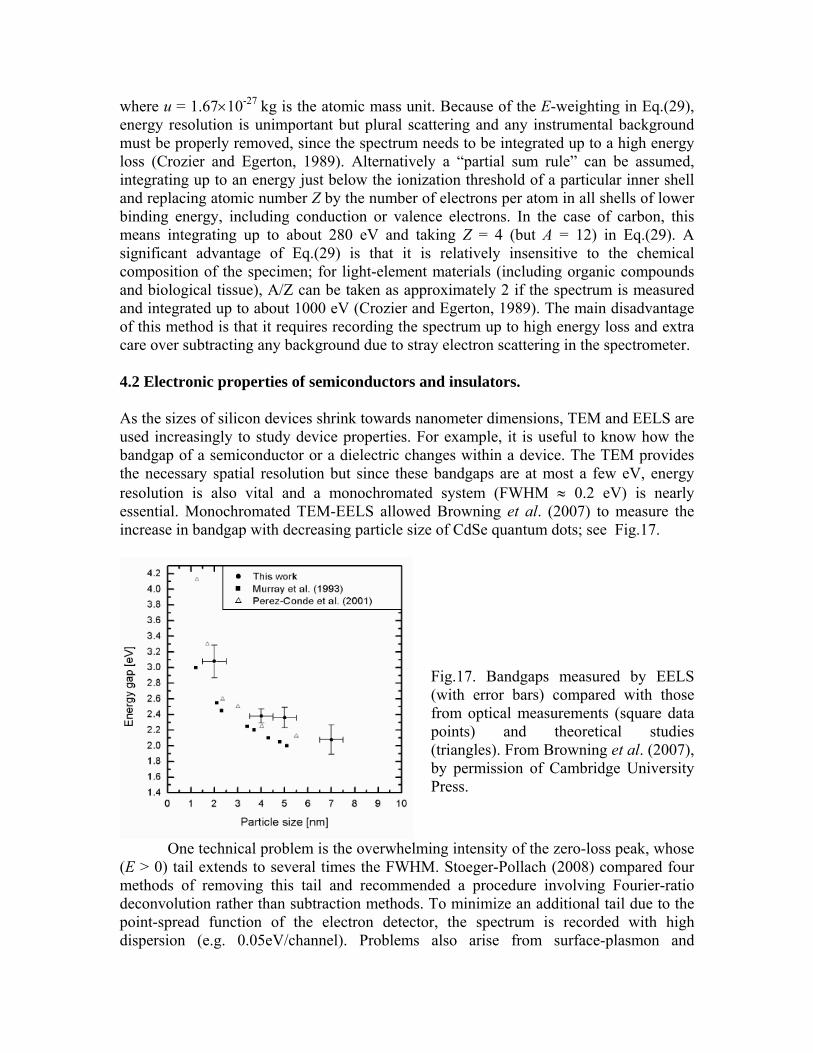
where u = 1.67×10⁻²⁷ kg is the atomic mass unit. Because of the E-weighting in Eq.(29), energy resolution is unimportant but plural scattering and any instrumental background must be properly removed, since the spectrum needs to be integrated up to a high energy loss (Crozier and Egerton, 1989). Alternatively a “partial sum rule” can be assumed, integrating up to an energy just below the ionization threshold of a particular inner shell and replacing atomic number Z by the number of electrons per atom in all shells of lower binding energy, including conduction or valence electrons. In the case of carbon, this means integrating up to about 280 eV and taking Z = 4 (but A = 12) in Eq.(29). A significant advantage of Eq.(29) is that it is relatively insensitive to the chemical composition of the specimen; for light-element materials (including organic compounds and biological tissue), A/Z can be taken as approximately 2 if the spectrum is measured and integrated up to about 1000 eV (Crozier and Egerton, 1989). The main disadvantage of this method is that it requires recording the spectrum up to high energy loss and extra care over subtracting any background due to stray electron scattering in the spectrometer. 4.2 Electronic properties of semiconductors and insulators. As the sizes of silicon devices shrink towards nanometer dimensions, TEM and EELS are used increasingly to study device properties. For example, it is useful to know how the bandgap of a semiconductor or a dielectric changes within a device. The TEM provides the necessary spatial resolution but since these bandgaps are at most a few eV, energy resolution is also vital and a monochromated system (FWHM ≈ 0.2 eV) is nearly essential. Monochromated TEM-EELS allowed Browning et al. (2007) to measure the increase in bandgap with decreasing particle size of CdSe quantum dots; see Fig.17.
Fig.17. Bandgaps measured by EELS (with error bars) compared with those from optical measurements (square data points) and theoretical studies (triangles). From Browning et al. (2007), by permission of Cambridge University Press.
One technical problem is the overwhelming intensity of the zero-loss peak, whose (E > 0) tail extends to several times the FWHM. Stoeger-Pollach (2008) compared four methods of removing this tail and recommended a procedure involving Fourier-ratio deconvolution rather than subtraction methods. To minimize an additional tail due to the point-spread function of the electron detector, the spectrum is recorded with high dispersion (e.g. 0.05eV/channel). Problems also arise from surface-plasmon and

retardation (Cerenkov) modes, which add peaks below 10 eV. These latter contributions can be minimized by using an off-axis detector or by subtracting the spectra recorded with small and large collection angles (Stoeger-Pollach, 2008), equivalent to a collection aperture with a central stop. Rafferty& Brown (1998) pointed out that the low-loss fine structure involves a joint density of states multiplied by a matrix element that differs in the case of direct and indirect transitions. Assuming no excitonic states, their analysis showed that the onset of energy-loss intensity at the bandgap energy Eg is proportional to (E - Eg)1/2 for a direct gap and (E-Eg)3/2 for an indirect gap. Cubic GaN is a direct-gap material whose inelastic intensity (after subtracting the zero-loss tail) fits well to (E - Eg)1/2 for E > Eg (Lazar et al., 2003). For E > Eg, there is some residual intensity that may be evidence of indirect transitions in a surface-oxide layer, since it can be fitted to a (E - Eg)3/2 function; see Fig.18.
Fig. 18. Inelastic intensity recorded from cubic GaN using a monochromated TEM-EELS system. Above the bandgap energy (Eg = 3.1 eV), data are fitted to the direct-gap expression (E - Eg)0.5, at lower energy to the indirect-gap expression (E - Eg)1.5 where Eg = 2 eV. From Lazar et al. (2003), copyright Elsevier. Figure 19 shows low-loss spectra recorded from the anatase phase of TiO2 (indirect gap ≈ 3.05eV) and from a related hydroxylated material H2Ti3O7 in the form of a 8nm-diameter multiwalled nanotubes. Below 5 eV, the spectra can be fitted to a (E-Eg)1.5 function but in the case of the nanotube, some additional intensity below 4 eV may indicate transitions involving defect states introduced by the hydroxyl groups (Wang et al., 2008b). Note that these fits were performed on the spectra recorded with an off-axis spectrometer-entrance aperture (K ~ 1 nm-1), in order to minimise unwanted surface-plasmon and Cerenkov-loss contributions. Conversely, an electron probe focused a few nm outside a nanotube or small particle (aloof mode) generates mainly surface rather than bulk-mode excitations.

Fig.19. Low-loss spectra from (a) H2Ti3O7 nanotube and (b) anatase TiO2, recorded as a function of the magnitude K of the inelastic-scattering vector. Insets at top show fits of the inelastic intensities to a (E-Eg)1.5 function. Reprinted with permission from Wang et al. (2008b), copyright American Institute of Physics.
Crystalline defects greatly affect the electrical and mechanical properties of materials, often adversely. High-resolution TEM can reveal the atomic arrangement of individual defects while EELS gives information on their local electronic structure and bonding. Combining this information may lead to an understanding of how the atomic structure and physical properties are related. Using a high-resolution STEM, Batson et al. (1986) could detect inelastic scattering due to localised states (within the 1.26eV bandgap of GaAs) at a single misfit dislocation. Although strong diffraction in a crystalline specimen makes the interpretation of inelastic scattering more complicated, channeling directs the electrons down atomic columns (if the beam is aligned with a crystal axis) and improves the spatial resolution (Loane et al., 1988). The high-resolution STEM uses an annular dark-field (ADF) detector that collects high-angle elastic scattering (proportional to Z2) that provides good atomic-number contrast in a high-resolution ADF image. Given adequate probe stability, this image allows the electron beam to be positioned on an atomic column and held there long enough to enable useful spectra to be recorded (Duscher et al., 1998). 4.3. Plasmon spectroscopy The plasmon energy is related to mechanical properties of a material; large Ep implies a high valence-electron density, arising from short interatomic distances and/or a large number of valence electrons per atom, both of which lead to strong interatomic bonding. More specifically, the elastic, bulk and shear modulus all correlate with the square of the plasmon energy, although there is a fair amount of scatter; see Fig.20. Oleshko and Howe (2007) used this relation to deduce the mechanical properties of metal-alloy precipitates too small to be probed by nanoindentation techniques. Gilman (1999) showed that Ep is also correlated with surface energy, Fermi energy, polarizability (for metals) and band gap (for semiconductors). The implications have yet to be explored.

Fig.20. Bulk modulus plotted against plasmon energy for various elements. Reprinted with permission from Oleshko and Howe (2007), copyright American Institute of Physics.
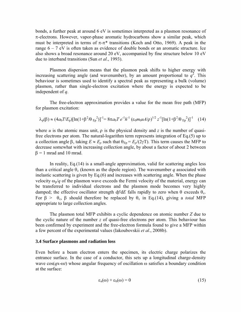
Daniels et al. (2003) used plasmon-loss mapping to investigate the mechanical properties of graphitic materials at a spatial resolution of 1.6 nm. By taking the ratio of intensities at 22 eV and 27 eV (either side of the σ+π-plasmon peak), they removed image contrast due to variations in specimen orientation and thickness. The plasmon energy itself was shown to be independent of specimen orientation but it increased after the specimen was annealed, indicating an increase in density and stronger bonding. Plasmon-loss spectroscopy or mapping is attractive for examining radiation-sensitive materials because the intensity greatly exceeds the core-loss intensity, so recording times (for achieving adequate signal/noise ratio) and radiation dose are much lower. Silicon nanoparticles could provide a light-emission system that would make optoelectronics compatible with silicon-processing technology. Yurtsever et al. (2006) fabricated a dispersion of Si particles, by annealing silicon oxide films deposited by chemical-vapour deposition of silane. Cross-sectional (XTEM) samples showed little contrast, the mean free paths for Si and SiO2 being very similar. However the plasmon energies differ: 17eV in Si but 23eV in SiO2, so energy-selective imaging gives a two-dimensional view of the nanoparticles. A more useful three-dimensional visualization was obtained with the aid of electron tomography, based on a series of TEM images recorded at many different specimen tilts (Frank, 2007; Gass et al., 2006); in this case, up to ±60° tilt in 4° increments. Computer software allowed alignment and reconstruction of the 17±2 eV images in three dimensions; see Fig. 21. The particles themselves have soft outlines, probably reflecting the delocalization of plasmon scattering (~2 nm, see later) but they were delineated by choosing a threshold intensity and representing the intensity contour as a mesh image. This technique made the particles more visible and showed that they have irregular shapes. Their complex morphology may explain the broad spectral range of photo- and electro-luminescence observed in this material, while the large surface area of each particle could account for the high efficiency of light emission.
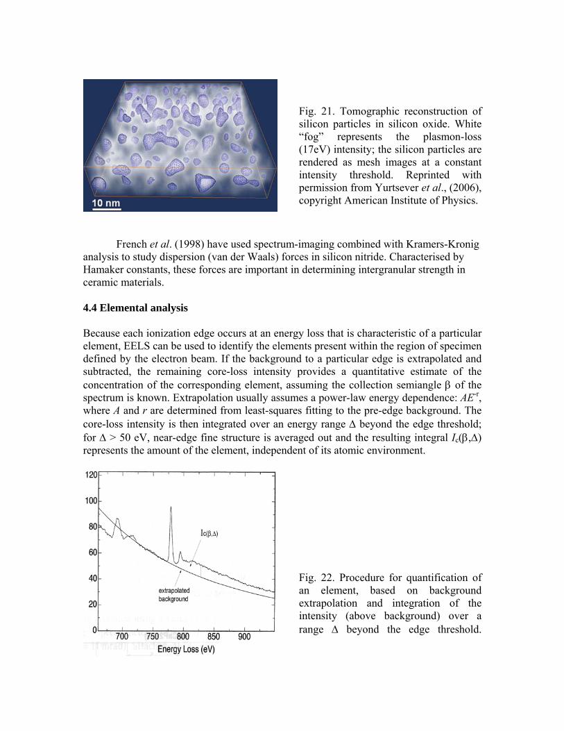
Fig. 21. Tomographic reconstruction of silicon particles in silicon oxide. White “fog” represents the plasmon-loss (17eV) intensity; the silicon particles are rendered as mesh images at a constant intensity threshold. Reprinted with permission from Yurtsever et al., (2006), copyright American Institute of Physics.
French et al. (1998) have used spectrum-imaging combined with Kramers-Kronig analysis to study dispersion (van der Waals) forces in silicon nitride. Characterised by Hamaker constants, these forces are important in determining intergranular strength in ceramic materials. 4.4 Elemental analysis Because each ionization edge occurs at an energy loss that is characteristic of a particular element, EELS can be used to identify the elements present within the region of specimen defined by the electron beam. If the background to a particular edge is extrapolated and subtracted, the remaining core-loss intensity provides a quantitative estimate of the concentration of the corresponding element, assuming the collection semiangle β of the spectrum is known. Extrapolation usually assumes a power-law energy dependence: AE-r, where A and r are determined from least-squares fitting to the pre-edge background. The core-loss intensity is then integrated over an energy range Δ beyond the edge threshold; for Δ > 50 eV, near-edge fine structure is averaged out and the resulting integral Ic(β,Δ) represents the amount of the element, independent of its atomic environment.
Fig. 22. Procedure for quantification of an element, based on background extrapolation and integration of the intensity (above background) over a range Δ beyond the edge threshold.

Although the angular distribution of scattering is a complicated mixture of elastic, plasmon and plural scattering, the areal density of the element (N atoms per unit area) can be estimated from the simple formula:
Ic(β,Δ) ≈ N Il(β,Δ)σ(β,Δ) (30) If the local specimen thickness t is known, the elemental concentration n is given by n = N/t. The quantity σ(β,Δ) is a partial cross section, calculated for core-loss scattering up to an angle β and energy range Δ beyond the threshold. For K-shells, this cross section is available from the hydrogenic model (Egerton, 1979); for other shells, Hartree-Slater calculations or experimental measurements are used (Rez, 1982; Hofer, 1987). The term Il(β,Δ) in Eq.(30) represents an integral of the low-loss spectrum up to an energy loss Δ, including the entire zero-loss peak. Both Ic and Il can be measured in arbitary units since only their ratio is required to deduce N; there is no need to calibrate the recorded intensities or measure the electron-beam current. For typical values of t and β, Eq.(30) makes approximate allowance for elastic and plural-inelastic scattering (Egerton, 1996).
As an example, Crozier (2007) used Eq.(30) to measure the amount of nitrogen,
oxygen and silicon within a STEM probe focused onto a thin Si3N4 membrane in the presence of water vapour. Decrease of nitrogen and the development of an oxygen K-edge within a few seconds indicated the transformation of silicon nitride into silicon oxide. Using the latter as a nanolithography mask offers the possibility of patterning at 15nm resolution.
Although Eq.(30) provides absolute (standardless) quantification, elemental ratios
are often more useful. Applying Eq.(30) to two elements (A and B) and dividing gives:
nA/nB = NA/NB = [IcA(β,Δ)/Ic
B(β,Δ)] [σcB(β,Δ)/σc
A(β,Δ)] (31) Since t and Il cancel, neither the low-loss region nor the specimen thickness is needed to obtain the concentration ratio nA/nB. Equation (30) also forms a basis for energy-selected imaging, where the aim is an elemental map showing the spatial distribution of a given element, the equivalent of an x-ray elemental map (Friel and Lyman, 2006). Division of the Ic and Il images roughly compensates for variations in elastic scattering (diffraction-contrast artifacts) although thickness variations still show up in the image. Alternatively, Ic can be displayed directly, provided the spectrum is recorded with a large collection aperture (β > 50 mrad) that admits most of the elastic scattering. With an aberration-corrected spectrometer and probe-forming lens, this simple procedure has been shown to provide elemental mapping down to the atomic scale; see Fig. 23.

Fig. 23. Atomic-scale elemental mapping: the 64×64-pixel images show columns of La, Ti, total and Mn atoms from (a) La-M, (b) Ti-L and (c) Mn-L edges recorded from La0.7Sr0.3MnO3 by spectrum-imaging. Reprinted from Muller et al. (2008), courtesy of American Association for the Advancement of Science (AAAS). The possibility of very high spatial resolution is one reason to prefer EELS to energy-dispersive x-ray spectroscopy (EDXS) as a method of elemental analysis in the TEM. Although EDXS provides a more convenient technique, avoiding the need for spectrometer alignment for example, its spatial resolution is often limited to several nm because of x-rays generated by scattered electrons and stray electrons in the TEM column. Also the energy resolution of EDXS is currently ~ 100eV, so the technique does not offer the kind of structural information that is available from EELS. However, recent improvements in the collection efficiency of x-ray detectors have made it possible to produce x-ray maps that give semi-quantitative information down to atomic dimensions (Watanabe et al., 2009; von Harrach, 2009; Zaluzec, 2009, 2010; D’Alfonso et al., 2010).
If the ratio of two core-loss signals is displayed, the result is an elemental-ratio image in which variations in specimen orientation, thickness and beam current are suppressed, according to Eq.(31). Dividing core-loss intensity by that of the preceding background gives a jump-ratio image showing the elemental distribution in a semi-quantitative way and with better signal/noise ratio than an elemental map and with variations in specimen orientation, thickness and beam current suppressed (Hofer et al., 1995; Crozier, 1995). Accurate subtraction of the background from the core-loss signal is difficult in some cases: where the elemental concentration is low or where two ionization edges are separated in energy by less than 50 eV. It is then preferable to represent the spectrum as a power-law background (arising from a plasmon peak, for example) and core-loss profile for each edge:
J(E) = AE-r + C1Jc1(E) + C2Jc2(E) + … (32) The core-loss profiles can be calculated or (better) measured using elemental standards of known thickness and composition. The weightings (C1, C2 …) of each contribution are adjusted by multiple least-squares (MLS) fitting and their values converted to relative concentrations, knowing an ionization cross section for each element (Leapman, 2004; Bertoni and Verbeeck, 2008).

The ability to record spectrum-image data results in a large amount of stored data, calling for an efficient method of extracting useful information such as multivariate statistical analysis (MVA or MSA). The most widely used multivariate method is principal component analysis (PCA) in which spectral components are ranked in terms of information content on a scree plot, enabling the useful components to be selected and distinguished from noise. Computer programs for PCA are now available; besides reducing the amount of human labor required to sort through the data, PCA can identify spectral artifacts and reject noise without sacrificing spatial resolution (Bosman et al, 2006; Lozano-Perez et al., 2009; de la Pena et al, 2011) 4.5 Spatial resolution of EELS The spatial resolution of an energy-loss spectrum or an energy-filtered image depends on many factors (Egerton, 2007). Some are instrumental and involve the electron optics of the TEM column; strongly excited lenses of small focal length (< 2mm) achieve low coefficients of spherical and chromatic aberration and a point resolution below 0.2 nm, while aberration correction gives further improvement. However, such high performance is only meaningful when the TEM has highly stable power supplies and is operated in an environment where changes in magnetic field, ambient pressure and temperature changes are minimised by careful room design (Muller et al., 2006).
Other resolution factors relate to the physics of electron scattering. Elastic scattering causes a broadening of a focused electron probe, by an amount that increases with specimen thickness (Goldstein et al., 1977). This broadening limits the resolution of x-ray emission spectroscopy but the effective broadening is less for EELS if an angle-limiting aperture is used to eliminate electrons scattered through larger angles. Beam broadening is also less in a crystalline specimen, as a result of electron channeling down atomic columns (Loane et al, 1988).
Although beam broadening can be minimized by using ultrathin specimen, there
is another factor that is independent of thickness and inherent to the inelastic scattering itself: delocalization of the scattering. Delocalization can be understood in a semi-quantitative way in terms of a single-scattering model, treating beam broadening as a separate effect and regarding the delocalization distance L as a wave-optical resolution limit arising from the limited angular range of the inelastic scattering:
L50 = 0.52 λ/⟨θ⟩ (33)
Equation (33) is essentially the Rayleigh criterion for resolution, with the factor 0.52 chosen to reflect the fact that L50 is a diameter containing 50% of the inelastic scattering; λ is the transmitted-electron wavelength and ⟨θ⟩ is a median angle that contains 50% of the inelastic scattering, small enough so that ⟨θ⟩ ≈ sin⟨θ⟩ in the Rayleigh formula. For a Lorentzian angular distribution of inelastic scattering, ⟨θ⟩ ≈ (θEθc)1/2 where θc is the highest angle that reaches the electron detector. Equation (33) provides a fair

approximation to both measurements and more exact calculations of delocalization distance; see Fig.24.
Fig. 24. Delocalization of inelastic scattering as a function of energy loss, for 100keV incident energy. The dashed curve shows Eq.(33) with median scattering angle evaluated from Bethe atomic scattering theory, solid line with ⟨θ⟩ based on a plasmon model. From Egerton (2007), copyright Elsevier.
As seen in Fig. 24, delocalization amounts to 2 – 3 nm for plasmon losses, which may account for the fuzziness in Fig.21. However, L50 falls with increasing energy loss (broader angular distribution) and is below 0.5 nm for E > 100 eV. This explains why, despite the low intensity, higher-energy ionization edges are preferred when aiming for atomic-resolution spectroscopic imaging (Kimoto et al., 2007; Muller et al., 2008).
The dashed curve in Fig. 24 assumes a Lorentzian angular distributionof core-loss
scattering. If core losses well above an ionization-edge threshold are measured, ⟨θ⟩ will approximate to the larger Bethe-ridge angle and the value of L50 is reduced (Kimoto et al, 2007).
If the spectrometer collection aperture cuts off an appreciable part of the
scattering, delocalization effects are more complicated. The Bethe atomic theory of scattering can be generalised to give the following expression for inelastic cross section:

σ = 2πm/(k0h2) ∫ ∫ ∫ ψ0*(r,z) W(r,r’) ψ0(r’,z) dr dr’ dz (34)
Here ψ0 is a wavefunction of the incident electron; the integrations are over specimen thickness (0 < z < t) and over radial coordinates perpendicular to z. The function W is an effective nonlocal potential, related to the mixed dynamical form factor (Kohl and Rose, 1985; Schattschneider et al., 2000). It includes the effect of probe and detector geometry and is a function of two independent spatial coordinates (r and r’). As a result, Eq.(34) incorporates the effect of the phase of the transmitted electron and its diffraction by the specimen, making σ a sensitive function of the angle between the electron and the crystal. Calculations show that the inelastic intensity is not always proportional to the z-integrated current density, implying that energy-filtered STEM images cannot always be visually interpreted but require computer modeling to be understood on an atomic scale (Oxley and Pennycook, 2008).
As a practical example of an atomic-resolution study, Fig. 25 shows how M45-
edge (850eV) spectra were used to identify which atomic columns contained lanthanum in ADF-STEM images of La-doped calcium titanate; Intensity simulations indicated that these columns contained only a single La atom. With the aid of electron-channeling calculations, it may even be possible to use the core-loss intensity to estimate the depth of each atom, thereby providing three-dimensional atomic imaging (Varela et al., 2004).
Fig. 25. (a) Annular-dark-field Z-contrast STEM image of calcium titanate containing 4% La. (b) Core-loss spectra taken with the beam stationary at positions 1 – 6, demonstrating that atomic column at 3 contained La, believed to be a single atom. Reprinted with permission from Varela et al., (2004), Phys. Rev. Lett. 92, 095502-1. Copyright (2004) by the American Physical Society.
4.6 Magnetic measurements EELS has been used to investigate magnetic (electron-spin) properties of materials (Schattschneider et al., 2008). This kind of measurement can be achieved using circularly polarised x-rays but rather than using a spin-polarised electron source (whose intensity is weak), a regular TEM is used together with an energy-loss spectrometer or omega filter. The experiment involves measuring core-loss spectra at two carefully chosen locations in the diffraction plane. Under dynamical diffraction conditions, inelastic interference due to MDFF terms increases or decreases the electron intensity by several percent (at the L3 and L2 white-line peaks of Co, Fe or Ni), dependent on the spin direction and the location of the detector in the diffraction plane. Subtraction of the two spectra then gives a signal of opposite sign at the two edges and although the signal is weak and noisy, a resolution down to 6 nm has been achieved for the L23 edges of Co. This method has been applied to mineralized magnetite crystals in magnetotactic bacteria and a spatial resolution of 2 nm reported (Stöger-Pollach et al., 2011).
An alternative procedure that may be more easily applicable (since it does not require a specimen of specially chosen thickness and orientation) involves the use of a specially-fabricated aperture to produce a vortex beam of electrons, with orbital angular momentum. This idea has been successfully tested on a ferromagnetic iron specimen (Verbeeck et al., 2010). 4.7 Radiation damage In many materials, the practical limit to spatial resolution is set by radiation damage. For organic and some inorganic compounds, the damage mechanism is radiolysis (ionization damage): the breaking of chemical bonds as a result of the inelastic scattering. Since this same scattering provides the EELS signal, the signal/damage ratio is typically independent of accelerating voltage; damage occurs even for low-energy incident electrons, as used in HREELS (Chen et al., 2002) but is confined to the surface of the specimen. X-rays, used in XAS, also cause radiolysis, although for core-loss fine-structure studies the damage has been estimated to be a factor of several hundred less, dependent on the width of the energy range analysed (Rightor et al., 1997). This advantage arises because x-ray photons excite only the transitions being measured whereas electrons excite all energy losses simultaneously. X-ray damage is estimated (Henderson, 1995) to be a factor of 103-104 larger than for electrons when the information being sought comes from elastic scattering (diffraction).
For metallic and semi-metallic specimens, there is no radiolysis but displacement damage (due to elastic scattering) occurs at high radiation dose. This process occurs only above a threshold incident energy, which is above 200 keV for bulk displacement and medium- or high-Z elements. However, the displacement of surface atoms (electron-beam sputtering) has a lower energy threshold (Egerton et al., 2006). Although the

required electron dose is high, sputtering may be quite rapid in a focused aberration-corrected electron probe, where the current density can exceed 106 A/cm2.
Radiation damage limits the number of electrons incident on each resolution element of size d to (Dc/e)d2, where e is the electronic charge and Dc is the critical dose (charge per unit area) needed to cause the damage. Even if all of them are collected, the number of inelastically scattered electrons (the EELS signal) is therefore limited to n ≈ (t/λi)(Dc/e)d2 , where t is specimen thickness and λi is some effective mean free path that depends on the specimen and the inelastic scattering process involved. Associated with these n electrons is an electron-beam shot noise n1/2
, giving a signal/noise ratio SNR = n/n1/2
= n1/2, assuming Poisson statistics where the standard deviation is the square root of the mean value. Combining the two expressions gives (t/λi)(Dc/e)d2 = n = (SNR)2 and taking SNR = 5 (the so-called Rose criterion for visibility), the resolution limit imposed by radiation damage is:
d ≈ 5(λi /t)1/2(e/Dc)1/2 (35)
Estimates of d are given in Table 3, which shows that radiation damage sets the spatial-resolution limit (d > atomic dimensions) for organic specimens and some inorganic compounds. For more radiation-resistant specimens, other factors (as discussed in Section 4.5) are likely to be more important, except perhaps for core-loss spectroscopy using high-E edges (Egerton, 1996). Damage mechanism
Type of specimen
Damage dose Dc (C/cm2)
d (nm) for low-loss EELS
d (nm) for 350eV-EELS
radiolysis organic 10-3 – 1 < 0.5 1 − 300 radiolysis inorganic 0.1 − 106 < 0.05 0.01 − 30 sputtering metallic 2000 – 40,000 < 5×10⁻⁴ < 0.2 Table 3: Electron dose to produce damage and the corresponding limit to spatial resolution, for 20nm specimen thickness and 200 keV incident energy (Egerton, 2007). The spread in Dc values corresponds to different specimen materials within each category. The last column relates to the detection of 10% calcium (at SNR = 5) from the L23-edge. Although radiation damage acts as a limit to any electron-beam measurement, EELS offers a method of characterising this damage for a particular type of specimen. Change in thickness (mass loss) can be monitored from the low-loss region and the loss of specific elements from ionization edges (Egerton, 2011). 4.8 Use of chemical shifts and near-edge fine structure The oxidation state of an element can be judged from chemical shift of an ionization edge or from near-edge fine structure, such as the L3/L2 ratio in the case of a transition metal. Daulton et al. (2003) used both techniques and plotted chromium L3/L2 ratios and L3

threshold energy for a variety of inorganic compounds with Cr in oxidation states between 2 and 6. As seen in Fig.26, the data cluster into groups, confirming a correlation between both types of measurement. They also examined Shewanella oneidensis bacteria, using an environmental cell that kept the specimen hydrated in the TEM, and found that the resulting data fell into the Cr(III) region (see Fig.5D), confirming that these bacteria may be active sites for the reduction of the toxic Cr(VI) species in chromium-contaminated water.
Fig. 26. Chromium L3/L2 ratio plotted against L3 threshold energy for inorganic compounds (data points within curved boundaries) and measured for S. oneidensis (central data point with large error bars). Reproduced from Daulton et al. (2003), with permission of Cambridge University Press.
Energy-filtered (EFTEM) imaging has been used to plot L3/L2 ratios as an intensity map, displaying variations in the valence state of Mn and Co in mixed-valence specimens (Wang et al., 1999). The existence of a chemical shift should be considered when using core-loss spectroscopy to examine interfaces, for example using the “spatial difference” method (Muller et al., 1998).
As integrated circuits become increasingly miniaturized, the thickness of the gate
oxide in a field-effect transistor has fallen towards 1 nm in order to reduce gate voltage and power dissipation. Since this corresponds to only five Si atoms across, the properties of the oxide might be expected to depart considerably from the bulk values. High-resolution STEM of cross-sectional (XTEM) specimens, combined with core-loss EELS, provides a way of investigating these effects (Batson, 1993). Figure 27 shows how the background-subtracted oxygen-K edge changes as the STEM probe approaches the Si interface from a native oxide. The threshold shifts downwards by 0.3 eV, indicating a reduced bandgap, and the sharp threshold peak disappears. This peak arises from backscattering of the ejected core electron from nearest-neighbour oxygen atoms (Si atoms backscatter much less than oxygen), so its absence close to the interface indicates a silicon-rich environment: a suboxide SiOx where x < 2. Similar results were obtained for thermally grown oxide, as used in device fabrication. From analysis of the two components of the near-edge structure, the suboxide was estimated to have a width of 0.75 nm, out of a total thermal-oxide width of 1.6 nm (Muller et al., 1999).

Fig. 27. Oxygen K-loss spectra from the native oxide on silicon (solid line b) and from region near the Si interface (data a). Reproduced from Muller et al. (1999), with permission of Nature Publishing Group.
In general, near-edge fine structure can give useful information on interatomic bonding (Browning et al. 1997) but for quantitative results it is important to avoid edges that are strongly affected by the presence of the core hole, such as cations in ionic materials (Rez and Muller, 2008). Principal-component analysis can isolate the different fine-structure components present in a spectrum-image dataset and produce a map showing chemical and bonding information. Since one of the components is random noise, this technique can also reduce the image noise without sacrificing spatial or energy resolution (Bosman et al., 2006). 5. Practical aspects of EELS-data acquisition Table 4 lists some of the possible procedural choices that may be options when energy-loss data are acquired. As indicated in Section 2, there are several ways of displaying the information obtained from EELS. The energy-loss spectrum yields quantitative information, such as the local thickness, chemical composition, crystallographic and electronic structure of a defined region. An energy-filtered image is more useful for revealing variations in thickness, composition or bonding, or simply for optimizing the contrast arising from structural features. A spectrum-image combines spatial and energy-loss information, and allows sophisticated procedures such as multivariate statistical analysis to be applied to stored data. Energy-filtered diffraction is useful for the quantitative interpretation of diffraction patterns, for examining the directionality of chemical bonding, or for finding out what scattering processes are contributing to the energy-loss spectrum of a particular specimen. The three basic types of TEM-EELS systems were described earlier (Fig. 3). A spectrometer mounted beneath the TEM column is the most common choice for acquiring energy-loss spectra and a Gatan GIF system can also obtain energy-filtered images and diffraction patterns. An in-column filter is convenient for EFTEM because the energy-filtered image appears on the usual TEM screen; spectroscopy and spectrum-imaging is possible but the latter is less dose-efficient and its spectral information requires careful drift correction and possibly interpolation to obtain good energy resolution.

parameter options advantages type of data energy-loss spectrum
energy-filtered image spectrum-image energy-filtered DP
quantitative data from defined area spatial distribution, at least qualitative large information content physics revealed
instrumentation post-column spectrometer in-column filter dedicated STEM
good choice for spectroscopy convenient for EFTEM ideal for spectrum-imaging
incident energy high (e.g. 200 kV) low (e.g. 60 keV)
ionization edges more visible reduced damage, Cerenkov effects
TEM mode image on screen DP on screen
spatial location of EELS easy more precise spatial location
collection angle β < 10 mrad β> 100 mrad
dipole conditions, high edge jump ratio good for E > 1 keV and log-ratio method
energy dispersion dE/dx > 1 eV/channel dE/dx < 0.1 eV/channel
large energy losses measurements in low-loss region
recording time short time long time
less drift, less radiation damage better statistics
number of readouts
small large
relatively low readout noise better dynamic range & drift correction
Table 4: Options involved in the acquisition of energy-loss data. High incident energy makes it easier to obtain good spatial resolution in the TEM, although aberration correctors make this less necessary. Since high E0 is equivalent (in terms of the amount of scattering) to a thinner specimen, this condition increases the signal/background ratio at ionization edges, reducing the need for deconvolution and making quantitative analysis more feasible and accurate. However, it results in a very strong zero-loss peak, whose tail may interfere with low-loss fine structure – for example to measure bandgap in a semiconductor. Lower E0 also reduces any Cerenkov contribution below 5 eV and may avoid or reduce knock-on damage effects (atomic displacement in the bulk or sputtering from specimen surfaces). In the case of a below-column spectrometer, TEM image mode makes it easy to see what region of specimen is giving rise to the energy-loss spectrum (just by lowering the viewing screen) but aberrations of the imaging lenses may preclude precise spatial localization. The use of TEM diffraction mode allows small areas to be defined by means of a very small probe. Alternatively, diffraction mode with a large-diameter beam provides high intensity (useful for core-loss spectroscopy) since electrons from the entire beam area contribute (the spectrometer entrance aperture accepts most of the scattering). In both cases, the centre of the diffraction pattern should be aligned to the centre of the spectrometer entrance aperture, adjusting manually for maximum intensity. The spectrum collection semi-angle β is determined by the TEM objective aperture or (in diffraction mode) by the spectrometer entrance aperture. Small β increases signal/background ratio art ionization edges and minimizes non-dipole scattering (necessary when applying Kramers-Kronig sum rule, for example). Large β simplifies

thickness measurement by the log-ratio method and may be preferable for ionization edges above 1 keV in order to achieve adequate intensity. Long recording time of the spectrum minimizes statistical (shot) noise, of prime importance for recording ionization edges. Saturation of the electron detector provides one time limit, typically a fraction of a second for the low-loss region, especially if the zero-loss peak is included. However, this limit can be extended by combining multiple readouts, occasionally at the expense of readout noise. Multiple readouts also allow correction for energy drift, due to change in accelerating voltage or spectrometer current, by programming the data-acquisition computer to recognize and aligning a prominent spectral feature. Another time limit comes from specimen drift, although this can sometimes be compensated electronically. A more fundamental limit arises from radiation damage, whose severity varies greatly depending on the type of specimen (Table 3, p.38). Damage in conducting specimens (e.g. metals) arises from knock-on processes and can sometimes be avoided by reducing the incident energy below some threshold. Damage in organic and inorganic compounds is usually due to radiolysis, which can be reduced by a modest factor (e.g. 3) by cooling the specimen. 6. Further reading
This review is an updated version of Egerton (2009). Further information on the basic theory and practice of TEM-EELS is given in introductory form by Brydson (2001), in greater detail by Egerton (2011), and in two multi-author volumes edited by Reimer (1995) and Ahn (2004). Research articles on TEM-EELS are to be found in microscopy journals, especially Ultramicroscopy and Micron, and scattered among various physics and materials-science journals. A recent review by Spence (2006) concentrates on STEM, channeling effects and applications to glasses and nanotubes. A short review of biophysical applications has been given by Leapman (2004b). References Ahn, C.C.(ed.) (2004) Transmission Electron Energy Loss Spectrometry in Materials Science and the EELS Atlas (John Wiley & Sons, New York). Ahn C.C. and Krivanek O.L. (1983) EELS Atlas. (Gatan Inc., Warrendale, PA); available from Gatan (www.gatan.com). Alexander, D.T.L, Crozier, P.A. and Anderson, J.R. (2008) Brown carbon spheres in East Asian outflow and their optical properties. Science 321, 833-836. Barbarez, M.K., Das Gupta, D.K. and Hayward, D. (1977) On the mechanisms of characteristic electron energy loss spectra of polymers. J. Phys. D: Appl. Phys. 10, 1789-1800. Batson, P. E. (1993) Simultaneous STEM imaging and electron energy-loss spectroscopy with atomic column sensitivity. Nature 366, 727-728.

Batson, P.E. (2008) Local crystal anisotropy obtained in the small probe geometry. Micron 39, 648–652 Batson, P.E., Kavanah, K.L, Woodall, J.M. and Mayer, J.M. (1986) Electron-energy-loss scattering near a single misfit dislocation at the GaAs/GaInAs interface. Phys. Rev. Lett. 57, 2719-2732. Bertoni, G. and Verbeeck, J. (2008) Accuracy and precision in model based EELS quantification Ultramicroscopy 108, 782–790 Bosman, M., Watanabe, M., Alexander, D.T.L. and Keast, V.J. (2006) Mapping chemical and bonding information using multivariate analysis of electron energy-loss spectrum images. Ultramicroscopy 106, 1024–1032. Brown, L.M. (1997) A synchrotron in a microscope. Proc. EMAG97 (Inst. Phys. Conf. Ser. No. 153), 17-21. Browning, N.D., Wallis, D.J., Nellist, P.D. and Pennycook, S.J. (1997) EELS in the STEM: Determination of materials properties on the atomic scale. Micron 28, 333-348. Browning, N.D. Arslan, I., Bradley, J.P., Chi, M., Dai, Z., Erni, R., Herrera, M., Okamoto, N.L., Ramasse, Q. (2007) Aberration Corrected and Monochromated TEM/TEM for Materials Science. Microsc. Microanal .13(Suppl 2), 1180-1181 CD. Brydson, R. (2001) Electron Energy Loss Spectroscopy (Bios, Oxford). Y. Chen, R.E. Palmer, E.J. Shelley, J.A. Preece (2003) HREELS studies of gold nanoparticles with dialkyl sulphide ligands. Surf. Sci. 502/503, 208-213. Crozier, P.A. (1995) Quantitative elemental mapping of materials by energy-filtered imaging. Ultramicrosopy 58, 157-174.
Crozier, P.A. (2007) Nanoscale oxide patterning with electron-solid-gas reactions. Nano Letters 7, 2395-2398. Crozier, P.A. and Egerton, R.F. (1989) Mass thickness determination by Bethe-sum-rule normalization of the electron energy-loss spectrum. Ultramicroscopy 27, 9-18. D’Alfonso, A.J., Freitag, B., Klenov, D. And Allen, L.J. (2010) Atomic-resolution chemical mapping using energy-dispersive x-ray spectroscopy. Phys. Rev. B 81, 100101 (4 pages). Daniels, H.R., R. Brydson, A. Brown, B. Rand (2003) Quantitative valence plasmon mapping in the TEM: viewing. Ultramicroscopy 96, 547–558 Daulton, T.L., Little, B.J. and Lowe, K. (2003) Determination of chromium oxidation state in cultures of dissimilatory metal reducing bacteria by electron energy loss spectroscopy. Microsc. Microanal. 9 (Suppl. 2), 1480-1481. De la Pena, F., Berger, M.-H., Hochepied, J.-F., Dynys, F., Stephan, O. and Walls, M. (2011) Mapping titanium and tin oxide phases using EELS: An application of independent component analysis. Ultramicroscopy 111, 169-176.

Duscher, G., Browning, N. D., and Pennycook, S. J. (1998) Atomic column resolved electron energy-loss spectroscopy. Phys. Stat. Solidi A 166, 327-342: Eberlein, T. U., Bangert, U., Nair, R.R., Jones,R., Gass, M., Bleloch, A.L., Novoselov, K.S., Geim, A. and Briddon, P.R. (2008) Plasmon spectroscopy of free-standing graphene films. Phys. Rev. B 77, 233406. Egerton, R.F. (1979) K-shell ionization cross sections for use in microanalysis. Ultramicroscopy 4, 169-179. Egerton, R.F. (2007) Limits to the spatial, energy and momentum resolution of electron energy-loss spectroscopy. Ultramicroscopy 107, 575-586. Egerton, R.F. (2009) Electron energy-loss spectroscopy in the TEM. Rep. Prog. Phys. 72, 016502 (25pp). Online at stacks.iop.org/RoPP/72/016502 Egerton, R.F. (2011) Electron Energy-Loss Spectroscopy in the Electron Microscope, 3rd Edition (Springer, New York). Egerton, R.F. and Whelan, M.J. (1974). The electron energy-loss spectrum and band structure of diamond. Phil. Mag. 30, 739-749. Egerton, R.F., Qian, H., Malac, M. (2006a) Improving the energy resolution of X-ray and electron energy-loss spectra. Micron 37, 310–315. Egerton, R.F. Wang, F. and Crozier, P.A. (2006b) Beam-induced damage to thin specimens in an intense electron probe. Microscopy and Microanalysis 12, 65-71. Erni, R. and Browning, N.D. (2008) The impact of surface and retardation losses on valence electron energy-loss spectroscopy. Ultramicroscopy 108, 84–99 Fano, U. (1956) Differential inelastic scattering of relativistic charged particles. Phys. Rev. 102, 385-387. Frank, J. (2007) Electron Tomography: Three-Dimensional Imaging with the Transmission Electron Microscope, 2nd Ed .(Plenum, New York). Fransen, M.J., van Rooy, T.L. and Kruit, P. (1999) Field emission energy distribution from individual multi-walled carbon nanotubes. Applied Surface Science 146, 312-327. French, R.H., Muellejans, H., Jones, D.J., Duscher, G., Cannon, R.M. and Ruehle, M. (1998) Dispersion forces and Hamaker constants for intergranular films in silicon nitride from spatially resolved-valence elecrton energy loss spectrum imaging. Acta mater. 46, 2271-2287. Friel, J.J. and Lyman, C.E. (2006) X-ray mapping in electron-beam instruments. Microscopy and Microanalysis 12, 2-25. Gass, M.H., Koziol, K., Windle, A.H. and Midgley, P.A. (2006) Four-dimensional spectral tomography of carbonaceous nanocomposites. Nano Lett. 6, 376-379.

Gilman, J. (1999). Plasmons at shock fronts. Phil. Mag. 79, 643-654. Gloter, A., Douiri, A., Tence, M., Imhoff, D., Colliex, C. (2003) Improving energy resolution of EELS spectra: an alternative to the monochromator solution. Ultramicroscopy 96, 385–400. Goldstein, J.I., Costley, J.L., Lorimer, G.W. and Reed, S.J.B. (1977) Quantitative analysis in the electron microscope. Scanning Electron Microscopy, Part 1, 315-324. Haider, M., Uhlemann, S., Schwan, E., Rose, H., Kabius, B. and Urban, K. (1998) Electron microscopy image enhanced. Nature 392, 768-769. Hébert,_C., Schattschneider, Franco, P.H., and Jouffrey, B. (2006) ELNES at magic angle conditions. Ultramicroscopy 106, 1139–1143 Hébert, C. (2007) Practical aspects of running the WIEN2k code for electron spectroscopy. Micron 38, 12-28. Henderson, R. (1995) The potential and limitations of neutrons, electrons and X-rays for atomic resolution microscopy of unstained biological molecules, Quart. Rev. Biophys. 28, 171–193. Hofer, F. (1987). EELS quantification of M edges by using oxidic standards. Ultramicroscopy 21, 63-68. Hofer, F., Warbichler, P. and Grogger, W. (1995) Characterization of nanometer sized precipitates in solids by electron spectroscopic imaging. Ultramicroscopy 59, 15-31. Hu, X., Sun, Y. and Yuan, J. (2007). Multivariate statistical analysis of electron energy-loss spectroscopy in anisotropic materials. Ultramicroscopy 108, 465-471. Iakoubovskii, K., Mitsuishi, K., Nakayama, Y. and Furuya, K. (2008a). Thickness measurements with electron energy loss spectroscopy, Microscopy Research and Technique 71, 616-631. Iakoubovskii, K., Mitsuishi, K., Nakayama, Y.and Furuya, K. (2008b) Mean free path of inelastic electron scattering: Material dependence. Phys. Rev. B 77, 104102. Ibach, H. and Mills, D.L. (1982), Electron Energy-Loss Spectroscopy and Surface Vibrations, Academic Press, New York. Inokuti, M. (1979) Inelastic collisions of fast charged particles with atoms and molecules − The Bethe theory revisited. Rev. Mod. Phys. 43, 297-343. Itskovsky, M.A., Cohen, H. and Maniv, T. (2008) Far-field interaction of focused relativistic electron beams in electron energy loss spectroscopy of nanoscopic platelets. Phys. Rev. B 78, 045419. Jeanguiillaume, C. and Colliex, C. (1989) Spectrum-image: the next step in EELS digital acquisition and processing. Ultramicroscopy 78, 252-257. Johnson, D.W. and Spence, J.C.H. (1974). Determination of the single-scattering probability distribution from plural-scattering data. J. Phys. D (Appl. Phys.) 7, 771-780.

Jouffrey, B., Schattschneider, P. and Hebert, C. (2004) The magic angle: a solved mystery. Ultramicroscopy 102, 61-66. Keast, V.J.(2005) Ab initio calculations of plasmons and interband transitions in the low-loss electron energy-loss spectrum. Journal of Electron Spectroscopy and Related Phenomena 143, 97–104. Keil, P. (1968) Elektronen-Energieverlustmessungen und Berechnung optischer Konstanten: II Kaliumbromid. Z. Phys. 214, 266-284. Kesmodel, L. L. (2006) High-Resolution electron energy-loss spectroscopy (HREELS). In: Encyclopedia of Surface and Colloid Science, 2nd edition, Eds. P. Somasundaran and A. Hubbard. Taylor and Francis. Kimoto, K. and Matsui, Y (2002) Software techniques for EELS to realize about 0.3 eV energy resolution using 300kV FEG-TEM. J. Microsc. 208, 224–228. Kimoto, K., Ishizuka, K., Mizuguchi, T., Tanaka, I., Matsui, Y. (2003) The study of Al-L23 ELNES with resolution-enhancement software and first-principles calculation. J. Electron Microsc. 36, 299–303. Kimoto, K., Asaka, T., Nagai, T., Saito, M., Matsui, Y. and Ishizuka, K. (2007) Element-selective imaging of atomic columns in a crystal using STEM and EELS. Nature 450, 702-704. Kimoto, K., Ishizuka, K., and Matsui, Y. (2008) Decisive factors for realizing atomic-column resolution using STEM and EELS. Micron 39, 257-262. Klie, R.F., Zhu, Y., Schneider, G. and Tafto, J. (2003) Experimental probing of the anisotropy of the empty p states near the Fermi level in MgB2. Appl. Phys. Lett. 82, 4316-4318. Koch, E.E. and Otto, A. (1969) Characteristic energy losses of 30 keV-electrons in vapours of aromatic hydrocarbons. Optics Communications 1, 47-49. Kohl, H. and Rose, H. (1985) Theory of image formation by inelastically scattered electrons in the electron microscope. Adv. Electron. Electron Phys. 65, 175-200. Krause, M.O. and Oliver, J.H. (1979) Natural widths of atomic K and L levels. J. Phys. Chem. Ref. Data 8, 128-143. Krishman, V. and Ritchie, R.H. (1970) Anomalous damping of volume plasmons in polycrystalline materials. Phys. Rev. Lett. 24, 1117-1119. Krivanek, O.L., Dellby, N., and Lupini (1999) Towards sub-Å electron beams. Ultramicroscopy 78, 1 - 11. Krivanek, O.L., Dellby, N., Keyse, R.J., Murfitt, M.F., Own, C.S. and Szilagyi, Z.S. (2008) Advances in Aberration-Corrected STEM and EELS, in: Advances in Imaging and Electron Physics, ed. P.W. Hawkes. Kröger,E. (1968) Berechnung der Energieverluste schneller Elektronen in dünnen Schichten mit Retardierung. Z. Physik 216, 115–135.
Lazar, S., Botton, G.A., Wu, M.-Y., Tichelaar, F.D. and Zandbergen, H.W. (2003) Materials science applications of HREELS in near edge structure analysis and low-energy loss spectroscopy. Ultramicroscopy 96, 535-546. Lazar, S., Botton, G.A., Zandbergen, H.W. (2006) Enhancement of resolution in core-loss and low-loss spectroscopy in a monochromated microscope. Ultramicroscopy 106, 1091–1103. Leapman R.D. (2004a). EELS Quantitative Analysis. in: Transmission Electron Energy Loss Spectrometry in Materials Science and The EELS Atlas (second edition). (Ahn C.C., ed., Wiley-VCH Verlag GmbH), 49–96. Leapman, R.D. (2004b) Novel techniques in electron microscopy. Current Opinion in Neurobiology 14, 591–598. Leapman, R.D., Fejes, P.L. and Silcox, J. (1983) Orientation dependence of core edges from anisotropic materials determined by inelastic scattering of fast electrons. Phys. Rev. B 28, 2361-2373. Lenz, F. (1954) Zur Streuung mittelschneller Elektronen in kleinste Winkel. Z. Naturfrosch. 9A, 185-204. Loane, R.F., Kirkland, E.J. and Silcox, J. (1988) Visibility of single heavy atoms on thin crystalline silicon in simulated annular dark-field STEM images. Acta. Cryst. A 44, 912-927. Lozano-Perez, S., de Castro Bernal, V. and Nicholls, R.J. (2009) Achieving sub-nanometre particle mapping with energy-filtered TEM. Ultramicroscopy 109, 1217-1228. Møller, C. (1932) Zur Theorie des Durchgangs schneller Elektronen durch Materie. Ann. Phys. (Leipzig) 14, 531-585. Moreno, M.S., Lazar, S., Zandbergen, H.W. and Egerton, R.F. (2006) Accuracy of the calculated unoccupied states in GaN phases as tested by high-resolution electron energy-loss spectroscopy. Phys. Rev. B 73, 073308. Moreno, M.S., Jorissen, K. and Rehr, J.J. (2007) Practical aspects of electron energy-loss spectroscopy (EELS) calculations using FEFF8. Micron 38, 1-11. Muller, D.A. (1999) Why changes in bond lengths and cohesion lead to core-level shifts in metals, and consequences for the spatial difference method. Ultramicroscopy 78, 163-174. Muller, D.A., Singh, D.J., Silcox, J. (1998) Connections between the electron energy-loss spectra, the local electronic structure, and the physical properties of a material: a study of nickel aluminum alloys. Phys. Rev. B 57, 8181–8202. Muller, D.A., T. Sorsch, S. Moccio, F. H. Baumann, K. Evans-Lutterodt & G. Timp (1999) The electronic structure at the atomic scale of ultrathin gate oxides. Nature 399, 758-761. Muller, D.A., Kirkland, E.J., Thomas, M.G, Grazul, J.L., Fitting, L. and Weyland, M. (2006) Room design for high-performance electron microscopy. Ultramicroscopy 106, 1033–1040

Muller, D.A., Kourkoutis, L.F., Murfitt, M., Song, J.H., Hwang, H.Y.,Silcox, J., Dellby, N. and Krivanek, O.L. (2008) Atomic-scale chemical imaging of composition and bonding by aberration-corrected microscopy. Science 319, 1073. Nehayah, J., Kociak, M., Stéphan, O., Garcia de Abajo, F.J, Tencé, M., Henrard, L., Taverna, D., Pastoriza-Santos, I., Liz-Marzán, L.M. and Colliex, C. (2007) Mapping surface plasmons on a single metallic nanoparticle. Nature Physics 3, 348-352. Oleshko, V.P and Howe, J.M. (2007). In situ determination and imaging of physical properties of metastable and equilibrium precipitates using valence electron energy-loss spectroscopy and energy-filtering transmission electron microscopy. J. Appl. Phys. 101, 054308. Overwijk, M.H.F. and Reefman, D. (2000) Maximum-entropy deconvolutionapplied to electron energy-loss spectroscopy. Micron 31, 325–331. Oxley, M.P. and Pennycook, S.J. (2008) Image simulation for electron energy loss spectroscopy. Micron 39, 676-684. Powell, C.J. and Swan, J.B. (1960) Effect of oxidation on the characteristic loss spectra of aluminum and magnesium. Phys. Rev. 118, 640-643. Raether, H. (1980) Excitation of Plasmons and Interband Transitions by Electrons. Springer-Verlag, Berlin. Rafferty, B. and L. M. Brown, L.M. (1998) Direct and indirect transitions in the region of the band gap using electron-energy-loss spectroscopy, Phys. Rev. B 58, 10326-10337. Reimer, L. (ed.) (1995) Energy-filtering transmission electron microscopy (Springer, Berlin). Rez, P. (1982) Cross sections for energy-loss spectrometry. Ultramicroscopy 9, 283-288. Rez, P. and Muller, D.A. (2008) The theory and interpretation of electron energy loss near-edge fine structure. Ann. Rev. Mater. Res. 38, 18.1 – 18.24 Rightor, E.G., Hitchcock, A.P., Ade, H., Leapman, R.D., Urquhart, S.G., Smith, A.P., Mitchell, G., Fischer, D., Shin, H.J. and T. Warwick, T. (1997) Spectromicroscopy of Poly(ethylene terephthalate):Comparison of Spectra and Radiation Damage Rates in X-ray Absorption and Electron Energy Loss. J. Phys. Chem.B 101, 1950-1960. Ritchie, R.H. (1957) Plasmon losses by fast electrons in thin films Phys.Rev. 106, 874-881. Rossouw, D., Couillard, M, Vickery, J, Kumacheva, E. and Botton, G. (2011) Multipolar plasmonic resonances in silver nanowire antennas imaged with subnanometer electron probe. Nano Lett. 11,1499-1504. Sayers, D.E., Stern, E.A. and Lytle, F.W. (1971) New technique for investigating non-crystalline structures: Flourier analysis of the extended x-ray absorption fine structure. Phys. Rev. Lett. 27, 1204-1207. Schattschneider, P., Nelhiebel, M., Souchay, H. and Jouffrey, B. (2000) The physical significance of the mixed dynamic form factor. Micron 31, 333–345

Schattschneider, P. Hébert, C., and Franco, H. and Jouffrey, B. 2005. Anisotropic relativistic cross sections for inelastic electron scattering, and the magic angle. Phys. Rev. B 72, 045142. Schattschneider, P, Rubino, S., Stoeger-Pollach, M., Hébert, C., Rusz, J., Calmels, L. and Snoeck, E. (2008) Energy loss magnetic chiral dichroism: A new technique for the study of magnetic properties in the electron microscope J. Appl. Phys. 103, 07D931. Sorini, A.P., Rehr, J.J. and Levine, Z.H. (2008) Magic angle in electron energy loss spectra: relativistic and dielectric corrections. Phys. Rev. B 77, 115126. Spence, J.C.H. (2006) Absorption spectroscopy with sub-angstrom beams: ELS in STEM, Rep. Prog. Phys. 69, 725–758. Stern, E.A and Ferrell, R.A. (1960) Surface plasma oscillations in a degenerate electron gas, Phys. Rev. 120, 130-136. Stöger-Pollach, M. (2008) Optical properties and bandgaps from low loss EELS: pitfalls and solutions. Micron, 39, 1092–1110 Stöger-Pollach, M., Franco, H. Schattschneider, P., Lazar, P.S., Schaffer, B. W., Grogger, B.W. and Zandbergen, H.W. (2006) Čerenkov losses: A limit for bandgap determination and Kramers–Kronig analysis. Micron 37, 396-402. Stöger-Pollach, M., Treiber, C..D., Resch, G.P., Keays, D.P. and Ennen, I. (2011) Real space maps of magnetic properties in Magnetospirillum magnetoacticum. Micron 42, 461-470 Sun, Y. and Yuan, J. (2005) Electron energy loss spectroscopy of core-electron excitation in anisotropic systems: Magic angle, magic orientation, and dichroism. Phys. Rev. B 71, 125109. Sun, S., Shi, S. and Leapman, R. (1993) Water distributions of hydrated biological specimens by valence electron energy loss spectroscopy. Ultramicroscopy 50, 127-139. Tiemeijer, P.C. (1999) Operation modes of a TEM monochromator. Inst. Phys. Conf. Ser. 161, 191–194. Varela, M., Findlay, S.D., Lupini, A.R. Christen, H.M., Borisevich, A.Y., Dellby, N., Krivanek, O.L., Nellist, P.D., Oxley, M.P., Allen, L.J. and S. J. Pennycook, S.J. (2004) Spectroscopic imaging of single atoms within a bulk solid. Phys. Rev. Lett. 92, 095502-1 − 095502-4. Varela, M., Lupini, A.R., van Benthem, K., Borisevich, A.Y., Chisholm, M.F., Shibata, N., Abe, E. and Pennycook, S.J. (2005) Materials characterization in the aberration-corrected scanning transmission electron microscope. Ann. Rev. Mater. Res. 35, 539–569. Verbeeck, J., Tian, H. and Schattschneider, P. (2010) Production and application of electron vortex beams. Nature 467, 301-304. Von Harrach, H. S., Freitag, B and Dona, P. (2010) X-ray detector for electron microscope - United States Patent Application 20100148064.

Wang, F., Egerton, R.F., Malac, M., McLeod, R.A. and Moreno, M.S. (2008a). The spatial resolution of electron energy-loss and x-ray absorption fine structure. J. Appl. Phys. 104, 034906 (8 pages). Wang, J., Li, Q., Peng, L.-M. and Malac, M. (2008b) The dielectric response of the H2Ti3O7 nanotube investigated by valence electron energy loss spectroscopy. Appl. Phys. Lett. (in press). Wang, Z.L., Bentley, J. and Evans, N.D. (1999) Mapping the Valence States of Transition-Metal Elements Using Energy-Filtered Transmission Electron Microscopy J. Phys. Chem. B 103, 751-753. Watanabe, M., Okunishi, E. and Aoki, T. (2010) Atomic-level chemical analysis by EELS and XEDS in aberration-corrected scanning transmission electron microscopy. Microsc. Microanal. 16 (Suppl. 2), 66-67. Yurtsever. A, Weyland, M. and Muller, D.A. (2006) Three-dimensional imaging of nonspherical silicon nanoparticles embedded in silicon oxide by plasmon tomography, Appl. Phys. Lett. 89, 151920. Zaluzec, N.J. (2009) Detector solid angle formulas for use in x-ray energy dispersive spectrometry. Microsc. Microanal. 15, 93-98. Zaluzec, N.J. (2010) US Patent (Pending) #13/041,265: High Collection Efficiency X-Ray Spectrometer System With Integrated Electron Beam Stop , Electron Detector And X-Ray Detector For Use On Electron-Optical Beam Lines And Microscopes Zhang, L., Erni, R., Verbeek, J. and Van Tenderloo, G. (2008) Retrieving the dielectric function of diamond from valence electron energy-loss spectroscopy. Phys. Rev. B 77, 195119-1 − 7.