Electromagnetic Simulation, Analysis and Design with - DiVA
93
Electromagnetic Simulation, Analysis and Design with Application to Antennas and Radar Absorbers ALIREZA MOTEVASSELIAN Doctoral Thesis Stockholm, Sweden 2012
Transcript of Electromagnetic Simulation, Analysis and Design with - DiVA

Electromagnetic Simulation, Analysis and Design with
Application to Antennas and Radar Absorbers
ALIREZA MOTEVASSELIAN
Doctoral Thesis
Stockholm, Sweden 2012

ISSN 1653-5146ISBN 978-91-7501-481-4
KTH School of Electrical EngineeringSE-100 44 Stockholm
SWEDEN
Akademisk avhandling som med tillstånd av Kungl Tekniska högskolan framläggestill offentlig granskning för avläggande av teknologie doktorsexamen fredagen den 5oktober 2012 klockan 13.15 i sal F3, Kungl Tekniska högskolan, Lindstedtsvägen 26,Stockholm.
© Alireza Motevasselian, 2012
Tryck: Universitetsservice US AB
iii
Abstract
The present thesis considers two different subjects in the research area ofelectromagnetics. The first part is concerned with antenna design and thesecond with radar absorbers and rasorber.
In the first part, a novel excitation technique for cylindrical dielectric res-onator antennas is introduced to produce circular polarization. The exciteris a tape helix that is wound around the dielectric resonator and is fed by acoaxial probe. The helix excites the HE11δ modes in phase quadrature in thecylindrical dielectric resonator antenna. The height of the helix is determinedusing the Hansen-Woodyard condition for an end-fire array based on the phasevelocity of the surface wave traveling along the dielectric resonator side wall.This phase velocity is estimated from the phase velocity in an infinitely longdielectric rod with the same permittivity and radius as the dielectric resonatorantenna. The helical exciter is required to operate in the helix axial mode.The height of the helix is usually taller than the height of the dielectric res-onator core. Using this type of excitation, a 3 dB axial-ratio bandwidth of6.4% was achieved for a sample design with dielectric constant εr ∼ 11. Theachieved 3 dB axial-ratio bandwidth is greater than that typical of other re-ported single feed cylindrical dielectric resonator antennas. A prototype ofthe sample design is fabricated and measured and a good agreement betweensimulation and measurement is observed. Furthermore, two approaches forthe enhancement of the 3 dB axial ratio bandwidth are proposed: removingthe central portion of the cylindrical dielectric resonator and using stackedcylinders. The advantages and limitations of each approach are discussed.Another perspective on the proposed design is to consider the antenna as ahelix with a dielectric resonator core. In this perspective, the effects of thedielectric core on the helix antenna are discussed.
The second part of the thesis is concerned with the design of thin wide-band electromagnetic planar absorber for X- and KKu-band which also has apolarization sensitive transparent window at frequencies lower than L-band.The design is based on a two layer capacitive circuit absorber with the back-metal layer replaced with a polarization sensitive frequency selective surface.The structure is studied for normally incident waves with two orthogonal lin-ear polarizations. The structure is optimized to have high transparency at lowfrequencies for one of the polarizations and at the same time good absorptionefficiency for both polarizations at the high-frequency band. For one of thepolarizations a -1.9 dB transmission with a transmission loss of less than 10%at 1 GHz as well as a 2.25:1 (75%) bandwidth of -20 dB reflection reductionare achieved. For the other polarization we obtained more than 3:1 (100%)bandwidth of -19 dB absorption. Compared with our earlier design based ona Jaumann absorber, we succeed in significantly reducing the transmissionloss at the transparent window. Furthermore, the module of absorption qual-ity is extensively improved. The improvements are based on using periodicarrangements of resistive patches in the structure design. The investigationof the structure for oblique angles of incidence and non-ideal materials is alsoaccomplished.


Acknowledgements
I would like to express my deep and sincere gratitude to my supervisor Lars Jonsson.I appreciate all his contributions of time, ideas and encouragements during my PhDstudy. It has been an honor for me to be his first PhD student. I am thankful ofhis patience and support at every stage of this PhD work.
This thesis, particularly in the second part, would not have been possible with-out the help of my colleague, Anders Ellgardt. I would like to record my gratitudeto him for his advice, guidance and great ideas in several aspects of my research.It would be always a good memory in my mind, the pleasant time in our sharedoffice.
I am also grateful to my co-supervisor Martin Norgren for his valuable partici-pation in part of the work as well as helpful comments and hints for the courses Ihave had with him. Martin, with his great electromagnetic knowledge, is always aworthy reference at the department.
This thesis arose in part out of years of research done since I came to theElectromagnetic Theory Group at KTH. By that time, I have worked with a greatnumber of people whose kind contributions have aided me in several aspects ofresearch, courses, and also in general life in Sweden. It is a pleasure to convey mygratitude to them all in my humble acknowledgments. To mention a few, in thefirst place I would like to our computer administrator, Peter Lönn, for his kindtechnical support with computer hardware and software. Furthermore, I thank allpresent and former colleagues at the department for good time I had with themduring lunch time and coffee breaks and their contribution to the nice atmosphere.I am also thankful to all my friends here and in my home country who have beenmy resource of encouragement.
Finally, I wish to thank my parents, my sister Mahtab, my cousins Abbas andNadereh, and also my dear Azadeh for their great love to me and for aiding me alot to accept and enjoy my new life conditions in Sweden.
Alireza MotevasselianStockholm, September 2012
v

Contents
Contents vii
1 Introduction 1
I General Introduction to Circularly Polarized Dielectric Res-onator Antennas Using Helical Excitation 5
2 Dielectric Resonator Antennas (DRAs) 72.1 History and Background . . . . . . . . . . . . . . . . . . . . . . . . . 72.2 Cylindrical DRA . . . . . . . . . . . . . . . . . . . . . . . . . . . . . 82.3 Coupling to DRAs . . . . . . . . . . . . . . . . . . . . . . . . . . . . 12
3 The Helix 153.1 Introduction . . . . . . . . . . . . . . . . . . . . . . . . . . . . . . . . 153.2 Analysis of the Helix . . . . . . . . . . . . . . . . . . . . . . . . . . . 15
4 Phase Velocity in Dielectric Rods and Tubes 214.1 Introduction . . . . . . . . . . . . . . . . . . . . . . . . . . . . . . . . 214.2 Dielectric Rods . . . . . . . . . . . . . . . . . . . . . . . . . . . . . . 224.3 Dielectric Tubes . . . . . . . . . . . . . . . . . . . . . . . . . . . . . 24
5 Polarization of Antennas 315.1 Introduction . . . . . . . . . . . . . . . . . . . . . . . . . . . . . . . . 315.2 Linear, Circular, and Elliptical Polarizations . . . . . . . . . . . . . . 325.3 The Axial Ratio . . . . . . . . . . . . . . . . . . . . . . . . . . . . . 33
6 Results 356.1 Design . . . . . . . . . . . . . . . . . . . . . . . . . . . . . . . . . . . 366.2 Fabrication and Measurement . . . . . . . . . . . . . . . . . . . . . . 426.3 Contribution . . . . . . . . . . . . . . . . . . . . . . . . . . . . . . . 446.4 Conclusion . . . . . . . . . . . . . . . . . . . . . . . . . . . . . . . . 46
vii

viii CONTENTS
II General Introduction to A Polarization Sensitive RasorberDesign 49
7 Statement of the Problem 517.1 Background . . . . . . . . . . . . . . . . . . . . . . . . . . . . . . . . 517.2 Design Goals . . . . . . . . . . . . . . . . . . . . . . . . . . . . . . . 52
8 Analysis of Stratified Periodic Structures 538.1 Wave Splitting Method for the Analysis of Stratified Structures . . . 538.2 Simulation of Periodic Structures in HFSS . . . . . . . . . . . . . . . 56
9 Jaumann-Like Rasorber 579.1 Design . . . . . . . . . . . . . . . . . . . . . . . . . . . . . . . . . . . 579.2 Results . . . . . . . . . . . . . . . . . . . . . . . . . . . . . . . . . . . 60
10 Capacitive Circuit Rasorber 6310.1 Design . . . . . . . . . . . . . . . . . . . . . . . . . . . . . . . . . . . 6310.2 The Synthesis of the Series RC Admittances . . . . . . . . . . . . . 6610.3 Results and Discussion . . . . . . . . . . . . . . . . . . . . . . . . . . 67
11 Conclusion 71
IIIPapers 73
12 Paper I 7712.1 Introduction . . . . . . . . . . . . . . . . . . . . . . . . . . . . . . . . 7712.2 Antenna Configuration . . . . . . . . . . . . . . . . . . . . . . . . . . 7912.3 Design Guidelines . . . . . . . . . . . . . . . . . . . . . . . . . . . . . 7912.4 Design Example . . . . . . . . . . . . . . . . . . . . . . . . . . . . . 8212.5 Simulation and Measured Results . . . . . . . . . . . . . . . . . . . . 8512.6 Conclusion . . . . . . . . . . . . . . . . . . . . . . . . . . . . . . . . 89
13 Paper II 9313.1 Introduction . . . . . . . . . . . . . . . . . . . . . . . . . . . . . . . . 9313.2 Antenna Configuration . . . . . . . . . . . . . . . . . . . . . . . . . . 9513.3 Design Guidelines . . . . . . . . . . . . . . . . . . . . . . . . . . . . . 9513.4 Results and Discussion . . . . . . . . . . . . . . . . . . . . . . . . . . 9713.5 Conclusion . . . . . . . . . . . . . . . . . . . . . . . . . . . . . . . . 102
14 Paper III 10914.1 Introduction . . . . . . . . . . . . . . . . . . . . . . . . . . . . . . . . 10914.2 Antenna Configuration . . . . . . . . . . . . . . . . . . . . . . . . . . 11014.3 Design and Simulation Results . . . . . . . . . . . . . . . . . . . . . 11114.4 Conclusion . . . . . . . . . . . . . . . . . . . . . . . . . . . . . . . . 114

CONTENTS ix
15 Paper IV 11715.1 Introduction . . . . . . . . . . . . . . . . . . . . . . . . . . . . . . . . 11715.2 The Antenna Design and Performance . . . . . . . . . . . . . . . . . 11815.3 Comparison with Finite Arrays . . . . . . . . . . . . . . . . . . . . . 11915.4 Conclusion . . . . . . . . . . . . . . . . . . . . . . . . . . . . . . . . 12115.5 Acknowledgments . . . . . . . . . . . . . . . . . . . . . . . . . . . . . 121
16 Paper V 12516.1 Introduction . . . . . . . . . . . . . . . . . . . . . . . . . . . . . . . . 12516.2 Design goals and restrictions . . . . . . . . . . . . . . . . . . . . . . 12716.3 A Gangbuster similar low-pass frequency selective surface . . . . . . 12816.4 A FSS backed Jaumann absorber . . . . . . . . . . . . . . . . . . . . 12916.5 Sensitivity analysis of the FSS-backed Jaumann structure . . . . . . 13316.6 FSS Backed Jaumann Absorber for an Aircraft Wing-Front Profile . 13416.7 Conclusion . . . . . . . . . . . . . . . . . . . . . . . . . . . . . . . . 137
17 Paper VI 14117.1 Introduction . . . . . . . . . . . . . . . . . . . . . . . . . . . . . . . . 14117.2 Design goals and model . . . . . . . . . . . . . . . . . . . . . . . . . 14317.3 The Back-Layer FSS Design . . . . . . . . . . . . . . . . . . . . . . . 14517.4 The Optimized Design . . . . . . . . . . . . . . . . . . . . . . . . . . 14717.5 Realization of the Optimized Circuit Model . . . . . . . . . . . . . . 14917.6 Simulation Results . . . . . . . . . . . . . . . . . . . . . . . . . . . . 15117.7 Perturbation Study . . . . . . . . . . . . . . . . . . . . . . . . . . . . 15417.8 Practical Considerations . . . . . . . . . . . . . . . . . . . . . . . . . 15517.9 Conclusion . . . . . . . . . . . . . . . . . . . . . . . . . . . . . . . . 159
Bibliography 161

Chapter 1
Introduction
The present thesis is concerned with two different problems from two distinct sub-jects in the research area of electromagnetics. The first part is the most recentwork and is related to antenna design. This part of the PhD work was supportedby The Swedish Governmental Agency for Innovation Systems (VINNOVA) withinthe VINN Excellence Center Chase and the IMT-advanced and beyond project2011-03867. The second part is related to my former research on radar cross sec-tion reduction, radar absorber and rasorber design. A larger portion of this part,including the shape optimization and curved Jaumann absorbers, was done in myLicentiate thesis [1] under an NFFP 4 SIGANT project. The continuance andmodification of that work is discussed in the second part of this thesis.
Part I of this thesis offers a general introduction to dielectric resonator antennas(DRAs) excited by an external conducting helix. This part contains five separatechapters. The first chapter provides a history of DRAs together with some the-oretical knowledge on cylindrical dielectric rods and resonators that are used inthe design process. A brief introduction to the helix is presented in the secondchapter of this part. In the third chapter the dielectric rods and tubes are analyt-ically investigated to determine the phase velocity of the guiding wave supportedby these waveguides. In the fourth chapter, polarization and its different kindsare defined and discussed. This part ends with presenting the proposed design, itscharacteristics, and presents some conclusions in the forth section.
In Part II, the discussion is about a radar absorber design with a transparentwindow. This part also contains five chapters. In the first chapter of this part,after providing a background information on radar absorbers, the design problemis stated. Then in the second chapter of Part II, a brief discussion concerning themethods employed in the design process is provided. In the third and fourth chapterof this part, Jaumann and capacitive circuit rasorber design are described. Thispart closes with a discussion of the contributions and results and a conclusion.
This thesis is followed with Part III, which contains selected journal and con-
1

2 CHAPTER 1. INTRODUCTION
ference papers of the author that define the subject of this thesis. The first threepapers are related to the DRA design. The fourth paper is on an investigation onDRA arrays. The last two papers are on the radar absorber part. The papers aresummarized as follows:
In Paper I, a circularly polarized cylindrical dielectric resonator antenna ex-cited by an external tape helix is presented. A prototype of the proposed configu-ration is fabricated and measured. Measured and simulated return loss, axial ratio,and the radiation pattern are presented and discussed. Design guidelines for thistype of antenna are also provided. The proposed excitation method for cylindricaldielectric resonator antennas is uncomplicated and easy to fabricate, while offeringa 6.4% axial-ratio bandwidth, which is more than that reported in the literaturefor the typical axial-ratio bandwidth of single feed dielectric resonator antennas.
In Paper II, the external helical exciter is used to excite a hollow cylindricaldielectric resonator antenna to generate circular polarization. Design guidelinesare provided and three design cases are presented. A prototype for one of thedesigns is fabricated and measured. Measured and simulated data are presented anddiscussed. It is shown that both the impedance and the 3 dB axial ratio bandwidthincrease as the wall thickness of the hollow cylindrical dielectric resonator decreases.However, the reduction in the wall thickness also results in a greater height for thehelix exciter.
In Paper III, a stacking method is used to enhance the 3 dB axial ratio andimpedance bandwidth of the circularly polarized cylindrical dielectric resonatorantennas excited by an external tape helix. In this method, a dielectric cylinderwith lower permittivity than the basement cylindrical dielectric resonator is placedconcentrically on top of the basement cylinder. This configuration offers an axialratio bandwidth up to 11% and impedance bandwidth of 31%.
In Paper IV, a comparison in radiation patterns and mutual coupling betweenfinite and infinite square lattice arrays of dielectric resonator antenna (DRA) el-ements is done. The array elements are cavity backed, slot fed cylindrical DRAsthat utilize the HE11δ mode. It can be observed that the degree of mutual couplingfor the non-edge elements is very close to the mutual coupling between the corre-sponding elements in the infinite array. However, a large difference can be observedin the mutual coupling between the center element and the two corner elements inthe finite array compared to the corresponding elements is the infinite array. Thecoupling is strongest in the E-plane and it is shown how it changes the embeddedelement patterns in the array.
Paper V presents an investigation on a Jaumann absorber, where its metalbacking is replaced with a combined low-pass and polarizer FSS. The structure isoptimized with respect to the absorption and polarization-dependent low-frequencytransparency properties. This structure is bent to be used in an idealized curvedwing-front end. The monostatic radar cross-section of the curved structure is de-termined and presented for two orthogonal linearly polarized incident plane waves.

3
It is shown that the FSS-Jaumann structure preserves an absorption similar to theplanar Jaumann absorber.
Finally, in Paper VI a thin wide-band electromagnetic planar rasorber for X-and Ku-bands is presented. This rasorber has a polarization sensitive transparentwindow at frequencies lower than L-band. The design is based on a two layercapacitive circuit absorber with the back-metal layer replaced with a polarizationsensitive frequency selective surface. This structure is studied for normal incidentwaves with two orthogonal linear polarizations. We optimized the structure toobtain high transparency at low frequencies for one of the polarizations and at thesame time good absorption efficiency for both polarizations at the high-frequencyband. The transmission loss is significantly reduced compared to our earlier designbased on a Jaumann absorber. Furthermore, the module of absorption qualityis extensively improved. The structure is also investigated for oblique angles ofincidence and non-ideal materials.
The main part of the work in all the papers included in this thesis was doneby the thesis author. Lars Jonsson helped me with the proof reading of the papersand provided me with valuable suggestions. For Paper I and Paper II, AndersEllgardt helped me in the fabrication of the antenna prototypes and measurementprocess. He also contributed to the proof reading of Paper I, Paper II, andPaper IV.

Part I
General Introduction to CircularlyPolarized Dielectric Resonator
Antennas Using Helical Excitation
5


Chapter 2
Dielectric Resonator Antennas(DRAs)
2.1 History and Background
The use of dielectric rods as waveguides was first investigated more than a centuryago by Hondros and Debye [2]. Propagation in dielectric waveguides differs frompropagation in hollow metal tubes in many aspects, and in particular in the exis-tence of electromagnetic fields outside the dielectric guides, whereas the fields areentirely confined within a metal tube waveguides. The radiation loss as well as theloss due to a rather high loss in dielectric materials made dielectric waveguides lessattractive for transmission system designers. The development of metal tubes com-pletely suppressed investigations on dielectric waveguides. It was mainly due to thefact that the electromagnetic energy is entirely contained within the surroundingmetallic surface in metal tube waveguides, whereas it also exists outside dielectricwaveguides that leads to a greater transmission loss due to radiation when theybend and at discontinuities in the waveguide.
The radiation characteristics of the dielectric waveguide attracted researchers’attention to the use dielectric rods as a directional radiator. The early works ofMueller and Tyrrel [3] and Halliday and Kiely [4], theoretically and experimentallyinvestigated the radiation from dielectric rods. More detailed investigations on theradiation mechanism of dielectric rods were carried out by Watson and Horton in [5]and also the works presented in [6, 7].
Dielectric materials have also been used as resonators. Dielectric resonatorswas first introduced in 1939 by Richtmyer [8]. They were, however, in little usefor about 30 years. With the development of low-loss ceramic materials in thelate 1960s, dielectric materials began to be used as high quality factor microwaveresonator elements, such as filters and oscillators. They offer a more compactalternative than metallic cavities and also a compatible technology for integrationwith printed circuits [9, 10].
7

8 CHAPTER 2. DIELECTRIC RESONATOR ANTENNAS (DRAS)
Similar to dielectric waveguides, unshielded dielectric resonators radiate elec-tromagnetic fields. The radiated fields of dielectric resonators was investigated byVan Bladel in 1975 [11]. In 1983 Long, McAllister and Shen introduced cylindri-cal [12], rectangular [13] and hemispherical [14] dielectric resonators as efficientradiators and provided the first systematic theoretical and experimental investiga-tion on dielectric resonator antennas (DRAs). Since then, intensive research effortshave been dedicated to this concept. Excitation techniques [15–18], bandwidthenhancement [19–22], DRAs with special shapes [23–28], and the polarization char-acteristics [29–35] have been the most popular subjects in the DRA research area.
2.2 Cylindrical DRA
Among the three basic shapes of DRAs, rectangular, cylindrical, and spherical,the cylindrical shaped DRA has been the most popular shape studied for practicalantenna applications [36, 37]. A cylindrical DRA is characterized with a radius, a,height, h, and dielectric constant, εr as shown in Fig. 2.1.
y
z
x
h
Ground Plane
a
εr
Figure 2.1: The fabricated antenna prototype
The cylindrical shape offers one more degree of design freedom than the hemi-spherical shape and it is also easier to fabricate. Unlike the hemispherical DRAs,there is no exact solution for the fields within a cylindrical DRA. However, thefield can be approximated from the solution for an infinite dielectric rod. For sucha dielectric rod, the field can be calculated by solving the Helmholtz equation incylindrical coordinate system:
1
ρ
∂
∂ρ
(
ρ∂ψ
∂ρ
)
+1
ρ2
∂2ψ
∂φ2+∂2ψ
∂z2+ k2
0ψ = 0. (2.1)

2.2. CYLINDRICAL DRA 9
Following the method of separation of variables, we seek for a solution of theform
ψ = R(ρ)Φ(φ)Z(z). (2.2)
Substituting (2.2) in (2.1) we can form a solution to the Helmholtz equation(2.1) as
ψkρ,n,β = Fn(kρρ)e−jnφe−jβz, (2.3)
where β2 − k2ρ = k2
0 , n is a non-negative integer and Fn denotes the solutions ofBessel equation of order n that commonly are [38]
Fn(kρρ) ∼ Jn(kρρ), Nn(kρρ), H(1)n (kρρ), H(2)
n (kρρ); (2.4)
Here Jn(kρρ) is the Bessel function of the first kind, Nn(kρρ) is the Bessel function
of the second kind, H(1)n (kρρ) is the Hankel function of the first kind and H
(2)n (kρρ)
is the Hankel function of the second kind.
The electric and magnetic fields can then be expressed in terms of the scalarfunction ψ as [38]
E =1
jωε∇ (∇ · (azψ)) − jωµ(azψ) − ∇ × azψ (2.5)
H =1
jωµ∇ (∇ · (azψ)) − jωε(azψ) + ∇ × azψ (2.6)
where ε is the permittivity, µ is the permeability, ω is the angular frequency, j =√−1 and az is the unit vector in the z−direction.
For a dielectric rod of radius a, the appropriate Bessel functions to use in theregion ρ < a is Jn, which represents oscillatory radial standing waves in a cylindricalcoordinate system. Since this region contains the origin and the solution needs tobe finite everywhere in the region, Nn is excluded from the solution. For the region

10 CHAPTER 2. DIELECTRIC RESONATOR ANTENNAS (DRAS)
ρ < a, the fields are expressed by
E1z = AnJn(kρdρ)e−jnφe−jβz (2.7a)
E1ρ =
(
− jβ
kρdAnJ
′n(kρdρ) − nωµ0
k2ρdρ
BnJn(kρdρ)
)
e−jnφe−jβz (2.7b)
E1φ =
(
− nβ
k2ρdρ
AnJn(kρdρ) +jωµ0
kρdBnJ
′n(kρdρ)
)
e−jnφe−jβz (2.7c)
H1z = BnJn(kρdρ)e−jnφe−jβz (2.7d)
H1ρ =
(
nωε
k2ρdρ
AnJn(kρdρ) − jβ
kρdBnJ
′n(kρdρ)
)
e−jnφe−jβz (2.7e)
H1φ =
(
− jωε
kρdAnJ
′n(kρdρ) − nβ
k2ρdρ
BnJn(kρdρ)
)
e−jnφe−jβz (2.7f)
where An and Bn are amplitude constants.
For the region ρ > a, the solution should represent radial propagating cylindricalwaves. Hence, using the ejωt time convention, the Hankel function of the secondkind is appropriate for the solution in this region. It is expected that the dielectricrod supports slow waves. If slow waves exist, the modulus β is greater than k0 andthe argument of the Hankel function solution for this region would be imaginary(see (2.9)). For more convenience, the Hankel function with imaginary argumentis replaced with the modified Bessel function of the second kind, Kn, to get rid ofthe imaginary argument. The field components in this region are then written as
E2z = CnKn(kρρ)e−jnφe−jβz (2.8a)
E2ρ =
(
jβ
kρCnK
′n(kρρ) +
nωµ0
k2ρρ
DnKn(kρρ)
)
e−jnφe−jβz (2.8b)
E2φ =
(
nβ
k2ρρCnKn(kρρ) − jωµ0
kρDnK
′n(kρρ)
)
e−jnφe−jβz (2.8c)
H2z = DnKn(kρρ)e−jnφe−jβz (2.8d)
H2ρ =
(
−nωε0
k2ρρ
CnKn(kρρ) +jβ
kρDnK
′n(kρρ)
)
e−jnφe−jβz (2.8e)
H2φ =
(
jωε0
kρCnK
′n(kρρ) +
nβ
k2ρρDnKn(kρρ)
)
e−jnφe−jβz (2.8f)
where
β2 = k20 + k2
ρ = εrk20 − k2
ρd, (2.9)
and Cn and Dn are amplitude constants.

2.2. CYLINDRICAL DRA 11
In order to fulfill the required boundary condition at the interface, the axialpropagation constants for the two regions should be equal. It can be observedthat the radiating waves in the presence of a dielectric rod are surface waves. Theradial variation of the fields outside the wall are cylindrical decaying functions.This means that the waves are bound to the dielectric surface of the rod. Forsmall-diameter rods, the fields extend for a considerable distance from the surface.In this case the waves are said to be loosely bound to the dielectric surface. Asthe radius increases, the fields are confined closer to the dielectric surface and thewaves are said to be tightly confined to the dielectric surface [39, 40].
Similar to other types of waveguides, the modes in dielectric guides are catego-rized into TE, TM and hybrid (HE or EH) modes. A pure TM or TE mode existswhen the fields are angularly independent. All modes that exhibit angular depen-dency are combination of a TM and a TE mode. Such a combination is called ahybrid HE or EH mode, depending on whether the TE or TM mode predominates.All of these modes have a cutoff frequency such that, below some minimum value ofthe electrical radius (a/λ) cannot propagate without attenuation. There is howeverone exception, the HE11 mode, which does not have any cutoff frequency. Since thismode has a zero cutoff, it is referred to as the dominant mode. This mode is widelyused in the directional radiators and is usually known as dipole mode [9, 40–45].
The fields within a dielectric resonator are commonly estimated from the fieldin its corresponding dielectric rod. In this approach, a perfect magnetic conductor(PMC) condition is assumed at all of the dielectric-air interfaces. The modes incylindrical dielectric resonators are similar to those of cylindrical dielectric rods [9].They are also divided into three distinct types: TE, TM and hybrid modes. Theradial and angular variation of these modes are the same as their namesake for adielectric rod. However, the z dependence is replaced with ’sin’ and ’cos’ functionsrepresenting the oscillating standing waves in the z-direction. Furthermore, sincea dielectric resonator is a three dimensional structure, each mode in a dielectricresonator is distinguished with three indices.
The modes that are most commonly used for radiating application in cylindricalDRAs are TE01δ, TM01δ, and HE11δ [36, 37]. For TE01δ, the approximated fieldsinside a cylindrical dielectric resonator are determined by applying PMC boundarycondition at the boundaries of the dielectric resonator and setting to zero the non-transverse component of the E-field, (An = 0) in Equations (2.7). The variation ofthe TE01δ fields inside the DRA can then be expressed by
Ez = Eρ = Hφ = 0 (2.10a)
Eφ ∝ J ′0(χ01ρ/a) sin(βz) (2.10b)
Hz ∝ J0(χ01ρ/a) sin(βz) (2.10c)
Hρ ∝ J ′0(χ01ρ/a) cos(βz) (2.10d)
where χ01 is the first zero of the zero order Bessel function of the first kind andβ = π/2h.

12 CHAPTER 2. DIELECTRIC RESONATOR ANTENNAS (DRAS)
The fields for TM01δ can be found by interchanging the electric and magneticfields in (2.10a). For the HE11δ mode, the E-filed is predominant, and hence theH-field can be approximately ignored as compared to the E-field. The estimatedfield components for this mode are then
Ez ∝ J1(χ′11ρ/a) cos(βz)
cosφ
sinφ(2.11a)
Eρ ∝ J ′1(χ′
11ρ/a) sin(βz)
cosφ
sinφ(2.11b)
Eφ ∝ J1(χ′01ρ/a)
ρsin(βz)
sinφ
cosφ(2.11c)
Hz ≈ 0 (2.11d)
Hρ ∝ J1(χ′11ρ/a)
ρcos(βz)
sinφ
cosφ(2.11e)
Hφ ∝ J ′1(χ′
11ρ/a) cos(βz)
cosφ
sinφ(2.11f)
where χ′11 is the first solution to J ′
1(x) = 0 and β = π/2h.
The exponential term for φ variation in (2.7) is here replaced by sinφ and cosφ,which each represents a HE11δ mode and are in phase quadrature with respect toeach other. The choice of sin or cos depends on the location of the feed.
2.3 Coupling to DRAs
For most practical antenna applications, the electromagnetic power must flow intothe DRA from one or more ports. The type of the port and its location relativeto the DRA govern the mode that will be excited. This knowledge also helps topredict how efficiently the port couples the power into the DRA. A representationof the approximate distribution of the fields within cylindrical DRAs provided inSection 2.2 gives a useful insight for the excitation of this type of DRAs.
The sources that couple to the DRA, can be typically modeled as either electricor magnetic current. Base on this model the amount of coupling, ξ, between thesource and the fields within the DRA can be determined by utilizing the reciprocitytheorem with appropriate boundary conditions [37]. For an electric current sourceJs, the coupling coefficient is proportional to
ξ ∝∫
V
(EDRA.Js)dV, (2.12)

2.3. COUPLING TO DRAS 13
and for the magnetic current source Ms
ξ ∝∫
V
(HDRA.Ms)dV, (2.13)
where V is the volume occupied by the source and EDRA and HDRA are the electricand the magnetic field within the DRA respectively.
According to equation (2.12), it can be stated that for an electric current source,such as a dipole, in order to achieve a strong coupling to the DRA the sourceshould be placed in the area of intensive electric field within the DRA. The sameconsiderations exist for the magnetic current source like slots that should be placedat the location of a strong magnetic field for efficient coupling. It should be notedthat the power transference provides just a necessary, but not a sufficient, conditionfor the antenna to function properly. Other concerns such as the feed impedanceand loading effects of the feed, should also be considered in the antenna designprocess.
0 0.2 0.4 0.6 0.8 10
0.2
0.4
0.6
0.8
1
ρ/a
Norm
alize
dF
iled
Str
ength
Eφ(Hρ)
Eρ(Hφ)Ez
Figure 2.2: Normalized field strength for HE11δ modes in a cylindrical DRA.
The normalized field strength for the HE11δ modes in a cylindrical DRA areplotted in Fig. 2.2. It can be observed that the electric field in the z-directionis at a maximum at the outer surface of a cylindrical DRA for the HE11δ mode.Therefore, this mode can be excited by a vertical dipole or strip along the z-directionlocated adjacent or slightly into the side wall of the cylindrical DRA [28,46].
According to the curves plotted in Fig. 2.2, the φ-component of the magneticfield is maximal at the center of a cylindrical DRA. A proper sized slot located atthe center of a cylindrical DRA can therefore be used to excite the HE11δ mode inthe DRA [47].
14 CHAPTER 2. DIELECTRIC RESONATOR ANTENNAS (DRAS)
The inspiration for the antenna introduced in this thesis first arrived after aninvestigation of the field distribution in a cylindrical DRA shown in Fig. 2.2. Itcan be observed that for a cylindrical DRA, the z− component of the electric fielddue to the HE11δ mode has its maximum on the outer surface. Furthermore, theφ− component of the electric field in this mode also has a relatively high value onthe outer surface. Hence, if an electric current source containing both z− and φ−components is located at this place, a strong coupling to the DRA is expected. Sucha current can be produced by an external conducting helix that is wound aroundthe DRA. A helix carrying a current that at each point has both z−component andφ− components.
Chapter 3
The Helix
3.1 Introduction
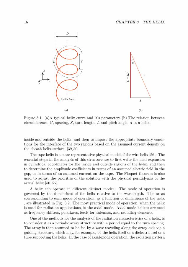
A helix is a type of smooth three-dimensional curve with the property that thetangent line at any point makes a constant angle with a fixed line called the axis.Fig. 3.1(a) shows a typical helix. Viewed end-on, a helix projects to a circle. Thediameter of this circle is called the helix diameter. The pitch or turn spacing of ahelix, S, is the height of one complete turn of the helix, measured parallel to itsaxis. If one turn of a circular helix is unrolled on a flat plane, the relation betweenthe helix diameter, pitch and length of one turn can be illustrated as in Fig. 3.1(b).The angle α is the helix pitch angle.
A realization of a helical curve can be formed by a conducting wire. A con-ducting helix is a periodic slow wave structure. This is a practical device in theelectromagnetic engineering field. It is used in low, medium and high power travel-ing wave tubes [48–50], and in low-power backward-wave oscillators [51]. The helixis particularly used in radiating structures. It is used as a highly directive broadband circularly polarized antenna [52], or as a circularly polarized feed for othertype of antennas [53–55].
3.2 Analysis of the Helix
The Helmholtz equation is not separable in a helical coordinate system [39]. Con-sequently, the solution for an electromagnetic wave propagating along a helix isusually achieved by the aid of some approximations. Two approximate models thatare mostly used to analyze the helix are to replace the actual helix with a sheathhelix or an infinitely thin conducting tape [50, 56, 57]. The sheath helix is the sim-plest model for the actual helix. This is a cylindrical tube which is assumed to haveperfect conductivity in the direction of the original winding and zero conductivityin the bi-normal direction to the direction of winding. The analysis of a sheathhelix is based on the general expansion of fields in cylindrical coordinates in regions
15
16 CHAPTER 3. THE HELIX
D
SL
Helix AxisS
L
α
C = πD
(a) (b)
z
xy
Figure 3.1: (a)A typical helix curve and it’s parameters (b) The relation betweencircumference, C, spacing, S, turn length, L and pitch angle, α in a helix.
inside and outside the helix, and then to impose the appropriate boundary condi-tions for the interface of the two regions based on the assumed current density onthe sheath helix surface. [39, 50]
The tape helix is a more representative physical model of the wire helix [56]. Theessential steps in the analysis of this structure are to first write the field expansionin cylindrical coordinates for the inside and outside regions of the helix, and thento determine the amplitude coefficients in terms of an assumed electric field in thegap, or in terms of an assumed current on the tape. The Floquet theorem is alsoused to adjust the priorities of the solution with the physical perididymis of theactual helix [50, 56].
A helix can operate in different distinct modes. The mode of operation isgoverned by the dimensions of the helix relative to the wavelength. The areascorresponding to each mode of operation, as a function of dimensions of the helix, are illustrated in Fig. 3.2. The most practical mode of operation, when the helixis used for radiation applications, is the axial mode. Axial-mode helixes are usedas frequency shifters, polarizers, feeds for antennas, and radiating elements.
One of the methods for the analysis of the radiation characteristics of a helix, isto consider it as a periodic array structure with a period equal to the turn spacing.The array is then assumed to be fed by a wave traveling along the array axis via aguiding structure, which may, for example, be the helix itself or a dielectric rod or atube supporting the helix. In the case of axial-mode operation, the radiation pattern

3.2. ANALYSIS OF THE HELIX 17
0.2 0.4 0.6 0.8 1.0 1.2 1.4 1.600
0.2
0.4
0.6
0.8
1.0
1.2
1.4
1.6
1.8
Pitch in term of wavelengths
Cir
cum
fere
nce
in te
rm o
f w
avel
engt
hs
Picth angle (deg)
60ο
45ο
15ο 30ο
75ο
90ο
Axial mode (Kraus)
Normal mode (Wheeler)
(Backfire mode)
(Normal mode)
C λ = 2√(S λ
+1)
Bifilar mode(patton)
Quadrifilar mode (Kilgus)
0
Figure 3.2: The Helix chart (reproduced from [52] under Mc-Graw Hill permissionlicence NO. ALI32138).
of the antenna can be well approximated with the Hansen–Woodyard increaseddirectivity condition for linear phase arrays [52].
18 CHAPTER 3. THE HELIX
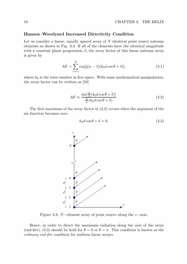
Hansen–Woodyard Increased Directivity Condition
Let us consider a linear, equally spaced array of N identical point source antennaelements as shown in Fig. 3.3. If all of the elements have the identical magnitudewith a constant phase progression, δ, the array factor of this linear antenna arrayis given by
AF =
N∑
n=1
exp[j(n− 1)(k0d cos θ + δ)], (3.1)
where k0 is the wave number in free space. With some mathematical manipulation,the array factor can be written as [58]
AF ≈ sin[ N2 (k0d cos θ + δ)]
N2 (k0d cos θ + δ)
. (3.2)
The first maximum of the array factor in (3.2) occurs when the argument of thesin function becomes zero
k0d cos θ + δ = 0. (3.3)
1
2
3
4
N
θ
θ
θ
θ
θ
z
y
d
d
d
Figure 3.3: N−element array of point source along the z−axis.
Hence, in order to direct the maximum radiation along the axis of the array(end-fire), (3.3) should be hold for θ = 0 or θ = π. This condition is known as theordinary end-fire condition for uniform linear arrays.
3.2. ANALYSIS OF THE HELIX 19
For the helix as an array of elements, the element spacing is equal to the he-lix pitch. Considering the helix as a surface wave structure, the phase differencebetween the two adjacent elements would be equal to
δ = −βs, (3.4)
where β is the phase constant of the cylindrical surface wave traveling along theaxis of the helix and s is the helix pitch.
Imposing (3.4) in (3.3) for end-fire radiation, with s = d, gives k0 = β, whichis a contradiction due to the slow wave nature of the helix. However, the axialmode end-fire radiation of the helix can be well simulated with a linear array underthe Hansen–Woodyard condition [52]. When the element spacing is small (d ≪λ), Hansen and Woodyard [59] proposed a condition for the required phase shiftbetween the adjacent elements to enhance the directivity of a uniform array withend-fire radiation. This phase shift, to have the maximum radiation intensity atθ = 0 or θ = π is given by
δ ≈ ±(k0d+ π/N). (3.5)
This requirement is known as the Hansen–Woodyard condition for end-fire radiationand leads to a larger directivity than the ordinary end-fire condition for lineararrays.


Chapter 4
Phase Velocity in Dielectric Rodsand Tubes
4.1 Introduction
It was mentioned in Section 2.1 that the dielectric tubes and rods 1 are widely usedin communication as wave guides and radiators. They are also used for supportinghelical antennas [52]. As described in Chapter 3, one of the methods used to analyzethe characteristics of a helical antenna is to consider it as an array of conductors.These conductors are fed by a traveling wave in the direction of the helix axis.It was also mentioned that the radiation pattern of a helix operating in the axialmode has a good agreement with the radiation pattern of an end-fire linear arrayunder the Hansen–Woodyard condition [52]. The important factor in this analysisis the set of characteristics of the traveling wave that feed the array elements, and,in particular, the phase velocity of this feeding wave.
In this thesis, cylindrical and ring shape (hollow cylinder) dielectric resonatorsare loaded to the helix as supporters. In the case in which a helix is supported by acircular cross section dielectric resonator, or from another perspective, a dielectricresonator that is excited by a helix, the dielectric resonator height is usually shorterthan that of the helix. In this case, the feeding wave is the surface wave travelingin the direction of the axis of the dielectric resonator. The exact analytical solutionfor a cylindrical and ring shape dielectric resonator does not exist. However, thedielectric resonator can be considered as a dielectric rod transmission line thatis terminated. The termination of a transmission does not significantly affect itscharacteristics. Hence, the solution for infinitely long dielectric rods and tubescan be used to estimate the phase velocity of a traveling surface wave along thecylindrical and ring dielectric resonators, respectively.
1In this thesis dielectric rod refers to an infinitely long circular cross section cylindrical di-electric rod. Correspondingly, dielectric tube denotes an infinite circular cross section cylindricalshell.
21
22 CHAPTER 4. PHASE VELOCITY IN DIELECTRIC RODS AND TUBES
In this chapter, the dielectric rod and tube are analytically investigated. Thehelixes do not have angular symmetry. Hence, TM or TE surface wave modes donot exist in the cylindrical dielectric supporter of the helix. In this case, the hybridmodes that are a combination of TM or TE, can exist. All of these hybrid modesexhibit a cutoff frequency with the exception of the HE11 modes that have no cutofffrequency (zero cutoff). These modes are the dominant modes in the dielectric rodsand tubes and are widely used for radiation applications [39, 45]. In the followingtwo sections, the phase velocity of the HE11 surface wave modes in a dielectric rodand tube are determined. These phase velocities are compared for different valuesof the dielectric constant in a dielectric rod and for different values of the wallthickness for the dielectric tube.
4.2 Dielectric Rods
The field component expansions for the hybrid mode for a circular dielectric rod wasexpressed in (2.7) and (2.8) for inner and outer region respectively. The coefficientAn, Bn, Cn, and Dn are related to each other by imposing the boundary conditionsat ρ = a, where a is the radius of the rod. The boundary conditions at ρ = arequire continuity of electric and magnetic field component of
E1z (ρ = a, φ, z) = E2
z (ρ = a, φ, z) (4.1)
E1φ(ρ = a, φ, z) = E2
φ(ρ = a, φ, z) (4.2)
H1z (ρ = a, φ, z) = H2
z (ρ = a, φ, z)
H1φ(ρ = a, φ, z) = H2
φ(ρ = a, φ, z)
Imposing the boundary conditions and writing the resulting equations in a ma-trix form gives
Jn(kρda) 0 −Kn(kρa) 0
− nβk2
ρdρJn(kρda) jωµ0
kρdJ ′
n(kρda) − nβk2
ρaKn(kρa) jωµ0
kρK ′
n(kρa)
0 Jn(kρda) 0 −Kn(kρa)jωεkρd
J ′n(kρda) nβ
k2
ρdaBnJn(kρda) jωε0
kρK ′
n(kρa) nβk2
ρaKn(kρa)
An
Bn
Cn
Dn
= 0
(4.3)
Equation (4.3) has a nontrivial solution for the coefficients An, Bn, Cn, andDn, provided that the determinant of the square matrix vanishes. Applying thiscondition to the square matrix in (4.3) and with some mathematical manipulationswe obtain the eigenvalue equation of a dielectric rod of relative permittivity εr andradius a as [39]

4.2. DIELECTRIC RODS 23
[
εrJ′n(u1)
u1Jn(u1)+
K ′n(u2)
u2Kn(u2)
] [
J ′n(u1)
u1Jn(u1)+
K ′n(u2)
u2Kn(u2)
]
=
[
nβ
k0
u21 + u2
2
u21u
22
]2
, (4.4)
where u1 = kρda, u2 = kρa and β2 = k20 + k2
ρ = εrk20 − k2
ρd.
Numerical Solution
Equation (4.4) is solved in Matlab for u1 and u2. It is known that u1 and u2 arerelated together as
u21 + u2
2 = (εr − 1)k20a
2 = R2, (4.5)
where R is a constant that is dependent on the relative permittivity and radiusof the dielectric rod and the free space wavenumber, k0. Equation (4.5) can bereformulated as
u1 = R sin y u2 = R cos y (4.6)
Substituting (4.6) in (4.4), gives an equation with one unknown, y. The resultingequation is solved using fminbnd command in Matlab. The relative phase velocityin terms of y is given by
v
c=k0
β=
1√
sin2 y + εr cos2 y. (4.7)
The numerical solution for the relative axial phase velocity (phase velocity alongthe axis of the cylinder) in dielectric rods with three different values of the dielectricconstant, as a function of the normalized circumference of the rod, is plotted in Fig.4.1. It can be seen that for small values of the radius the axial phase velocity in adielectric rod is close to the velocity of light, c. For very large value of the radius itconverges to the value c/
√εr. Furthermore, the slope of the curve is steeper for a
rod with a greater dielectric constant. In other words, for a given value of the radius,the relative phase velocity is smaller for rods with higher dielectric constants.
The electric field intensity for all components of the HE11 mode as well as themagnitude of the total electric field of this mode in a dielectric rod are illustratedin Fig. 4.2. The dielectric constant of the rod is εr = 10. The fields are plottedfor k0a = 0.75. Based on the solution for the phase velocity for the case εr = 10presented in Fig. 4.1, for k0a = 0.75 we have k0/β = 0.616. The fields outsidethe rod are shown for a distance equal to the radius of the rod from the outersurface of the rod. It can be observed that a good agreement exists between theapproximated field distribution of the HE11δ in a cylindrical DRA that was shownin Fig. 2.2 and the HE11 mode in a dielectric rod. The φ-component of the electricfield is maximal at the center and slowly decreases up to the surface of the rod.

24 CHAPTER 4. PHASE VELOCITY IN DIELECTRIC RODS AND TUBES
0.4 0.5 0.6 0.7 0.8 0.9 1 1.1 1.20.2
0.4
0.6
0.8
1
2πa/λ
v/c
εr = 5εr = 10εr = 20
Figure 4.1: Normalized phase velocity of the HE11 surface eave mode in dielectricrods for three different dielectric constant as a function of the normalized circum-ference of the rod.
This reduction is continued outside of the rod with a faster rate than it was in theinside region. The maximum radial component is in the outer region of the rod. Itis also high at the center and rapidly diminishes to low values at the inner surfaceof the rod. The z-component vanishes at the center. This increases to its maximumat the inner surface and slowly decreases with distance beyond the surface in theoutside region. The intensity of the total electric field is shown in Fig. 4.2(d). It isshown that the electric filed is bound to the surface of the rod in the outer region.By increasing the frequency, the field will be more tightly bound to the surface.
4.3 Dielectric Tubes
The same type of analysis as was done for dielectric rods, can be utilized for di-electric tubes. In the case of dielectric tube the analysis is more difficult than thecase of the rod as there are two boundaries to be considered, the inner and outertube surfaces, and also additional parameter, the tube wall thickness b−a, see Fig.4.3. The dielectric tube separates the space into three regions. These regions areillustrated in Fig. 4.3.
In the region 1, the free space medium inside the tube when ρ ≤ a, the solutionfor fields must represent cylindrical standing waves with oscillatory behavior. Thecylindrical functions that represent this kind of radial variations of the fields areJn, the Bessel function of the first kind, and Nn, the Bessel function of the secondkind [38]. However, since the region contains the origin, Nn should be excluded

4.3. DIELECTRIC TUBES 25
aa
(a) (b)
(d) (c)
a a
Figure 4.2: The intensity of the electric field components of the HE11 mode withe−jφ azimuthal variation, inside and outside of a dielectric rod of permittivity εr =10 on a cross sectional transverse plane. (a) |Eφ|, (b) |Eρ|, (c) |Ez | and |E|. Thefield are plotted for k0a = 0.75 that leads to k0/β = 0.616.
a
b
Region 2
x
y
εr
Region 3
Region 1
Figure 4.3: The cross section of a dielectric tube.
from the solution. Furthermore, in the tube case, the Bessel function of the firstkind Jn with imaginary argument is converted to the modified Bessel function of thefirst kind, In. The fields components in the region 1, ρ ≤ a, can then be expressedas
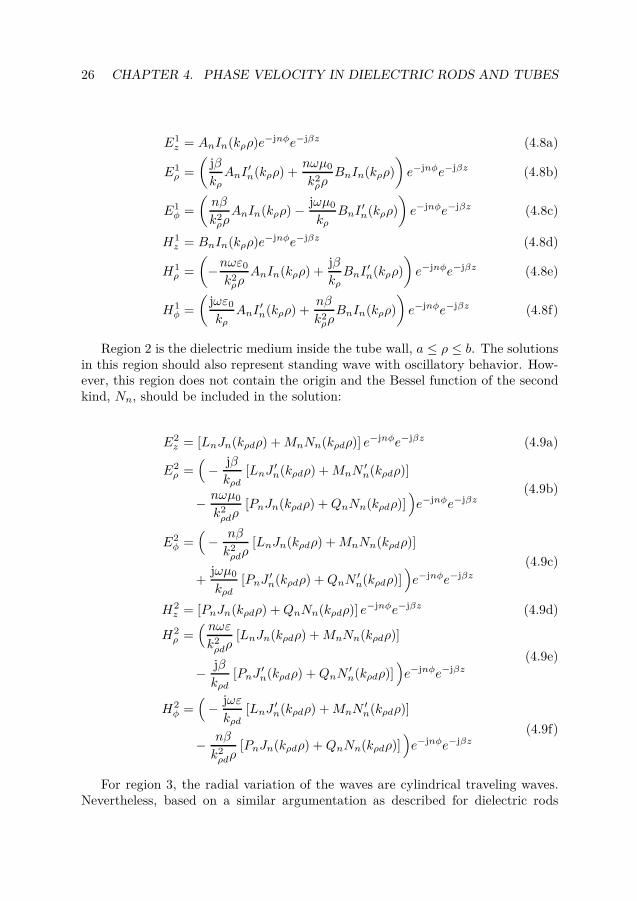
26 CHAPTER 4. PHASE VELOCITY IN DIELECTRIC RODS AND TUBES
E1z = AnIn(kρρ)e−jnφe−jβz (4.8a)
E1ρ =
(
jβ
kρAnI
′n(kρρ) +
nωµ0
k2ρρ
BnIn(kρρ)
)
e−jnφe−jβz (4.8b)
E1φ =
(
nβ
k2ρρAnIn(kρρ) − jωµ0
kρBnI
′n(kρρ)
)
e−jnφe−jβz (4.8c)
H1z = BnIn(kρρ)e−jnφe−jβz (4.8d)
H1ρ =
(
−nωε0
k2ρρ
AnIn(kρρ) +jβ
kρBnI
′n(kρρ)
)
e−jnφe−jβz (4.8e)
H1φ =
(
jωε0
kρAnI
′n(kρρ) +
nβ
k2ρρBnIn(kρρ)
)
e−jnφe−jβz (4.8f)
Region 2 is the dielectric medium inside the tube wall, a ≤ ρ ≤ b. The solutionsin this region should also represent standing wave with oscillatory behavior. How-ever, this region does not contain the origin and the Bessel function of the secondkind, Nn, should be included in the solution:
E2z = [LnJn(kρdρ) +MnNn(kρdρ)] e−jnφe−jβz (4.9a)
E2ρ =
(
− jβ
kρd[LnJ
′n(kρdρ) +MnN
′n(kρdρ)]
− nωµ0
k2ρdρ
[PnJn(kρdρ) +QnNn(kρdρ)])
e−jnφe−jβz(4.9b)
E2φ =
(
− nβ
k2ρdρ
[LnJn(kρdρ) +MnNn(kρdρ)]
+jωµ0
kρd[PnJ
′n(kρdρ) +QnN
′n(kρdρ)]
)
e−jnφe−jβz
(4.9c)
H2z = [PnJn(kρdρ) +QnNn(kρdρ)] e−jnφe−jβz (4.9d)
H2ρ =
( nωε
k2ρdρ
[LnJn(kρdρ) +MnNn(kρdρ)]
− jβ
kρd[PnJ
′n(kρdρ) +QnN
′n(kρdρ)]
)
e−jnφe−jβz(4.9e)
H2φ =
(
− jωε
kρd[LnJ
′n(kρdρ) +MnN
′n(kρdρ)]
− nβ
k2ρdρ
[PnJn(kρdρ) +QnNn(kρdρ)])
e−jnφe−jβz(4.9f)
For region 3, the radial variation of the waves are cylindrical traveling waves.Nevertheless, based on a similar argumentation as described for dielectric rods
4.3. DIELECTRIC TUBES 27
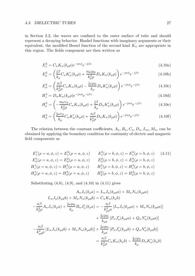
in Section 2.2, the waves are confined to the outer surface of tube and shouldrepresent a decaying behavior. Hankel functions with imaginary arguments or theirequivalent, the modified Bessel function of the second kind Kn are appropriate inthis region. The fields component are then written as
E3z = CnKn(kρρ)e−jnφe−jβz (4.10a)
E3ρ =
(
jβ
kρCnK
′n(kρρ) +
nωµ0
k2ρρ
DnKn(kρρ)
)
e−jnφe−jβz (4.10b)
E3φ =
(
nβ
k2ρρCnKn(kρρ) − jωµ0
kρDnK
′n(kρρ)
)
e−jnφe−jβz (4.10c)
H3z = DnKn(kρρ)e−jnφe−jβz (4.10d)
H3ρ =
(
−nωε0
k2ρρ
CnKn(kρρ) +jβ
kρDnK
′n(kρρ)
)
e−jnφe−jβz (4.10e)
H3φ =
(
jωε0
kρCnK
′n(kρρ) +
nβ
k2ρρDnKn(kρρ)
)
e−jnφe−jβz (4.10f)
The relation between the constant coefficients, An, Bn, Cn, Dn, Lm,Mn, can beobtained by applying the boundary condition for continuity of electric and magneticfield components as
E1z (ρ = a, φ, z) = E2
z (ρ = a, φ, z) E2z (ρ = b, φ, z) = E3
z (ρ = b, φ, z) (4.11)
E1φ(ρ = a, φ, z) = E2
φ(ρ = a, φ, z) E2φ(ρ = b, φ, z) = E3
φ(ρ = b, φ, z)
H1z (ρ = a, φ, z) = H2
z (ρ = a, φ, z) H2z (ρ = b, φ, z) = H3
z (ρ = b, φ, z)
H1φ(ρ = a, φ, z) = H2
φ(ρ = a, φ, z) H2φ(ρ = b, φ, z) = H3
φ(ρ = b, φ, z)
Substituting (4.8), (4.9), and (4.10) in (4.11) gives
AnJn(kρa) = LnJn(kρda) +MnNn(kρda)
LnJn(kρdb) +MnNn(kρdb) = CnKn(kρb)
− nβ
k2ρρAnJn(kρa) +
jωµ0
kρBnJ
′n(kρa) = − nβ
k2ρda
[LnJn(kρda) +MnNn(kρda)]
+jωµ0
kρd[PnJ
′n(kρda) +QnN
′n(kρda)]
− nβ
k2ρdρ
[LnJn(kρdb) +MnNn(kρdb)] +jωµ0
kρd[PnJ
′n(kρdb) +QnN
′n(kρdb)]
=nβ
k2ρρCnKn(kρb) − jωµ0
kρDnK
′n(kρb)
28 CHAPTER 4. PHASE VELOCITY IN DIELECTRIC RODS AND TUBES
BnJn(kρa) = PnJn(kρda) +QnNn(kρda) (4.12)
PnJn(kρdb) +QnNn(kρdb) = DnKn(kρb)
− jωε0
kρAnJ
′n(kρa) − nβ
k2ρρBnJn(kρa) = − jωε
kρd[LnJ
′n(kρda) +MnN
′n(kρda)]
− nβ
k2ρdρ
[PnJn(kρda) +QnNn(kρda)]
− jωε
kρd[LnJ
′n(kρdb) +MnN
′n(kρdb)] − nβ
k2ρdρ
[PnJn(kρdb) +QnNn(kρdb)]
=jωε0
kρCnK
′n(kρb) +
nβ
k2ρbDnKn(kρb)
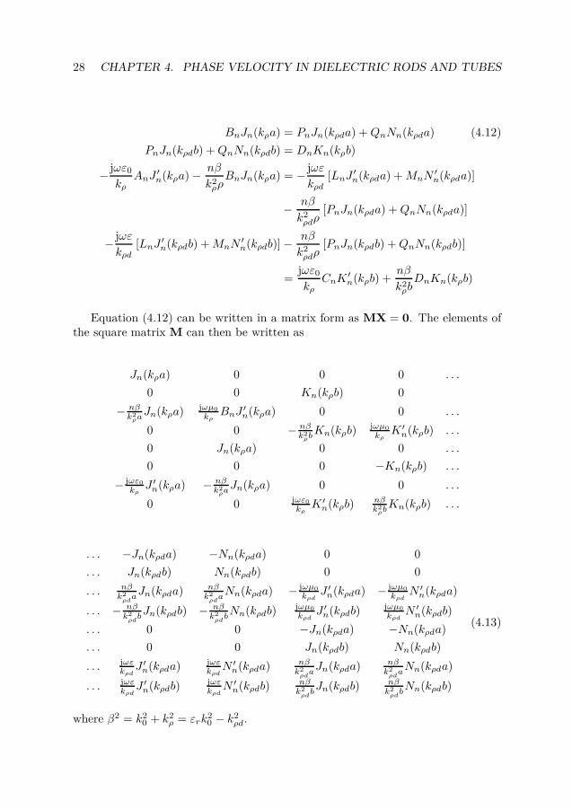
Equation (4.12) can be written in a matrix form as MX = 0. The elements ofthe square matrix M can then be written as
Jn(kρa) 0 0 0 . . .
0 0 Kn(kρb) 0
− nβk2
ρaJn(kρa) jωµ0
kρBnJ
′n(kρa) 0 0 . . .
0 0 − nβk2
ρbKn(kρb)jωµ0
kρK ′
n(kρb) . . .
0 Jn(kρa) 0 0 . . .
0 0 0 −Kn(kρb) . . .
− jωε0
kρJ ′
n(kρa) − nβk2
ρaJn(kρa) 0 0 . . .
0 0 jωε0
kρK ′
n(kρb)nβk2
ρbKn(kρb) . . .
. . . −Jn(kρda) −Nn(kρda) 0 0
. . . Jn(kρdb) Nn(kρdb) 0 0
. . . nβk2
ρdaJn(kρda) nβ
k2
ρdaNn(kρda) − jωµ0
kρdJ ′
n(kρda) − jωµ0
kρdN ′
n(kρda)
. . . − nβk2
ρdbJn(kρdb) − nβ
k2
ρdbNn(kρdb)
jωµ0
kρdJ ′
n(kρdb)jωµ0
kρdN ′
n(kρdb)
. . . 0 0 −Jn(kρda) −Nn(kρda)
. . . 0 0 Jn(kρdb) Nn(kρdb)
. . . jωεkρd
J ′n(kρda) jωε
kρdN ′
n(kρda) nβk2
ρdaJn(kρda) nβ
k2
ρdaNn(kρda)
. . . jωεkρd
J ′n(kρdb)
jωεkρd
N ′n(kρdb)
nβk2
ρdbJn(kρdb)
nβk2
ρdbNn(kρdb)
(4.13)
where β2 = k20 + k2
ρ = εrk20 − k2
ρd.
4.3. DIELECTRIC TUBES 29
The above mentioned equation represent a homogamous linear system of equa-tions. To have a nontrivial solution of such a system, the determinant of the matrixM should vanish. Equating the evaluated determinant of M to zero gives the char-acteristic equation of the dielectric tube [45]:
−n4T 4 (∆3 − ∆4)2
− (a/b)4ε2
rQ2[∆3 (∆1 − ∆9/εr) (∆8 − ∆5/εr)
−∆4 (∆7 − ∆9/εr) (∆2 − ∆5/εr)]
[∆3(∆1 − ∆9)(∆8 − ∆5) − ∆4(∆7 − ∆9)(∆2 − ∆5)]
−2n2T 2εrQ(b/a)2∆3∆4(∆1 − ∆7)(∆2 − ∆8)
+n2T 2εrQ[(∆8∆3 − ∆2∆4) − ∆5(∆3 − ∆4)]
[(∆8∆3 − ∆2∆4) − (∆5/εr)(∆3 − ∆4)]
+n2T 2εrQ(b/a)4[(∆1∆3 − ∆7∆4) − ∆9(∆3 − ∆4)]
[(∆1∆3 − ∆7∆4) − (∆9/εr)(∆3 − ∆4)] = 0
(4.14)
where
∆1 =J ′
n(kρda)
kρdaJn(kρda)∆5 = − K ′
n(kρb)
kρbKn(kρb)
∆2 =J ′
n(kρdb)
kρdbJn(kρdb)∆7 =
N ′n(kρda)
kρdaNn(kρda)
∆3 =J ′
n(kρda)
Nn(kρda)∆8 =
N ′n(kρdb)
kρdbNn(kρdb)
∆4 =Jn(kρdb)
Nn(kρdb)∆9 = − I ′
n(kρa)
kρaIn(kρa)
T = (1/kρdb)2 + (1/kρdb)
2
Q =k2
ρd + k2ρ
k2ρd + εrk2
ρ
Numerical Solution
Equation (4.14) is solved using the same method as the one described in Section4.2 for dielectric rods. The results for the relative phase velocity, v/c, versus thenormalized circumference of the tube, 2πb/λ, for the HE11 mode for tubes havingthe dielectric constant εr = 11.2 and inner to outer radii ratios a/b = 0.32, 0.5,and 0.7 are plotted in Fig. 4.4. Similar to the dielectric rods, the phase velocity oftubes with small outer radius is close to the speed of light in free space. However,it decreases with increasing outer radius. The rate of this reduction is greaterfor tubes with thicker wall. Furthermore, for a tube of given external diameterand dielectric constant, the axial phase velocity increases when the wall thicknessdecreases (a/b increases). Hence, the phase velocity in a solid rod with a/b = 0,

30 CHAPTER 4. PHASE VELOCITY IN DIELECTRIC RODS AND TUBES
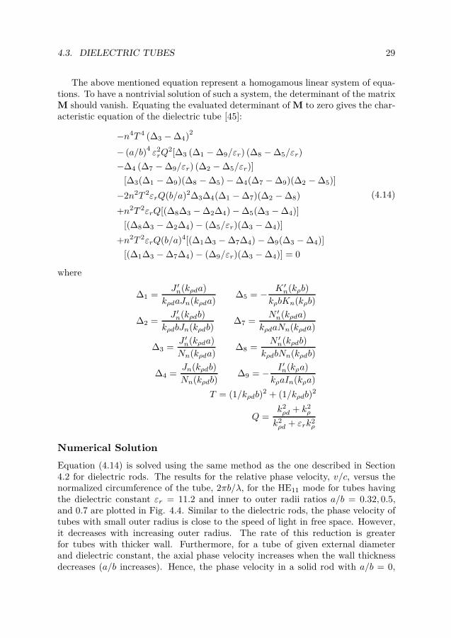
is less than the phase velocity in a tube with the same dielectric constant andouter radius as the dielectric rod. These are expected phenomena since the phasevelocity is dependent on the effective permittivity of the waveguide medium. Theless effective permittivity of the waveguide medium would support the travelingwaves with higher phase velocity. The effective permittivity for unit volume of adielectric tube decreases as the a/b ratio increases. Hence, the phase velocity ishigher for dielectric tubes with higher a/b ratio. This is also clear by comparingFig. 4.1 and 4.4.
0.6 0.7 0.8 0.9 1 1.1 1.20.4
0.6
0.8
1
2πb/λ
v/c
a/b = 0.32
a/b = .5
a/b = 0.7
Figure 4.4: Normalized phase velocity of the HE11 surface eave mode in dielectrictubes of dielectric constant εr = 11.2 and for three different inner to outer radiiratios, a/b = 0.32, 0.5 and 0.7, as a function of the normalized circumference of thetubes.

Chapter 5
Polarization of Antennas
5.1 Introduction
The polarization of an antenna in a given direction is defined as the polarizationof the fields radiated by the antenna in that direction [58]. Practically, the po-larization of the radiated wave varies with the direction of radiation with respectto the antenna. Therefore, different points of the antenna radiation pattern mayhave different polarizations. In the case that the direction is not mentioned, thepolarization is taken to be the polarization in the direction of maximum radiationintensity [58].
The polarization of an antenna is a far-field quantity where the radiated wavesby the antenna are usually approximated by plane waves. Hence, the polarizationof an antenna is the same as the polarization of the plane wave that approximatesthe radiated wave by the antenna in the far-field region.
The polarization of a time harmonic uniform plane wave describes the timevarying behavior of the electric field intensity vector over one period of oscillationat a given point in space [60]. The polarization of an electromagnetic field isimportant in many practical applications, such as [61]
• For the purpose of optimizing the propagation through a selective medium(such as the ionosphere) or optimizing the back scattering off a target. Thisplaces a constraint on the design of a transmitting antenna.
• The polarization of an incoming wave may have to be accepted (which placesa constraint on the design of the receiving antenna that will receive this waveoptimally).
• The polarization of an incoming wave may be unpredictable (it is desirablein this case to design a receiving antenna which will respond equally to allpolarizations).
31

32 CHAPTER 5. POLARIZATION OF ANTENNAS
In order to deal with problems similar to that mentioned above, it is necessaryto define, describe, and quantify the polarization of an electromagnetic wave.
5.2 Linear, Circular, and Elliptical Polarizations
There are in general two types of antennas: Type I antennas of which the actualcurrent distribution is well known like dipoles and helices. Type II antennas arethose for which the actual current distribution is difficult to deduce, but they couldbe enclosed by a surface over which the fields are known with reasonable accuracy,such as horns and slots. In either case, the far field pattern of a transmittingantenna can be viewed as the product of an outgoing spherical wave in a complexdirectional weighting function [61]. The electric field at a far-field distance can berepresented by
E = (aθEθ + aφEφ) ejωt, (5.1)
for time harmonic sources.
The functions Eθ(r, θ, φ) and Eφ(r, θ, φ) are in general complex:
Eθ = E′θ + jE′′
θ (5.2)
Eφ = E′φ + jE′′
φ . (5.3)
The instantaneous field can then be written as
E (r, θ, φ, t) = ℜ[E] = aθ(E′θ cosωt− E′′
θ sinωt) + aφ(E′φ cosωt− E′′
φ sinωt), (5.4)
where E′θ, E′′
θ , E′φ, and E′′
φ are real valued functions of the spherical coordinates,r, θ, and φ.
Equation (5.4) can be written in the form
E (r, θ, φ, t) = aθA cos(ωt+ α) + aφB cos(ωt+ β), (5.5)
in which
A =√
(E′θ)2 + (E′′
θ )2 B =√
(E′φ)2 + (E′′
φ)2
α = arctanE′′
θ
E′θ
β = arctanE′′
φ
E′φ
. (5.6)
With no loss in generality, the origin of time can be chosen such that α = 0.Hence, (5.5) can be written as
E (r, θ, φ, t) = aθA cosωt+ aφB cos(ωt+ β). (5.7)
5.3. THE AXIAL RATIO 33
In general, the polarization of an electromagnetic wave is elliptical. This meansthe curve traced by the end point of the electric field vector arrow, at a givenposition, as a function of time, is an ellipse. Two important specific cases of ellipticalpolarization are linear polarization and circular polarization. An electromagneticwave is said to be linearly polarized when
β = nπ, n = 1, 2, 3, . . . (5.8)
Linear polarization is that specific type of elliptical polarization when the minoraxis of the ellipse is zero. Anther specific situation occurs when
A = B, & β = ±(n+1
2)π, (5.9)
which is known as circular polarization condition. This is also a particular case ofelliptical polarization: when the major and minor axis of the ellipse are equal.
5.3 The Axial Ratio
It was mentioned in Section 5.2 that the most general case for the polarization of aplane wave is elliptical polarization. In this case, the curve traced by the end pointof the electric field vector at a given position as a function of time is a tilted ellipse.The ratio of the major axis to the minor axis of the polarization ellipse is referredto as the axial ratio (AR).
Based on (5.7), the magnitude of the instantaneous electric field is given by:
|E (r, θ, φ, t)| =[
A2 cos2 ωt+B2 cos2(ωt+ β)]1/2
. (5.10)
If the time derivative of this function is set equal to zero, the maximum andminimum of |E (r, θ, φ, t)| can be identified. They occur at angles ωt = τ governedby
tan 2τ = − B2 sin 2β
A2 +B2 cos 2β. (5.11)
If the first and second solutions of (5.11) are τ1 and τ2, then |τ1 − τ2| = π/2.This means that the direction of maximum and minimum magnitude of the electricfield are at right angles to each other. This is to be expected since they are indeedthe principal axes of the ellipse traced by the electric field vector. The magnitudesof semi-major and semi-minor axes can be found by substituting τ1 and τ2 into(5.10). This gives [61]
|E | =
[
A2 +B2
2±(
B2
2
)
sin 2β
sin 2τ1
]1/2
. (5.12)
34 CHAPTER 5. POLARIZATION OF ANTENNAS
Equation (5.7) indicates that, excluding linear polarization as an exceptionalcase, |E (r, θ, φ, t)| rotates at a uniform rate with an angular velocity ω in the θ−φplane. If the fingers of the right hand follow the direction of the rotation and thethumb points to the direction of propagation, the wave is right hand ellipticallypolarized. Otherwise, if the direction of rotation of |E | and propagation of thewave followed by the fingers and thumb of the left hand, the wave is left handelliptically polarized. The same categorization exists for circularly polarized waves.
The axial-ratio of a plane wave can be determined using (5.12). This quantityis often measured in dB as
AR = 20 log
( |E |max
|E |min
)
(5.13)
The AR equals 0 dB for a circularly polarized wave and is infinite for a linearlypolarized wave. However, an axial ratio less than or equal to 3 dB is usuallyconsidered as accruable value when a circularly polarized wave is required [37].
Circularly polarized antennas are preferred in various communication systems.This is due to the advantages provided by them as compared to linearly polarizedantennas, such as greater flexibility in the orientation between the transmitter andreceiver antennas and less sensitivity to propagation effects [62].
A circularly polarized wave can be synthesized from two spatially orthogonal lin-early polarized waves that are in phase quadrature (±π/2 phase offset). An antennacapable of generating two linearly polarized wave that are spatially orthogonal andin phase quadrature will therefore generate a circularly polarized radiation.

Chapter 6
Results
In the first part of this thesis, a novel excitation technique for cylindrical dielectricresonator antennas is introduced to produce circular polarization. The exciter isa tape helix that is wound around the dielectric resonator and is fed by a coax-ial probe. The geometry of the proposed antenna is illustrated in Fig. 6.1. Theproposed architecture is a combination of two basic antenna structures, a helicalantenna and a dielectric resonator antenna. Therefore, this new class of antennaoffers characteristics that are shared between helical antennas and DRAs. Theproposed antenna is more than regular unloaded helix antenna. The antenna band-width is wider than basic cylindrical DRAs and is also circularly polarized. Thischaracteristic drives from the wide band circularly polarized nature of the helix tothe DRA.
The operation of this class of antenna can be viewed in a more systematic way.As explained in Section 2.3, an external helix wound around a cylindrical DRA canbe an efficient tool to excite the HE11δ mode in a DRA. Furthermore, the helix iscapable of exciting both of these modes that are in phase quadrature, due to itsazimuthal symmetry. This leads to a circularly polarized radiation. As comparedwith other single feed cylindrical DRAs, the proposed antenna provides a broader3 dB axial-ratio bandwidth.
The helix is naturally a wide band radiating structure. The band width of theproposed type of antenna is mainly restricted by the DRA rather than the helix.Hence, in order to enhance the antenna bandwidth, the bandwidth of the DRAshould be enhanced. Some of the methods used to enhance the bandwidth of thecylindrical DRAs can also be employed to develop the proposed class of antenna.Among these techniques, removing the central portion of the dielectric cylinder tocreate a dielectric ring and also utilizing stacked cylindrical DRAs are investigatedin this thesis. They both are shown to perform well in the impedance and 3 dBaxial-ratio bandwidths enhancement of the proposed type of antenna.
35

36 CHAPTER 6. RESULTS
y
z
x
Ground Plane
Probe
l
h
a
Figure 6.1: The configuration of a cylindrical DRA excited by a helix.
6.1 Design
In the proposed class of antenna, the helix excites the HE11δ modes in the cylindricalDRA. The resonance frequency of the antenna structure can be estimated from thegeneral formula for HE11δ modes in a cylindrical DRA [62],
2πa
λr= 2.735ε−0.436
r [0.543 + 0.589x− 0.050x2], (6.1)
where x = a/2h and λr is the wavelength at the resonant frequency in free space.
The proposed antenna is a hybrid antenna that consists of two classic radiatingarchitectures: a helical antenna and a DRA. In order for the antenna to functionproperly, the two elements are required to have similar radiation characteristics. Atypical radiation pattern of the HE11δ modes in a cylindrical DRA is shown in Fig.6.2(a). Typical radiation patterns for normal mode and axial mode helix antennaare also illustrated in Fig. 6.2 (b) and (c) respectively. It can be observed that theradiation pattern of the HE11δ modes DRA and axial mode helix are broad-side,while for the normal mode helix the pattern is omnidirectional. Hence, in orderfor the antenna to function properly, the helix is required to operate in its axialmode to be compatible with the radiation characteristics of the HE11δ modes. Asmentioned in Chapter 3, the radiation pattern for the axial mode helix antenna canbe well approximated with the Hansen–Woodyard increased directivity conditionfor linear phase arrays. The Hansen–Woodyard condition (3.5) for the helix in Fig.6.1, considering the image theorem with respect to the conducting ground planecan be written as
6.1. DESIGN 37
2l
πa
[ c
v− 1]
=λ
2πa, (6.2)
where λ is the wavelength in free space, c is the free space phase velocity, and v isthe surface wave phase velocity along the z axis.
The phase velocity, v, is the HE11δ mode surface wave phase velocity along theside wall of the DRA. This phase velocity can be estimated from the axial phaseconstant of the HE11 surface wave mode in an infinite dielectric rod with the samepermittivity and radius as the dielectric resonator. The solution for the phaseconstant in a dielectric rod was discussed in Section 4.2.
(a) (b) (c)
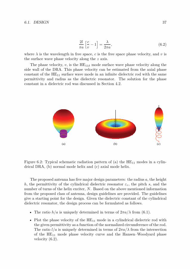
Figure 6.2: Typical schematic radiation pattern of (a) the HE11 modes in a cylin-drical DRA, (b) normal mode helix and (c) axial mode helix.
The proposed antenna has five major design parameters: the radius a, the heighth, the permittivity of the cylindrical dielectric resonator εr, the pitch s, and thenumber of turns of the helix exciter, N . Based on the above mentioned informationfrom the proposed class of antenna, design guidelines are provided. The guidelinesgive a starting point for the design. Given the dielectric constant of the cylindricaldielectric resonator, the design process can be formulated as follows.
• The ratio h/a is uniquely determined in terms of 2πa/λ from (6.1).
• Plot the phase velocity of the HE11 mode in a cylindrical dielectric rod withthe given permittivity as a function of the normalized circumference of the rod.The ratio l/a is uniquely determined in terms of 2πa/λ from the intersectionof the HE11 mode phase velocity curve and the Hansen–Woodyard phasevelocity (6.2).

38 CHAPTER 6. RESULTS
• Choose a value for 2πa/λ close to the upper bound of the helix axial mode(seeFig. 6.4). 1
• Find the corresponding value for l/a at the chosen 2πa/λ.
• From the chosen l/a, go down towards the 2πa/λ axis by the amount ∆C 2 .At this new point find the corresponding value for h/a.
The total height of the helix depends on the probe height, the pitch angle andthe number of turns. Our investigations indicate that the probe height should beas short as possible. The best values for the number of turns in the helix are withinthe interval 5.5 ≤ N ≤ 8.5. However, the most repeated optimized value for thenumber of turn is N = 8. The pitch angles can then be adjusted when the totalheight and the number of turns are known.
The design guideline is provided for the normalized DRA radius a/λ. For adesired operation frequency, the physical dimension of the radius can be determined.
This guidelines is followed here to find a starting point for the deign of threeantennas of the proposed type with three different dielectric constants. The startingpoints are then optimized for the widest 3 dB axial-ratio bandwidth using HFSS.The normalized phase velocities of the HE11 surface wave mode on infinite rodof permittivities εr = 5, 10 and 20 are plotted in Fig. 6.3, as functions of thenormalized circumference of the rods. The normalized phase velocities for theHansen–Woodyard condition with the optimized value of a/l for each case arealso plotted. It can be observed that for lower dielectric constants a larger DRAradius and taller helix height are needed for the Hansen–Woodyard condition tointersect with the HE11 mode curve in the proper region. The values for h/a andl/a determined from (6.1) and matching phase velocities of HE11 and the Hansen–Woodyard condition respectively, are plotted as a function of 2π/a for εr = 10. Thered and black circles show the optimized values for l/a and h/a respectively. Thedistance ∆C = 0.9(2πa/λw) for the optimized points. The coefficient 0.9 agreeswell with the rule of thumb mentioned in the guidelines, corresponding to one-halfof the impedance bandwidth. The values are scaled to operate at f ∼ 2.8 GHz. Theoptimized parameter values of the three designs and the resulting 3 dB axial-ratioand impedance bandwidth for each case are summarized in Table 6.1. As listed in
1It should be noted that this upper bound for an unloaded helical antenna is roughly 2πa/λ ∼
1.3. However, our case studies indicate that this value shifts downwards if the helix is loadedwith a dielectric core. The amount of this shift is proportional to the guided wavelength in thedielectric supporter of the helix. When putting a dielectric resonator with permittivity εr ∼ 10at the launching point of the helix, this upper bound reduces to 2πa/λ ∼ 0.9. The upper boundfor εr ∼ 20 is 2πa/λ ∼ 0.6.
2The percentage ∆C is supposed to be equal to one-half of the antenna band width. Theproposed antenna bandwidth for a cylindrical DRA with dielectric constant εr ∼ 10 is on theorder of 16%. The quality factor of the HE11δ in a cylindrical DRA varies with the dielectricconstant of the DRA as ε1.202
r . The bandwidth variation with the the dielectric constant of theDRA can then be well estimated as ε−1.202
r

6.1. DESIGN 39
the table, the antenna with lower dielectric constant provides a wider impedanceand 3 dB axial-ratio bandwidth.
0.3 0.4 0.5 0.6 0.7 0.8 0.9 1 1.1 1.2 1.3 1.4 1.50.2
0.3
0.4
0.5
0.6
0.7
0.8
0.9
1
v/c
εr = 5, l/a = 6.06
εr = 10, l/a = 2.00
εr = 20, l/a = 1.66
2πa/λ
HE11
mode
Hansen - Woodyard
Figure 6.3: The normalized phase velocity of the HE11 modes on infinite dielectricrod of three different values for dielectric constant together with the normalizedphase velocities of the Hansen–Woodyard condition for DRA designs with the samepermittivity as used for the rods.
Case # 1 Case # 2 Case # 3εr (mm) 5 10 20a (mm) 16 13 10h (mm) 60 18 12.2l (mm) 9.7 25.8 16.6N 8 8 7.8
s (mm) 12 3.1 2.0fr (GHz) 2.7 2.8 2.8fw (GHz) 2.98 3.0 2.9
fl − fh (GHz) 2.1–3.3 2.6–3.04 2.89–3.05Impedance BW 44 % 15.6 % 4.4 %Axial Ratio BW 28 % 6.4 % 2.9 %
Table 6.1: Design parameters and corresponding simulation results three designcases for 3 antennas of the proposed type with cylindrical DRA.
Similar design guidelines as discussed for the cylindrical DRAs can be followed todesign the proposed type of antenna using a ring DRA. However, in the case of ringDRA, in addition to the dielectric constant, the inner to outer radius ratio is also

40 CHAPTER 6. RESULTS
0.7 0.8 0.9 1 1.11
1.5
2
2.5
3
2π a/λ
h/a
0.7 0.8 0.9 1 1.11
1.5
2
2.5
3
l/a
∆C
2π a/λr
2πa/λw
Figure 6.4: The schematic illustration of the design guidelines for the case #1. Thenon-right apexes of the triangle in the figure show the optimized values for l/a andh/a.
required to start the design process. For the ring DRA, the dielectric constant εr inthe resonance frequency formula (6.1) must be replaced by the effective permittivityof ring DRA, which can be estimated by
εreff =
(
a2 − b2)
εr + b2
a2, (6.3)
where εr, a, and b are the dielectric constant, the outer radius of the ring and theinner radius of the ring, respectively.
The phase velocity, v, in (6.2) for the ring DRA case can be estimated from theaxial phase constant of the HE11 surface wave mode in an infinite dielectric tubewith similar permittivity, inner and outer radii as the corresponding ring dielectricresonator. The solution process for the phase constant of a dielectric tube wasexplained in Section 4.3 and the numerical results were also plotted in Fig. 4.4.These plots refer to tubes of permittivity εr and inner to outer radius ratios ofa/b = 3.2, 0.7 and 0.5. Three antennas of the proposed type are designed usingdielectric rings of the dielectric constant and inner to outer ratio as of the tubesreported in Fig. 4.4. The outer radii for all cases are the same and equal tob = 8.25 mm. The curves of Fig. 4.4 are again shown here in Fig. 6.5, this timetogether with the normalized phase velocities for the Hansen–Woodyard conditionwith the optimize value of l/a for each of the designed antenna case. It can beobserved that for greater a/b, a taller helix height is required for the Hansen–Woodyard condition to intersect with the HE11 mode curve in the proper region.The optimized parameter values of the three designs and the resulting 3 dB axial-ratio and impedance bandwidth for each case are summarized in Table 6.1. As
6.1. DESIGN 41
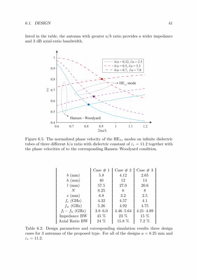
listed in the table, the antenna with greater a/b ratio provides a wider impedanceand 3 dB axial-ratio bandwidth.
0.6 0.7 0.8 0.9 1 1.1 1.20.4
0.5
0.6
0.7
0.8
0.9
1
v/c
b/a = 0.32, l/a = 2.5b/a = 0.5, l/a = 3.3b/a = 0.7, l/a = 7.0
HE11
mode
Hansen - Woodyard
2πa/λ
Figure 6.5: The normalized phase velocity of the HE11 modes on infinite dielectrictubes of three different b/a ratio with dielectric constant of εr = 11.2 together withthe phase velocities of to the corresponding Hansen–Woodyard condition.
Case # 1 Case # 2 Case # 3b (mm) 5.8 4.12 2.65h (mm) 40 12 14l (mm) 57.5 27.0 20.6N 8.25 8 8
s (mm) 6.8 3.2 2.5fr (GHz) 4.32 4.57 4.1fw (GHz) 5.26 4.92 4.75
fl − fh (GHz) 3.8–6.0 4.46–5.64 4.21–4.89Impedance BW 45 % 23 % 15 %Axial Ratio BW 24 % 15.8 % 7.2 %
Table 6.2: Design parameters and corresponding simulation results three designcases for 3 antennas of the proposed type. For all of the designs a = 8.25 mm andεr = 11.2.
42 CHAPTER 6. RESULTS
6.2 Fabrication and Measurement
For both the cylindrical and ring (hollow cylindrical) cases, prototypes were fab-ricated and measured. The dielectric resonators were purchased from T-ceramcompany. The height of the DRA and helix exciter are specified by different phe-nomena. The height of the DRA, h, is obtained from its resonance condition whilefor the helix exciter, the total height, l, is given by the Hansen–Woodyard condition.Since the radius of the DRA is restricted to be in the helix axial mode interval,this usually ends being to a greater height for the helix rather than the DRA. Inorder to support the tape helix on the top of the DRA, a Rohacell foam materialfrom Evonik was used. The dielectric constant of the Rohacell foam is 1.04, whichis very close to the free space permittivity. The cylindrical shape supporters withthe required sizes were cut out from a Rohacell fiber using scraped metallic pipesof the proper diameter as shown in Fig. 6.6(a). Fig. 6.6(b) shows some of the di-electric resonator as well as cylindrical cuts of Rohacell foam. The helical excitersin the fabricated prototypes are made out of a copper tape. A narrow strip wasclipped out from a copper tape using a double blade razor as shown in Fig. 6.6(c).Superglue was used to attach the Rohacell foam on top of the ceramic dielectricresonator and also to stick the ceramic dielectric resonator on the copper groundplane. One of the fabricated prototypes is shown in Fig. 6.7(a).
The return loss of the fabricated antennas was measured by an Anritsu MS2026Bseries network analyzer. For measurement of the far-field parameters a horn trans-mitter antenna was used. A robot positioner was employed to sweep over theazimuth, φ, and elevation, θ, angles. The antenna was mounted on the robot asshown Fig. 6.7(b). For the radiation pattern measurement the antenna was rotatedaround x or y axis with θ = 2 precision. The measured data were recorded onthe network analyzer and then synthesized by a MATLAB program to produce theradiation pattern of the antenna.
The axial ratio measurement is more complicated. As explained in Section5.3, the axial ratio (AR) is defined as the ratio of the major axis to the minoraxis of the elliptical curve traced by the end point of the electric field vector. Todetect the ellipse that is traced by the electric field, the antenna was rotated onthe robot around the z axis and measured and recorded the fields at each point.The recorded points should ideally be located on an ellipse. However, because ofnoise and imperfect experimental instruments they have offset. In order to detectthe most likely elliptical curve representing the electric field rotation a root meansquare optimization process was employed. The ratio of the major and minor axesof the detected ellipse gives an estimate for the measured AR of the antenna. Forthe cylindrical DRA case the simulation and measured results for the return lossand the axial ratio are shown in Fig. 6.8 and 6.9, respectively. It can be observedthat the measured and simulation results are in good agreement. The detailedresults for both of the fabricated antennas can be found in Papers I and II.

6.2. FABRICATION AND MEASUREMENT 43
(a)
(b)
(c)
Figure 6.6: (a) Rohacell fibre and the pipe used for cutting cylindrical pieces, (b)Cylindrical ceramic resonators and foam cuts, (c) Double blade employed to clip anarrow strip out of a copper tape.

44 CHAPTER 6. RESULTS
(a)
(b)
Figure 6.7: (a) Fabricated antenna and (b) The fabricated antenna on a robot forthe axial ratio and radiation pattern measurement
6.3 Contribution
In this thesis a new class of hybrid antenna, consisting of a helix and a dielectricresonator antenna, was introduced. Although the helix loaded dielectric core is nota new subject, there are, as far as the author knows, no systematic investigationon the design process, limitations and advantages together with a modal study onthe dielectric core in the literature on this type of antenna.
Previously, similar problems on helix loaded dielectric have been investigated.

6.3. CONTRIBUTION 45
3 3.1 3.2 3.3 3.4 3.5 3.6 3.7
−20
−10
0
Frequency (GHz)
S1
1(d
B)
MeasurementSimulation
Figure 6.8: Simulation and measurement results for reflection coefficient of the helixfed cylindrical DRA
3 3.1 3.2 3.3 3.4 3.5 3.6 3.70
3
6
9
12
Frequency (GHz)
Axia
lR
ati
o(d
B)
MeasurementSimulation
Figure 6.9: Simulation and measurement results for the axial-ratio of the helix fedcylindrical DRA
In [63], a moment method is used to analyze a helical antenna loaded by a dielectricresonator. In that paper, the helix does not touch the dielectric resonator coreand the effects due to the existence of a dielectric core and its distance from theground plane on a helical antenna parameters is studied. However, the authors didnot provide any optimal design for a dielectric loaded helix. That paper mostlyconcentrates on the solution method rather than the design performance.
A reduced size helical antenna is presented in [64]. In this work, a bi-filar helix
46 CHAPTER 6. RESULTS
is introduced that is operating in the backfire mode. Two matching strips are usedto improve the impedance bandwidth. Although a dielectric supporter is used toreduce the helix size, there is no relation provided between the reduced size andthe characteristic of the dielectric supporter.
The radiation characteristics of an axial mode helix loaded with a dielectriccore is considered in [65]. A network model is used to model the antenna as asurface wave structure. A dielectric core is included to decrease the cross polarizedradiation in the off-axis directions.
In all of the above-mentioned papers, the resonance condition of the dielectricresonator cores are not included in the design, probably due to their wide-bandnature related to their low permittivity. Furthermore, none of them provides arelation between the supporting dielectric core and the height of the helix. In [63],the authors introduce the helix as a useful exciting element for a dielectric rodantenna and comment on the excited modes in the dielectric rod. However, theheight of the rod in that paper is much longer than the helix and the dielectricconstant is also low. Also, in this case, the resonance condition of the dielectricrod is ignored, possibly due to the wide-band nature of the low dielectric constantsupporter. Moreover, there is no ground plane included in this traveling waveantenna structure.
In this thesis, we provide an approach to estimate the height of the helix as afunction of the dielectric core characteristics located at the launching point of thehelix. The approach is based on the phase velocity of the surface wave travelingalong the side wall of the dielectric resonator core. This phase velocity is estimatedfrom the solution of a dielectric rod with the permittivity and radius as the dielectricresonator core. From a dielectric resonator antenna point of view, the proposedantenna is a single point feed cylindrical DRA that provides a larger 3 dB axial ratiobandwidth as compared to the other reported single point feed antennas [37,66,67].Several antennas of this type are designed and some of them are reported in PaperI. The proposed helical type of excitation can also be used to excite circularlypolarized surface waves on other types of dielectric resonator antennas, such as fora ring (hollow cylindrical) DRA. A ring DRA supports surface waves with higherphase velocity than a similar cylindrical DRA. This leads to a size enlargement inthe DRA but at the same time an increase in the impedance and the 3 dB axial-ratiobandwidth of the antenna. This phenomenon is discussed in Paper II.
6.4 Conclusion
In the first part of this thesis a novel excitation method was introduced for cylin-drical dielectric resonator antennas. The proposed type of antenna produces acircularly polarized radiation. The exciter of the antenna is a tape helix that iswound around the dielectric resonator and is fed by a coaxial probe. As comparedto other single feed DRAs, the proposed method offers a wider impedance and 3 dBaxial-ratio bandwidths. The circularly polarized wave produced by the antenna is

6.4. CONCLUSION 47
the outcome of the excitation of two orthogonal HE11δ surface wave modes in phasequadrature in the cylindrical DRA. Design guidelines were provided and employedto create several design cases of the proposed type of antenna. The design guidelinesare based on the phase velocity of the single traveling surface along the side wallof the DRA together with the Hansen–Woodyard increased directivity conditiontogether with the general formula for the resonance frequency of the HE11δ modein cylindrical DRAs. Initial values of the design parameters were estimated usingthe presented design guidelines. The optimal values for the parameters were thenfound using HFSS. One of the simulated design examples has been fabricated andagreed well with the simulation results. The helix was also used to excite HE11δ
modes in ring DRAs. As compared with a cylindrical DRA, using the ring leadsto a wider impedance and 3 dB axial-ratio bandwidth and at the same time theantenna requires a taller helix exciter to function properly.
The proposed antenna is compact, uncomplicated, low cost, and easy to fabri-cate. The invention of this antenna can be the basis of several interesting researchproblems. Many ideas for improving cylindrical DRAs can also be used in this typeof hybrid antenna. We used two methods for bandwidth enhancement: stacking andremoving the central portion of the cylindrical DRA, in this thesis. Terminatingthe helix with a spiral strip on the top of the cylindrical DRA, using a bi-filar helix,more investigation on the effects of the pitch angle, using conical shape DRAs, theeffects of tapering of the helix, and many interesting ideas in antenna design can beapplied to this type of antenna as a single element. The proposed type of antennacan also be used and investigated as an array element.

Part II
General Introduction to APolarization Sensitive Rasorber
Design
49


Chapter 7
Statement of the Problem
7.1 Background
Reducing radar visibility is a factor in the survivability of military targets. As aconsequence, stealth or invisibility to radar is of widespread interest to researchers[68, 69]. A common method to reduce the radar signature of a target is to protectthe target with radar absorbing materials. As is implied from the name, radarabsorbing materials reduce the reflected power back to the radar receiver antennaby means of absorption of the electromagnetic energy.
For some applications, such as protecting an antenna from detection by theradar waves by a radome, the radar absorber is required to absorb electromagneticwaves at the radar detecting waves while being transparent for the frequencies atwhich the protected antenna operates. Such structures are called absorbers withwindows. They are also known as Rasorbers [70] that is a combination of wordsradome and absorber.
It is common to divide absorbers into two classes: magnetic absorbers and elec-tric absorbers. In both cases a lossy electric or magnetic sheet is placed at thelocation of the maximum electric or magnetic field respectively. In the case ofreducing the reflection from a perfect electric conductor (PEC) surface the maxi-mum electric field occurs at a quarter of a wavelength away from the PEC surfacewhile the magnetic field has its maximum on the PEC surface. Therefore, for anelectric absorber, a screen having a matched resistivity is positioned a quarter ofa wavelength apart in front of the metallic plate. These designs are often referredto as Salisbury screens [71]. A magnetic lossy sheet can be placed directly ontothe PEC surface. A consequence of the absorber lossy sheet position is that a Sal-isbury absorber is thicker than a magnetic absorber. Furthermore, the Salisburyabsorbers are efficient only for a narrow frequency band because of their resonantnature. However, the magnetic absorbers are often heavy and fragile [72], makingthem inappropriate for flying structures. Furthermore, it is difficult to find materi-als that meet particular desired conditions and they often have a strong frequency
51

52 CHAPTER 7. STATEMENT OF THE PROBLEM
variation [73]. Another complication is that the magnetic lossy sheet must haveenough low intrinsic impedance to let the incident radiation penetrate so that theconductor will be effective at establishing a boundary condition that positions themaximum magnetic field within the lossy sheet.
There are ongoing research efforts to overcome problems with magnetic ab-sorbers, see, e.g., [72, 74, 75]. The bandwidth of a Salisbury screen can be im-proved by adding extra resistive sheets and dielectric spacers to form a Jaumannabsorber [71, 73]. The reason for this improvement is to create an extra resonancein the screen structure which increases the bandwidth of efficient absorption.
The main blocking part of Salisbury and Jaumann absorbers is the PEC backingsurface. Hence, the first step to introduce a transparent window in a conventionalabsorber is to replace the PEC surface with a structure that is as transparentas possible for the waves of the transparent window frequency while providing aPEC-like behavior for the other frequencies, to enable the absorption phenomenon.
7.2 Design Goals
The subject of this part of the thesis is to design a rasorber with different require-ments for two orthogonal linear polarizations. The rasorber is required to have atransparent window at 1 GHz for one of the polarizations and provide as muchabsorption as possible for the other frequencies in the band of interest with thispolarization and also for all frequencies in this band with the other polarization.The frequency band of interest in this problem is 1–20 GHz.
Several constraints should be considered in the design process, such as the widestpossible -20 dB absorption bandwidth, the highest transmission coefficient and thelowest loss at the transparent window, and also the smallest structure thickness.
In the next chapter, the theories and tools that have been used in the rsorberdesign process will be briefly presented.

Chapter 8
Analysis of Stratified PeriodicStructures
In order to design the rasorbers presented in this thesis, two approaches were used inparallel: a wave splinting method and a full wave simulation using HFSS commercialsoftware. The wave splitting method provides a fast approach to optimize therasorber as a stratified structure. The full wave HFSS simulations were used toverify the results and also to synthesize the approximate model given by the wavesplitting method. In this chapter, a brief description of these methods as appliedto planar stratified structures will be presented.
8.1 Wave Splitting Method for the Analysis of StratifiedStructures
The major part of the investigations in the second part of this thesis is on planarstratified structures. In the case of rasorber design, the parameters of the struc-ture are optimized for the required reflection and transmission coefficients over awide frequency band. The full-wave analysis of a planar structure for such a mul-tidimensional optimization in a scattering problem for a wide frequency band canbe computationally intensive and time consuming. For these problems it is moreconvenient to use an approximate method to reduce the computation time of theoptimization problem.
In this chapter, a wave splitting technique [73, 76–78] will be introduced. Thisapproach is based on assuming a certain form of the electric and magnetic fieldson both sides of the impedance boundary in the dielectric layers of a stratifiedstructure and on specifying the required boundary conditions that the fields mustsatisfy. This technique provides a fast method to obtain the transmission andreflection coefficients as functions of the boundary impedances and layer thicknessof a normally illuminated stratified structure.
53
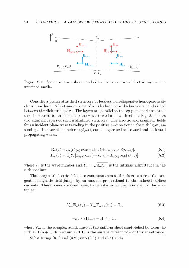
54 CHAPTER 8. ANALYSIS OF STRATIFIED PERIODIC STRUCTURES
Er n( )
Ei n( )
Hi n( )
Hr n( )
Er n( +1)
Ei n+( 1)
Hi n( +1)
Hr n( +1)
Ysn
z=zn
(εn , µ
n)(ε
n+1 , µ
n+1)
z
x
Figure 8.1: An impedance sheet sandwiched between two dielectric layers in astratified media.
Consider a planar stratified structure of lossless, non-dispersive homogenous di-electric medium. Admittance sheets of an idealized zero thickness are sandwichedbetween the dielectric layers. The layers are parallel to the xy-plane and the struc-ture is exposed to an incident plane wave traveling in z direction. Fig. 8.1 showstwo adjacent layers of such a stratified structure. The electric and magnetic fieldsfor an incident plane wave traveling in the positive z−direction in the n:th layer, as-suming a time variation factor exp(jωt), can be expressed as forward and backwardpropagating waves:
En(z) = ax[Ei(n) exp(−jknz) + Er(n) exp(jknz)], (8.1)
Hn(z) = ayYn[Ei(n) exp(−jknz) − Er(n) exp(jknz)], (8.2)
where kn is the wave number and Yn =√
εn/µn is the intrinsic admittance in then:th medium.
The tangential electric fields are continuous across the sheet, whereas the tan-gential magnetic field jumps by an amount proportional to the induced surfacecurrents. These boundary conditions, to be satisfied at the interface, can be writ-ten as
YsnEn(zn) = YsnEn+1(zn) = Js, (8.3)
−az × (Hn−1 − Hn) = Js, (8.4)
where Ysn is the complex admittance of the uniform sheet sandwiched between then:th and (n+ 1):th medium and Js is the surface current flow of this admittance.
Substituting (8.1) and (8.2), into (8.3) and (8.4) gives

8.1. WAVE SPLITTING METHOD FOR THE ANALYSIS OF STRATIFIEDSTRUCTURES 55
Ei(n+1) =exp(jkn+1zn)
2Yn+1[(Yn+1 + Yn + Ysn)Ei(n) exp(−jknzn)
+(Yn+1 − Yn + Ysn)Er(n) exp(jknzn)],
(8.5)
Er(n+1) =exp(−jkn+1zn)
2Yn+1[(Yn+1 − Yn − Ysn)Ei(n) exp(−jknzn)
+(Yn+1 + Yn − Ysn)Er(n) exp(jknzn)];
(8.6)
hence, the fields in each layer can be determined from the fields in its earlier layer.
Apart from the change of the fields at the impedance boundaries, we use apropagator to account for the dielectric layers. This propagator is a phase trans-formation that relates the fields on two sides of each dielectric layer and can beexpressed in matrix form as
[
Ei(n)(zn)
Ei(n)(zn)
]
= exp[−jkn(zn − zn−1)]
[
1 0
0 1
] [
Ei(n)(zn−1)
Ei(n)(zn−1)
]
. (8.7)
This method enables us to find the fields in each layer from the known incidentfields. The reflection and transmission coefficients can be determined from theforward and backward waves.
This algorithm has been implemented as a Matlab code in order to calculatethe reflected and transmitted fields of an arbitrary normally illuminated stratifiedstructure. This method provides a fast and efficient method for field determina-tion that converts the three-dimensional scattering problem to a one-dimensionalscattering problem approximation where several equivalent fast solution methodsare applicable. The advantage of this method as compared to the transmission linemodel is that one can simultaneously determine both the reflected and transmittedwave in each layer.
The above mentioned method can be used to analyze a periodic structure thatconsists of frequency selective surfaces (FSSs)1 in their architecture provided thatthe higher order Floquet modes do not propagate without attenuation. This con-dition puts a constraint on using the proposed method to analyze the periodicstructures. To meet this constraint for a rectangular grid lattice FSS, the inter-element spacing should be less than or equal to one-half of the wavelength [71,79].
1Frequency selective surfaces (FSSs) are two-dimensional periodic structures that consist ofmetallic patch elements printed on a thin dielectric layer or aperture elements within a metallicscreen.
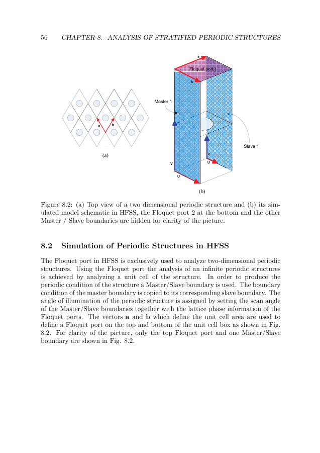
56 CHAPTER 8. ANALYSIS OF STRATIFIED PERIODIC STRUCTURES
Master 1
Slave 1
Floquet port 1
V
V
U
U
a
b
a b
(a)
(b)
Figure 8.2: (a) Top view of a two dimensional periodic structure and (b) its sim-ulated model schematic in HFSS, the Floquet port 2 at the bottom and the otherMaster / Slave boundaries are hidden for clarity of the picture.
8.2 Simulation of Periodic Structures in HFSS
The Floquet port in HFSS is exclusively used to analyze two-dimensional periodicstructures. Using the Floquet port the analysis of an infinite periodic structuresis achieved by analyzing a unit cell of the structure. In order to produce theperiodic condition of the structure a Master/Slave boundary is used. The boundarycondition of the master boundary is copied to its corresponding slave boundary. Theangle of illumination of the periodic structure is assigned by setting the scan angleof the Master/Slave boundaries together with the lattice phase information of theFloquet ports. The vectors a and b which define the unit cell area are used todefine a Floquet port on the top and bottom of the unit cell box as shown in Fig.8.2. For clarity of the picture, only the top Floquet port and one Master/Slaveboundary are shown in Fig. 8.2.

Chapter 9
Jaumann-Like Rasorber
A Jaumann absorber [71] is constructed by placing one or more resistive sheetsspaced a quarter wavelength apart in front of a metal plane in a stratified medium.It has been shown that Jaumann absorbers effectively reduce the back scatteringfrom planar [73] and curved structures [80] over a relatively wide frequency band.In this chapter the possibility of making a Jaumann absorber partially transparentat specific frequency and polarization is examined. This transparent window isbasically achieved by replacing the main blocking part of the Jaumann absorber,the back PEC, with an appropriate frequency selective circuit.
9.1 Design
A Gangbuster-Polarizer FSS
In this section, an FSS with proper filtering behavior for incoming electromagneticwaves is designed. The desired structure should ideally be totally reflective forone linearly polarized wave while having a band-stop behavior for the polarizationorthogonal to the first one. Furthermore, we are interested in a structure whichis rather robust in functioning, so that its behavior persists when it is bent overcurved surfaces. The band-stop behavior for one of the polarizations can be achievedby using a Gangbuster FSS [71] with dipoles parallel to the electric field of theincident wave. The Gangbuster structure can be superimposed with a periodicarray of infinitely long strips as shown in Fig. 9.1(a). These infinite strips providean almost perfect reflection for linearly polarized waves where the electric field isparallel to them. This cascading has no significant effect on the characteristicsof the Gangbuster. In order to support the resulting structure, the Gangbusterdipoles and infinite strips of the polarizer are embedded into a dielectric slab. Thecross section of the structure is shown in Fig. 9.1(b). Note that the Gangbusterdipoles and the polarized strips are not electrically connected to each other andare separated by a distance of t/3 inside the dielectric slab. The thickness and
57
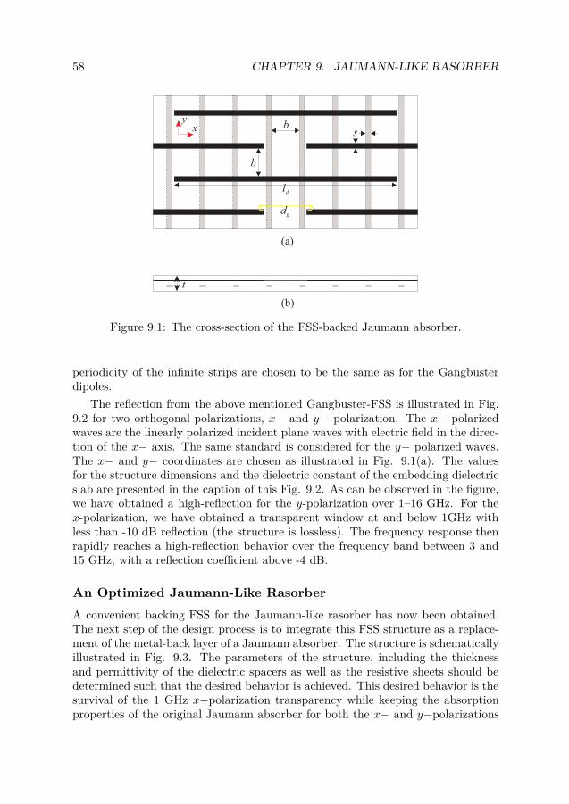
58 CHAPTER 9. JAUMANN-LIKE RASORBER
dg
b
b
ld
xy
s
t
(a)
(b)
Figure 9.1: The cross-section of the FSS-backed Jaumann absorber.
periodicity of the infinite strips are chosen to be the same as for the Gangbusterdipoles.
The reflection from the above mentioned Gangbuster-FSS is illustrated in Fig.9.2 for two orthogonal polarizations, x− and y− polarization. The x− polarizedwaves are the linearly polarized incident plane waves with electric field in the direc-tion of the x− axis. The same standard is considered for the y− polarized waves.The x− and y− coordinates are chosen as illustrated in Fig. 9.1(a). The valuesfor the structure dimensions and the dielectric constant of the embedding dielectricslab are presented in the caption of this Fig. 9.2. As can be observed in the figure,we have obtained a high-reflection for the y-polarization over 1–16 GHz. For thex-polarization, we have obtained a transparent window at and below 1GHz withless than -10 dB reflection (the structure is lossless). The frequency response thenrapidly reaches a high-reflection behavior over the frequency band between 3 and15 GHz, with a reflection coefficient above -4 dB.
An Optimized Jaumann-Like Rasorber
A convenient backing FSS for the Jaumann-like rasorber has now been obtained.The next step of the design process is to integrate this FSS structure as a replace-ment of the metal-back layer of a Jaumann absorber. The structure is schematicallyillustrated in Fig. 9.3. The parameters of the structure, including the thicknessand permittivity of the dielectric spacers as well as the resistive sheets should bedetermined such that the desired behavior is achieved. This desired behavior is thesurvival of the 1 GHz x−polarization transparency while keeping the absorptionproperties of the original Jaumann absorber for both the x− and y−polarizations
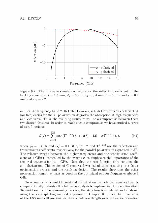
9.1. DESIGN 59
0 2 4 6 8 10 12 14 16
−10
−5
0
Freguency (GHz)
Refl
ecti
on
(dB
)
x−polarizedy−polarized
Figure 9.2: The full-wave simulation results for the reflection coefficient of thebacking structure. t = 1.5 mm, dg = 3 mm, ld = 8.4 mm, b = 3 mm and s = 0.4mm and εrs = 2.2
and for the frequency band 2–16 GHz. However, a high transmission coefficient atlow frequencies for the x−polarization degrades the absorption at high frequenciesand vice versa. Thus, the resulting structure will be a compromise between thesetwo desired features. In order to reach such a compromise we have studied a seriesof cost-functions:
G(f) =
160∑
l=10
max(Γx−pol(f0 + l∆f),−12) − wTx−pol(f0), (9.1)
where f0 = 1 GHz and ∆f = 0.1 GHz, Γx−pol and Tx−pol are the reflection andtransmission coefficients, respectively, for the parallel polarization expressed in dB.The relative weight between the higher frequencies and the transmission coeffi-cient at 1 GHz is controlled by the weight w to emphasize the importance of therequired transmission at 1 GHz. Note that the cost function only contains thex−polarization. This choice of G requires fewer calculations resulting in a fasteroptimization process and the resulting design. The results show that the otherpolarization remain at least as good as the optimized one for frequencies above 3GHz.
To accomplish this multidimensional optimization over a large frequency band iscomputationally intensive if a full wave analysis is implemented for each iteration.To avoid such a time consuming process, the structure is simulated and analyzedusing the wave splitting method explained in Chapter 8. Since the dimensionsof the FSS unit cell are smaller than a half wavelength over the entire operation
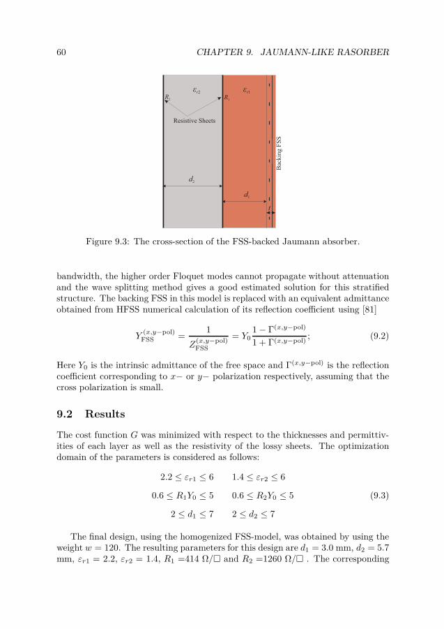
60 CHAPTER 9. JAUMANN-LIKE RASORBER
t
εr1
Resistive Sheets
εr2
Bac
king
FSS
d2
d1
R1R2
Figure 9.3: The cross-section of the FSS-backed Jaumann absorber.
bandwidth, the higher order Floquet modes cannot propagate without attenuationand the wave splitting method gives a good estimated solution for this stratifiedstructure. The backing FSS in this model is replaced with an equivalent admittanceobtained from HFSS numerical calculation of its reflection coefficient using [81]
Y(x,y−pol)
FSS =1
Z(x,y−pol)FSS
= Y01 − Γ(x,y−pol)
1 + Γ(x,y−pol); (9.2)
Here Y0 is the intrinsic admittance of the free space and Γ(x,y−pol) is the reflectioncoefficient corresponding to x− or y− polarization respectively, assuming that thecross polarization is small.
9.2 Results
The cost function G was minimized with respect to the thicknesses and permittiv-ities of each layer as well as the resistivity of the lossy sheets. The optimizationdomain of the parameters is considered as follows:
2.2 ≤ εr1 ≤ 6 1.4 ≤ εr2 ≤ 6
0.6 ≤ R1Y0 ≤ 5 0.6 ≤ R2Y0 ≤ 5 (9.3)
2 ≤ d1 ≤ 7 2 ≤ d2 ≤ 7
The final design, using the homogenized FSS-model, was obtained by using theweight w = 120. The resulting parameters for this design are d1 = 3.0 mm, d2 = 5.7mm, εr1 = 2.2, εr2 = 1.4, R1 =414 Ω/ and R2 =1260 Ω/ . The corresponding

9.2. RESULTS 61
reflection coefficients for the x− and y− polarizations are illustrated in Fig. 9.4. Thetransmission coefficient at the transparent window is ∼ −4dB. The full-wave resultshave a good agreement with the results obtained from the propagator model. Thestructure was investigated in detail in Paper IV. In paper IV, a sensitivity analysiswas also accomplished for the rasorber structure. The structure was also appliedto an elliptical layer of an aircraft wing front end. It is shown that the absorptioncharacteristics of the structure are robust when it is bent on a curved surface.
0 2 4 6 8 10 12 14 16−25
−20
−15
−10
−5
0
Freguency (GHz)
Refl
ecti
on
(dB
)
x−polarizedy−polarized
Figure 9.4: The reflection from the FSS-backed Jaumann absorber
One of the important factors in rasorber design is the transmission loss at thetransparent window. Using the conservation of power relation for a normally inci-dent plane wave of unit power, the loss of the structure is expressed as
P x−polloss = 1 − |Γx−pol|2 − |Tx−pol|2. (9.4)
The resistive loss of the Jaumann-like rasorber at its transparent window (1GHz) is 43%. This loss could be marginally lowered on the expense of losing partof the absorption bandwidth. However, this level of transmission loss is rather highfor a transparent window. In the next chapter, we introduce a different type ofrasorber that is based on a capacitive circuit absorber (CCA) [82]. Using a CCAin the rasorber design, the absorption characteristics are improved, transmissioncoefficient is increased and the loss at the transparent window is decreased. Fur-thermore, the CCA based design offers a thinner structure than the Jaumann basedcase.

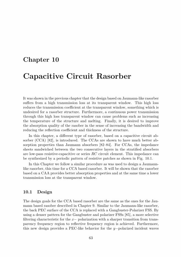
Chapter 10
Capacitive Circuit Rasorber
It was shown in the previous chapter that the design based on Jaumann-like rasorbersuffers from a high transmission loss at its transparent window. This high lossreduces the transmission coefficient at the transparent window, something which isundesired for a rasorber structure. Furthermore, a continuous power transmissionthrough this high loss transparent window can cause problems such as increasingthe temperature of the structure and melting. Finally, it is desired to improvethe absorption quality of the rasober in the sense of increasing the bandwidth andreducing the reflection coefficient and thickness of the structure.
In this chapter, a different type of rasorber, based on a capacitive circuit ab-sorber (CCA) [82], is introduced. The CCAs are shown to have much better ab-sorption properties than Jaumann absorbers [82–84]. For CCAs, the impedancesheets sandwiched between the two consecutive layers in the stratified absorbersare low-pass resistive-capacitive or series RC circuit element. This impedance canbe synthesized by a periodic pattern of resistive patches as shown in Fig. 10.1.
In this Chapter we follow a similar procedure as was used to design a Jaumann-like rasorber, this time for a CCA based rasorber. It will be shown that the rasorberbased on a CAA provides better absorption properties and at the same time a lowertransmission loss at the transparent window.
10.1 Design
The design goals for the CCA based rasorber are the same as the ones for the Jau-mann based rasober described in Chapter 9. Similar to the Jaumann-like rasorber,the back PEC surface of the CCA is replaced with a Gangbuster-Polarizer FSS. Byusing a denser pattern for the Gangbuster and polarizer FSSs [85], a more selectivefiltering characteristic for the x− polarization with a sharper transition from trans-parency frequency region to reflective frequency region is achieved. Furthermore,this new design provides a PEC-like behavior for the y−polarized incident waves
63
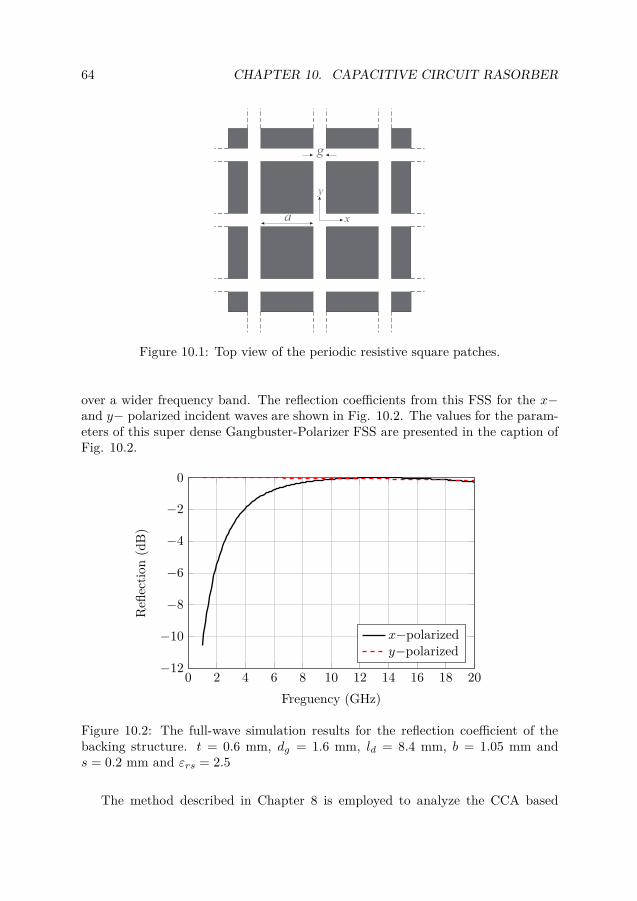
64 CHAPTER 10. CAPACITIVE CIRCUIT RASORBER
g
y
xa
Figure 10.1: Top view of the periodic resistive square patches.
over a wider frequency band. The reflection coefficients from this FSS for the x−and y− polarized incident waves are shown in Fig. 10.2. The values for the param-eters of this super dense Gangbuster-Polarizer FSS are presented in the caption ofFig. 10.2.
0 2 4 6 8 10 12 14 16 18 20−12
−10
−8
−6
−4
−2
0
Freguency (GHz)
Refl
ecti
on
(dB
)
x−polarizedy−polarized
Figure 10.2: The full-wave simulation results for the reflection coefficient of thebacking structure. t = 0.6 mm, dg = 1.6 mm, ld = 8.4 mm, b = 1.05 mm ands = 0.2 mm and εrs = 2.5
The method described in Chapter 8 is employed to analyze the CCA based

10.1. DESIGN 65
rasorber. The circuit model of a two layer CCA rasorber is shown in Fig. 10.3.The normalized equivalent series RC admittance that is sandwiched between layersis given by
Ysn0 =Ysn
Y0=
ω2Rn0C2n0
1 +R2n0ω
2C2n0
+ jωCn0
1 +R2n0ω
2C2n0
, (10.1)
where Rn0 = RnY0 and Cn0 = Cn/Y0, n is the number of boundary layers and Y0
is the intrinsic admittance of the free space. This admittance is implemented in(8.3) as the boundary condition between the consecutive layers. The structure isoptimized with a cost function similar to (9.1):
G =
200∑
l=10
max(Γx−pol(f0 + l∆f),−20) − wTx−pol(f0), (10.2)
where f0 = 1 GHz and ∆f = 0.1 GHz. Γx−pol and Tx−pol are respectively, thereflection and transmission coefficient for the x-polarized incidence in dB. The termw is a weight coefficient to make the single transmission coefficient large comparedto the summation terms of reflection coefficients. A good compromise betweentransmission at 1 GHz and absorption over the frequency band 2–20 GHz is obtainedby choosing w = 200.
R1R2
C1
d2 d1
Medium 1
C2
Free Space
ZFSS
Free Space Medium 2
Figure 10.3: Circuit model of a two layer FSS backed capacitive circuit absorber.
The cost function G is minimized with respect to the layer thicknesses,d1 andd2, and the admittance parameters R1, R2, C1 and C2, while the dielectric constantof the medium 1 and 2 layers are fixed at εr1 = 2.5 and εr1 = 1.4 respectively. Thefunction fmincon in Matlab 2010 is used for minimizing the cost function G overa range of parameter values. Several starting points are used in order to find thebest of the multiple local minima.

66 CHAPTER 10. CAPACITIVE CIRCUIT RASORBER
10.2 The Synthesis of the Series RC Admittances
The optimization process mentioned in the last section gives the values for capac-itances and resistances in the circuit model of the rasorber. This circuit modelshould be realized as a microwave structure.
The series RC circuits can be synthesized by an FSS pattern of square resistivepatches as shown in Fig. 10.1. An electrically dense grid of periodic conductivepatches has a capacitance of [86, 87]
C = ε0(εrc1 + εrc2)a+ g
πln(
1
sin( πg2(a+g) )
), (10.3)
provided that keff (a+g) ≪ 2π. Here, keff is the wave vector in the dielectric coverof the patches, εrc1 and εrc2 are the relative permittivity of the dielectric cover onthe top and bottom sides of the patches and a and g are shown in Fig. 10.1.
The corresponding lumped resistance approximation for a periodic pattern ofresistive square patches can also be obtained from [88,89]
R ≈ Rs(a+ g)2
a2, (10.4)
where Rs is the resistivity per square of the patch, and a and g are geometricparameters.
The above mentioned formulas can provide an estimate for the lumped R andC values of the periodic pattern of resistive patches. Nevertheless, for a CAAabsorber design, a more accurate RC synthesis is required. Such a synthesis can beaccomplished by a numerical curve fitting of the reflection coefficient from a seriesRC circuit and a periodic pattern of resistive patches embedded in a thin dielectriclayer. A series RC element in a transmission line with intrinsic impedance η0 isshown in Fig. 10.4. The voltage reflection coefficient from this RC impedance isgiven by [60]
Γ =ZL − η0
ZL + η0, (10.5)
where
ZL =
(
R+1
jωC
)
‖ η0. (10.6)
Substituting (10.6) into (10.5) and after some algebraic manipulation, the re-flection coefficient for the series RC impedance shunted in a transmission line gives
Γ =−jη0Cω
2(jRCω + 1) + jη0Cω. (10.7)

10.3. RESULTS AND DISCUSSION 67
R
C
η0
η0
Figure 10.4: A series RC element in a transmission line with intrinsic impedanceη0.
The best values for the patch resistivity, dimension and periodicity are achievedfrom an optimization process based on the reflection coefficient curve fitting. Inthis process, the absolute value of the reflection coefficient determined by full-waveanalysis of the coated periodic resistive patches are fitted to the corresponding curveachieved from (10.7) with the optimized R and C. Equations (10.4) and (10.3) areused to find an initial value for the patch resistivity, dimension and periodicity inthis optimization process.
10.3 Results and Discussion
The Module of Absorption Quality
In general, the desired property for radar absorbers is to provide the lowest possiblereflection within the widest operating frequency band, while having the least thick-ness. However, these requirements are contradictory to each other. In other words,reduction in the absorber’s total thickness results in shrinking the absorption band-width with a specific value of reflection coefficient. Using the frequency asymptoticbehavior of the reflection coefficient [90] and its analytical properties, Rozanov hasshown that the integral of the reflection coefficient from a metal back planar multi-layer slab, exposed to a normal incident plane wave, over the wavelength is boundedby a theoretical limit [91]
|∫ ∞
0
ln |R(λ)|dλ| ≤ 2π2∑
i
µs,idi, (10.8)
where di, µs,i are the thickness and the static permeability of ith layer of the strat-ified structure and λ is the wavelength in free apace.
If the module of the reflection coefficient of a radar absorber is less than ρ0
within the operating frequency band fmin − fmax, then
| ln(ρ0)|(λmax − λmin) < |∫ ∞
0
ln |R(λ)|dλ|, (10.9)

68 CHAPTER 10. CAPACITIVE CIRCUIT RASORBER
where, λmin and λmax are the wavelength corresponding to fmax and fmin respec-tively.
From (10.8) and (10.9) and for a non-magnetic absorber we have
| ln(ρ0)|λmax − λmin∑
i di< 2π2. (10.10)
The left hand side of the inequality (10.10) is the module of absorption. It isa measure of the radar absorber performance. The upper bound of this module ofabsorption, given by (10.10), gives the ultimate performance of an absorber. Thisbound can be used to evaluate an absorber design.
Numerical Results
Minimizing the cost function G gives the lumped element values for the circuitmodel of the rasorber. The resulting values of the optimized parameters are listedin Table 10.1. The circuit model then converted into an equivalent microwavestructure using the method described in Section 10.2. As shown in Equation (10.3),the equivalent capacitance depends on the dielectric constant of the coating layerson top and bottom of the resistive patches. In order to have the capacitanceunaffected by the permittivity of the rasorber layers, here the patches are coatedwith an ultra-thin dielectric layer with 0.2 mm thickness at each side. The dielectricconstant of the coating for each patch pattern is the same as the dielectric layerbelow, for example εi
rc1 = εirc2 = εi
rc = εri, where i denotes the medium number, 1or 2, in Fig. 10.3. The parameter values for the final realized microwave structure,equivalent to the RC circuit, with coated periodic resistive patches are shown inTable 10.2.
R1(Ω) R2(Ω) C1(pF) C2(pF) d1(mm) d2(mm)165.4 693.5 0.182 0.031 2.5 3.5
Table 10.1: The optimized parameters for the circuit model shown in Fig. 10.3
Rs1(Ω/) Rs2(Ω/) ε1rc ε2
rc
156 370 2.5 1.4
a1(mm) a2(mm) g1(mm) g2(mm)4.76 3.52 0.24 1.48
Table 10.2: The dimensions, resistivity of sheets and cover permittivities of theperiodic patches to realized the optimized equivalent lumped values.
The achieved three-dimensional model of the rasorber structure is implementedin Ansoft HFSS 12. A comparison between the homogeneous layer model approx-imation and the full-wave analysis of the realized structure, both illuminated by a

10.3. RESULTS AND DISCUSSION 69
normal incident wave in either y−polarization or x−polarization, is shown in Fig.10.5 and 10.6 respectively. It is shown that the reflection coefficient for the sim-plified model with stratified homogeneous layers (solid line) agrees well with thereflection coefficient of the full-wave analysis of the realized model (dashed line).The -20 dB absorption bandwidth for the x−polarized incidence and -19 dB ab-sorption bandwidth for the y−polarized incidence are, respectively, 8.4–19 GHz and6.6–19.1 GHz.
The values for x− polarized transmitted power at 1 GHz achieved by HFSSand circuit model are -1.9 dB and -1.6 dB, respectively. The designed structurecan therefore be classified as an e-class radome [92]. Furthermore, the transmissionloss of the structure defined by (9.4) is less than 10%. More details on the designprocess and results of this CCA rasober together with some perturbation studies, asensitivity analysis and power handling investigations can be found in Paper VI.
0 2 4 6 8 10 12 14 16 18 20−50
−40
−30
−20
−10
0
Freguency (GHz)
Refl
ecti
on
(dB
)
x−polarized
Full wave HFSSPropagator Model
Figure 10.5: Reflection coefficient of the optimized FSS backed CCA absorber forthe x−polarization

70 CHAPTER 10. CAPACITIVE CIRCUIT RASORBER
0 2 4 6 8 10 12 14 16 18 20−50
−40
−30
−20
−10
0
Freguency (GHz)
Refl
ecti
on
(dB
)
y−polarized
Full wave HFSSPropagator Model
Figure 10.6: Reflection coefficient of the optimized FSS backed CCA absorber forthe y−polarization

Chapter 11
Conclusion
The second part of this thesis was concerned with designing radar rasorbers. Thegoal of the project was to design a rasorber structure that is transparent at 1 GHzand lower for one linear polarization while it absorbs, as much as possible, theelectromagnetic waves for other frequencies or other polarization. Two rasorberdesigns, one based on Jaumann and the other based on CCA, were investigated.The wave splitting method was employed to model the rasorber structures. Usingthis simplified model a fast and efficient method was provided to analyze stratifiedstructures. The structures were optimized using this method and then synthesizedusing another optimization process. It was shown that The Jaumann-like rasorberdesign suffers from a high transmission loss at its transparent window. By utilizinga CCA, the transmission loss at the transparent window of the rasorber significantlydecreased. At the same time the design based on a CCA gave a larger absorptionover a wider bandwidth while having less thickness than the Jaumann-like rasorber.In other words, the rasorber based on a CCA design not only provided a highertransmission with lower transmission loss at its transparent window, but also hada much better module of absorption than the Jaumann-like rasorber.
The Jaumann-like rasorber was also applied to the curved surface of an aircraftwing front. It was shown that the characteristics of the Jaumann-like rasorber per-sist when it is used on elliptical surface of an aircraft wing front. As future research,the investigation of the characteristics of the CCA rasorber on curved structureswould be interesting. The collaboration of the rasorbers located at the near-fieldregion of an antenna is also an interesting future research suggestion. The effectsof the rasorber structures on antenna parameters, such as impedance, radiationpattern, and polarization properties, are interesting topics of investigation.
71
Bibliography
[1] A. Motevsselian, “On the scattering reduction of an aircraft wing profile en-closing an antenna,” Licentiate Thesis, Royal Institute of Technology (KTH),Stockholm, Sweden, June 2010.
[2] D. Hondros and P. Debye, “Elektromagnetische wellen an dielektrischendrähten,” Annalen der Physik, vol. 337, no. 8, pp. 465–476, 1910.
[3] G. E. Mueller and W. A. Tyrrell, “Polyrod antennas,” Bell System TechnicalJournal, vol. 337, no. 8, pp. 837–851, 1947.
[4] D. Halliday and D. Kiely, “Dielectric-rod aerials,” Electrical Engineers - PartIIIA: Radiocommunication, Journal of the Institution of, vol. 94, no. 14, pp.610 –618, 1947.
[5] R. B. Watson and C. W. Horton, “The radiation patterns of dielectric rods-experiment and theory,” Annalen der Physik, vol. 337, no. 8, pp. 661–670,Jan. 1948.
[6] C. W. Horton and J. C. M. McKinney, “An experimental investigation ofthe dielectric rod antenna of circular cross section excited in the dominantmode,” Journal of Applied Physics, vol. 22, no. 10, pp. 1246–1249, 1951.[Online]. Available: http://link.aip.org/link/?JAP/22/1246/1
[7] G. V. Trentini, “Polystyrene and lucite rod antennas,” Journal ofApplied Physics, vol. 24, no. 7, pp. 960–961, 1953. [Online]. Available:http://link.aip.org/link/?JAP/24/960/1
[8] R. D. Richtmyer, “Dielectric resonators,” Journal of Applied Physics, vol. 10,no. 6, pp. 391 –398, 1939.
[9] D. Kajfez and P. Guillon, Dielectric Resonators, 2’nd Edition. Nobel Pub-lishing Corporation, 1998.
[10] S. Cohn, “Microwave bandpass filters containing high-q dielectric resonators,”Microwave Theory and Techniques, IEEE Transactions on, vol. 16, no. 4, pp.218 – 227, 1968.
161

162 BIBLIOGRAPHY
[11] J. Van Bladel, “On the resonances of a dielectric resonator of very high per-mittivity,” Microwave Theory and Techniques, IEEE Transactions on, vol. 23,no. 2, pp. 199 – 208, 1975.
[12] S. A. Long, M. W. McAllister, and L. C. Shen, “The resonant cylindrical di-electric cavity antenna,” IEEE Trans. Antennas Propagat., vol. AP-31, no. 3,pp. 406–412, Mar. 1983.
[13] M. W. McAllister and S. A. Long, “Rectangular dielectric resonator antenna,”IEE Electron. Lett., vol. 19, pp. 218–219, Mar. 1983.
[14] ——, “Rectangular dielectric resonator antenna,” IEE Electron. Lett., vol. 20,pp. 657–659, Aug. 1984.
[15] K. Leung, “Simple result for conformal-strip excited hemispherical dielectricresonator antenna,” Electronics Letters, vol. 36, no. 11, pp. 933 – 935, May2000.
[16] K.-W. Leung, K.-M. Luk, K. Lai, and D. Lin, “Theory and experiment of anaperture-coupled hemispherical dielectric resonator antenna,” Antennas andPropagation, IEEE Transactions on, vol. 43, no. 11, pp. 1192 –1198, Nov.1995.
[17] A. A. Kishk, A. Ittipiboon, Y. M. M. Antar, and M. Cuhaci, “Slot excitationof the dielectric disk radiator,” IEEE Trans. Antennas Propagat., vol. AP-43,no. 2, pp. 198–201, Feb. 1995.
[18] R. Kumar Mongia and A. Ittipiboon, “Theoretical and experimental investi-gations on rectangular dielectric resonator antennas,” Antennas and Propa-gation, IEEE Transactions on, vol. 45, no. 9, pp. 1348 –1356, 1997.
[19] Y.-X. Guo, Y.-F. Ruan, and X.-Q. Shi, “Wide-band stacked double annular-ring dielectric resonator antenna at the end-fire mode operation,” Antennasand Propagation, IEEE Transactions on, vol. 53, no. 10, pp. 3394 – 3397,2005.
[20] K. Leung, W. Wong, K. Luk, and E. Yung, “Annular slot-coupled dielectricresonator antenna,” Electronics Letters, vol. 34, no. 13, pp. 1275 –1277, Jun.1998.
[21] S.-M. Deng, C.-L. Tsai, S.-F. Chang, and S.-S. Bor, “A cpw-fed suspended,low profile rectangular dielectric resonator antenna for wideband operation,”in Antennas and Propagation Society International Symposium, 2005 IEEE,vol. 4B, 2005, pp. 242 – 245 vol. 4B.
[22] R. K. Mongia, A. Ittipiboon, Y. M. M. Antar, P. Bhartia, and M. Cuhaci, “Ahalf-split cylindrical dielectric resonator antenna using slot-coupling,” IEEEMicrowave and Guided Wave Lett., vol. 3, no. 2, pp. 38–39, Feb. 1993.
BIBLIOGRAPHY 163
[23] A. Kishk, “Wide-band truncated tetrahedron dielectric resonator antennaexcited by a coaxial probe,” Antennas and Propagation, IEEE Transactionson, vol. 51, no. 10, pp. 2913 – 2917, 2003.
[24] A. A. Kishk, Y. Yin, and A. W. Glisson, “Conical dielectric resonator an-tenna for wideband application,” IEEE Trans. Antennas Propagat., vol. AP-50, no. 4, pp. 469–474, Apr. 2002.
[25] M. T. K. Tam and R. D. Murch, “Compact circular sector and anular sectordielectric resonator antenna,” IEEE Trans. Antennas Propagat., vol. AP-47,no. 5, pp. 837–342, May 1999.
[26] L. Zou and C. Fumeaux, “A cross-shaped dielectric resonator antenna formultifunction and polarization diversity applications,” Antennas and WirelessPropagation Letters, IEEE, vol. 10, pp. 742 –745, 2011.
[27] Y. Pan and K. W. Leung, “Wideband circularly polarized trapezoidal dielec-tric resonator antenna,” Antennas and Wireless Propagation Letters, IEEE,vol. 9, pp. 588 –591, 2010.
[28] L. Chu, D. Guha, and Y. Antar, “Conformal strip-fed shaped cylindricaldielectric resonator: Improved design of a wideband wireless antenna,” An-tennas and Wireless Propagation Letters, IEEE, vol. 8, pp. 482 –485, 2009.
[29] M. Oliver, Y. Antar, R. Mongia, and A. Ittipiboon, “Circularly polarisedrectangular dielectric resonator antenna,” Electronics Letters, vol. 31, no. 6,pp. 418 –419, Mar. 1995.
[30] R. Chair, A. Kishk, and K. Lee, “Wideband dual polarized dielectric res-onator antennas at x-band,” in Antennas and Propagation Society Interna-tional Symposium, 2005 IEEE, vol. 4B, 2005, pp. 214 – 217 vol. 4B.
[31] Y.-X. Guo and K.-M. Luk, “Dual-polarized dielectric resonator antennas,”Antennas and Propagation, IEEE Transactions on, vol. 51, no. 5, pp. 1120 –1124, May 2003.
[32] K. Leung, W. Wong, K. Luk, and E. Yung, “Circular-polarised dielectric res-onator antenna excited by dual conformal strips,” Electronics Letters, vol. 36,no. 6, pp. 484 –486, Mar. 2000.
[33] K. Leung, W. Wong, and H. Ng, “Circularly polarized slot-coupled dielectricresonator antenna with a parasitic patch,” Antennas and Wireless Propaga-tion Letters, IEEE, vol. 1, no. 1, pp. 57 –59, 2002.
[34] R. Mongia, A. Ittipiboon, M. Cuhaci, and D. Roscoe, “Circularly polariseddielectric resonator antenna,” Electronics Letters, vol. 30, no. 17, pp. 1361–1362, 1994.
164 BIBLIOGRAPHY
[35] K. W. Leung and S. K. Mok, “Circularly polarized dielectric resonator an-tenna excited by a perturbed annular slot with backing cavity,” Electron.Lett., vol. 34, no. 13, pp. 934–936, Jul. 2001.
[36] R. K. Mongia and P. Bhartia, “Dielectric resonator antennas-a review andgeneral design relations for resonant frequency and bandwidth,” Int. J. ofMicrowave and Millimeter-Wave Computer-Aided Engineering, vol. 4, no. 3,pp. 230–247, May 1994.
[37] A. Petosa, Dielectric resonator antenna handbook. Boston: Artech House,2007.
[38] R. F. Harrington, Time-Harmonic Electromagnetic Fields. New York: Wiley-Interscience, 2001.
[39] R. E. Collin, Field Theory of Guided Waves, 2’nd Edition. New York: Wiley-Interscience, 1991.
[40] C. A. Balanis, Antenna Theory: Analysis and Design, 3rd Edition. NewYork: Wiley, 1989.
[41] G. L. Yip and T. Auyeung, “Launching efficiency of the he11, surface-wavemode on a dielectric tube,” Microwave Theory and Techniques, IEEE Trans-actions on, vol. 22, no. 1, pp. 6 – 14, Jan. 1974.
[42] G. Yip, “Launching of the he11 surface-wave mode on a dielectric rod,” Elec-tronics Letters, vol. 6, no. 1, pp. 2 –3, Aug. 1970.
[43] G. L. Yip, “Launching efficiency of the he11 surface wave mode on a dielectricrod,” Microwave Theory and Techniques, IEEE Transactions on, vol. 18,no. 12, pp. 1033 – 1041, Dec. 1970.
[44] G. Yip and T. Au-Yeung, “Launching of the he/sub 11/ surface wave modeby an electric dipole imbedded in a dielectric rod,” in Microwave Symposium,G-MTT 1970 International, May 1970, pp. 245 –248.
[45] D. G. Kiely, Dielectric Aerials. New York: Wiley, 1952.
[46] C. De Young and S. Long, “Wideband cylindrical and rectangular dielec-tric resonator antennas,” Antennas and Wireless Propagation Letters, IEEE,vol. 5, no. 1, pp. 426 –429, Dec. 2006.
[47] K. W. Leung, H. Y. Lo, K. M. Luk, and E. K. N. Yung, “Two-dimensionalcylindrical dielectric resonator antenna array,” Electron. Lett., vol. 34, no. 13,pp. 1283–1285, Jun. 1998.
[48] Y. L. Hu, Z. H. Yang, J. Q. Li, and B. Li, “Backward-wave oscillation suppres-sion in high-power broadband helix traveling-wave tubes,” Electron Devices,IEEE Transactions on, vol. 58, no. 5, pp. 1562 –1569, May 2011.

BIBLIOGRAPHY 165
[49] P. Jain and B. Basu, “A theory of the attenuator-coated helical slow-wavestructure of a traveling-wave tube,” Electron Devices, IEEE Transactions on,vol. 35, no. 10, pp. 1750 –1757, 1988.
[50] D. A. Watkins, Topics in Electromagnetic Theory. New York: Wiley, 1958.
[51] H. Heffner, “Analysis of the backward-wave traveling-wave tube,” Proceedingsof the IRE, vol. 42, no. 6, pp. 930 –937, 1954.
[52] J. D. Kraus, Antennas, 2nd Edition. New York: McGraw-Hill, 1988.
[53] Y.-B. Jung and S.-Y. Eom, “Dual-band horn array design using a helicalexciter for mobile satellite communication terminals,” Antennas and Propa-gation, IEEE Transactions on, vol. 60, no. 3, pp. 1336 –1342, 2012.
[54] P. Cowles and E. Parker, “Helical feeds at millimetre wavelengths,” Electron-ics Letters, vol. 7, no. 18, pp. 513 –515, 1971.
[55] R. Johnson and R. Cotton, “A backfire helical feed,” Antennas and Propaga-tion, IEEE Transactions on, vol. 32, no. 10, pp. 1126 – 1128, 1984.
[56] S. Sensiper, “Electromagnetic wave propagation on helical conductorss,” MITRresearch Lab, Cambridge, Massachusetts, Tech. Rep. 194, May 1951.
[57] R. Mittra, “Wave propagation on helices,” Antennas and Propagation, IEEETransactions on, vol. 11, no. 5, pp. 585 – 586, 1963.
[58] C. A. Balanis, Antenna Theory: Analysis and Design, 3rd Edition. NewJersey: Wiley-Interscience, 2005.
[59] W. Hansen and J. Woodyard, “A new principle in directional antenna design,”Proceedings of the Institute of Radio Engineers, vol. 26, no. 3, pp. 333 – 345,1938.
[60] D. K. Cheng, Field and Wave Electromagnetics. Addison-Wesley Publishing.
[61] R. S. Elliot, Antenna Theory and Design, Revised Edition. New Jersey:Wiley-Interscience, 2003.
[62] J. Volakis, Antenna Engineering Handbook, 4th Edition. New York:McGraw-Hill, 2007.
[63] H. T. Hui, E. K. N. Yung, and K. W. Leung, “Numerical and experimentalstudies of a helical antenna loaded by a dielectric resonator,” Radio Sci.,vol. 32, no. 2, pp. 295 –304, Aug. 1997.
[64] C. Niow, K. Mouthaan, J. Coetzee, and H. Hui, “Design of a small sizedielectric loaded helical antenna for satellite communications,” in MicrowaveConference, 2009. APMC 2009. Asia Pacific, 2009, pp. 48 –51.
166 BIBLIOGRAPHY
[65] R. Vaughan and J. Andersen, “Polarization properties of the axial mode helixantenna,” Antennas and Propagation, IEEE Transactions on, vol. 33, no. 1,pp. 10 – 20, Jan. 1985.
[66] G. Almpanis, C. Fumeaux, and R. Vahldieck, “Offset cross-slot-coupled di-electric resonator antenna for circular polarization,” Microwave and WirelessComponents Letters, IEEE, vol. 16, no. 8, pp. 461 –463, Aug. 2006.
[67] L. Hady, A. Kishk, and D. Kajfez, “Dual-band compact dra with circular andmonopole-like linear polarizations as a concept for gps and wlan applications,”Antennas and Propagation, IEEE Transactions on, vol. 57, no. 9, pp. 2591–2598, 2009.
[68] A. Bondeson, Y. Yang, and P. Weinerfelt, “Optimization of radar cross sectionby a gradient method,” Magnetics, IEEE Transactions on, vol. 40, no. 2, pp.1260 – 1263, 2004.
[69] P. Ufimtsev, “Comments on diffraction principles and limitations of rcs re-duction techniques,” Proceedings of the IEEE, vol. 84, no. 12, pp. 1830 –1851,Dec. 1996.
[70] B. A. Munk, Metamaterials: Critique and Alternatives. pp. 61-70: NewYork: Wiley, 2009.
[71] ——, Frequency Selective Surfaces, Theory and Design. New York: Wiley,2000.
[72] J. Ramprecht and D. Sjoberg, “On the amount of magnetic material neces-sary in broadband magnetic absorbers,” in Antennas and Propagation SocietyInternational Symposium, 2008. AP-S 2008. IEEE, 2008, pp. 1 –4.
[73] E. F. Knott, J. F. Shaeffer, and M. T. Tuley, Radar Cross Section. Boston:Artech House, 1993.
[74] J. Ramprecht, M. Norgren, and D. Sjöberg, “Scattering from a thin magneticlayer with a periodic lateral magnetization: application to electromagneticabsorbers,” Progress In Electromagnetic Research, vol. 83, no. 3.
[75] P. Marin, D. Cortina, and A. Hernando, “Electromagnetic wave absorbingmaterial based on magnetic microwires,” Magnetics, IEEE Transactions on,vol. 44, no. 11, pp. 3934 –3937, Nov. 2008.
[76] J. A. Kong, Electromagnetic Theory. New York: Wiley, 1985.
[77] A. Karlsson and G. Kristensson, “Wave splitting in the time domain for aradially symmetric geometry,” Wave Motion, vol. 12, no. 3, pp. 197–211,1990. [Online]. Available: http://dx.doi.org/10.1016/0165-2125(90)90039-7

BIBLIOGRAPHY 167
[78] B. L. G. Jonsson and M. Norgren, “Asymptotic wave-splitting in anisotropiclinear acoustics,” Wave Motion, vol. 47, no. 5, pp. 318–326, 2010.
[79] A. K. Bhattacharyya, Phased Array Antennas. New York: Wiley-Interscience, 2005.
[80] A. Motevasselian and B. L. G. Jonsson, “Radar cross section reduction ofaircraft wing front end,” in Proc. IEEE Int. Conf. on Electromagnetics inAdvanced Applications, ICEAA, Turin, Italy, sep 2009, pp. 237–240.
[81] D. M. Pozar, Microwave Engineering. Addison Wesley, 2000.
[82] A. K. Zadeh and A. Karlsson, “Capacitive circuit method for fast and efficientdesign of wideband radar absorbers,” IEEE Trans. Antennas Propagat., vol.AP-57, no. 8, pp. 2307–2314, Aug. 2009.
[83] A. Kazemzadeh and A. Karlsson, “On the absorption mechanism of ultrathin absorbers,” IEEE Trans. Antennas Propagat., vol. AP-58, no. 10, pp.3310–3315, Oct. 2010.
[84] A. Kazemzadeh, “Thin wideband absorber with optimal thickness,” in Elec-tromagnetic Theory (EMTS), 2010 URSI International Symposium on, Aug.2010, pp. 676 –679.
[85] S. W. Schneider and B. A. Munk, “The scattering properties of super densearrays of dipoles,” IEEE Trans. Antennas Propagat., vol. AP-42, no. 2, pp.463–472, Apr. 1994.
[86] O. Luukkonen, F. Costa, C. R. Simovski, A. Monorchio, and S. A. Tretyakov,“A thin electromagnetic absorber for wide incidence angles and both polariza-tions,” IEEE Trans. Antennas Propagat., vol. AP-57, no. 10, pp. 3119–3125,Oct. 2009.
[87] S. Tretyakov, Analytical Modeling in Applied Electromagnetics. Boston:Artech House, 2003.
[88] K. W. Whites and R. Mittra, “An equivalent boundary-condition model forlossy planar periodic structures at low frequencies,” IEEE Trans. AntennasPropagat., vol. AP-44, no. 12, pp. 1617–1628, Dec. 1996.
[89] F. Costa, A. Monorchio, and G. Manara, “Analysis and design of ultra thinelectromagnetic absorbers comprising resistively loaded high impedance sur-faces,” IEEE Trans. Antennas Propagat., vol. AP-58, no. 5, pp. 1551–1558,May 2010.
[90] L. M. Brekhovskikh, Waves in layered media. New York: Academic Press,1980.
168 BIBLIOGRAPHY
[91] K. N. Rozanov, “Ultimate thickness to bandwidth ratio of radar absorbers,”IEEE Trans. Antennas Propagat., vol. AP-48, no. 8, pp. 1230–1234, Aug.2000.
[92] D. J. Kozakoff, Analysis of Radome-enclosed Antennas 2’nd Edition. Boston:Artech House, 2010.
[93] E. Lim, K. Leung, and X. Fang, “The compact circularly-polarized hollowrectangular dielectric resonator antenna with an underlaid quadrature cou-pler,” Antennas and Propagation, IEEE Transactions on, vol. 59, no. 1, pp.288 –293, 2011.
[94] L. Hady, A. Kishk, and D. Kajfez, “Dual-band compact dra with circular andmonopole-like linear polarizations as a concept for gps and wlan applications,”Antennas and Propagation, IEEE Transactions on, vol. 57, no. 9, pp. 2591–2598, 2009.
[95] A. A. Kishk, “An elliptic dielectric resonator antenna designed forcircular polarization with single feed,” Microwave and Optical Technol-ogy Letters, vol. 37, no. 6, pp. 454–456, 2003. [Online]. Available:http://dx.doi.org/10.1002/mop.10948
[96] B. Li, C.-X. Hao, and X.-Q. Sheng, “A dual-mode quadrature-fed widebandcircularly polarized dielectric resonator antenna,” Antennas and WirelessPropagation Letters, IEEE, vol. 8, pp. 1036 –1038, 2009.
[97] K. Leung, “Circularly polarized dielectric resonator antenna excited by ashorted annular slot with a backing cavity,” Antennas and Propagation, IEEETransactions on, vol. 52, no. 10, pp. 2765 – 2770, 2004.
[98] K. W. Leung and H. K. Ng, “Theory and experiment of circularly polarizeddielectric resonator antenna with a parasitic patch,” Antennas and Propaga-tion, IEEE Transactions on, vol. 51, no. 3, pp. 405 – 412, 2003.
[99] M. Simeoni, R. Cicchetti, A. Yarovoy, and D. Caratelli, “Plastic-based super-shaped dielectric resonator antennas for wide-band applications,” Antennasand Propagation, IEEE Transactions on, vol. 59, no. 12, pp. 4820 –4825, Dec.2011.
[100] K.-W. Khoo, Y.-X. Guo, and L. C. Ong, “Wideband circularly polarizeddielectric resonator antenna,” Antennas and Propagation, IEEE Transactionson, vol. 55, no. 7, pp. 1929 –1932, Jul. 2007.
[101] S. Malekabadi, M. Neshati, J. Rashed, and A. Attari, “Circular polarizedcylindrical dielectric resonator antenna using a single probe feed,” in Mi-crowave and Millimeter Wave Technology, 2008. ICMMT 2008. InternationalConference on, vol. 3, Apr. 2008, pp. 1098 –1101.
BIBLIOGRAPHY 169
[102] B. Li, K. So, and K. Leung, “A circularly polarized dielectric resonator an-tenna excited by an asymmetrical u-slot with a backing cavity,” Antennasand Wireless Propagation Letters, IEEE, vol. 2, no. 1, pp. 133 –135, 2003.
[103] C.-Y. Huang, J.-Y. Wu, and K.-L. Wong, “Cross-slot-coupled microstrip an-tenna and dielectric resonator antenna for circular polarization,” Antennasand Propagation, IEEE Transactions on, vol. 47, no. 4, pp. 605 –609, 1999.
[104] C.-Y. Huang and C.-W. Ling, “Frequency-adjustable circularly polarised di-electric resonator antenna with slotted ground plane,” Electronics Letters,vol. 39, no. 14, pp. 1030 – 1031, 2003.
[105] H. Nakano, S. Kirita, N. Mizobe, and J. Yamauchi, “External-excitation curlantenna,” Antennas and Propagation, IEEE Transactions on, vol. 59, no. 11,pp. 3969 –3977, 2011.
[106] T. A. Latef and S. K. Khamas, “Measurements and analysis of a helicalantenna printed on a layered dielectric hemisphere,” IEEE Trans. AntennasPropagat., vol. 59, no. 12, pp. 4831 –4835, 2011.
[107] T.-S. Chu and N. Kilcoyne, “The excitation of a dielectric-rod antenna bya helix,” Antennas and Propagation, IRE Transactions on, vol. 9, no. 4, pp.416 –417, 1961.
[108] A. Motevasselian, A. Ellgardt, and B. L. G. Jonsson, “A circularly polar-ized cylindrical dielectric resonator antenna using a helical exciter,” To beSubmitted to IEEE Trans. Antennas Propagat.
[109] M. Heneishi and H. Takazawa, “Broadband circularly polarised palannar ar-ray composed of a pair of dielectric resonator antennas,” IEE Electron. Lett.,vol. 21, pp. 437–438, May 1985.
[110] A. Kishk, B. Ahn, and D. Kajfez, “Broadband stacked dielectric resonatorantennas,” Electronics Letters, vol. 25, no. 18, pp. 1232 –1233, aug. 1989.
[111] P. Hannan, “The element-gain paradox for a phased-array antenna,” IEEETrans. Antennas Propagat., vol. AP-12, no. 4, pp. 423–433, Jul. 1964.
[112] R. J. Dorris, R. T. Long, S. A. Long, M. A. Khayat, and J. T. William, “Mu-tual coupling between cylindrical probe-fed dielectric resonator antennas,”IEEE Antennas Wireless Propagat. Lett, vol. 1, pp. 8–9, 2002.
[113] Y. X. Guo, K. M. Luk, and K. W. Leung, “Mutual coupling betweenmillimeter-wave dielectric resonator antennas,” IEEE Trans. Microw. The-ory Tech., vol. 47, no. 11, pp. 2164–2166, Nov. 1999.
170 BIBLIOGRAPHY
[114] R. Chair, A. A. Kishk, and K.-F. Lee, “Comparative study on the mutualcoupling between different sized cylindrical dielectric resonators antennas andcircular microstrip patch antennas,” IEEE Trans. Antennas Propagat., vol.AP-53, no. 3, pp. 1011–1019, Mar. 2005.
[115] A. Ellgardt and M. Norgren, “Edge element evaluation of tapered-slot ele-ments in phased arrays,” in Antennas and Propagation (EuCAP), 2010 Pro-ceedings of the Fourth European Conference on, 2010, pp. 1 –5.
[116] ——, “A study of edge effects in triangular grid tapered-slot arrays usingcoupling coefficients,” Radio Science, vol. 45, Apr. 2010.
[117] G. P. Junker, A. A. Kishk, and A. W. Glisson, “Input impedance of dielec-tric resonator antennas excited by a coaxial probe,” IEEE Trans. AntennasPropagat., vol. AP-42, no. 7, pp. 960–966, Jul. 1994.
[118] C. Craeye and M. Arts, “On the receiving cross section of an antenna ininfinite linear and planar arrays,” Radio Science, vol. 39, no. 2, Apr. 2004.
[119] E. Knott and K. Langseth, “Performance degradation of jaumann absorbersdue to curvature,” IEEE Trans. Antennas Propagat., vol. AP-28, no. 1, pp.137–139, Jan. 1980.
[120] B. Chambers and A. Tennant, “Optimum design of cylindrical Jaumann ab-sorbers,” in Ninth International Conference on Antennas and propagations,1995, pp. 450–454.
[121] W. W. Salisbury, “Absorbent body for electromagnetic waves,” United StatesPatent 2,599,944, June 1954.
[122] W. H. Emerson, “Electromagnetic wave absorbers and anechoic chambersthrough the years,” IEEE Trans. Antennas Propagat., vol. AP-21, pp. 484–490, Jul. 1973.
[123] L. J. du Toit, “The design of Jaumann absorbers,” IEEE Antennas Propagat.Mag, vol. 36, pp. 17–25, Dec. 1994.
[124] F. Sakran, Y. Neve-Oz, M. G. A. Ron, D. Davidov, and A. Frenkel, “Absorb-ing frequency-selective-surface for the mm-wave range,” IEEE Trans. Anten-nas Propagat., vol. AP-56, no. 8, pp. 2649–2655, Aug. 2008.
[125] “Techniques for analyzing frequency selective surfaces-a review,” Proceedingsof the IEEE, vol. 76, no. 12, pp. 1593 –1615, Dec. 1988.
[126] E. Martini, F. Caminita, M. Nannetti, and S. Maci, “Fast analysis of fssradome for antenna rcs reduction,” in Proc. IEEE Int. Symp. on Antennasand Propagation Society, July 2006, pp. 1801–1804.

BIBLIOGRAPHY 171
[127] H. Chen, X. Hou, and L. Deng, “Design of frequency-selective surfaces radomefor a planar slotted waveguide antenna,” IEEE Antennas and Wireless Prop-agat. Lett, vol. 8, pp. 1231–1233, 1980.
[128] C. Sabah1 and S. Uçkun, “Electromagnetic wave propagation throughfrequency-dispersive and lossy double-negative slab,” Opto-Electronics Re-view, vol. 15, no. 3, pp. 133–143, Sep. 2007.
[129] A. Charles, M. S. Towers, and A. McCowen, “Sensitivity analysis of jaumannabsorbers,” in Proc. IEE Microwaves, Antennas and Propagation, August1999, pp. 257–262.
[130] B. Munk, P. Munk, and J. Prior, “On designing Jaumann and circuit ana-log absorbers (CA Absorbers) for oblique angle of incidence,” IEEE Trans.Antennas Propagat., vol. AP-55, no. 1, pp. 186–193, Jan. 2007.
[131] E. F. Knott and C. D. Lunden, “The two-sheet capacitive Jaumann absorber,”IEEE Trans. Antennas Propagat., vol. AP-43, no. 11, pp. 1339–1343, Nov.1995.
[132] A. Itou, O. Hashimoto, H. Yokokawa, and K. Sumi, “A fundamental studyof thin λ/4 wave absorber using FSS technology,” Electron. Commun. Jpn.,vol. 87, no. 11, pp. 77–86, 2004.
[133] A. Motevasselian and B. L. G. Jonsson, “A partially transparent Jaumannabsorber applied to an aircraft wing profile,” in Proc. IEEE Int. Symp. An-tennas and Propagation Society, July 2010.
[134] ——, “Partially transparent jaumann like absorber applied to a curvedstructure,” International Journal of Antennas and Propagation, vol. 2011,2011. [Online]. Available: http://dx.doi.org/10.1155/2011/708987
[135] F. B. Gross and E. J. Kuster, “An optimized polarization sensitive Salisburyscreen,” IEEE Trans. Antennas Propagat., vol. AP-35, no. 12, pp. 1492–1495,Dec. 1987.
[136] F. Costa and A. Monorchio, “Absorptive frequency selective radome,” in Gen-eral Assembly and Scientific Symposium of the International Union of RadioScience (URSI), Proceedings of, Aug. 2011.
[137] M. Salehi and N. Behdad, “A second-order dual x-/ka-band frequency se-lective surface,” IEEE Microw. Wireless Compon. Lett., vol. 18, no. 12, pp.785–787, Dec. 2008.
[138] M. A. Al-Joumayly and N. Behdad, “A generalized method for synthesizinglow-profile, band-pass frequency selective surfaces with non-resonant consti-tuting elements,” IEEE Trans. Antennas Propagat., vol. AP-58, no. 12, pp.4033–4041, Dec. 2010.

172 BIBLIOGRAPHY
[139] R. E. Collin, Foundations for Microwave Engineering 2’nd Edition. pp.42-43: New York: McGraw-Hill, 1992.
[140] B. A. Munk, R. G. Kouyoumjian, and L. P. Jr., “Reflection properties ofperiodic surfaces of loaded dipoles,” IEEE Trans. Antennas Propagat., vol.AP-19, pp. 612–617, Sep. 1971.
[141] A. Kazemzadeh, “Nonmagnetic ultrawideband absorber with optimal thick-ness,” IEEE Trans. Antennas Propagat., vol. AP-59, no. 1, pp. 135–140, Jan.2011.