Electroless Deposition of Confined Copper Layers Based on ... · Electroless deposition is usually...
7
JLMN-Journal of Laser Micro/Nanoengineering Vol. 12, No. 2, 2017 169 Electroless Deposition of Confined Copper Layers Based on Selective Activation by Pulsed Laser Irradiation Rui Zhou * , Tingting Huang, Lijuan Chen, Sijie Chen, Shengdong Lin and Yong Zhuo School of Aerospace Engineering, Xiamen University, 422 Siming South Road, Siming District, Xiamen, Fujian Province, China 361005 *E-mail: [email protected] Copper circuit was successfully fabricated on non-conductive modified polycarbonate (PC) lightweight plastic substrate by pulsed laser ablation. The modified PC plastic embedded with cop- per nanoparticles provides a possible route for electroless copper deposition. Copper layer can be selectively confined in the area of pulsed laser activation on the PC substrate. Laser ablation can remove the polymeric substrate material with controlled processing parameters and make embedded copper seeds exposed as self-catalytic centers. In this work, the effects of laser power and scanning speed on the electrical performance of deposited copper layer are investigated. Energy Dispersive X-ray (EDX) is employed to analyze the surface chemistry of activated areas. The dynamic process and deposition mechanism of copper layer on PC surface are studied. The resistivity of the copper layer is strongly dependent on laser power and scanning speed. An optimized resistivity of 15 μΩ·cm is achieved. Keywords: pulsed laser ablation, selective activation, modified polycarbonate, copper deposition, resistivity 1. Introduction Lightweight technology is now a raising focus which has great potentials in a wide range of applications in port- able microelectronics, wearable device, and flexible sensor 1-4 . Therefore flexible substrate with various electronic functions is highly demanded. Several researchers have conducted the fabrication of electronic devices on different substrates, such as silver resonator on ceramic 5 , copper circuit on nylon PA2200 6 , and copper nanostructure on sillicon 7 . In order to fabricate metal film with flexible pat- tern design and great performance, various methods of metallization are developed. M. Farhan Shafique et al. used silver paste to coat the substrate first and then etch the un- wanted part with laser ablation afterwards 5 . Matteo Calaon et al. fabricated a Al foil mask and deposited copper on the uncovered areas with physical vapour deposition (PVD) method 8 . Shih-Chun Huang et al. deposited copper film on polymer substrates with the aid of EDA ink by electroless deposition 9 . Although these methods could finally realize the film metallization, it has involved quite complicated processing with the shortage of sufficient flexibility. Electroless deposition is usually known as self-catalytic reduction of dissolved metal ions by reducing agent at the solid-liquid interface. Since 1950s, the electroless deposi- tion techniques were rapidly developed for the growing market of printed circuits. Furthermore, it has been widely applicable for integrated circuits, decorative articles and semiconductors 10 . Commonly, electroless copper deposi- tion on insulators, including plastics, glass and ceramics 11, 12 , is considered as a chemically complex process mainly consisted of four steps: etching, neutralization, catalysis and electroless plating 13 . Accordingly, it is desirable to explore a flexible and straightforward way to realize the fabrication of various patterns on non-conductive substrate. Laser activation as an alternative step, instead of etching, neutralization and ca- talysis, mainly reduces the processing complexity 14 . Meanwhile, laser processing as an environmental friendly and easy operation tool can achieve flexibly designed pat- terns 15, 16 . A lot of effort has been carried out mainly in three aspects. Firstly, the selection of electroless deposition solution could be extended. Milan Paunovic and Russ Arndt concluded that guanine and adenine can accelerate electroless copper deposition 17 . Fumihiro Inoue et al. stud- ied copper bath stability by UV-Visible spectrum and PH measurement 18 . Secondly, the system setup could be intel- ligently optimized for laser processing equipment. Lothar Bauer developed an offline programming module for laser systems 19 . Fanhui Meng and Hongzhi Wang also developed a CAD/CAM software for laser micromachining 20 . Finally, substrates with blended catalytic seeds could be intendedly modified. The patent invented by LPKF Company demon- strated a modified plastic substrate by mixing organometal- lic complex 21 . However, few studies have been performed to optimize the laser processing parameters and understand the mechanism, which could have significant impact on the quality of deposited metal layer. In this paper, we present a highly accurate and flexible method to fabricate confined copper layer on PC plastic by pulsed laser ablation. It involves the commercially im- proved grade of electroless deposition solution and modi- fied PC plastic substrate. Etching, neutralization and catal- ysis (including stannum sensitization and palladium activa- tion) process in conventional techniques have been auto- matically avoided. During the electroless deposition pro- cess, pulsed laser ablation is used to activate the surface of the PC plastic with specifically designed patterns. The modified PC plastic substrate contains active copper seeds, Technical Communication DOI: 10.2961/jlmn.2017.02.0021
Transcript of Electroless Deposition of Confined Copper Layers Based on ... · Electroless deposition is usually...
JLMN-Journal of Laser Micro/Nanoengineering Vol. 12, No. 2, 2017
169
Electroless Deposition of Confined Copper Layers Based on Selective Activation by Pulsed Laser Irradiation
Rui Zhou*, Tingting Huang, Lijuan Chen, Sijie Chen, Shengdong Lin and Yong Zhuo
School of Aerospace Engineering, Xiamen University, 422 Siming South Road, Siming District, Xiamen, Fujian Province, China 361005
*E-mail: [email protected]
Copper circuit was successfully fabricated on non-conductive modified polycarbonate (PC) lightweight plastic substrate by pulsed laser ablation. The modified PC plastic embedded with cop-per nanoparticles provides a possible route for electroless copper deposition. Copper layer can be selectively confined in the area of pulsed laser activation on the PC substrate. Laser ablation can remove the polymeric substrate material with controlled processing parameters and make embedded copper seeds exposed as self-catalytic centers. In this work, the effects of laser power and scanning speed on the electrical performance of deposited copper layer are investigated. Energy Dispersive X-ray (EDX) is employed to analyze the surface chemistry of activated areas. The dynamic process and deposition mechanism of copper layer on PC surface are studied. The resistivity of the copper layer is strongly dependent on laser power and scanning speed. An optimized resistivity of 15 μΩ·cm is achieved.
Keywords: pulsed laser ablation, selective activation, modified polycarbonate, copper deposition, resistivity
1. Introduction Lightweight technology is now a raising focus which
has great potentials in a wide range of applications in port-able microelectronics, wearable device, and flexible sensor 1-4. Therefore flexible substrate with various electronic functions is highly demanded. Several researchers have conducted the fabrication of electronic devices on different substrates, such as silver resonator on ceramic5, copper circuit on nylon PA22006, and copper nanostructure on sillicon7. In order to fabricate metal film with flexible pat-tern design and great performance, various methods of metallization are developed. M. Farhan Shafique et al. used silver paste to coat the substrate first and then etch the un-wanted part with laser ablation afterwards5. Matteo Calaon et al. fabricated a Al foil mask and deposited copper on the uncovered areas with physical vapour deposition (PVD) method8. Shih-Chun Huang et al. deposited copper film on polymer substrates with the aid of EDA ink by electroless deposition9. Although these methods could finally realize the film metallization, it has involved quite complicated processing with the shortage of sufficient flexibility.
Electroless deposition is usually known as self-catalytic reduction of dissolved metal ions by reducing agent at the solid-liquid interface. Since 1950s, the electroless deposi-tion techniques were rapidly developed for the growing market of printed circuits. Furthermore, it has been widely applicable for integrated circuits, decorative articles and semiconductors10. Commonly, electroless copper deposi-tion on insulators, including plastics, glass and ceramics11,
12, is considered as a chemically complex process mainly consisted of four steps: etching, neutralization, catalysis and electroless plating13.
Accordingly, it is desirable to explore a flexible and straightforward way to realize the fabrication of various
patterns on non-conductive substrate. Laser activation as an alternative step, instead of etching, neutralization and ca-talysis, mainly reduces the processing complexity14. Meanwhile, laser processing as an environmental friendly and easy operation tool can achieve flexibly designed pat-terns15, 16. A lot of effort has been carried out mainly in three aspects. Firstly, the selection of electroless deposition solution could be extended. Milan Paunovic and Russ Arndt concluded that guanine and adenine can accelerate electroless copper deposition17. Fumihiro Inoue et al. stud-ied copper bath stability by UV-Visible spectrum and PH measurement 18. Secondly, the system setup could be intel-ligently optimized for laser processing equipment. Lothar Bauer developed an offline programming module for laser systems19. Fanhui Meng and Hongzhi Wang also developed a CAD/CAM software for laser micromachining20. Finally, substrates with blended catalytic seeds could be intendedly modified. The patent invented by LPKF Company demon-strated a modified plastic substrate by mixing organometal-lic complex21. However, few studies have been performed to optimize the laser processing parameters and understand the mechanism, which could have significant impact on the quality of deposited metal layer.
In this paper, we present a highly accurate and flexible method to fabricate confined copper layer on PC plastic by pulsed laser ablation. It involves the commercially im-proved grade of electroless deposition solution and modi-fied PC plastic substrate. Etching, neutralization and catal-ysis (including stannum sensitization and palladium activa-tion) process in conventional techniques have been auto-matically avoided. During the electroless deposition pro-cess, pulsed laser ablation is used to activate the surface of the PC plastic with specifically designed patterns. The modified PC plastic substrate contains active copper seeds,
Technical Communication
DOI: 10.2961/jlmn.2017.02.0021

JLMN-Journal of Laser Micro/Nanoengineering Vol. 12, No. 2, 2017
170
which serve as the self-catalytic centers. The surface mor-phologies of laser machined plastic and the copper layer after metallization are observed by scanning electron mi-croscopy (SEM) to understand the process of copper depo-sition. This work could benefit systematic understanding of the tunable laser parameters effects on the film quality and electrical performance, thus further guide us to deposit copper layer under other non-conductive substrates by la-ser. 2. Experimental Materials
The non-conductive PC plastic (HALCYON 5H003, ShenZhen) is used as substrate materials. With the premise of necessary mechanical and thermal properties, such as tenacity, hardness and melting point, Cu powder is mixed with the polycarbonate as much as possible. The PC sub-strate is formed by injection of the modified PC particles with a thickness 3 mm. Electroless copper deposition is supported by the dissolved solution (STELLA SSC_ECU_18, Singapore). The chemicals named SCC_ECU_18_A mainly contain copper sulfate as copper ion provider and formaldehyde as the reducing agent. Solu-tion SCC_ECU_18_B mainly contains sodium hydroxide which is used to control the PH of chemical solution.
Selective activation by pulsed laser ablation
Fig.1 shows the process of laser selective activation of electroless copper deposition. The sample is prepared with the fixed size of 25mm x 40mm x 3mm. First of all, ultra-sonicator is used to clean the PC plastic substrate with al-cohol. The impurities generated from oil, ash or fingerprint could have complex and unexpected interaction with laser. Then it is of great importance to guarantee the cleanness of the plastic surface. Subsequently, the PC plastic surface is irradiated by pulsed fiber laser with 16 groups of combined parameters. The wavelength of the laser is 1064 nm. The pulse duration is 100 ns and the repetition is 20 kHz. The spot size is ~50 μm. The laser power is changed from 0.9 W to 1.4 W and scanning speed is changed from 450 mm/s to 600 mm/s in order to investigate their influence on cop-per deposition. An exhauster is used to pump air with va-porized plume. After laser irradiation, the substrate was treated again with alcohol to remove the residue on the PC plastic surface.
Fig.1 Schematic process of laser selective activation of electroless
copper deposition.
Copper layer deposition Fig.1 also shows the schematic process of copper met-
allization. SCC_ECU_18_A and SCC_ECU_18_B are re-spectively mixed with the volume ratio of 3:2 and then mechanically agitated for 5 minutes. The mixed solution is evenly heated in a water bath. The temperature is raised to ~50 ℃ by a fixed heating stage in order to speed up chemi-cal reactions. It was observed that scattered brownish spots are on the surface at the very beginning and then the color of the surface gradually becomes darker. During this pro-cess, microbubbles could be observed. The thickness of the copper layer is related to the metallization time and usually the film can become electrically conductive in ~2 hours. Afterwards, the substrate is immersed with an antioxidant to inhibit the oxidation.
Electrical measurement
The resistance of each copper film is measured using 2-wire Ohms measurement. The contact resistance is com-pensated. Each set of data is measured three times and then averaged to minimize the experimental errors.
Material characterization
Surface morphology is investigated by scanning elec-tron microscope (Hitachi Su-70, Japan). Resistivity is measured by LCR meter (HIOKI IM3532, Japan). 3. Results and discussion Morphology and chemical compositions
Fig.2 SEM images and EDX results of laser processed PC plastic
substrate.

JLMN-Journal of Laser Micro/Nanoengineering Vol. 12, No. 2, 2017
171
The surface of PC plastic is fully composed of irregu-larly shaped holes and residues as shown in Fig.2(a). While PC plastic is irradiated by pulsed laser, the generated heat dissipates into the substrate by absorption of the pulsed laser and then the bulk temperature is raised up. The heat-affected zone can change the surface morphology by re-casting and formation of burrs. As the laser intensity reach-es a certain level, the number of species within the plume exponentially increases by interaction with the laser beam which ionizes the molecules, leading to the formation of plasma plume. In the laser ablation, compressive forces can be created by the vapor and plasma plume at the laser focused point, leading to the expulsion of the molten pool of materials. The sputtered nanoparticles are solidified in air and then pushed away by the shock waves accompanied by plasma plume, which are finally absorbed by the ex-hauster. Attributed to the Gaussian distribution of the laser beam at the focus point, the vicinal area of laser ablation can absorb less energy with lower temperature, contrib-
uting to the generation of smaller holes around central holes. Meanwhile, the chemical compositions of the PC plastic surface have been changed. Fig.2(b) shows the atomic percentages of various elements on the PC plastic surface before and after laser irradiation. Before pulsed laser ablation, the elements of C and O play the major roles and only 0.17% Cu exists. Since copper powder is blended inside the PC plastic, 20.03% atomic percentage of Cu was detected in the laser irradiated area. Other elements, such as Al, Si, Ti, Zn, P, are mixed up to enhance the thermody-namic properties of the PC plastic. The existence of Cu seeds provides the feasibility of electroless copper deposi-tion. Evolution of copper deposition To investigate the mechanism of copper layer deposition on laser irradiated PC plastic surface, SEM is employed to observe the dynamic growth behaviors of deposited copper layer in different phases.
Fig.3 SEM images of copper deposition process in different periods: (a) copper emerging from laser created cracks on PC plastic surface;
(b) copper particles aggregate to copper islands; (c) bonding of copper islands; and (d) formation of copper film.
Figs.3(a-d) describe the dynamic process of the copper deposition. As shown in Fig.3(a), the width of the hole is ~ 3 µm and the length is ~10 µm., The surface absorbs the short-duration laser pulse with concomitant electronic transitions from the ground singlet state to the first excited singlet state and broke the bond within the long-chain
polymers22. The generated flow consists of gases (CO2, CO) and carbonaceous particles are ejected into air 22, 23. The dynamic process removes the surface materials and creates holes. The shape and size of the holes are deter-mined by material physical and chemical properties, such as thermal conductivity coefficient, specific heat capacity,
JLMN-Journal of Laser Micro/Nanoengineering Vol. 12, No. 2, 2017
172
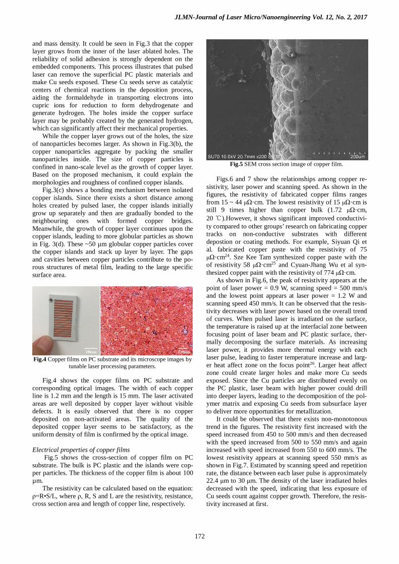
and mass density. It could be seen in Fig.3 that the copper layer grows from the inner of the laser ablated holes. The reliability of solid adhesion is strongly dependent on the embedded components. This process illustrates that pulsed laser can remove the superficial PC plastic materials and make Cu seeds exposed. These Cu seeds serve as catalytic centers of chemical reactions in the deposition process, aiding the formaldehyde in transporting electrons into cupric ions for reduction to form dehydrogenate and generate hydrogen. The holes inside the copper surface layer may be probably created by the generated hydrogen, which can significantly affect their mechanical properties.
While the copper layer grows out of the holes, the size of nanoparticles becomes larger. As shown in Fig.3(b), the copper nanoparticles aggregate by packing the smaller nanoparticles inside. The size of copper particles is confined in nano-scale level as the growth of copper layer. Based on the proposed mechanism, it could explain the morphologies and roughness of confined copper islands.
Fig.3(c) shows a bonding mechanism between isolated copper islands. Since there exists a short distance among holes created by pulsed laser, the copper islands initially grow up separately and then are gradually bonded to the neighbouring ones with formed copper bridges. Meanwhile, the growth of copper layer continues upon the copper islands, leading to more globular particles as shown in Fig. 3(d). These ~50 µm globular copper particles cover the copper islands and stack up layer by layer. The gaps and cavities between copper particles contribute to the po-rous structures of metal film, leading to the large specific surface area.
Fig.4 Copper films on PC substrate and its microscope images by
tunable laser processing parameters.
Fig.4 shows the copper films on PC substrate and corresponding optical images. The width of each copper line is 1.2 mm and the length is 15 mm. The laser activated areas are well deposited by copper layer without visible defects. It is easily observed that there is no copper deposited on non-activated areas. The quality of the deposited copper layer seems to be satisfactory, as the uniform density of film is confirmed by the optical image.
Electrical properties of copper films
Fig.5 shows the cross-section of copper film on PC substrate. The bulk is PC plastic and the islands were cop-per particles. The thickness of the copper film is about 100 µm.
The resistivity can be calculated based on the equation: ρ=R•S/L, where ρ, R, S and L are the resistivity, resistance, cross section area and length of copper line, respectively.
Fig.5 SEM cross section image of copper film.
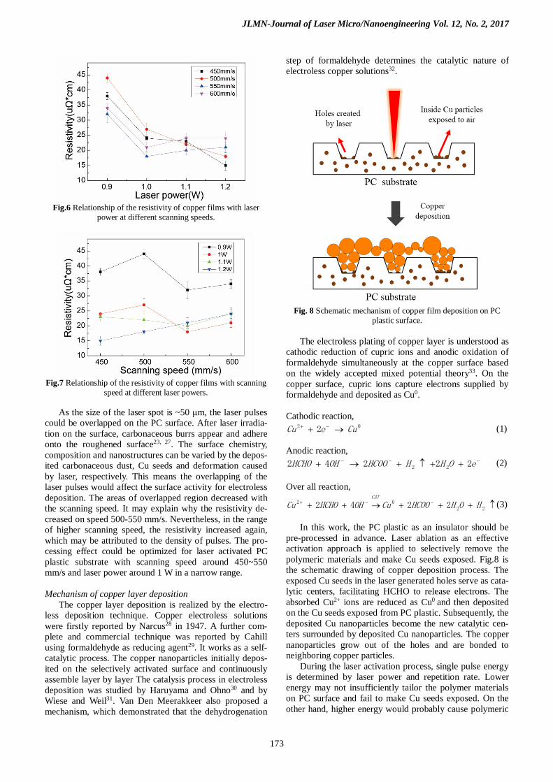
Figs.6 and 7 show the relationships among copper re-
sistivity, laser power and scanning speed. As shown in the figures, the resistivity of fabricated copper films ranges from 15 ~ 44 μΩ·cm. The lowest resistivity of 15 μΩ·cm is still 9 times higher than copper bulk (1.72 μΩ·cm, 20 ℃).However, it shows significant improved conductivi-ty compared to other groups’ research on fabricating copper tracks on non-conductive substrates with different depostion or coating methods. For example, Siyuan Qi et al. fabricated copper paste with the resistivity of 75 μΩ·cm24. Sze Kee Tam synthesized copper paste with the of resistivity 58 μΩ·cm25 and Cyuan-Jhang Wu et al syn-thesized copper paint with the resistivity of 774 μΩ·cm.
As shown in Fig.6, the peak of resistivity appears at the point of laser power = 0.9 W, scanning speed = 500 mm/s and the lowest point appears at laser power = 1.2 W and scanning speed 450 mm/s. It can be observed that the resis-tivity decreases with laser power based on the overall trend of curves. When pulsed laser is irradiated on the surface, the temperature is raised up at the interfacial zone between focusing point of laser beam and PC plastic surface, ther-mally decomposing the surface materials. As increasing laser power, it provides more thermal energy with each laser pulse, leading to faster temperature increase and larg-er heat affect zone on the focus point26. Larger heat affect zone could create larger holes and make more Cu seeds exposed. Since the Cu particles are distributed evenly on the PC plastic, laser beam with higher power could drill into deeper layers, leading to the decomposition of the pol-ymer matrix and exposing Cu seeds from subsurface layer to deliver more opportunities for metallization.
It could be observed that there exists non-monotonous trend in the figures. The resistivity first increased with the speed increased from 450 to 500 mm/s and then decreased with the speed increased from 500 to 550 mm/s and again increased with speed increased from 550 to 600 mm/s. The lowest resistivity appears at scanning speed 550 mm/s as shown in Fig.7. Estimated by scanning speed and repetition rate, the distance between each laser pulse is approximately 22.4 μm to 30 μm. The density of the laser irradiated holes decreased with the speed, indicating that less exposure of Cu seeds count against copper growth. Therefore, the resis-tivity increased at first.
JLMN-Journal of Laser Micro/Nanoengineering Vol. 12, No. 2, 2017
173
Fig.6 Relationship of the resistivity of copper films with laser
power at different scanning speeds.
Fig.7 Relationship of the resistivity of copper films with scanning
speed at different laser powers.
As the size of the laser spot is ~50 μm, the laser pulses could be overlapped on the PC surface. After laser irradia-tion on the surface, carbonaceous burrs appear and adhere onto the roughened surface23, 27. The surface chemistry, composition and nanostructures can be varied by the depos-ited carbonaceous dust, Cu seeds and deformation caused by laser, respectively. This means the overlapping of the laser pulses would affect the surface activity for electroless deposition. The areas of overlapped region decreased with the scanning speed. It may explain why the resistivity de-creased on speed 500-550 mm/s. Nevertheless, in the range of higher scanning speed, the resistivity increased again, which may be attributed to the density of pulses. The pro-cessing effect could be optimized for laser activated PC plastic substrate with scanning speed around 450~550 mm/s and laser power around 1 W in a narrow range. Mechanism of copper layer deposition
The copper layer deposition is realized by the electro-less deposition technique. Copper electroless solutions were firstly reported by Narcus28 in 1947. A further com-plete and commercial technique was reported by Cahill using formaldehyde as reducing agent29. It works as a self-catalytic process. The copper nanoparticles initially depos-ited on the selectively activated surface and continuously assemble layer by layer The catalysis process in electroless deposition was studied by Haruyama and Ohno30 and by Wiese and Weil31. Van Den Meerakkeer also proposed a mechanism, which demonstrated that the dehydrogenation
step of formaldehyde determines the catalytic nature of electroless copper solutions32.
Fig. 8 Schematic mechanism of copper film deposition on PC
plastic surface. The electroless plating of copper layer is understood as
cathodic reduction of cupric ions and anodic oxidation of formaldehyde simultaneously at the copper surface based on the widely accepted mixed potential theory33. On the copper surface, cupric ions capture electrons supplied by formaldehyde and deposited as Cu0.
Cathodic reaction,
02 2 CueCu →+ −+ (1) Anodic reaction,
−−− ++↑+→+ eOHHHCOOOHHCHO 22242 22 (2)
Over all reaction,
↑+++→++ −−+22
02 2242 HOHHCOOCuOHHCHOCuCAT
(3)
In this work, the PC plastic as an insulator should be pre-processed in advance. Laser ablation as an effective activation approach is applied to selectively remove the polymeric materials and make Cu seeds exposed. Fig.8 is the schematic drawing of copper deposition process. The exposed Cu seeds in the laser generated holes serve as cata-lytic centers, facilitating HCHO to release electrons. The absorbed Cu2+ ions are reduced as Cu0
and then deposited on the Cu seeds exposed from PC plastic. Subsequently, the deposited Cu nanoparticles become the new catalytic cen-ters surrounded by deposited Cu nanoparticles. The copper nanoparticles grow out of the holes and are bonded to neighboring copper particles.
During the laser activation process, single pulse energy is determined by laser power and repetition rate. Lower energy may not insufficiently tailor the polymer materials on PC surface and fail to make Cu seeds exposed. On the other hand, higher energy would probably cause polymeric

JLMN-Journal of Laser Micro/Nanoengineering Vol. 12, No. 2, 2017
174
materials to be burnt out. Meanwhile, the distance between holes determined by the scanning speed and repetition rate plays an important role. In the case of larger distance, the copper islands may not be able to bond to each other and the further deposition is inhibited. It is also noted that a slower scanning speed would cause laser activated region overlapped and accumulate enormous heat to make the surface damaged.
Fig.9 Adhesion testing and LED light connected to the copper
conductive tracks.
The testing of deposition layer adhesion was carried out according to GB5270-85. Firstly, a knife is used to cut the film into pieces with the size of 2 mm x 2 mm and then the tap is pasted followed by the process of quick tearing-off. It shows that the deposited copper film could not be removed by 3M tap (Scotch Magic tape 3M600). The LED emission image indicates good conductivity and adhesion of the copper films. The size of the copper lines is 1.5 mm x 8 mm and the packing of LED is 0805. 4. Conclusions
In summary, a flexible and environmental friendly method is developed to fabricate confined copper film on non-conductive modified PC plastic. Laser activation pro-cess can assist the exposure of the catalytic seeds for elec-troless deposition. The thickness of the film is about 100 µm and the resistivity of 15 μΩ·cm could be achieved by tuning the laser activation parameters. The influence of the laser power and scanning speed on film resistivity are in-vestigated. The growth mechanism of the copper film is systematically studied. A process model of the copper dep-osition is proposed to describe the dynamic process of elec-troless copper deposition, which could explain the mor-phology of copper film and its effect on electrical proper-ties. Acknowledgements
This research is supported by the National Natural Sci-ence Foundation of China (No.61605162), the National Basic Research Program of China (No.2013CBA01703), Natural Science Foundation of Fujian Province of China (No. 2017J05106) and Collaborative Innovation Center of High-End Equipment Manufacturing in Fujian. The authors also thank Stella Specialty Chemicals Pte Ltd for the sup-ply of SSC_ECU_18. References 1. A. Islam, H. N. Hansen and N. Giannekas: CIRP Ann.
Manuf. Technol., 64, (2015) 539.
2. D. H. Kim, N. Lu, R. Ma, Y. S. Kim, R. H. Kim, S. Wang, J. Wu, S. M. Won, H. Tao, A. Islam, K. J. Yu, T. i. Kim, R. Chowdhury, M. Ying, L. Xu, M. Li, H. J. Chung, H. Keum, M. McCormick, P. Liu, Y. W. Zhang, F. G. Omenetto, Y. Huang, T. Coleman and J. A. Rogers: Science, 333, (2011) 838.
3. T. Sekitani, T. Yokota, U. Zschieschang, H. Klauk, S. Bauer, K. Takeuchi, M. Takamiya, T. Sakurai and T. Someya: Science, 326, (2009) 1516.
4. T. Leneke, H. Soeren and B. Schmidt: ESTC, (2008) 663.
5. M. F. Shafique, K. Saeed, D. P. Steenson and I. D. Robertson: IEEE Trans. Microwave Theory Tech., 57, (2009) 3254.
6. P. Amend, C. Pscherer, T. Rechtenwald, T. Frick and M. Schmidt: Physics Procedia, 5, (2010) 561.
7. S. M. Huang, M. H. Hong, Y. F. Lu, B. S. Lukỳanchuk, W. D. Song and T. C. Chong: J. Appl. Phys., 91, (2002) 3268.
8. M. Calaon, A. Islam, H. N. Hansen and C. Ravn: Int. J. Adv. Manuf. Technol., 59, (2012) 101.
9. S. C. Huang, T. C. Tsao and L. J. Chen: J. Electrochem. Soc., 157, (2010) D222.
10. P. Balaramesh: Int. J. Innov. Res. Stud., 3(4), (2014) 167.
11. J. Kim, S. H. Wen, D. Y. Jung and R. W. Johnson: IBM J. Res. Dev., 28, (1984) 697.
12. X. Cui, D. A. Hutt and P. P. Conway: Thin Solid Films, 520, (2012) 6095.
13. G. A. Krulik: J. Chem. Educ., 55(6), (1978) 361. 14.Y. Zhang, H. N. Hansen, A. De Grave, P. T. Tang and J.
S. Nielsen: Int. J. Adv. Manuf. Technol., 55, (2010) 573. 15. T. C. Chong, M. H. Hong and L. P. Shi: Laser
Photonics Rev., 4, (2010) 123. 16. M. H. Hong, S. M. Huang, B. S. Luk’yanchuk and T. C.
Chong: Sens. Actuators, A, 108, (2003) 69. 17. M. Paunovic: J. Electrochem. Soc., 130, (1983) e309. 18.F. Inoue, H. Philipsen, A. Radisic, S. Armini, Y. Civale,
S. Shingubara and P. Leunissen: J. Electrochem. Soc., 159, (2012) 4.
19. L. Bauer: Offline Programming of 3D Laser Systems, 2787, (1996) 34.
20. M. Fanhui and W. Hongzhi: 11th International Conference on Electronic Packaging Technology & High Density Packaging (ICEPT-HDP), (2010) 902.
21. U. S. Pat., U. S. 6,319,564.20, (2001). 22. M. A. Roberts, J. S. Rossier, A. Paul Bercier and H.
Girault: Anal. Chem., 69, (1997) 2035. 23. F. Caiazzo, F. Curcio, G. Daurelio and F. M. C.
Minutolo: J. Mater. Process. Technol., 159, (2005) 279. 24. S. Qi, R. Litchfield, D. A. Hutt, B. Vaidhyanathan, C.
Liu, P. Webb and S. Ebbens: IEEE 62nd Electronic Components and Technology Conference, (2012) 1651.
25. S. K. Tam and K. M. Ng: J. Nanopart. Res., 17, (2015) 1.
26. A. K. Ghavidel, M. Shabgard and H. Biglari: J. Appl. Polym. Sci., 133, (2016) 1.
27. P. A. Atanasov: Proc. SPIE Int. Soc. Opt. Eng., 3092, (1997) 772.
28. H. Narcus: Met. Finish., 45, (1947) 964. 29. A. E. Cahill: Am. Electrochem. Soc. Proc., 44, (1957)
130.

JLMN-Journal of Laser Micro/Nanoengineering Vol. 12, No. 2, 2017
175
30. I. O. S. Haruyama: Electroless Deposition of Metals and Alloys, 12, (1988) 20.
31. H. Wiese: Electroless Deposition of Metals and Alloys, 12, (1988) 53.
32.V. D. Meerakker: J. Appl. Electrochem., 11, (1981) 395. 33. M. Paunovic: Plating, 55, (1968) 1161. (Received: April 25, 2017, Accepted: September 3, 2017)


![Electroless plating of rhenium-based alloys with nickel ...neliaz/Papers_Files/J94.pdf · vapor deposition (CVD) and electroplating [6–17] . The electroless deposition process may](https://static.fdocuments.us/doc/165x107/5e437680bca32e632013b637/electroless-plating-of-rhenium-based-alloys-with-nickel-neliazpapersfilesj94pdf.jpg)