Electroless Cu Plating Microelectronics Applications · Anodic oxidation of Zinc 2. Cathodic...
91
1 Electroless Cu Plating Microelectronics Electroless Cu Plating Microelectronics Applications Applications Prof. Yosi Shacham-Diamand
-
Upload
dinhkhuong -
Category
Documents
-
view
229 -
download
2
Transcript of Electroless Cu Plating Microelectronics Applications · Anodic oxidation of Zinc 2. Cathodic...

1
Electroless Cu Plating Microelectronics Electroless Cu Plating Microelectronics ApplicationsApplications
Prof. Yosi Shacham-Diamand

2
Cross section of ULSI interconnect scheme (ITRS 2001)
Hierarchical Scaling
3
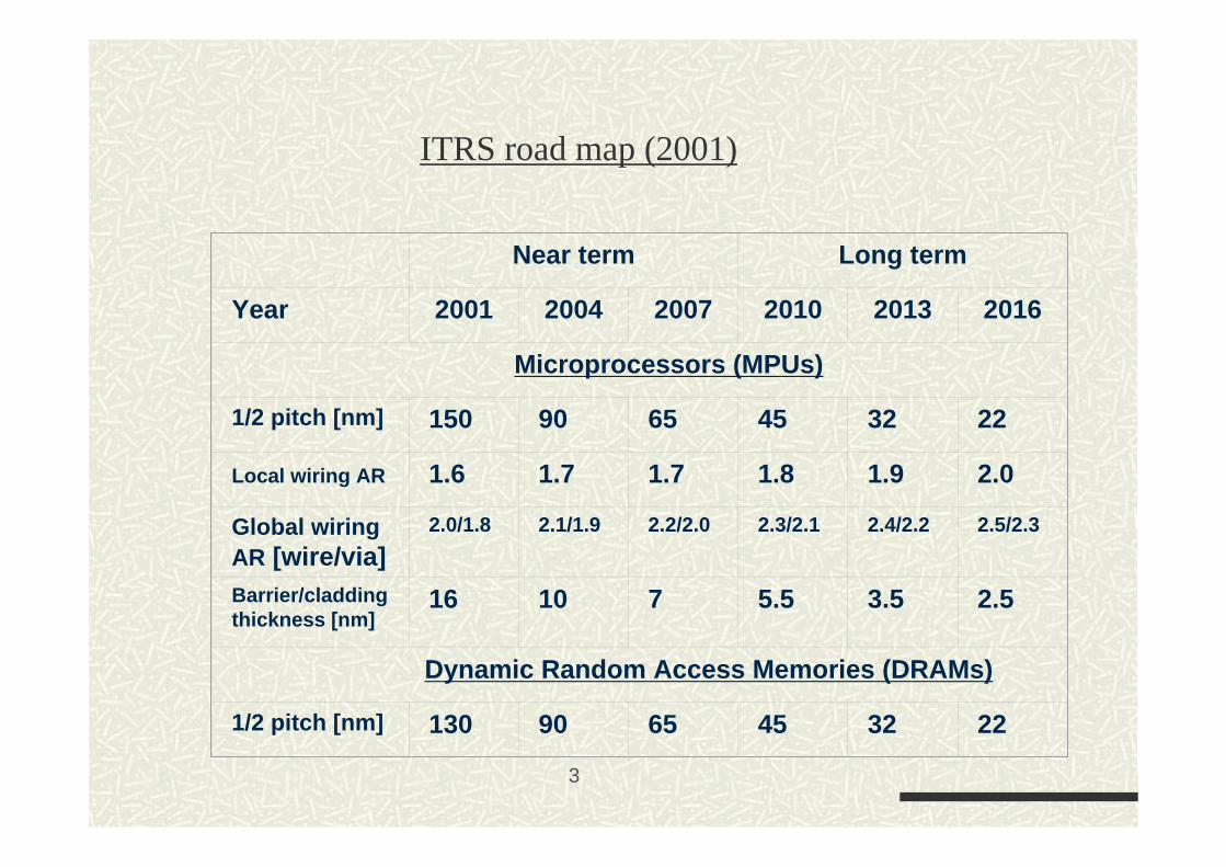
ITRS road map (2001)
Near term Long term
Year 2001 2004 2007 2010 2013 2016
Microprocessors (MPUs)
1/2 pitch [nm] 150 90 65 45 32 22
Local wiring AR 1.6 1.7 1.7 1.8 1.9 2.0
Global wiring AR [wire/via]
2.0/1.8 2.1/1.9 2.2/2.0 2.3/2.1 2.4/2.2 2.5/2.3
Barrier/cladding thickness [nm]
16 10 7 5.5 3.5 2.5
Dynamic Random Access Memories (DRAMs)
1/2 pitch [nm] 130 90 65 45 32 22

4
Sub-100 nm interconnects (a)
Problems:Materials properties – texture, morphologyProcess – coverage, uniformity.Integration – compatibility, integrabilityTools – new processes require new toolsResistivity – dimension effects: Narrow Line
Resistivity Increase (NLRI) effectReliability: voiding, delamination, electromigration, corrosionHigh complexity, large chips with high lead counts packaging
All this lead to long learning time, high NRE, low yield and eventually, to cost problems

5
Sub-100 nm interconnects (b)
Solutions:Better deposition methods – ALD, seedless electrolessClever integration methods - Integrated barrierAlloying –.
Conducting metal - barrier-less metallization, better conductivity for sub-50 nm linesBarriers: Better materials. e.g. Co(W,P) is a better barrier than Co(P), electroless barriers offer high selectivity and save process steps
6
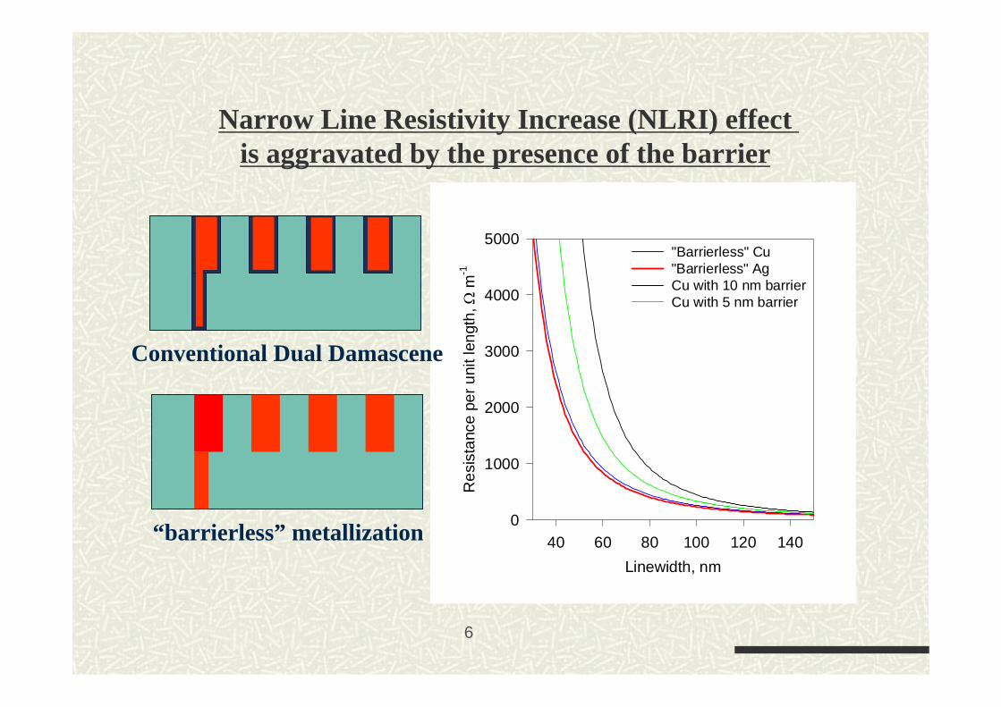
Narrow Line Resistivity Increase (NLRI) effect is aggravated by the presence of the barrier
Linewidth, nm40 60 80 100 120 140
Res
ista
nce
per u
nit l
engt
h, Ω
m-1
0
1000
2000
3000
4000
5000"Barrierless" Cu "Barrierless" Ag Cu with 10 nm barrierCu with 5 nm barrier
“barrierless” metallization
Conventional Dual Damascene
7
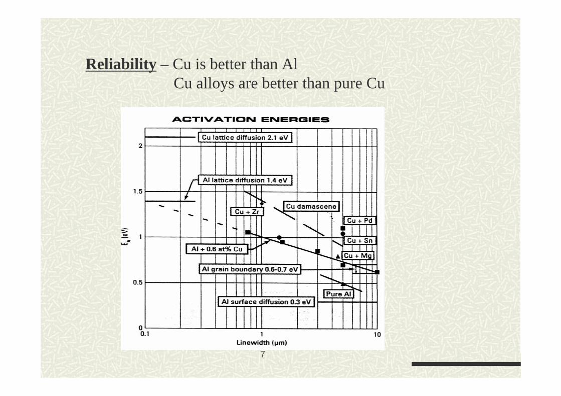
Cu is better than Al–ReliabilityCu alloys are better than pure Cu

8
Cu technology main problemsCu technology main problems
Difficult to EtchPoor Adhesion to dielectricsRapid Diffusion through SiO2 and low-K
inter-level-dielectrics (ILD)Forms mid-gap energy level in SiVia/trench fillingPost CMP damageCorrosion

9
Electroless Plating of Copper

10

11
Standard redox potential for components for electroless Cu plating

12
Components of ELS Cu baths

13
Metal displacement reactionExample: when Zinc is immersed in a Copper Sulfate solution:
V 0.76E 2 020 =+→ −+ eZnZn
V 0.34-E 2 002 =→+ −+ CueCu
1. Anodic oxidation of Zinc
2. Cathodic reduction of Cu
Result:
Cu is deposited on the Zn sample
After all the Zn sample is coated with Cu the deposited stops.
E0 = 0.76 (Oxidation)
E0 = +0.34 (Reduction)

14
Pourbaix Diagram for Cu

15
Pourbaix diagram for carbon-water
16
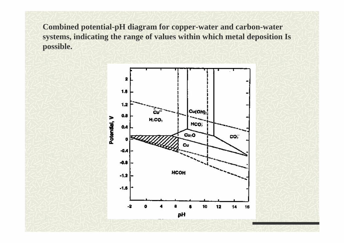
Combined potential-pH diagram for copper-water and carbon-water systems, indicating the range of values within which metal deposition Is possible.

17
Nernst equation
E0 – the potential versus a standard hydrogen electrode (SHE)
Note that E0 is defined for the standard RedOx reaction
[ ][ ]d
OxnFRTdneOx Re
0 lnEE Re +=→+ −
Therefore E0 is defined for [Ox]=[Red]=1M
E is the RedOx potential; it is related to the free energy change of the reaction as
∆G=-nqE

18
Electroless plating solution1. Cu salt – Cu is reduced
Cu+2 + 2e- Cu0 E0Cu = 0.34 eV
2. Reducing agent – oxidized at the interface
Red-n Red-n+2 + 2e- Oxidation potential = -Ered
(Red-n+2 + 2e- Red-n , -Ered < Ecu
3. Total reaction – Cu+2 + Red—n Cu0 + Red-n+2
∆E= ECu+ Ered >0 ∆G=-2q∆E < 0,
i.e. spontaneous deposition !!!
19
Typical Cu electroless deposition solutions

20
Component Aim Cu deposition
Metal salt metal ion source CuSO4•5H2O
Reducing agent reducing the metal ion HCOH
Complexing agent reducing electrochemical potential difference
EDTA
pH adjustments electrochemical potential, rate and mechanism
N(C2H5)4OH,
Stabilizer stabilizing the solution, preventing hydrogen inclusion
N(CH3)4CN 2,2'-dipyridyl
Surfactant reducing surface tension, extracting H2
RE-610
Electroless Cu for VLSI metallization

21
IBM bath (Example):T= 65°C pH=8-10Dipyridyl (100 pprn), Tetraazadodecane (0.04 M),Triethanolamine (0.3 M), and Dimethylamine borane (0.067 M).

22
Cu electroless deposition solution

23
Cu electroless deposition solution

24
Electroless copper plating (Kohl 03)
0.04M copper sulfate, 0.0057M nickel sulfate, 0.28M sodium hypophosphite,0.051M sodium citrate, 0.485M boric acid,250 ppm accelerators (formamidine disulfide)0–50 ppm 2,2-dipyridyl. Deionized water was used to prepare the solutions. pH = 9.0–9.3. (Adjusted with NaOH and H2SO4)Temperature = 70 ± 0.5 .C.

25
Effect of 2,2’ - dipyridyl

26
Effect of 2,2’ - dipyridyl
XRD patterns of copper deposits from different 2,2-dipyridyl concentration bath: (a) 0 ppm; (b) 20 ppm; (c) 40 ppm.

27
Effect of 2,2’ - dipyridylResistivity of the copper deposits: dependence of the resistivity of copper deposits on 2,2-dipyridyl concentration
The dependence of copper deposit resistivity (20 ppm 2,2-dipyridyl) on annealing temperature.
28
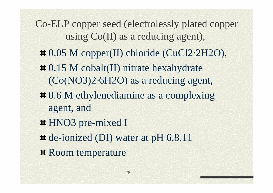
Co-ELP copper seed (electrolessly plated copper using Co(II) as a reducing agent),
0.05 M copper(II) chloride (CuCl2·2H2O), 0.15 M cobalt(II) nitrate hexahydrate(Co(NO3)2·6H2O) as a reducing agent, 0.6 M ethylenediamine as a complexingagent, and HNO3 pre-mixed Ide-ionized (DI) water at pH 6.8.11 Room temperature

29
HCHO-ELP copper seed (electrolessly plated copper using para-formaldehyde as a reducing agent)
0.03 M copper sulfate (CuSO4·5H2O), 0.05 M ethylenediaminetetraacetic acid (EDTA), 0.1 M para-formaldehyde (HCHO) as a reducing agentand RE-610 as a surfactant pH 13 based on KOH.10 Room temperature.
30
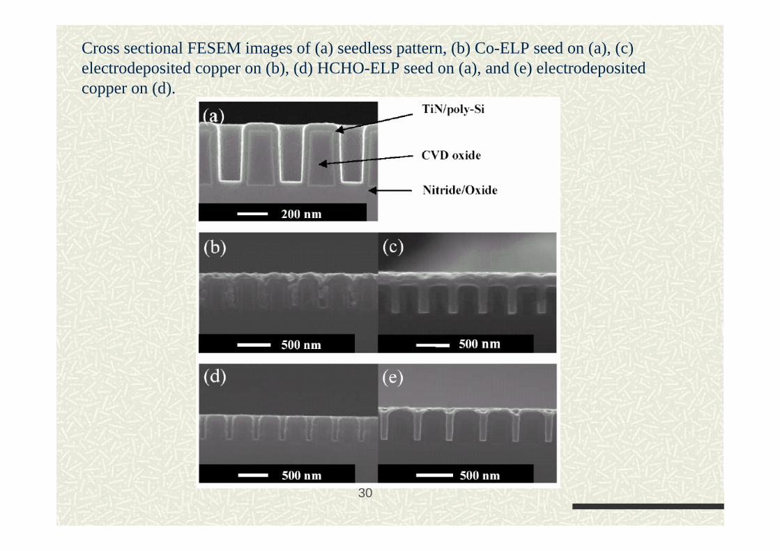
Cross sectional FESEM images of (a) seedless pattern, (b) Co-ELP seed on (a), (c) electrodeposited copper on (b), (d) HCHO-ELP seed on (a), and (e) electrodeposited copper on (d).

31
Catalytic activities of metals (the potentials at 10 ' Ncm') for anodic oxidation of different reductants. EN = oxidatlon-reduction potentials of reductants. H2 = reversible hydrogen potentials. Conditions: (a) 0.2M NaH2P02 + 0.2M Na-citrate + 0.5M HIBQt, pH 9.0, 343 K; (b) 0.1M HCHO +0.175M EDTA.2Na, pH 12.5,298 K; (c) 0.03M NaBH, +0.175M EDTA.2Na, pH 12.5,298 K (d 2.0 g/dm' DMAB + 0.2M Na-citrate = 0.5M HIBO1, pH 7.0,298 K (e) 1.OM N?H, + 0.175M EDTA,2Na, pH 12.0, 298 K.

32
ELS Cu on W: Potential versus pH diagram for the tungsten-water system showing regions of thermodynamic stability for passivation,
corrosion, and immunity.
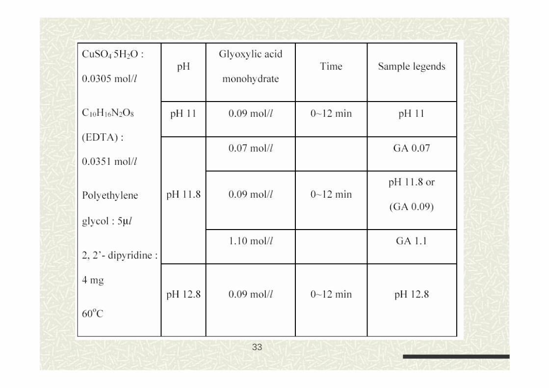
33

34
X-ray diffraction of Cu films versus solution of pH (fixed glyoxylic acid 0.09 mol/l, 60 C, 10 min).

35
X-ray diffraction of Cu films versus glyoxylic acid molar concentration (fixed pH 11.8, 60C, 8 min).

36
Mixed potential model

37
I [A]
Electroless solution potential, V
Oxidation of the reducer
ia
Ic Reduction of the metal ions
E0Mz+
E0red
Mixed potential
Emp
Total current
In electroless plating the total current = 0
Therefore, the anodic current balances the cathodic current

38

39
A schematic Evan’s diagram showing the two partial processes of the additive copper bath.

40
dcba LigandHCOHOHCukRate ][][][][ 2 −−=
6. S.M. El-Raghyand A.A. Aho-Solama, J. Electrochem. Soc., 126,171 (1979).8. A. Molenaar, M.F.E. Holsrinet and L.K.H. van Beek, Plating, 61,238 (1974).22. F.M. Donahue, K.L.M. Wongand R. Bhalla, J. Electrochem. Soc., 127,234023. J. Dumesic, J.A. Koutsky and T.W. Chapman, ibid., 121, 1405 (1974).56. F.L. Shippey and F.M. Donahue, Plating, 60,43 (1973).

41
Mass transfer effects:interfacial (surface) concentrations differ from
bulk concentrations ::
xxbx D
FluxCC δ⋅⋅−= 3
, 10

42

43
Cu dep. Rate vs pH (Cu2+, HCOH solution)

44
pH and Temperature effect:
Tartarte bath:5 g/l CuSO4, 25 g/l K–Na tartarate salt, 5–10 g/l NaOH10 ml/l formaldehyde,
EDTA bath5 g/l CuSO4, 30 g/l EDTA, 10–15 g/l NaOH15 ml/l formaldehyde.

45
Additive effects

46
Additive effects: EDTA bath

47
Additive effects: EDTA bath

48
Additive effects: tartarate bath

49
Additive effects: tartarate bath

50
Cu Hypophsphite bath
24 mM (millimolar) CuSO,52 mM sodium citrate, 2 mM NiSO,100 mM sodium hypophosphite, 150 mM boricpH = 9.2 with NaOH, Bath temperature of 65°C. Activation with NiSO4

51
Cu Hypophsphite bath
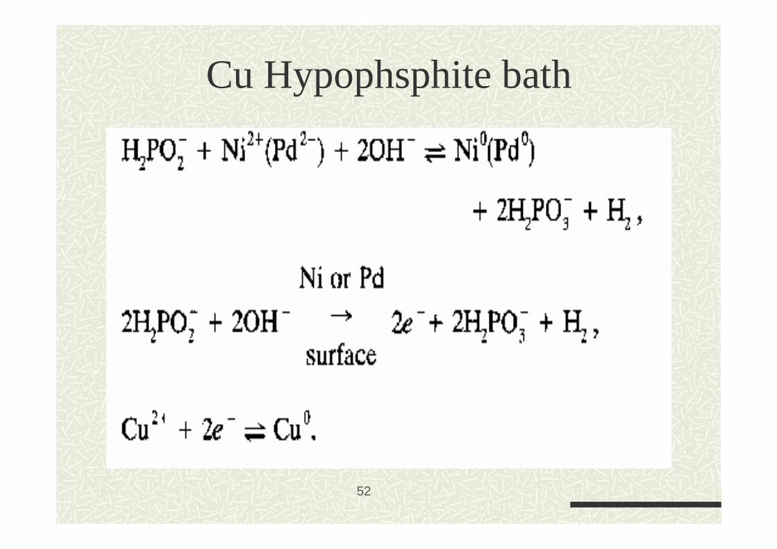
52
Cu Hypophsphite bath

53
Effect of temperatures on plating rate in additive-free electroless baths.

54
Effect of pH

55
reducing agents for Electroless Cu
formaldehyde, hypophosphite , borohydride , hydrazine, di-methylamine borane (DMAB), glyoxylic acid redox-pairs (i.e. Fe(II)/Fe(III), Ti(III)/Ti(IIII), Cr(II)/Cr(III), V(II)/V(III))
.

56
Complexing agents for electroless Cu
Ethylenediaminetetraacetic acid (EDTA), malicacid (Mal), succinic acid (Sue), tartrate (Tart), citrate(Cit), triethanolamine (TEA) Ethylenediamine (En)
57
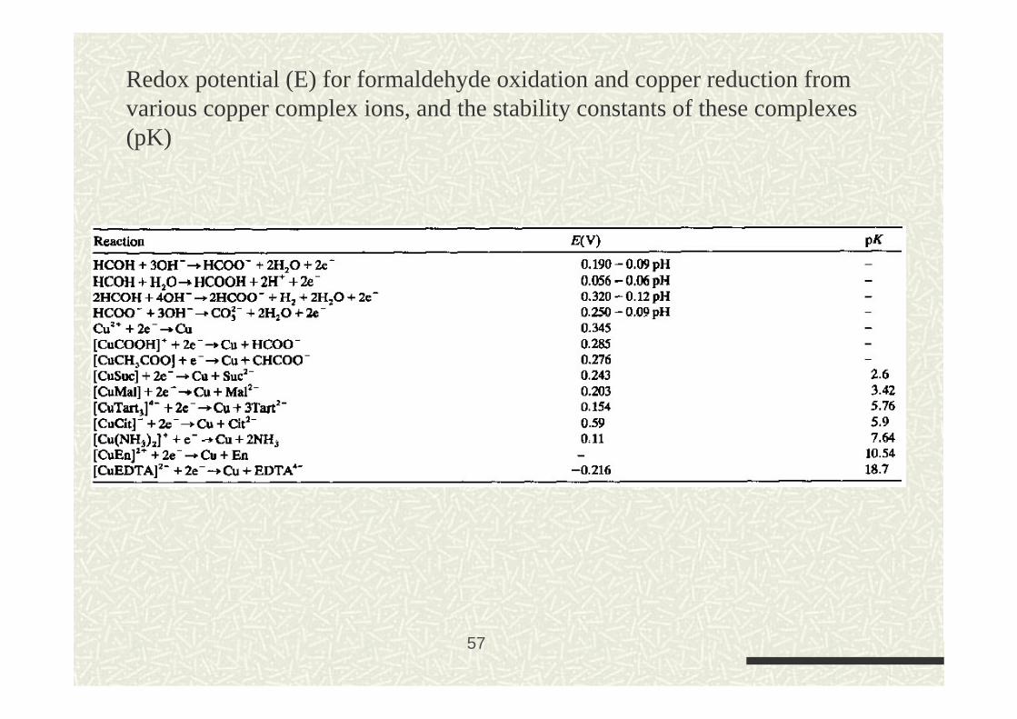
Redox potential (E) for formaldehyde oxidation and copper reduction from various copper complex ions, and the stability constants of these complexes (pK)

58
Anodic partial reaction

59
60
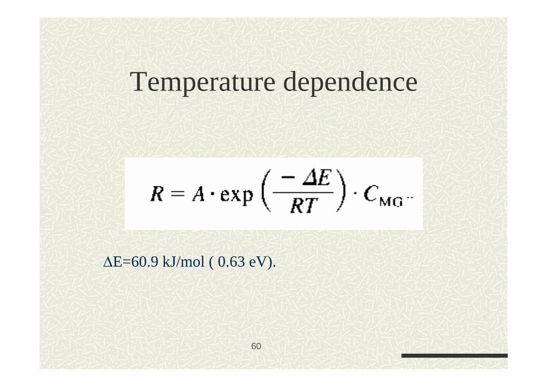
Temperature dependence
∆E=60.9 kJ/mol ( 0.63 eV).

61
Electroless Cu deposition process

62
Solution for contact displacement copper deposition on TiN

63
Electroless Cu deposition rate and resistivity vs. deposition solution parameters
64
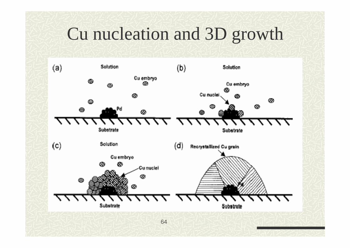
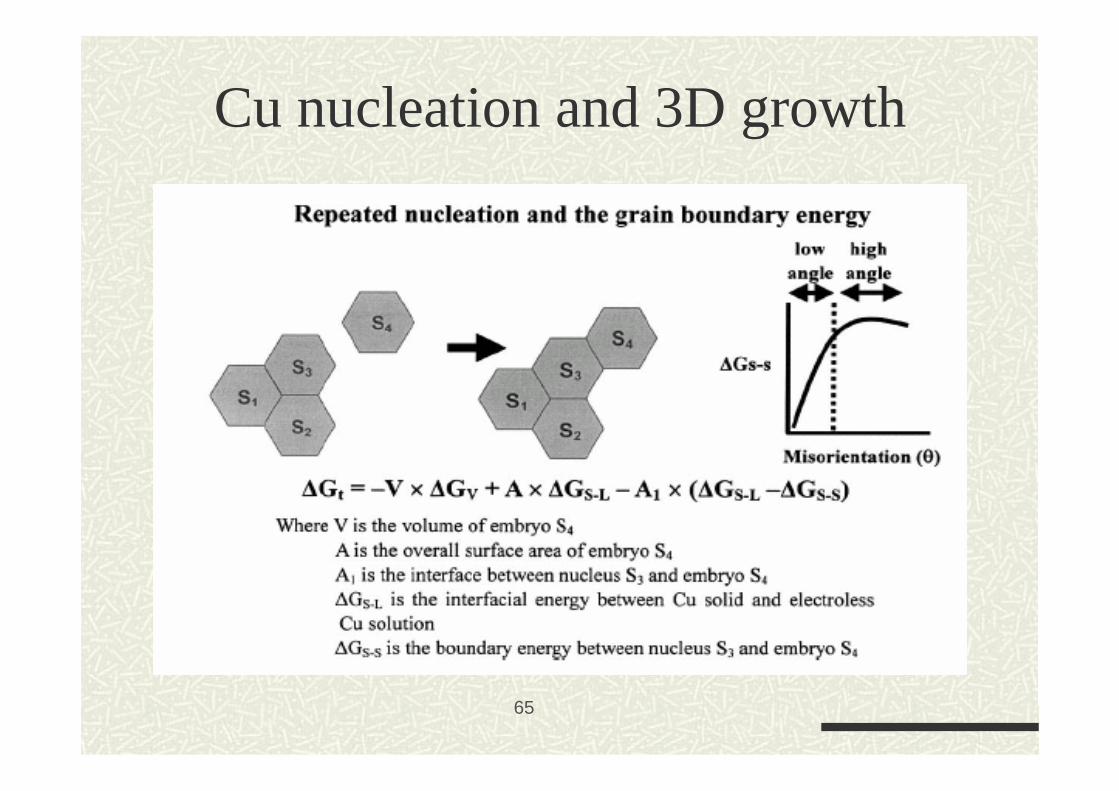
Cu nucleation and 3D growth
65
Cu nucleation and 3D growth

66
Cu ions diffusivity study
SEM picture of the entrance to a 0.7 µm high, 10 µm wide micro-tunnel (a) and the schematic picture showing themicro-tunnel entrance and the seed layer (b).

67
Cu ions diffusivity study
D is the copper ions' diffusivity,
R is the deposition rate,
h is the tunnel height, and
Ω is the Cu density

68
Copper thickness versus distance from the entrance of a 150 µm long micro-channel. The deposition conditions were: T=40°C, CuS04--25 mg/l, HCHO--1 ml/l, RE610~7.5 ml/1, and KCN---1 mg/1.
D=10-6-10-5 cm2/sec

69
Electroless Cu with Glyoxilic acid
( ) ( )[ ]adsads OOHCHOHHCOH −− ↔+ 2
( )[ ] −− ++↔ eHHCOOHOOHCH ads 22 21
The activity of formaldehyde in electroless deposition is due tothe high reactivity of the carbonyl group –COH. The carbon-oxygen double bond, C=O, is formed by both σ and π orbitals. Therefore, the C=O bond can be oxidized to form a carboxyl COOH group. In the case of formaldehyde the following reaction takes place in high pH solution:

70
List of aldehydes under investigation
None1. Sugars ( Sucrose, Maltose, Dextrose, Fructose, Glucose)
None1. Glutaraldehyde (50% sol.)
None1. Glyoxale C2H2O2
Good1. Glyoxylic acid (formylformic acid)
None1. Propionaldehyde
Medium1. Acetaldehyde (50% sol.)
Good1. Formaldehyde (37% sol.)
Reducing capabilityChemicals studied

71
Solution composition for electroless Cu deposition with glyoxylic acid
Adjust pH to 12.3-12.7KOH
0.004 g/lSurfactant RE-610
0.054 – 0.11 MGlyoxylic acid
0.0351 MEDTA
0.0305 MCuSO4·5H2O
ConcentrationComponents

72
Deposition rates of electroless copper from solutions with glyoxylic acid.
90Pd activated Si30 gr. / l glyoxylic acid
66Pd activated Si15 gr. / l glyoxylic acid
62.5Sputtered Co15 gr. / l glyoxylic acid
Dep. Rate [nm/min]SubstrateSolution

73
C u film thickness, [A ]0 500 1000 1500 2000 2500 3000 3500 4000
Res
istiv
ity o
f Cu
film
s [O
hm-c
m]
0.0e+0
1.0e-6
2.0e-6
3.0e-6
4.0e-6
5.0e-6
6.0e-6
7.0e-6As deposited A fter 200C anneal

74

75
Solution composition for electroless Cu deposition with Glyoxylic acid
Components Concentration
CuSO4·5H2O 0.0305 M
EDTA 0.0351 M
Glyoxylic acid 0.054 – 0.11 M
Surfactant RE-610 0.004 g/l
KOH or TMAH Adjust pH to 12.3-12.7

76
ab
cSEM pictures of via contacts (a) before
deposition (with seed layer), (b) after 1 min
electroless copper film deposition, and (c) after 2
minutes of ELD Cu.

77
Electroless deposition of alloys is also possible for VLSI applications…..

78Source: J.A. Cunningham, SI, April 2000
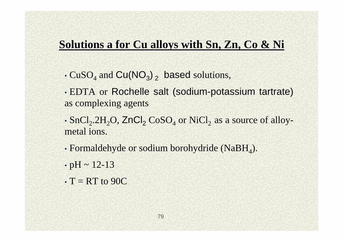
79
, Zn, Co & Ni, Zn, Co & NiSnSnSolutions a for Cu alloys with Solutions a for Cu alloys with
• CuSO4 and Cu(NO3) 2 based solutions,
• EDTA or Rochelle salt (sodium-potassium tartrate) as complexing agents
• SnCl2.2H2O, ZnCl2 CoSO4 or NiCl2 as a source of alloy-metal ions.
• Formaldehyde or sodium borohydride (NaBH4).
• pH ~ 12-13
• T = RT to 90C

80
Thickness of electroless deposited thin films (A)
0 200 400 600 800 1000 1200 1400
Elec
trol
ess
depo
site
d th
in fi
lms
resi
stiv
ity, Ω
.cm
1e-5
1e-4
1e-3
CuCo/Co CuNi/Co
Resistivity of electroless Cu-Co & Cu-Ni as a function of film thickness

81
Molar ratio [Cu++]/[Ni++] in bath
0.00 .05 .10 .15 .20 .25 .30 .35 .40
Res
istiv
ity o
f ele
ctro
less
dep
osite
dth
in C
u-N
i film
s, Ω
.cm
0e+0
1e-6
2e-6
3e-6
4e-6
5e-6
6e-6
7e-6
8e-6
9e-6
1e-5on Cu as depositedon Co as depositedon Cu(2500C) on Co(2500C)
Resistivity of Cu-Ni films as a function of The molar ratio [Ni++]/[Cu++]

82
FIB/SEM images of feature fill of 0.18 µm · 1.1 µm, 6:1 aspectratio vias with 300 A PVD Ta barrier and 500 A PVD Cu seed.Electroless Cu was deposited on the PVD Cu seed to thickness values of 0, 75, 125, 175 A followed by electroplating of 0.25 µm of copper.

83
TEM micrograph of electroless-plated Cu trench in 15 nm TaNfilm after annealing

84
Cross-sectional SEM micrographs of electroless Cu deposition profiles for various plating times. Via hole diameter and depth were 0.4 and 2.3 µm. Additives: SPS ~0.5 mg/L andPEG ~molecular weight 4000; 0.5g/L. pH 12.5; temperature 70°C.

85
-Cross-sectional TEM micrograph of a 100 nm via hole filled with electroless plated Cu. - 1 nm ICB-Pd catalyst layer was used. - Deposition time: 2 min. - Additives:
-SPS ~0.5 mg/L and - PEG ~MW 4000, 0.5 g/L.
- 12.5; - temperature 70°C.

86
ELS Process integration schemes

87
“Almost” Full electrioless process
Pre-deposition cleanActivation process (Pd, non-Pd)Electroless deposition step 1 – Fast and dense nucleation on the PVD barrier, no deposition on the ILDAnneal in vacuum (Optional)Electroless deposition step II – superfillingCMP + Post CMP cleanElectroless capping

88
Full electrioless process1st Pre deposition cleanActivation ELS barrier2nd Pre-deposition clean Electroless deposition step 1 – Fast and dense nucleation on the PVD barrier, no deposition on the ILDAnneal in vacuum (Optional)Electroless deposition step II – super-fillingCMP + Post CMP cleanElectroless capping

89
1µm Cu/ 10nm Cu seed (PVD)
1µm Cu/ 12nm Cu seed (ELS)/ 10 nm Cu (PVD

90
Glyoxilic bath aging

91
Summary
•ELS Cu I as good as electroplated Cu for VLSI applications
• Resistivity <2 µΩ.cm
• Very high selectivity
• Penetrates sub-100 nm features
• Can deposit on sub 10 nm features.