ELECTRODEPOSITION OF METAL ON GALLIUM ARSENIDE...
102
ELECTRODEPOSITION OF METAL ON GALLIUM ARSENIDE NANOWIRES by Chao Liu B.Sc., Shandong Normal University, 2008 A THESIS SUBMITTED IN PARTIAL FULFILLMENT OF THE REQUIREMENTS FOR THE DEGREE OF MASTER OF SCIENCE In the Department of Physics Faculty of Science © Chao Liu 2011 SIMON FRASER UNIVERSITY Summer 2011 All rights reserved. However, in accordance with the Copyright Act of Canada, this work may be reproduced, without authorization, under the conditions for Fair Dealing. Therefore, limited reproduction of this work for the purposes of private study, research, criticism, review and news reporting is likely to be in accordance with the law, particularly if cited appropriately.
Transcript of ELECTRODEPOSITION OF METAL ON GALLIUM ARSENIDE...

ELECTRODEPOSITION OF METAL ON GALLIUM
ARSENIDE NANOWIRES
by
Chao Liu
B.Sc., Shandong Normal University, 2008
A THESIS SUBMITTED IN PARTIAL FULFILLMENT OF
THE REQUIREMENTS FOR THE DEGREE OF
MASTER OF SCIENCE
In the
Department of Physics
Faculty of Science
© Chao Liu 2011
SIMON FRASER UNIVERSITY
Summer 2011
All rights reserved. However, in accordance with the Copyright Act of Canada, this work
may be reproduced, without authorization, under the conditions for Fair Dealing.
Therefore, limited reproduction of this work for the purposes of private study, research,
criticism, review and news reporting is likely to be in accordance with the law,
particularly if cited appropriately.
ii
APPROVAL
Name: Chao Liu
Degree: Master of Science
Title of Thesis: Electrodeposition of Metal on Gallium Arsenide
Nanowires
Examining Committee:
Chair: Dr. J. Steven Dodge
Associate Professor, Physics
__________________________________________
Dr. Karen Kavanagh
Senior Supervisor
Professor, Physics
__________________________________________
Dr. Simon Watkins
Supervisor
Professor, Physics
__________________________________________
Dr. Patricia Mooney
Supervisor
Professor, Physics
__________________________________________
Dr. Erol Girt
Internal Examiner
Associate Professor, Physics
Date Defended/Approved: June 27, 2011
iii
ABSTRACT
In the majority of reported studies, metal contacts to semiconductor nanowires
(NWs) have been fabricated using high-resolution electron-beam lithography with metal
evaporation. In our study, copper (Cu) or iron (Fe) electrical contacts to as-grown gallium
arsenide (GaAs) nanowires have been fabricated via electrodeposition. For nominally
undoped GaAs nanowires, we find that Cu or Fe has a preference for nucleation and
growth on the gold catalyst avoiding the sidewalls. For carbon-doped nanowires with
higher conductivity, Cu nucleation and growth began to occur on the sidewalls as well as
on the gold catalyst. COMSOL finite element analysis, carried out to simulate the
experimental results, was used to discuss the growth mechanism in terms of nanowire
sample surface, conductivity and morphology.
Keywords: nanowire; electrodeposition; GaAs; conductivity

iv
DEDICATION
心随野鹤白云外,
梦卧宙宇千年间.
Hello World, I am coming.
L.Y.C @ 2011
v
ACKNOWLEDGEMENTS
First and foremost I would like to thank my senior supervisor, Dr. Karen Kavanagh, who
has supported and encouraged me throughout my graduate career. My first project did not
go well for the first year, Dr. Kavanagh proposed this new project idea and provided lots
of valuable academic insights and editorial comments during the research. I especially
thank her for providing me opportunities to present my work at international conferences,
helping me improve my English and presentation skills.
I would also like to thank Dr. Simon Watkins and his graduate student Omid
Salehzadeh Einabad, for their collaboration, support and scientific suggestions regarding
my work. This work could not be done without their constant supply of experimental
samples.
I would also like to acknowledge past and present members of the Kavanagh lab,
Dr. Zhiliang Bao and Dr. Wenjie Li, especially Sarmita Majumder, who offered helpful
guidance and taught me to be patient and careful for the electrodeposition experiment.
I also thank Dr. Patricia Mooney and Dr. Erol Girt, for the valuable discussion
about trend and lifestyle in academia and industry. Finally, I would like to thank my close
friends and family, in Canada and China, who were always there to encourage me.
I am grateful to the Physics department, as a small and comfort community,
provided me a memorable learning experience and I do enjoy my days in SFU physics.

vi
My dream is to build a high-tech company before I turn 35, the graduate study experience
will help me along the way chasing my dreams.
vii
TABLE OF CONTENTS
Approval ................................................................................................................................ ii
Abstract ................................................................................................................................ iii
Dedication ............................................................................................................................ iv
Acknowledgements ................................................................................................................ v
Table of Contents ................................................................................................................. vii
List of Figures ....................................................................................................................... ix
List of Tables ....................................................................................................................... xii
Introduction ......................................................................................................................... 1
1: Electrodeposition ............................................................................................................. 3
1.1 Electrodeposition overview ............................................................................................ 3
1.1.1 Nernst’s equation and overpotential .................................................................... 4 1.1.2 Butler-Volmer equation ..................................................................................... 5
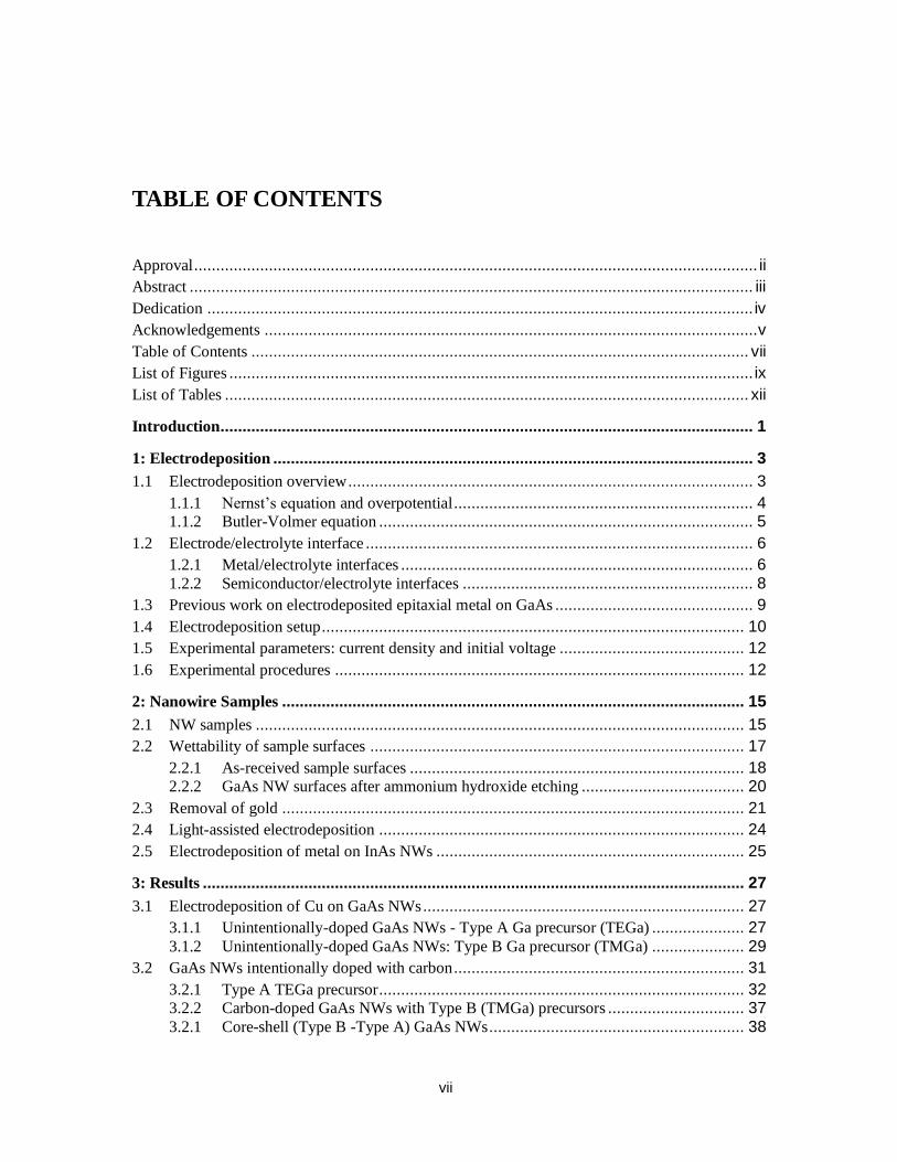
1.2 Electrode/electrolyte interface ........................................................................................ 6
1.2.1 Metal/electrolyte interfaces ................................................................................ 6 1.2.2 Semiconductor/electrolyte interfaces .................................................................. 8
1.3 Previous work on electrodeposited epitaxial metal on GaAs ............................................. 9
1.4 Electrodeposition setup ................................................................................................ 10
1.5 Experimental parameters: current density and initial voltage .......................................... 12
1.6 Experimental procedures ............................................................................................. 12
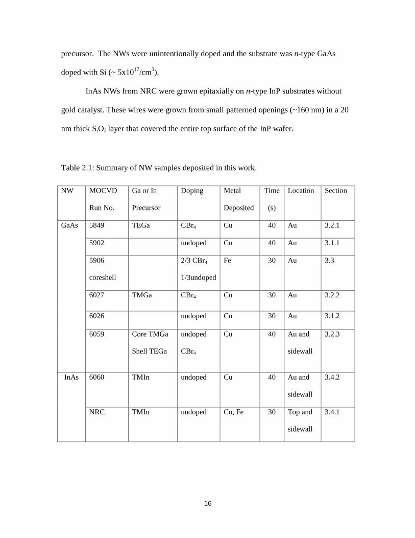
2: Nanowire Samples ......................................................................................................... 15
2.1 NW samples ............................................................................................................... 15
2.2 Wettability of sample surfaces ..................................................................................... 17
2.2.1 As-received sample surfaces ............................................................................ 18 2.2.2 GaAs NW surfaces after ammonium hydroxide etching ..................................... 20
2.3 Removal of gold ......................................................................................................... 21
2.4 Light-assisted electrodeposition ................................................................................... 24
2.5 Electrodeposition of metal on InAs NWs ...................................................................... 25
3: Results ........................................................................................................................... 27
3.1 Electrodeposition of Cu on GaAs NWs ......................................................................... 27
3.1.1 Unintentionally-doped GaAs NWs - Type A Ga precursor (TEGa) ..................... 27 3.1.2 Unintentionally-doped GaAs NWs: Type B Ga precursor (TMGa) ..................... 29
3.2 GaAs NWs intentionally doped with carbon .................................................................. 31
3.2.1 Type A TEGa precursor ................................................................................... 32 3.2.2 Carbon-doped GaAs NWs with Type B (TMGa) precursors ............................... 37 3.2.1 Core-shell (Type B -Type A) GaAs NWs .......................................................... 38

viii
3.3 Electrodeposition of Fe on GaAs nanowires .................................................................. 40
3.4 Electrodeposition of metal on InAs nanowires ............................................................... 45
3.4.1 NRC InAs NWs .............................................................................................. 45 3.4.2 Electrodeposition of Cu on InAs NWs from Dr. Watkins’ group ........................ 49
3.5 Experiment with light illumination ............................................................................... 49
3.6 Metal deposition without gold catalyst .......................................................................... 50
3.6.1 Electrodeposition of Cu on gold nanoparticle samples ....................................... 50 3.6.2 Cu growth without gold catalyst ....................................................................... 51
4: Discussion ...................................................................................................................... 56
4.1 Current and resistivity calculation ................................................................................ 56
4.2 COMSOL simulation .................................................................................................. 61
4.2.1 Cu deposition on InAs NWs ............................................................................. 62 4.2.2 Electric field simulation for low conductivity GaAs NWs .................................. 67
4.3 Other factors important to metal nucleation ................................................................... 73
4.3.1 Geometry and depletion width ......................................................................... 73 4.3.2 Gold catalysts ................................................................................................. 74 4.3.3 Overpotential .................................................................................................. 74
4.4 Sample surface ............................................................................................................ 76
4.4.1 Surface oxidation ............................................................................................ 76 4.4.2 Incorporation of carbon ................................................................................... 77
4.5 Cu contact for I-V measurement ................................................................................... 77
5: Summary ....................................................................................................................... 79
Appendices ........................................................................................................................ 82
Appendix A : Potential time relation ..................................................................................... 82
Bibliography ...................................................................................................................... 87
ix
LIST OF FIGURES
Figure 1.1: Schematic diagram of an electrodeposition cell. ...................................................... 3
Figure 1.2: Schematic diagram of a double layer on an electrode .............................................. 7
Figure 1.3: Potential drop at the semiconductor-electrolyte interface (schematic). ...................... 9
Figure 1.4: (a) XRD θ-2θ scans of Cu/GaAs deposited at 53°C onto (001) oriented
substrate and (b) SEM image of the sample surface. [9] ......................................... 10
Figure 1.5: Schematic diagram of the electrodeposition setup. ................................................ 11
Figure 1.6: Schematic diagram of a sample prepared with photoresist masking.. ...................... 12
Figure 2.1: Illustration of the contact angle of a liquid droplet on a substrate. .......................... 17
Figure 2.2: Tilted-view SEM images of different as-received sample surfaces ......................... 19
Figure 2.3 Plots of contact angle versus NW (a) diameter, (b) length, and (c) density and
(d) sample gold thickness .................................................................................... 20
Figure 2.4: SEM images before and after gold etching in KI/I2 solutions.. ............................... 23
Figure 2.5: Transmission intensity for a LED flashlight measured in air and through a
Kimax glass beaker. ............................................................................................ 25
Figure 3.1: SEM images of Type A GaAs NWs before (left) and after (right)
electrodeposition of Cu for 40 s. .......................................................................... 27
Figure 3.2: TEM bright field images of a Types A GaAs NW ................................................. 29
Figure 3.3: BF TEM images of Type A GaAs NWs grown without CBr4 ................................. 30
Figure 3.4: SEM images of GaAs NWs before (a) and after (b, c) Cu electrodeposition for
30 s. ................................................................................................................... 31
Figure 3.5: SEM images of Type A intentionally carbon-doped GaAs NWs before (left)
and after (right) electrodeposition of Cu for 40 s. .................................................. 33
Figure 3.6: TEM images of Type A intentionally carbon-doped GaAs NWs after
deposition of Cu.. ............................................................................................... 33
Figure 3.7: TEM bright field image (left) of one GaAs NW and its dark field image
(right) from a Cu diffraction spot ......................................................................... 34
Figure 3.8: TEM bright field images of GaAs NWs after electrodeposition of Cu for 40 s
(left) and 80 s (right). .......................................................................................... 34
Figure 3.9: Top: TEM images of GaAs NWs after electrodeposition of Cu for 80 s.. ................ 36
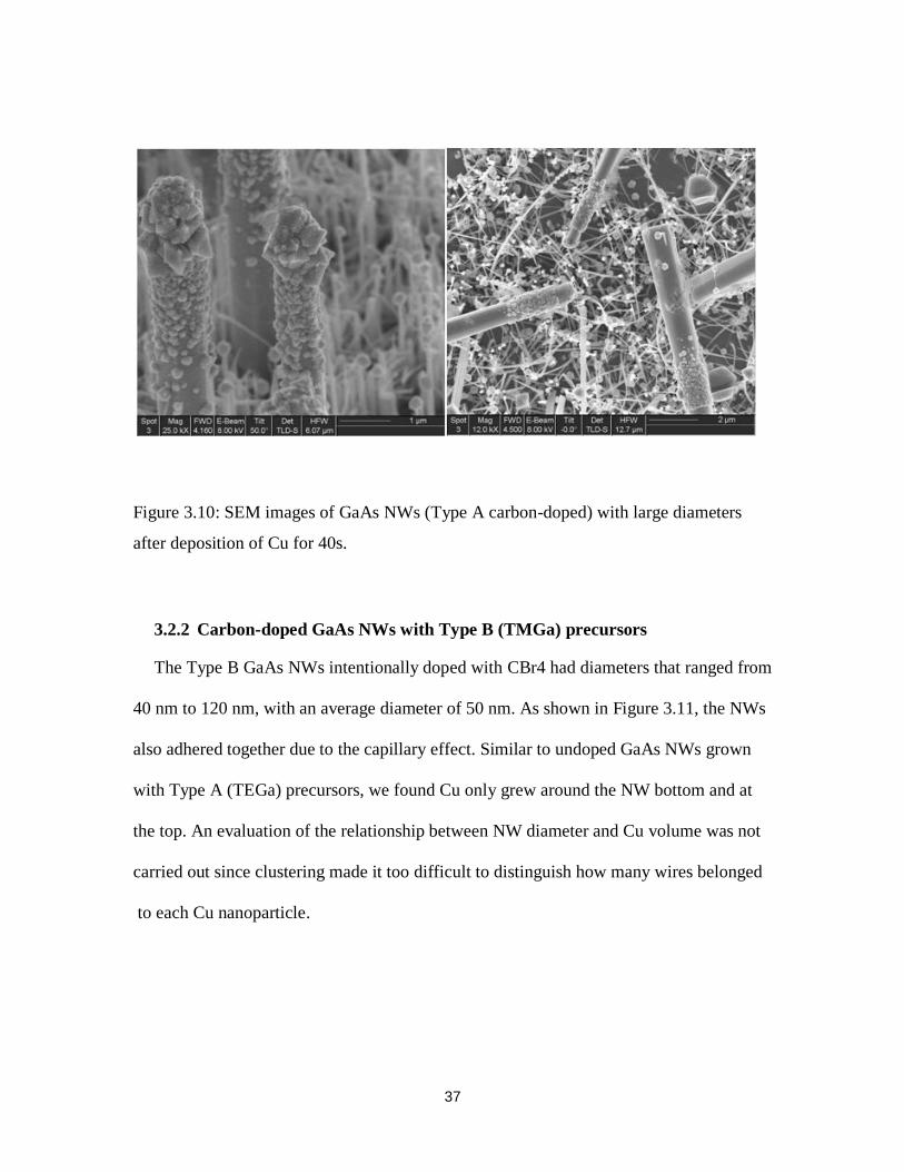
Figure 3.10: SEM images of GaAs NWs (Type A carbon-doped) with large diameters
after deposition of Cu for 40s............................................................................... 37

x
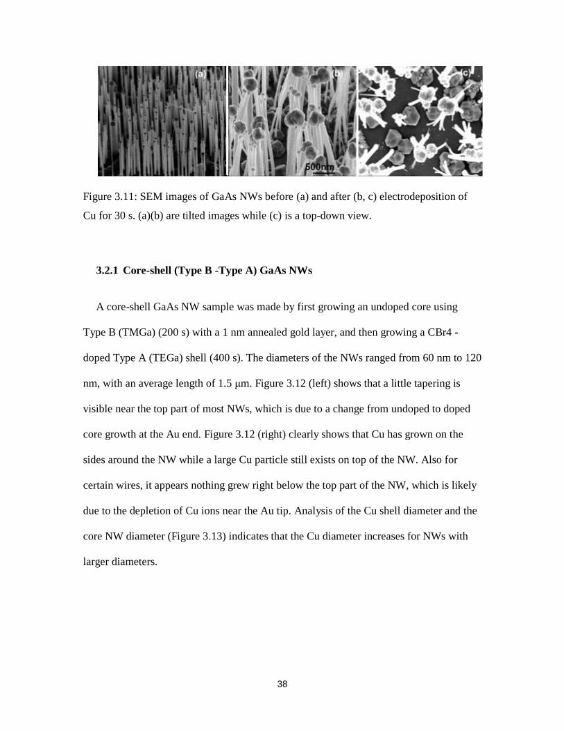
Figure 3.11: SEM images of GaAs NWs before (a) and after (b,c) electrodeposition of Cu
for 30 s. .............................................................................................................. 38
Figure 3.12: SEM images of undoped core, carbon-doped shell GaAs NWs before (left)
and after (right) electrodeposition of Cu for 40 s. .................................................. 39
Figure 3.13: Plot of Cu diameter on the sides of the NW vs. NW diameter. ............................. 39
Figure 3.14: SEM images of GaAs NWs before (left) and after (right) electrodeposition
of Fe for 30 s. ..................................................................................................... 40
Figure 3.15: Plot of calculated Fe nanoparticle volume as a function of NW diameter. ............. 41
Figure 3.16: TEM images of the GaAs NW after deposition of Fe for 30 s............................... 42
Figure 3.17: STEM image of a GaAs NW after deposition of Fe. ............................................ 43
Figure 3.18: A STEM image of the Au end of another wire electrodeposited with Fe and
EDS pattern. ....................................................................................................... 44
Figure 3.19: SEM images of InAs NWs from NRC obtained from two regions of the
same SiO2/InP patterned wafer ............................................................................ 45
Figure 3.20: SEM image of one InAs NW growing through a SiO2 masked InP substrate.. ....... 46
Figure 3.21: SEM images of InAs NWs with different array sizes after electrodeposition
of Cu for 30 s...................................................................................................... 47
Figure 3.22: Left: SEM image of one of the InAs NW after deposition of Cu. Right: EDS
spectrum of the red area shown in (a). .................................................................. 47
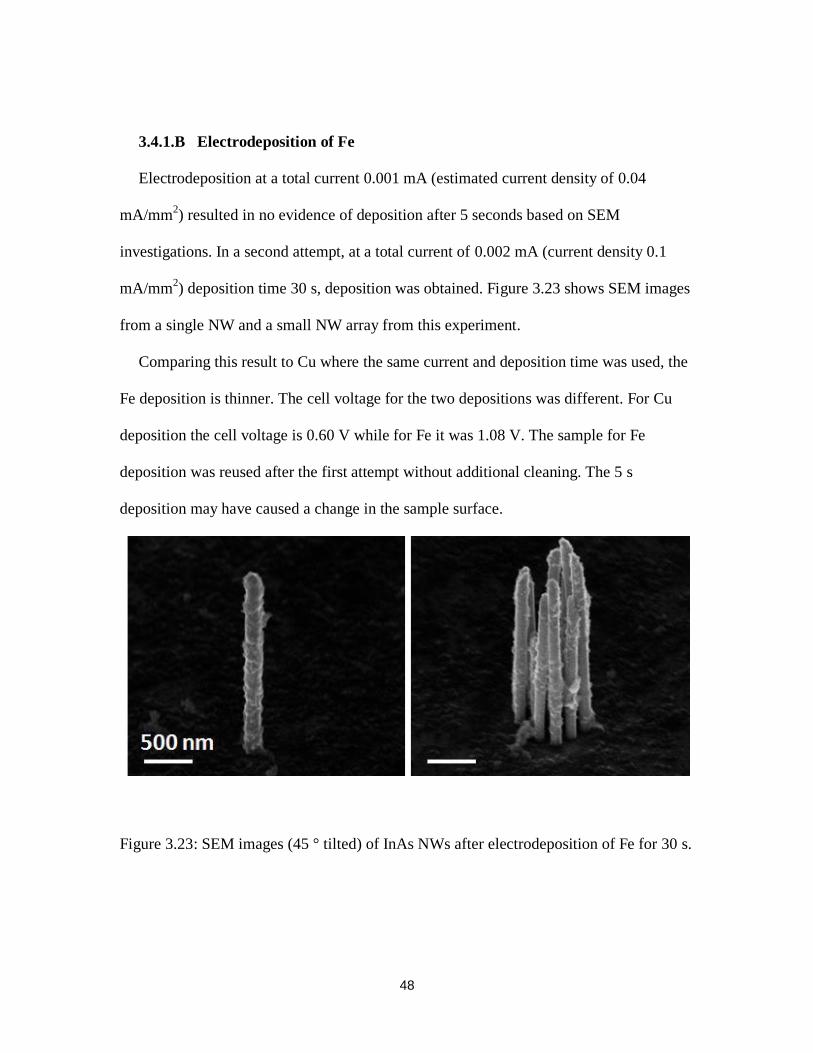
Figure 3.23: SEM images (45 ° tilted) of InAs NWs after electrodeposition of Fe for 30 s. ....... 48
Figure 3.24: SEM images of InAs NWs before (a) and after (b) electrodeposition of Cu
for 40 s. .............................................................................................................. 49
Figure 3.25: SEM images of GaAs NWs after electrodeposition of Cu for 30 s. ....................... 50
Figure 3.26: SEM images of Cu deposition on a gold nanoparticle/GaAs substrate sample
as a function of deposition time. .......................................................................... 51
Figure 3.27: SEM images of carbon-doped GaAs NWs (Type A) after 40 s
electrodeposition of Cu. ...................................................................................... 53
Figure 3.28: TEM images of GaAs NWs where the Au was etched prior to
electrodeposition of Cu (40 s). ............................................................................. 54
Figure 3.29: TEM bright field image of a ZB GaAs NW with associated SAD pattern.. ............ 55
Figure 3.30: Potential change as a function of deposition time. ............................................... 86
Figure 4.1: (a) NW current and calculated resistivity versus NW diameter and (b) current
versus NW cross-sectional area for Cu deposition. ................................................ 58
Figure 4.2: Calculated current versus NW diameter (a) and NW cross-sectional area (b)
for Fe deposition . ............................................................................................... 61
Figure 4.3: Sketch of the simulation deposition cell. .............................................................. 63
Figure 4.4: Copper ion concentration (mol/m3), isopotential lines (black), total flux
stream lines (white), and electrode displacement in the cell after 1 second of
operation. . ........................................................................................................ 66
xi
Figure 4.5: Copper ion concentration (mol/m3), isopotential lines, total flux stream lines,
and electrode displacement in the cell after (a) 2 s, (b) 3 s, (c) 4 s and (d) 5 s
of operation. ....................................................................................................... 67
Figure 4.6: GaAs NW sample sketch and lightning rod picture. .............................................. 68
Figure 4.7: Geometry of the electrolytic cell. ......................................................................... 69
Figure 4.8: Simulation results of (a) current density (A/m2) and (b) electric field (V/m)
distribution ......................................................................................................... 71
Figure 4.9: Simulation results of (a) current density (A/m2) and (b) electric field (V/m)
distribution in the cell for GaAs NWs with conductivity 106 S/m. ........................... 72
Figure 4.10: SEM image of GaAs NWs after Cu deposition for 5 s with 40 mA/mm2 ............... 75
Figure 4.11: SEM images of a nanoprobe touching electrodeposited Cu on a GaAs NW
head. .................................................................................................................. 78
Figure 5.1: Sketch of low-doped NW sample before and after electrodeposition. ..................... 79
Figure 5.2: Sketch of highly-doped NW sample before and after electrodeposition................... 80

xii
LIST OF TABLES
Table 2.1: Summary of NW samples deposited in this work. .................................................. 16
Table 2.2 The liquid-vapour interfacial energy density (surface tension) for water-air,
ethanol-air and 9.6% Aqueous ammonia (ammonium hydroxide) – air
interfaces at room temperature. [15] ....................................................................... 21

1
INTRODUCTION
Semiconductor nanowires have attracted wide attention as building blocks for the
next generation of nanoelectronic components or solar cells. While significant work had
been done on the bottom up fabrication of these one-dimensional nanostructures, direct
assembling or incorporating nanowires into nanosystems is important both for
characterization and for creating new functionality.
Various methods have been developed to assemble metal contacts onto
semiconductor NWs. There are two different kinds: end bonded or side contacts. A
common method for both types is to disperse the NWs onto an insulating substrate with
pre-patterned alignment markers and then fabricate the contacts through electron beam
lithography and metal evaporation [1][2][3]. Such contacts have also been achieved by
electrodeposition onto NWs dispersed onto pre-patterned metal electrodes [4] or directly
on the ends or sidewalls with the NWs still attached to the growth substrate [5].
In this work we studied the assembly of copper (Cu) and iron (Fe) contacts on
as-grown, GaAs and InAs vertical NWs using electrodeposition. During deposition, the
whole NW is surrounded by electrolyte, which makes both end and side contacts possible
under certain conditions. The experimental methods and some previous experimental
results on electrodeposition of metal on GaAs bulk sample will be reviewed briefly in
Chapter 1. Chapter 2 will discuss the electrodeposition experimental details, and sample
preparation including evaluating the wettability of NW surfaces. We will present the

2
experimental results in Chapter 3 and the analysis of the growth mechanisms in Chapter 4
in terms of NW conductivity, morphology and surface oxidation.

3
1: ELECTRODEPOSITION
1.1 Electrodeposition overview
Electrodeposition is the process of reducing metal ions into a solid by supplying
electrons to the electrode. A typical electrochemical cell consists of two electrodes
immersed in an electrolyte with a DC power supply connected to both electrodes. A
schematic of the set-up for Cu deposition on our GaAs NW sample is shown in Figure
1.1 where the electrolyte consists of copper sulphate (CuSO4) dissolved in de-ionized
water.
Figure 1.1: Schematic diagram of an electrodeposition cell. Galvanostatic
electrodeposition uses a constant current source with two electrodes: cathode and anode.

4
At the cathode (GaAs NW sample), positively charged ions (H+ and Cu
2+) are
attracted to the sample surface, reduced, and bonded to form a solid on the electrode (Cu)
or evolve as gas (H2). While at the anode (platinum), negatively charged ions (SO42-
and
OH-) are attracted and become oxidized. The major reactions can be written as:
Cathode: Cu2+
+ 2e- Cu (1.1)
Anode: 4OH- - 4e
- O2 + 2H2O (1.2)
In our experiment, we used a constant current power source (galvanostatic
electrodeposition). Many researchers use a constant voltage power source (potentiostatic
electrodeposition), where an extra reference electrode is used to control the cathode
voltage. That works best when the cathode is a good conductor with a reproducible, low
resistance contact. In our case, variations in both the bulk resistivity of the GaAs cathode
and the resistance of its ohmic contact meant that the control of current maintained a
constant voltage drop and flux of ions within the electrolyte.
1.1.1 Nernst’s equation and overpotential
Based on the principle of microscopic reversibility in electrochemistry, there is a
reverse reaction occurring during Cu deposition:
Cu Cu2+
+ 2e-
(1.3)
The Nernst equation gives the cathode potential required at equilibrium, Eeq,, i.e. when
no net current is flowing across the electrode/electrolyte interface [6]:
, (1.4)
where R is the universal gas constant, T is the absolute temperature, F is the Faraday
constant, z is number of electrons for the exchange reactions, which is 2 for Cu

5
deposition, and a is the chemical activity, which equals the molar concentration of
electron or acceptor ion in a dilute solutions. E0 is the standard hydrogen potential, given
the hydrogen chemical activity, aH+= 1. For copper sulphate with a 0.1 mol/L
concentration, we know the standard potential for Cu2+
Cu is 0.337 V [7], thus:
(1.5)
When the electrodes are connected to an electric power source that provides excess
charge, the equilibrium will be broken. The departure of the electrode potential from its
equilibrium value is called the overpotential.
η = E – Eeq (1.6)
1.1.2 Butler-Volmer equation
The Butler–Volmer equation is one of the most fundamental equations
in electrochemistry describing the relationship between current density and electrode
potential, considering that both a cathodic and an anodic reaction occur on the same
electrode [6]:
(1.7)
I is electrode current, i0 is exchange current density, n is number of electrons involved in
the electrode reaction, A is electrode active surface area, and is charge transfer
coefficient. The Butler-Volmer equation developed in the 1960’s is based on pure metal
electrodes. The process becomes more complicated when you have both metal and
semiconductor electrodes in the electrodeposition system explained further in the next
section.
6
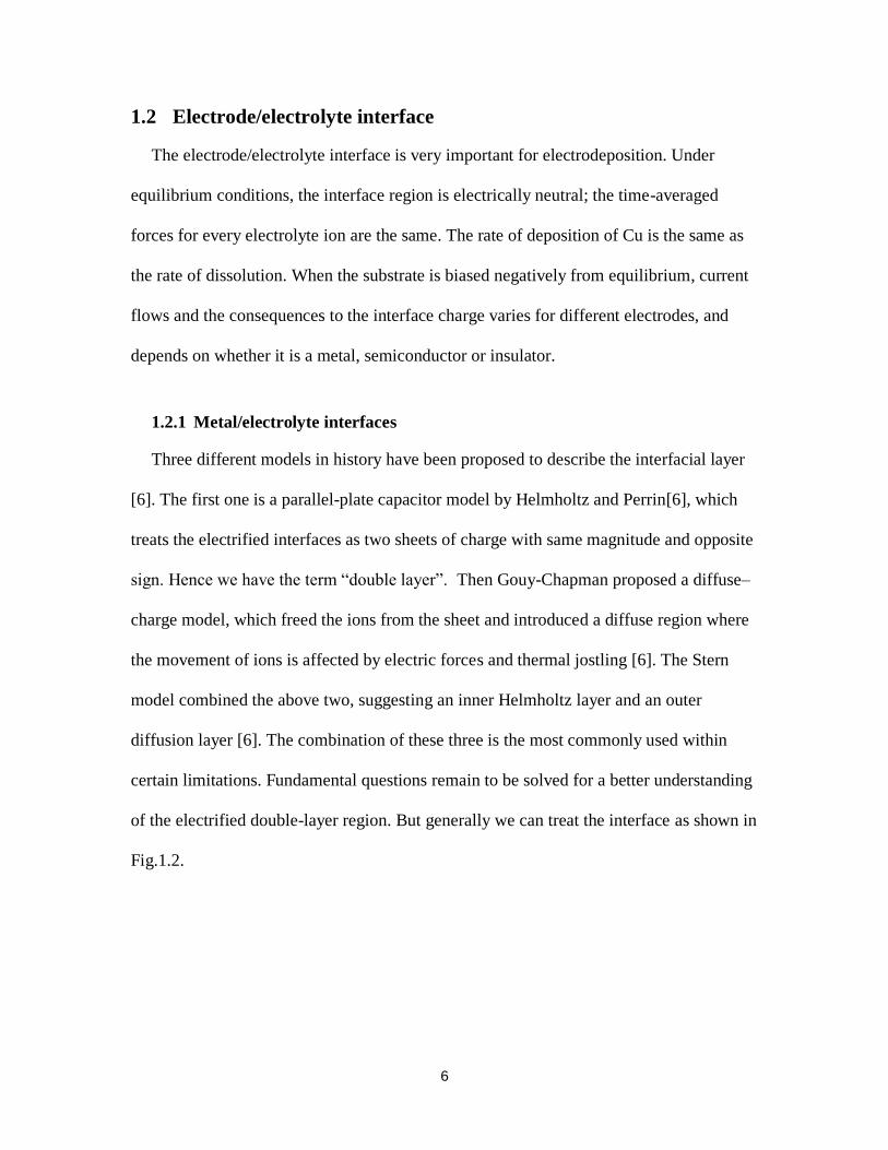
1.2 Electrode/electrolyte interface
The electrode/electrolyte interface is very important for electrodeposition. Under
equilibrium conditions, the interface region is electrically neutral; the time-averaged
forces for every electrolyte ion are the same. The rate of deposition of Cu is the same as
the rate of dissolution. When the substrate is biased negatively from equilibrium, current
flows and the consequences to the interface charge varies for different electrodes, and
depends on whether it is a metal, semiconductor or insulator.
1.2.1 Metal/electrolyte interfaces
Three different models in history have been proposed to describe the interfacial layer
[6]. The first one is a parallel-plate capacitor model by Helmholtz and Perrin[6], which
treats the electrified interfaces as two sheets of charge with same magnitude and opposite
sign. Hence we have the term “double layer”. Then Gouy-Chapman proposed a diffuse–
charge model, which freed the ions from the sheet and introduced a diffuse region where
the movement of ions is affected by electric forces and thermal jostling [6]. The Stern
model combined the above two, suggesting an inner Helmholtz layer and an outer
diffusion layer [6]. The combination of these three is the most commonly used within
certain limitations. Fundamental questions remain to be solved for a better understanding
of the electrified double-layer region. But generally we can treat the interface as shown in
Fig.1.2.

7
Figure 1.2: Schematic diagram of a doublelayer on an electrode: 1. Inner Helmholtz
layer, largely occupied by water dipoles and a very few unsolvated negative ions, which
can be considered as a hydration sheath of the electrode. 2. Outer Helmholtz layer,
largely distributed solvated positive ions. 3. Electrolyte diffusion layer. 4. Solvated ions.
5. Adsorbed foreign ion. 6. Water molecules [8].
The Helmholtz layer (inner and outer) is 1.5 to 2.0 times the thickness of a mono-
molecular water layer, smaller than 1 nm. Similar to the diffusion layer in the electrolyte,
interfacial excess charge on the metal electrode is distributed from the solid face towards
the interior forming a diffuse layer of excess electrons. This diffusive layer is called the
“surface charge layer”. The thickness of the diffusion and space charge layers depend on
the concentration of mobile charge carriers, characterized by the Debye length, Ld.
8
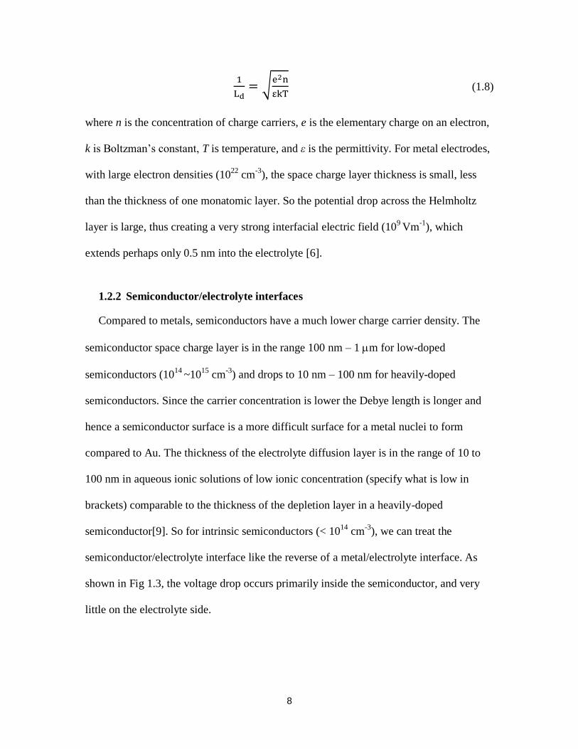
(1.8)
where n is the concentration of charge carriers, e is the elementary charge on an electron,
k is Boltzman’s constant, T is temperature, and ε is the permittivity. For metal electrodes,
with large electron densities (1022
cm-3
), the space charge layer thickness is small, less
than the thickness of one monatomic layer. So the potential drop across the Helmholtz
layer is large, thus creating a very strong interfacial electric field (109 Vm
-1), which
extends perhaps only 0.5 nm into the electrolyte [6].
1.2.2 Semiconductor/electrolyte interfaces
Compared to metals, semiconductors have a much lower charge carrier density. The
semiconductor space charge layer is in the range 100 nm – 1 m for low-doped
semiconductors (1014
~1015
cm-3
) and drops to 10 nm – 100 nm for heavily-doped
semiconductors. Since the carrier concentration is lower the Debye length is longer and
hence a semiconductor surface is a more difficult surface for a metal nuclei to form
compared to Au. The thickness of the electrolyte diffusion layer is in the range of 10 to
100 nm in aqueous ionic solutions of low ionic concentration (specify what is low in
brackets) comparable to the thickness of the depletion layer in a heavily-doped
semiconductor[9]. So for intrinsic semiconductors (< 1014
cm-3
), we can treat the
semiconductor/electrolyte interface like the reverse of a metal/electrolyte interface. As
shown in Fig 1.3, the voltage drop occurs primarily inside the semiconductor, and very
little on the electrolyte side.

9
Figure 1.3: Potential drop at the semiconductor-electrolyte interface (schematic) [9].
1.3 Previous work on electrodeposited epitaxial metal on GaAs
Previous work by Dr. Zhiliang Bao showed that epitaxial Cu can be
electrodeposited onto single crystalline GaAs substrate. The optimal growth condition
determined was 53 °C with a current density 0.1 mA/mm2 from pure CuSO4 (0.1 M) [10].
Figure 1.4 shows an x-ray diffraction θ-2θ scan of Cu/GaAs (001) and a SEM image of
the sample surface. We can see that the Cu film surface shows well-aligned pyramidal
shapes.
Dr. Bao also summarised three key process parameters that are essential to achieve
epitaxial Fe deposition on GaAs substrate. One is the addition of ammonium sulphate to
the electrolyte: optimum epitaxy occurs for (NH4)2SO4/FeSO4 ratios of 1:3. The second
is setting the deposition current density to 0.1 mA/mm2. The third is using ammonium
hydroxide to etch the GaAs native oxide before electrodeposition [11].

10
Figure 1.4: (a) XRD θ-2θ scans of Cu/GaAs deposited at 53°C onto (001) oriented
substrate and (b) SEM image of the sample surface [10].
1.4 Electrodeposition setup
Figure 1.5 shows photographs of the electrodeposition system. It consisted of a
glass beaker (Kimax 20 ml) on a support stand with anode and cathode suspended, and a
computer-controlled power supply (Keithley 2400). The power supply provided a
constant current from 10 pA to 1 A within a voltage compliance range ±100 V. A
labview program was used to control the current output and record the voltage and
current data. We used platinum wire as the anode. Ohmic contact between the GaAs
substrate and the experimental apparatus was made via InGa liquid alloy on the backside
of the sample (not the nanowire side). The nanowire side faced the platinum wire inside
the cell. Stainless steel tweezers (Almedic #3 Switzerland) with a sharp and tight tip were

11
used to hold the sample. Photoresist, as an inert insulator, was used to define the
Figure 1.5: Schematic diagram of the circuit with a photo of the deposition cell.
growth window for the sample. As shown in Figure 1.6, photoresist was painted on the
backside as well as on the edges of the GaAs NW sample.
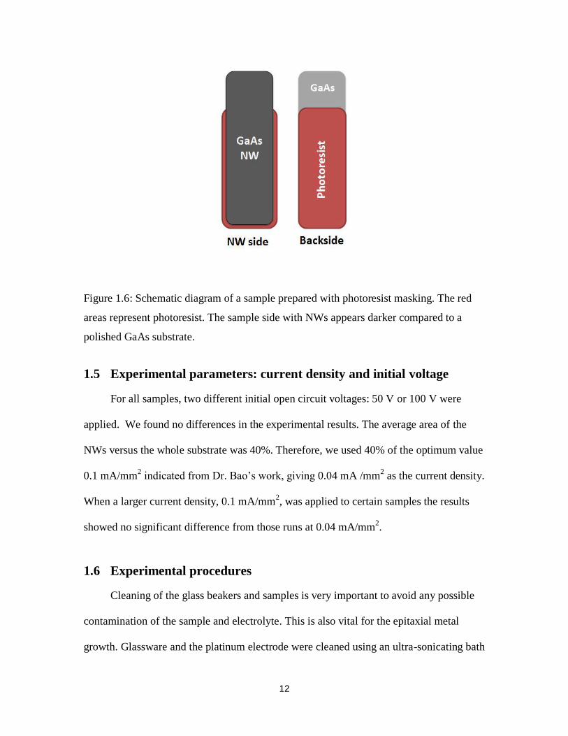
12
Figure 1.6: Schematic diagram of a sample prepared with photoresist masking. The red
areas represent photoresist. The sample side with NWs appears darker compared to a
polished GaAs substrate.
1.5 Experimental parameters: current density and initial voltage
For all samples, two different initial open circuit voltages: 50 V or 100 V were
applied. We found no differences in the experimental results. The average area of the
NWs versus the whole substrate was 40%. Therefore, we used 40% of the optimum value
0.1 mA/mm2 indicated from Dr. Bao’s work, giving 0.04 mA /mm
2 as the current density.
When a larger current density, 0.1 mA/mm2, was applied to certain samples the results
showed no significant difference from those runs at 0.04 mA/mm2.
1.6 Experimental procedures
Cleaning of the glass beakers and samples is very important to avoid any possible
contamination of the sample and electrolyte. This is also vital for the epitaxial metal
growth. Glassware and the platinum electrode were cleaned using an ultra-sonicating bath
13
in isopropanol then doubly-deionized water (DDI), each for 5 minutes. This process
removes any micro-dust or other particulate matter that may interfere with the metal
deposition.
Samples were prepared by cleaving the as-received GaAs NW sample into 15-30
mm2 pieces. The backside and the edges of the sample piece were then coated with
photoresist. After sufficient drying of the photoresist paint at room temperature (10
hours), the deposition area was measured for calculation of current.
The oxide etching solution consisted of ammonium hydroxide (10%) made by
diluting 28% ammonium hydroxide with doubly deionized (DDI) water. The electrolytes
consisted of 0.1 M CuSO4 using DDI water for Cu or 0.1 M FeSO4 with 0.3 M
(NH4)2SO4 for Fe.
Ohmic contact was made to the substrate backside; the area was first etched with
10% ammonium hydroxide and then dried. A large area of InGa was scratched onto the
surface and stainless tweezers were securely attached to the substrate.
The dried platinum wire and tweezers with sample attached were assembled onto
the experiment stand. The sample was first etched for 10 seconds in 10% ammonium
hydroxide to remove the native oxide then immersed in DDI water for another 10
seconds. The power supply was turned on and then the sample under open-circuit voltage
was immersed in the electrolyte for metal deposition. The deposition time (20 – 60 s) was
controlled by a labview program; the power was turned off when the deposition process
reached the preset time.
After deposition, the sample was rinsed in acetone to remove the photoresist and
then cleaned with isopropanol and deionized water. The InGa contact could be removed
14
by ammonium hydroxide using a cotton swab. The beakers and platinum wire were
immersed in concentrated sulphuric acid and then rinsed by deionized water. The beakers
and platinum wire were stored when not in use immersed in 2-propanol inside a sealed
large beaker, to prevent contamination.
After our sample was totally dried, the deposited structure was studied using
scanning electron microscopy (FEI Strata Dual Beam 235 Scanning Electron
Microscope) (SEM) operating at 5 keV. The NWs were mechanically transferred to a
carbon-coated grid for TEM analysis using a FEI Tecnai 20 field emission Scanning
Transmission Electron Microscope (STEM) operating at 200 keV.
15
2: NANOWIRE SAMPLES
2.1 NW samples
GaAs and InAs NWs from Dr. Simon Watkins’ group (Simon Fraser University)
and InAs NWs from Dr. Philip Poole (Institute for Microstructural Sciences, NRC
Canada) were used for the deposition experiments. All wires were (111) oriented and
grown on (111)B oriented single crystalline substrates. Table 2.1 lists the details of the
NW samples used for this work. GaAs nanowires were grown epitaxially on n-type Si-
doped GaAs substrates by gold-catalyzed vapour liquid solid (VLS) growth in a
metalorganic vapour phase epitaxy (MOVPE) reactor. To control conductivity, growth
with a carbon dopant source were investigated. The carbon concentration was controlled
with the addition of carbon tetrabromide gas (CBr4) during growth. The As precursor was
tertiarybutylarsine (TBAs) while there were two different types of Ga precursors, Type
A: triethylgallium (TEGa) and Type B: trimethylgallium (TMGa) [12][13].
Unintentional carbon doping of GaAs NWs can occur via the Ga precursor used in
the MOCVD growth as a function of temperature, as well as from intentional carbon
doping when CBr4 was added. Nevertheless, for convenience, “doped or undoped NWs”
refers to GaAs NWs grown using either TEGa or TMGa with TBAs precursors and with
or without CBr4, respectively. “Core-shell NWs” refers to wires grown with an undoped
GaAs core, followed by a doped GaAs shell.
InAs NWs obtained from Dr. Watkin’s group were grown at a temperature of 440
°C using trimethylindium (TMIn) as the group III precursor and TBAs as the group V
16
precursor. The NWs were unintentionally doped and the substrate was n-type GaAs
doped with Si (~ 5x10¹⁷
/cm3).
InAs NWs from NRC were grown epitaxially on n-type InP substrates without
gold catalyst. These wires were grown from small patterned openings (~160 nm) in a 20
nm thick SiO2 layer that covered the entire top surface of the InP wafer.
Table 2.1: Summary of NW samples deposited in this work.
NW MOCVD
Run No.
Ga or In
Precursor
Doping Metal
Deposited
Time
(s)
Location Section
GaAs 5849 TEGa CBr4 Cu 40 Au 3.2.1
5902 undoped Cu 40 Au 3.1.1
5906
coreshell
2/3 CBr4
1/3undoped
Fe 30 Au 3.3
6027 TMGa CBr4 Cu 30 Au 3.2.2
6026 undoped Cu 30 Au 3.1.2
6059 Core TMGa
Shell TEGa
undoped
CBr4
Cu 40 Au and
sidewall
3.2.3
InAs 6060 TMIn undoped Cu 40 Au and
sidewall
3.4.2
NRC TMIn undoped Cu, Fe 30 Top and
sidewall
3.4.1

17
2.2 Wettability of sample surfaces
We investigated the effects of sample preparation on water repellancy as measured
by the contact angle of liquid drops on each surface. Although the NW substrates are
totally immersed in the electrolyte during the deposition this does not necessarily mean
that the entire NW was in contact with the electrolyte.
Young’s Equation describes the contact angle Θc of a liquid droplet on a flat, solid
surface as a function of interfacial surface tensions (Figure 2.1):
cos Θc = (γSV- γSL)/γLV , (2.1)
where γSV, γSL, and γLV are the solid-vapour, solid-liquid, and liquid-vapour interfacial
surface tensions, respectively, in units of force per unit length. A lower γLV or γSL will
cause a smaller contact angle. Sample surfaces were examined using a contact angle
instrument consisting of an optical microscope and built-in software for angle
measurement (VCA Optima located in Dr. Hogan Yu’s Lab in 4D Labs) [14].
Figure 2.1: Illustration of the contact angle, c, of a liquid droplet on a substrate as a
function of the interfacial surface tensions, solid liquid (SV), solid vapour (SV) and
liquid vapour (LV).

18
2.2.1 As-received sample surfaces
Figure 2.2 shows different as-received sample surfaces under SEM and the
corresponding de-ionized water droplet on the surface under an optical microscope. The
measurement of contact angle was obtained from the optical images of the liquid drop
interfaces for each sample surface. The red lines on each image are tangents to the drop
and substrate surfaces at their intersection.
The pure as-received GaAs (111) B substrates were hydrophobic, with a contact angle
ranging from 65° to 70°. The evaporation of Au nanoparticles onto these GaAs substrates
made the surface more hydrophobic, with larger contact angles ranging from 85° to 100°.
Even larger contact angles, greater than 150°, were found for some of the NW samples,
e.g. (c) and (d) while others (e) and (f) had contact angles of zero becoming hydrophilic.
The wetting properties of GaAs NWs have been reported to be a function of surface
geometry, the length of the NWs [15], the wire density and the morphology of NWs [16].
It is found that hydrophobic behavior becomes more pronounced as the length of the
nanowires increases [15]. Figure 2.3 shows a series of contact angle measurements taken
for different as-received GaAs NW samples as a function of NW diameter, length, and
density and the gold thickness. Consistent with the literature reports, nanowire diameters
greater than 200 nm, or lengths greater than 2 μm, or density less than 15 m-2
, about half
of the samples are hydrophobic with average contact angles of 140. The NWs with
higher densities are mostly those that also had smaller diameters. These results indicate
that surface preparation to enhance wetting is required.
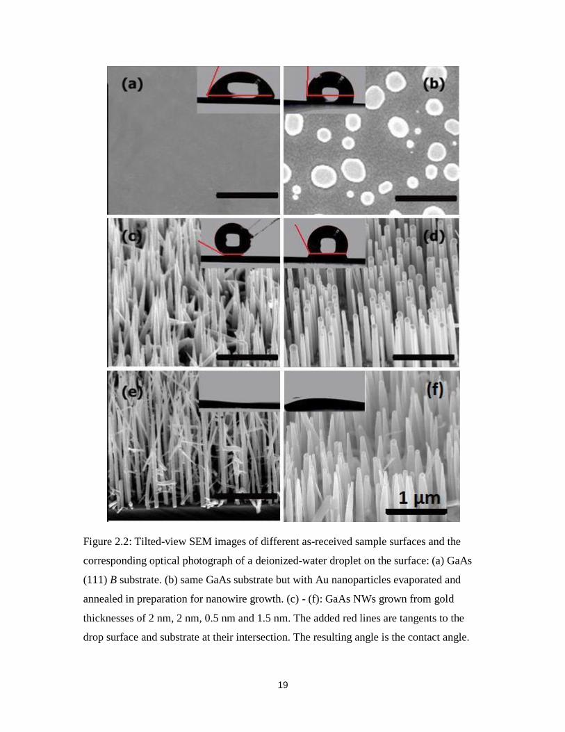
19
Figure 2.2: Tilted-view SEM images of different as-received sample surfaces and the
corresponding optical photograph of a deionized-water droplet on the surface: (a) GaAs
(111) B substrate. (b) same GaAs substrate but with Au nanoparticles evaporated and
annealed in preparation for nanowire growth. (c) - (f): GaAs NWs grown from gold
thicknesses of 2 nm, 2 nm, 0.5 nm and 1.5 nm. The added red lines are tangents to the
drop surface and substrate at their intersection. The resulting angle is the contact angle.

20
Figure 2.3. Plots of contact angle versus NW (a) diameter, (b) length, and (c) density and
(d) gold film thickness (before annealing to form gold nanoparticles for MOCVD NW
growth).
2.2.2 GaAs NW surfaces after ammonium hydroxide etching
It has been reported that alkaline treated GaAs bulk surfaces are hydrophilic [17],
attributed to the OH groups left on the GaAs surfaces. Our GaAs substrates and NW
samples when etched in (NH4)OH, also became hydrophilic with the solution completely
wetting the surface like those in Figure 2.2 (e) or (f). All samples also became
hydrophilic after immersion in ethanol, consistent with its lower surface tension

21
compared to water [18]. Table 2.2 compares surface tensions for air interfaces with water,
ethanol and ammonium hydroxide (9.6%). Ethanol has a much lower surface tension
compared to water, or ammonium hydroxide. Experiments with dipping the nanowires in
ethanol followed by rinsing in water prior to electrodeposition showed that ethanol
treated GaAs NW surfaces also became hydrophilic.
Interface with air γ (mN·m–1
)
Water 72.86
Ethanol 22.39
Ammonium Hydroxide (9.6%) 67.85
Table 2.2 The liquid-vapour interfacial surface tension for water-air, ethanol-air and
9.6% Aqueous ammonia (ammonium hydroxide) – air interfaces at room temperature. [19]
2.3 Removal of gold
To check the effect of the Au catalyst on NW electrodeposition a method to remove
the gold before deposition was needed. There are two commonly used wet etching
solutions that dissolve gold [20] including (1) mixtures of nitric acid (HNO3) and
hydrochloric acid (HCl) (ratio 1: 3) and (2) fresh aqueous solution of I2 and KI (aqueous
tri-iodide) (KI : I2 : H2O = 4 g : 1 g : 40 ml). Fresh solutions are necessary since the
iodine oxidizes easily in water. It is known that nitric acid will damage a GaAs surface
[21], therefore, we chose to use aqueous tri-iodide to remove the Au catalysts. Figure 2.4
(b) shows SEM images of GaAs substrates with gold nanoparticles only and nanowires

22
with Au catalysts after etching in tri-iodide. In both cases the Au particles are gone but
there is obvious damage to the nanowires. Similar damage was reported for Ge NWs
when etched in KI/I2. [22] They reduced this problem by adding HCl to the etching
solution, which protected the Ge NWs likely by a chlorine-based surface passivation.
Based on this work we carried out a second set of Au etching experiments adding HCl to
the tri-iodide etching solution (2 mL 35% HCl in 15 mL tri-iodide). Figure 2.4 (b left)
shows an SEM image of the same Au nanoparticle GaAs sample as in (a left) but after
such etching. We can see that there are round-shaped depressions left on the substrate,
which likely indicate the original location of gold nanoparticles that had reacted with the
substrate, or that the etch has caused new damage to the GaAs substrate. Similarly,
Figure 2.4 (c right) shows an SEM image of GaAs NWs that shows clearly that the gold
catalysts were removed with minimal damage to the GaAs NWs. (The size of the Au
nanoparticles on GaAs in this case were larger than those used to grow the NW samples
shown.)

23
Figure 2.4: SEM images left side: gold nanoparticles on GaAs (111) sample, right
side GaAs NWs: (a) as-deposited and (b) and (c) after gold etching in KI/I2
solutions:(b) without HCl, and (c) with HCl.

24
2.4 Light-assisted electrodeposition
Photocurrent can be generated from GaAs NWs under visible or ultraviolet (UV)
illumination [23]. Experimental results of photoconductivity measurements for GaN
nanowires also indicate that the generated current from the NW increased considerably
under UV illumination [24]. Light-assisted electrochemical deposition of metal films on
Si or GaAs substrates has been reported years ago [25][26]. The deposition rate increases
significantly for Au on p-Si under illumination (l00-W tungsten-halogen lamp) compared
to in the dark [25]. Also, there is intensive study about photo-electrochemical deposition
used to form patterned metal films [26]. Since our GaAs nanowires were potentially
carbon-doped, meaning p-type, it was interesting to check if light during
electrodeposition would have an effect on metal growth rates.
To investigate the effect of light exposure, electrodeposition experiments were
performed on GaAs substrates as a function of illumination from an LED white light
source. The band gap energy of intrinsic GaAs (1.42 eV at room temperature) is
equivalent to the energy of a photon with a wavelength of 870 nm (infrared). Since we
used a glass beaker (Kimax 20 mL No.14000) to hold the electrolyte and sample, it was
important to measure the transmission spectra of the light source through glass to predict
the intensity spectra that would expose our GaAs substrates.
Figure 2.5 shows transmission spectra measured using a spectrometer (spm-002
by Photon Control) with a spectral detection range from ultra violet (UV), (200 nm) to
near-infrared (1700 nm). The source generated light with two major peaks at 440 nm and
550 nm with absorption losses of 50% through the glass. The UV light from a lamp (peak
position 254 nm) was totally absorbed by the glass. For the electrodeposition experiment,
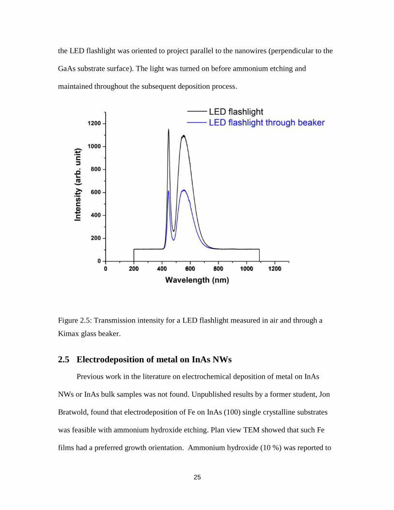
25
the LED flashlight was oriented to project parallel to the nanowires (perpendicular to the
GaAs substrate surface). The light was turned on before ammonium etching and
maintained throughout the subsequent deposition process.
Figure 2.5: Transmission intensity for a LED flashlight measured in air and through a
Kimax glass beaker.
2.5 Electrodeposition of metal on InAs NWs
Previous work in the literature on electrochemical deposition of metal on InAs
NWs or InAs bulk samples was not found. Unpublished results by a former student, Jon
Bratwold, found that electrodeposition of Fe on InAs (100) single crystalline substrates
was feasible with ammonium hydroxide etching. Plan view TEM showed that such Fe
films had a preferred growth orientation. Ammonium hydroxide (10 %) was reported to

26
be used for indium surface preparation prior to growing metal contacts on InAs bulk
samples using electron-beam evaporation [27]. Thus, we used the same surface
preparation that we used for GaAs NWs for the preparation of copper deposition on InAs
NWs. We also chose to use similar electrodeposition parameters, i.e. electrolyte
concentration: 0.1 mol/L CuSO4, current density: 0. 1 mA/mm2 and at room temperature.
27
3: RESULTS
This chapter is organized into six sections with SEM and TEM results from the
electrodeposition of two metals (Fe, Cu) onto two different semiconductor NWs (InAs
and GaAs).
3.1 Electrodeposition of Cu on GaAs NWs
3.1.1 Unintentionally-doped GaAs NWs - Type A Ga precursor (TEGa)
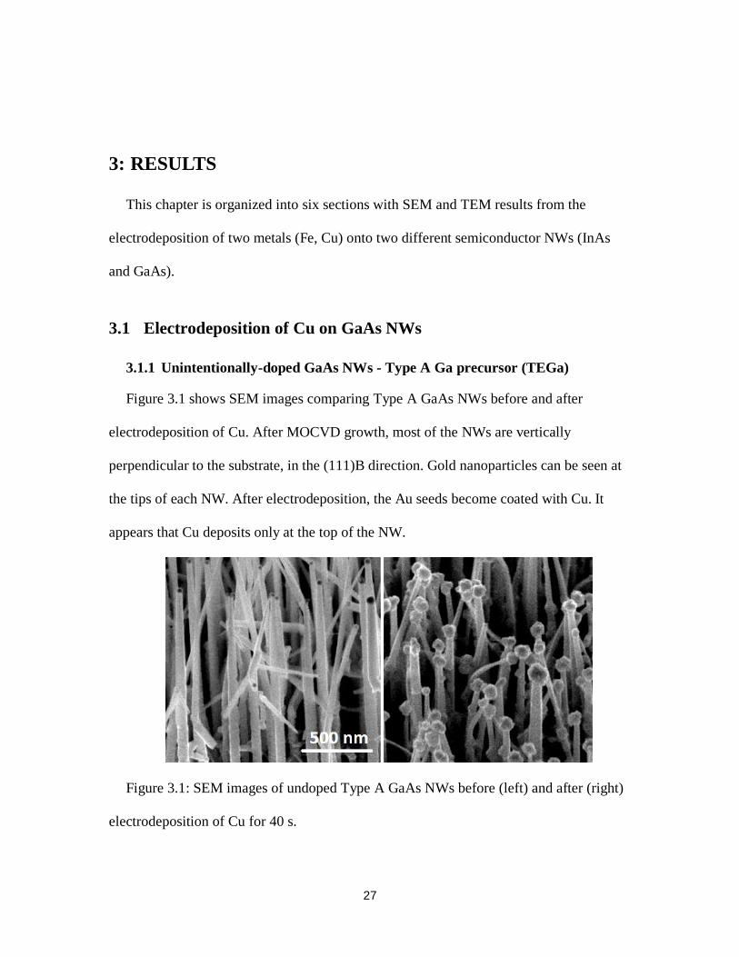
Figure 3.1 shows SEM images comparing Type A GaAs NWs before and after
electrodeposition of Cu. After MOCVD growth, most of the NWs are vertically
perpendicular to the substrate, in the (111)B direction. Gold nanoparticles can be seen at
the tips of each NW. After electrodeposition, the Au seeds become coated with Cu. It
appears that Cu deposits only at the top of the NW.
Figure 3.1: SEM images of undoped Type A GaAs NWs before (left) and after (right)
electrodeposition of Cu for 40 s.

28
TEM images shown in Figure 3.2 of these wires give a higher magnification-view of
their crystal structure. The first image is a low magnification image of the entire wire
after removal from the substrate onto the grid. The image at the bottom right is the
enlarged view of the top part of the NW. We can see that the Cu/Au particle looks darker
due to its greater thickness compared to the GaAs. The large period fringes visible are
most likely due to translational Moiré fringes from overlapping Au-Cu regions with
different lattice constants. The spacing between the Moiré fringes (1.6 0.3 nm),
compares to the calculated spacing of translational Moiré fringes from Au-Cu (111) (1.81
nm) [28]. From the BF images (a) and (c) we can see that the Cu crystal has hexagonal
facets, which indicates a single crystalline epitaxial material. The selected area diffraction
pattern in (b) shows that the GaAs wire is (110) oriented in the plane of the image with a
growth direction of [111] as expected. The Cu and Au diffraction spots are not clearly
visible from this wire.

29
Figure 3.2: TEM bright field images of a undoped Type A GaAs NW: (a)(c), and the
SAD pattern from the Au end region, (b) after electrodeposition of Cu for 40
s. Image (c) shows the enlarged version of the top part of the NW (a). In
graph (b) the circled indexed points are diffraction spots from GaAs. The
solid line circles are calculated diffraction rings for polycrystalline Au and
the dashed line circles are calculated diffraction rings for polycrystalline Cu.
3.1.2 Unintentionally-doped GaAs NWs: Type B Ga precursor (TMGa)
The difference between NW growth using TMGa and TEGa precursors is fully discussed
in references [12] [13]. Briefly, tapering has been found for Type A GaAs NWs (TEGa)
while Type B (TMGa) NWs exhibit much higher axial growth rates, as well as a dramatic
reduction in tapering. It was also found that growth with CBr4 is associated with less
30
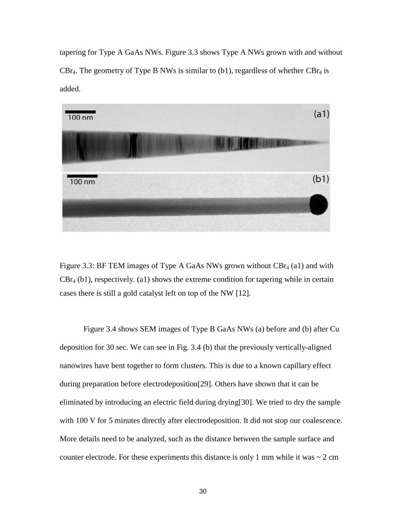
tapering for Type A GaAs NWs. Figure 3.3 shows Type A NWs grown with and without
CBr4. The geometry of Type B NWs is similar to (b1), regardless of whether CBr4 is
added.
Figure 3.3: BF TEM images of Type A GaAs NWs grown without CBr4 (a1) and with
CBr4 (b1), respectively. (a1) shows the extreme condition for tapering while in certain
cases there is still a gold catalyst left on top of the NW [12].
Figure 3.4 shows SEM images of Type B GaAs NWs (a) before and (b) after Cu
deposition for 30 sec. We can see in Fig. 3.4 (b) that the previously vertically-aligned
nanowires have bent together to form clusters. This is due to a known capillary effect
during preparation before electrodeposition[29]. Others have shown that it can be
eliminated by introducing an electric field during drying[30]. We tried to dry the sample
with 100 V for 5 minutes directly after electrodeposition. It did not stop our coalescence.
More details need to be analyzed, such as the distance between the sample surface and
counter electrode. For these experiments this distance is only 1 mm while it was ~ 2 cm

31
in our case. The diameters of these NWs ranged from 60 to 120 nm, averaging 70 nm.
Combining a top view with tilted images, the Cu crystals are distinguished from the
substrate surface or nanowires as isolated faceted particles are found around the bottom
of the NWs, as well as at the top. The diameter of the Cu on top of the NWs is not
uniform, which is possibly due to the cluster structure.
Figure 3.4: SEM images of type B GaAs NWs before (a) and after (b, c) Cu
electrodeposition for 30 s. (b) is a top view while (a) and (c) are tilted images (45°). The
arrows point to examples of Cu crystals.
3.2 GaAs NWs intentionally doped with carbon
Three different kinds of GaAs NWs intentionally doped with carbon using CBr4 were
examined for deposition. The first two varied the type of Ga precursor, Type A or Type
B. The third samples were core-shell with a Type A core and a Type B shell. The effects
of these growth conditions on the effectiveness of carbon doping was unknown. The
intention was to investigate variations in the conductivity in the NWs by monitoring the
rate of metal electrodeposition.

32
3.2.1 Type A TEGa precursor
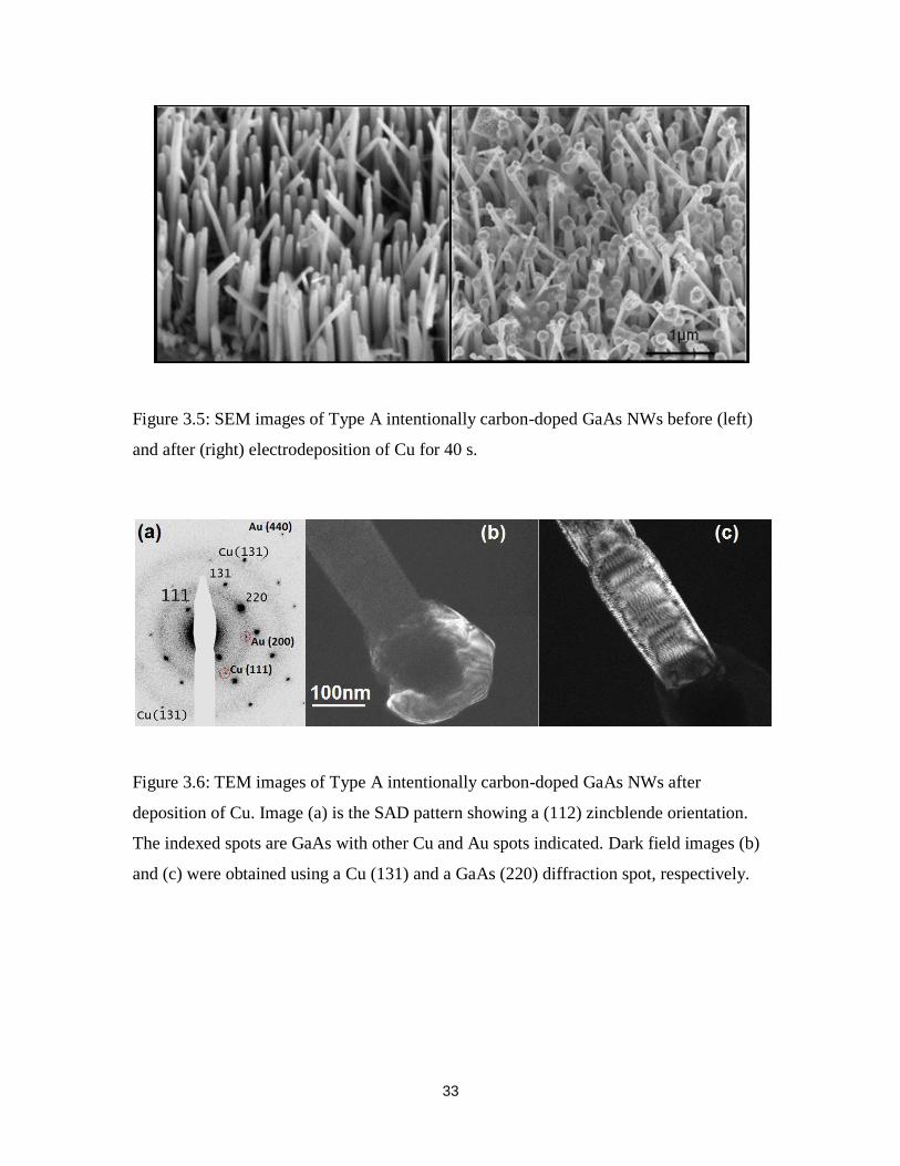
Figure 3.5 shows SEM images of intentionally carbon-doped Type A GaAs NWs
before and after Cu electrodeposition. Cu is predominantly found on the top of the NWs
or as isolated large crystals on the substrate. As seen in the TEM images of Figure 3.6 (c),
these GaAs NW grew along the (111) direction and thickness fringes appear around the
NW centre and edge. The diffraction pattern indicates that the electron beam was
perpendicular to a GaAs (112) plane, with the Cu (111) planes almost parallel to the the
GaAs (111) planes. Gold (111) also aligns with the GaAs (111) planes, in an epitaxial
arrangement [31].
Dark field TEM images of one of these wires are shown in Figure 3.6 (b). They
indicate that the Cu at the top of GaAs is a single crystal of orientation [112] the same as
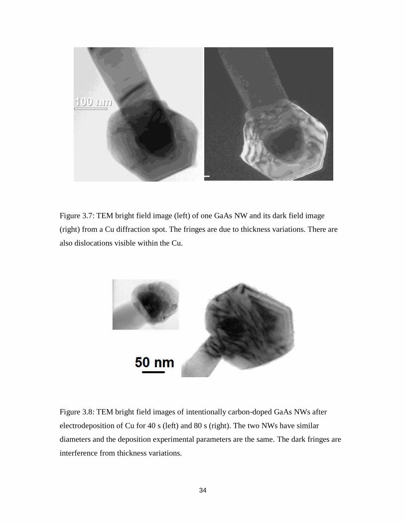
the GaAs crystal and Au. Figure 3.7 shows TEM bright field and dark field images of
another GaAs NW with the same orientation. We can see that the Cu crystal is a perfect
hexagonal shape, surrounding the Au catalyst (the darker part) inside. The dark field
image confirms that we have single crystalline copper growing on top of single
crystalline GaAs.
Figure 3.8 illustrates the increase of the Cu crystal volume on top of two different
intentionally carbon-doped Type A GaAs NW with double the deposition time, (from 40
s to 80 s) under otherwise similar experimental conditions. Longer deposition times gave
larger Cu particles.
33
Figure 3.5: SEM images of Type A intentionally carbon-doped GaAs NWs before (left)
and after (right) electrodeposition of Cu for 40 s.
Figure 3.6: TEM images of Type A intentionally carbon-doped GaAs NWs after
deposition of Cu. Image (a) is the SAD pattern showing a (112) zincblende orientation.
The indexed spots are GaAs with other Cu and Au spots indicated. Dark field images (b)
and (c) were obtained using a Cu (131) and a GaAs (220) diffraction spot, respectively.
34
Figure 3.7: TEM bright field image (left) of one GaAs NW and its dark field image
(right) from a Cu diffraction spot. The fringes are due to thickness variations. There are
also dislocations visible within the Cu.
Figure 3.8: TEM bright field images of intentionally carbon-doped GaAs NWs after
electrodeposition of Cu for 40 s (left) and 80 s (right). The two NWs have similar
diameters and the deposition experimental parameters are the same. The dark fringes are
interference from thickness variations.

35
3.2.1.B Nanowire diameter and geometry
Due to the distribution of diameters of the Type A GaAs NWs, we are able to analyse
the relationship between NW diameter and the volume of deposited Cu. Figure 3.9 shows
the experimental results for one GaAs sample with NW diameters ranging from 50 nm to
140 nm. Calculation of the Cu volume is based on the assumption that the Cu
nanoparticle is a sphere. Some data points have larger error bars because the Cu crystals
actually are facetted with different radii at different orientations. We corrected the Cu
volume by deducting the volume of the inside gold hemisphere and GaAs core. The
linear fit intersects the x-axis at 50 nm, suggesting that there may not have been copper
growing on GaAs NWs with diameters less than 50 nm.
We also found Cu nanoparticles growing around the nanowire shaft as well as at the
top for larger diameter (~ 1 μm) NWs. Figure 3.10 shows SEM images from Type A C-
doped GaAs NWs. The gold nanoparticle size is not uniform, with diameter varying from
50 nm to 1 μm. We can see that polycrystalline Cu nanoparticles have grown around the
large diameter nanowires while the others with smaller diameter only have Cu at the top.

36
Figure 3.9: Top: TEM images of intentionally carbon-doped GaAs NWs (type A) after
electrodeposition of Cu for 80 s. Bottom: Plot of calculated Cu nanoparticle volume as a
function of NW diameter. The dotted line is the best linear fit.
37
Figure 3.10: SEM images of GaAs NWs (Type A carbon-doped) with large diameters
after deposition of Cu for 40s.
3.2.2 Carbon-doped GaAs NWs with Type B (TMGa) precursors
The Type B GaAs NWs intentionally doped with CBr4 had diameters that ranged from
40 nm to 120 nm, with an average diameter of 50 nm. As shown in Figure 3.11, the NWs
also adhered together due to the capillary effect. Similar to undoped GaAs NWs grown
with Type A (TEGa) precursors, we found Cu only grew around the NW bottom and at
the top. An evaluation of the relationship between NW diameter and Cu volume was not
carried out since clustering made it too difficult to distinguish how many wires belonged
to each Cu nanoparticle.
38
Figure 3.11: SEM images of GaAs NWs before (a) and after (b, c) electrodeposition of
Cu for 30 s. (a)(b) are tilted images while (c) is a top-down view.
3.2.1 Core-shell (Type B -Type A) GaAs NWs
A core-shell GaAs NW sample was made by first growing an undoped core using
Type B (TMGa) (200 s) with a 1 nm annealed gold layer, and then growing a CBr4 -
doped Type A (TEGa) shell (400 s). The diameters of the NWs ranged from 60 nm to 120
nm, with an average length of 1.5 μm. Figure 3.12 (left) shows that a little tapering is
visible near the top part of most NWs, which is due to a change from undoped to doped
core growth at the Au end. Figure 3.12 (right) clearly shows that Cu has grown on the
sides around the NW while a large Cu particle still exists on top of the NW. Also for
certain wires, it appears nothing grew right below the top part of the NW, which is likely
due to the depletion of Cu ions near the Au tip. Analysis of the Cu shell diameter and the
core NW diameter (Figure 3.13) indicates that the Cu diameter increases for NWs with
larger diameters.
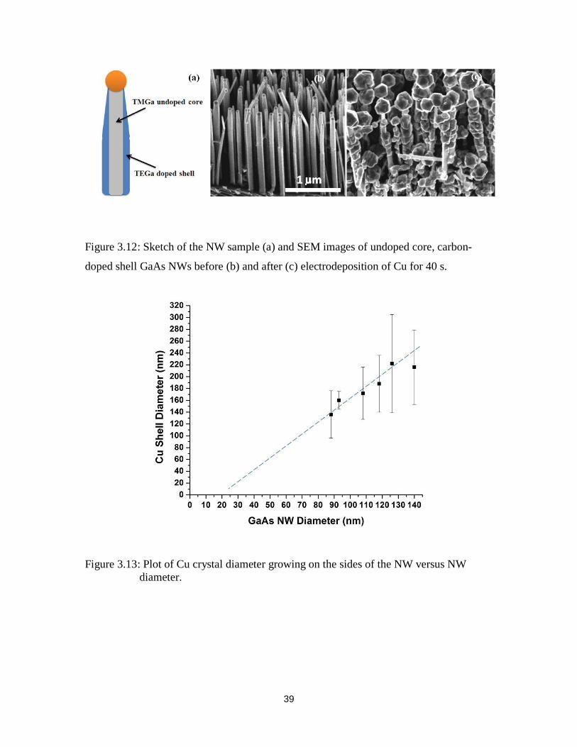
39
Figure 3.12: Sketch of the NW sample (a) and SEM images of undoped core, carbon-
doped shell GaAs NWs before (b) and after (c) electrodeposition of Cu for 40 s.
Figure 3.13: Plot of Cu crystal diameter growing on the sides of the NW versus NW
diameter.

40
3.3 Electrodeposition of Fe on GaAs nanowires
Fe was deposited onto Type A GaAs NWs grown with CBr4 for the first part of the
growth, followed by no CBr4 precursor during the last part of the growth. It was found
that tapering occurs when the carbon source is turned off [12]. As we can see in the SEM
images shown in Figure 3.14 the upper part of the GaAs NW is tapered while the lower
part is uniform in diameter. Again, Fe is only depositing on the top end of the NW where
the Au is. The SEM image shows that no Fe has grown on the smallest wires.
Figure 3.14: Sketch of the NW sample (a) and SEM images of GaAs NWs before (b) and
after (c) electrodeposition of Fe for 30 s. Tapering in the wires towards the Au end
occurred when the CBr4 was turned off in the later part of the growth.
Figure 3.15 is the plot of Fe volume versus NW diameter. We assumed again
spherical-shaped particles for the volume calculation of Fe nanoparticle. The best linear
fit has a threshold of 30 nm, indicating that there is no growth of Fe on NWs with a
diameter smaller than 30 nm.

41
Figure 3.15: Plot of calculated Fe nanoparticle volume as a function of NW diameter. The
dotted line is the best linear fit with a intercept of 30 nm.
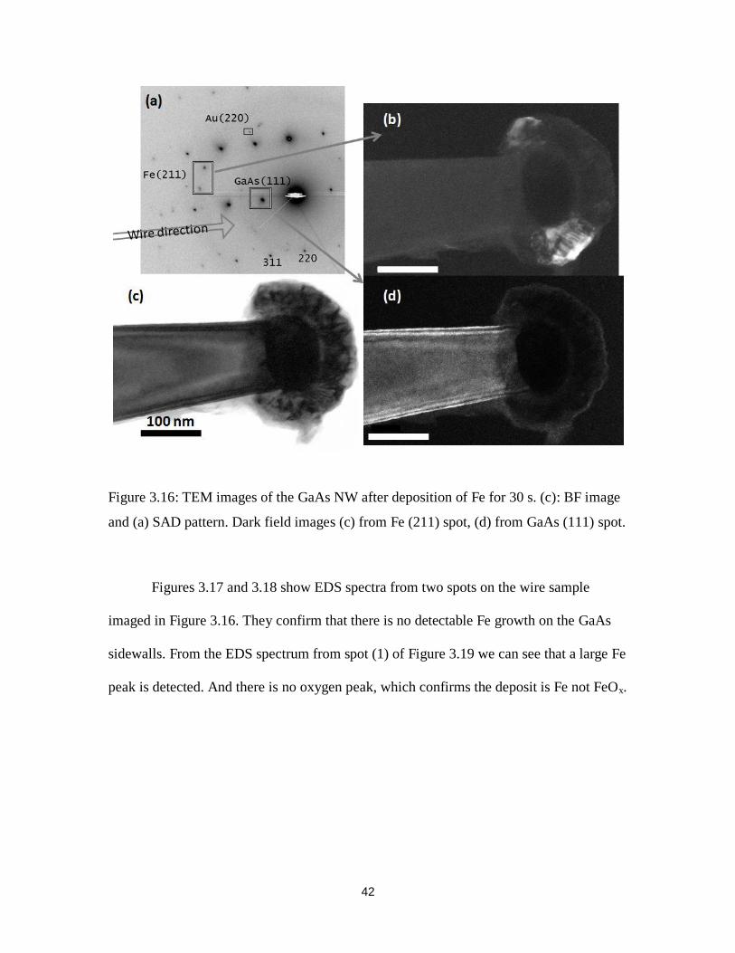
Figure 3.16 shows TEM and an associated SAD pattern for one of the nanowires
from the sample in Figure 3.14. The TEM image shows that the NW grew along a (111)
direction but that the Fe is not single crystalline. The Fe diffraction spots are indexed on
the SAD. The dark field image intensity from the Fe spot is not uniform everywhere in
the Fe region.
42
Figure 3.16: TEM images of the GaAs NW after deposition of Fe for 30 s. (c): BF image
and (a) SAD pattern. Dark field images (c) from Fe (211) spot, (d) from GaAs (111) spot.
Figures 3.17 and 3.18 show EDS spectra from two spots on the wire sample
imaged in Figure 3.16. They confirm that there is no detectable Fe growth on the GaAs
sidewalls. From the EDS spectrum from spot (1) of Figure 3.19 we can see that a large Fe
peak is detected. And there is no oxygen peak, which confirms the deposit is Fe not FeOx.
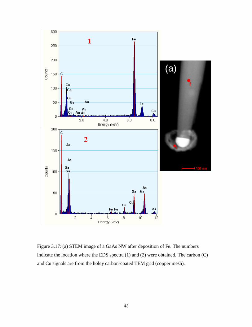
43
Figure 3.17: (a) STEM image of a GaAs NW after deposition of Fe. The numbers
indicate the location where the EDS spectra (1) and (2) were obtained. The carbon (C)
and Cu signals are from the holey carbon-coated TEM grid (copper mesh).
(a)
(a)

44
Figure 3.18: (a) A STEM image of the Au end of another wire electrodeposited with Fe.
The arrow shows the path of the focused electron probe that was used to excite x-rays
collected by the EDS detector. (b) The resulting analysis of EDS spectra as a function of
position along the arrow. We can see that the Fe region covers the Au region and the
intensities both drops to zero within 20 nm when on the GaAs wire.
The Ga signal declines towards the Au end, which is related to its decrease in
diameter. There is Ga detected in the Au. The Ga signal that overlaps the Fe signal
suggests that the Fe is growing on the wire but more likely it has simply grown out from
the Au. There is no Fe signal on the wire away from the Au.
45
3.4 Electrodeposition of metal on InAs nanowires
3.4.1 NRC InAs NWs
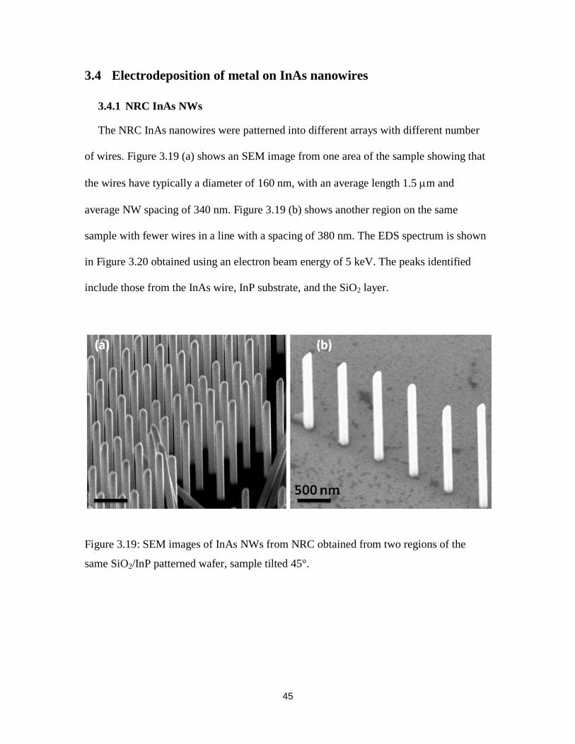
The NRC InAs nanowires were patterned into different arrays with different number
of wires. Figure 3.19 (a) shows an SEM image from one area of the sample showing that
the wires have typically a diameter of 160 nm, with an average length 1.5 m and
average NW spacing of 340 nm. Figure 3.19 (b) shows another region on the same
sample with fewer wires in a line with a spacing of 380 nm. The EDS spectrum is shown
in Figure 3.20 obtained using an electron beam energy of 5 keV. The peaks identified
include those from the InAs wire, InP substrate, and the SiO2 layer.
Figure 3.19: SEM images of InAs NWs from NRC obtained from two regions of the
same SiO2/InP patterned wafer, sample tilted 45°.
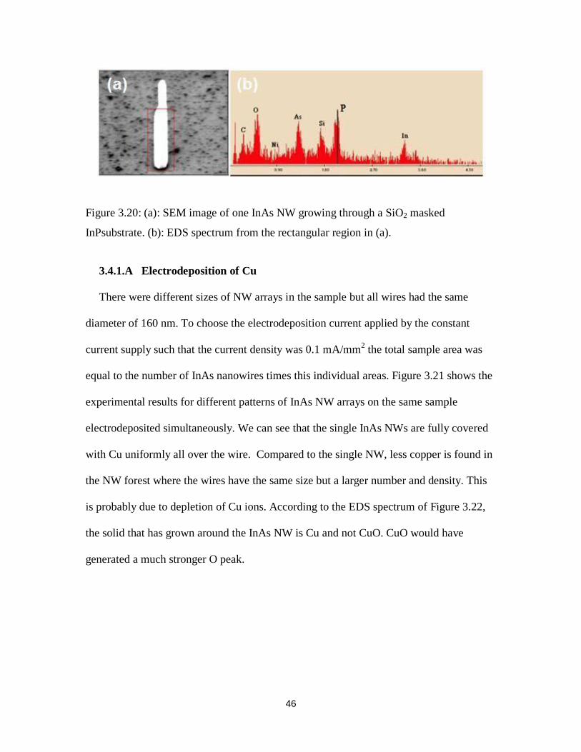
46
Figure 3.20: (a): SEM image of one InAs NW growing through a SiO2 masked
InPsubstrate. (b): EDS spectrum from the rectangular region in (a).
3.4.1.A Electrodeposition of Cu
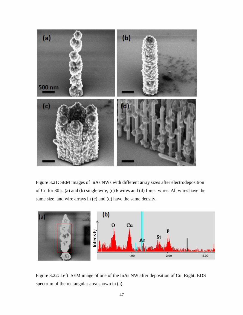
There were different sizes of NW arrays in the sample but all wires had the same
diameter of 160 nm. To choose the electrodeposition current applied by the constant
current supply such that the current density was 0.1 mA/mm2 the total sample area was
equal to the number of InAs nanowires times this individual areas. Figure 3.21 shows the
experimental results for different patterns of InAs NW arrays on the same sample
electrodeposited simultaneously. We can see that the single InAs NWs are fully covered
with Cu uniformly all over the wire. Compared to the single NW, less copper is found in
the NW forest where the wires have the same size but a larger number and density. This
is probably due to depletion of Cu ions. According to the EDS spectrum of Figure 3.22,
the solid that has grown around the InAs NW is Cu and not CuO. CuO would have
generated a much stronger O peak.
47
Figure 3.21: SEM images of InAs NWs with different array sizes after electrodeposition
of Cu for 30 s. (a) and (b) single wire, (c) 6 wires and (d) forest wires. All wires have the
same size, and wire arrays in (c) and (d) have the same density.
Figure 3.22: Left: SEM image of one of the InAs NW after deposition of Cu. Right: EDS
spectrum of the rectangular area shown in (a).
48
3.4.1.B Electrodeposition of Fe
Electrodeposition at a total current 0.001 mA (estimated current density of 0.04
mA/mm2) resulted in no evidence of deposition after 5 seconds based on SEM
investigations. In a second attempt, at a total current of 0.002 mA (current density 0.1
mA/mm2) deposition time 30 s, deposition was obtained. Figure 3.23 shows SEM images
from a single NW and a small NW array from this experiment.
Comparing this result to Cu where the same current and deposition time was used, the
Fe deposition is thinner. The cell voltage for the two depositions was different. For Cu
deposition the cell voltage is 0.60 V while for Fe it was 1.08 V. The sample for Fe
deposition was reused after the first attempt without additional cleaning. The 5 s
deposition may have caused a change in the sample surface.
Figure 3.23: SEM images (45 ° tilted) of InAs NWs after electrodeposition of Fe for 30 s.
49
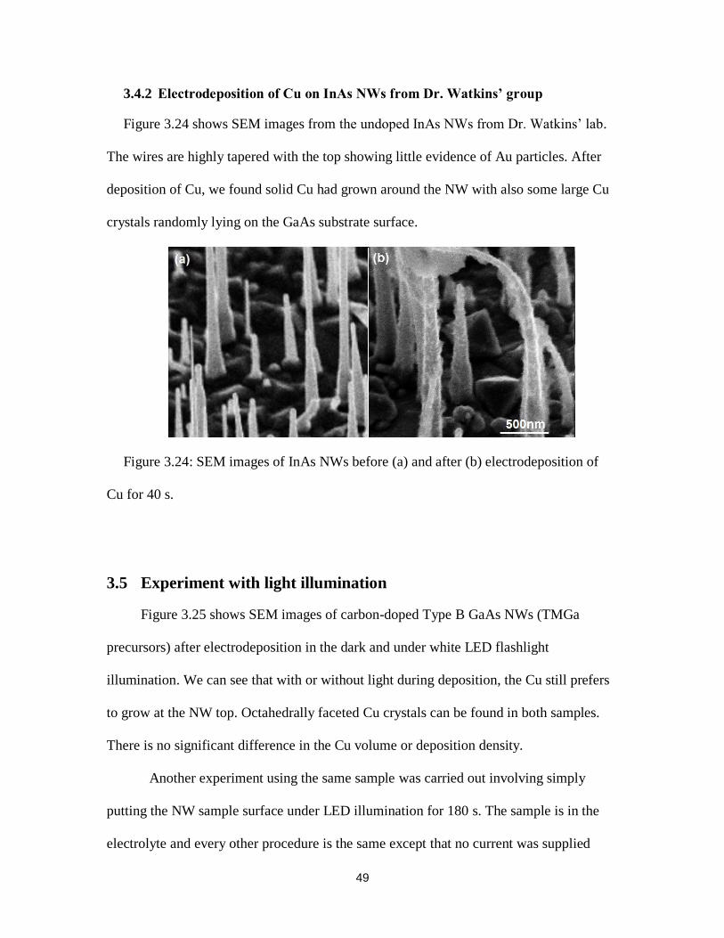
3.4.2 Electrodeposition of Cu on InAs NWs from Dr. Watkins’ group
Figure 3.24 shows SEM images from the undoped InAs NWs from Dr. Watkins’ lab.
The wires are highly tapered with the top showing little evidence of Au particles. After
deposition of Cu, we found solid Cu had grown around the NW with also some large Cu
crystals randomly lying on the GaAs substrate surface.
Figure 3.24: SEM images of InAs NWs before (a) and after (b) electrodeposition of
Cu for 40 s.
3.5 Experiment with light illumination
Figure 3.25 shows SEM images of carbon-doped Type B GaAs NWs (TMGa
precursors) after electrodeposition in the dark and under white LED flashlight
illumination. We can see that with or without light during deposition, the Cu still prefers
to grow at the NW top. Octahedrally faceted Cu crystals can be found in both samples.
There is no significant difference in the Cu volume or deposition density.
Another experiment using the same sample was carried out involving simply
putting the NW sample surface under LED illumination for 180 s. The sample is in the
electrolyte and every other procedure is the same except that no current was supplied

50
(Keithley power supply off). A certain amount of metal growth will occur simply by
providing the electrolyte. [32] SEM and EDS showed that the sample stayed the same as
before, nothing was detected to have grown on the surface.
Figure 3.25: SEM images of GaAs NWs after electrodeposition of Cu for 30 s. Left:
deposition in dark. Right: deposition under LED flashlight illumination.
3.6 Metal deposition without gold catalyst
3.6.1 Electrodeposition of Cu on gold nanoparticle samples
As a comparison experiment, we electrodeposited Cu on gold nanoparticle GaAs
samples. The gold nanoparticle sample we used had a Au particle diameter distribution
from 100 nm to 400 nm. By lowering the electrolyte beaker gradually during the
deposition, we were able to change the deposition time of deposition on different areas of
the sample in one experiment. As we can see in the series of SEM images in Figure 3.26,
at first, Cu crystals grow on a small numbers of Au nanoparticles. Then as time goes by,
more Au nanoparticles have Cu growth; finally all Au particles are covered by Cu
islands.
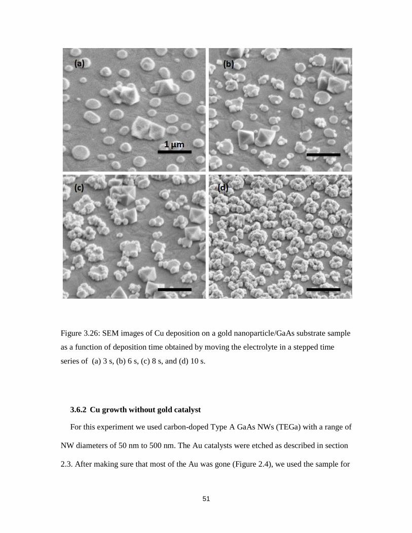
51
Figure 3.26: SEM images of Cu deposition on a gold nanoparticle/GaAs substrate sample
as a function of deposition time obtained by moving the electrolyte in a stepped time
series of (a) 3 s, (b) 6 s, (c) 8 s, and (d) 10 s.
3.6.2 Cu growth without gold catalyst
For this experiment we used carbon-doped Type A GaAs NWs (TEGa) with a range of
NW diameters of 50 nm to 500 nm. The Au catalysts were etched as described in section
2.3. After making sure that most of the Au was gone (Figure 2.4), we used the sample for

52
electrodeposition following the same procedures as samples with Au. Figure 3.27 shows
SEM images from wires showing the comparison between deposition with and without
gold catalyst. We can see that with the Au catalyst, Cu hats are found on the tops of most
NWs. In comparison, for the deposition without the Au catalyst, Cu still has a preference
for growing on top of the NW but there is less growth on NWs having diameters smaller
than 100 nm. Also, for the NWs with larger diameters, there is now more than one single
crystal growing on top. Figure 3.28 shows two NWs with diameters of 125 nm (left) and
150 nm (right). The dark part on top of the 125 nm NW could be residual Au after the
etching process. The 150 nm NW has a hexagonal-shaped Cu crystal growth on top and
the contrast indicates that there is no Au catalyst left, supported by subsequent EDS
analysis.
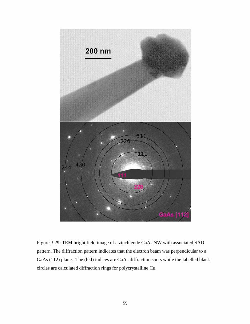
Figure 3.29 is a TEM image and associated SAD pattern from one NW with a
diameter of 200 nm. The main periodic spots in the SAD pattern index to GaAs
indicating that the NW is oriented with the electron beam perpendicular to a (112) GaAs
plane. The expected Cu spot positions are shown by the added indexed diffraction rings.
Considering the lattice mismatch between Cu and GaAs the Cu (111) atomic spacing
(0.2087 nm) is most closely matched to GaAs (220) atomic spacing (0.200 nm) with a 4%
lattice spacing mismatch. There are spots from Cu crystals that are consistent with more
than one single crystal of Cu having grown on the top of the wire, consistent with our
SEM analysis. There is no evidence of an epitaxial arrangement of the Cu on the GaAs.

53
Figure 3.27: SEM images of carbon-doped GaAs NWs (Type A) after 40 s
electrodeposition of Cu. The upper image is NWs with Au catalysts while the bottom
image is after etching the sample in an HCl: potassium-tri-iodide solution to remove the
Au catalysts.

54
Figure 3.28: TEM images of GaAs NWs where the Au was etched prior to
electrodeposition of Cu (40 s).
55
Figure 3.29: TEM bright field image of a zincblende GaAs NW with associated SAD
pattern. The diffraction pattern indicates that the electron beam was perpendicular to a
GaAs (112) plane. The (hkl) indices are GaAs diffraction spots while the labelled black
circles are calculated diffraction rings for polycrystalline Cu.
56
4: DISCUSSION
In our experiments, we have tested samples with different morphology (metal
nanoparticles on semiconductor, semiconductor NWs on top of semiconductor),
conductivity (InAs NWs and GaAs NWs with different carbon doping levels) and
structure (diameter, with and without gold catalyst at the growth end). The conductivity
and actual dopant impurity concentration in the GaAs wires investigated was unknown.
We found that metal deposition happened in different locations for different samples and
we propose that this was due to variations in the conductivity. We discuss the growth
mechanism as a function of sample surface, conductivity and morphology. COMSOL
finite element analysis was carried out to simulate the experimental results based on the
Butler-Volmer equation and Nernst-Planck equation.
4.1 Current and resistivity calculation
From the estimated Cu crystal volumes, V, as described previously in section 3.2,
we can obtain the total charge, Q, that is transferred during deposition through the
gold/electrolyte interface given by:
(4.1)
where ρ is the atomic density of Cu, Ar is atomic weight and NA is Avogadro’s number, z
= 2 is the Cu ion valence. The total charge divided by the deposition time will give us the
average current through the NW. The challenging part for further calculation of the NW
resistance is that we do not know the voltage drop across the length of the NW. If we

57
ignore the voltage drop of the outer cell circuit (which is very small), our system
primarily measures the potential drop between the cathode and anode. The n-type GaAs
substrate and p-type C-doped GaAs NW interface is a forward biased p-n junction during
deposition. Since the cathode is platinum and the anode wafer is heavily-doped n-type
GaAs (350 ± 25 m thickness), the voltage drop mainly occurs inside the semiconductor
NW, the Helmholtz layer and the electrolyte. To make a rough approximation, we
assumed 1.5 V out of the total 2 V voltage drop as the potential difference across the
NW, from the NW base at the wafer surface to the gold tip. From TEM or SEM images
we can measure the length and diameter of NWs, and then use
(4.2)
for resistivity estimates.
Data for Cu volume versus NW diameter for the intentionally carbon-doped
sample discussed in section 3.2.1 (type A) was shown in Fig. 3.9. This was used to
calculate the average current and resistivity as a function of GaAs NW diameter via
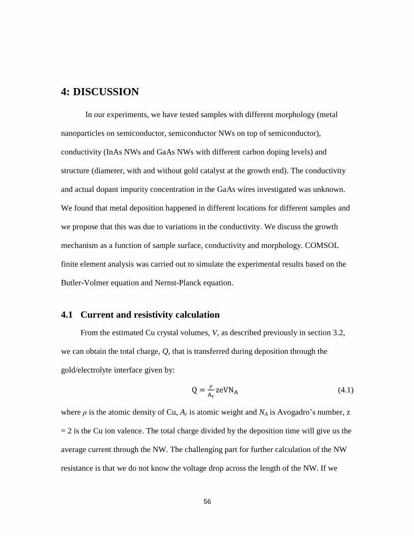
equations 4.1 and 4.2, respectively. . The current increases, up to 2.5 pA as the diameter
increases. The 52 nm diameter NWs were more conductive than the 60 nm-90 nm ones,
which might be due to a higher doping level [33]. Figure 4.1(b) is a plot of current versus
NW cross-sectional area. The slope of the best linear fit line gives us the average current
density, which is 0.24 ± 0.09 mA/mm2, the same order of magnitude as the applied
current density (total current divided by sample area times 40%, 0.1 mA/mm2). The
calculated average resistivity was 2 1 x 10⁴ Ωm, equivalent to bulk GaAs with a very
low carrier density ~1010
cm-3
[34].
58
Figure 4.1: (a) NW current (solid circle point) and calculated resistivity (dashed square
point) versus NW diameter and (b) current versus NW cross-sectional area for Cu
deposition on carbon-doped GaAs NWs (type A) (section 3.2.1). The dashed line is the
best linear fit with slope 2.4 ± 1 x10⁻⁴
pA/nm2 (average current density
: 0.2 ± 0.1
mA/mm2 )
(a)
(b)

59
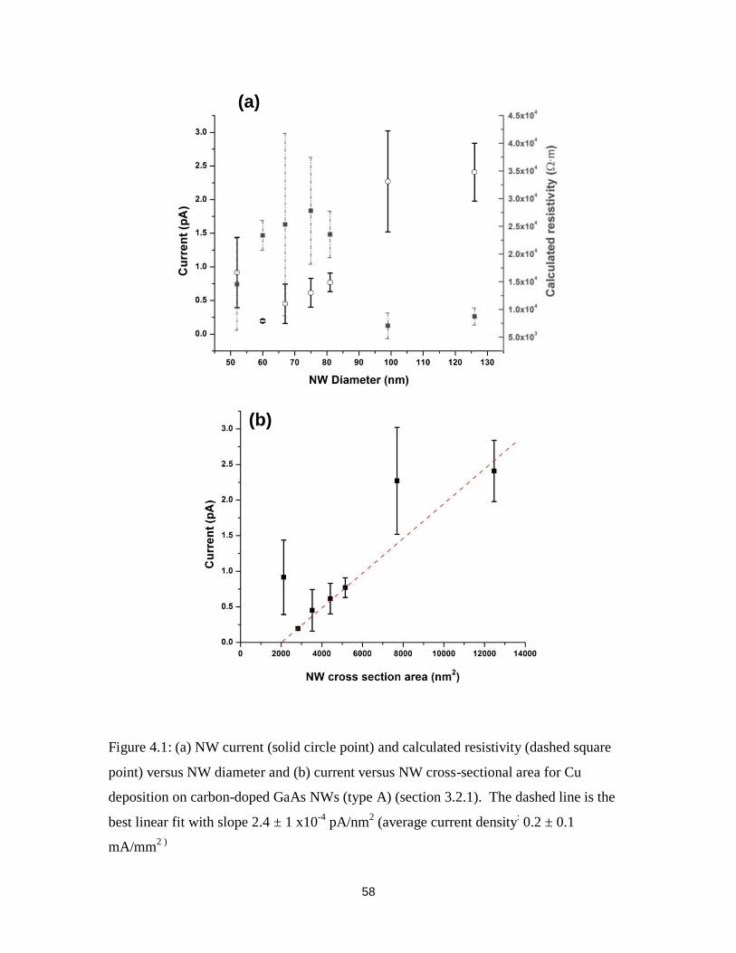
Figure 4.2 shows the calculated current and resistivity for the Fe-deposited NWs
grown on type A NWs with CB4 doping for the initial part of the MOVPE growth, as
discussed in section 3.3. In Figure 4.2 (a) the current increases up to 5.5 pA as the
diameter increases. The intercept at 30 nm indicates that deposition on NWs with
diameters smaller than 30 nm did not occur. From the slope of Figure 4.2 (b) the
calculated average current density is 0.17 ± 0.05 mA/mm2. The calculated average
resistivity for this sample is also ~104 Ωm.
The same calculation was carried out using the Cu volume measurements from
Cu-deposited onto undoped GaAs NWs (type A) described in section 3.1.1). The average
current through these wires was 0.8 pA and the calculated resistivity is therefore, 2400 ±
900 Ωm, equivalent to bulk GaAs with a carrier density ~1011
cm-3
. The undoped wires
are apparently slightly more conductive than those that were intentionally carbon-doped
based on this model calculation. . It has been reported that the resistivity of VLS grown
undoped GaAs NW is ~ 500 Ωm by transmission-line I-V measurement [35] comparable
to our result. However, it is unlikely that the level of dopant impurities in our wires was
less than typcial values for planar grown MOVPE GaAs (~1016
/cm3). The calculated high
resistivity indicates that all NWs grown with or without CBr4 with diameters under 200
nm discussed in this section were likely fully depleted. We will discuss the depletion
width in more detail in section 4.3.1.

60
61
Figure 4.2: (a) Calculated current versus NW diameter and (b) NW cross-sectional area
for Fe deposition on intentionally carbon-doped followed by undoped type A GaAs NWs
(section 3.3). The dashed line in (b) is the best linear fit with slope of 0.17 ± 0.05
mA/mm2. (c) Plot of the calculated resistivity as a function of NW diameter.
4.2 COMSOL simulation
To better explain the deposition results, finite element simulation was carried out
using COMSOL® Multiphysics. We started with the simplest situation: the deposition
process for a quasi-metal (InAs) NW without a gold catalyst. The model was built with
the Chemical Engineering Module using the Nernst-Planck equation. [36] We simulated
the electric field distribution for our electrochemical cell as applied to GaAs NWs using
the AC/DC Module.
62
4.2.1 Cu deposition on InAs NWs
For the NRC InAs NWs sample, there were no gold catalysts. NWs grew from the InP
substrate via openings in a deposited SiO2 insulating layer. InAs NWs are naturally
highly conductive due to their smaller bandgap (0.36 eV) and a surface accumulation
layer [37]. All of these facts made the system easier to simulate.
The model system is designed by using the material balance for the ions involved:
Cu2+
and SO42-
and the electroneutrality condition. The model geometry is depicted in
Figure 4.3. The cell is fully filled with electrolyte. The anode is represented by the upper
horizontal boundary while the cathode substrate is placed at the bottom a distance 30 μm
away from the anode.
To make the model simple and not introduce other ions, we used Cu as the anode
material. Thus, it is a copper dissolution process (reverse of deposition) on the anode. For
the cathode, only the InAs NW portion of the sample has a current distribution. The
vertical walls of the model cell are assumed to be insulating similar to the glass container
of the real cell.
The flux of ions in the electrolyte is given by the Nernst-Planck equation [9]:
(4.3)
where Ni denotes the flux of moving ions (mole m-2
s-1
), Di is the ion diffusivity (m s-2
),
ci the concentration of ion in the electrolyte (mole m-3
), zi the charge on the ionic species,
ui the mobility of the charged species (m2s
-1J
-1mole
-1) , F Faraday’s constant (As mole
-1)
and the potential in the electrolyte (V). The material balance is expressed by:
. (4.4)
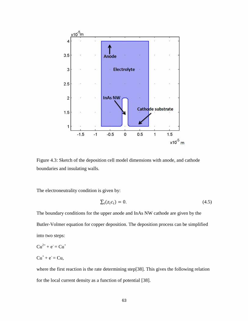
63
Figure 4.3: Sketch of the deposition cell model dimensions with anode, and cathode
boundaries and insulating walls.
The electroneutrality condition is given by:
. (4.5)
The boundary conditions for the upper anode and InAs NW cathode are given by the
Butler-Volmer equation for copper deposition. The deposition process can be simplified
into two steps:
Cu2+
+ e- = Cu
+
Cu+
+ e- = Cu,
where the first reaction is the rate determining step[38]. This gives the following relation
for the local current density as a function of potential [38].
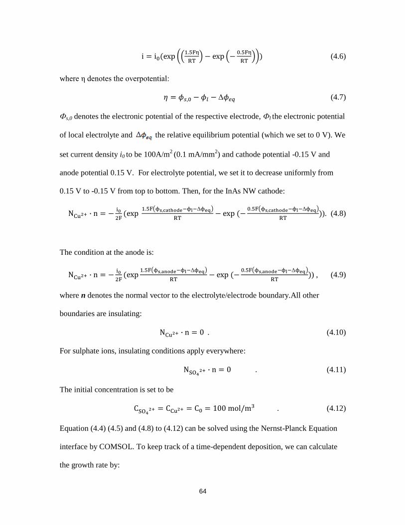
64
(4.6)
where η denotes the overpotential:
(4.7)
Фs,0 denotes the electronic potential of the respective electrode, Фl the electronic potential
of local electrolyte and the relative equilibrium potential (which we set to 0 V). We
set current density i0 to be 100A/m2 (0.1 mA/mm
2) and cathode potential -0.15 V and
anode potential 0.15 V. For electrolyte potential, we set it to decrease uniformly from
0.15 V to -0.15 V from top to bottom. Then, for the InAs NW cathode:
). (4.8)
The condition at the anode is:
) , (4.9)
where n denotes the normal vector to the electrolyte/electrode boundary.All other
boundaries are insulating:
. (4.10)
For sulphate ions, insulating conditions apply everywhere:
. (4.11)
The initial concentration is set to be
. (4.12)
Equation (4.4) (4.5) and (4.8) to (4.12) can be solved using the Nernst-Planck Equation
interface by COMSOL. To keep track of a time-dependent deposition, we can calculate
the growth rate by:

65
, (4.13)
where M denotes molar mass. The moving boundaries are treated through an arbitrary
lagrangian eulerian (ALE) method incorporated inside COMSOL.
Simulation results
Figure 4.4 shows the simulation results after 1 s of deposition. The deposited Cu is
represented by the blank part between the original domain boundary and the colourful
mesh. From Figure 4.5 we can see that, as time goes by, the tip region has a slightly
greater copper growth compared to the bottom. After 5 s deposition the simulation shows
greater copper thickness at the tip compared to other parts, but the difference is relatively
small. From the isopotential lines around the NW we can tell that the top part is denser
which means a larger electric field. The model results tell us that if we have quasi-metal
NWs (without gold catalysts) in the electrochemical system, under reasonable
overpotential, Cu will deposit uniformly around the NW without a significant preference
for the tip.
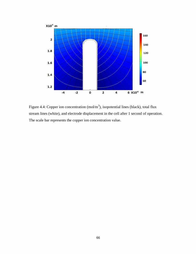
66
Figure 4.4: Copper ion concentration (mol/m3), isopotential lines (black), total flux
stream lines (white), and electrode displacement in the cell after 1 second of operation.
The scale bar represents the copper ion concentration value.

67
Figure 4.5: Copper ion concentration (mol/m3), isopotential lines, total flux stream lines,
and electrode displacement in the cell after (a) 2 s, (b) 3 s, (c) 4 s and (d) 5 s of operation.
The scale bar represents the copper ion concentration value.
4.2.2 Electric field simulation for low conductivity GaAs NWs
For low conductivity GaAs NWs samples, there is no basic theory available to predict
current flow when we have both semiconductor and metal as the nanoscale electrode. We
found Cu only deposited around the NW bottom and at the top for the undoped and
intentionally-doped GaAs NWs presented in 3.1.2 and 3.2.2. Also we found that Cu still
had a preference for growing on the top even after we etched away the gold catalysts for
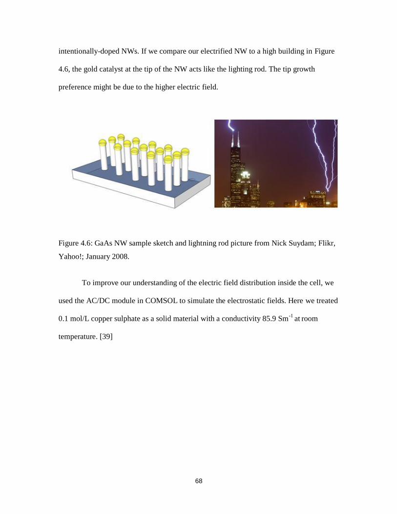
68
intentionally-doped NWs. If we compare our electrified NW to a high building in Figure
4.6, the gold catalyst at the tip of the NW acts like the lighting rod. The tip growth
preference might be due to the higher electric field.
Figure 4.6: GaAs NW sample sketch and lightning rod picture from Nick Suydam; Flikr,
Yahoo!; January 2008.
To improve our understanding of the electric field distribution inside the cell, we
used the AC/DC module in COMSOL to simulate the electrostatic fields. Here we treated
0.1 mol/L copper sulphate as a solid material with a conductivity 85.9 Sm-1
at room
temperature. [39]
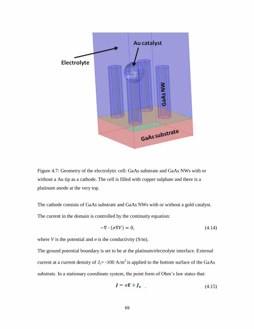
69
Figure 4.7: Geometry of the electrolytic cell: GaAs substrate and GaAs NWs with or
without a Au tip as a cathode. The cell is filled with copper sulphate and there is a
platinum anode at the very top.
The cathode consists of GaAs substrate and GaAs NWs with or without a gold catalyst.
The current in the domain is controlled by the continuity equation:
, (4.14)
where V is the potential and σ is the conductivity (S/m).
The ground potential boundary is set to be at the platinum/electrolyte interface. External
current at a current density of Je= -100 A/m2 is applied to the bottom surface of the GaAs
substrate. In a stationary coordinate system, the point form of Ohm’s law states that:
. (4.15)

70
. (4.16)
As shown is Fig 4.9, copper sulphate is filled in the cell and the outer boundaries of the
domain are insulating:
. (4.17)
The conductivity of the n+ GaAs substrates is set to 105 S/m (10
18cm
-3 doping level) and
the GaAs NWs to low or high conductivities between of 10-3
S/m and 106 S/m,
respectively.
Simulation results
Fig 4.8 shows the simulation results for two non-conductive GaAs NWs the left
one with Au and the right one without Au. We can see that very low current goes through
the NWs because the electrolyte is more conductive than the wire in this situation. The
electric field is largest at the top part for both NWs with Au and without a Au catalyst.
Figure 4.9 shows the simulation results for conductive GaAs NWs with and
without a Au catalyst. The current through the wires is much larger than the current
through the electrolyte. The electric field is larger at the top part as well as at the bottom
around the NW, which is consistent with our experimentally observed Cu nucleation sites
as shown in Figure 3.11. Also the Au catalyst of the left NW attracts more current
compared to the one without a Au catalyst on top at right. This model is producing results
that more closely match our experiment. The corners at the NW/substrate interface will
cause a higher electric field around the bottom of the NW.

71
Figure 4.8: Simulation results of (a) current density (A/m2) and (b) electric field (V/m)
distribution in the cell for GaAs NWs with low conductivity 10-3
S/m with and without a
Au catalyst.

72
Figure 4.9: Simulation results of (a) current density (A/m2) and (b) electric field (V/m)
distribution in the cell for GaAs NWs with conductivity 106 S/m with and without a Au
catalyst.

73
4.3 Other factors important to metal nucleation
4.3.1 Geometry and depletion width
From Fig 3.10 we saw that for type A GaAs NWs with large diameters (~1 m)
copper also nucleated and grew on the GaAs sidewalls NW, right below the Au tip.
Conversely, referring to Fig 3.14, we did not find Cu growth on greatly tapered NWs.
Furthermore, from measurements of Cu or Fe volume versus wire diameter there was a
threshold wire diameter below which the metal did not form. If the wires were of
identical conductivity and length then the current density would have been the same.
However, the total current available for nucleation will eventually be too small for
smaller wires for nucleation to succeed. Alternatively, if the wire conductivity is a
function of diameter decreasing with decreasing size, then smaller wires would become
too resistive for nucleation. Although the electric field is theoretically higher at smaller
wire tips, their shrinking cross-sectional area and increasing resistance, lowers the
available current.
On the other hand, the sidewall Cu growth of the type A GaAs NWs with large
diameters (~1 m) in Fig 3.10 means these wires with large diameter are more
conductive than the wires with small diameters, which indicates that they are not fully
depleted. Thus, the depletion width is between 65 nm and 400 nm if we assume there is a
200 nm conductive core for the 1 m diameter wire. The depletion width for GaAs NWs
can be calculated as [40]:
, (4.18)
where n is the concentration of charge carriers, εr = 13.1 is the relative permittivity of
GaAs and Vs = 0.45 V is the surface potential for p-GaAs [41]. If we reverse the
74
calculation assuming d = 65 to 400 nm we get a carrier concentration in the range of 3.7
x 1015
cm-3
and 1.4 x10¹⁷
cm-3
. If we do the same calculation for the core-shell GaAs
NWs discussed in 3.2.3, whose depletion width should be smaller than 40 nm, the relative
calculated carrier concentration is larger than 3 x 10¹⁷
cm-3
. These values for the actual C-
dopant impurity concentration for CBr4 MOVPE growth are more consistent with planar
results.
4.3.2 Gold catalysts
In section 3.6.2 we showed that Cu still prefers to grow on the ends of the NW even
after we etched off the Au catalysts. This indicates that either the gold was not all
removed or that gold is not necessary for the Cu tip nucleation. However, we do see Cu
nucleation on NWs of smaller diameters (< 100 nm) with Au catalysts still there, which
we do not see as frequently for NWs of the same diameter without Au catalysts. This is
again likely due to the increased conductivity of Au versus the semiconductor , as
discussed in section 1.2. Without a Au catalyst on the top end, the NW still has to face a
depletion region at the semiconductor/electrolyte interface. The current of the smaller
diameter NW is not large enough to form a stable nucleus.
4.3.3 Overpotential
Cu electrodeposition is reversible, but there is a minimum nucleus size necessary for
continued metal growth [42]. The number of Cu ions, N, in each critical nucleus is a
function of the overpotential:
(4.19)

75
where s is the area of one metal atom, and z is the number of electrons each ion carries (2
for Cu2+
). We can see that the size of the critical cluster will decrease as the overpotential
increases. On the other hand, if we apply an extra high overpotential, the current through
the NW will increase, thus increasing the number of electrons that tunnel through the
depletion barrier.
Figure 4.10 shows the experimental results for Cu deposition on GaAs NWs with
an extra large current density, i.e. large overpotential. Cu growth can be detected around
the NW extending into dendrites growing out the top of the NW.
Figure 4.10: SEM image of GaAs NWs after Cu deposition for 5 s with 40
mA/mm2 current density and relative EDS spectrum from two different spots of the
GaAs NW.

76
4.4 Sample surface
In this section, we focus on the chemical composition of the electrode surface in our
experiments.
4.4.1 Surface oxidation
A previous report found Ni growth only on the Au catalysts at the top end of P-doped
Si NWs. After removing the Si NW surface oxide (1% HF), they found Ni particles also
deposited along the sidewalls of the NWs [43]. They concluded that the surface oxide on
their p-doped Si NWs, acted as an insulating layer which prevented metal deposition on
the sidewalls.
In our experiment, a dilute ammonium hydroxide solution was used to etch the GaAs
NW surface oxide. Contact angle measurements indicated that the resulting surfaces of
the NW samples were then hydrophilic. Yet for the unintentionally-doped GaAs NWs,
Cu electrodeposition also occurred predominantly only at the Au ends of the wire. Was
this due to poor oxide etching, poor wetting of the NWs by the electrolyte, or simply poor
NW conductivity? Evidence that the electrolyte reached the substrate is that Cu
electrodeposition was also visible at the bottom of unintentionally-doped GaAs NWs.
Once the wires were of higher conductivity, including the core-shell doped GaAs NWs
and InAs NWs, we found Cu growth around the sidewalls to the substrate. This further
supports the conclusion that surface oxides were removed by ammonium etching in all
cases, and that the NWs were completely immersed in the electrolyte for both InAs and
GaAs NWs. Variations in the location of metal growth were due to variations in wire
conductivity.

77
We know GaAs in the ambient environment forms a layer of native oxides, a mixture
of Ga2O3 and As2O3. This electrically insulating layer could inhibit or prevent entirely
sidewall Cu growth. Also gold does not oxidize in air or water. Thus, as a suggestion for
a future experiment, leave the oxide on the wire, remove organic impurities with ethanol
instead of ammonium hydroxide, then tip only deposition should be feasible.
4.4.2 Incorporation of carbon
Our results indicate that Cu grows only around the Au catalyst at the top end of
undoped GaAs NWs and doped GaAs NWs, while Cu grew along the length of core-shell
doped GaAs NWs. The most likely conclusion is that the degree of carbon doping that
occurs during the VLS NW growth is much lower than during the growth of a shell onto
an existing GaAs core. In VLS-doped NWs the carbon concentration is too low to make
sufficient difference to the conductivity.
4.5 Cu contact for I-V measurement
The initial purpose of this project was to make ohmic contacts for NW I-V
measurements. A tungsten probe tip was installed inside the SEM so that individual wires
could be contacted. The probe radii are about 150 nm, much larger than the diameter of
most of our GaAs NWs. Fig 4.11 shows that a large copper contact provides a larger
contact surface, makes the contact process easier and more visible, compared to trying to
contact the smaller Au catalyst directly without a copper contact. Measurements of I-V
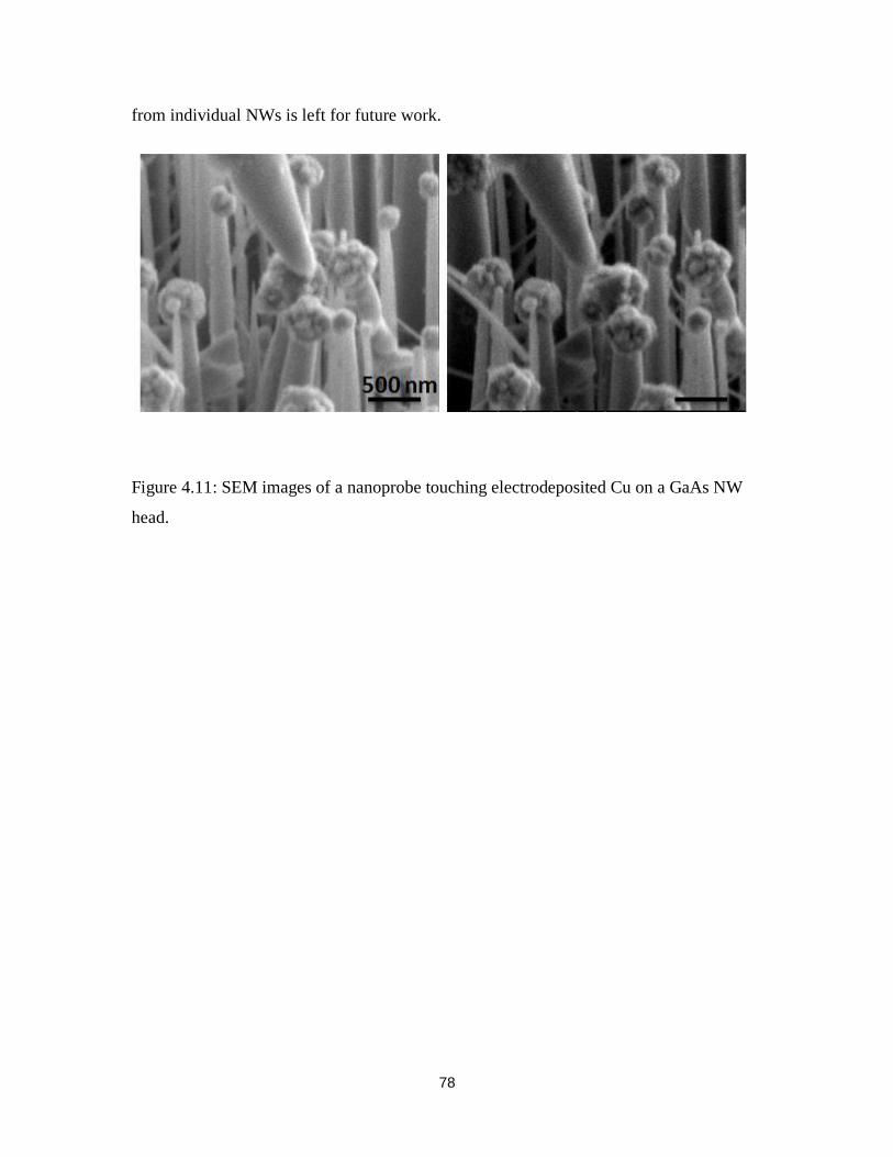
78
from individual NWs is left for future work.
Figure 4.11: SEM images of a nanoprobe touching electrodeposited Cu on a GaAs NW
head.

79
5: SUMMARY
For low-doped (non-conductive) NWs, both COMSOL simulation and
experimental results find that electrodeposition happens at the top part of the NW, as
shown in Figure 5.1. This preferential growth is due to a large depletion region barrier on
the semiconductor sidewalls and the higher electric field on the NW top. The top growth
preference did not change when we removed the gold catalyst, as shown in Figure 3.27.
The square in the figure is the sample substrate while the grey bar represents a low-doped
NW. The deposited metal is represented by the darker regions.
Figure 5.1: Sketch of low-doped NW sample before and after electrodeposition.

80
For our individual GaAs NW samples, we found Cu or Fe grows preferentially on
top of the gold particles used for GaAs nanowire growth. Copper was epitaxial whereas
iron was randomly oriented. Removal of the gold catalyst did not change the location of
preferential growth.
Sidewall deposition on low-doped NWs can be achieved by applying higher
current density (higher overpotential) within a short time. Three electrode systems are
required for further investigation of the relationship between cathode overpotential,
deposition time and film thickness.
For highly-doped (conductive) NWs, we would expect metal deposition
everywhere around the wire, and a large head growth if there is a Au catalyst at the end,
as shown in Figure 5.2. Sidewall metal growth should be prevented by keeping the
native-oxide film around the nanowire. For GaAs NW sample, this might be achieved by
etching the sample with ethanol instead of ammonium hydroxide right before deposition.
Future experiment needs to be done to test this.
Figure 5.2: Sketch of highly-doped NW sample before and after electrodeposition.

81
A summary of the experimental results regarding metal nucleation locations for
all samples investigated is shown in Table 2.1.
Through our experiment on GaAs NWs, we can conclude that direct carbon-
doping of GaAs shell layers is more effective than carbon-doping via the Au catalyst (C-
doped Type A or B). The effective resistivity of the undoped and CBr4 doped NWs was
estimated to be 103 Ωm and 10
4 Ωm, respectively, limited by surface depletion. Three
electrode, potentiostatic electrodeposition systems might be useful for a more precise
control of GaAs surface voltage, and thus rate of metal nucleation.
82
APPENDICES
Appendix A : Potential time relation
The potential drop across the deposition cell has been recorded during
electrodeposition. Figure A. 1 shows plots of potential versus time for seven different
experiments. We can see that it usually takes 2~3 seconds for the voltage to become
stable. The voltage change for Au nanoparticle samples was different compared to the
NWs whether GaAs or InAs. The potential dropped abruptly during the first 8 s then
gradually decreased further to a stable value. While for all other samples, the potential
dropped to a minimum value at the first 5 s as we immersed our samples into the
electrolyte, and then increased gradually towards a constant value likely due to the
establishment of diffusion-limited Cu ion transport in the electrolyte. This difference
might be due to the nature of the electrolyte diffusion profiles for a flat substrate
compared to nanowires. Another factor might be that the contact area of the Au
NP/semiconductor interface increases as deposition goes on if Cu began to deposit
directly on the GaAs substrate.

83
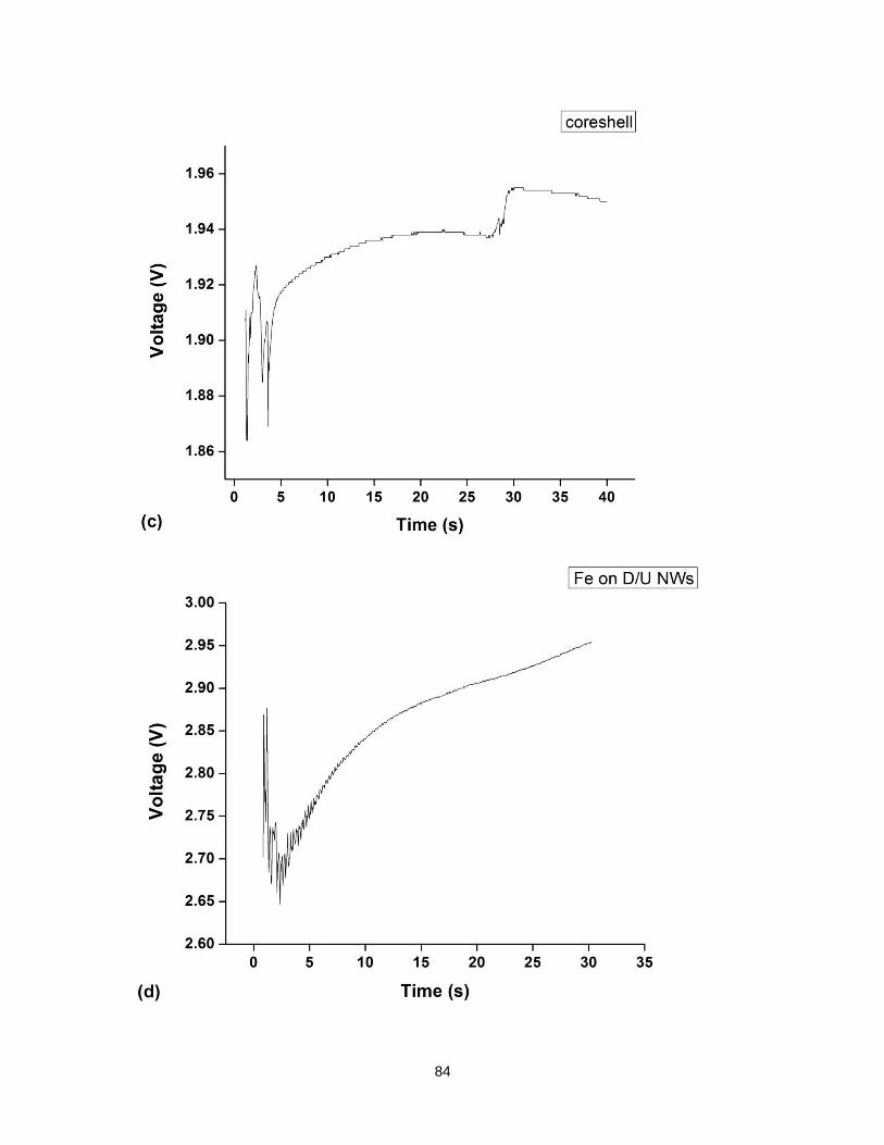
84

85

86
Figure A.1: Potential change as a function of deposition time for: (a) Cu
deposition on Type B GaAs NWs with CBr4 or without CBr4, (b) Cu deposition on
Type B GaAs NWs with CBr4 in the dark or illuminated with a LED flashlight, (c)
Cu deposition on core shell GaAs nanowires. The sample was lifted up a bit (thus
reaction area decreased) at 27 s after the start of deposition. (d) Fe deposition on
Type A doped/undoped GaAs NWs. (e) Cu deposition on InAs NWs from NRC.
(f) Cu deposition on Au nanoparticle samples with 2 nm and 5 nm Au thickness
before annealing and (g) Fe deposition on GaAs bulk samples.

87
BIBLIOGRAPHY
[1] M. Bockrath, D. H. Cobden, P. L. McEuen, N. G. Chopra, A. Zettl, A. Thess, and R.
E. Smalley, Science 275, 1922 (1997).
[2] Y. Cui, X. Duan, J. Hu, and C. M. Lieber , J. Phys. Chem. B 104, 5213 (2000).
[3] Stephen B. Cronin, Yu-Ming Lin, Oded Rabin, Marcie R. Black, Jackie Y. Ying,
Mildred S Dresselhaus, Pratibha L Gai, Jean-Paul Minet and Jean-Paul Issi,
Nanotechnology 13, 653 (2002).
[4] S.Ingole, P.Aella, S.J.Hearne, and S.T.Picraux, Appl. Phys. Lett. 91, 033106 (2007).
[5] S.Ingole,P.Manandhar, J.A.Wright, E.Nazaretski, J.D.Thompson, and S.T.Picraux,
Appl. Phys. Lett. 94, 223118 (2009).
[6] Hohn OM. Bockris, Amulya K.N.Reddy, Maria Gamboa-Aldeco, Modern
Electrochemistry, 2nd edition, Kluwer Academic (1998).
[7] John C. Kotz, Paul Treichel and Gabriela C. Weaver, Chemistry and chemical
reactivity, Cengage Learning (2006).
[8] Michio Okamura, Electric Double Layer Capacitors and Power Storage Systems,
Nikkan Kogyo Shimbun Ltd. (2001).
[9] Santos, Elizabeth and Schmickler, Interfacial electrochemistry, 2nd edition, Springer
(2010).
[10] Z. L. Bao, S. Grist, S. Majumder, L. B. Xu, E. Jensen, and K. L. Kavanagh, J.
Electrochem. Soc. 156 (2009) D138.
[11] Zhi Liang Bao, K. L. Kavanagh , J. Appl. Phys. 98, 066103 (2005).

88
[12] O Salehzadeh and S P Watkins, Nanotechnology 22, 165603 (2011).
[13] O. Salehzadeh, S.P. Watkins, J. Crystal Growth 325, 5 (2011)
[14] T.S.Chow, J. Phys.: Condens. Matter, 10, 27 (1998).
[15] Yu-Hung Cheng, C.K Chou, C. C. Chen, and S.Y.Cheng, Chem. Phys. Lett. 397, 17
(2007).
[16] C.-T. Lee, K.-L. Jaw and C.-D. Tsai, Solid-State Electronics 42, 871 (1998).
[17] S. Osakabe and S. Adachi, J. Electrochem. Soc. 144, 290 (1997).
[18] K. Sefiane , L. Tadrist, and M. Douglas, Int J Heat Mass Tran 46, 4527 (2003).
[19] Don W.Green and Robert H.Perry, Perry’s Chemical Engineer’s Handbook,
McGraw-Hill Professional (1984).
[20] MicroChemicals, Germany “Wet Chemical Etching of Gold.”
http://www.microchemicals.eu/technical_information
[21] B.L. Weiss, J. Mater Sci. 11, 1596 (1976).
[22] Jacob H. Woodruff, Joshua B. Ratchford, Irene A. Goldthorpe, Paul C. McIntyre,
and Christopher E.D. Chidsey, Nano Letters 7,1637 (2007).
[23] S. Thunich, L. Prechtel, D. Spirkoska, G. Abstreiter, A. Fontcuberta i Morral, and
A. W. Holleitner, App. Phys. Lett. 95, 08311( 2009).
[24] Raffaella Calarco, Michel Marso, Thomas Richter, Ali I. Aykanat, Ralph Meijers,
Andre´ v.d. Hart, Toma Stoica, and Hans Luth, Nano Letts 5, 981 (2005)
[25] Ronald H. Micheels, Allan D. Darrow and R. David Rauh, Appl. Phys. Lett. 39, 418
(1981).
[26] Saulius J, Akira Y, Hidekazu I, Shigeki M, Hitoshi T, and Hiroaki M, Jpn. J .Appl.
Phys. 40, 4246 (2001) .

89
[27] Hung-Chun Lo, Yi-Fan Huang, Surojit Chattopadhyay, Chih-Hsun Hsu, Chia-Fu
Chen, Huei-Hsien Chen and Li-Chyong Chen Nanotechnology 17, 2542 (2006).
[28] David B.Williams and C. Barry Carter, Transmission Electron Microscopy, Plenum
Press (1996).
[29] Yang Tang, Dongxu Zhao, Jie Chen, Nelia Wanderka, Dezhen Shen, Fang Fang,
Zhen Guo, Jiying Zhang, and Xiaohua Wang, Mater Chem Phys. 121, 541 (2010).
[30] Justin J. Hill, Kelly Haller, Brittany Gelfand, and Kirk J. Ziegler, ACS Appl. Mater.
2, 1992 (2010).
[31] MTchernycheva, J C Harmand, G Patriarche, L Travers and G E Cirlin,
Nanotechnology 17, 4025 (2006).
[32] Taleb Mokari, Eli Rothenberg, Inna Popov, Ronny Costi and Uri Banin, Science,
304, 1787(2004).
[33] O.S. Einabad. Carbon doping of GaAs nanowires. Master’s Thesis, Department of
Physics, Simon Fraser University, 2010.
[34] S.M. Sze and J.C. Irvin, Solid State Electronics 11, 599 (1968).
[35] Michael J. Tambe, Shenqiang Ren, and Silvija Gradecˇak, Nano Letts. 10, 4584
(2010).
[36] COMSOL Model Gallery, “Copper deposition in a trench”
http://www.comsol.fi/showroom/gallery/2112/
[37] Alexandra C. Ford, Johnny C. Ho, Yu-Lun Chueh, Yu-Chih Tseng, Zhiyong Fan,
Jing Guo, Jeffrey Bokor and Ali Javey, Nano Lett., 9, 360 (2009).
[38] E.Mattson and J.O’M. Bockris, Trans. Far. Soc. 55, 1586 (1959).
[39] Marija Besˇter-Rogac, J. Chem. Eng. Data 53, 1355 (2008).
90
[40] D. Stichtenoth, K. Wegener, C. Gutsche, I. Regolin, F. J. Tegude, W. Prost, M. Seibt
and C. Ronning. Appl. Phys. Lett. 92, 163107 (2008).
[41] L. G. Meiners, Appl. Phys. Lett. 33, 747 (1978).
[42] A.A. Yasseri, S. Sharma, T.I. Kamins, Z. Li and R. Stanley Williams, Appl. Phys. A.
82, 659 (2006).
[43] Ingole, S. Manandhar, P. Wright, J. A. Nazaretski, E. Thompson, J. D. Picraux, S.
T. Appl. Phys. Lett, 94, 223118 (2009).