Electrochromic properties and coloration mechanisms of sol ...
172
Electrochromic properties and coloration mechanisms of sol-gel NiO-TiO 2 layers and devices built with them Dissertation Zur Erlangung des Grades Doktor der Wissenschaften An der Naturwissenschaftlich-Technischen Fakultät III Der Universität des Saarlandes Vorgelegt von Amal Alkahlout Saarbrücken 2006
Transcript of Electrochromic properties and coloration mechanisms of sol ...
Electrochromic properties and coloration mechanisms of
sol-gel NiO-TiO2 layers and devices built with them
Dissertation
Zur Erlangung des Grades
Doktor der Wissenschaften
An der Naturwissenschaftlich-Technischen Fakultät III
Der Universität des Saarlandes
Vorgelegt von
Amal Alkahlout
Saarbrücken
2006
Tage des Kolloquims: Dekan: Professor Dr. Kaspar Hegetschweiler Berichterstatter: Professor Dr.Michel A. Aegerter Berichterstatter: Professor Dr. Wulff Possart Vorsitzender: Professor Dr. Michael Veith Beisitzer: Dr. Andreas Rammo

Dedicated to my own soul out of my soul ….Mustafa

I
Acknowledgment
GOD...without your help and support, I could not survive or achieve any thing. First, I thank Professor Dr. M.A. Aegerter for giving me the chance to be one of his students and for his generous advices, valuable discussions which helped me greatly, and the good proof reading of this thesis. He did not only guide this work and find time to discuss with me but also gave me the confidence to express my ideas freely. I will always remember how his ideas and suggestions always work and how he could simply pick the small mistakes. I am also most grateful to him for giving me the chance to have realized some scientific work at the university of São Paulo in São Carlos (Brazil). I have to say that your presence at INM is the best thing could happen to my thesis. I am also thankful to the members of the institute for their support; especially to Dr. S. Heusing for the lab safety instructions, and her readiness to discuss some of my results, Dr. J. Pütz for his valuable notes whenever he was asked for, and Dr. S. Gerbes for his careful and detailed explanations. Thanks to all technicians, Dr. Grobelsek, Mrs. Haettich and Dr. Koch. Special thanks to my former colleague Dr. Sun who guided gently my first steps at INM. The former and the present secretaries Mrs. Bonard and Gogelgans for carrying out efficiently the secretarial services I needed. I would also acknowledge the financial support from Al-Azhar University (Gaza), the State of Saarland, the Federal Ministry for Research and Education (Germany) and the Brazilian-German exchange program PROBRAL (DAAD). Special thanks to Prof. Dr.S. Zourab for his effort to get leave of absence from Al-Azhar to work for this thesis and his endless support, to Dr. N. Al-Dahoudi for introducing me to my supervisor, Mrs A. Romina from ZIS office at Saarland University for her kind help in all administrative work. I stand by these few lines to express my deepest gratitude and appreciation for the constant support, understanding and love that I received from my husband Mustafa, who helped me to focus on my work. He always gave me the chance and support to travel abroad to enrich my professional and educational career. I have to say it clearly that without him in my life, I would never be able to achieve my goals. You are my candle. I also need to address my sweet children who have been wonderful independent children and showed a lot of understanding when I spent the time working for this thesis. Dana who started her school and could not support as a full time mother usually does, Haya who hides in my cloth as a cat smelling me, and little Mohammed who was born at the beginning of this work. You have been one of my motivations to work harder to finish this work faster. I love you all. My parents, your unconditioned love and trust modelled me in the shape I am. I know how much you suffer while I was away working for this project. Forgive me. I would also thank my friends Mohammed, Zaher, Samah, Adriana, Maria and Muserra. You always found a way to support and help me during the hard times. Still need to add thanks to the hard times and people who put me in hard times, as they gave me the chance to learn how to be stronger.
II
List of abbreviations:
ADD Alternative dipping deposition
ATO Antimony tin oxide
CA Chronoamperometry
CBD Chemical bath deposition
C.E Counter electrode
CC chronocoulometry
CE Coloration efficiency
CR Contrast ratio
CP Chronopotentiometry
CV Cyclic voltammetry
dc Direct current
DTA Differential thermal analysis
E Electrolyte
EC Electrochromic
ECD Electrochromic device
EQCM Electrochemical quartz crystal microbalance
FTIR Fourier Transform Infrared
FTO Fluorine doped tin oxide
GS Gram-Schmidt
HWFM Half width at full maximum
INM Leibniz-Institute for New Material
i Current density
IS Ion storage
ITO Indium tin oxide
M Mole/Litre
MS Mass spectroscopy
LBD Liquid bath deposition
PC Propylene carbonate
OER Oxygen evolution reaction
PLD Pulsed laser deposition
PVD Physical vapour deposition
Q, q Electric charge
III
QCM Quartz Crystal Microbalance
SEM Scanning electron microscopy
RE Reference electrode
t time
Tb Transmission in the bleached state
Tc Transmission in the colored state
TCE Transparent conductive electrode
TCO Transparent conducting oxide
TG Thermal gravimetry
TMO Transparent metal oxide
UV Ultra violet
UV-VIS-NIR Ultra violet-visible-near infrared
WE Working electrode
XPS X-Ray Photoelectron Spectroscopy
XRD X-Ray Diffraction
wt. % Weight percent
∆m Mass change
∆Q Charge change
∆OD Change in optical density
IV
Abstract
Electrochromic films of NiO-TiO2 with Ni concentration of 100, 90, 87, 83, 75, 66, 50 and
33 mol % have been obtained via the sol-gel route by dip coating technique using ethanolic
sols of nickel acetate tetrahydrate (Ni(CH3COO)2·4H2O) and titanium n–propoxide (Ti(O-
CH(CH3)2)4) precursors and sintered in air between 250 and 500 °C. Xerogels obtained by
drying the sols have been studied up to 900 °C by thermal analysis (DTA/TG) coupled to
mass and IR spectroscopy. The crystalline structure and morphology of the layers in the as
deposited, bleached and colored states was determined by X-ray diffractometry, scanning
electron microscopy and transmission electron microscopy. Their electrochromic
properties have been studied in 1 M KOH aqueous electrolyte as a function of the layer
composition, thickness and sintering temperature. Deep brown color with reversible
transmittance changes have been obtained using cycling voltammetry and
chronoamperometry processes. The best composition to get stable sols, a high reversible
transmittance change and fast switching times (10 s) was obtained with double NiO-TiO2
layers 160 nm thick having 75 % Ni molar concentration, and sintered between 300 and
350 °C. The electrochromism of the layer was also studied in LiClO4-PC electrolyte.
The mechanisms of coloration and morphology transformation of the layer during cycling
in 1 M KOH electrolyte are discussed in terms of an activation and degradation period. The
nature of the ions involved in the coloration process has been studied using
Electrochemical Quartz Crystal Microbalance (EQCM). It was found that the degradation
period is associated with an unusual large increase of the mass of the layer after each cycle
due to the irreversible incorporation of OH- groups and/or the irreversible formation of
water (OH- + H+→ H2O).
Finally, devices have been mounted and tested using the NiO-TiO2 layer as a working
electrode together with CeO2-TiO2 layer or with a WO3 or a Nb2O5 cathodic layer acting as
an active counter electrode. Also a new type of electrolyte based on KOH mixed with
starch has been also developed and tested with complete windows.
V
Kurzfassung Elektrochrome Schichten bestehend aus NiO und TiO2 mit Ni-Gehalten von 33 bis 100 mol % wurden mit Hilfe des Sol-Gel-Prozesses durch Tauchbeschichtung aus alkoholischen Lösungen von Nickelacetat-Tetrahydrat (Ni(CH3COO)2·4H2O) und Titan-n-propoxid (Ti(O-CH(CH3)2)4) hergestellt und bei Temperaturen zwischen 250 und 500°C an Luft gesintert. Xerogele, die durch die Trocknung der Sole erhalten wurden, wurden bis zu einer Temperatur von 900 °C mittels thermischer Analysen (DTA/TG) in Verbindung mit Massen- und IR-Spektroskopie untersucht. Die kristalline Struktur und Morphologie der Schichten im abgeschiedenen, entfärbten und gefärbten Zustand wurde durch Röntgendiffraktrometrie, Elektronenmikroskopie und Transmissionselektronenmikroskpie untersucht. Die Analyse ihrer elektrochromen Eigenschaften erfolgte unter Verwendung eines wässrigen Elektrolyten (1 mol/l KOH) in Bezug auf die Schichtzusammensetzung, Dicke und Sintertemperatur. Eine dunkelbraune Farbe mit einer reversiblen Transmissionsänderung wurde durch Cyclovoltammetrie- und Chronoamperometrie-Prozesse erzielt. Die beste Zusammensetzung zur Erzielung stabiler Sole, einer hohen, reversiblen Transmissionsänderung und schneller Schaltzeiten (10 S.) wurde mit NiO-TiO2 Doppelschichten (Dicke ca. 160 nm) mit einem Nickelgehalt von 75 mol % und für Sintertemperaturen zwischen 300 und 350°C erreicht. Die Elektrochromie der Schichten wurde darüber hinaus in einem LiClO4-Polycarbonat-Elektrolyten untersucht. Ein Mechanismus für Farb- und Morphologieumwandlung der Schicht während des Schaltzyklus in KOH-Elektrolyt wird im Sinne eines Aktivierungs- und Degradierungsprozesses diskutiert. Die Art der Ionen, die am Färbungsprozess beteiligt sind, wurde mit Hilfe der elektrochemischen Quartzmikrowaage (EQCM) untersucht. Es wurde beobachtet, dass der Aktivierungsprozess mit einer Zunahme der Schichtmasse nach jedem Zyklus aufgrund einer sukzessiven Aufnahme von OH-Gruppen und der Umwandlung von Ni(OH)2 in hydratisiertes NiOOH einhergeht, was schliesslich eine braune Färbung und den Einbau von Wasser (OH- + H+ H2O) in das Kristallgitter zur Folge hat. Die allmähliche Veränderung der Schichtzusammensetzung führte zu einer porösen und zerbrechlichen Morphologie, die letztendlich eine Aufnahme von K+-Ionen und weiterer Wassermoleküle ermöglichte und für den einsetzenden Degradierungsprozess in Verbindung mit einem ungewöhnlich starken Anstieg der Schichtmasse nach jedem Zyklus verantwortlich ist. Schließlich konnten elektrochrome Fenster konstruiert werden, welche zum einen reine NiO-TiO2-Schichten, zum anderen mit einer dünnen dielektrischen Antikorrosionsschicht versehene NiO-TiO2-Schichten als Arbeitselektrode enthielten. Als kathodische Gegenelektrode fungierten Schichten von CeO2-TiO2 bzw. WO3 oder Nb2O5. Des Weiteren erfolgte die Entwicklung eines neuen Elektrolyt-Typs basierend auf KOH in Verbindung mit Stärke, der an kompletten Fenstern getestet wurde.

VI
Zusammenfassung Nickeloxid-Titanoxid (NiO-TiO2) Xerogele und Schichten unterschiedlicher Nickel-Gehalte wurden im Sol-Gel Verfahren hergestellt. Durch Tauchverfahren und Sinterung bis zu 500° C Transparente Einzel- und Mehrfachschichten mit der Gesamtdichte bis zu 240 nm konnten auf FTO - beschichteten Glasssubstraten abgeschieden werden. Die Bildung von Xerogelen wurde durch zeitgleiche Differentialthermoanalyse und. Differential-Thermogravimetrie (DTA-TG), gekoppelt an Massen- und Infrarotspektrometrie, untersucht. Das Hauptmerkmal der DTA-Kurve stellte ein starker exothermischer Doppelpeak zwischen 300 und 360° C mit Maximum bei 344 und 357°C. Diese korrespondieren mit ebensolcher für die Massenverlust von ca. 35 wt %. Eine sorgfältige Analyse der Infrarotspektren der bei dieser Temperatur entstehenden Gase zeigt, dass die Bildung von anorganischen Nickelverbindungen, die vor allem NiOx und möglicherweise NiCO3 beinhalten, nur bei der Temperatur bis zu 350° C erfolgt, wobei dem zweiten Maximum bei 357° C, die Transformation von NiCO3 in NiO entspricht. SEM- Bilder von Beschichtungen mit verschiedenen Nickel-Gehalten zeigen, dass alle Schichten homogen ohne Narben und Rissen waren. Alle Beschichtungen wiesen eine leicht grünliche Farbe auf. Bei Temperaturen bis zu 500° C gesinterte Sol-Gel NiO-TiO2 Schichten hatten eine kubische NiO-Struktur (Bunsenit) unabhängig von der Nickelkonzentration. Die Kristallinität der Schichten stiegt mit der Sintertemperatur an und die mit dem (200) Peak kalkulierte Kristallit- Größe betrug 2,5; 4,7 und 8 nm nach der Sintern bei 300, 400 bzw. 500° C. Die elektrochromen Eigenschaften der Schichten sind mithilfe von zyklischer Voltametrie (CV) und Chronoamperometrie in 1 M wässriger Lösung von KOH in Abhängigkeit von Potential-Bereich, Nickelgehalt, Wärmebehandlung und Schichtdichte untersucht worden. Reine NiO Schichten zeigten eine schlechte Haftung auf dem Substrat, eine permanent braune Färbung schon nach 50 CV Zyklen und wurden schnell von Elektrolyten angegriffen. Die Haftung konnte eindeutig durch die Erhöhung von Titangehalt verbessert werden. Jedoch ließen optische Dichte und Ladungskapazität mit steigendem Titangehalt kontinuierlich nach. Die besten Eigenschaften wiesen zwischen 300° und 350 °C gesinterte 160 nm dicke Doppelschichten mit einem Nickelgehalt von 75 mol % auf. Bei Zyklendurchlauf zwischen -0,6 und +1 V vs. SCE zeigten sie eine tiefe reversible braune Färbung mit Transmissionsänderung zwischen 90 und 25 % bei 550 nm, eine dauerhafte Stabilität von ca. 2000 Zyklen und eine kurze Schaltzeit <10 S. Die Färbung von NiO-TiO2 beginnt in der dünnen Zwischenschicht (etwa 40-50nm), die mit steigenden Zyklenzahl solange an Dichte zunimmt, bis am Ende der so genannten Aktivierungsperiode, die bis ca. 1000 Zyklen dauert, die volle Tiefe der Schicht erreicht ist, abhängig von den Schaltspannungen, Schichtdichte und Sintertemperatur. Gleichzeitig findet ein langsamer Abbau statt, in dessen Verlauf eine passive, irreversibel gefärbte und sehr fragile Schicht entsteht. Dieser Vorgang ist klar nach ca. 1000 Zyklen zu beobachten, in dessen Verlauf die ausgebaute Ladung als auch die Transmission im gebleichten Zustand und die Änderung der optische Dichte abnehmen. Der Färbungsmechanismus von NiO-TiO2 Schichten in der KOH Elektrolyte wurde mithilfe von Quarzkristallmikrobalance (QCM). Es wurden einige Modelle vorgeschlagen und erörtert. Ohne genauer Kenntnis der kompletten Umgebung der NiO Nanopartikel gab es eine mögliche Gleichung, die Ergebnisse für E > 0,37 V zu beschreiben:
Ni(OH)2 + OH- ↔ (NiOOH).(y/x)H2O + (1-(y/x)) H2O + e-
Wobei gilt 0 ≤ y ≤ x+1.
VII
Diese Formel beschreibt die chemische Bindung von Hydroxylionen an Ni(OH)2 unter Bildung von wasserhaltigem NiOOH, das die Färbung in der Schicht verursacht. Darüber hinaus sieht die vorgeschlagene Gleichung auch die Bildung von Kristallwasser. Die irreversible Zunahme von Masse und ausgetauschter Ladung wurde als Folge der Zunahme an Ni(OH)2 nach
NiO + z H2O → Ni(OH)2 + (1-z)NiO interpretiert. Dies ermöglicht ein besseres Verständnis der Erhöhung von Färbungsverhalten der Schicht und die Änderung ihrer Morphologie, wie bei der TEM-Messung beobachtet wurde. Die sukzessive Änderung der Morphologie führte auch zu einer offenen und mechanisch zerbrechlicheren Struktur, so dass außergewöhnlich große Erhöhungen der Schichtmasse mit jedem Zyklus und nach ca. 330 Zyklen zu beobachten war. Dies wurde als eine Folge der Aufnahme von K+ Ionen und Wasser, was zur Abbauperiode führte, interpretieret. Die elektrochrome Eigenschaften der Schichten wurden auch in einen mit LiCIO2-PC gefüllten drei Elektroden, mit Ag/AgC1O4-PC als Bezugselektrode, getestet. Es wurde vorgeschlagen, dass ein EC Verfahren, das mit kathodischer Ladung von bis zu 9mC/cm2 (für eine 80 nm dicke Schicht) einhergeht, an irreversible Änderung in Zusammensetzung von Ni(OH)2 mit der Zersetzung geringer Menge von in der Schicht verbleibenden Wasser angeknüpft ist. Bei einem negativerem Potential kann Li+ zusammen mit e- kathodisch in die Schicht eingebaut werden und die Zusammensetzung gehet über in LizNiO-TiO2. Das Elektron könnte dabei durch Wechselwirkung mit Ni2+ oder eher mit Li+ lokalisiert oder delokalisiert sein, was zur Bildung von Polarons führt. In diesem Fall wird ein Mechanismus, der dem von kathodisch elektrochromen Materialien wie WO3 und Nb2O5 gleicht, beobachtet, sich die Schichten färben. Braun färbende electrochrome Folien sind mit NiO-TiO2 Schichten in der Konfiguration Glas/ FTO/ NiO-TiO2 (160nm)/ 1M flüssige KOH/ CeO2-TiO2/ FTO/ Glas hergestellt worden. Die Änderung in optischer Dichte der Schicht lag im Bereich von 0,3 mit Färbeffiktivität von ca. 41 cm2/C. Das Fenster bekam mit steigenden Zyklenzahleine permanent braune Farbe in Folge der permanenten Färbung der NiO-TiO2 Schicht. Die lang anhaltende Stabilität der Schichten konnte durch doppelte NiO-TiO2 Schichten an Stelle von Einzelschichten von 4000 Zyklen auf 7000 Zyklen verbessert werden. Durch Ablagerung dünner Schicht von dielektrischen Oxiden wie z. B. ZrO2, TiO2, Al2O3 und CeO2-TiO2 (alle 20 bis 25 nm dick) auf der NiO-TiO2 Schicht, wurde die Korrosionsresistenz in KOH Elektrolyte verbessert, so dass eine Langzeitstabilität bis zu 17000 Zyklen erreicht werden. Elektrochrome Systeme mit Nb2O5:Mo als katodischer Gegenelektrode anstatt der passiven CeO2-TiO2 in der Konfiguration Glas/ FTO/ NiO-TiO2 (160nm)/ 1M wässriger KOH /Nb2O5:Mo (200nm)/ FTO/ Glas sind auch im Potentialbereich -1 bis 1,9 V. getestet worden. Im gefärbten Zustand waren diese Folien grau-braun. Die Verwendung der Nb2O5:MoSchicht verbesserte die Änderung in der optischen Dichte der Folien (0,36), jedoch verschlechterte sich ihre Stabilität (nur 5000 Zyklen). Ein neuer KOH erhaltende Gel Elektrolyt wurde ebenfalls entwickelt, einsetzbar für fast alle Festkörper-Systeme. Fenster in der Konfiguration K-Glas/ NiO-TiO2/ Stärke (KOH)/ CeO2-TiO2/ K-Glas sind im Spannungsbereich von -0,7 V bis zu + 1,9 V montiert und getestet worden. Während der ersten Zyklen wies das Fenster eine hohe Transmissionsänderung (von 70 % auf zu 26 %) ohne jeglicher Aktivierungsperiode auf. Die Änderung der optischen Dichte war dabei ziemlich hoch (0,42). In den nächsten wenigen Zyklen aber verringerte sich ΔOD von 0,42 auf 0,1 fiel. Die Leistung des Fensters wurde wieder durch Schalten verbessert und der ΔOD Werte von bis zu 0,27 wurden nach 2000 Zyklen beobachtet.
VIII
Table of Contents
Acknowledgment I
List of abbreviations II
Abstract IV
Abstract (German) V
Introduction and Overview 1
Fundamentals 4
2.1. The sol-gel process 4
2.1.1 Preparation of a sol 4
2.1.2 Gelation 6
2.1.3 Drying and Sintering 6
2.2. The Sol-gel dip coating process 7
2.3. Electrochromic concepts 9
2.4. Electrochemical cells 10
2.5. Three electrode cell 12
2.6. Electrochromic devices 13
2.6.1 Transparent conductive electrode (TCE) 14
2.6.2 Electrochromic (EC) layer 15
2.6.3 Counter electrodes or Ion Storage (IS) layers 19
2.6.4 Electrolyte 28
2.7 Area of applications 29
2.7.1 Smart window 30
2.7.2 Non-emissive information display 31
2.7.3 Electrochromic mirror 32
2.8. State of art of electrochromic devices based on NiOx electrode 32
3. Theoretical background 35
3.1 Nickel oxide compounds 35
3.1.1 Nickel monoxide NiO 35
3.1.2 Nickel hydroxide Ni(OH)2 36
3.1.3 Nickeloxihydroxide NiOOH 37
3.2 Coloration Mechanism 38
IX
4. Experimental Procedure and Methodology 42
4.1 Preparation of sols and depositions of layers 42
4.1.1 NiO-TiO2 sols and layers 42
4.1.2 CeO2-TiO2 sols and layers 42
4.1.3 Nb2O5:Mo sols and layers 43
4.1.4 Anti corrosion layers 43
4.2 Synthesis of the electrolyte 43
4.2.1 Aqueous KOH 43
4.2.2 Gel KOH 43
4.2.3 Nanocomposite electrolyte 44
4.3. Mounting of EC-devices 44
4.4. Thermal analysis (DTA/TG/IR/MS) 44
4.5.Thickness measurement 45
4.6.Merphology and structure analysis 46
4.6.1 Scanning electron microscope (SEM) 46
4.6.2 Transmission electron microscopy (TEM) 46
4.6.3 X-ray diffraction 46
4.7. Electrochemical characterization 46
4.7.1 Cyclic voltammetry (CV) 47
4.7.2 Chronoamperometry (CA)/Chronocoulometry (CC) 47
4.7.3 Chronopotentiometry (CP) 48
4.8 Optical properties 49
4.9 Electrochemical quartz crystal microbalance 49
5. Results and Discussions 51
5.1. Thermal properties of NiO-TiO2 xerogel 51
5.2.Structural Properties 54
5.3. Optoelctrochemical characterization 58
5.3.1 Potential range –0.6 to +0.6 V vs. SCE 58
5.3.2 Potential range –0.6 to +1 V vs. SCE 62
5.3.3 Effect of Ni molar concentration 65
5.3.4 Effect of heat treatment 68
5.3.5 Effect of thickness 69
5.3.6 Tests made in other OH- based electrolytes (pH= 14) 70
5.3.7 Effect of the pH value of the electrolyte 71
X
5.4 Coloration mechanism studied by EQCM 75
5.4.1 Introduction 75
5.4.2 Envelope of the mass and charge change during 700 CV cycles 77
5.4.3 From the 1st to the 150th CV cycles 80
5.4.4 From 150th cycle up to the 400th cycle 88
5.5 NiO-TiO2 layer characterization in LiClO4-PC electrolyte 95
5.6 Characterization of CeO2-TiO2 layer in KOH 108
5.7 Characterization of Nb2O5 :Mo layer in KOH 112
5.8 EC Windows 114
5.8.1 EC-devices made with a liquid KOH electrolyte 115
5.8.2 Devices built with NiO-TiO2 layers protected against corrosion 124
5.8.3 EC-devices with new KOH based organic electrolyte 126
5.8.4 Electrochromic devices with Nb2O5:Mo counter electrode 130
5.8.5 EC-devices made with Li based (ORMOLYTE) electrolyte 133
6. Summary and Conclusion 136
Appendices 140
References 148

Chapter 1 Introduction and Overview
1
Chapter 1
Introduction and Overview Smart materials are materials that have one or more property that can be significantly
altered in a controlled fashion by external stimuli, such as stress, temperature, moisture, pH
and electric or magnetic fields. Smart materials cover a wide and developing range of
technologies. A particular class of smart materials, known as chromogenic material is
receiving special interest [1] as they are optically active with controllable transmittance,
absorption and reflectance when an external field is applied. Chromogenic includes
electrochromism, suspended particle electrophoresis, polymer dispersed liquid crystals,
electrically heated thermotropics, and gasochromics [1]. There are numerous proposed
applications based on these materials as they can be used for large area glazing in
buildings, automobiles, planes, and for certain types of electronic display, sunglasses and
electrochromic mirrors [2]. Glazing is the application which is receiving a special interest
driven by the need to produce more energy efficient systems which can lead to a reduction
in fossil fuel consumption where the world lives currently a double energy problem. First
is the lack of energy sources and the other is the bad environmental effects of fossil and
nuclear fuel. Another attractive motivation behind the special interest in glazing
technology is the possibility of living in an entirely automated home. For application in the
external glazing of buildings only transparent and non-reflecting electrochromic devices
are particularly useful. Electrochromism is a property of some materials that are able to
change their optical properties by the double injection of electrons and protons or light
alkali atoms in their crystalline lattice [3]. Electrochromic smart windows are able to
change their transmittance of light and solar energy by electrical charging/discharging,
thereby being able to provide a comfortable indoor climate together with large energy
efficiency [4]. The advantage of electrochromic materials over the other chromogenics
materials are [1]
- Electric energy consumption is only needed during the switching process
- low switching voltage (1 to 5 V),
- different colours (blue, grey, brown, etc)
- always transparent-typical ECDs have an optical spectral transmittances of 70-50 %
in the bleached state and 25-10 % in the fully coloured state in the region of visible
light.
Chapter 1 Introduction and Overview
2
Electrochromic devices (ECDs) are composed of several elements assembled in a layered
configuration. Obviously, one of the layers is an electrochromic (EC) film. This is
accompanied by an ion storage (IS) film which can also show an electrochromic behavior,
the two layers being placed on each sides of a solid (or liquid) electrolyte layer (E) [5]. The
EC and IS layers, are generally thin films of amorphous or crystalline oxides deposited on
transparent conducting oxide (TCO) coated glass or plastic sheets, and can be prepared by
a variety of standard deposition techniques. Because of the inexpensive deposition
equipment and a wide choice of precursors, the sol–gel method has become a popular
means among researchers for producing EC and IS films.
A Nickel oxide thin film is an anodic electrochromic material used as an optical active
counter electrode in electrochromic devices. This is due to the natural grey colour which
results from combining the brown colour of NiO in the oxidized state together with the
blue colour of the reduced tungsten trioxide. Electrochromism of NiO thin films is rather
complicated and in spite of the rich literature reports, there is still a lack in the
understanding of the coloration mechanism although it is generally accepted that the
transition from a bleached to a colored state is related to a charge-transfer process between
Ni(III) and Ni(II).
Following ideas which led to the development of CeO2-TiO2 electrochromic sol-gel layers,
for which it was found that very small CeO2 crystallite nanoparticles can be grown in an
amorphous TiO2 matrix improving considerably the amount of charge that can be inserted
reversibly into the electrode, the aim of this research is the development and
characterization of NiO-TiO2 films produced by the sol-gel dip coating process.
This work presents therefore a detailed study of the thermal behavior of xerogels, of the
structure of the layers before and after coloration and of the electrochemical and optical
behavior of layers tested in KOH and LiClO4-PC electrolytes. Detailed quartz crystal
microbalance measurements have been performed to understand the electrochromism of
the layer. A model based on these results to explain the mechanism of coloration and the
film morphology transformation during cycling is proposed and discussed. The important
result of this work is the experimental confirmation that the coloration of the layers during
the initial cycles occurs in a very thin layer of about 50 nm at the interface
electrolyte/coating (activation period) that grows with cycling till reaching the full
thickness of the layer (steady state). Then a degradation period is observed in which the
Chapter 1 Introduction and Overview
3
optical and electrochemical properties are gradually degradated, the layers becoming very
soft and fragile to be even slowly detached from their support until the complete removal
of the coating.
Devices have been mounted and tested using the NiO-TiO2 layer as a working electrode
together with CeO2-TiO2 layer or with a WO3 or a Nb2O5 cathodic layer acting as an active
counter electrode.
Also a new type of electrolyte based on KOH mixed with starch has been also developed
and tested with complete windows.
Chapter 2 Fundamentals
4
Chapter 2
Fundamentals
2.1 The Sol-Gel process The surface of solid bodies such as glasses or plastics represents a simple target for the
application of functional coatings. This is much easier to accomplish than to design new
bulk materials for specific application [6].
The Sol-Gel process has been touted as an exciting and potentially useful technique for the
preparation of high performance materials. The advantage of this process include the purity
of reagents, the control of the degree of homogeneity of mixing of the precursors, the
potential control of the phase evolution and microstructure, and the opportunity for
fabrication of materials into useful non-traditional shapes (fibers, thin films, spheres,
optical elements, patterned surfaces, etc.)
The sol-gel process is a method for synthesizing inorganic, mainly oxide networks by soft
chemistry routes [7]. As the name implies, it involves the evolution of inorganic networks
through the formation of a colloidal suspension (sol) and gelation of the sol to form a
network in a continuous liquid phase (gel) [8].
Sols are dispersions of colloidal particles in a liquid. Colloids are solid particles with
diameters of 1-100 nm. A gel is an interconnected, rigid network with pores of sub
micrometer dimensions and either polymeric chains whose average length is greater than
micrometer [9] or aggregation of particles.
The sol-gel process of thin films includes the following steps
- preparation of a sol
- gelling the sol on a substrate
- drying and densification by sintering.
2.1.1. Preparation of sols
A sol is formed by mechanical mixing of the desired material precursor in water or alcohol
i.e. solvents where hydrolysis and condensation reactions occur at the numerous sites
within the sol. The precursors used for a sol synthesis consists usually of a metal or
metalloid element surrounded by various active ligands. They can be salts, soluble oxides
or hydroxides, complexed alkoxides or other complexes [10]. Metal alkoxides are the most
popular because they react readily with water.
Chapter 2 Fundamentals
5
Hydrolysis
When a metal precursor is dissolved in water, metal cations are solvated by water
molecules and hydrated metals are formed [7] according to equation (2.1)
≡Me-X + H2O ⇒ ≡Me-OH + HX (2.1)
where Me is a metal, X a reactive ligand like halogen, NO3, OR (R is alkyl group).
The reaction starts with the nucleophilic addition of negatively charged OHδ- groups into
the positively charged Meδ+ leading to an increase of the coordination number of the metal
atom. For transition metal cations, the charge transfers from the filled 3a1 bonding orbital
of the water molecule to the empty d orbital of the transition metal [11]. So generally
speaking the hydrolysis reaction replaces the grouping ligand (X) with hydroxyl groups
(OH).
Condensation:
The hydrated metals react in a condensation reaction forming M-O-M bonds [7].
≡Me-OH + X-Me≡ ⇒ ≡Me-O-Me≡ + XH (2.2)
≡M-OH + OH-M≡ ⇒ ⇒ ≡Me-O-Me≡ + HOH (2.3)
Linkage of additional M-OH occurs and finally a Me-O-Me network is formed. The H2O
and by-products resulting from the reactions remain in the pores of the network. When
enough interconnected M-O-M bonds is formed they respond cooperatively as colloidal
particles and a sol is formed. If the diameter of these colloidal particle is less than 20 nm, a
high optical quality of these sols is obtained [7]. The sol is stable as long as the particle- to-
particle interaction is low. The condensation products could be monomer, dimmer , linear
or circular trimmer, cyclic tetramer and higher order rings.
Many factors influence the kinetics of hydrolysis and condensation and the ratio of their
rates determines the properties and characteristic of the formed network. Many species are
present in the solution and furthermore the hydrolysis and condensation reactions occur
simultaneously. The most important factors that affect the rate of hydrolysis and
condensation are pH, temperature, catalyst nature and concentration and water to metal
ratio ( R) [12]. A general rule, one can say the hydrolysis rate increases with [10]
- increasing polarity of the Me-X bond (increasing the charge density on the metal)
Chapter 2 Fundamentals
6
- decreasing stabilization of solvation or complex forming effect of solvents or complex
formers (increasing the number of metal bridged by hydroxo )
- increasing concentration of catalysts, acid or bases.
- temperature
and decreases with
- increasing chain length of alkyl chain
- use of complex formers (e.g. β-diketonate complex of Ti alkoxide)
2.1.2 Gelation
The colloidal particles and condensed metal species grow and link together to form
macroparticles within a three dimensional network which can elastically support a stress
(gel). The transition from the sol state to the gel state can be achieved by three different
ways:[10]
• growth of polymeric molecules (which cross link randomly to a three dimensional
network)
• growth of individual particles (which grow together as they become larger)
• stabilization of colloids by surface charges (change of zeta potential and following
interparticular condensation process leads to gelation).
The gelation point of any sol-gel system is easy to observe qualitatively but extremely
difficult to measure analytically. The process occurs gradually and there is no activation
energy that can be measured [9]. The gel properties depend on the particle size and cross-
linking prior to gelation and all the subsequent properties depend on the gel structure
formed during gelation.
2.1.3 Drying and Sintering
After the deposition of the liquid film, a drying or curing and in most cases also a further
heat treatment is necessary to obtain the desired coating material. While the drying usually
performed at room temperature or at moderate temperature up to 250 °C, the heat treatment
often requires more drastic conditions with temperatures of 400 to 600 °C or higher and
some times even special gas atmospheres [13]. The highest temperature level is limited by
the substrate material where the borosilicate glass with their higher thermal shock
resistance are favoured to soda lime glass.
Chapter 2 Fundamentals
7
Alternatively , thermal irradiation techniques like CO2 laser firing have been investigated
but the result still not satisfactory. Thermal induced polymerisation using UV have already
proven their efficiency and stability [14].
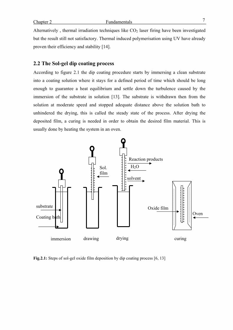
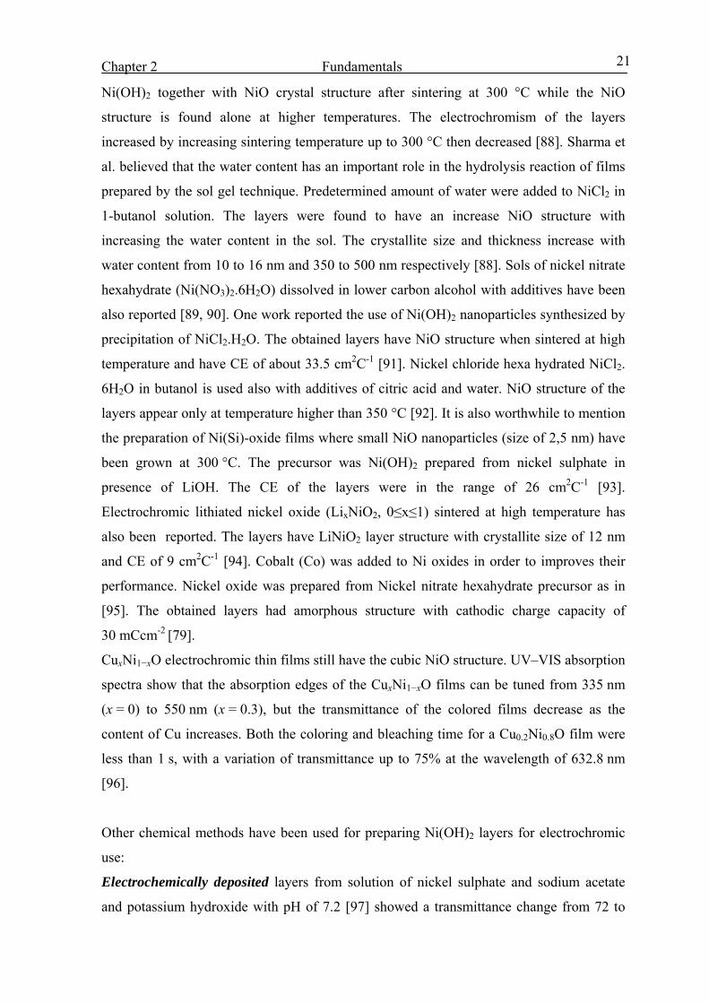
2.2 The Sol-gel dip coating process According to figure 2.1 the dip coating procedure starts by immersing a clean substrate
into a coating solution where it stays for a defined period of time which should be long
enough to guarantee a heat equilibrium and settle down the turbulence caused by the
immersion of the substrate in solution [13]. The substrate is withdrawn then from the
solution at moderate speed and stopped adequate distance above the solution bath to
unhindered the drying, this is called the steady state of the process. After drying the
deposited film, a curing is needed in order to obtain the desired film material. This is
usually done by heating the system in an oven.
Fig.2.1: Steps of sol-gel oxide film deposition by dip coating process [6, 13]
Coating bath
Sol. film
substrate
Reaction productsH2O
solvent
Oxide film Oven
immersion drawing drying curing
Chapter 2 Fundamentals
8
Principals
According to [11] the whole dip coating process can be divided to five stages: Immersion,
start-up, deposition, draining and evaporation.
The process starts with the immersion of the substrate in the coating liquid, on the
withdrawal of the substrate, it entrains liquid in a fluid mechanical boundary layer carrying
some of the liquid toward the deposition region. A streamline splits the boundary layer in
two layers: the inner layer which moves upward with the substrate and the outer layer
which moves downward to return to solution container. The thickness of the obtained layer
depends on the position of the streamline which is controlled by six forces [11]
1. viscous drag upward on the liquid by the moving substrate
2. force of gravity
3. resultant force of surface tension in the concavely curved meniscus
4. inertial force of the boundary layer liquid arriving at the deposition region
5. surface tension gradient
6. the disjoining or conjoining pressure.
The final film thickness (h), for a pure liquid with viscosity η and density ρ drawn with a
speed U, which balance the viscous drag (αηU/h) and gravity force (ρgh) is given by the
Landau- Levich equation [11]
H = 0.94 ( )
( )g
U
ργ
η
61 2
1
32
(2.4)
The exponent of U is dependent on the chemical composition of the coating solution.
The chemical formation of the coating starts when the solvents evaporate, increasing the
concentration of the solution on the substrate, the water diffuses from the atmospheres into
the layer where hydrolysis and polycondensation keep going on. Correspondingly the
viscosity of the solution in the film increases. The polymer growth during the deposition
stage may happen in a way similar to a cluster-cluster aggregation [11] with a trajectory
ranging from Brownian (in the beginning) to ballistic (at the later part of this stage).
Gelation occurs when the layer withstands the flow due to gravity but is still filled with
solvents.
The fluid flow during evaporation process accompanied by the attachment of the precursor
species to the substrate results in shear stress in the layer, while continuing shrinkage
during the drying process causes a tensile stress. The stress in the film is approximately
equal to the tension in liquid. Therefore as the film becomes rigid the tension in the film
Chapter 2 Fundamentals
9
becomes equal to the capillary stress which would shatter a macroscopic gel. However it is
found experimentally that this does not necessarily crack the films but films thicker than
1 µm usually crack.
To get a compact smooth morphology, the sol-gel coatings need heat treatment, which
could be at low temperature < 200 °C (for drying), at high temperature > 500 °C (for
sintering), or using IR or UV treatment. The heat treatment decreases the film thickness
due to the evaporation of the solvents (80 - 250 °C) followed by a consumption of the
organics (250 - 300 °C) and a reduction in the porosity of the layers [15].
2.3 Electrochromic concepts Chromism is a reversible change in a substance's colour resulting from a process caused
by some form of stimulus [16]. In most cases, chromism is based on a change in the
electron states [17] of molecules, especially the π- or d-electron state, so this phenomenon
can be induced by various external stimuli which can alter the electron density of
substances.
Electrochromism is the reversible and visible change in transmittance and/or reflectance
that is associated with an electrochemically induced oxidation–reduction reaction. It results
from the generation of electronic absorption bands in the visible region, by switching
between redox states [18].
An electrochromic material is a material that changes color in a persistent but reversible
manner by an electrochemical reaction. These materials can exhibit different oxidation
states, the color resulting from the electron delocalization between these states [3].
A generalised form of the electrochromic reaction may be written as
+Ooxidized
ne- Rreduced
(2.5)
where an electrode acts as the source or sink of electron(s), e– [17, 19].
Electrochromism is known in a number of organic and inorganic substances. Almost all of
the interesting inorganic materials are oxides and found to belong to the transition series of
the periodic table [20]. This indicates that the electrochromism has a strong relation with
the electronic structure of the materials [20].
Electrochromic materials fall in two main categories depending on the electron transfer
process which results in the coloration, namely they are anodic and cathodic materials.
Cathodic materials colour when they are reduced at a negative electrode while anodic
Chapter 2 Fundamentals
10
materials are colored at an anode [19]. Ti, Nb, Mo, Ta and W (typically group VI-B)
oxides exhibit cathodic electrochromism while Ce, Mn, Fe, Co Ir, Rb and Ni (group VIII)
oxides exhibit an anodic electrochromism. Vanadium is found to exhibit both anodic and
cathodic electrochromism depending on its oxidation state [21].
It is important to notice that for any electrochromic material to be able to exhibit
electrochromism, it should be integrated in a system where potential application is possible
[20].
The Coloration Efficiency is an important property to compare the efficiency of
electrochromic layers. It is also called electrochromic efficiency and has the units cm2C-1.
It is defined as
qODCE )()( ληλ Δ
== (2.6)
where ΔOD(λ) represents the change in optical density at the wavelength λ, resulting from
(q) charge transferred per cm2. The Optical density (OD) is an expression of the optical
transmittance of an element at a given wavelength and is expressed as log10 (1/T) where T
is the transmittance.
2.4 Electrochemical cells All electrochromic systems can be represented in principle as electrochemical cells [19] so
it is worthwhile to explain the principals of electrochemical cells. Electrochemical methods
are divided into two main methods:
Static electrochemical method: no current passes between the electrodes, concentration of
species in electrochemical cell remains unchanged
Dynamic electrochemical method: a current flows and concentrations change as a result of
a redox reaction
An electrochemical cell is composed of two compartments or half-cells, each composed of
an electrode dipped in an electrolyte solution. These half-cells are designed to contain the
oxidation and reduction halves-reactions separately where in each a certain chemical exists
in two charge states namely a reduced (R) and an oxidized (O) states which are called a
redox couple. If the potential of this redox couple is different from the equilibrium
potential then either the oxidation will occur as follows.
R → O + ne- (2.7)
or the reduction reaction in the reverse direction.

Chapter 2 Fundamentals
11
The simplest example of an electrochemical cell is shown in fig.2.2
Fig. 2.2: Schematic representation of a simple electrochemical cell [22]
The half-cell called the anode is the site at which the oxidation of zinc occurs as shown
below.
Zn (s) → Zn+2 (aq) + 2e- (2.8)
During the oxidation of zinc, the zinc electrode will slowly dissolve to produce zinc ions
(Zn+2), which enter into the solution containing Zn+2 (aq) and SO4-2 (aq) ions.
The half-cell called the cathode is the site at which the reduction of copper occurs as
shown below.
Cu+2 (aq) + 2e- -------> Cu (s) (2.9)
When the reduction of copper ions (Cu+2) occurs, copper atoms accumulate on the surface
of the solid copper electrode. As a result an immbalance of electrical charge would occur,
the anode would become more positive as zinc cations are produced, and the cathode
would become more negative as copper cations are removed from solution. This problem
can be solved by using a "salt bridge" connecting the two cells as shown in the fig 2.2.
A salt bridge is a porous barrier which prevents the spontaneous mixing of the aqueous
solutions in each compartment, but allows the migration of ions in both directions to
maintain electrical neutrality.
The electrode potential of any half cell is related to the concentration of the redox couple
according to Nernst equation:
Chapter 2 Fundamentals
12
)][][ln(0
RO
nFRTEE += (2.10)
where the square brackets denote concentrations, R is the ideal gas constant, F the Faraday
constant, T the thermodynamic temperature and n the number of electrons involved in the
reaction. E0 is the standard electrode potential.
It is important to recall that it is impossible to measure the electrode potential
independently, but the difference in electric potential is only measurable. The Ecell is
defined as the potential difference to be applied to the cell to prevent any reaction (zero
current).
Ecell = E cathode – E anode (2.11)
Electrochemists concentrate on the reactions at one electrode only which is called the
working electrode. In order to establish a scale for measuring the working electrode
potential, notation of reference electrode is introduced. The purpose of the reference
electrode is to complete the measuring circuit and provide a stable and reproducible
potential against which the working electrode is compared. The contact is made through a
liquid junction that allows the electrolyte to contact the sample. The reference electrode is
designed to produce the same potential no matter in what solution it is placed. The most
famous reference electrode is the standard hydrogen electrode (SHE) also called normal
hydrogen electrode (NHE), Pt|H2(g)(1atm), H+ (unit concentration)
It is assigned an electrode potential E = 0 at all temperatures.
One of the most common reference electrodes is the KCl saturated calomel half cell (SCE).
A simple form of this electrode can be assembled by adding in a tube, mercury metal, a
small amount of solid mercury (II) chloride, several grams of solid KCl and some distilled
water. Connection to the external measuring circuit can be made by using a fine platinum
wire dipping into the mercury pool. The potential of the SCE is 0.244 V with respect to
NHE. The principal disadvantage of the SCE as a reference is that the solubility of KCl
changes substantially with temperature and therefore the cell potential has a relatively large
temperature coefficient.
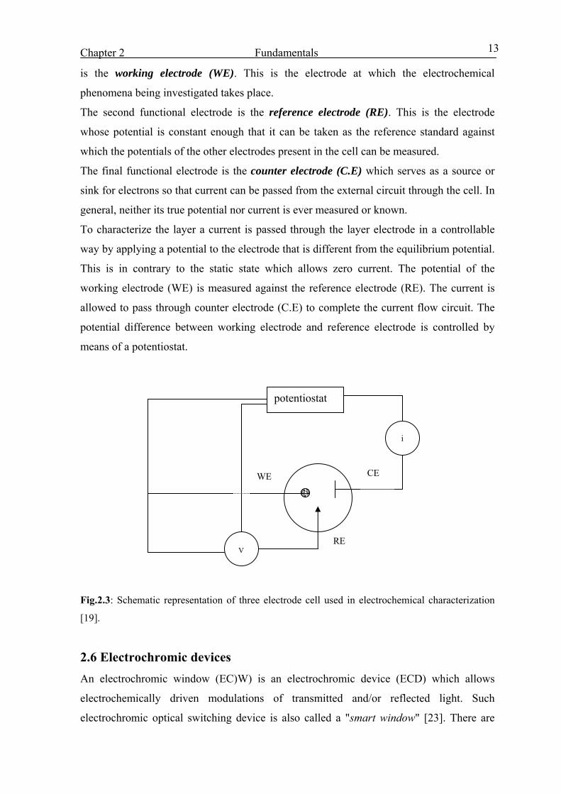
2.5 Three electrode cell Electrochromic materials are generally first studied as a single electrode under
potentiostatic or galvanostatic control. Generally, a cell used for electrochromic
measurements has three functional electrodes (see fig. 2.3). The first of the three electrodes
Chapter 2 Fundamentals
13
is the working electrode (WE). This is the electrode at which the electrochemical
phenomena being investigated takes place.
The second functional electrode is the reference electrode (RE). This is the electrode
whose potential is constant enough that it can be taken as the reference standard against
which the potentials of the other electrodes present in the cell can be measured.
The final functional electrode is the counter electrode (C.E) which serves as a source or
sink for electrons so that current can be passed from the external circuit through the cell. In
general, neither its true potential nor current is ever measured or known.
To characterize the layer a current is passed through the layer electrode in a controllable
way by applying a potential to the electrode that is different from the equilibrium potential.
This is in contrary to the static state which allows zero current. The potential of the
working electrode (WE) is measured against the reference electrode (RE). The current is
allowed to pass through counter electrode (C.E) to complete the current flow circuit. The
potential difference between working electrode and reference electrode is controlled by
means of a potentiostat.
Fig.2.3: Schematic representation of three electrode cell used in electrochemical characterization
[19].
2.6 Electrochromic devices An electrochromic window (EC)W) is an electrochromic device (ECD) which allows
electrochemically driven modulations of transmitted and/or reflected light. Such
electrochromic optical switching device is also called a "smart window" [23]. There are
V
i
potentiostat
RE
CE WE
Chapter 2 Fundamentals
14
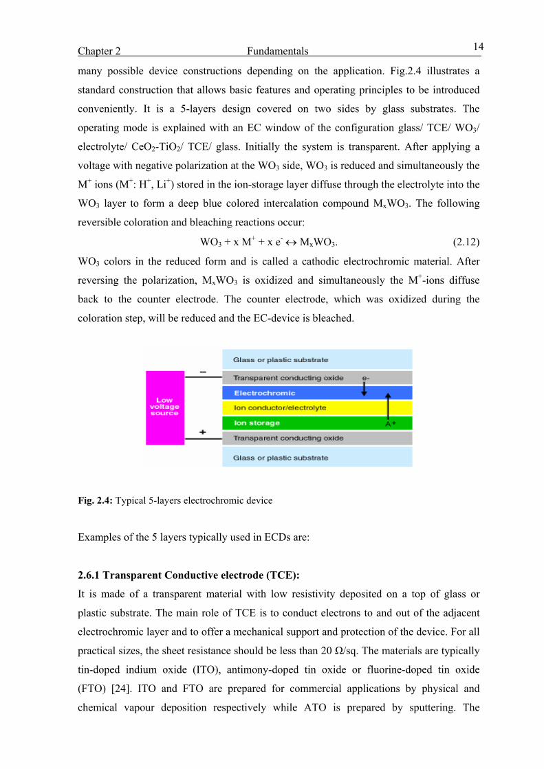
many possible device constructions depending on the application. Fig.2.4 illustrates a
standard construction that allows basic features and operating principles to be introduced
conveniently. It is a 5-layers design covered on two sides by glass substrates. The
operating mode is explained with an EC window of the configuration glass/ TCE/ WO3/
electrolyte/ CeO2-TiO2/ TCE/ glass. Initially the system is transparent. After applying a
voltage with negative polarization at the WO3 side, WO3 is reduced and simultaneously the
M+ ions (M+: H+, Li+) stored in the ion-storage layer diffuse through the electrolyte into the
WO3 layer to form a deep blue colored intercalation compound MxWO3. The following
reversible coloration and bleaching reactions occur:
WO3 + x M+ + x e- ↔ MxWO3. (2.12)
WO3 colors in the reduced form and is called a cathodic electrochromic material. After
reversing the polarization, MxWO3 is oxidized and simultaneously the M+-ions diffuse
back to the counter electrode. The counter electrode, which was oxidized during the
coloration step, will be reduced and the EC-device is bleached.
Fig. 2.4: Typical 5-layers electrochromic device
Examples of the 5 layers typically used in ECDs are:
2.6.1 Transparent Conductive electrode (TCE):
It is made of a transparent material with low resistivity deposited on a top of glass or
plastic substrate. The main role of TCE is to conduct electrons to and out of the adjacent
electrochromic layer and to offer a mechanical support and protection of the device. For all
practical sizes, the sheet resistance should be less than 20 Ω/sq. The materials are typically
tin-doped indium oxide (ITO), antimony-doped tin oxide or fluorine-doped tin oxide
(FTO) [24]. ITO and FTO are prepared for commercial applications by physical and
chemical vapour deposition respectively while ATO is prepared by sputtering. The

Chapter 2 Fundamentals
15
electrical properties of sol-gel deposited ITO are not good enough for practical uses [24].
FTO is the least expensive TCE. The FTO layers are essentially fabricated by spray
pyrolysis on float glass at 550 °C, so that their sheet resistance remains stable up to 550 °C
giving a superiority on ITO for applications which need a temperature treatment higher
than 300 °C. It is reported also that it is electrochemically more stable than ITO [25]. It
should be mentioned here that other TCEs are mentioned in the literature, such as
aluminium-doped zinc oxide and fluorine-doped zinc oxide [26].
2.6.2 The electrochromic (EC) layer.
This is typically a transition metal oxide that can exhibit several valence states upon
reduction. There are many requirements for the electrochromic layer.
• The optical modulation should be high enough to be recognized by a normal vision
observer,
• The response time should be fast,
• The ionic and electronic conductivity should be high,
• The structure should be permeable to allow an easy ion (H+, Li-) insertion
Several materials are reported for being used as electrochromic cathodically colouring
layers:
1) Tungsten oxide, WO3 is the most widely studied electrochromic layer. This is because
of its superior EC properties and relative ease of deposition by sputtering, evaporation,
chemical vapour deposition and sol-gel. The optical properties of WO3 change upon
reduction and depend strongly on the structure of the layer. Polycrystalline tungsten oxide
modulates the optical transmittance by reflection (especially in the near infrared region)
whereas amorphous tungsten oxide does that by absorption [27, 28]. Its colour changes
from transparent or yellow to deep blue due to the formation of a tungsten bronze. For
energy-efficient EC materials tungsten oxide with reflection modulation are preferred. The
proposed reaction for electrochromism in W oxide is represented in a simple form as in
equation (2.12) above.
This is an oversimplified reaction where all the details are ignored. For instance thin films
of practical interest are normally hydrated i.e., contain hydroxyl groups and water
molecules and may deviate to some extent from the stated WO3 stoichiometry in the last
equation [29].
As the size of the intercalated ions increases, the rate of diffusion decreases, thereby
decreasing the rate of optical modulation [30]. The diffusion coefficient is affected
Chapter 2 Fundamentals
16
strongly by the structure of the layers. Nagai et al. [31] reported that the diffusion
coefficient of Li+ increased from 3x10-12 to 1.5x10⁻⁹ cm2S-1 by decreasing the layer density
from 5.84 to 3.38 g/cm3.
Electrochromic films of W oxide can be prepared by a variety of techniques [32, 33], such
as evaporation [34], sputtering [35], chemical vapor deposition [36], spray deposition [37]
and sol-gel [38]. The properties of the layer depends strongly on the preparation condition
[20]. Granqvist reported in detail the techniques used in electrochromic W oxide
preparation [29].
i. Evaporation has been used successfully to produce WO3 layer for commercial EC
products such as automotive mirrors. The as-deposited films are heavily disordered with a
porosity dependent on the presence of gas. In particular, evaporation in the presence of
5×10⁻⁴ Torr of H2O yields a relative density of 0.6, whereas the deposition in a good
vacuum produces films with a relative density of 0.8 [39]. As seen by infrared
spectroscopy [40, 41] evaporated electrochromic W oxide films tend to be hydrated even if
they are produced without intentionally adding water to the deposition unit. The porous W
oxide films can be crystallized by heating. A monoclinic WO3 films were obtained by
deposition onto a substrate at 200 °C followed by a post-deposition anneal at 430°C in O2
[42]. A triclinic crystalline structure was obtained by annealing at 400°C, 500°C, and
600°C [43].
ii. DC and RF sputtering are suitable techniques for preparing electrochromic W oxide
layers with good properties. The parameters of the sputtering process have a significant
effect on the obtained layer properties [29]. Films of relative density of 0.75 and O/W ratio
of 3.1± 0.1 have been reported [44]. The substrate temperature has a strong effect on the
degree of crystallinity of the layer and it is reported that the crystallization of the films
takes place at temperatures between 300 °C and 350 °C [45-47]. There is a strong relation
between the thickness of the layer and its crystal structure [48]. Detailed study of the
structure of layers prepared by RF sputtering is given by Nabba [49]. The addition of Ti to
the W oxide improved the electrochromic properties such as the bleached state
transmittance, the colour stability and the aging durability [50].
iii. Chemical vapour deposition on the glass float line for large area electrochromic
applications might have a cost advantage in that they do not require large expensive
vacuum controlled deposition chambers. Amorphous electrochromic layers with O/W ratio
in the 2.7–3.2 range were prepared by low-temperature atmospheric-pressure chemical

Chapter 2 Fundamentals
17
vapor deposition route. The films were deposited at 100–350 °C from tungsten alkoxide
complexes [51].
iv. Sol-gel technique offers an opportunity to control the particle size and microstructure of
the layer, beside the low cost. Several precursor solutions have been used to obtain
electrochromic tungsten oxide films of the desired stoichiometry, thickness and cosmetic
quality. The precursors were based on tungsten alkoxides [52], chloralkoxides [53, 54],
colloidal solutions of tungstic acid obtained by an ion exchange method [32], and
peroxopolytungstic acid [53, 55].
For large area application the alkoxide route is not a popular choice due to high cost of
materials. The thickness of the layers obtained using a hexaethoxide precursor was in the
range of 50 nm which is not enough to get a high contrast for electrochromic application.
To get thicker layer, multi coatings are used which results in cracked layers [36].
Hydrolysis of tungsten alkoxide of the two components WO(OEt)4 and WO2(OEt)2 has
been studied. The hydrolysis products and the partially hydrolyzed solutions have been
characterized by means of X-ray diffraction, IR, electron spectroscopy and small-angle X-
ray scattering. The obtained tungsten solutions have been described as typical polymeric
sols. Sols were used for the preparation of electrochromic and photochromic films by spin-
coating techniques [56]. An alternative low cost method is to use chloroalkoxide precursor
which resulted from reacting tungsten chloride with alcohol The resulting material is
diluted with more alcohol to obtain the solution [57-59]. Films with nanocrystals of
tungsten oxide are embedded in an amorphous matrix and Hydrous phases WO3
(WO3 · nH2O) are also present. These features improve the electrochromic properties
allowing high charge transfer during the electrochromic process, fast optical switching and
stability of the optical state. Layers heated at temperature higher than 300 °C are less
efficient with respect to those annealed at lower temperatures [59].
The peroxo route starts with tungsten metal and reacting it with excess hydrogen peroxide
(or its mixture with an organic acid) under controlled conditions of temperature, resulting
in a precursor with enhanced stability [60-63]. It offers the advantage of the formation of
pristine metal oxide films at a relatively low temperature owing to the clean burn out
properties of organic additives (with low carbon content) and other volatiles from the as-
deposited film Further improvements in the properties are possible by chemical
modification of the precursor material and by controlling the post deposition thermal
treatment [64]. Modifying the precursor solution chemistry by adding 0 to 5 wt.% of oxalic

Chapter 2 Fundamentals
18
acid dihydrate modifies the microstructure of the films. The film obtained from a sol with
3 wt.% oxalic acid dihydrate, showed a coloration efficiency of 102 C cm−2 (at 800 nm),
fast color–bleach kinetics (tc of about 192 s and tb of about 28 s) and an ion storage
capacity of 18.6 mC cm−2 [62]
One of the advantages of the sol gel method is the control of the microstructure of the
layer by introducing chemical dopants to the reactant sols. Different amounts of Titanium
precursor was mixed with tungsten precursor (1, 5, 10 and 15 mol %). Although, the
coloration efficiency decreases when the titania content is increased, the electrochromic
properties of the WO3–TiO2 films heat treated at a relatively high temperature were
improved due to the amorphous structure preserved by the Ti-addition. Even small
additions of titania can produce significant structural changes of tungsten oxide films [58].
The electrochemical responses of amorphous thin films of lithium doped tungsten trioxide
(LixWO3) prepared by the sol gel method (by reacting metallic tungsten with hydrogen
peroxide (30%) and acetic acid) were studied by quartz crystal microbalance technique. It
was observed that the coloration mechanism is the same for the pure and the doped films.
However, the kinetics of the processes are different for the undoped and doped films.
These differences are in agreement with the electrochemical properties presented by these
films. In the pure WO3 films, in which the deintercalation processes are more difficult, the
kinetics of the coloration process is slower. In other words, the undoped films visibly
return to the original color more slowly than the doped films does [65].
Electrochromic W-Mo oxide films were fabricated by adding different percentages of
molybdenum to tungsten oxide ranging from 0.5 wt % to 7 wt% of deposition solution.
Normal optical transmittance was also measured and it was found that coloration occurs in
a shorter time than the bleaching. The time constant of the process tends to increase with
the molybdenum oxide doping concentration [66].
Although a hexagonal-like structure is obtained by different deposition techniques, a
tetragonal structure has been reported for layers obtained by adding ethylene glycol to
tungsten precursor [67] and annealed at a temperature of 500 °C.
The color of tungsten trioxide changes from transparent to deep blue upon reduction. This
blue color can be changed through the addition of other oxides or metals. In the case of
V2O5 addition, the reduced film is green, and when gold particles are added to a cermet of
tungsten oxide, the reduced material was red.
.
Chapter 2 Fundamentals
19
2) Niobium oxide, Nb2O5, is reported to have EC properties comparable to those of WO3,
although the use of this material has been limited as a cathodic EC film in a patented
device. The suggested reaction is
Nb2O5 + 2H+ + 2e- ↔ Nb2O3(OH)2 or 2Nb2O2.H2O (2.13)
It can be deposited by many methods including sputtering [68, 69], chemical vapor
deposition [70] and wet chemical routes [71]. Nb(OR)5 alkoxides are quite expensive and
highly sensitive to moisture so that sol-gel routes are based mainly on chloroalkoxides [71,
72]. The color of the reduced layer depend on the crystallization degree: the amorphous
layer turns to a gray brown color upon reduction, the crystallized turns to dark blue [24].
Lithiation of Nb2O5 through the addition of a lithium salt to the precursor solution
enhances the EC kinetics in particular the bleach rate and the reversibility for lithium
intercalation. This was shown for both the amorphous and crystalline material [73]. In
comparison to WO3, niobium oxide requires higher potentials for color and bleach and has
slower EC kinetics. Coatings of pure and Zr, Sn, Li, Ti and Mo doped niobium pentoxide
have been prepared by the sol–gel process and deposited on ITO-coated glass using the dip
coating technique. The coatings were transparent and, depending on the nature and amount
of the doping and the sintering temperature, they presented a brown, gray or blue color
after Li+ insertion [74]. Nb2O5 films containing TiO2 between 0.05 and 0.5 mol% showed
an increase in ΔT and CE compared to undoped layers and presented ΔT= 84% and
CE=26.9 cm2 C−1. Above this concentration, the ΔT and CE values decreased [75].
Many other TMOs thin film are electrochromic, e.g. the oxide of Molybdenum MoO3,
[76, 77] where both amorphous and polycrystalline MoO3 show an electrochromic effect
similar to WO3 and vanadium V2O5 which is reported to have cathodic and anodic
electrochromic properties. Electrochromic layers of mixed oxides have been also reported.
2.6.3 Counter electrodes or Ion Storage layer
The counter-electrode should offer a high transmittance in the visible range, with fast
kinetics for the electrochemical reaction, and should have a sufficiently high charge
capacity for the insertion/extraction of ions. There are two choices for the counter-
electrodes: they can be optically passive, i.e. their transmittance remains unchanged during
the ion intercalation /de-intercalation process to avoid interference with the electrochromic
layer coloration and they are called ion storage layer (IS), or they may exhibit
Chapter 2 Fundamentals
20
colouration/bleaching properties in complementary way with the electrochromic layer. In
the later case the device has a cathodic EC layer and an anodic EC counter electrode so
that both coatings colour and bleach at the same time.
a) Anodically coloring counter electrodes
1) Nickel oxide, NiO, is one of the most widely studied materials. NiO has been used in an
all-solid state thin film devices involving the insertion of both protons and hydroxyl groups
[78]. The NiO films are colorless in the reduced state and become dark brown when
oxidized. Beside being used as counter electrode with cathodically coloring layer it could
be used also as working EC layer with passive counter electrode as it will be explained in
this work.
Many techniques are available for preparing electrochromic NiO thin films. The major
methods are categorized into physical, chemical and electrochemical ones. For the
different deposition techniques the layers have molecular species primary built with NiO6
blocks and it is regarded as a cluster-assembled material [20].
i. Chemical methods
Vacuum techniques, typically evaporation and sputtering need vacuum which makes them
expensive methods. Wet chemical deposition is an alternative method for producing
amorphous thin films with high surface area [79]. The problem faces this method is the
lack of soluble nickel alkoxide.
Sol-gel: NiO films have been prepared using sols of different precursors. In the beginning
sol-gel routes went into two main ways, using either sulphate or nitrate precursor but later
other precursors like nickel chloride and nickel acetate have been used. Aqueous sols of
Ni(OH)2 have been obtained by precipitating NiSO4 in presence of LiOH and acetic acid.
NiO with grain size of about 2-3 nm was detected by TEM. Change in transmittance in the
range of 40-60 % and 35-40 mC/cm2 charge capacity are reported [80-83]. The same sol
was prepared by alternate immersion in NiSO4 and KOH solutions [84]. Sols of nickel
diacetate tetrahydrate (Ni(CH3COO)2.4H2O) dissolved in pure methanol [85] or in dry
dimethylaminoethanol (dmaeth) [86, 87] or of nickel diacetate dmaeth
(Ni(acetate)2(dmaeth)) in dry dimethyaminoethanol have been used. The layers have an
amorphous structure. The coloration efficiency varied between 6.2 and 16.4 cm2/C
according to the concentration of the sol and the thickness of the layer [86]. Layers
prepared with sols of nickel chloride (NiCl2) in different solvents are found to consist of
Chapter 2 Fundamentals
21
Ni(OH)2 together with NiO crystal structure after sintering at 300 °C while the NiO
structure is found alone at higher temperatures. The electrochromism of the layers
increased by increasing sintering temperature up to 300 °C then decreased [88]. Sharma et
al. believed that the water content has an important role in the hydrolysis reaction of films
prepared by the sol gel technique. Predetermined amount of water were added to NiCl2 in
1-butanol solution. The layers were found to have an increase NiO structure with
increasing the water content in the sol. The crystallite size and thickness increase with
water content from 10 to 16 nm and 350 to 500 nm respectively [88]. Sols of nickel nitrate
hexahydrate (Ni(NO3)2.6H2O) dissolved in lower carbon alcohol with additives have been
also reported [89, 90]. One work reported the use of Ni(OH)2 nanoparticles synthesized by
precipitation of NiCl2.H2O. The obtained layers have NiO structure when sintered at high
temperature and have CE of about 33.5 cm2C-1 [91]. Nickel chloride hexa hydrated NiCl2.
6H2O in butanol is used also with additives of citric acid and water. NiO structure of the
layers appear only at temperature higher than 350 °C [92]. It is also worthwhile to mention
the preparation of Ni(Si)-oxide films where small NiO nanoparticles (size of 2,5 nm) have
been grown at 300 °C. The precursor was Ni(OH)2 prepared from nickel sulphate in
presence of LiOH. The CE of the layers were in the range of 26 cm2C-1 [93].
Electrochromic lithiated nickel oxide (LixNiO2, 0≤x≤1) sintered at high temperature has
also been reported. The layers have LiNiO2 layer structure with crystallite size of 12 nm
and CE of 9 cm2C-1 [94]. Cobalt (Co) was added to Ni oxides in order to improves their
performance. Nickel oxide was prepared from Nickel nitrate hexahydrate precursor as in
[95]. The obtained layers had amorphous structure with cathodic charge capacity of
30 mCcm-2 [79].
CuxNi1−xO electrochromic thin films still have the cubic NiO structure. UV–VIS absorption
spectra show that the absorption edges of the CuxNi1−xO films can be tuned from 335 nm
(x = 0) to 550 nm (x = 0.3), but the transmittance of the colored films decrease as the
content of Cu increases. Both the coloring and bleaching time for a Cu0.2Ni0.8O film were
less than 1 s, with a variation of transmittance up to 75% at the wavelength of 632.8 nm
[96].
Other chemical methods have been used for preparing Ni(OH)2 layers for electrochromic
use:
Electrochemically deposited layers from solution of nickel sulphate and sodium acetate
and potassium hydroxide with pH of 7.2 [97] showed a transmittance change from 72 to
Chapter 2 Fundamentals
22
33 % and response time from 20 to 40 s. The ones which deposited from 0.01 M Ni(NO3)2
solution with different proportions of Mn(NO3)2 varied from 0 to 100 % showed a shift in
Ni(II)/Ni(III) redox reaction to less positive potentials. The solution which showed a good
result related to the stability was that with 95 % Ni(OH)2 and 5 % Mn(OH)2.[98]. NiOx
thin films were deposited on sol-gel ITO coated glass using triangular waveform between
-0.5 to 1.5 V from solution of 0.1 NiSO4 and 0.1 M NH4OH [99]. The layers were tested in
both LiClO4 and KOH solutions. Ni(OH)2 layers were cathodically deposited from solution
of Ni(NO3)2 [100] or anodically in order to improve the stability of the obtained layer.
Layer deposited by Alternative dipping deposition (ADD) using solutions of NiSO4 and
KOH exhibited CE of 35 cm2C-1 [84] and those using solution of NiSO4 with NaOH had
CE of about 70 cm2C-1 [101],
Chemical Bath Deposition (CBD) and Liquid Bath Deposition (LBD) techniques have
been also used to prepare NiO layers using cold ammonia complex solution of NiSO4 and
Na2S solutions [98] and mixed solution of saturated NiF2 and H3BO3 [101]respectively.
ii. Physical Techniques
Sputtering is considered as the most common physical techniques used for thin films
depositions. Preparing electrochromic Nickel oxide thin films by rf reactive magnetron
sputtering started in 1986 [102]. Later DC reactive magnetron sputtering techniques have
been also used [103-109]. In general the reported layers have a polycrystalline NiO
structure with (111) preferred orientation [110], while the grain size varies widely with the
deposition conditions from 3 to 150 nm [111].
One of the consistent problems of sputtered NiO layers is the residual coloration of the
bleached state. Different additives have been tried to improve the transmittance of the layer
in the as-deposited and bleached states such as (Cr, Al, V and Mg oxides) [105-108]. Cr
oxide is found to decrease the transmittance change while the charge capacity is not
affected. The structure is found to consists of NiO crystals impeded in amorphous structure
of CrO with a grain size of 10 nm [105]. In general Al and Mg oxides additives increase
significantly the luminance transmittance of the layers in the bleached states while the
charge capacity is maintained [112].
In general, the life time of electrochromic sputtered NiO films (2x10⁴ cycles) [102] is
higher than that of the layers prepared by the other techniques.
Chapter 2 Fundamentals
23
The effect of oxygen flow in sputtering chamber was tested by changing the gas mixture
of Ar and O2 from 5% to 30% maintaining the other parameters constant [103]. It was
found to have a strong effect on the charge capacity of NiO layers sputtered from NiO
target that decreases from 4.9x10⁻² mC/cm2 nm1 with a 5 % O2 flow to
1.9x10⁻² mC/cm2nm1 at 30%. The lowest detected Ni/O ratio by RBS was 0.5. The O2 flow
did not have the same strong effect with samples sputtered from a Ni target while the Ni/O
ratio increased from .9 to 1.5 by increasing O2 flow [103].
Another study by Avendano et al. [107] performed on mixed NiV oxide layers showed that
by increasing the O2 content in the sputtering gas from 0.4 to 6.4%, the layer evolved from
a metallic to a transparent to brown. The O/Ni ratio as determined by RBS increased from
0.63 (.8% O2) to 1.85 at 2 % O2. The electrochromic characteristics of the layers were also
found strongly dependent on the O2 content of the sputtering gas, an intermediate content
only giving rise to significant transmittance change and charge capacity. The optimum
performance was found at an oxygen concentration smaller than 1.5 %. Layers deposited at
low oxygen level did not exhibit any electrochromic effect while high O2 level leads to a
deterioration of the optical modulation.
While an excess of O2 in the gas mixture lowers the transmittance of the as-deposited
films, H gas addition produces transparent layers with better crystallinity [113] and
improves the electrochromic effect [113-115]. On the other hand Azen et al. [116] found
no differences between devices using nickel oxide layers deposited in the presence or
absence of H.
Electrochromic lithium nickel oxide thin films are made by rf sputtering from LiNiO2
target [117]. They had a coloration efficiency between 40 and 50 cm2C-1and a
transmittance change of about 70 %.
The effect of rf power on the structure of non stoichiometric NiOx films sputtered from
metallic nickel target was investigated [110] and it was found that the lattice parameter
decreases by increasing the rf. power. Oxygen to nickel ratio higher than one was detected
with huge ratio of hydrogen to nickel. The maximum transmittance change (52 %) was
detected for rf power of 150 W.
The role of defects on the electrochromic response time of sputtered Ni oxide films was
tested by Ahn et al. [118] where it was found that the excess interstitial oxygen and voids
disturb the proton intercalation/deintercalation process. Wu et al. [119] found that the ion
transport behavior during the electrochromic process is so complex and dependent on the
Chapter 2 Fundamentals
24
layer deposition and testing conditions where the change of oxygen and nickel vacancies is
suggested to be responsible for such behavior.
Electron beam evaporation: Layers were prepared by electron beam evaporation showed a
NiO structure [120-123] with (111) preferable orientation [121].
The effect of substrate temperature on the electrochromic properties of NiO layers
deposited by electron beam evaporation from pellet of NiO powder was investigated by
changing the substrate temperature between 80 and 250 °C. The transmittance of the as-
deposited state remains within the same range (70 %) for temperature between 80- 200 °C
while layers deposited on substrate maintained at 250 °C have a slight blue color and lower
transmittance value. This was explained as due to a change in the composition of the layer
due to the lack of oxygen or due to the decomposition of the NiO at high temperature. The
absorption edge also is shifted with increasing substrate temperature which means a
decrease in the band gap. The poor electrochromic effect of layers deposited at high
temperatures was attributed to the compact granular structure of the with large grain size
and small grain boundaries. Durability tests were also performed with layers deposited on
substrates at different temperatures and the results showed that 150 °C was the optimum
temperature with a change in optical density of 0.88 and a cathodic charge capacity of
about 18.1 cm2C-1 [120].
The effect of the deposition pressure on the microstructures and electrochromic properties
of NiO layers deposited by electron beam evaporation was tested by Agawal et al.[122].
The layers were found to have a NiO microcrystalline cubic structure regardless of the
deposition pressure, but by increasing the pressure in the chamber from 6.7x10⁻² to
2.7x10⁻⁴ Pa. The porosity of the films increases due to the decrease of the grain size from
6.7 to 4 nm. The calculated O/Ni ratio increased from 1.17 to 1.25. The coloration
efficiency decreased by increasing the pressure from 40 to 32.5 cm2C-1.
The interesting conclusion of this report is that the authors believe that the active site in
NiO films are in the bulk and not at the surface of the film where they found that large
surface leads to poor electrochromic effect. The hydration of the surface and the
intercrystalline OH- are important for high ionic (hdroxyl ion) conductivity.
The Pulsed laser deposition technique was used also to produce electrochromic NiO
layers [124-126] and lithiated Nickel oxide [127]. The layers were polycrystalline with the
cubic NiO structure. Cobalt and tantalum have been added to enhance the electrochromic
Chapter 2 Fundamentals
25
performances of nickel-based oxide thin films. Among the two series of metal additions
(M ≤ 20%), the Ni–Co–O (5% Co) and Ni–Ta–O (10 % Ta) thin films showed the highest
electrochemical performances and especially an improved durability [128]. W addition was
tried also by Penin et al. [129] and led to a progressive film amorphization. An increase in
cyclability for Ni–W–O (5 % WO3) electrode, cycled in 1 M KOH electrolyte, was
associated with a limited dissolution of the oxidized phases was achieved with tungsten
addition. HRTEM investigations of cycled films revealed that the stabilization is correlated
to the existence of an α(II)-nickelhydroxide phase.
2) Iridium oxide, IrO2, is another anodic material [130, 131]. It colours from transparent
to light brown at positive potential in Li+ based electrolytes. IrO2 was prepared by different
methods, reactive sputtering [130, 131], vacuum deposition of iridium metal [132], thermal
oxidation of vacuum-deposited iridium-carbon composite films [133] and sol gel [134].
The sol gel route is rather difficult because the synthesis of iridium alkoxide is difficult and
therefore the precursors solutions were based mainly on IrCl3.3H2O [135, 136]. The
colouration efficiency and the response time of IrO2 are comparable to WO3 [137]. An
electrochromic devices based on WO3 as electrochromic layer and IrO2 as counter
electrode was realized [138]. In spite of its good electrochromic efficiency and stability,
IrO2 is not used for practical applications because it is an extremely expensive material.
3) Vanadium pentoxide V2O5 colours anodically from nearly colourless to a bright yellow
state when oxidized. This film works best with a non-aqueous lithium ion electrolyte but
the change in coloration in the visible range is not strong enough to be used as an
electrochromic layer so it is used as an ion storage layer rather than as an electrochromic
layer. As V2O5 has a weak cathodic coloration in the red and infrared, it is not a good
electrochromic counter electrode with tungsten oxide, due to its modulation of the solar
spectrum [139]. However, mixed oxides of vanadium and chromium or niobium oxides
[140] have been reported to significantly decrease or eliminate the modulation in the near
infrared while maintaining a high charge capacity.

Chapter 2 Fundamentals
26
b) Passive counter electrodes
1) Cerium–Titanium oxide layer (CeO2-TiO2)
Between the different used counter electrodes, CeO2 which has two stable valences states
(III) and (IV), was proposed for transparent and colourless electrodes but its response time
is too low compared to those of WO3. To overcome the slow reaction kinetics in CeO2
films, Baudry et al. [141] suggested the replacement of part of the Ce atoms by an element
of lower ionic radius such as Ti. For the preparation of this new oxide thin film, they used
Ce(NH4)2 (NO3)6 and Ti(OPri)4 in ethanol as starting materials and found that the current
densities obtained for a thin film with Ce/Ti molar ratio of 1:1 are 3 times higher than that
obtained for pure CeO2 films and the diffusion coefficient of Li ions is 10 times higher. As
the electronic resistivity of TiO2 has the same order of magnitude as that of CeO2 [142,
143], the increase in current densities when Ti is added is due to the increase of Li
mobility. The work of Baudry et al. [141] was followed by series of other papers [144]
using the same precursor in ethanol, isopropanol or methoxy-ethanol.
100 nm thick CeO2-TiO2 layers with a molar ratio of Ce/Ti = 0.5 were prepared by
Avellaneda et al. [145] by the sonocatalytic sol–gel method using the same precursor in
isopropanol. The layers were calcined at 450 °C in an oxygen atmosphere. Xerogels were
characterized by thermal analysis (DTA–TG) and X-ray diffraction. The cathodic and
anodic charges during cyclic voltammetry measurements at a scan rate of 50 mV/s were
about 16 mC/cm2 and the process was fully reversible up to 4500 cycles.
Equimolar CeO2-TiO2 films were fabricated with the same precursors in a mixture of
ethanol and water and with addition of a small amount of acetic acid by Ghodsi et al.
[146]. The surface composition of the films were studied by X-ray photoelectron
spectroscopy (XPS). A scanning electron microscope was used for the analysis of the
surface structure. The optical band gaps were Egd=3.59±0.12 eV and Eg
ind=3.19±0.08 eV
for the direct and the indirect transitions, respectively independent of the dipping rate and
the number of layers.
Optical indices of CeO2-TiO2 films have been determined by Rubin et al. [147] for
stoichiometric composition prepared by both PLD and sol–gel. Measurements were made
using a combination of variable-angle spectroscopic ellipsometry and spectroradiometry.
The optical constants were then extracted using physical and spectral models. The sol–gel
films were much rougher than the PLD films and poor agreement between the surface
roughness predicted by the optical model and that derived from the AFM measurements
Chapter 2 Fundamentals
27
was found. The index of both films is however similar and they follow the classical normal
dispersion forms decreasing asymptotically towards higher wavelengths. For the PLD film,
n= 1.76 at 550 nm and for the sol–gel film a little bit higher n=1.83. The films were
slightly yellow with the fundamental absorption falling off to negligible levels around
450 nm.
Cerium chloride (CeCl3) and titanium isopropoxide Ti(i-PrO)4 were the starting materials
in the method proposed by Makishima et al. [148, 149] and used later by Stangar et al.
[150]. Ce/Ti mole ratio of one to one was used. The use of these precursors improved the
electrochemical properties of the obtained layers but not the optical ones.
Nothing was reported about the structure of the CeO2–TiO2 structure until Tonazzi et al.
[151] studied by X-ray scattering the same films prepared by Baudry et al. [141] and
proposed that small crystallites of CeO2 are included in an amorphous matrix of TiO2. No
defined compound was observed.
Later Keomany et al. [152, 153] studied the structure of CeO2-TiO2 films prepared using
other precursors e.g. by mixing two alkoxides, Ce(OBus)4 and Ti(OBun)4 and varying the
composition range between pure TiO2 and pure CeO2. The coatings were found amorphous
for concentrations of CeO2 below 50 % and the size of the CeO2 nano crystallites included
in the TiO2 amorphous matrix increases from ~1 nm for 5 % CeO2 to 5 nm for pure CeO2.
Recently Verma et al. [154] studied the structure of CeO2–TiO2 layers deposited by dip
coating from an ethanolic solution of CeCl3·7H2O (0.22 M) and Ti(OPr)4 with different
Ce/Ti compositions. The XRD investigations showed the prevalence of amorphicity in the
films constituted with 50 % or lower mole percentage of CeO2. The compositions with
higher CeO2 contents exhibited nanocrystallinity and were distinguished by the existence
of diffraction peaks assigned to cerianite and the mixed compound CeO1.6·2TiO2. In all the
compositions the presence of TiO2 in the amorphous phase was clearly evident.
The improvement obtained by adding TiO2 to the pure CeO2 layers depends on the material
preparation mode and on the nature of the electrolyte, as shown e.g. by Stangar et al. [150].
who performed cyclic voltammetric measurements in LiOH electrolyte for both pure CeO2
and mixed CeO2-TiO2 layers. The CeO2 system exhibits higher overall electrochemical
reversibility when compared to the CeO2-TiO2 system. Coulometric measurements as a
function of the coating thickness showed that CeO2 exhibits a larger storage capability. The
CeO2/LiOH system is also less sensitive with regard to the coating thickness. These

Chapter 2 Fundamentals
28
differences could be due to the presence of protons, differently adsorbed at the surface of
CeO2 and TiO2, or to a different film structure, because the films of CeO2 and CeO2-TiO2
were prepared using different cerium precursors; inorganic ((NH4)2Ce(NO3)6) precursor
which was used for the preparation of the CeO2 thin solid films while the CeO2-TiO2
coatings have been made by using mixed organic-inorganic (Ti(OiPr)4 and CeCl3·7H2O)
precursors.
There are also instances where laboratory sol–gel devices have been fabricated without an
IS film but using a suitable electrolyte [155].
2.6.4 Electrolyte
A suitable electrolyte with low electronic and high ionic conductivity is placed between the
electrochromic (EC) and ion storage layers (IS). Besides acting as an ionic conductor, the
electrolyte has also a mechanical role in supporting the device. Usually, the electrolyte
must fulfil several requirements: it must be an electronic insulator (σe<10−12 S/cm) and be a
good ionic conductor (usually 10−7<σi<10−4 S/cm). If the application requires that the
device can be switched to the transparent state, then the ionic conductor must be also
transparent and neutral colouring. The electrolyte should also not react with the two
insertion electrodes in between it is sandwiched. This chemical stability must be ensured
both during the deposition and during the cycling. Finally, for certain applications (e.g.
windows), the electrolyte must be also stable in certain temperature range and under solar
radiation [156]. In general the electrolytes used in electrochromic devices can be classified
into two main categories: liquid and solid electrolyte
A Liquid electrolyte has the advantage of having high diffusion rates for the ions. Its use is
limited to small size ECD due to the risk of leakage and dissolution of the EC and IS layer
which leads to a fast degradation of the device [24]. Inspite of that, liquids are still being
used for laboratory studies and are prepared using easily ionised salt dissolved in
appropriate solvents. The most common salts are LiClO4 and LiBF4 salts for Li ions
conduction where propylene carbonate (PC) and dimethyle florine (DMF) are used as
solvents.
A Solid electrolyte can be classified into organic and inorganic electrolyte. Organic
electrolytes fall into two main types: polymer electrolyte and polyelectrolytes. Polymers
electrolyte are macromolecules containing dissolved Li salt or acid [19] depending on the
needed ion transport. Cross-linked polyether (CPE), polyethylene oxide (PEO) and
Chapter 2 Fundamentals
29
polyvinyl alcohol (PVA) are the most common polymer matrix used in solid electrolyte
synthesis. LiClO4 and H3PO4 have been used as ion sources.
Polyelectrolytes are polymers containing ion-labile groups. Most common examples are
polyperflourosulphonic acid (Nafion) poly methyl methacrylate (polyMMA) and
polyethylene sulphonic acid (polyESA) [19].
The inorganic electrolytes are mainly oxides which serve as media for cation conduction,
such as Ta2O5 and ZrO2. It has the advantage over organic electrolytes in their enhanced
stability to photolytic degradation.
The main problem of solid electrolytes are the significant interfacial contact resistances
and their fragility. Many researchers have attempted to address these problems by using
various thickened electrolytes consisting of a major solvent system, an ionic salt, and an
intermediate molecular-weight polymer. This type of electrolyte is attractive for device
applications due to the ease of preparation and the ability to reduce many of the unwanted
effects shown by a strictly liquid electrolyte. Ideally, however, a more rigid electrolyte is
desirable. While a rigid electrolyte can be achieved with high molecular-weight polymer
additions, it can lead to great difficulty during filling and assembly of the devices by
requiring high pressure and or temperature to achieve a proper flow for rapid and uniform
assembly.
Some hybrid organic–inorganic sol–gel materials have been suggested as electrolytes in
EC devices. "Aminosils" are obtained from H2NSi(OR)3 precursors hydrolyzed in the
presence of strong mineral acids such as HClO4 or HCF3SO3 [153]. The silica backbone
provides mechanical strength while the amino groups and the acid provide the proton
conduction [157].
Sol–gel-derived and polymeric solid or semi-solid electrolytes of different kinds are now
used in experimental electrochromic devices
All gel electrochromic devices have been made using hybrid gels made from Ti(OBun)4,
acetic acid and glycerol as a proton conducting electrolyte [33].
2.7 Area of applications The motivation for all efforts to develop electrochromic materials is their potential
technical application. Few of them have already found their way to the markets such as
rear-view mirrors for cars and vehicle. Next will come the electrochromic glazing where
the main areas are automotive and architectural, with automotive being the most likely
entry point because of its smaller size although it is necessary to have a high transmittance
Chapter 2 Fundamentals
30
of the bleached state (more than 70 %), a requirement is not so critical for architectural
applications. Finally come the display devices. Some other applications are to be in use in
the future such as EC ophthalmic eyewear [3]. In general ECDs are not so common in the
markets due to lack of suitable manufacturing techniques and durability of the available
devices [158].
2.7.1 Smart window
It is one of the most important applications, which works as light and heat filters for the
external glazing of buildings leading to a reduction in fossil fuel consumption. It has the
typical structure of five layers EC device structure shown above (fig. 2.4). The primary
advantage of an EC glazing is the capability for a dynamic control of the transmittance of
the glass. In summer it is used to reject the maximum possible IR radiation to lower the air
conditioning cost while in winter it is set to pass as much as possible the IR to warm the
interior place. This has great economical benefits. One main advantage of EC glazing is the
dynamic control of the color state so it can provide nighttimes insulation and privacy and
can be also adjusted to reduce glare. A number of criteria are necessary for electrochromic
smart window applications. They are summarized as follows [159, 160]:
• continuous range in solar and optical transmittance, reflectance and absorptions
between bleached and colored states,
• contrast ratio (CR) of at least 5 : 1,
• coloring and bleaching times (switching speed) of a few minutes,
• operating glass surface temperatures of –20 °C to +80 °C,
• switching with applied voltages of 1 to 5 V,
• open circuit memory of a few hours (maintains a fixed state of transmittance
without corrective voltage pulses),
• acceptable neutral color,
• large area with excellent optical clarity,
• sustained performance over 20–30 yr,
• acceptable cost
The automotive glazing like sunroof and side windows have an advantage over the
architectural windows because of their smaller size and shorter required life time, although
the upper temperature limits are higher (90–100 °C) [158]. Table. Summarize the
important requirements for glazing used in automobile glazing (sunroof and side windows)
[24].
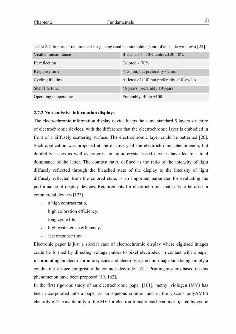
Chapter 2 Fundamentals
31
Table 2.1: Important requirement for glazing used in automobile (sunroof and side windows) [24].
Visible transmittance Bleached 41-70%, colored 20-10%
IR reflection Colored > 70%
Response time <15 min, but preferably <2 min
Cycling life time At least >2x10⁴ but preferably >105 cycles
Shelf life time >5 years, preferably 10 years
Operating temperature Preferably -40 to +100
2.7.2 Non-emissive information displays
The electrochromic information display device keeps the same standard 5 layers structure
of electrochromic devices, with the difference that the electrochromic layer is embodied in
front of a diffusely scattering surface. The electrochromic layer could be patterned [20].
Such application was proposed at the discovery of the electrochromic phenomenon, but
durability issues as well as progress in liquid-crystal-based devices have led to a total
dominance of the latter. The contrast ratio, defined as the ratio of the intensity of light
diffusely reflected through the bleached state of the display to the intensity of light
diffusely reflected from the colored state, is an important parameter for evaluating the
performance of display devices. Requirements for electrochromic materials to be used in
commercial devices [123].
- a high contrast ratio,
- high coloration efficiency,
- long cycle life,
- high write–erase efficiency,
- fast response time.
Electronic paper is just a special case of electrochromic display where digitised images
could be formed by directing voltage pulses to pixel electrodes, in contact with a paper
incorporating an electrochromic species and electrolyte, the non-image side being simply a
conducting surface comprising the counter electrode [161]. Printing systems based on this
phenomenon have been proposed [19, 162].
In the first rigorous study of an electrochromic paper [161], methyl viologen (MV) has
been incorporated into a paper as an aqueous solution and in the viscous polyAMPS
electrolyte. The availability of the MV for electron-transfer has been investigated by cyclic
Chapter 2 Fundamentals
32
voltammetry at a stationary platinum disc electrode. The brief study of the
electrochemistry of prussian blue (PB) and methyl viologen in paper was published by
Rosseinsky and Monk in 1989 [162], in which the electrochromes methyl viologen, 1-
methyl-1′-hyphoxyethylphenyl viologen and PB were separately immobilised in the paper,
the working electrode being a glassy carbon. Their conclusion was that the voltammetric
response of all three electrochromes was essentially the same in paper as that in solution,
albeit with complexities caused by iR drop and fluctuating humidity.
2.7.3 Electrochromic Mirror
This is the most mature electrochromic application and it is already available in market as
rear and side view mirrors for cars and vehicles. One modification has to be done to the
standard electrochromic device construction, and a reflecting electrically conductive back
electrode is used instead of a rear transparent conductive electrode.
During daytime viewing, the rear view mirror is set so that the electrochromic component
is in the bleached state with a reflection from the back reflecting part of the mirror. At
night, the mirror is switched on when the headlights behind the car only hit a
photosensitive sensor on the front glass surface of the mirror. Since the light has to pass
twice through an absorbing medium, the reflectivity of the system is low and the glare is
significantly reduced. The function of electrochromic mirrors was discussed intensively by
Baucke [163, 164].
2.8 State of art of electrochromic devices based on NiOx electrode Electrochromic devices behaves as rechargeable thin film batteries whose energy content
or state of oxidation is optically indicated [165].
Special attention has been devoted to designs incorporating electrochromic hydrated nickel
oxide films operating in conjunction with electrochromic tungsten oxide. This combination
of materials is favorable with regard to electrochemical potentials and also for the
possibility to attain a neutral gray color in the dark state [4]. Many glass-based devices
have been investigated.
Fundamental properties of all-solid-state electrochromic windows to control the solar
energy have been investigated using devices with configuration Glass/ITO/NiO/Inorganic
Electrolyte (Ta2O5, etc.)/ WO3/ITO/ Adhesive Film/ Glass. They modified the visible
transmittance between 72.6 % and 17.6 % and had a cyclic life over 100000 cycles at
60 °C. Based on the accelerated weathering tests, the stability of the system is estimated to
Chapter 2 Fundamentals
33
be over five years for outdoor applications. In general, the most important features of such
systems are their environmental stability and the possibility of large area applications
technology [166].
The IR remittance modulation was tested for prototypical small area electrochromic device
of crystalline tungsten oxide and nickel oxide charge storage films. Using crystalline
tungsten oxide instead of highly disordered amorphous tungsten oxide it is possible to
modulate the IR transmittance/reflection instead of the normal visible light. Such systems
show change in emissivity from about 0.60 to about 0.68, that is a total modulation of 13%.
The remittance performance was calculated, based on the reflectivity modulation [167].
The possibility of a NIR-reflectance control was exemplified for electrochromic glazing
with the configuration WO3/PEO-based Li+ electrolyte/NiOx which showed promising
solar control properties [168].
When an acidic electrolyte is used, a protective layer for nickel oxide is needed due to its
instability in acidic media. Six-layer electrochromic devices with the configuration indium
tin oxide (ITO)/NiOxHy/WO3/ZrP-electrolyte/WO3/ITO were made by reactive dc
magnetron sputtering and lamination. The WO3 layer between the acidic ZrP-based
electrolyte and the NiOxHy layer served as optically passive protective layer [169].
To demonstrate the advantage of using LixNi1−yO as a counter electrode over V2O5,
WO3/V2O5 and WO3/LixNi1−yO cells were assembled. The WO3/V2O5 cell switched
between 65 and 17% TPh, with a coloration efficiency CEPh of 42 cm2 C−1, essentially that
of the tungsten oxide film. The WO3/LixNi1−yO device switched between 65 and 8% TPh
with excellent cycle-to-cycle stability and a high coloration efficiency (CEPh=56 cm2 C−1)
[117].
The angular dependence of the direct solar transmittance, Tsol, and the visual transmittance,
Tvis was examined by using a 5×5 cm2 electrochromic prototype with WO3 and NiO
sputtered electrochromic layers and a proton electrolyte. The spectral transmittance was
measured in the bleached and colored state over the solar wavelength range at angles of
incidence Φ = 0, 40, 60 and 70° [170].
A large optical electrochromic shutter, arranged as a matrix (8×8 devices) was used to
quantify the advantages for energy saving during the summer and winter season by
darkening windows and to evaluate the visual comfort obtainable by transmittance
variation. Each device was 144 cm2 in situ, made from rf sputtered tungsten trioxide

Chapter 2 Fundamentals
34
working electrode and electrochemically deposited nickel oxide counter electrode and
(ethylene glycol methacrylate) (PEGMA) based electrolyte [171]. Residual coloration due
to the presence of residual charges has been reported [172].
Electrochromic devices on polyester foils are more difficult to realize than those on glass,
because a polyester foil is deformed at temperatures >100°C. This is a serious problem,
since thin films evaporated on substrates with temperatures <100°C are less stable. This
could be a reason for the fact that so far most devices are produced on glass and only a few
reports exist about electrochromic films on polymeric substrates [165, 173].
In 1998, tungsten oxide (WO3), vanadium and nickel-hydroxide (VOxHy and NiOxHy)-
films were evaporated on glass and polymeric substrates covered with indium-tin oxide
(ITO). Films of nickel-oxide (NiOx) were reactively sputtered from a nickel target. In order
to obtain electrochromic devices the WO3 film was used as one electrode and with a
polymeric solid state electrolyte (PSSE) glued to each of the other films which served as
different counter electrodes. The films and the complete devices were investigated by
optoelectrochemical and other methods. The most stable device was the WO3–VOxHy
system which even improved their electrochromic properties after 3×10⁴ cycles. The
conversion of the system with NiOx as the counter electrode on polyester foil was not
possible, because a post deposition heat treatment at a temperature higher than 150°C is
disadvantageous for the NiOx film and the polyester foil does not resist this temperature
[165].
Recently a new flexible electrochromic foil device with sufficient optical modulation
range, dynamic, and durability for practical uses was reported [174]. The device
incorporates a film of W oxide made by sputtering in the presence of hydrogen, another
film of Ni–V oxide made by sputtering and post deposition treatment in ozone, and a
polymer laminate. Application as variable-transmittance visors for motorcycle helmets is
discussed. Devices of the type described above were cycled between colored and bleached
states using trapezoidal voltage pulses between −1.6 and +1.5 V, respectively. The foils
switches between a high level of about 70 % and a low level of 35–40% at a wavelength of
550 nm.
Chapter 3 Theoretical background
35
Chapter 3
Theoretical background
3.1 Nickel oxide compounds It is obvious that a detailed theoretical understanding of the electrochromism hinges on
reliable theoretical modelling of the electronic structure of the layer material.
Nickel is a transition metal belonging to the group VIII of the Periodic. The 38 elements in
groups III through XII of the periodic table are called "transition metals". As for all metals,
the transition elements are both ductile and malleable, and conduct electricity and heat.
Their interesting feature is that their valence electrons, that are the electrons they use to
combine with other elements, are present in more than one shell. This is the reason why
they often exhibit several common oxidation states. Nickel is one of three noteworthy
elements in the transition metals family (iron, cobalt, and nickel) that are known to produce
a magnetic field. The electronic structure of Ni is 1s22s22p63s23p63d84s2. Its outer electrons
shell has a 4s23d8 configuration. While nickel can exist in oxidation states 0, +1, +2, +3,
and +4, its only important oxidation state is 2 under normal environmental conditions.
Nickel forms useful alloys with many metals. It is added to metals to increase their
hardness, strength, and corrosion resistance. The most familiar nickel-ferrous alloys are
stainless steel and coinage metal.
There are many nickel compounds such as nickel ammonium sulphate, nickel sulphate,
nickel chloride, and nickel nitrate that usually exist as hexahydrates, while nickel acetate,
nickel cyanide, and nickel sulfamate are in a tetrahydrate form.
3.1.1 Nickel Monoxide
Nickel monoxide belongs to the 3d transition metal oxides with a NaCl structure and a
density of 6700 kg m-3. Stoichiometric NiO is an anti-ferromagnetic insulator. However,
like the other transition metal oxides, NiO has defect structure with excess oxygen and
nickel vacancies [175]. This causes the oxidation of Ni2+ to Ni3+ around the nickel
vacancies which pushes the Fermi level to the top of the valence band (oxygen 2p band)
[176] and the monoxide behaves like a p-type semiconductor. The conduction is explained
to be a result of the migration of these vacancies. These vacancies also give a catalytic
activity to nickel monoxide [175]. The valence band consists of localized nickel 3d-bands
with a width of 4.3-4.4 eV [175, 176] at about 2eV above the Fermi level at –8.74 eV. The
band gap between the valence and the conduction band is about 0.2 eV. The presence of
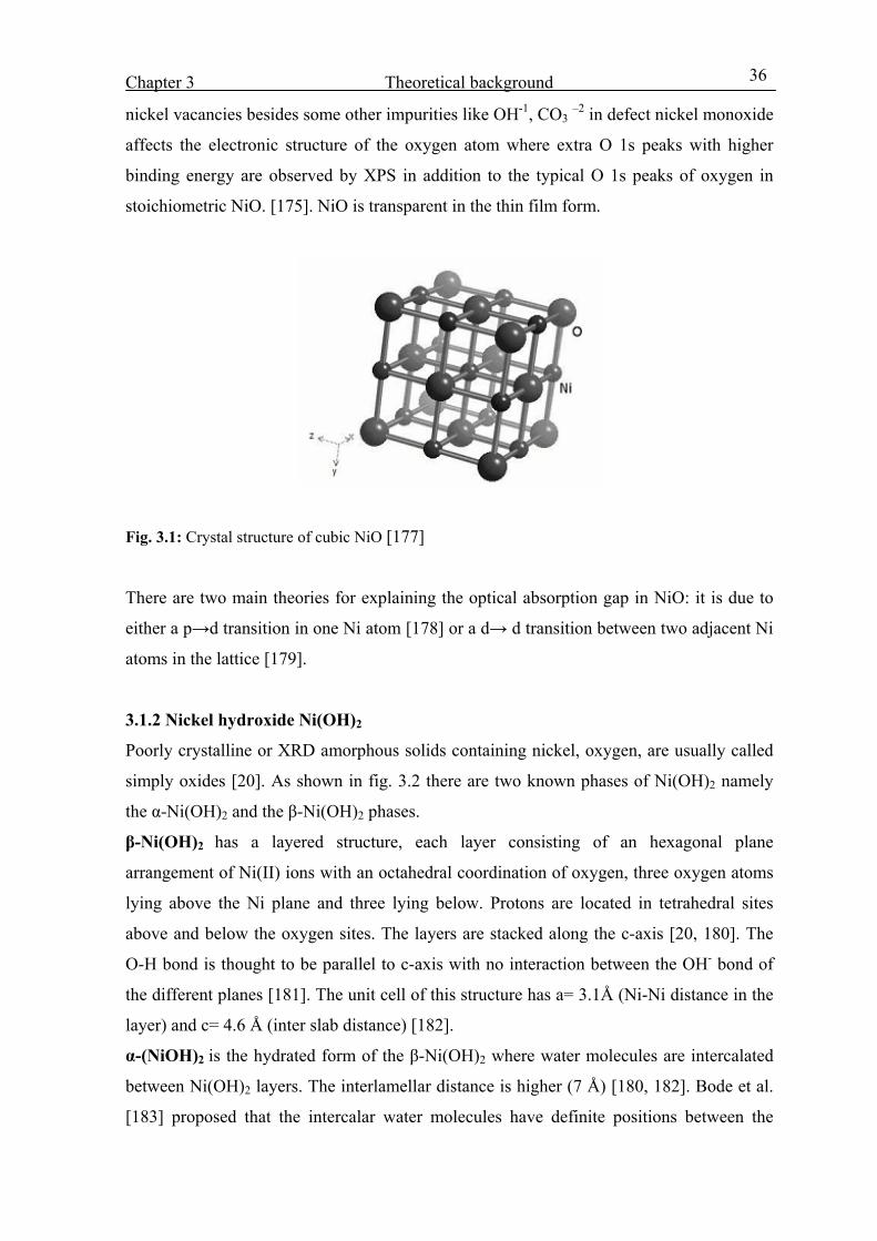
Chapter 3 Theoretical background
36
nickel vacancies besides some other impurities like OH-1, CO3 –2 in defect nickel monoxide
affects the electronic structure of the oxygen atom where extra O 1s peaks with higher
binding energy are observed by XPS in addition to the typical O 1s peaks of oxygen in
stoichiometric NiO. [175]. NiO is transparent in the thin film form.
Fig. 3.1: Crystal structure of cubic NiO [177]
There are two main theories for explaining the optical absorption gap in NiO: it is due to
either a p→d transition in one Ni atom [178] or a d→ d transition between two adjacent Ni
atoms in the lattice [179].
3.1.2 Nickel hydroxide Ni(OH)2
Poorly crystalline or XRD amorphous solids containing nickel, oxygen, are usually called
simply oxides [20]. As shown in fig. 3.2 there are two known phases of Ni(OH)2 namely
the α-Ni(OH)2 and the β-Ni(OH)2 phases.
β-Ni(OH)2 has a layered structure, each layer consisting of an hexagonal plane
arrangement of Ni(II) ions with an octahedral coordination of oxygen, three oxygen atoms
lying above the Ni plane and three lying below. Protons are located in tetrahedral sites
above and below the oxygen sites. The layers are stacked along the c-axis [20, 180]. The
O-H bond is thought to be parallel to c-axis with no interaction between the OH- bond of
the different planes [181]. The unit cell of this structure has a= 3.1Å (Ni-Ni distance in the
layer) and c= 4.6 Å (inter slab distance) [182].
α-(NiOH)2 is the hydrated form of the β-Ni(OH)2 where water molecules are intercalated
between Ni(OH)2 layers. The interlamellar distance is higher (7 Å) [180, 182]. Bode et al.
[183] proposed that the intercalar water molecules have definite positions between the

Chapter 3 Theoretical background
37
layers where there is a quasi-compact stacking of OH-H2O-OH. The number of water
molecules is defined according to the formula 3Ni(OH)22H2O [183].
This model was rejected by Le Bihan [184] and McEwan [185] who proposed a
turbostratic structure consisting of equidistant randomly oriented Ni(OH)2 layers separated
by intercalary water molecules bonded to hydroxyl group by hydrogen bond.
An α-Ni(OH)2 to β-Ni(OH)2 phase transformation is possible by aging in their mother
solution or by hydrolysis. In the first case the crystal growth proceeds by joining the
primary particles in the solution. In water the turbostratic α-Ni(OH)2 seems to be dissolved
slowly in water and β-Ni(OH)2 is formed by nucleation and growth from the solution
[181]. Both Ni(OH)2 compounds are transparent in thin film form.
3.1.3 Nickel oxihydroxide NiOOH
Nickeloxihydroxide, NiOOH, having Ni with a higher oxidation state (+3) also exists in
two main phases β-NiOOH and γ-NiOOH [181]. Both are colored compounds.
The β-Ni(OH)2 phase can be oxidized to β-NiOOH phase by removing one proton and one
electron without significant structural deformation (see fig. 3.2) [182]. This is associated
with a volume expansion (c = 4.85 Å) [20, 180, 182] due to the electrostatic repulsion
between the oxygen atoms in the adjacent layers after removing the protons[20, 182].
Fig. 3.2: Schematic diagram of the structure of the difference Ni(OH)2 and NiOOH phases [186].
There is also a complete family of γ-NiOOH compounds. In general it is represented by the
formula AxHy(H2O)z.NiO2 where A represents an alkali ion (most probable K+or Na+ ).
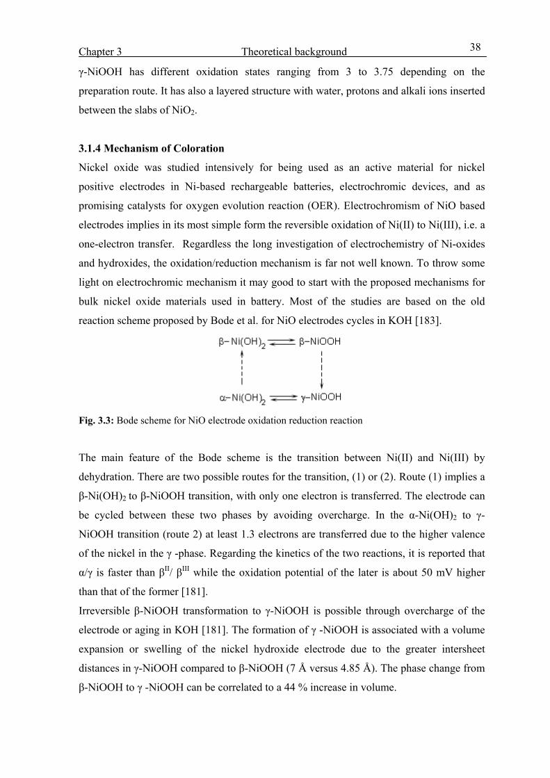
Chapter 3 Theoretical background
38
γ-NiOOH has different oxidation states ranging from 3 to 3.75 depending on the
preparation route. It has also a layered structure with water, protons and alkali ions inserted
between the slabs of NiO2.
3.1.4 Mechanism of Coloration
Nickel oxide was studied intensively for being used as an active material for nickel
positive electrodes in Ni-based rechargeable batteries, electrochromic devices, and as
promising catalysts for oxygen evolution reaction (OER). Electrochromism of NiO based
electrodes implies in its most simple form the reversible oxidation of Ni(II) to Ni(III), i.e. a
one-electron transfer. Regardless the long investigation of electrochemistry of Ni-oxides
and hydroxides, the oxidation/reduction mechanism is far not well known. To throw some
light on electrochromic mechanism it may good to start with the proposed mechanisms for
bulk nickel oxide materials used in battery. Most of the studies are based on the old
reaction scheme proposed by Bode et al. for NiO electrodes cycles in KOH [183].
Fig. 3.3: Bode scheme for NiO electrode oxidation reduction reaction
The main feature of the Bode scheme is the transition between Ni(II) and Ni(III) by
dehydration. There are two possible routes for the transition, (1) or (2). Route (1) implies a
β-Ni(OH)2 to β-NiOOH transition, with only one electron is transferred. The electrode can
be cycled between these two phases by avoiding overcharge. In the α-Ni(OH)2 to γ-
NiOOH transition (route 2) at least 1.3 electrons are transferred due to the higher valence
of the nickel in the γ -phase. Regarding the kinetics of the two reactions, it is reported that
α/γ is faster than βII/ βIII while the oxidation potential of the later is about 50 mV higher
than that of the former [181].
Irreversible β-NiOOH transformation to γ-NiOOH is possible through overcharge of the
electrode or aging in KOH [181]. The formation of γ -NiOOH is associated with a volume
expansion or swelling of the nickel hydroxide electrode due to the greater intersheet
distances in γ-NiOOH compared to β-NiOOH (7 Å versus 4.85 Å). The phase change from
β-NiOOH to γ -NiOOH can be correlated to a 44 % increase in volume.

Chapter 3 Theoretical background
39
Sac-Epee et al [180] proposed another mechanism (see fig. 3.4) where the main difference
with the Bode scheme is the possibility of a direct transformation of γ–NiOOH to
β-Ni(OH)2.
Fig. 3.4: Sac-Epee scheme for NiO electrode oxidation reduction reaction [180]
There are many problems risen on applying these schemes, the most important being that
the stoichiometry of the compounds included in the schemes is not as simple as seems in
the model e.g., the formula of α -Ni(OH)2 and γ -NiOOH also include cations and anions
intercalated and the oxidized form also contained NiIV [187].
The electrochromic mechanisms of the nickel oxides thin films based on the above
schemes are still unclear although numerous textbook examples of the intercalation
kinetics have been published. There are three main reactions based on studies of NiO thin
films in aqueous media. The reactions differ according to the composition of the layer
(NiO or Ni(OH)2) and on the intercalated ions (H+ or OH-). They are:
Ni(OH)2 ↔ NiOOH + H+ + e- (3.1)
Ni(OH)2 +OH- ↔ NiOOH + H2O + e- (3.2)
NiO+ OH- ↔ NiOOH + e- (3.3)
NiO and Ni(OH)2 are transparent while NiOOH is colored in thin film form.
Most of the reports accept the general mechanism of equation (3.1) without any detalied
investigations [84, 91, 93, 100, 188, 189], while others accept equation (3.2) [79, 103, 121]
and (3.3) [103]. Fantini at al. [97] beleived that the reaction starts according to equation
(3.2) then NiOOH is reduced to Ni(OH)2 and the reaction proceeds according to equation
(3.1).
Some others performed details measurements to find out the meachnism for the redox
reaction. Surca et al. [83] performed detailed IR measurements of bleached and colored
sol-gel NiO layers. They found that part of the structure of as-deposited layers has a
Chapter 3 Theoretical background
40
turbostratic α-Ni(OH)2 structure which contains foreign ions (SO4, CO2, OH and H2O).
Small amount of a bad crystalline β-Ni(OH)2 phase has been detected. The colored layers
have an oxohydroxy Ni+3 phase which was confirmed by the presence of hydrogen bonded
OH-O stretching mode. Their final conclusion was that the coloration/bleaching
mechanism of the films takes place by intercalation of OH- with a progressive development
of the β-Ni(OH)2 and β-NiOOH phases accompanying the bleaching/coloring cycles.
A different reaction was proposed by Azen et al. for sputtered layers [116].
NiO + H2O ↔ NiOOH +H+ +e- (3.4)
In such reaction neither Ni(OH)2 nor OH- are important for the electrochromism of NiO
layers, but only water which may present initially in the pores of the oxide film is needed.
OH- groups do not enter the grains upon coloration, and NiOOH is formed on the grain
surface. This does not contradict the condense structure of NiO. This proposal is in
agreement with the absence of any structural changes observed during the coloration and
with the importance of the grain boundary for the efficiency of electrochromic layers
[116].
Decker´s group [190] went in a different way to prove that the water in the aqueous
electrolyte has no role in the coloration/bleaching reactions. A layer was covered with a Pd
film to work as a barrier for water insertion in the layer when cycled in aqueous
electrolyte. A similar layer was tested in dry H+ gaseous environment. The two layers
could be bleached equally fast and efficiently. An increase in the compressive stress was
noticed during the bleaching cycle of layers deposited on flexible substrate. The sputtered
layers were considered to be a mixture of two phases, NiO and Ni3O4 and the proposed
reaction was [190]
NiO + Ni3O4 +2 H+ + e- ↔ Ni(OH)2 + 3NiO (3.5)
where NiO and Ni(OH)2 are transparent while Ni3O4 is coloured.
Rougier et al. [124] put a well organized proposal to explain the electrochromic redox
reactions for PLD NiO layer. In the beginning Ni(OH)2 is formed chemically on the
surface of NiO by immersion in KOH according to NiO + H2O →Ni(OH)2. Then the
reaction goes in the direction Ni(OH)2/NiOOH. The oxidized phase (NiOOH) is not stable
Chapter 3 Theoretical background
41
and is dissolved in KOH and a new layer of NiO has to transform into Ni(OH)2 to continue
the process.
Considering the electrochromism of NiOx layers in aprotic electrolytes containing Li+ salt,
Passerini [191] was the first to show that nickel oxide samples can undergo a reversal
lithium intercalation-deintercalation process accompanied by relevant electrochromic
effect.
Later [192, 193] Li+ intercalation in the NiOx layer has been divided into two processes,
activation period which involves irreversible uptake of Li+ in the host structure of NiOx
layer. This followed by a reversible intercalation/deintercalation accompanied
electrochromic bleaching/coloration process. The following two reaction describes the
whole process
NiOx + yLi+ + ye- → LiyNiOx (3.6)
LiyNiOx + zLi+ + ze- ↔ Liy+zNiOx (3.7)
To further substantiate this model, Passerini et al. [193] measured the expansion of the host
oxide matrix during the activation period by determining the mechanical stress induced by
ion intercalation. The initial increase in stress at the negative potential indicates a slow ion
diffusion in the layer. By reversing the sign of the current the induced mechanical stress
remained unchanged. This process involved 20 mC/cm2µm. When higher charges is used
the extra stress became reversible.
Investigations based on cyclic voltammetric, impedance analysis stress measurement
scanning electron microscopy showed that the intercalation of lithium induces phase
changes in the nickel oxide structure [194]. A diffusion coefficient of about
1.0x10⁻¹¹ cm2S-1 at room temperature was estimated.
Cathodic electrochromic behavior was noticed upon overcharge of nickel oxide electrode.
A small polaron model was proposed to explain the modification of the nickel oxide layer
upon lithium intercalation [195]. The model assumed that on charging, the nickel oxide
changes progressively from a degenerated metal like p-type semiconductor in the pristine
state to a p-type semiconductor in the low intercalation state (QLi<140 mC/cm2µm), then to
a n-type semiconductor in the high intercalated state (QLi> 140 mC/cm2. µm) and again to
a degenerated, metal like material in the full intercalated state.
Chapter 4 Experimental methodology
42
Chapter 4
Experimental methodology
4.1 Preparation of the sols and deposition of layers 4.1.1 NiO-TiO2 sols and layers
NiO-TiO2 sol was prepared according to an recipe developed at INM [89]. 0.5 M solution
was prepared by dissolving 23.38 g of Ni(CH3COO)24H2O in 200 ml ethanol at room
temperature with continuous stirring for 7 hours. Then 7.8 g of titanium n-propoxide
Ti(C3H7O)4 were dissolved in 50 ml ethanol and added to the Ni solution in a glove box
filled with nitrogen (humidity ≤ 5%) in order to obtain Ni molar concentration of
33 mol %. The sol was then stirred at room temperature for 30 min. and, upon completion
filtered using a 0.2 µm filter. Apart from this composition, series of solution with total
concentration of 0.5 M but with different Ni molar concentrations ranging from 100 to
10 % were also studied.
NiO-TiO2 were deposited by the dip coating process (withdrawal speed of 3 mm/s, 20 °C,
RH = 38 %) onto 10 x10 cm2 float glass and commercial conducting SnO2:F coated glass
having a sheet resistance of 17 Ω/ (K-glass). The layers then heat treated in air at a rate of
2 K/min up to the desired temperature and then the system was left at this temperature for
about 30 min.
Up to 3 layers have been deposited. For this purpose the same heat treatment was
performed after each deposition. Also single layers having different thickness values have
been deposited by changing the withdrawing speed from 0.5 to 4 mm/s.
4.1.2 (CeO2)-(TiO2) sols and layers
The (CeO2)x(TiO2)1-x sol was prepared according to a recipe developed at INM [196]. First
24.4254 g Ce(NO3)3⋅6H2O were dissolved in 125 ml absolute ethanol (0.45 mol/l Ce), then
19.5429 g Ti(i-OPr)4 were dissolved in 125 ml absolute ethanol (0.55 mol/l Ti) and added
to the cerium nitrate ethanol solution in a glove box with nitrogen atmosphere. These
solutions were aged at 30°C during several days under mechanical stirring in closed glass
vessels to prevent rapid a precipitation of the Ti alkoxide due to hydrolysis.
The CeO2-TiO2 layers were deposited on pre-treated K-glass by the dip-coating technique
with a withdrawal rate of 4 mm/s at 20 °C with 38 % air humidity. The layers were then
Chapter 4 Experimental methodology
43
heated from room temperature up to 550 °C with a heating rate of 2.5 K/min, maintained at
550 °C for 1 hour and then cooled down to room temperature.
4.1.3 Nb2O5:Mo sols and layers
The Nb2O5:Mo sol was prepared according to a INM recipe [197]. First 0.12 M of
H3[P(Mo3O10)4]·H2O were weighted in glove box under nitrogen atmosphere and dissolved
in 125 ml ethanol. Second 125 ml anhydrous ethanol was dropped to 0.4 M NbCl5 using
pressure equalizer in order to obtain niobium chloroethoxide sol [144]. 30 ml acetic acid
(99-100 %) and the molybdenum sol were added then to this during stirring in about 5 min.
The mixture was put into an ice bath and subject to an ultrasonic treatment for 4 hours.
Aging at temperature of 20 °C in a closed glass recipient for two days is needed before
using the sol for coating.
Double Nb2O5:Mo layers were deposited onto pre-treated K-glass by dip coating process at
a withdrawal speed of 4 mm/s. The first deposited layer was dried for 30 min at 100 °C in
an oven under synthesis air. Another layer was then deposited and dried in the same way
and the double layers were sintered directly at 500 °C for 30 min, then cooled down to
room temperature.
4.1.4. Anti corrosion layers
A 0.5 M of Al2O3 sol was prepared by dissolving 12.3 g of Aluminium tri-sec butylate
(C12H27AlO3) in 100 ml of butanol under stirring in glove box..
A 0.5M of ZrO2 was prepared by dissolving 16.35 g of zirconium n-propoxide
(Zr(OC3H7)4) in 100 ml of isopropanol under stirring in glove box..
A 0.5 M of TiO2 sol was obtained by dissolving 14.2 g of Titanium n-propoxide
(Ti(C3H7O)4) in 100 ml of ethanol.
The layers was deposited on the top of NiO-TiO2 coating by dip coating technique at
withdrawal speed of 0.5 mm/s and sintered at 300 °C.
4.2. Synthesis of electrolyte 4.2.1 liquid KOH electrolyte
5.6 g of KOH crystal was dissolved in 100 ml of bidistalled water under stirring for a few
minutes to get aqueous KOH electrolyte of 1 molar concentration.
4.2.2 Gel KOH electrolyte
1.8 g of starch (C6H10O5)n was dissolved in 30 ml of bidistilled water at room temperature.
The sol temperature was raised gradually to 85 °C with continuous stirring for 3 hours. The

Chapter 4 Experimental methodology
44
sol then left to cool down to 50 °C with stirring. Small amount of KOH was then dissolved
in 5 ml bidistilled water and added to the starch sol. 1.5 g of glycerol (C3H8O3) was added
and stirred for one min. 0.5 g formaldehyde (CH2O) could be added to increase the cross
linking of the electrolyte. The electrolyte should be filled in the devices as soon as it is
prepared.
4.2.3 Nanocomposite electrolyte
A solid ionic conductor has been prepared according to a method used at INM [198, 199].
The composition is based on glycidoxypropyltrimethoxysilane (GPTS), LiClO4, Zr(OnPr)4
and tetraethylene glycol (TEG). GPTS serves as network formers, whereas TEG acts as a
plasticizer. Lithium perchlorate is the conducting salt and Zr(OnPr)4 is added as a starter
for thermal curing. Dried LiClO4 was first dissolved in a mixture of TEG and
prehydrolysed GPTS. TEOS and Zr(OnPr)4 were then added. The volatiles were removed
by rotary evaporation immediately prior to the filling it in the EC windows.
4.3 Mounting of EC-devices The preparation of the EC devices was performed first by gluing 1 mm thick, 3 mm wide a
adhesive tape at the edges of one of the functional coatings (e.g. k-glass/EC layer) then the
other coated substrate was put on the first substrate in a way that the two coatings face
each other inside the assembled window. A 1 cm width adhesive copper tape was pressed
to the free edge of each substrate for electrical connection. The electrolyte was injected in
the mounted cells using a syringe. In the case of ormolyte the devices were then heated up
to 105 °C for 12 hours. For EC devices made with wet electrolyte, the amount of water (1
to 3 wt%) was first dissolved into the electrolyte before filling the EC device
4.4 Thermal analysis (DTA/TG/IR/MS) Simultaneous DTA and TG have been performed on NiO-TiO2 xerogels dried overnight
(Ni concentration 75 mol %) using a Netzsch STA 449C/3G Jupiter equipment coupled to
a Mass spectroscopy (MS) (QMS 403C Aeolos) and an Infrared spectrometer (FTIR)
(Tensor 27-FTIR, Brucker). The xerogels were grounded in a mortar to get a fine powder.
33.3 mg of the powder was heated in synthetic air in an Al2O3 crucible up to 600°C at a
heating rate of 2K/min.
The Differential Thermal analysis (DTA) is a technique that provides information on the
chemical reactions, phase transformations, and structural changes that occur in a sample
Chapter 4 Experimental methodology
45
during a heat-up or a cool-down process. DTA measures the differences in energy released
or absorbed, and the changes in heat capacity of materials as a function of temperature.
Thermogravimetry (TG) is a technique by which the mass changes of a sample is
monitored while the sample is subjected to a temperature-time program in a well defined
atmosphere.
The combination of Thermal Analysis and Spectroscopic Analysis delivers extremely
valuable information for material characterization and phase changes during thermal
decomposition. The spectroscopic techniques depend on Evolved Gas Analysis (EGA).
The most common ones are:
Mass spectroscopy (MS) is a technique of determining the nature and amount of volatile
product formed during thermal analyses. During real-time DTA/TG, the mass spectrometer
ionises the evolved gases, which are identified by their characteristic fragments. The
spectrometer can either scan over a range of 0-300 amu or monitor individual ions of
interest. The last method was followed in our measurements.
aaInfrared spectroscopy (FT-IR) is a technique for identification of gases released directly
from the sample or during thermal treatment. IR spectroscopy is a classical technique,
which depends upon the interaction of infrared radiation with the vibrating dipole moments
of molecules. It gives, with the exception of homonuclear diatomic and noble gases, a
characteristic spectrum for each substance.
Gram-Schmidt orthogonalization (GS) is a powerful data analysis tool [200], used to detect
the presence of infrared radiation absorbing species evolved in the real time between 400
and 4000 cm-1.
4.5 Thickness measurement The thickness of the layers was determined by a TENCOR P-10 surface profilometer.
Samples were scratched deeply with a sharp item at three different positions (for more
accuracy) few minutes after dip coating during the drying stage. After heat treatment, the
surface of the sample was scanned by a diamond stylus through the scratches from one
edge to the other. The step height between the layer surface and FTO at the scratch
represents the layer thickness.
Chapter 4 Experimental methodology
46
4.6 Morphology and structure analysis 4.6.1 Surface morphology studied by Scanning Electron Microscopy (SEM)
Scanning Electron Microscopy (SEM) of the surface has been obtained using a JEOL JSM-
6400F equipment using the secondary electron signal excited at 10 k eV primary beam. A
very thin conducting gold was sputtered on the surface of the sample before testing it to get
charge free surface.
4.6.2 Layer morphology studied by Transmittance Electron Microscopy (TEM)
Transmittance Electron Microscopy (TEM) measurements have been made with fresh,
bleached and colored thin rasped layers using a JEOL.JEM-2010 Gatan MSC equipment.
4.6.3 X-ray diffraction
X-ray diffraction is an investigation method which can identify an unknown mineral, or
characterize the atomic-scale structure of an already identified mineral The structural
investigation of fresh triple NiO-TiO2 layers deposited on float glass and heat treated from
250 to 500 °C was achieved using X-ray diffraction (XRD) (X’Pert Philips- MPD,
CuKα1,2) in the range 26 ° < 2θ < 80 ° at 0.3° grazing incidence and scan steps of 0.02°.
The crystallite size were determined from the half width of the full maxima (HWFM) of
specific XRD peaks using the Scherrer equation. To check the effect of Ni molar ratio,
XRD of layers with different Ni molar concentration ranging from 33 to 90 % deposited on
float glass and sintered at 400 °C were also measured.
To test a possible change of the structure during the EC process, triple layers have been
also deposited onto 4x10 cm2 ITO coated glass substrate (Asahi Glass). The NiO-TiO2
layers have been cycled in 1 M KOH electrolyte up to 270 (CV) cycles (see section 4.7),
then disconnected at the positive potential (colored state +1 V vs SCE), or at the negative
potential (bleached state –0.6 V vs. SCE) and dried in air before performing the XRD
(range 10 < 2θ< 90 °, 0.02 ° steps). The colored layers remained deeply coloured within
the X-ray scan time of 12 hour. For comparison, fresh layers have been also measured in
the same way.
4.7 Electrochemical characterization Electrochemical measurements have been carried on using a three electrode cell shown in
fig. 4.1. The working electrode was the layer to be characterized deposited on K-glass, the
counter electrode was a Platinum foil of 2.1 cm2 area, the reference electrode was
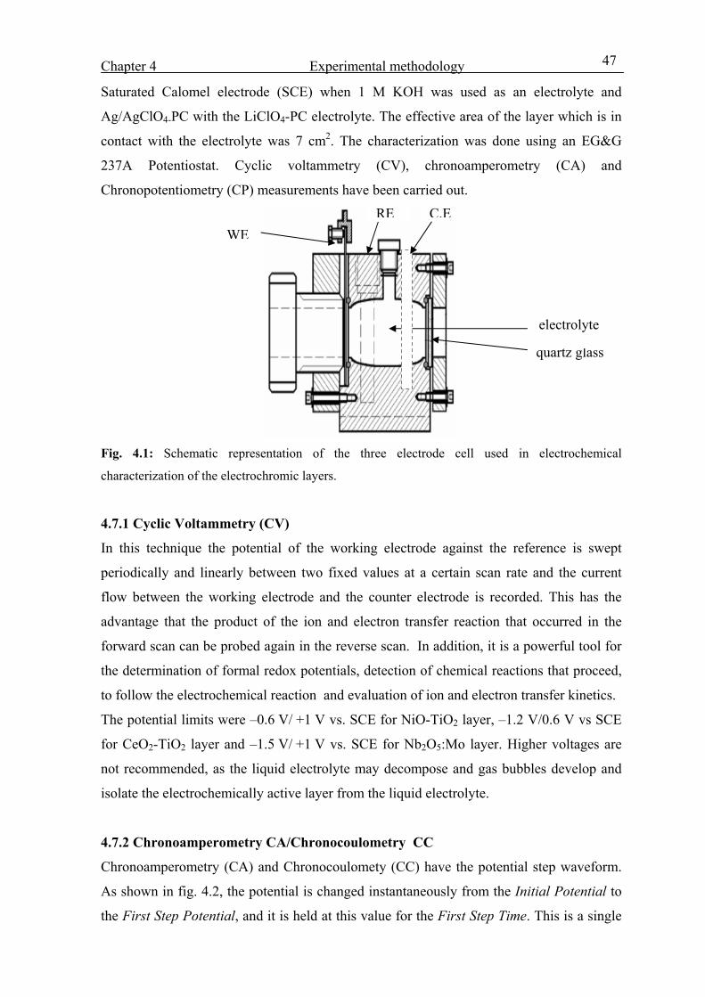
Chapter 4 Experimental methodology
47
Saturated Calomel electrode (SCE) when 1 M KOH was used as an electrolyte and
Ag/AgClO4-PC with the LiClO4-PC electrolyte. The effective area of the layer which is in
contact with the electrolyte was 7 cm2. The characterization was done using an EG&G
237A Potentiostat. Cyclic voltammetry (CV), chronoamperometry (CA) and
Chronopotentiometry (CP) measurements have been carried out.
Fig. 4.1: Schematic representation of the three electrode cell used in electrochemical
characterization of the electrochromic layers.
4.7.1 Cyclic Voltammetry (CV)
In this technique the potential of the working electrode against the reference is swept
periodically and linearly between two fixed values at a certain scan rate and the current
flow between the working electrode and the counter electrode is recorded. This has the
advantage that the product of the ion and electron transfer reaction that occurred in the
forward scan can be probed again in the reverse scan. In addition, it is a powerful tool for
the determination of formal redox potentials, detection of chemical reactions that proceed,
to follow the electrochemical reaction and evaluation of ion and electron transfer kinetics.
The potential limits were –0.6 V/ +1 V vs. SCE for NiO-TiO2 layer, –1.2 V/0.6 V vs SCE
for CeO2-TiO2 layer and –1.5 V/ +1 V vs. SCE for Nb2O5:Mo layer. Higher voltages are
not recommended, as the liquid electrolyte may decompose and gas bubbles develop and
isolate the electrochemically active layer from the liquid electrolyte.
4.7.2 Chronoamperometry CA/Chronocoulometry CC
Chronoamperometry (CA) and Chronocoulomety (CC) have the potential step waveform.
As shown in fig. 4.2, the potential is changed instantaneously from the Initial Potential to
the First Step Potential, and it is held at this value for the First Step Time. This is a single
electrolyte
WERE
quartz glass
C.E
electrolyte electrolyte
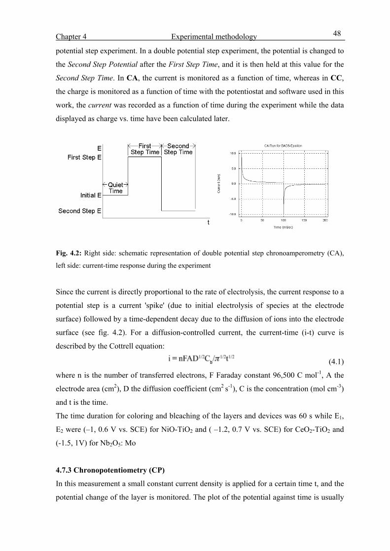
Chapter 4 Experimental methodology
48
potential step experiment. In a double potential step experiment, the potential is changed to
the Second Step Potential after the First Step Time, and it is then held at this value for the
Second Step Time. In CA, the current is monitored as a function of time, whereas in CC,
the charge is monitored as a function of time with the potentiostat and software used in this
work, the current was recorded as a function of time during the experiment while the data
displayed as charge vs. time have been calculated later.
Fig. 4.2: Right side: schematic representation of double potential step chronoamperometry (CA),
left side: current-time response during the experiment
Since the current is directly proportional to the rate of electrolysis, the current response to a
potential step is a current 'spike' (due to initial electrolysis of species at the electrode
surface) followed by a time-dependent decay due to the diffusion of ions into the electrode
surface (see fig. 4.2). For a diffusion-controlled current, the current-time (i-t) curve is
described by the Cottrell equation:
(4.1)
where n is the number of transferred electrons, F Faraday constant 96,500 C mol-1, A the
electrode area (cm2), D the diffusion coefficient (cm2 s-1), C is the concentration (mol cm-3)
and t is the time.
The time duration for coloring and bleaching of the layers and devices was 60 s while E1,
E2 were (–1, 0.6 V vs. SCE) for NiO-TiO2 and ( –1.2, 0.7 V vs. SCE) for CeO2-TiO2 and
(-1.5, 1V) for Nb2O5: Mo
4.7.3 Chronopotentiometry (CP)
In this measurement a small constant current density is applied for a certain time t, and the
potential change of the layer is monitored. The plot of the potential against time is usually

Chapter 4 Experimental methodology
49
a sigmoid curve with various plateaus. Each plateau corresponds to a redox potential of a
certain electrochemical reaction. The total inserted charge density can be calculated by
multiplying the total time of experiment by the applied current density Q = i * t
Current density of ±5µA/cm2 was applied for different time periods in this work.
4.8 Optical properties In-situ transmittance measurement was carried out during the electrochemical
measurements at the wavelength 550 nm using a Cary 5E UV-VIS-NIR spectrophotometer
from Varian. Spectral transmittance of the layers have been also measured in the spectral
range 200-1200 nm using the same instrument. The measurement were carried out for the
layers in the three electrode cell at normal incident angle against a reference cell that have
a float glass substrate in the place of the working electrode. The transmittance of the
devices is measured in the spectral range 300 to 3000 nm against air as a reference.
The change in optical density (∆OD) was calculated using the measured transmittance of
the layer or device in the colored (Tc) and bleached (Tb) state by applying the equation
∆OD = Log10 Tb/Tc
4.9 Electrochemical quartz crystal microbalance Quartz crystal microbalance (QCM) uses a piezoelectric crystal oscillating at a very sharp
defined frequency. Small mass changes of the crystal surface shift this frequency. Both
sides of the crystal are coated with a gold electrode. The system is placed in an
electrochemical cell that allows recording simultaneously the electrochemical parameters
and the mass changes.
The EQCM measurements were made using a Maxtek, Inc microbalance connected to
VMP2 multi channel potentiostat, in order to control the potential applied to the crystal,
and to a computer. The frequency changes and calculating the corresponding mass changes
were obtained using the RQCM data logging software. The electrochemical cell used was a
double wall glass flask connected to a thermostated cycling water to control the
temperature. The NiO-TiO2 coated quartz crystal (quartz crystal 5 MHz AT-cut from
maxtek, Inc) was used as working electrode, a platinum mesh as counter electrode and
SCE as a reference electrode. 1 M KOH was used as electrolyte. The electrodes were fixed
in three special holes in the rubber cap of the electrochemical cell. Changes in the quartz
crystal resonant frequency were converted to mass changes using the Sauerbrey equation
[201].
Chapter 4 Experimental methodology
50
mA
ff
Δ⎟⎟⎟
⎠
⎞
⎜⎜⎜
⎝
⎛−=Δ
μρ
2
02
(4.2)
where Δf is the change in frequency (Hz), Δm the mass change (µg), f0 is the resonant
frequency of the used quartz crystal (5 MHz AT-cut), ρ is the density of the quartz (2.648
g/cm3), A is the area of the electrode (1.37 cm3) and µ is the quartz shear modulus
(2.947×10¹¹ g.s-2cm-1). The minus sign means that the resonant frequency shifts to lower
values by increasing the mass of the quartz crystal. The value between parentheses was
calculated and the above equation can be written in the simple form
mf C fΔ−=Δ (4.3)
where Cf is the sensitivity factor of the crystal In our case Cf = 56.6 Hzµg-1cm2.
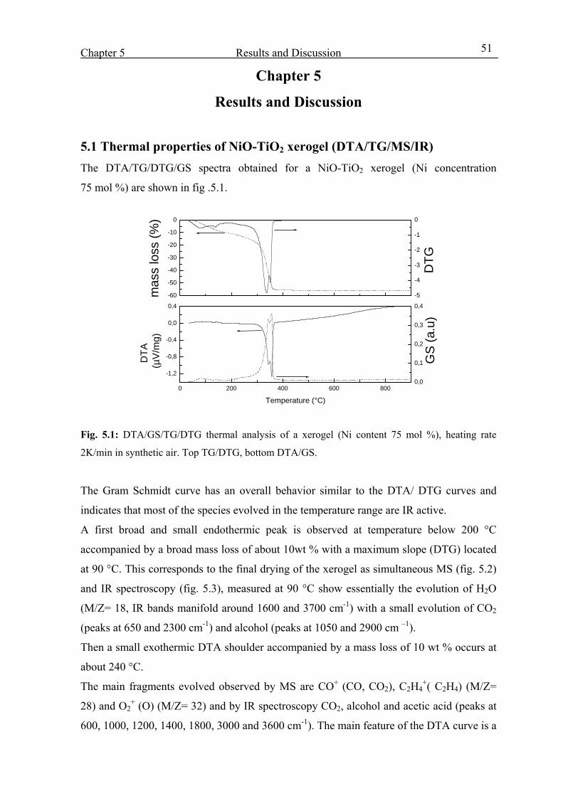
Chapter 5 Results and Discussion
51
Chapter 5
Results and Discussion
5.1 Thermal properties of NiO-TiO2 xerogel (DTA/TG/MS/IR) The DTA/TG/DTG/GS spectra obtained for a NiO-TiO2 xerogel (Ni concentration
75 mol %) are shown in fig .5.1.
-1,2
-0,8
-0,4
0,0
0,4
-60
-50
-40
-30
-20
-10
0
0 200 400 600 8000,0
0,1
0,2
0,3
0,4
-5
-4
-3
-2
-1
0
GS
(a.u
)
mas
s lo
ss (%
)
DTA
(µ
V/m
g)
DTG
Temperature (°C)
Fig. 5.1: DTA/GS/TG/DTG thermal analysis of a xerogel (Ni content 75 mol %), heating rate
2K/min in synthetic air. Top TG/DTG, bottom DTA/GS.
The Gram Schmidt curve has an overall behavior similar to the DTA/ DTG curves and
indicates that most of the species evolved in the temperature range are IR active.
A first broad and small endothermic peak is observed at temperature below 200 °C
accompanied by a broad mass loss of about 10wt % with a maximum slope (DTG) located
at 90 °C. This corresponds to the final drying of the xerogel as simultaneous MS (fig. 5.2)
and IR spectroscopy (fig. 5.3), measured at 90 °C show essentially the evolution of H2O
(M/Z= 18, IR bands manifold around 1600 and 3700 cm-1) with a small evolution of CO2
(peaks at 650 and 2300 cm-1) and alcohol (peaks at 1050 and 2900 cm –1).
Then a small exothermic DTA shoulder accompanied by a mass loss of 10 wt % occurs at
about 240 °C.
The main fragments evolved observed by MS are CO+ (CO, CO2), C2H4+( C2H4) (M/Z=
28) and O2+ (O) (M/Z= 32) and by IR spectroscopy CO2, alcohol and acetic acid (peaks at
600, 1000, 1200, 1400, 1800, 3000 and 3600 cm-1). The main feature of the DTA curve is a
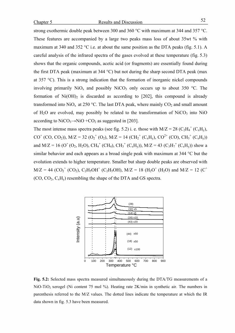
Chapter 5 Results and Discussion
52
strong exothermic double peak between 300 and 360 °C with maximum at 344 and 357 °C.
These features are accompanied by a large two peaks mass loss of about 35wt % with
maximum at 340 and 352 °C i.e. at about the same position as the DTA peaks (fig. 5.1). A
careful analysis of the infrared spectra of the gases evolved at these temperature (fig. 5.3)
shows that the organic compounds, acetic acid (or fragments) are essentially found during
the first DTA peak (maximum at 344 °C) but not during the sharp second DTA peak (max
at 357 °C). This is a strong indication that the formation of inorganic nickel compounds
involving primarily NiOx and possibly NiCO3 only occurs up to about 350 °C. The
formation of Ni(OH)2 is discarded as according to [202], this compound is already
transformed into NiOx at 250 °C. The last DTA peak, where mainly CO2 and small amount
of H2O are evolved, may possibly be related to the transformation of NiCO3 into NiO
according to NiCO3→NiO +CO2 as suggested in [203].
The most intense mass spectra peaks (see fig. 5.2) i. e. those with M/Z = 28 (C2H4+ (CxHy),
CO+ (CO, CO2)), M/Z = 32 (O2+ (O2), M/Z = 14 (CH2
+ (CxHy), CO2+ (CO), CH3+ (CxHy))
and M/Z = 16 (O+ (O2, H2O), CH4+ (CH4), CH3
+ (CxHy)), M/Z = 43 (C3H7+ (CxHy)) show a
similar behavior and each appears as a broad single peak with maximum at 344 °C but the
evolution extends to higher temperature. Smaller but sharp double peaks are observed with
M/Z = 44 (CO2+ (CO2), C2H5OH+ (C2H5OH), M/Z = 18 (H2O+ (H2O) and M/Z = 12 (C+
(CO, CO2, CxHy) resembling the shape of the DTA and GS spectra.
0 100 200 300 400 500 600 700 800 900
x100
x50
x50
(43) x20
(12)
(18)
(44)
Temperature °C
Inte
nsity
(a.u
)
(16) x10
(14) x5(32) x5
(28)
Fig. 5.2: Selected mass spectra measured simultaneously during the DTA/TG measurements of a
NiO-TiO2 xerogel (Ni content 75 mol %). Heating rate 2K/min in synthetic air. The numbers in
parenthesis referred to the M/Z values. The dotted lines indicate the temperature at which the IR
data shown in fig. 5.3 have been measured.
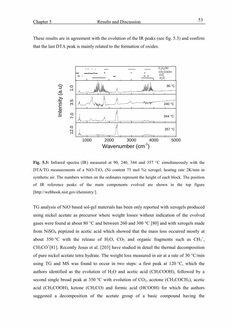
Chapter 5 Results and Discussion
53
These results are in agreement with the evolution of the IR peaks (see fig. 5.3) and confirm
that the last DTA peak is mainly related to the formation of oxides.
1000 2000 3000 4000 5000
1.0
3.5
7.0
12.0
357 °C
Inte
nsity
(a.u
)
Wavenumber (cm-1)
344 °C
90 °C
240 °C
CH3COOHC2H5OH
CO2H2O
Fig. 5.3: Infrared spectra (IR) measured at 90, 240, 344 and 357 °C simultaneously with the
DTA/TG measurements of a NiO-TiO2 (Ni content 75 mol %) xerogel, heating rate 2K/min in
synthetic air. The numbers written on the ordinates represent the height of each block. The position
of IR reference peaks of the main components evolved are shown in the top figure
[http://webbook.nist.gov/chemistry/].
TG analysis of NiO based sol-gel materials has been only reported with xerogels produced
using nickel acetate as precursor where weight losses without indication of the evolved
gases were found at about 80 °C and between 260 and 300 °C [80] and with xerogels made
from NiSO4 peptized in acetic acid which showed that the mass loss occurred mostly at
about 350 °C with the release of H2O, CO2 and organic fragments such as CH3+,
CH3CO+[81]. Recently Jesus et al. [203] have studied in detail the thermal decomposition
of pure nickel acetate tetra hydrate. The weight loss measured in air at a rate of 30 °C/min
using TG and MS was found to occur in two steps: a first peak at 120 °C, which the
authors identified as the evolution of H2O and acetic acid (CH3COOH), followed by a
second single broad peak at 350 °C with evolution of CO2, acetone (CH3COCH3), acetic
acid (CH3COOH), ketone (CH2CO) and formic acid (HCOOH) for which the authors
suggested a decomposition of the acetate group of a basic compound having the

Chapter 5 Results and Discussion
54
composition 0.56Ni(CH3COO)2·0.14Ni(OH)2 produced during the dehydration of the salt
at 120 °C and leading to the formation of NiO and Ni. Ti(Si) xerogel produced from
NiSO4.7H2O peptized by acetic acid also showed a mass loss between 300 and 380 °C with
evolution of CO2 and H2O. However the whole process was somewhat blurred out due to
the cross linking effect of the added silane [93].
5.2 Structural properties a) Thickness and coating appearance
The thickness of single layers made by dip coating process was adjusted by varying the
dip-coating withdrawal speed. For layers made with a Ni concentration of 75 mol % and
sintered at 300°C, a range of thickness between 20 to 100 nm was achieved by varying the
withdrawal speed between 0.5 and 4 mm/s respectively. Thicker coating up to 240 nm have
been achieved by processing multilayers.
SEM pictures of the coatings made with different Ni molar concentration indicate that all
layers are homogeneous without pits or cracks (figure 5.4). All coatings showed a slight
greenish color.
Fig. 5.4: SEM picture for NiO-TiO2 layers (Ni concentration of 75 mol %) deposited on K-glass
and sintered at 300 °C. The accelerating potential was 10 keV, resolution of 1024x1024.
600 nm

Chapter 5 Results and Discussion
55
b) X-ray diffraction and TEM of fresh (uncycled) layers
X-ray diffraction spectra of NiO-TiO2 layers (Ni concentration of 75 mol %) sintered in air
at 250, 300, 400 and 500 °C for 30 min are shown in fig.5.5. The layers sintered at 250 °C
are amorphous and those heat treated at higher temperature exhibit the five peaks of the
Bunsenite cubic nickel oxide structure. The crystallinity of the layers increases with the
sintering temperature and the crystallite size calculated with the (200) peak are 2.5, 4.7 and
8 nm respectively. A slight (200) preferential orientation is observed. No evidence of a
Ni(OH)2, NiOOH and TiO2 crystalline phase is found so that if these compounds exist they
are X-ray amorphous.
30 40 50 60 70 80
0.0
3.0k
6.0k
9.0k
12.0k
15.0k
(222)(311)
(220)
(200)
(111)
Inte
nsity
2θ (degree)
250 °C
300 °C
400 °C500 °C
Fig. 5.5: XRD patterns for NiO-TiO2 layers (Ni concentration of 75 mol %) deposited on float
glass and annealed in air at different temperatures. The vertical lines refer to the Bunsenite nickel
oxide phase (PDF-No. 71-1179).
The TEM picture (Fig. 5.6a) of a fresh (uncycled) rasped thin layer shows the presence of
many very small round crystalline grains with size of about 8 nm, i.e. about 3 times that of
the crystallites, impeded in an amorphous structure.
a
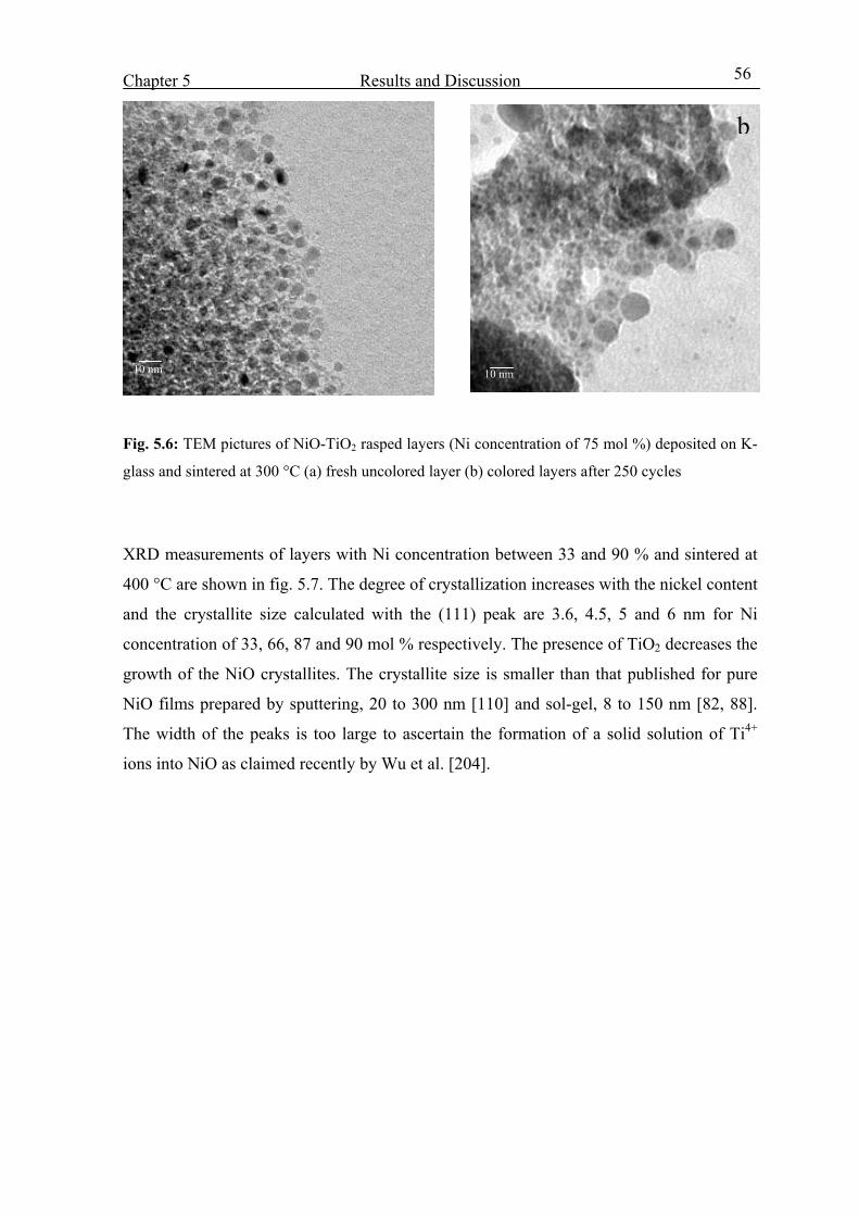
Chapter 5 Results and Discussion
56
Fig. 5.6: TEM pictures of NiO-TiO2 rasped layers (Ni concentration of 75 mol %) deposited on K-
glass and sintered at 300 °C (a) fresh uncolored layer (b) colored layers after 250 cycles
XRD measurements of layers with Ni concentration between 33 and 90 % and sintered at
400 °C are shown in fig. 5.7. The degree of crystallization increases with the nickel content
and the crystallite size calculated with the (111) peak are 3.6, 4.5, 5 and 6 nm for Ni
concentration of 33, 66, 87 and 90 mol % respectively. The presence of TiO2 decreases the
growth of the NiO crystallites. The crystallite size is smaller than that published for pure
NiO films prepared by sputtering, 20 to 300 nm [110] and sol-gel, 8 to 150 nm [82, 88].
The width of the peaks is too large to ascertain the formation of a solid solution of Ti4+
ions into NiO as claimed recently by Wu et al. [204].
b
10 nm 10 nm

Chapter 5 Results and Discussion
57
30 40 50 60 70 800
10k
20k
30k
40k
(222)(311)
(220)
(200)(111) Ni molar concentration90 %87 %66 %50 %33 %
Inte
nsity
(cou
nt/s
)
2θ (degree)
Fig. 5.7: XRD pattern for NiO-TiO2 layers of different Ni molar concentration deposited on float
glass and sintered at 400 0C. The vertical lines refer to the Bunsenite nickel oxide phase (PDF-No.
71-1179).
c) X-ray diffraction and TEM of cycled layers
As shown later in section 5.3, NiO-TiO2 layers can be deeply brown colored
electrochemically. Near grazing incidence (0.3 °) of triple layers (240 nm thick) sintered at
300 °C and cycled in KOH during 270 cycles exhibited the same Bunsenite NiO cubic
structure (fig. 5.8). The presence of new peaks containing hydrogen (e.g. Ni(OH)2,
NiOOH) was not found in any film. The only differences that are observed is a reduction
of the intensity of the Bunsenite peaks, an indication of a process of progressive
amorphization during cycling, and two broad bands in the bleached layer at around 12 °
and 22.5 ° that cannot be attributed to any compounds. The results appear at first sight
rather surprising but do not preclude that Ni(OH)2 or NiOOH are present in the cycled
layers as these compounds can be located on the outermost part of the very small NiO
grains (see fig. 5.6a) and too thin to be detected.
Fig. 5.6b shows a TEM picture of a thin rasped layer in the colored state after 270 CV
cycles and rather large morphology changes are observed. Although some larger grains
(size 10 to 13 nm) are observed, the layer now consists of many smaller particles with size
of about 3 nm i.e. the size of the NiO crystallites (2.5 nm), several of them aggregated in a
filament shape. This clearly shows that the fresh NiO grains have been disaggregated into
their primary crystallites during cycling. This confirms that the colored layers have a more
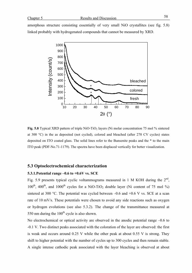
Chapter 5 Results and Discussion
58
amorphous structure consisting essentially of very small NiO crystallites (see fig. 5.8)
linked probably with hydrogenated compounds that cannot be measured by XRD.
10 20 30 40 50 60 70 80 900
100
200
300
400
500
600
700
800
900
1000
*
*
bleached
colored
fresh
Inte
nsity
(cou
nt/s
)
2θ (°)
Fig. 5.8 Typical XRD pattern of triple NiO-TiO2 layers (Ni molar concentration 75 mol % sintered
at 300 °C) in the as deposited (not cycled), colored and bleached (after 270 CV cycles) states
deposited on ITO coated glass. The solid lines refer to the Bunsenite peaks and the * to the main
ITO peak (PDF-No.71-1179). The spectra have been displaced vertically for better visualization.
5.3 Optoelectrochemical characterization 5.3.1.Potential range –0.6 to +0.6V vs. SCE
Fig. 5.9 presents typical cyclic voltammograms measured in 1 M KOH during the 2nd,
100th, 400th, and 1000th cycles for a NiO-TiO2 double layer (Ni content of 75 mol %)
sintered at 300 °C. The potential was cycled between –0.6 and +0.6 V vs. SCE at a scan
rate of 10 mV/s. These potentials were chosen to avoid any side reactions such as oxygen
or hydrogen evolutions (see also 5.3.2). The change of the transmittance measured at
550 nm during the 100th cycle is also shown.
No electrochemical or optical activity are observed in the anodic potential range –0.6 to
-0.1 V. Two distinct peaks associated with the coloration of the layer are observed: the first
is weak and occurs around 0.25 V while the other peak at about 0.55 V is strong. They
shift to higher potential with the number of cycles up to 300 cycles and then remain stable.
A single intense cathodic peak associated with the layer bleaching is observed at about

Chapter 5 Results and Discussion
59
0.15V. It shifts slightly to lower potential value with the number of cycles but remains also
stable after 300 cycles. No electrochemical or optical activity is observed at potential
smaller than –0.2 V. The observed shifts of the anodic and cathodic peaks are a clear
evidence that the composition of the layer evolved continuously during cycling. The same
effect was reported for layers prepared electrochemically [97] and was related to freshly
precipitated electronic insulating Ni(OH)2 material during each cycle.
-0,6 -0,4 -0,2 0,0 0,2 0,4 0,6
-0,8
-0,4
0,0
0,4
0,8
1,2
20
30
40
50
60
70
80
90
T
CV cycles 2 100 400 1000
i (m
A/cm
2 )
Valtage vs SCE (V)T
(%)
Fig. 5.9: Typical CV cycles up to 1000 cycles for a 160 nm thick double NiO-TiO2 layer (Ni
concentration of 75 mol %) heated at 300 °C, potential range -0.6 to 0.6 V vs. SCE, scan rate
10 mV/s in 1 M KOH. The dotted line is the variation of the transmittance (T) measured during the
100th cycle at λ= 550 nm.
The fact that the coloration process occurs only in the anodic range and the bleaching in
the cathodic range only and that both processes are linked to electrochemical processes
(fig. 5.10) is particularly important. The change in the optical density (coloring state) that
varies linearly with the anodic charge is therefore due to an exchange of negatively
charged molecule(s) as discussed later in more detail in section 5.4.
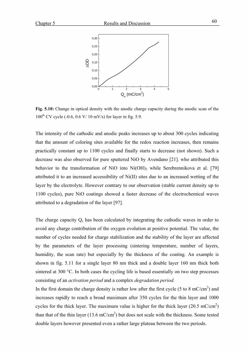
Chapter 5 Results and Discussion
60
0 1 2 3 4 50,00
0,05
0,10
0,15
0,20
0,25
0,30
ΔOD
Qa (mC/cm2)
Fig. 5.10: Change in optical density with the anodic charge capacity during the anodic scan of the
100th CV cycle (-0.6, 0.6 V/ 10 mV/s) for layer in fig. 5.9.
The intensity of the cathodic and anodic peaks increases up to about 300 cycles indicating
that the amount of coloring sites available for the redox reaction increases, then remains
practically constant up to 1100 cycles and finally starts to decrease (not shown). Such a
decrease was also observed for pure sputtered NiO by Avendano [21]. who attributed this
behavior to the transformation of NiO into Ni(OH)2 while Serebrennikova et al. [79]
attributed it to an increased accessibility of Ni(II) sites due to an increased wetting of the
layer by the electrolyte. However contrary to our observation (stable current density up to
1100 cycles), pure NiO coatings showed a faster decrease of the electrochemical waves
attributed to a degradation of the layer [97].
The charge capacity Qc has been calculated by integrating the cathodic waves in order to
avoid any charge contribution of the oxygen evolution at positive potential. The value, the
number of cycles needed for charge stabilization and the stability of the layer are affected
by the parameters of the layer processing (sintering temperature, number of layers,
humidity, the scan rate) but especially by the thickness of the coating. An example is
shown in fig. 5.11 for a single layer 80 nm thick and a double layer 160 nm thick both
sintered at 300 °C. In both cases the cycling life is based essentially on two step processes
consisting of an activation period and a complex degradation period.
In the first domain the charge density is rather low after the first cycle (5 to 8 mC/cm2) and
increases rapidly to reach a broad maximum after 350 cycles for the thin layer and 1000
cycles for the thick layer. The maximum value is higher for the thick layer (20.5 mC/cm2)
than that of the thin layer (13.6 mC/cm2) but does not scale with the thickness. Some tested
double layers however presented even a rather large plateau between the two periods.
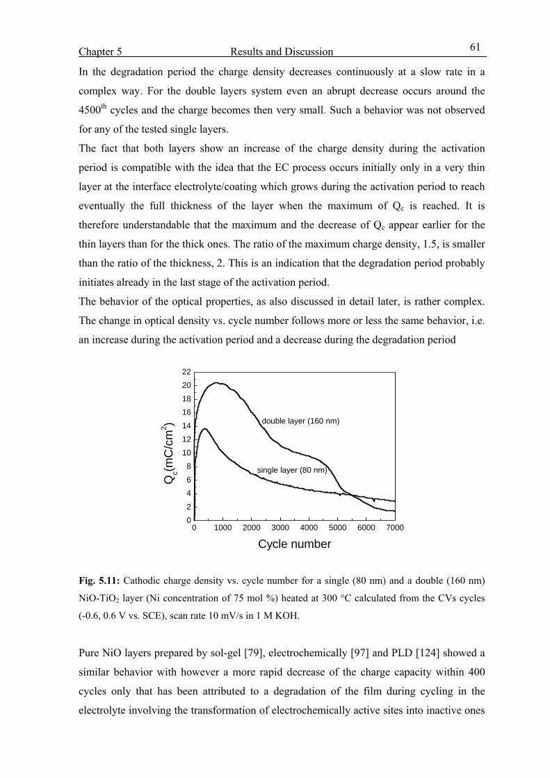
Chapter 5 Results and Discussion
61
In the degradation period the charge density decreases continuously at a slow rate in a
complex way. For the double layers system even an abrupt decrease occurs around the
4500th cycles and the charge becomes then very small. Such a behavior was not observed
for any of the tested single layers.
The fact that both layers show an increase of the charge density during the activation
period is compatible with the idea that the EC process occurs initially only in a very thin
layer at the interface electrolyte/coating which grows during the activation period to reach
eventually the full thickness of the layer when the maximum of Qc is reached. It is
therefore understandable that the maximum and the decrease of Qc appear earlier for the
thin layers than for the thick ones. The ratio of the maximum charge density, 1.5, is smaller
than the ratio of the thickness, 2. This is an indication that the degradation period probably
initiates already in the last stage of the activation period.
The behavior of the optical properties, as also discussed in detail later, is rather complex.
The change in optical density vs. cycle number follows more or less the same behavior, i.e.
an increase during the activation period and a decrease during the degradation period
0 1000 2000 3000 4000 5000 6000 70000
2
4
6
8
10
12
14
16
18
20
22
double layer (160 nm)
single layer (80 nm)
Qc(m
C/c
m2 )
Cycle number
Fig. 5.11: Cathodic charge density vs. cycle number for a single (80 nm) and a double (160 nm)
NiO-TiO2 layer (Ni concentration of 75 mol %) heated at 300 °C calculated from the CVs cycles
(-0.6, 0.6 V vs. SCE), scan rate 10 mV/s in 1 M KOH.
Pure NiO layers prepared by sol-gel [79], electrochemically [97] and PLD [124] showed a
similar behavior with however a more rapid decrease of the charge capacity within 400
cycles only that has been attributed to a degradation of the film during cycling in the
electrolyte involving the transformation of electrochemically active sites into inactive ones
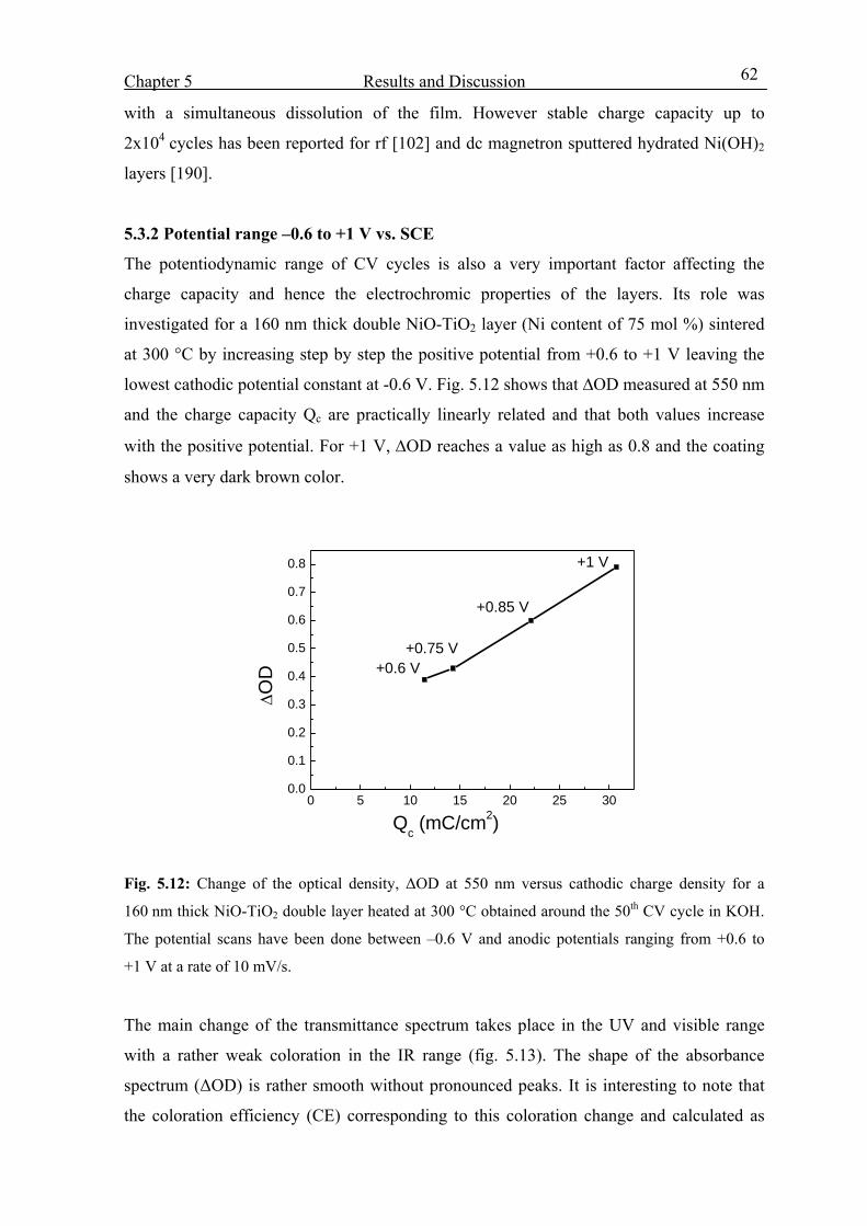
Chapter 5 Results and Discussion
62
with a simultaneous dissolution of the film. However stable charge capacity up to
2x10⁴ cycles has been reported for rf [102] and dc magnetron sputtered hydrated Ni(OH)2
layers [190].
5.3.2 Potential range –0.6 to +1 V vs. SCE
The potentiodynamic range of CV cycles is also a very important factor affecting the
charge capacity and hence the electrochromic properties of the layers. Its role was
investigated for a 160 nm thick double NiO-TiO2 layer (Ni content of 75 mol %) sintered
at 300 °C by increasing step by step the positive potential from +0.6 to +1 V leaving the
lowest cathodic potential constant at -0.6 V. Fig. 5.12 shows that ∆OD measured at 550 nm
and the charge capacity Qc are practically linearly related and that both values increase
with the positive potential. For +1 V, ΔOD reaches a value as high as 0.8 and the coating
shows a very dark brown color.
0 5 10 15 20 25 300.0
0.1
0.2
0.3
0.4
0.5
0.6
0.7
0.8 +1 V
+0.85 V
+0.75 V+0.6 V
ΔOD
Qc (mC/cm2)
Fig. 5.12: Change of the optical density, ΔOD at 550 nm versus cathodic charge density for a
160 nm thick NiO-TiO2 double layer heated at 300 °C obtained around the 50th CV cycle in KOH.
The potential scans have been done between –0.6 V and anodic potentials ranging from +0.6 to
+1 V at a rate of 10 mV/s.
The main change of the transmittance spectrum takes place in the UV and visible range
with a rather weak coloration in the IR range (fig. 5.13). The shape of the absorbance
spectrum (ΔOD) is rather smooth without pronounced peaks. It is interesting to note that
the coloration efficiency (CE) corresponding to this coloration change and calculated as
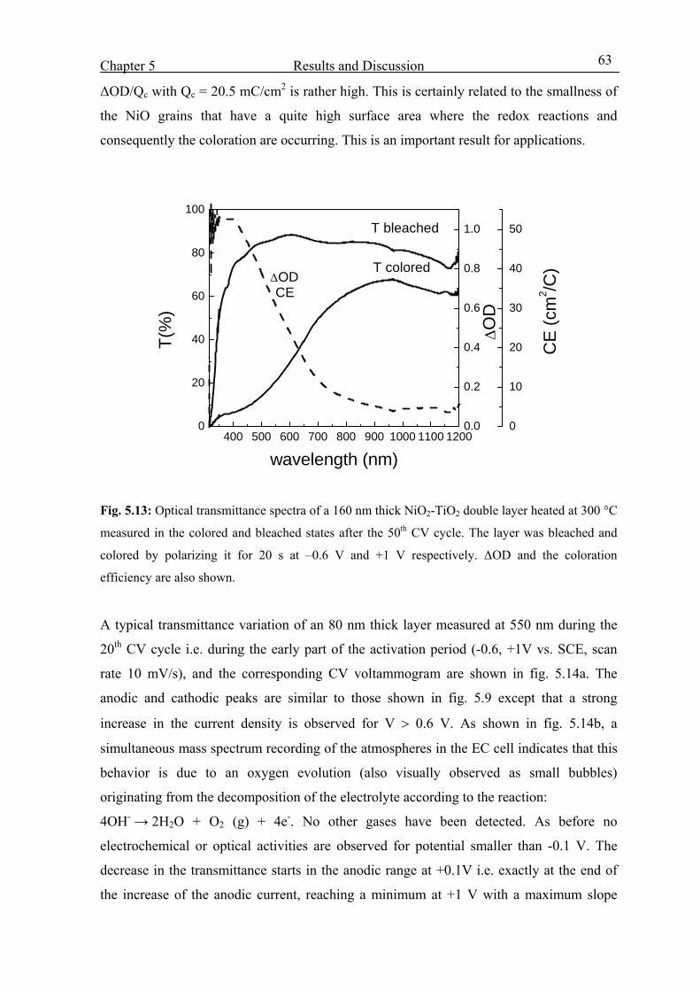
Chapter 5 Results and Discussion
63
ΔOD/Qc with Qc = 20.5 mC/cm2 is rather high. This is certainly related to the smallness of
the NiO grains that have a quite high surface area where the redox reactions and
consequently the coloration are occurring. This is an important result for applications.
400 500 600 700 800 900 1000 1100 12000
20
40
60
80
100
0.0
0.2
0.4
0.6
0.8
1.0
0
10
20
30
40
50
ΔOD
T colored
T bleached
T(%
)
wavelength (nm)
CEΔOD
CE
(cm
2 /C)
Fig. 5.13: Optical transmittance spectra of a 160 nm thick NiO2-TiO2 double layer heated at 300 °C
measured in the colored and bleached states after the 50th CV cycle. The layer was bleached and
colored by polarizing it for 20 s at –0.6 V and +1 V respectively. ΔOD and the coloration
efficiency are also shown.
A typical transmittance variation of an 80 nm thick layer measured at 550 nm during the
20th CV cycle i.e. during the early part of the activation period (-0.6, +1V vs. SCE, scan
rate 10 mV/s), and the corresponding CV voltammogram are shown in fig. 5.14a. The
anodic and cathodic peaks are similar to those shown in fig. 5.9 except that a strong
increase in the current density is observed for V > 0.6 V. As shown in fig. 5.14b, a
simultaneous mass spectrum recording of the atmospheres in the EC cell indicates that this
behavior is due to an oxygen evolution (also visually observed as small bubbles)
originating from the decomposition of the electrolyte according to the reaction:
4OH- → 2H2O + O2 (g) + 4e-. No other gases have been detected. As before no
electrochemical or optical activities are observed for potential smaller than -0.1 V. The
decrease in the transmittance starts in the anodic range at +0.1V i.e. exactly at the end of
the increase of the anodic current, reaching a minimum at +1 V with a maximum slope
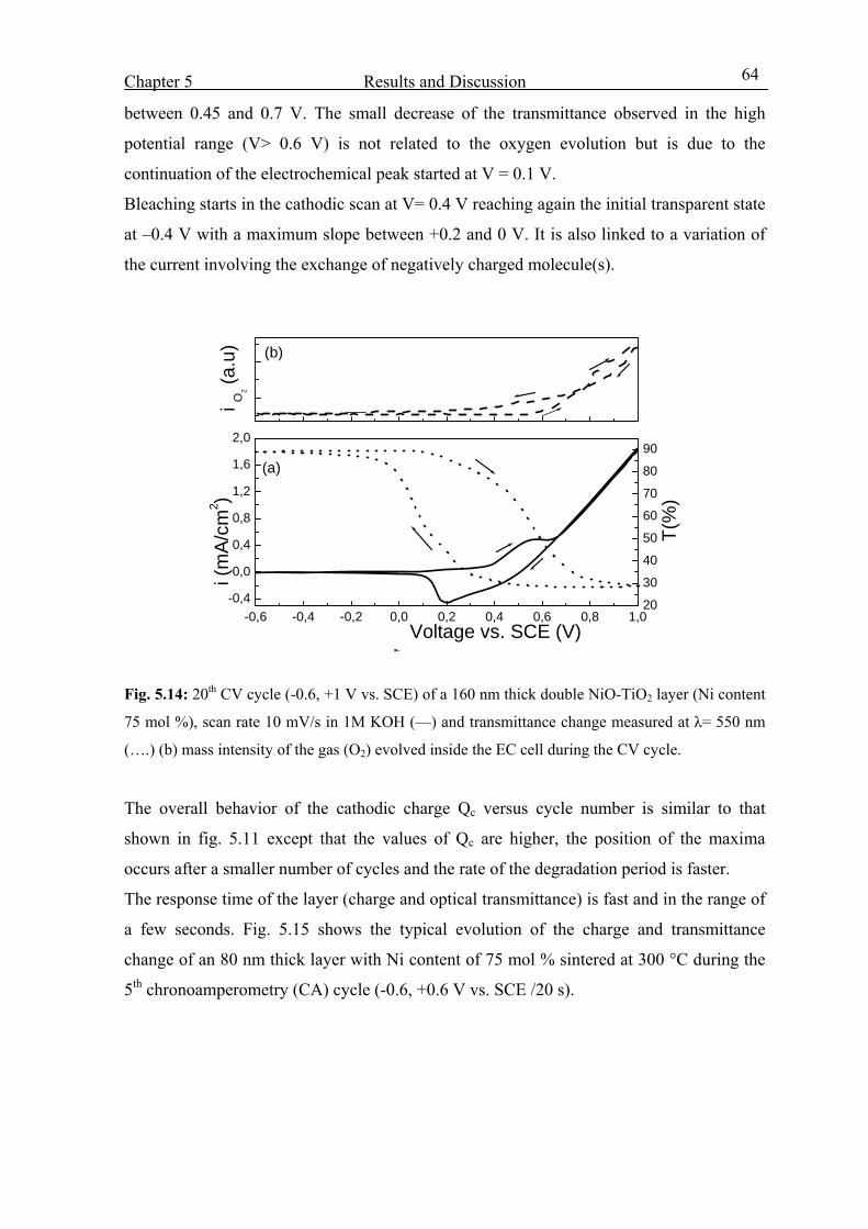
Chapter 5 Results and Discussion
64
between 0.45 and 0.7 V. The small decrease of the transmittance observed in the high
potential range (V> 0.6 V) is not related to the oxygen evolution but is due to the
continuation of the electrochemical peak started at V = 0.1 V.
Bleaching starts in the cathodic scan at V= 0.4 V reaching again the initial transparent state
at –0.4 V with a maximum slope between +0.2 and 0 V. It is also linked to a variation of
the current involving the exchange of negatively charged molecule(s).
-0,6 -0,4 -0,2 0,0 0,2 0,4 0,6 0,8 1,0-0,4
0,0
0,4
0,8
1,2
1,6
2,0
20
30
40
50
60
70
80
90(a)
T(%
)
Voltage vs. SCE (V)
i (m
A/cm
2 )i O
2 (a.u
) (b)
Fig. 5.14: 20th CV cycle (-0.6, +1 V vs. SCE) of a 160 nm thick double NiO-TiO2 layer (Ni content
75 mol %), scan rate 10 mV/s in 1M KOH (—) and transmittance change measured at λ= 550 nm
(….) (b) mass intensity of the gas (O2) evolved inside the EC cell during the CV cycle.
The overall behavior of the cathodic charge Qc versus cycle number is similar to that
shown in fig. 5.11 except that the values of Qc are higher, the position of the maxima
occurs after a smaller number of cycles and the rate of the degradation period is faster.
The response time of the layer (charge and optical transmittance) is fast and in the range of
a few seconds. Fig. 5.15 shows the typical evolution of the charge and transmittance
change of an 80 nm thick layer with Ni content of 75 mol % sintered at 300 °C during the
5th chronoamperometry (CA) cycle (-0.6, +0.6 V vs. SCE /20 s).
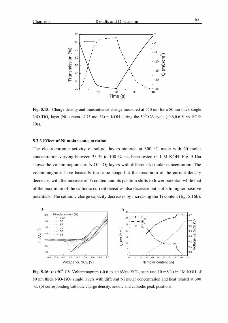
Chapter 5 Results and Discussion
65
0 10 20 30 40-25
-20
-15
-10
-5
0
5
20
30
40
50
60
70
80
90
Time (s)
Q (m
C/c
m2 )
Tran
smis
sion
(%)
Fig. 5.15: Charge density and transmittance change measured at 550 nm for a 80 nm thick single
NiO-TiO2 layer (Ni content of 75 mol %) in KOH during the 50th CA cycle (-0.6,0.6 V vs. SCE/
20s).
5.3.3 Effect of Ni molar concentration
The electrochromic activity of sol-gel layers sintered at 300 °C made with Ni molar
concentration varying between 33 % to 100 % has been tested in 1 M KOH. Fig. 5.16a
shows the voltammograms of NiO-TiO2 layers with different Ni molar concentration. The
voltammograms have basically the same shape but the maximum of the current density
decreases with the increase of Ti content and its position shifts to lower potential while that
of the maximum of the cathodic current densities also decrease but shifts to higher positive
potentials. The cathodic charge capacity decreases by increasing the Ti content (fig. 5.16b).
-0.6 -0.4 -0.2 0.0 0.2 0.4 0.6 0.8 1.0
-1.0
-0.5
0.0
0.5
1.0
1.5
2.0
a
Ni molar content (%) 100 90 87 75 50 33
i (m
A/cm
2 )
Voltage vs. SCE (V)0 10 20 30 40 50 60 70 80 90 100
0
5
10
15
20
25
30
35
0,0
0,1
0,2
0,3
0,4
0,5
0,6
0,7
Volta
ge v
s. S
CE
(V)
Qc
Qc (m
C/c
m2 )
Ni molar content (%)
b
Epa Epc
Fig. 5.16: (a) 50th CV Voltammogram (-0.6 to +0.6Vvs. SCE, scan rate 10 mV/s) in 1M KOH of
80 nm thick NiO-TiO2 single layers with different Ni molar concentration and heat treated at 300
°C, (b) corresponding cathodic charge density, anodic and cathodic peak positions.
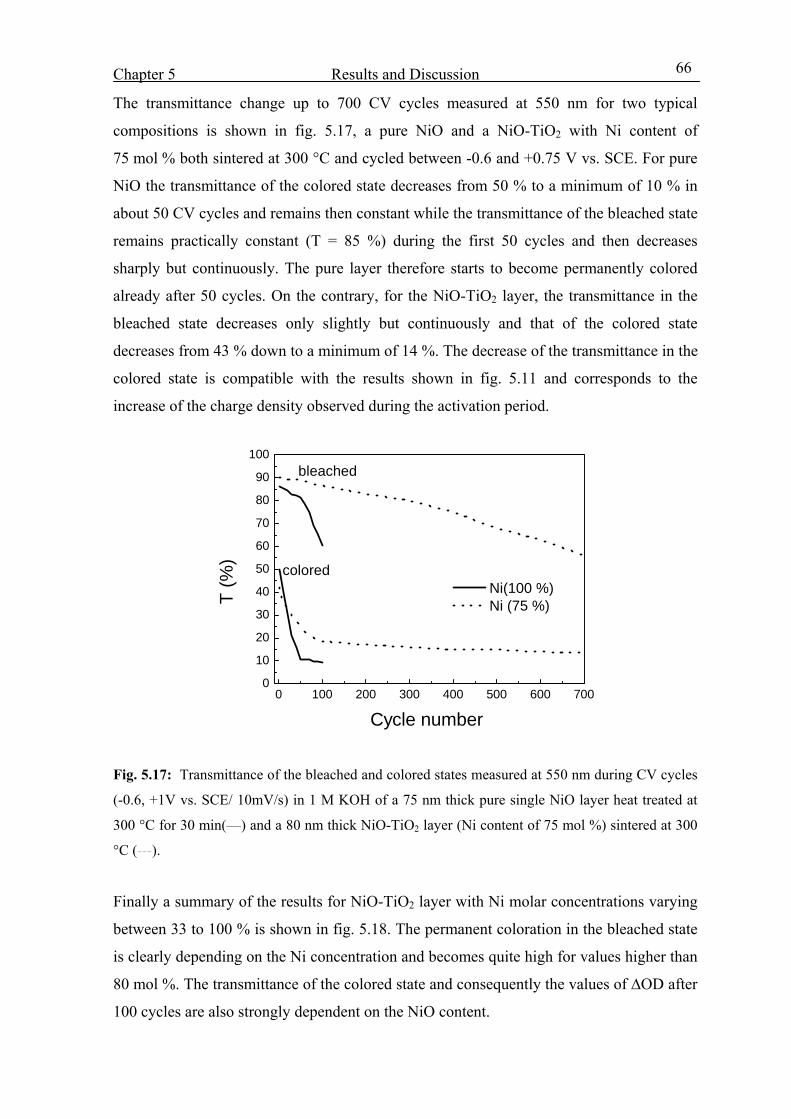
Chapter 5 Results and Discussion
66
The transmittance change up to 700 CV cycles measured at 550 nm for two typical
compositions is shown in fig. 5.17, a pure NiO and a NiO-TiO2 with Ni content of
75 mol % both sintered at 300 °C and cycled between -0.6 and +0.75 V vs. SCE. For pure
NiO the transmittance of the colored state decreases from 50 % to a minimum of 10 % in
about 50 CV cycles and remains then constant while the transmittance of the bleached state
remains practically constant (T = 85 %) during the first 50 cycles and then decreases
sharply but continuously. The pure layer therefore starts to become permanently colored
already after 50 cycles. On the contrary, for the NiO-TiO2 layer, the transmittance in the
bleached state decreases only slightly but continuously and that of the colored state
decreases from 43 % down to a minimum of 14 %. The decrease of the transmittance in the
colored state is compatible with the results shown in fig. 5.11 and corresponds to the
increase of the charge density observed during the activation period.
0 100 200 300 400 500 600 7000
10
20
30
40
50
60
70
80
90
100
colored
bleached
Ni(100 %) Ni (75 %)T
(%)
Cycle number
Fig. 5.17: Transmittance of the bleached and colored states measured at 550 nm during CV cycles
(-0.6, +1V vs. SCE/ 10mV/s) in 1 M KOH of a 75 nm thick pure single NiO layer heat treated at
300 °C for 30 min(—) and a 80 nm thick NiO-TiO2 layer (Ni content of 75 mol %) sintered at 300
°C (---).
Finally a summary of the results for NiO-TiO2 layer with Ni molar concentrations varying
between 33 to 100 % is shown in fig. 5.18. The permanent coloration in the bleached state
is clearly depending on the Ni concentration and becomes quite high for values higher than
80 mol %. The transmittance of the colored state and consequently the values of ∆OD after
100 cycles are also strongly dependent on the NiO content.
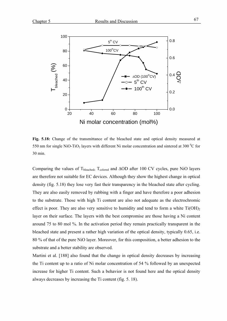
Chapter 5 Results and Discussion
67
0.0
0.2
0.4
0.6
0.8
20 40 60 80 1000
20
40
60
80
100
ΔOD ΔOD (100thCV)
100thCV
5th CV
5th CV 100th CVT bl
each
ed (%
)
Ni molar concentration (mol%)
Fig. 5.18: Change of the transmittance of the bleached state and optical density measured at
550 nm for single NiO-TiO2 layers with different Ni molar concentration and sintered at 300 0C for
30 min.
Comparing the values of Tbleached, Tcolored and ∆OD after 100 CV cycles, pure NiO layers
are therefore not suitable for EC devices. Although they show the highest change in optical
density (fig. 5.18) they lose very fast their transparency in the bleached state after cycling.
They are also easily removed by rubbing with a finger and have therefore a poor adhesion
to the substrate. Those with high Ti content are also not adequate as the electrochromic
effect is poor. They are also very sensitive to humidity and tend to form a white Ti(OH)2
layer on their surface. The layers with the best compromise are those having a Ni content
around 75 to 80 mol %. In the activation period they remain practically transparent in the
bleached state and present a rather high variation of the optical density, typically 0.65, i.e.
80 % of that of the pure NiO layer. Moreover, for this composition, a better adhesion to the
substrate and a better stability are observed.
Martini et al. [188] also found that the change in optical density decreases by increasing
the Ti content up to a ratio of Ni molar concentration of 54 % followed by an unexpected
increase for higher Ti content. Such a behavior is not found here and the optical density
always decreases by increasing the Ti content (fig. 5. 18).

Chapter 5 Results and Discussion
68
5.3.4 Effect of heat treatment
Dip-coated layers (75 mol % Ni content) were heated for 30 min at different temperatures
ranging from 250 to 500 °C and then cycled in 1M KOH electrolyte. Fig. 5.19a shows
typical CV curves measured during the 50th CV (-0.6, +0.6 V vs. SCE, scan rate 10 mV/s).
The overall behavior of the current density is similar but the large decrease of the
maximum value and a shift of its position is observed especially for sintering temperatures
T ≥ 350 °C. The change in optical density of the layers measured during the 1st and the
100th cycles (activation period) is shown in fig. 5.19b. The ΔOD values increase during the
activation period for all sintering temperatures but reach a constant high value only for
layers sintered up to 300 °C. The lower value obtained for the layers sintered at T ≥ 350 °C
may possibly be due to the better dehydration of the layers and indicates that the water
content and the hydration of the surface is an important factor to get a high electrochromic
activity [84].
Although the layers heated at T< 300 °C showed a large change of the optical density, they
gain a slight permanent coloration by cycling. On the contrary the layer sintered at 350 °C
shows the same change in optical density but its transmittance change in the bleached state
remains unaltered by cycling (T= 89 %) and is therefore the best compromise.
-0.6 -0.4 -0.2 0.0 0.2 0.4 0.6
-0.4
-0.2
0.0
0.2
0.4
0.6
a
250 °C 300 °C 350 °C 400 °C 500 °C
i (m
A/cm
2 )
Voltage vs. SCE(V)250 300 350 400 450 500
0.00
0.04
0.08
0.12
0.16
0.20
0.24
0.28
0.32b
1st CV
100th CV
ΔOD
Temperature (°C)
Fig. 5.19: 50th voltammogram (-0.6 to +0.6 V, scan rate 10mV/s) in 1M KOH of 80 nm thick NiO-
TiO2 single layers (Ni content 75 %) heat treated at different temperatures, (b) corresponding
change of the optical density measured at the wavelength of 550 nm during the 1st and 100th CV
cycles.
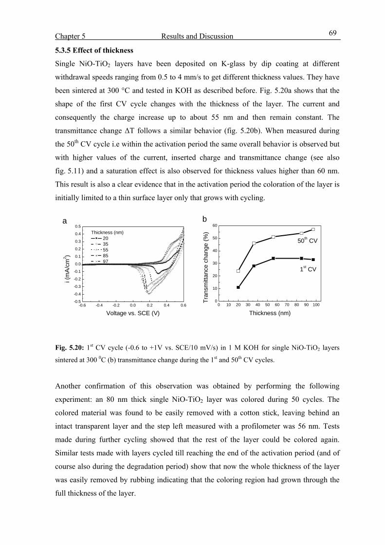
Chapter 5 Results and Discussion
69
5.3.5 Effect of thickness
Single NiO-TiO2 layers have been deposited on K-glass by dip coating at different
withdrawal speeds ranging from 0.5 to 4 mm/s to get different thickness values. They have
been sintered at 300 °C and tested in KOH as described before. Fig. 5.20a shows that the
shape of the first CV cycle changes with the thickness of the layer. The current and
consequently the charge increase up to about 55 nm and then remain constant. The
transmittance change ΔT follows a similar behavior (fig. 5.20b). When measured during
the 50th CV cycle i.e within the activation period the same overall behavior is observed but
with higher values of the current, inserted charge and transmittance change (see also
fig. 5.11) and a saturation effect is also observed for thickness values higher than 60 nm.
This result is also a clear evidence that in the activation period the coloration of the layer is
initially limited to a thin surface layer only that grows with cycling.
-0.6 -0.4 -0.2 0.0 0.2 0.4 0.6-0.5
-0.4
-0.3
-0.2
-0.1
0.0
0.1
0.2
0.3
0.4
0.5a
Thickness (nm) 20 35 55 85 97
i (m
A/cm
2 )
Voltage vs. SCE (V)0 10 20 30 40 50 60 70 80 90 100
0
10
20
30
40
50
60b
1st CV
50th CV
Tran
smitt
ance
cha
nge
(%)
Thickness (nm)
Fig. 5.20: 1st CV cycle (-0.6 to +1V vs. SCE/10 mV/s) in 1 M KOH for single NiO-TiO2 layers
sintered at 300 0C (b) transmittance change during the 1st and 50th CV cycles.
Another confirmation of this observation was obtained by performing the following
experiment: an 80 nm thick single NiO-TiO2 layer was colored during 50 cycles. The
colored material was found to be easily removed with a cotton stick, leaving behind an
intact transparent layer and the step left measured with a profilometer was 56 nm. Tests
made during further cycling showed that the rest of the layer could be colored again.
Similar tests made with layers cycled till reaching the end of the activation period (and of
course also during the degradation period) show that now the whole thickness of the layer
was easily removed by rubbing indicating that the coloring region had grown through the
full thickness of the layer.
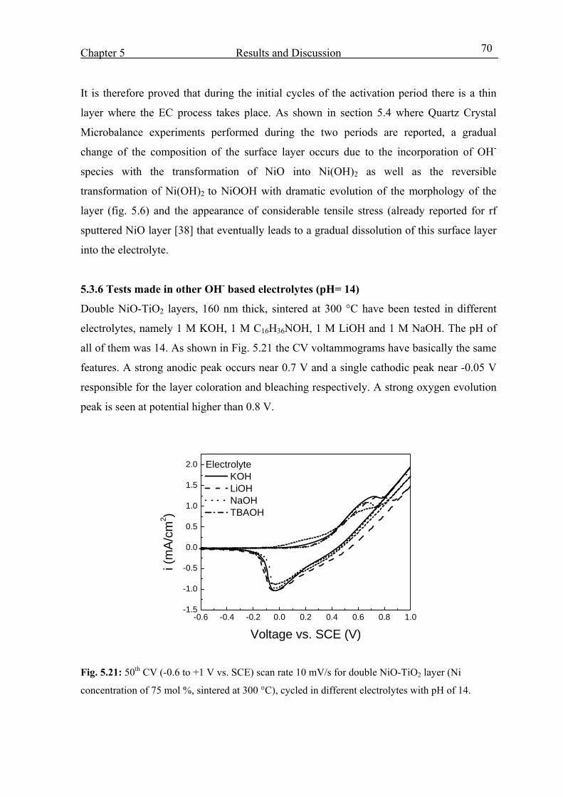
Chapter 5 Results and Discussion
70
It is therefore proved that during the initial cycles of the activation period there is a thin
layer where the EC process takes place. As shown in section 5.4 where Quartz Crystal
Microbalance experiments performed during the two periods are reported, a gradual
change of the composition of the surface layer occurs due to the incorporation of OH-
species with the transformation of NiO into Ni(OH)2 as well as the reversible
transformation of Ni(OH)2 to NiOOH with dramatic evolution of the morphology of the
layer (fig. 5.6) and the appearance of considerable tensile stress (already reported for rf
sputtered NiO layer [38] that eventually leads to a gradual dissolution of this surface layer
into the electrolyte.
5.3.6 Tests made in other OH- based electrolytes (pH= 14)
Double NiO-TiO2 layers, 160 nm thick, sintered at 300 °C have been tested in different
electrolytes, namely 1 M KOH, 1 M C16H36NOH, 1 M LiOH and 1 M NaOH. The pH of
all of them was 14. As shown in Fig. 5.21 the CV voltammograms have basically the same
features. A strong anodic peak occurs near 0.7 V and a single cathodic peak near -0.05 V
responsible for the layer coloration and bleaching respectively. A strong oxygen evolution
peak is seen at potential higher than 0.8 V.
-0.6 -0.4 -0.2 0.0 0.2 0.4 0.6 0.8 1.0-1.5
-1.0
-0.5
0.0
0.5
1.0
1.5
2.0
Electrolyte KOH LiOH NaOH TBAOH
i (m
A/cm
2 )
Voltage vs. SCE (V)
Fig. 5.21: 50th CV (-0.6 to +1 V vs. SCE) scan rate 10 mV/s for double NiO-TiO2 layer (Ni
concentration of 75 mol %, sintered at 300 °C), cycled in different electrolytes with pH of 14.
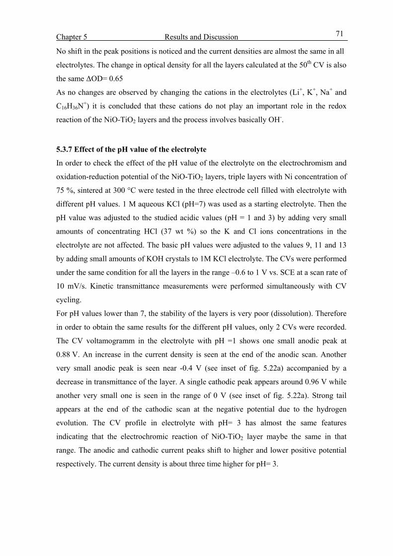
Chapter 5 Results and Discussion
71
No shift in the peak positions is noticed and the current densities are almost the same in all
electrolytes. The change in optical density for all the layers calculated at the 50th CV is also
the same ΔOD= 0.65
As no changes are observed by changing the cations in the electrolytes (Li+, K+, Na+ and
C16H36N+) it is concluded that these cations do not play an important role in the redox
reaction of the NiO-TiO2 layers and the process involves basically OH-.
5.3.7 Effect of the pH value of the electrolyte
In order to check the effect of the pH value of the electrolyte on the electrochromism and
oxidation-reduction potential of the NiO-TiO2 layers, triple layers with Ni concentration of
75 %, sintered at 300 °C were tested in the three electrode cell filled with electrolyte with
different pH values. 1 M aqueous KCl (pH=7) was used as a starting electrolyte. Then the
pH value was adjusted to the studied acidic values (pH = 1 and 3) by adding very small
amounts of concentrating HCl (37 wt %) so the K and Cl ions concentrations in the
electrolyte are not affected. The basic pH values were adjusted to the values 9, 11 and 13
by adding small amounts of KOH crystals to 1M KCl electrolyte. The CVs were performed
under the same condition for all the layers in the range –0.6 to 1 V vs. SCE at a scan rate of
10 mV/s. Kinetic transmittance measurements were performed simultaneously with CV
cycling.
For pH values lower than 7, the stability of the layers is very poor (dissolution). Therefore
in order to obtain the same results for the different pH values, only 2 CVs were recorded.
The CV voltamogramm in the electrolyte with pH =1 shows one small anodic peak at
0.88 V. An increase in the current density is seen at the end of the anodic scan. Another
very small anodic peak is seen near -0.4 V (see inset of fig. 5.22a) accompanied by a
decrease in transmittance of the layer. A single cathodic peak appears around 0.96 V while
another very small one is seen in the range of 0 V (see inset of fig. 5.22a). Strong tail
appears at the end of the cathodic scan at the negative potential due to the hydrogen
evolution. The CV profile in electrolyte with pH= 3 has almost the same features
indicating that the electrochromic reaction of NiO-TiO2 layer maybe the same in that
range. The anodic and cathodic current peaks shift to higher and lower positive potential
respectively. The current density is about three time higher for pH= 3.
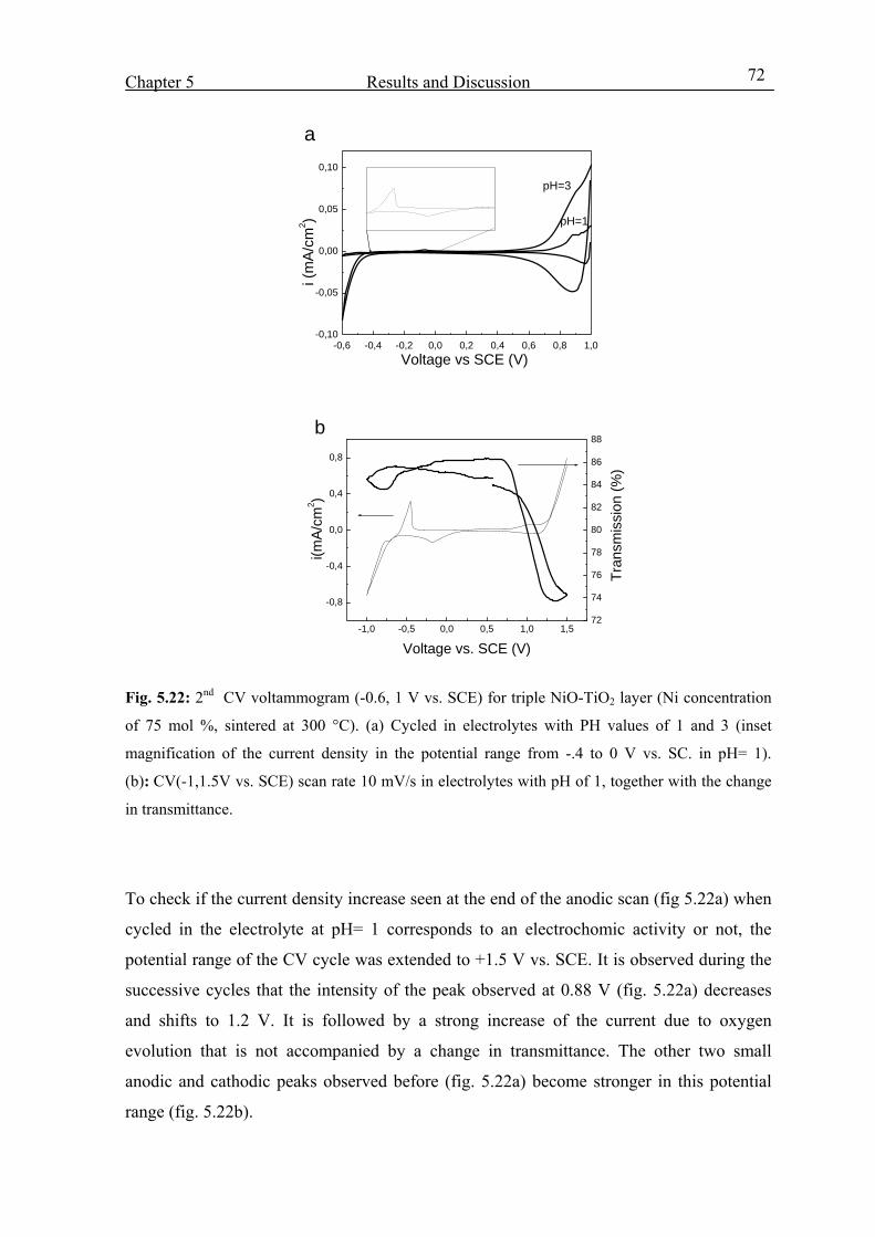
Chapter 5 Results and Discussion
72
-0,6 -0,4 -0,2 0,0 0,2 0,4 0,6 0,8 1,0-0,10
-0,05
0,00
0,05
0,10
a
pH=3
pH=1
i (m
A/cm
2 )
Voltage vs SCE (V)
-1,0 -0,5 0,0 0,5 1,0 1,5
-0,8
-0,4
0,0
0,4
0,8
72
74
76
78
80
82
84
86
88
Tran
smis
sion
(%)
i(mA/
cm2 )
Voltage vs. SCE (V)
b
Fig. 5.22: 2nd CV voltammogram (-0.6, 1 V vs. SCE) for triple NiO-TiO2 layer (Ni concentration
of 75 mol %, sintered at 300 °C). (a) Cycled in electrolytes with PH values of 1 and 3 (inset
magnification of the current density in the potential range from -.4 to 0 V vs. SC. in pH= 1).
(b): CV(-1,1.5V vs. SCE) scan rate 10 mV/s in electrolytes with pH of 1, together with the change
in transmittance.
To check if the current density increase seen at the end of the anodic scan (fig 5.22a) when
cycled in the electrolyte at pH= 1 corresponds to an electrochomic activity or not, the
potential range of the CV cycle was extended to +1.5 V vs. SCE. It is observed during the
successive cycles that the intensity of the peak observed at 0.88 V (fig. 5.22a) decreases
and shifts to 1.2 V. It is followed by a strong increase of the current due to oxygen
evolution that is not accompanied by a change in transmittance. The other two small
anodic and cathodic peaks observed before (fig. 5.22a) become stronger in this potential
range (fig. 5.22b).
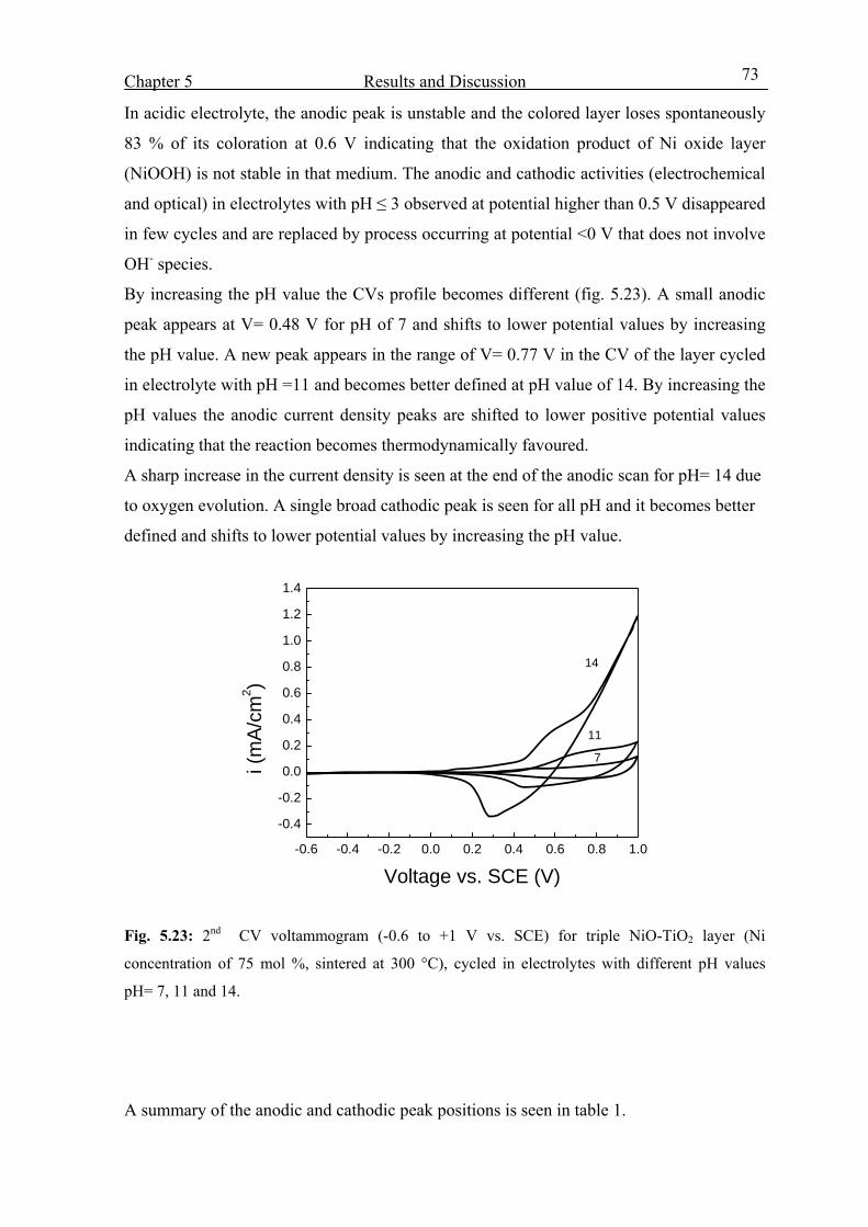
Chapter 5 Results and Discussion
73
In acidic electrolyte, the anodic peak is unstable and the colored layer loses spontaneously
83 % of its coloration at 0.6 V indicating that the oxidation product of Ni oxide layer
(NiOOH) is not stable in that medium. The anodic and cathodic activities (electrochemical
and optical) in electrolytes with pH ≤ 3 observed at potential higher than 0.5 V disappeared
in few cycles and are replaced by process occurring at potential <0 V that does not involve
OH- species.
By increasing the pH value the CVs profile becomes different (fig. 5.23). A small anodic
peak appears at V= 0.48 V for pH of 7 and shifts to lower potential values by increasing
the pH value. A new peak appears in the range of V= 0.77 V in the CV of the layer cycled
in electrolyte with pH =11 and becomes better defined at pH value of 14. By increasing the
pH values the anodic current density peaks are shifted to lower positive potential values
indicating that the reaction becomes thermodynamically favoured.
A sharp increase in the current density is seen at the end of the anodic scan for pH= 14 due
to oxygen evolution. A single broad cathodic peak is seen for all pH and it becomes better
defined and shifts to lower potential values by increasing the pH value.
-0.6 -0.4 -0.2 0.0 0.2 0.4 0.6 0.8 1.0
-0.4
-0.2
0.0
0.2
0.4
0.6
0.8
1.0
1.2
1.4
14
11
7
i (m
A/cm
2 )
Voltage vs. SCE (V)
Fig. 5.23: 2nd CV voltammogram (-0.6 to +1 V vs. SCE) for triple NiO-TiO2 layer (Ni
concentration of 75 mol %, sintered at 300 °C), cycled in electrolytes with different pH values
pH= 7, 11 and 14.
A summary of the anodic and cathodic peak positions is seen in table 1.
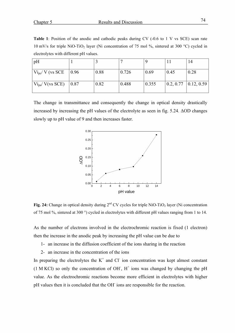
Chapter 5 Results and Discussion
74
Table 1: Position of the anodic and cathodic peaks during CV (-0.6 to 1 V vs SCE) scan rate
10 mV/s for triple NiO-TiO2 layer (Ni concentration of 75 mol %, sintered at 300 °C) cycled in
electrolytes with different pH values.
pH 1 3 7 9 11 14
Vipc/ V (vs SCE 0.96 0.88 0.726 0.69 0.45 0.28
Vipa/ V(vs SCE) 0.87 0.82 0.488 0.355 0.2, 0.77 0.12, 0.59
The change in transmittance and consequently the change in optical density drastically
increased by increasing the pH values of the electrolyte as seen in fig. 5.24. ΔOD changes
slowly up to pH value of 9 and then increases faster.
0 2 4 6 8 10 12 140.00
0.05
0.10
0.15
0.20
0.25
0.30
ΔOD
pH value
Fig. 24: Change in optical density during 2nd CV cycles for triple NiO-TiO2 layer (Ni concentration
of 75 mol %, sintered at 300 °) cycled in electrolytes with different pH values ranging from 1 to 14.
As the number of electrons involved in the electrochromic reaction is fixed (1 electron)
then the increase in the anodic peak by increasing the pH value can be due to
1- an increase in the diffusion coefficient of the ions sharing in the reaction
2- an increase in the concentration of the ions
In preparing the electrolytes the K+ and Cl- ion concentration was kept almost constant
(1 M KCl) so only the concentration of OH-, H+ ions was changed by changing the pH
value. As the electrochromic reactions become more efficient in electrolytes with higher
pH values then it is concluded that the OH- ions are responsible for the reaction.
Chapter 5 Results and Discussion
75
5.4 Coloration mechanism studied by EQCM 5.5.1 Introduction
The phenomenon of electrochromism in oxide electrodes is usually interpreted as an
electron transfer reaction that accompanies the insertion of electroactive species, such as
H+, OH- or Li+, into the amorphous or crystalline structure of host materials, resulting in
new absorption bands and an altered material coloration [205]. Understanding the
mechanism of ion insertion in metal oxides during an electrochromic reaction is therefore
central to clarify the optical performance but also the electrode failure. It is well known
that the detailed insertion mechanisms are usually highly complex and may consist of
several processes involving the diffusion of electrons and ions.
Electrochromic NiO-based coatings are among the least understood material and the
electrochemical mechanisms that lead to electrochromism are still controversial. In general
it is accepted that the coloration is due to the oxidation of Ni(II) into Ni(III) involving the
transformation of β-Ni(OH)2 into NiOOH. It is also well known that there is more than one
Ni(OH)2 phase. The most popular one is called β-Ni(OH)2 and can intercalate water to
form what is known as the α-Ni(OH)2 phase. The corresponding oxidized forms are
β-NiOOH and γ-NiOOH respectively. From the extended arguments found in the literature
for explaining the electrochromism of nickel-based oxides (see chapter 3) it can be
concluded that the mechanisms of coloration are strongly dependent on two main factors
(i) the composition and the phase of the starting nickel oxide layer, which in turn is
strongly dependent on the layer deposition technique and experimental
conditions
(ii) the kind of involved species during cycling. When a layer is tested in aqueous
basic solution for instance the most probable ones are H+, OH- or both. As will
be discussed in section 5.5 when an aprotic Li+ electrolyte is used, then Li+ will
be the most probable species.
Attempts have already been made to clarify the EC mechanisms using a combination of
different electrochemical and optical techniques [116, 190]. Among them, the
electrochemical quartz crystal microbalance (EQCM) technique has been used to address
the behavior of nickel-based oxides in alkaline solution in the field of battery [206, 207].
However, very few works have been reported aiming to understand the electrochromism of
this material [78, 201]. This technique is based on a quartz crystal microbalance (QCM)
that uses a piezoelectric crystal oscillating at a defined frequency and where small mass
changes on the crystal surface are detected by the shift of this frequency.

Chapter 5 Results and Discussion
76
Bernard et al.[206] studied the electrochemical kinetics of the ionic exchange process of
cathodically precipitated Ni(OH)2 in 5 M alkaline solution under a sinusoidal modulation
and concluded that the electrochemical reaction involves both the incorporation of
hydrated cations and a deprotonation according to the reaction
Ni(OH)2 + y M(H2O)x/y ↔ My Hz (NiO2)(H2O)x + (2-z) H+ + (2-z-y) e- (5.1)
The cations M can be Li+, Na+, K+, Rb+ or Cs+.
Based on this reaction, Cordoba-Torresi et al. [201] found that the coloration reaction of
electrochemically deposited Ni(OH)2 in a lower concentration alkaline electrolyte
(1 M KOH or LiOH) involves the incorporation of hydrated cations and that the number of
coordinated H2O molecules was depending on the kind of cations according to the reaction
Ni(OH)2 + y M(H2O) x/y + (2-z)OH-↔My Hz (NiO2)(H2O)x + (2-z) H2O + (2-z-y) e- (5.2)
Bange et al. [78] studied the coloration mechanism of e-beam evaporated Ni(OH)x films in
1 M NaOH and 1 M NaOD in the potential range –0.5 to +0.6 V vs. SCE. They divided the
coloration process (anodic range) into two main steps summarized by the following
equations
E< 0.32 V: Ni(OH)2 – H+ ↔ NiOOH + e- (5.3)
E> 0.32 V: Ni(OH)2 + 1/3OH- -2/3H+ ↔ NiOOH·1/3H2O + e- (5.4)
For E< 0.32 V only a hydrogen ejection occurs producing an electrochromic change in the
optical properties and a very small decrease in mass. For potential E> 0.32 V this process
is superimposed to an OH- injection.
The goal of the present work, therefore, was to investigate the mass change of NiO-TiO2
sol-gel layers, during cycling in KOH electrolyte using the EQCM technique in order to
get a better understanding of the mechanism of coloration of such nickel oxide-based
electrodes and hopefully to understand the role of the transformation of the different
phases on the stability and the degradation of these electrodes.
For this purpose double NiO-TiO2 layers were deposited on gold coated quartz crystal
substrate by the dip coating technique. The substrate was withdrawn from the precursor
solution at a rate of 3 mm/s in ambient atmosphere (RH<60 %). One side was covered to

Chapter 5 Results and Discussion
77
avoid the deposition of the layer on both sides. The system was then sintered at 300°C for
30 min. in air.
All electrochemical parameters (i, Q) could be of course determined using this
configuration. However the quartz crystal electrode being opaque, no determination of the
transmittance change could be measured and one has to rely on the results described in
fig. 5.9.
5.5.2 Envelope of the mass and charge change during 700 CV cycles
To estimate the mass of the layer, the frequency of gold coated quartz crystal was recorded
before and after the layer deposition. From the frequency shift due to the layer deposition
the mass of the deposited NiO-TiO2 with Ni:Ti molar ratio of 3:1 was 5.8 10-9g/cm2.
Assuming a density of NiO of 6.67 g/cm3 and that of TiO2= 4.25 g/cm3 the theoretical
value of the mass of the layer will be m= 0.75(6.67) + 0.25(4.25)160x10-7 i.e.
m= 9.66 10-9g/cm2. This indicates that the layer has a porosity of 40 %.
According to the recommendation of the balance manufacturer, the coated crystals were
left in the 1 M KOH electrolyte for four hours before starting the measurements. Then the
mass changes were first recorded at the open circuit potential (-0.11 V) for 47min. The
system was afterwards cycled by applying a potential in the range -0.4 to +0.57 V vs. SCE
at a scan rate of 10 mV/s.
Fig. 5.25 shows the results of the mass change at the open circuit potential and during the
first 5 CV cycles. The mass initially slightly increases linearly at a rate of about
7 ng/cm2/min, a value much smaller than the variation observed during the cycles. This is
thought to originate from a slow change in the composition of the layer due to a wetting
process occurring at the interface. However electronic artifact cannot be excluded.
-50 -40 -30 -20 -10 0 10 20-0.2
0.0
0.2
0.4
0.6
0.8
1.0
1.2
m (µ
g/cm
2 )
Time (min)
Fig. 5.25: Mass change at the open circuit potential (-0.11 V vs. SCE) during 47 min and then
during the first 5 CV cycles.
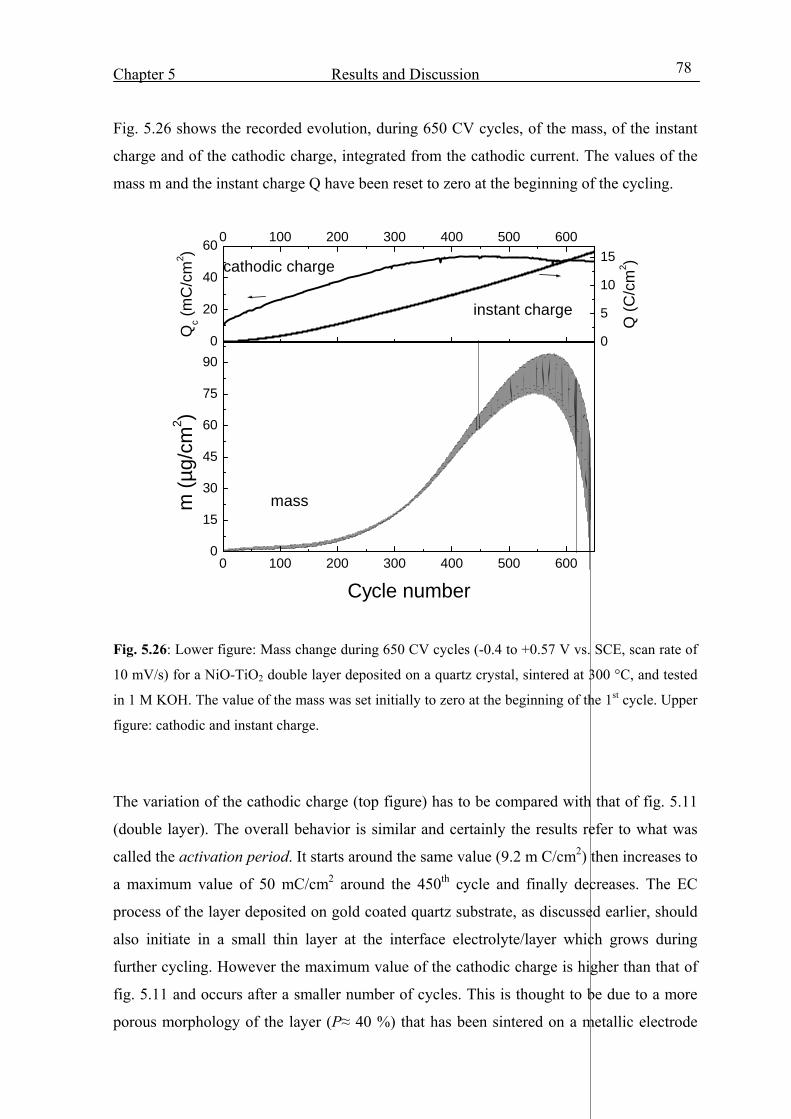
Chapter 5 Results and Discussion
78
Fig. 5.26 shows the recorded evolution, during 650 CV cycles, of the mass, of the instant
charge and of the cathodic charge, integrated from the cathodic current. The values of the
mass m and the instant charge Q have been reset to zero at the beginning of the cycling.
0 100 200 300 400 500 6000
15
30
45
60
75
900
20
40
600 100 200 300 400 500 600
0
5
10
15
mass
m (µ
g/cm
2 )
Cycle number
instant charge
cathodic charge
Qc (
mC
/cm
2 )
Q (C
/cm
2 )
Fig. 5.26: Lower figure: Mass change during 650 CV cycles (-0.4 to +0.57 V vs. SCE, scan rate of
10 mV/s) for a NiO-TiO2 double layer deposited on a quartz crystal, sintered at 300 °C, and tested
in 1 M KOH. The value of the mass was set initially to zero at the beginning of the 1st cycle. Upper
figure: cathodic and instant charge.
The variation of the cathodic charge (top figure) has to be compared with that of fig. 5.11
(double layer). The overall behavior is similar and certainly the results refer to what was
called the activation period. It starts around the same value (9.2 m C/cm2) then increases to
a maximum value of 50 mC/cm2 around the 450th cycle and finally decreases. The EC
process of the layer deposited on gold coated quartz substrate, as discussed earlier, should
also initiate in a small thin layer at the interface electrolyte/layer which grows during
further cycling. However the maximum value of the cathodic charge is higher than that of
fig. 5.11 and occurs after a smaller number of cycles. This is thought to be due to a more
porous morphology of the layer (P≈ 40 %) that has been sintered on a metallic electrode
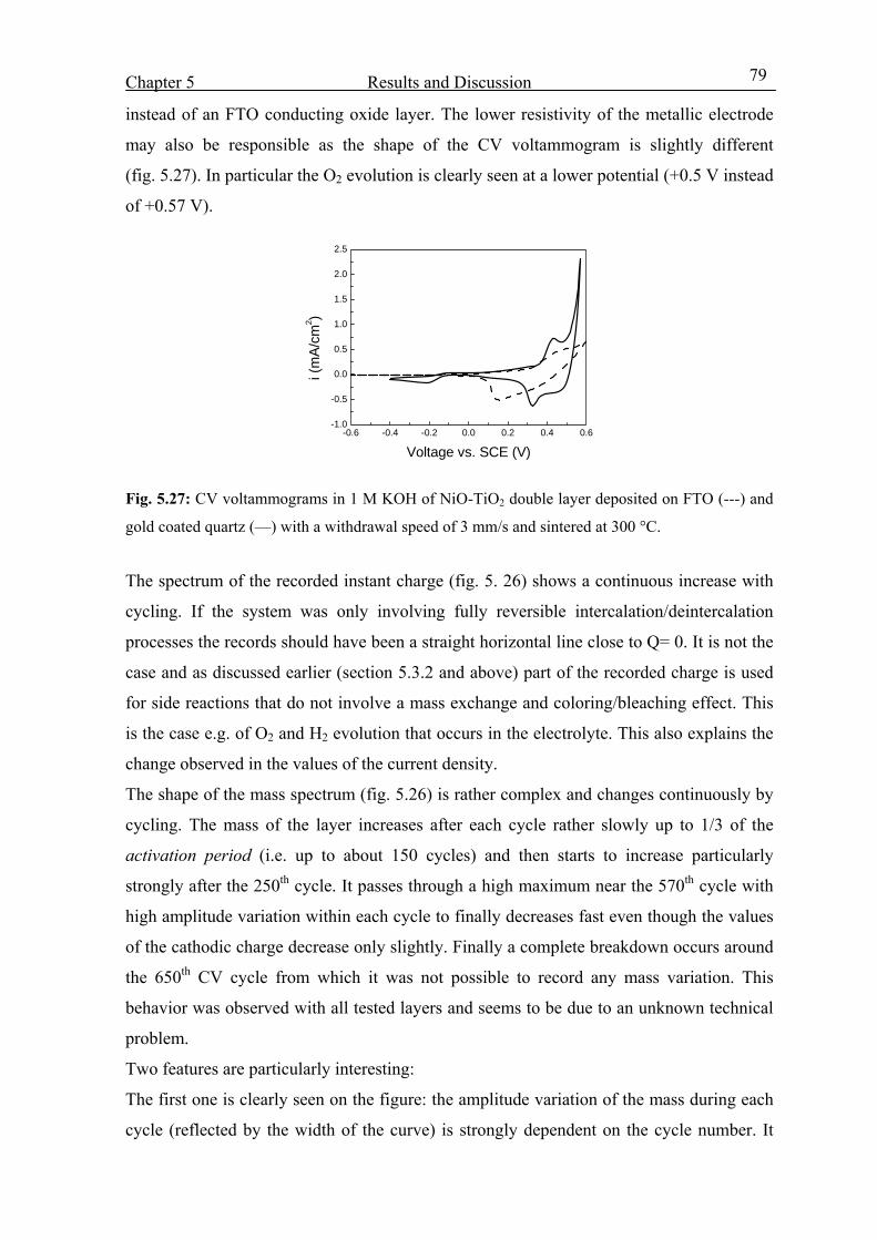
Chapter 5 Results and Discussion
79
instead of an FTO conducting oxide layer. The lower resistivity of the metallic electrode
may also be responsible as the shape of the CV voltammogram is slightly different
(fig. 5.27). In particular the O2 evolution is clearly seen at a lower potential (+0.5 V instead
of +0.57 V).
-0.6 -0.4 -0.2 0.0 0.2 0.4 0.6-1.0
-0.5
0.0
0.5
1.0
1.5
2.0
2.5
i (m
A/cm
2 )
Voltage vs. SCE (V)
Fig. 5.27: CV voltammograms in 1 M KOH of NiO-TiO2 double layer deposited on FTO (---) and
gold coated quartz (—) with a withdrawal speed of 3 mm/s and sintered at 300 °C.
The spectrum of the recorded instant charge (fig. 5. 26) shows a continuous increase with
cycling. If the system was only involving fully reversible intercalation/deintercalation
processes the records should have been a straight horizontal line close to Q= 0. It is not the
case and as discussed earlier (section 5.3.2 and above) part of the recorded charge is used
for side reactions that do not involve a mass exchange and coloring/bleaching effect. This
is the case e.g. of O2 and H2 evolution that occurs in the electrolyte. This also explains the
change observed in the values of the current density.
The shape of the mass spectrum (fig. 5.26) is rather complex and changes continuously by
cycling. The mass of the layer increases after each cycle rather slowly up to 1/3 of the
activation period (i.e. up to about 150 cycles) and then starts to increase particularly
strongly after the 250th cycle. It passes through a high maximum near the 570th cycle with
high amplitude variation within each cycle to finally decreases fast even though the values
of the cathodic charge decrease only slightly. Finally a complete breakdown occurs around
the 650th CV cycle from which it was not possible to record any mass variation. This
behavior was observed with all tested layers and seems to be due to an unknown technical
problem.
Two features are particularly interesting:
The first one is clearly seen on the figure: the amplitude variation of the mass during each
cycle (reflected by the width of the curve) is strongly dependent on the cycle number. It
Chapter 5 Results and Discussion
80
slowly increases from the 1st cycle up to about the 150th cycle, remains almost stable up to
200th cycle and then decreases to practically zero around the 330th cycle. Then it strongly
increases to reach values as high as 40 to 50 µg/cycle around the 600th cycle.
The second feature is observed by a closer look at these variations which shows that the
kinetics of the mass change during each cycle is also continuously changing. As reported
below the study was divided in several typical regions.
5.5.3 From the 1st to the 150th CV cycle
This period corresponds to about one third of the so-called activation period. Fig. 5.28a
shows the mass and charge changes during the first 5 CV cycles. Although the
measurements have been initiated at the open circuit potential (-0.11 V), for an easier
discussion, the results are presented initiating at the most negative potential (-0.4 V)
corresponding to the bleached state of the layer. The scan is performed in the direction of
positive potential (+0.57 V), and then it is scanned back to the negative potential. The
initial ordinate values for m and Q have been reset to zero. The lower figure shows the
results recorded between the 145th and 150th CV cycle.
The overall behavior of the mass and the charge in each cycle is similar. They increase in
the anodic range and decrease in the cathodic one so that the physical processes are
basically the same up to 150 cycles. However one observes that:
a- the change of the mass is 0.65 µg/cm2 during the first cycle and increases to a value
of 1.6 µg/cm2 during the 150th cycle (value then stable up to the 200th cycle)
b- the mass exchange is not fully reversible within each cycle so that the mass of the
layer increases continuously and linearly during cycling at a rate of about
30.4 ng/cm2/cycle. Taking into account the time required to perform the
measurement (194 s/cycle) this value corresponds to 9.4 ng/cm2/min i.e. a value
quite close to that observed at the open circuit (7.0 ng/cm2/min).
c- the peak height of the charge is 17 mC/cm2 during the 1st cycle and increases to
2.042 C/cm2 during the 150th cycle.
d- The charge is also not reversible and increases continuously but not linearly,
initially at a rate of 6.7 mC/cm2/cycle to reach a value of 20 mC/cm2/cycle during
the 150th cycle.
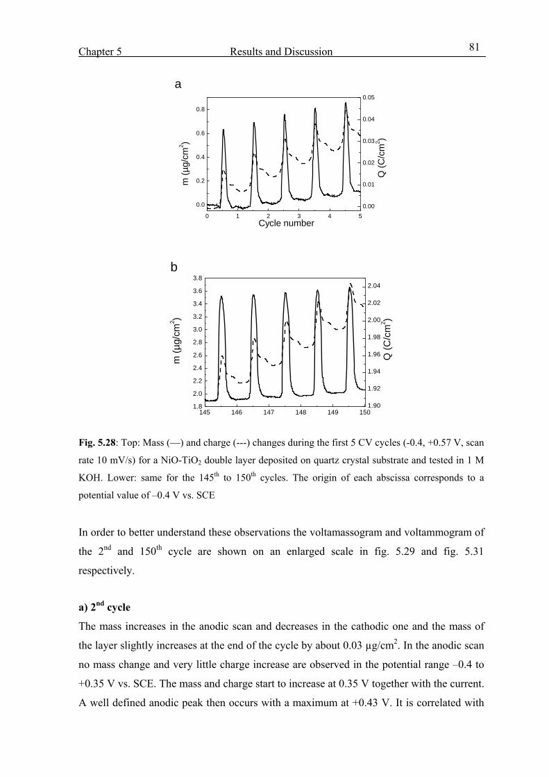
Chapter 5 Results and Discussion
81
0.0
0.2
0.4
0.6
0.8
0.00
0.01
0.02
0.03
0.04
0.05
0 1 2 3 4 5
m (µ
g/cm
2 )
a
Cycle number
Q (C
/cm
2 )
1.90
1.92
1.94
1.96
1.98
2.00
2.02
2.04
1.8
2.0
2.2
2.4
2.6
2.8
3.0
3.2
3.4
3.6
3.8
145 146 147 148 149 150
Q (C
/cm
2 )
m (µ
g/cm
2 )
b
Fig. 5.28: Top: Mass (—) and charge (---) changes during the first 5 CV cycles (-0.4, +0.57 V, scan
rate 10 mV/s) for a NiO-TiO2 double layer deposited on quartz crystal substrate and tested in 1 M
KOH. Lower: same for the 145th to 150th cycles. The origin of each abscissa corresponds to a
potential value of –0.4 V vs. SCE
In order to better understand these observations the voltamassogram and voltammogram of
the 2nd and 150th cycle are shown on an enlarged scale in fig. 5.29 and fig. 5.31
respectively.
a) 2nd cycle
The mass increases in the anodic scan and decreases in the cathodic one and the mass of
the layer slightly increases at the end of the cycle by about 0.03 µg/cm2. In the anodic scan
no mass change and very little charge increase are observed in the potential range –0.4 to
+0.35 V vs. SCE. The mass and charge start to increase at 0.35 V together with the current.
A well defined anodic peak then occurs with a maximum at +0.43 V. It is correlated with
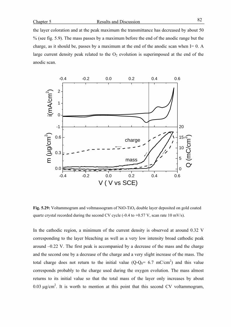
Chapter 5 Results and Discussion
82
the layer coloration and at the peak maximum the transmittance has decreased by about 50
% (see fig. 5.9). The mass passes by a maximum before the end of the anodic range but the
charge, as it should be, passes by a maximum at the end of the anodic scan when I= 0. A
large current density peak related to the O2 evolution is superimposed at the end of the
anodic scan.
-0.4 -0.2 0.0 0.2 0.4 0.6
0.0
0.3
0.6
-1
0
1
2
-0.4 -0.2 0.0 0.2 0.4 0.6
0
5
10
15
20
charge
mass
Q (m
C/c
m2 )
m (µ
g/cm
2 )
V ( V vs SCE)
i(mA/
cm2 )
Fig. 5.29: Voltammogram and voltmassogram of NiO-TiO2 double layer deposited on gold coated
quartz crystal recorded during the second CV cycle (-0.4 to +0.57 V, scan rate 10 mV/s).
In the cathodic region, a minimum of the current density is observed at around 0.32 V
corresponding to the layer bleaching as well as a very low intensity broad cathodic peak
around –0.22 V. The first peak is accompanied by a decrease of the mass and the charge
and the second one by a decrease of the charge and a very slight increase of the mass. The
total charge does not return to the initial value (Q-Q0= 6.7 mC/cm2) and this value
corresponds probably to the charge used during the oxygen evolution. The mass almost
returns to its initial value so that the total mass of the layer only increases by about
0.03 µg/cm2. It is worth to mention at this point that this second CV voltammogram,
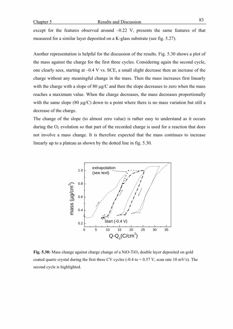
Chapter 5 Results and Discussion
83
except for the features observed around –0.22 V, presents the same features of that
measured for a similar layer deposited on a K-glass substrate (see fig. 5.27).
Another representation is helpful for the discussion of the results. Fig. 5.30 shows a plot of
the mass against the charge for the first three cycles. Considering again the second cycle,
one clearly sees, starting at –0.4 V vs. SCE, a small slight decrease then an increase of the
charge without any meaningful change in the mass. Then the mass increases first linearly
with the charge with a slope of 80 µg/C and then the slope decreases to zero when the mass
reaches a maximum value. When the charge decreases, the mass decreases proportionally
with the same slope (80 µg/C) down to a point where there is no mass variation but still a
decrease of the charge.
The change of the slope (to almost zero value) is rather easy to understand as it occurs
during the O2 evolution so that part of the recorded charge is used for a reaction that does
not involve a mass change. It is therefore expected that the mass continues to increase
linearly up to a plateau as shown by the dotted line in fig. 5.30.
0 5 10 15 20 25 30 35
0.2
0.4
0.6
0.8
1.0
mas
s (µ
g/cm
2 )
Q-Q0(C/cm2)
start (-0.4 V)
extrapolation(see text)
Fig. 5.30: Mass change against charge change of a NiO-TiO2 double layer deposited on gold
coated quartz crystal during the first three CV cycles (-0.4 to + 0.57 V, scan rate 10 mV/s). The
second cycle is highlighted.
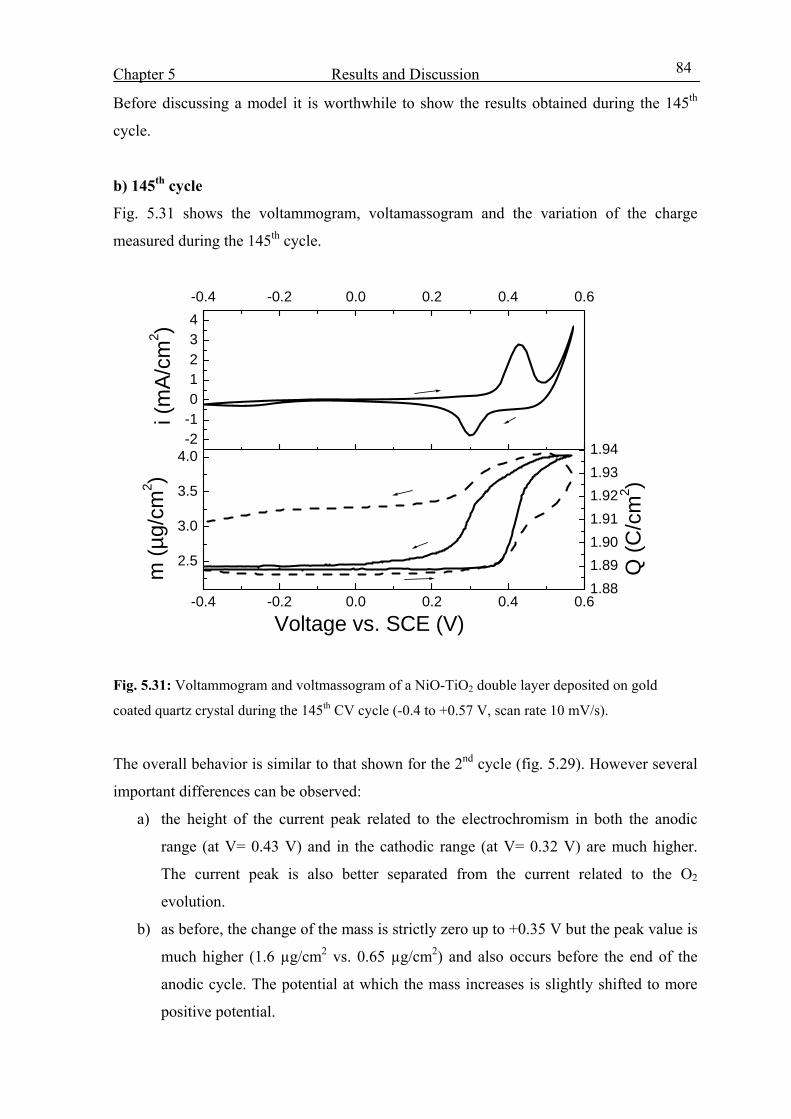
Chapter 5 Results and Discussion
84
Before discussing a model it is worthwhile to show the results obtained during the 145th
cycle.
b) 145th cycle
Fig. 5.31 shows the voltammogram, voltamassogram and the variation of the charge
measured during the 145th cycle.
2.5
3.0
3.5
4.0-2-101234-0.4 -0.2 0.0 0.2 0.4 0.6
-0.4 -0.2 0.0 0.2 0.4 0.61.881.891.901.911.921.931.94
m (µ
g/cm
2 )i (
mA/
cm2 )
Voltage vs. SCE (V)Q
(C/c
m2 )
Fig. 5.31: Voltammogram and voltmassogram of a NiO-TiO2 double layer deposited on gold
coated quartz crystal during the 145th CV cycle (-0.4 to +0.57 V, scan rate 10 mV/s).
The overall behavior is similar to that shown for the 2nd cycle (fig. 5.29). However several
important differences can be observed:
a) the height of the current peak related to the electrochromism in both the anodic
range (at V= 0.43 V) and in the cathodic range (at V= 0.32 V) are much higher.
The current peak is also better separated from the current related to the O2
evolution.
b) as before, the change of the mass is strictly zero up to +0.35 V but the peak value is
much higher (1.6 µg/cm2 vs. 0.65 µg/cm2) and also occurs before the end of the
anodic cycle. The potential at which the mass increases is slightly shifted to more
positive potential.
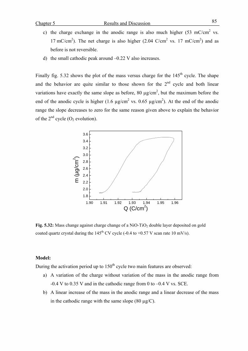
Chapter 5 Results and Discussion
85
c) the charge exchange in the anodic range is also much higher (53 mC/cm2 vs.
17 mC/cm2). The net charge is also higher (2.04 C/cm2 vs. 17 mC/cm2) and as
before is not reversible.
d) the small cathodic peak around –0.22 V also increases.
Finally fig. 5.32 shows the plot of the mass versus charge for the 145th cycle. The shape
and the behavior are quite similar to those shown for the 2nd cycle and both linear
variations have exactly the same slope as before, 80 µg/cm2, but the maximum before the
end of the anodic cycle is higher (1.6 µg/cm2 vs. 0.65 µg/cm2). At the end of the anodic
range the slope decreases to zero for the same reason given above to explain the behavior
of the 2nd cycle (O2 evolution).
1.90 1.91 1.92 1.93 1.94 1.95 1.96
1.8
2.0
2.2
2.4
2.6
2.8
3.0
3.2
3.4
3.6
m (µ
g/cm
2 )
Q (C/cm2)
Fig. 5.32: Mass change against charge change of a NiO-TiO2 double layer deposited on gold
coated quartz crystal during the 145th CV cycle (-0.4 to +0.57 V scan rate 10 mV/s).
Model:
During the activation period up to 150th cycle two main features are observed:
a) A variation of the charge without variation of the mass in the anodic range from
-0.4 V to 0.35 V and in the cathodic range from 0 to –0.4 V vs. SCE.
b) A linear increase of the mass in the anodic range and a linear decrease of the mass
in the cathodic range with the same slope (80 µg/C).
Chapter 5 Results and Discussion
86
The first feature is different from that observed by Bange et al.[78] for NiO layers
produced by e-beam evaporation where a small decrease of the mass was observed during
the first part of the anodic cycle explained as an evidence for a hydrogen ejection. For the
sol-gel layers there is no mass evolution in this range. Therefore the process observed only
as a small cathodic wave around –0.22 V should only involve reaction(s) with electrons.
The wave is however not seen in the voltammograms of layers deposited on FTO (see e.g.
fig.5.9) whatever is the potential range. Moreover, as it will be seen later, this wave will
become much more pronounced as cycling proceeds. The discussion of its origin will be
presented therefore later.
The second feature, the linear increase and decrease of the mass with the charge, is without
any doubt related to an almost fully reversible exchange of OH- groups that involves a
change of the oxidation state of Ni from 2+ to 3+ and vice versa (coloration and bleaching
respectively) at a lattice site.
The increase of the current density, charge and mass with cycling are compatible with the
ideas proposed earlier that, in this activation period, only a thin layer located at the
interface electrolyte/layer is active and that the thickness of this layer increases by cycling.
Without knowing with precision the complex surroundings of the NiO nanparticles, where
the presence of Ni(OH)2 (not observed by X-ray) and H2O too is expected because of the
low sintering temperature and/or by the wetting of the layer in the electrolyte, a precise
model can not be proposed. One possible equation to describe the results for E> 0.35 V is
xNi(OH)2 + xOH- ↔ (xNiOOH)·yH2O + (x-y) H2O+ xe- (5.5)
and dividing by x
Ni(OH)2 + OH- ↔ (NiOOH)·(y/x)H2O + (1-(y/x))H2O+ e- (5.6)
bleached colored
with 0 ≤ y≤ x
The x value is an arbitrary number greater than zero that describes the bonding of x
hydroxyl ion per Ni(OH)2 during the coloration of the film and the equation suggests the
formation of NiOOH and y/x lattice water bonded to NiOOH due to the incorporation of
OH- and the transfer of (1-y/x) water into the electrolyte.
According to this equation the change in mass of the sol-gel layer during the second cycle
will be
Mw = (y/x)MH2O-MH .(5.7)
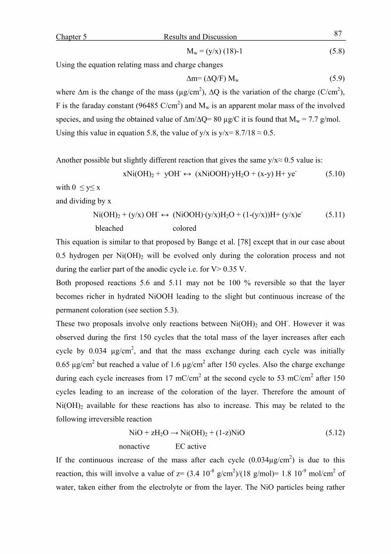
Chapter 5 Results and Discussion
87
Mw = (y/x) (18)-1 (5.8)
Using the equation relating mass and charge changes
∆m= (∆Q/F) Mw (5.9)
where ∆m is the change of the mass (µg/cm2), ∆Q is the variation of the charge (C/cm2),
F is the faraday constant (96485 C/cm2) and Mw is an apparent molar mass of the involved
species, and using the obtained value of ∆m/∆Q= 80 µg/C it is found that Mw = 7.7 g/mol.
Using this value in equation 5.8, the value of y/x is y/x= 8.7/18 ≈ 0.5.
Another possible but slightly different reaction that gives the same y/x≈ 0.5 value is:
xNi(OH)2 + yOH- ↔ (xNiOOH)·yH2O + (x-y) H+ ye- (5.10)
with 0 ≤ y≤ x
and dividing by x
Ni(OH)2 + (y/x) OH- ↔ (NiOOH)·(y/x)H2O + (1-(y/x))H+ (y/x)e- (5.11)
bleached colored
This equation is similar to that proposed by Bange et al. [78] except that in our case about
0.5 hydrogen per Ni(OH)2 will be evolved only during the coloration process and not
during the earlier part of the anodic cycle i.e. for V> 0.35 V.
Both proposed reactions 5.6 and 5.11 may not be 100 % reversible so that the layer
becomes richer in hydrated NiOOH leading to the slight but continuous increase of the
permanent coloration (see section 5.3).
These two proposals involve only reactions between Ni(OH)2 and OH-. However it was
observed during the first 150 cycles that the total mass of the layer increases after each
cycle by 0.034 µg/cm2, and that the mass exchange during each cycle was initially
0.65 µg/cm2 but reached a value of 1.6 µg/cm2 after 150 cycles. Also the charge exchange
during each cycle increases from 17 mC/cm2 at the second cycle to 53 mC/cm2 after 150
cycles leading to an increase of the coloration of the layer. Therefore the amount of
Ni(OH)2 available for these reactions has also to increase. This may be related to the
following irreversible reaction
NiO + zH2O → Ni(OH)2 + (1-z)NiO (5.12)
nonactive EC active
If the continuous increase of the mass after each cycle (0.034µg/cm2) is due to this
reaction, this will involve a value of z= (3.4 10-8 g/cm2)/(18 g/mol)= 1.8 10-9 mol/cm2 of
water, taken either from the electrolyte or from the layer. The NiO particles being rather
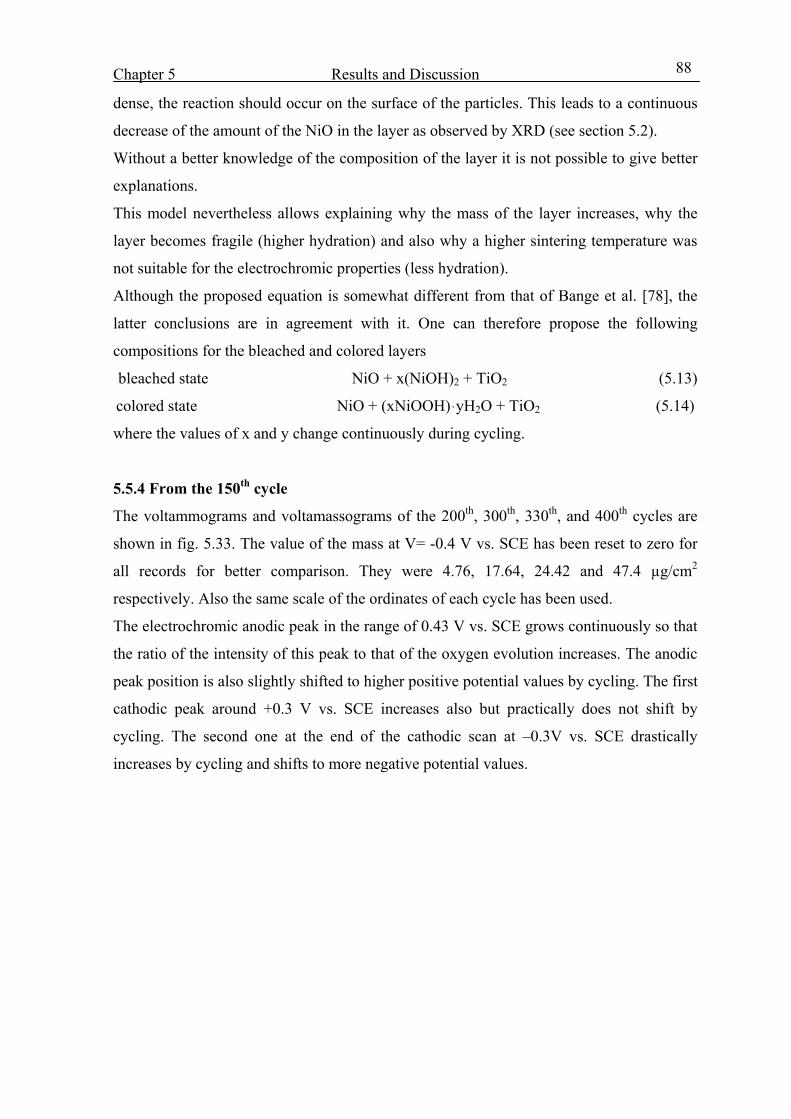
Chapter 5 Results and Discussion
88
dense, the reaction should occur on the surface of the particles. This leads to a continuous
decrease of the amount of the NiO in the layer as observed by XRD (see section 5.2).
Without a better knowledge of the composition of the layer it is not possible to give better
explanations.
This model nevertheless allows explaining why the mass of the layer increases, why the
layer becomes fragile (higher hydration) and also why a higher sintering temperature was
not suitable for the electrochromic properties (less hydration).
Although the proposed equation is somewhat different from that of Bange et al. [78], the
latter conclusions are in agreement with it. One can therefore propose the following
compositions for the bleached and colored layers
bleached state NiO + x(NiOH)2 + TiO2 (5.13)
colored state NiO + (xNiOOH)yH2O + TiO2 (5.14)
where the values of x and y change continuously during cycling.
5.5.4 From the 150th cycle
The voltammograms and voltamassograms of the 200th, 300th, 330th, and 400th cycles are
shown in fig. 5.33. The value of the mass at V= -0.4 V vs. SCE has been reset to zero for
all records for better comparison. They were 4.76, 17.64, 24.42 and 47.4 µg/cm2
respectively. Also the same scale of the ordinates of each cycle has been used.
The electrochromic anodic peak in the range of 0.43 V vs. SCE grows continuously so that
the ratio of the intensity of this peak to that of the oxygen evolution increases. The anodic
peak position is also slightly shifted to higher positive potential values by cycling. The first
cathodic peak around +0.3 V vs. SCE increases also but practically does not shift by
cycling. The second one at the end of the cathodic scan at –0.3V vs. SCE drastically
increases by cycling and shifts to more negative potential values.
Chapter 5 Results and Discussion
89
-0.4 -0.2 0.0 0.2 0.4 0.6-4-3-2-10123456789
i (m
A/cm
2 )
Voltage vs. SCE (V)
CV number 200 300 330 400
-0.4 -0.2 0.0 0.2 0.4 0.6
0.00.51.01.50.00.5
-0.50.0
-3
-2
-1
0
200th
m (µ
g/cm
2 )
V ( V vs SCE)
300th
330th
400th
Fig. 5.33: CV voltammograms and voltamassograms of the 200, 300, 330 and 400th CV cycles of
NiO-TiO2 double layer deposited on gold coated quartz crystal, sintered at 300 °C and tested in
1 M KOH in the potential range –0.4 to 0.57 V scan rate 10 mV/s. The ordinate scales of the mass
are the same in all graphs.
The shape of the voltamassogram during the 200th CV cycle (lower part of fig. 5.33) is
similar to that of the 150th cycle (see fig.5.31) and the mass increase occurs during the
anodic scan at a voltage corresponding to the anodic current peak. There are then however

Chapter 5 Results and Discussion
90
drastic changes between the 200th cycle and the 400th cycle. As before no mass change is
observed in the first part of the anodic cycle but the potential range slightly increases to
more positive values (from +0.4 V at the 200th cycle to +0.47 V at the 400th cycle).
The behavior at the end of the anodic cycle becomes rather complicated. The mass increase
is continuously reduced but it can still be observed up to about the 377th cycle. It is
substituted by a mass decrease around 0.48 V vs. SCE that can be observed already at the
300th cycle and that occurs in a very small potential range (0.48 to 0.52 V vs. SCE). At this
stage the absolute value of the mass change passes by a minimum (0.9 µg/cm2). Its value
then drastically increases with cycling to reach a value of 4 µg/cm2 at the 400th cycle. This
can be clearly observed by the width of the mass records in fig. 5.26.
At the end of the cathodic cycle a mass increase is now observed initiating at around
-0.22 V vs. SCE linked clearly to the increase of the height of the second cathodic current
peak. Its value grows with cycling to reach about 4 µg/cm2 at the 400th cycle. It should be
remembered that this cathodic peak was not observed by studying NiO-TiO2 layers
deposited on FTO conducting layer (see fig. 5.9).
The 330th cycle is found a good example for studying this transition period (fig. 5.34).
6.42
6.44
6.46
6.48
6.50-4-202468
10-0.4 -0.2 0.0 0.2 0.4 0.6
-0.4 -0.2 0.0 0.2 0.4 0.623.623.824.024.224.424.624.8
i(mA/
cm2 )
m (µ
g/cm
2 )
Q (C
/cm
2 )
Voltage vs. SCE (V)
Fig. 5.34: Voltammogram and voltmassogram for a NiO-TiO2 double layer deposited on gold
coated quartz crystal during the 330th CV cycle (-0.4, 0.57 V, scan rate 10 mV/s).
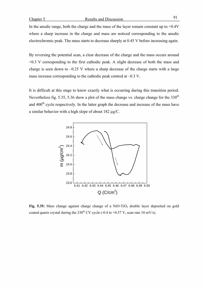
Chapter 5 Results and Discussion
91
In the anodic range, both the charge and the mass of the layer remain constant up to +0.4V
where a sharp increase in the charge and mass are noticed corresponding to the anodic
electrochromic peak. The mass starts to decrease sharply at 0.45 V before increasing again.
By reversing the potential scan, a clear decrease of the charge and the mass occurs around
+0.3 V corresponding to the first cathodic peak. A slight decrease of both the mass and
charge is seen down to –0.25 V where a sharp decrease of the charge starts with a large
mass increase corresponding to the cathodic peak centred at –0.3 V.
It is difficult at this stage to know exactly what is occurring during this transition period.
Nevertheless fig. 5.35, 5.36 show a plot of the mass change vs. charge change for the 330th
and 400th cycle respectively. In the latter graph the decrease and increase of the mass have
a similar behavior with a high slope of about 182 µg/C.
6.41 6.42 6.43 6.44 6.45 6.46 6.47 6.48 6.49 6.5023.6
23.8
24.0
24.2
24.4
24.6
24.8
m (µ
g/cm
2 )
Q (C/cm2)
Fig. 5.35: Mass change against charge change of a NiO-TiO2 double layer deposited on gold
coated quartz crystal during the 330th CV cycle (-0.4 to +0.57 V, scan rate 10 mV/s).
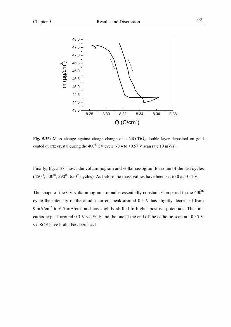
Chapter 5 Results and Discussion
92
8.28 8.30 8.32 8.34 8.36 8.3843.5
44.0
44.5
45.0
45.5
46.0
46.5
47.0
47.5
48.0
m (µ
g/cm
2 )
Q (C/cm2)
Fig. 5.36: Mass change against charge change of a NiO-TiO2 double layer deposited on gold
coated quartz crystal during the 400th CV cycle (-0.4 to +0.57 V scan rate 10 mV/s).
Finally, fig. 5.37 shows the voltammogram and voltamassogram for some of the last cycles
(450th, 500th, 590th, 650th cycles). As before the mass values have been set to 0 at –0.4 V.
The shape of the CV voltammograms remains essentially constant. Compared to the 400th
cycle the intensity of the anodic current peak around 0.5 V has slightly decreased from
9 mA/cm2 to 6.5 mA/cm2 and has slightly shifted to higher positive potentials. The first
cathodic peak around 0.3 V vs. SCE and the one at the end of the cathodic scan at –0.35 V
vs. SCE have both also decreased.
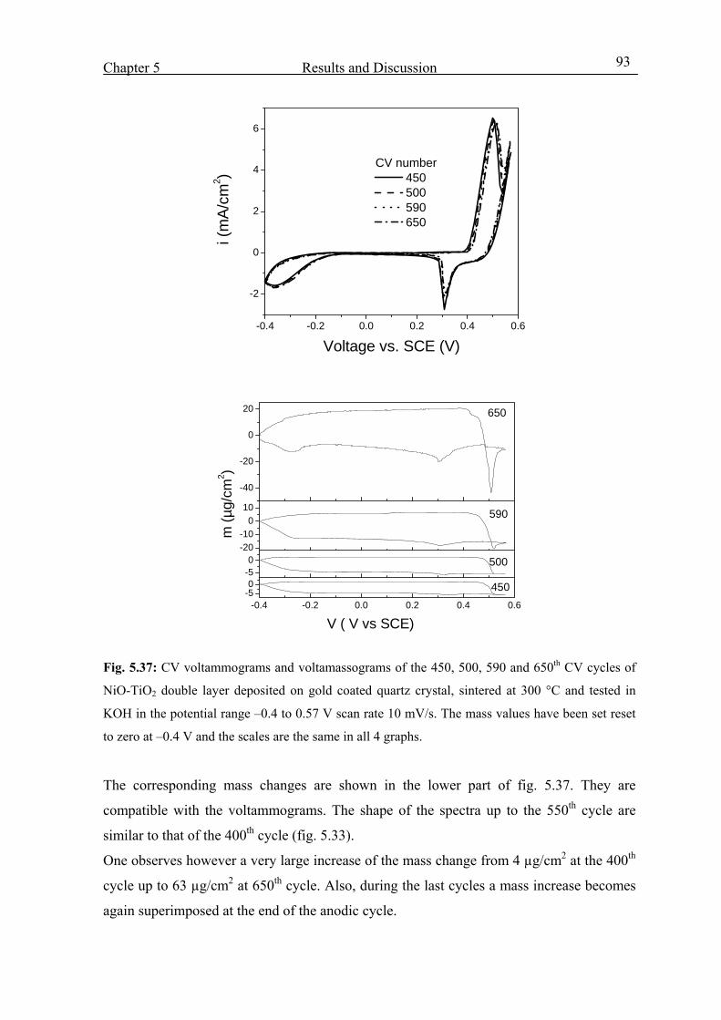
Chapter 5 Results and Discussion
93
-0.4 -0.2 0.0 0.2 0.4 0.6
-2
0
2
4
6
i (m
A/cm
2 )
Voltage vs. SCE (V)
CV number 450 500 590 650
-0.4 -0.2 0.0 0.2 0.4 0.6-50
-50
-20-10
010
-40
-20
0
20
V ( V vs SCE)
m (µ
g/cm
2 )
450
500
590
650
Fig. 5.37: CV voltammograms and voltamassograms of the 450, 500, 590 and 650th CV cycles of
NiO-TiO2 double layer deposited on gold coated quartz crystal, sintered at 300 °C and tested in
KOH in the potential range –0.4 to 0.57 V scan rate 10 mV/s. The mass values have been set reset
to zero at –0.4 V and the scales are the same in all 4 graphs.
The corresponding mass changes are shown in the lower part of fig. 5.37. They are
compatible with the voltammograms. The shape of the spectra up to the 550th cycle are
similar to that of the 400th cycle (fig. 5.33).
One observes however a very large increase of the mass change from 4 µg/cm2 at the 400th
cycle up to 63 µg/cm2 at 650th cycle. Also, during the last cycles a mass increase becomes
again superimposed at the end of the anodic cycle.
Chapter 5 Results and Discussion
94
As the cathodic peak at the end of the cathodic scan shift to more negative potentials, the
corresponding mass increase shifts in the same direction so that is only completed in the
anodic scan.
The results obtained till the 150th cycle have been correlated to the exchange of OH- during
the CV cycles that reacts with Ni(OH)2 to produce hydrated NiOOH (responsible for the
coloration of the layer), as well as intercalated water that reacts with NiO to increase the
amount of Ni(OH)2 in the layer to explain the increase of ∆OD and the decrease of the size
of the NiO nanoparticles by cycling. These changes in the layer composition associated by
an increase of the porosity and fragility. From 330th cycle one observes a drastic change of
the mass spectra that can only be explained by a partly irreversible exchange of positives
ions, these can only be K+ or hydrated K(H2O)n+ ions. The primary hydration umber of K
is 4 [208]. A similar behavior has been recently observed by Sun [144] for
(CeO2)0.81(TiO2)1 sol-gel counter electrode layer in wet LiClO4-PC electrolyte. The high
weight of the ions explains why the ratio of mass/charge obtained (e.g. from fig. 5.36 for
the 400th cycle) becomes higher (181 µg/C vs. 80 µg/C), why the total mass increases after
each cycle drastically up to 570 cycles. The layer morphology and structure become
therefore very loose up to a point (650th cycle) it breaks down and is dissolved in the
electrolyte.

Chapter 5 Results and Discussion
95
5.5 NiO-TiO2 layer characterization in LiClO4-PC electrolyte Scrosati et al. [143, 191, 192, 209] have studied the electrochromic behavior of dc
magnetron sputtered NiOx layer in aprotic LiClO4-PC electrolyte. It was shown that Li+
could be intercalated via two different steps leading to interesting coloring/bleaching
behavior especially useful for the development of WO3/electrolyte/NiO EC cells.
This section describes the results obtained with sol-gel NiO-TiO2 layers tested in the three
electrode cell filled with LiClO4-PC using Ag/AgClO4-PC as reference electrode. The
results are rather complex as they were found to be strongly dependent on the kinetics of
the process. Therefore the presentation is not exhaustive. For sake of clarity, the section
has been divided in 3 parts according to the potential range. Except for the spectrum, the
transmittance has been normalized considering the value in the bleached state as 100%.
a) potential range –1 to +1 V vs. Ag/AgClO4-PC
Studies for NiO based layers in a Li+ aprotic electrolyte in the potential range –0.5 to +1 V
vs. Ag/AgClO4-PC have not been reported.
Fig. 5.38 shows a galvanostatic coloration of a fresh uncolored NiO-TiO2 layer, 80 nm
thick sintered at 300 °C performed by applying a small positive current density of
+5µA/cm2. The potential increases continuously from 0 to +1.05 V and a small decrease of
the layer transmittance is observed (T/Tb decreases from 100 % to about 87 %) after
having incorporating a charge of 7 mC/cm2.
0 1 2 3 4 5 6 7
-0.2
0.0
0.2
0.4
0.6
0.8
1.0
1.2
0
86
88
90
92
94
96
98
100
Volta
ge v
s. A
g/Ag
ClO
4 (v)
Q (mC/cm2)
T/T bl
each
ed (%
)
Fig. 5.38. Potential and transmittance (550 nm) evolution of an 80 nm thick single NiO-TiO2 layer
(Ni content of 75 mol %) in LiClO4-PC during galvanostatic measurement using a positive current
density of +5µA/cm2.
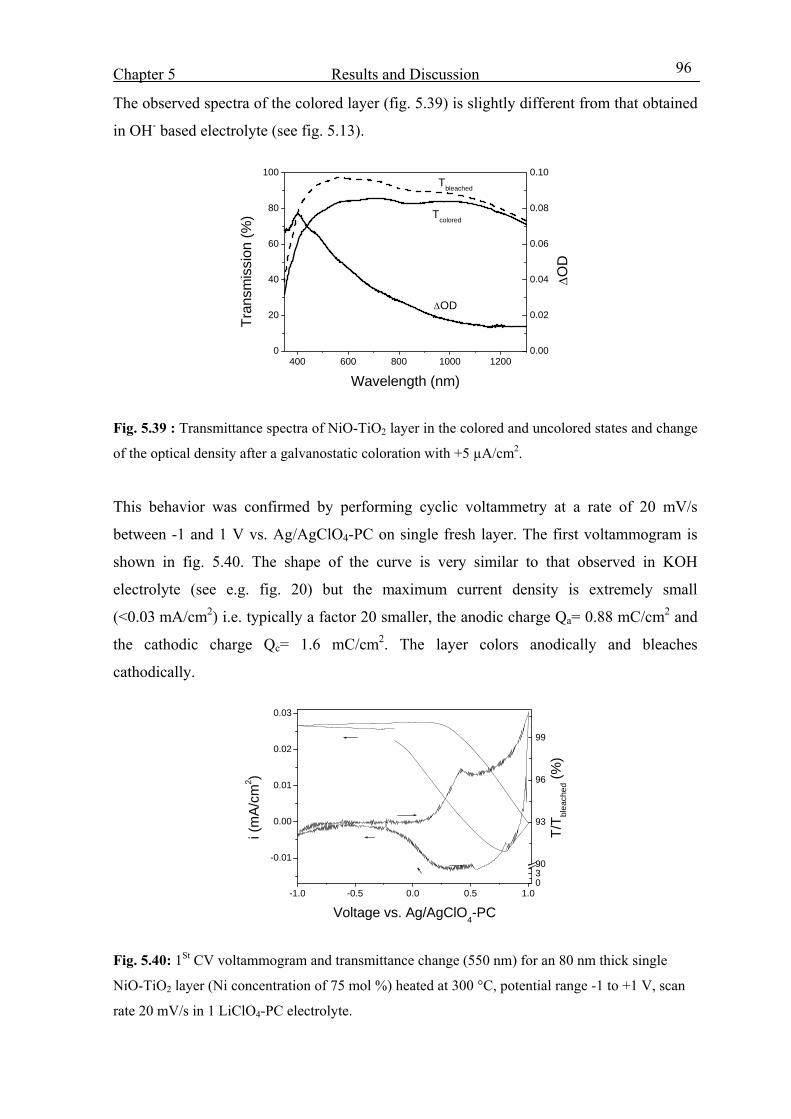
Chapter 5 Results and Discussion
96
The observed spectra of the colored layer (fig. 5.39) is slightly different from that obtained
in OH- based electrolyte (see fig. 5.13).
400 600 800 1000 12000
20
40
60
80
100
0.00
0.02
0.04
0.06
0.08
0.10
Tcolored
Tbleached
Tran
smis
sion
(%)
Wavelength (nm)
ΔOD
ΔOD
Fig. 5.39 : Transmittance spectra of NiO-TiO2 layer in the colored and uncolored states and change
of the optical density after a galvanostatic coloration with +5 µA/cm2.
This behavior was confirmed by performing cyclic voltammetry at a rate of 20 mV/s
between -1 and 1 V vs. Ag/AgClO4-PC on single fresh layer. The first voltammogram is
shown in fig. 5.40. The shape of the curve is very similar to that observed in KOH
electrolyte (see e.g. fig. 20) but the maximum current density is extremely small
(<0.03 mA/cm2) i.e. typically a factor 20 smaller, the anodic charge Qa= 0.88 mC/cm2 and
the cathodic charge Qc= 1.6 mC/cm2. The layer colors anodically and bleaches
cathodically.
0390
93
96
99
-1.0 -0.5 0.0 0.5 1.0
-0.01
0.00
0.01
0.02
0.03
T/T bl
each
ed (%
)
i (m
A/cm
2 )
Voltage vs. Ag/AgClO4-PC
Fig. 5.40: 1St CV voltammogram and transmittance change (550 nm) for an 80 nm thick single
NiO-TiO2 layer (Ni concentration of 75 mol %) heated at 300 °C, potential range -1 to +1 V, scan
rate 20 mV/s in 1 LiClO4-PC electrolyte.
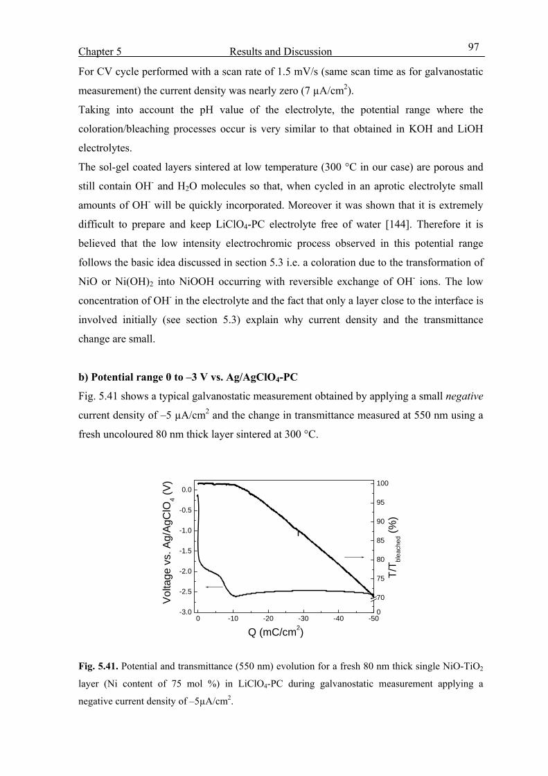
Chapter 5 Results and Discussion
97
For CV cycle performed with a scan rate of 1.5 mV/s (same scan time as for galvanostatic
measurement) the current density was nearly zero (7 µA/cm2).
Taking into account the pH value of the electrolyte, the potential range where the
coloration/bleaching processes occur is very similar to that obtained in KOH and LiOH
electrolytes.
The sol-gel coated layers sintered at low temperature (300 °C in our case) are porous and
still contain OH- and H2O molecules so that, when cycled in an aprotic electrolyte small
amounts of OH- will be quickly incorporated. Moreover it was shown that it is extremely
difficult to prepare and keep LiClO4-PC electrolyte free of water [144]. Therefore it is
believed that the low intensity electrochromic process observed in this potential range
follows the basic idea discussed in section 5.3 i.e. a coloration due to the transformation of
NiO or Ni(OH)2 into NiOOH occurring with reversible exchange of OH- ions. The low
concentration of OH- in the electrolyte and the fact that only a layer close to the interface is
involved initially (see section 5.3) explain why current density and the transmittance
change are small.
b) Potential range 0 to –3 V vs. Ag/AgClO4-PC
Fig. 5.41 shows a typical galvanostatic measurement obtained by applying a small negative
current density of –5 µA/cm2 and the change in transmittance measured at 550 nm using a
fresh uncoloured 80 nm thick layer sintered at 300 °C.
0 -10 -20 -30 -40 -50-3.0
-2.5
-2.0
-1.5
-1.0
-0.5
0.0
0
70
75
80
85
90
95
100
Volta
ge v
s. A
g/Ag
ClO
4 (V)
Q (mC/cm2)
T/T bl
each
ed (%
)
Fig. 5.41. Potential and transmittance (550 nm) evolution for a fresh 80 nm thick single NiO-TiO2
layer (Ni content of 75 mol %) in LiClO4-PC during galvanostatic measurement applying a
negative current density of –5µA/cm2.
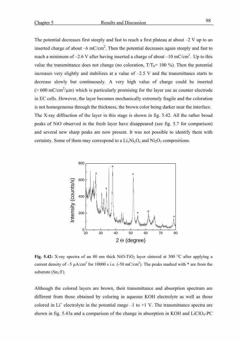
Chapter 5 Results and Discussion
98
The potential decreases first steeply and fast to reach a first plateau at about –2 V up to an
inserted charge of about –6 mC/cm2. Then the potential decreases again steeply and fast to
reach a minimum of –2.6 V after having inserted a charge of about –10 mC/cm2. Up to this
value the transmittance does not change (no coloration, T/Tb= 100 %). Then the potential
increases very slightly and stabilizes at a value of –2.5 V and the transmittance starts to
decrease slowly but continuously. A very high value of charge could be inserted
(> 600 mC/cm2/µm) which is particularly promising for the layer use as counter electrode
in EC cells. However, the layer becomes mechanically extremely fragile and the coloration
is not homogeneous through the thickness, the brown color being darker near the interface.
The X-ray diffraction of the layer in this stage is shown in fig. 5.42. All the rather broad
peaks of NiO observed in the fresh layer have disappeared (see fig. 5.7 for comparison)
and several new sharp peaks are now present. It was not possible to identify them with
certainty. Some of them may correspond to a LixNiyOz and Ni2O3 compositions.
20 30 40 50 60 70 800
200
400
600
800
***
*
*
*
*
Inte
nsity
(cou
nts/
s)
2 Θ (degree)
Fig. 5.42: X-ray spectra of an 80 nm thick NiO-TiO2 layer sintered at 300 °C after applying a
current density of –5 µA/cm2 for 10000 s i.e. (-50 mC/cm2). The peaks marked with * are from the
substrate (Sn2:F).
Although the colored layers are brown, their transmittance and absorption spectrum are
different from those obtained by coloring in aqueous KOH electrolyte as well as those
colored in Li+ electrolyte in the potential range –1 to +1 V. The transmittance spectra are
shown in fig. 5.43a and a comparison of the change in absorption in KOH and LiClO4-PC
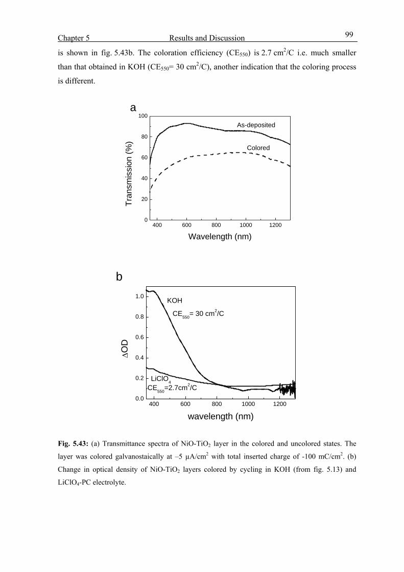
Chapter 5 Results and Discussion
99
is shown in fig. 5.43b. The coloration efficiency (CE550) is 2.7 cm2/C i.e. much smaller
than that obtained in KOH (CE550= 30 cm2/C), another indication that the coloring process
is different.
400 600 800 1000 12000
20
40
60
80
100a
As-deposited
Colored
Tran
smis
sion
(%)
Wavelength (nm)
400 600 800 1000 12000.0
0.2
0.4
0.6
0.8
1.0
b
CE550=2.7cm2/C
CE550= 30 cm2/C
LiClO4
KOH
ΔOD
wavelength (nm)
Fig. 5.43: (a) Transmittance spectra of NiO-TiO2 layer in the colored and uncolored states. The
layer was colored galvanostaically at –5 µA/cm2 with total inserted charge of -100 mC/cm2. (b)
Change in optical density of NiO-TiO2 layers colored by cycling in KOH (from fig. 5.13) and
LiClO4-PC electrolyte.

Chapter 5 Results and Discussion
100
By reversing the current, i.e. by applying +5 µA/cm2 and limiting the potential to 0 V, the
behavior of the potential and the transmittance have been found to depend on the amount
of charge that has been previously incorporated (fig. 5.44).
After having inserted –9 mC/cm2 only (initial period) the voltage jumps quickly to
+0.25 V and the value of the transmittance T/Tb= 100 % is not altered. Then the voltage
increases slightly but steadily to +0.6 V. The layer slightly colors in a way similar to that
observed in fig. 5.38.
When a higher amount of charge has been incorporated (-50 mC/cm2) the potential
increases slowly from –2.4 V and the previously colored layer starts to bleach slowly but
only partly. These results indicate that the EC processes are totally different from those
discussed using aqueous KOH based electrolyte.
0 2 4 6 8 10 12 14 16 180
70
80
90
100
-2.4-1.8-1.2-0.60.00.61.2
-9 mC/cm2
-50 mC/cm2
T/
T blea
ched
(%)
Q (mC/cm2)
-50 mC/cm2
-9 mC/cm2
Vol
tage
vs
. Ag/
AgC
lO4 (
V)
Fig. 5.44: Potential and transmittance changes vs. the de-inserted charge during galvanostatic
measurement at +5µA/cm2 for two single NiO-TiO2 layers after being polarized at a negative
current of –5 µA/cm2 up to an inserted charge of –9 mC/cm2 and -50 mC/cm2.
The sol gel layers follow essentially the same behavior observed by the group of Scrosati
et al. [192, 193, 195] with sputtered layers except that, in their case, the fresh layer was
initially colored and it bleached during the initial period i.e. till the potential reached the
minimum value i.e. after a charge injection of –212 mC/cm2/µm (in our case
-125 mC/cm2/µm).
Our findings are also confirmed by performing CV cycles in the same potential range 0 to
–3 V vs. Ag/AgClO4-PC using fresh uncolored layers. The results shown in fig. 5.45 has
been obtained using a very slow rate of 1 mV/s in order to meet the slow kinetics of the
galvanostatic measurement in fig. 5.41.
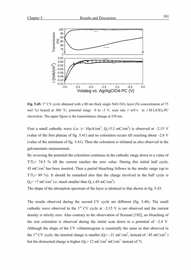
Chapter 5 Results and Discussion
101
-3.0 -2.5 -2.0 -1.5 -1.0 -0.5 0.0-0.12-0.10-0.08-0.06-0.04-0.020.000.02
0
7580859095
100
Volateg vs. Ag/AgClO4-PC (V)
i (m
A/cm
2 )
Tran
smis
sion
(%)
Fig. 5.45: 1st CV cycle obtained with a 80 nm thick single NiO-TiO2 layer (Ni concentration of 75
mol %) heated at 300 °C, potential range 0 to -3 V, scan rate 1 mV/s in 1 M LiClO4-PC
electrolyte. The upper figure is the transmittance change at 550 nm.
First a small cathodic wave (i.e. i< 10µA/cm2, Qc≈5.3 mC/cm2) is observed at –2.15 V
(value of the first plateau of fig. 5.41) and no coloration occurs till reaching about –2.6 V
(value of the minimum of fig. 5.41). Then the coloration is initiated as also observed in the
galvanostatic measurement.
By reversing the potential the coloration continues in the cathodic range down to a value of
T/Tb= 74.5 % till the current reaches the zero value. During this initial half cycle,
45 mC/cm2 has been inserted. Then a partial bleaching follows in the anodic range (up to
T/Tb= 89 %). It should be remarked also that the charge involved in the half cycle is
Qa= +7 mC/cm2 i.e. much smaller than Qc (-45 mC/cm2).
The shape of the absorption spectrum of the layer is identical to that shown in fig. 5.43.
The results observed during the second CV cycle are different (fig. 5.46). The small
cathodic wave observed in the 1st CV cycle at –2.15 V is not observed and the current
density is strictly zero. Also contrary to the observation of Scrosati [192], no bleaching of
the rest coloration is observed during the initial scan down to a potential of –2.4 V.
Although the shape of the CV voltammogram is essentially the same as that observed in
the 1st CV cycle, the inserted charge is smaller (Qc= -21 mC/cm2, instead of –45 mC/cm2 )
but the deinserted charge is higher (Qa= 12 mC/cm2 mC/cm2 instead of 7).

Chapter 5 Results and Discussion
102
-3.0 -2.5 -2.0 -1.5 -1.0 -0.5 0.0
-0.04
-0.02
0.00
07580859095
100
Tran
smis
sion
(
%)
i (m
A/cm
2 )
Voltage vs. Ag/AgClO4-PC (V)
Fig. 5.46: 2nd CV cycle obtained with a 80 nm thick single NiO-TiO2 layer (Ni concentration of
75 mol %) heated at 300 °C, potential range 0 to -3 V, scan rate 1 mV/s in 1 M LiClO4-PC
electrolyte. The upper figure is the transmittance change at 550 nm.
The final coloration of the layer during the cathodic range is not improved (76.5 %) and it
bleaches to a slightly lower value than that obtained after the 1st cycle (T/Tb= 87.5 %). As
the charge involved in the bleaching process is smaller than that involved in the coloring
process, the CV behavior is therefore not fully reversible.
A further interesting observation confirming the above results is shown in fig. 5.47. A
fresh layer has been first submitted to a cyclic voltammetry in the potential range 0 to
-2.15 V, then a galvanostatic measurement has been made using –5µA/cm2.
0 -10 -20 -30 -40 -50-3.0
-2.5
-2.0
-1.5
-1.0
-0.5
0.0
0
65
70
75
80
85
90
95
100
T/T bl
each
ed (%
)
Vola
tge
vs A
g/Ag
ClO
4-PC
(V)
Q (mC/cm2)
Fig. 5.47: Potential and transmittance (550 nm) evolution for 80 nm thick single NiO-TiO2 layer
(Ni content of 75 mol %) in LiClO4-PC during a galvanostatic measurement applying a negative
current density of –5µA/cm2. The layer was previously cycled in the potential range 0 to –2.15 V
for 2 CVs.
Chapter 5 Results and Discussion
103
Contrary to the result shown in fig. 5.41, the potential drops instantly down to –2.75 V and
remains then at a constant value of –2.5 V. This is accompanied by a continuous coloration
of the layer reaching the same value of the transmittance, T/Tb= 68 %, after intercalating
-50 mC/cm2. The initial activation period is therefore not observed so that one can
conclude that this period is linked to the small cathodic wave observed only in the 1st CV
cycle around –2.15 V.
The group of Scrosati has explained the behavior of sputtered NiOx layer cycled in the
same Li+ electrolyte and in the same potential range according to polaron models assuming
that their electrodes consist of amorphous, nonstoichiometric nickel oxide (NiOx), the
deviation from the stoichiometry being ascribable to nickel vacancies. In the as deposited
state, the sputtered electrodes are initially colored due to the presence of Ni3+ necessary to
balance the Ni vacancies. The electrochromic process was therefore divided into two steps.
During the initial period of a galvanostatic process i.e. during the period in which the
potential decreases to a minimum value (see e.g. fig. 5.41), Li+ and e- are injected
irreversibly into the layer according to
NiOx +yLi+ + ye- → LiyNiOx (5.15)
While the Li+ influences the electrochemical behavior of the NiOx electrode, the injection
of electrons influences the electrochromic behavior where they interact with the Ni3+ ions
according to
Ni3+ +e- ↔ Ni2+ (5.16)
colored bleached
This process leads to the progressive elimination of the vacancies and thus to the
elimination of the associated Ni3+ polaron producing transparent LiyNiOx electrode. It
describes in fact a type of activation of the NiOx thin film i.e. an irreversible uptake of Li+
ions in the NiOx host structure inducing phase modification of the original NiOx sample.
This activation step is followed by a further forced reversible injection of Li+ to which an
electrochromic effect is associated according to
LiyNiOx + zLi+ + ze-↔ Liy+zNiOx (5.17)
A convincing evidence for these assumptions was obtained by following the expansion of
the host oxide matrix during this activation process.
When the intercalated charge exceeds a limit (i.e. the value needed for the activation), the
injected electrons may be localized (by interacting with Li+ ions or Ni2+) or delocalized
giving again rise to the formation of polarons. In the later case the mechanism becomes
Chapter 5 Results and Discussion
104
similar to that of a cathodic electrochromic material and the layer colors at a negative
potential.
Our findings however are slightly different because an as deposited sol-gel NiO-TiO2 layer
is initially transparent so that no colored Ni3+ polarons exist. When the layer is polarized at
a negative current, no change in transmittance is observed during the initial period of the
CV cycle until the layer potential reaches –2.6 V vs Ag/AgClO4-PC (see fig. 5.41, 5.45 and
5.46). This value should nevertheless correspond to the Li+ insertion potential. The layer
becomes colored and as observed by the XRD the composition of the electrode changes.
As it was not possible to identify the phases one just label them as LizNiO-TiO2. This
process is not fully reversible neither by reversing the current nor by closing the CV cycle
and part of the injected Li+ ions stay in the electrode so that the layer remains slightly
colored. Our proposal therefore is to divide the reactions of NiO-TiO2 layer in LiClO4-PC
in the potential range 0 to –3 V into three main processes:
i- when applying a negative current galvanostatically (first region) down to a potential of
-2.15 V (-9 mC/cm2) or during the first cathodic CV scan between 0 and –2.15 V.
Here as the electrochemical reaction occurs only once and is irreversible and no coloration
or bleaching of the layer is observed, the proposal of Passerini et al. [192, 193, 195] cannot
be applied. It is proposed instead that the EC process occurring in this potential range is
linked to an irreversible composition change involving either two uncolored compounds as
e.g. NiO and small amounts of Ni(OH)2, or more simply water that are expected to exist in
the layer due to the low sintering temperature (300 °C) and the processing in normal air
(RH= 40 %),.
The first process may involve the following reaction
2Ni(OH)2 + 2e- → 2NiO + 2OH- +H2 (gas) (5.18)
uncolored uncolored
The second process, as it is known from literature, will involve the decomposition of H2O
according to
2H2O + 2e- → 2OH- + H2 (gas) (5.19)
This reaction occurs at –0.827 V vs. NHE i.e. within the voltage range –1.7 to –2.2 V vs.
Ag/AgClO4-PC.
This explains why no coloration of the layer is observed, why only a current is flowing,
and since all OH- groups contained in the layer will react (corresponding to 5.3 mC/cm2)
why the process is irreversible and occurs only once.
Chapter 5 Results and Discussion
105
ii- when applying a negative current galvanostatically during the constant potential of
-2..6 V (long plateau of fig. 5.41) or during the cathodic range of CV cycle down to –3 V.
The proposal of Scrosati is quite possible. Li+ together with e- may effectively be
incorporated cathodically into the layer according to
NiO-TiO2 + zLi+ +ze- → LizNiO-TiO2 (5.20)
bleached colored
As shown in fig 5.42 the composition of the layer has changed drastically and
unfortunately it was not yet possible to identify the components Therefore one can only
assume that the coloration is due to electrons localized by interacting with Ni2+ or most
likely with defects involving Li+ ions or delocalized giving rise to the formation of
polarons. In any case a mechanism similar to that of cathodic electrochromic material like
WO3, Nb2O5 is observed and the layer becomes colored with an absorption spectrum
different from that observed in KOH electrolyte (due to NiOOH).
The fact that the coloration efficiency during this process is rather small (about 2 mC/cm2)
may indicate that not all inserted Li+ ions lead to the formation of active (colored) centers
and mostly participate to the modification of the phases of the layer contributing to its
fragility, (expansion of the host oxide matrix). If that reaction is reversible is not yet
known.
iii- when reversing the galvanostatic current and limiting the potential to about 0 V or
during an anodic CV scan up to 0 V.
As the layer does not bleach completely it is probable that Li+ ions are deinserted slowly
out of the layer according to
LizNiO-TiO2 → Liz-yNiO-TiO2 + y Li+ +y e- (5.21)
colored less colored
Therefore by further cycling the composition of the layer will oscillate between
LiaNiO-TiO2 and LibNiO-TiO2 according to
LiaNiO-TiO2 ↔ LibNiO-TiO2 (5.22)
higher T (%) lower T (%)
where b> a.

Chapter 5 Results and Discussion
106
c) Potential range +1V to –3V vs. Ag/AgClO4-PC
It was shown in section a) and b) that the sol-gel NiO-TiO2 layers can be colored either
cathodically (potential range < 0V) or anodically (potential range > 0V) in LiClO4-PC
electrolyte. This is an interesting for the development of EC devices. It is however
necessary to find out if the mechanisms outlined above interfere or not. A Fresh 80 nm
thick layer sintered at 300 °C have been therefore switched in the whole potential range –3
to +1 V vs. Ag/AgClO4-PC
Fig. 5.48 shows three galvanostatic measurements made in sequence with a total charge of
50 mC/cm2 by applying
a) –5 µA/cm2 then
b) +5 µA/cm2again
c) –5 µA/cm2 (as in a)
0 -10 -20 -30 -40 -50
-2.5
-2.0
-1.5
-1.0
-0.5
0.0
0.5
1.0
0
60
65
70
75
80
85
90
95
100
T/T bl
each
ed (%
)
Vo
ltage
vs.
Ag/
AgC
lO4-P
C (V
)
Q (mC/cm2)
a
0 10 20 30 40 500
65
70
75
80
85
90
95
100
-2.5
-2.0
-1.5
-1.0
-0.5
0.0
0.5
1.0
T/T bl
each
ed (%
)
b
Vo
ltage
vs.
Ag/
AgC
lO4-P
C(V
)
Q (mC/cm2)
-2.5
-2.0
-1.5
-1.0
-0.5
0.0
0.5
1.0
0 -10 -20 -30 -40 -500
60
65
70
75
80
85
90
95
100
Vol
tage
vs.
Ag/
AgC
lO4-
PC (V
)
c
T/T bl
each
ed (%
)
Q (mC/cm2)
Fig. 5.48: Potential and transmittance (550 nm) evolution for 80 nm thick single NiO-TiO2 layer
(Ni content of 75 mol %) in LiClO4-PC during a galvanostatic measurement applying (a) a negative
current density of –5µA/cm2, then (b) positive current of + 5µA/cm2, then (c) again negative
current of –5µA/cm2
Chapter 5 Results and Discussion
107
Fig. 5.48a is similar to that shown in fig. 5.41 and the results have been discussed already
in section b). The coloration obtained after incorporating –50 mC/cm2 was assumed to be
due to simultaneous insertion of Li+ and e- and the composition of the layer was drastically
altered.
The initial part of fig. 5.48b is also similar to fig. 5.44. However it is observed that the
potential drastically increases after a charge insertion of about +15 mC/cm2 to level up
around + 1V. The transmittance starts also to increase later, passing by a maximum at
potential of +0.5 V and then continuously decreases down to about T/Tb= 65 %.
In section a) it was shown that fresh NiO-TiO2 layers could be slightly colored
(∆T/Tb=9- 13 %) in this potential range (V> 0V vs. Ag/AgClO4-PC) and this was
explained by the incorporation of traces of OH-. After a first Li+ ion insertion however, the
composition of the layer have been drastically altered so that the above mechanism is
certainly not valid.
Therefore, without performing more detailed and certainly high complex investigations, it
is not possible at the present time to propose a mechanism for this coloration.
Fig. 48c shows the results obtained by applying again a negative small current density of
- 5 µA/cm2. Since the layer is colored (see fig. 5.48b) the behavior recorded is different
from that shown during the first galvanostatic test (fig. 5.48a). The potential drop to the
last plateau at –2.5V occurs now in two steps and is accompanied by a very fast increase of
the transmittance from ∆T/Tb= 65 % up to 100 % (the complete bleaching of the layer)
after using a charge of 5 mC/cm2 only then as before the layer remains uncolored till the
end of the first plateau and as before starts to color during the second plateau with exactly
the same kinetics. The initial behavior is now identical to that found by Scrosati group
[194] with fresh colored sputtered NiO layers. As the bleaching of the layer is fast and
needs only about 5 mC/cm2, the process may only involve electrons that recombine with
the colored species. However such phenomenon is not observed with the defects that give
rise to the coloration due to the insertion of Li+ and e- (fig. 5.46a), but only with those
colored during the very slow coloration obtained after that deinsertion (fig. 5.48b).

Chapter 5 Results and Discussion
108
5.6 Characterization of CeO2-TiO2 layer in KOH A CeO2-TiO2 layer is used in this work as counter electrode together with a NiO-TiO2 layer
as working electrode to build electrochromic devices. So it is important to test it in KOH
electrolyte.
Cyclic voltammetric recordings were performed in order to obtain electrochemical
fingerprints of the studied CeO2-TiO2 layers in aqueous basic solution of 1 M KOH
(fig. 5.49a). The potential in each measurement was swept from –1.2 to +0.7 V vs. SCE. A
well defined anodic peak occurs at –0.238 V while the cathodic peak occurs at –0.63 V.
The stability of the layers was checked by cycling up to 2000 cycles. A stable response
was achieved after 50 cycles where no change in peak current density was noticed. The
cathodic and anodic charges are almost the same indicating that the insertion process is
highly reversible and no faradic process occurs in parallel to the electrochromic charging
process (fig. 5.49b).
-1.0 -0.5 0.0 0.5
-0.2
-0.1
0.0
0.1
0.2
a
CV no. 10 100 500 1000
i(mA/
cm2 )
Voltage vs. SCE (V)0 200 400 600 800 1000
0
2
4
6
8
10
12
14
16
b
Qa
Qc
Q (m
C/c
m2 )
Cycle number
Fig. 5.49: Typical CV voltamogramms up to 1000 cycles for a 200 nm thick single CeO2-TiO2
layer heated at 550 °C, potential range -1.2 to 0.7V, scan rate 10 mV/s in 1 M KOH. (b) Calculated
charge density in the anodic (Qa) and cathodic (Qc) range.
a) Layer thickness
The dependence of the CV response on the film thickness is depicted in fig. 5.50. The
current density increases by increasing the thickness up to 240 nm. Increasing the layer
thickness also shifts the anodic peak slightly to more positive potential values while the
cathodic peak shifts to more negative potentials.
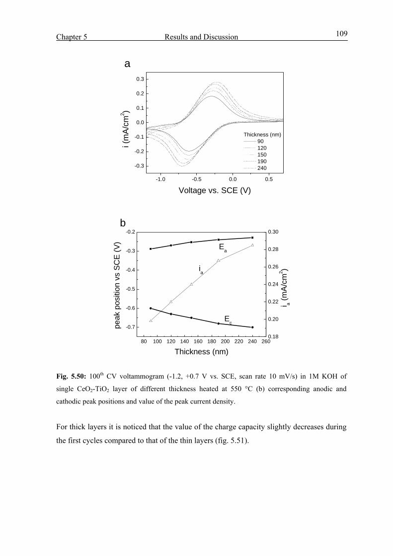
Chapter 5 Results and Discussion
109
-1.0 -0.5 0.0 0.5
-0.3
-0.2
-0.1
0.0
0.1
0.2
0.3
a
Thickness (nm) 90 120 150 190 240
i (m
A/cm
2 )
Voltage vs. SCE (V)
80 100 120 140 160 180 200 220 240 260
-0.7
-0.6
-0.5
-0.4
-0.3
-0.2
0.18
0.20
0.22
0.24
0.26
0.28
0.30
ia
b
Ea
Ec
peak
pos
ition
vs
SCE
(V)
Thickness (nm)
i a (m
A/cm
2 )
Fig. 5.50: 100th CV voltammogram (-1.2, +0.7 V vs. SCE, scan rate 10 mV/s) in 1M KOH of
single CeO2-TiO2 layer of different thickness heated at 550 °C (b) corresponding anodic and
cathodic peak positions and value of the peak current density.
For thick layers it is noticed that the value of the charge capacity slightly decreases during
the first cycles compared to that of the thin layers (fig. 5.51).

Chapter 5 Results and Discussion
110
0 20 40 60 80 1000
5
10
15
20
240 nm
190 nm
150 nm
120 nm
90 nm
Qa(m
C/c
m2 )
Cycle number
Fig. 5.51: Anodic charge density during 100 CV cycles (-1.2, +0.7 V, scan rate 10 mV/s) in 1 M
KOH of single CeO2-TiO2 layers of different thickness heated at 550 °C.
b) Scan rate
CV voltammograms at different scan rates in the range between 1 to 7 mV/s and 10 to
500 mV/s are shown in fig. 5.52a and b respectively for single layer 200 nm thick. In both
cases the value of the anodic and cathodic current density raises and at high scan rates the
cathodic peaks are not completed.
-1.5 -1.2 -0.9 -0.6 -0.3 0.0 0.3 0.6 0.9-0.20
-0.15
-0.10
-0.05
0.00
0.05
0.10
0.15
0.20a
scan rate 0.5 1.5 3.5 5 7
i (m
A/cm
2 )
Voltage vs. SCE (V)-1.0 -0.5 0.0 0.5
-1.5
-1.0
-0.5
0.0
0.5
1.0
b
Scan rate 10 20 50 100 200 300 400 500
i (m
A/cm
2 )
Voltage vs. SCE (mV)
Fig. 5.52: CV voltammograms (-1.2, +0.7 V) of a 200 nm thick single CeO2-TiO2 tested in 1 M
KOH at different scan rates (a) up to 10 mV/s (b) higher than 10 mV/s
In general, for a redox reaction to be reversible, the concentrations of the oxidized and
reduced species at the electrode surface must be maintained at the values defined by the
Nernst equation. In practical terms, a redox reaction is reversible if the rate of electrons
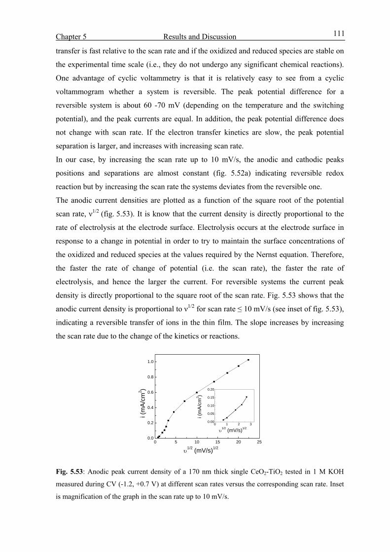
Chapter 5 Results and Discussion
111
transfer is fast relative to the scan rate and if the oxidized and reduced species are stable on
the experimental time scale (i.e., they do not undergo any significant chemical reactions).
One advantage of cyclic voltammetry is that it is relatively easy to see from a cyclic
voltammogram whether a system is reversible. The peak potential difference for a
reversible system is about 60 -70 mV (depending on the temperature and the switching
potential), and the peak currents are equal. In addition, the peak potential difference does
not change with scan rate. If the electron transfer kinetics are slow, the peak potential
separation is larger, and increases with increasing scan rate.
In our case, by increasing the scan rate up to 10 mV/s, the anodic and cathodic peaks
positions and separations are almost constant (fig. 5.52a) indicating reversible redox
reaction but by increasing the scan rate the systems deviates from the reversible one.
The anodic current densities are plotted as a function of the square root of the potential
scan rate, ν1/2 (fig. 5.53). It is know that the current density is directly proportional to the
rate of electrolysis at the electrode surface. Electrolysis occurs at the electrode surface in
response to a change in potential in order to try to maintain the surface concentrations of
the oxidized and reduced species at the values required by the Nernst equation. Therefore,
the faster the rate of change of potential (i.e. the scan rate), the faster the rate of
electrolysis, and hence the larger the current. For reversible systems the current peak
density is directly proportional to the square root of the scan rate. Fig. 5.53 shows that the
anodic current density is proportional to ν1/2 for scan rate ≤ 10 mV/s (see inset of fig. 5.53),
indicating a reversible transfer of ions in the thin film. The slope increases by increasing
the scan rate due to the change of the kinetics or reactions.
0 5 10 15 20 250.0
0.2
0.4
0.6
0.8
1.0
0 1 2 30.00
0.05
0.10
0.15
0.20
υ1/2 (mV/s)1/2
i (m
A/cm
2 )
i (m
A/cm
2 )
υ1/2 (mV/s)1/2
Fig. 5.53: Anodic peak current density of a 170 nm thick single CeO2-TiO2 tested in 1 M KOH
measured during CV (-1.2, +0.7 V) at different scan rates versus the corresponding scan rate. Inset
is magnification of the graph in the scan rate up to 10 mV/s.
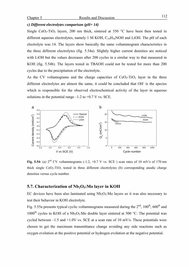
Chapter 5 Results and Discussion
112
c) Different electrolytes comparison (pH= 14)
Single CeO2-TiO2 layers, 200 nm thick, sintered at 550 °C have been then tested in
different aqueous electrolytes, namely 1 M KOH, C16H36NOH and LiOH. The pH of each
electrolyte was 14. The layers show basically the same voltammogram characteristics in
the three different electrolytes (fig. 5.54a). Slightly higher current densities are noticed
with LiOH but the values decreases after 200 cycles in a similar way to that measured in
KOH (fig. 5.54b). The layers tested in TBAOH could not be tested for more than 200
cycles due to the precipitation of the electrolyte.
As the CV voltamograms and the charge capacities of CeO2-TiO2 layer in the three
different electrolytes are almost the same, it could be concluded that OH- is the species
which is responsible for the observed electrochemical activity of the layer in aqueous
solutions in the potential range –1.2 to +0.7 V vs. SCE.
-1.5 -1.0 -0.5 0.0 0.5 1.0-0.5
-0.4
-0.3
-0.2
-0.1
0.0
0.1
0.2
0.3
0.4a
TBAOH KOH LiOH
Cur
rent
den
sity
(mA/
cm2 )
V vs SCE (V)
0 200 400 600 800 10000
5
10
15
20
b
TBAOH
KOH
LiOH
Qa (
mC
/cm
2 )
Cycle number
Fig. 5.54: (a) 2nd CV voltammograms (-1.2, +0.7 V vs. SCE ) scan rates of 10 mV/s of 170 nm
thick single CeO2-TiO2 tested in three different electrolytes (b) corresponding anodic charge
densities versus cycle number.
5.7. Characterization of Nb2O5:Mo layer in KOH EC devices have been also laminated using Nb2O5:Mo layers so it was also necessary to
test their behavior in KOH electrolyte.
Fig. 5.55a presents typical cyclic voltammograms measured during the 2nd, 100th, 600th and
1000th cycles in KOH of a Nb2O5:Mo double layer sintered at 500 °C. The potential was
cycled between –1.5 and +1.0V vs. SCE at a scan rate of 10 mV/s. These potentials were
chosen to get the maximum transmittance change avoiding any side reactions such as
oxygen evolution at the positive potential or hydrogen evolution at the negative potential.

Chapter 5 Results and Discussion
113
-1.5 -1.0 -0.5 0.0 0.5 1.0-0.4
-0.3
-0.2
-0.1
0.0
0.1
55
60
65
70
75
80a
1000th CV600thCV
1stCV
i (m
A/cm
2 )
Voltage vs. SCE (V)
Tran
smis
sion
(%)
0 200 400 600 800 10000
2
4
6
8
10
12
14
16
0.00
0.05
0.10
0.15
0.20
0.25
0.30
Qc (
mC
/cm
2 )
Cycle number
b
ΔO
D (5
50 n
m)
ΔOD
Qc
Fig. 5.55: Typical CV voltammograms up to 1000 cycles of a 160 nm thick double Nb2O5:Mo
layer heated at 500 °C, potential range -1.5 to 1.0 V, scan rate 10 mV/s in 1 M KOH. The dotted
line is the transmittance (T) measured during the 100th cycle at λ= 550 nm. (b) Corresponding
charge capacity Qc and change in optical density ΔOD.
A broad cathodic peak associated with the layer coloration is seen around –1.2 V. In the
initial cycling, only one side of the peak is reached and it interferes with the hydrogen
evolution peak at the end of the cathodic scan. By cycling, the peak becomes better defined
and separated from the hydrogen evolution peak. A broad anodic peak accompanied by the
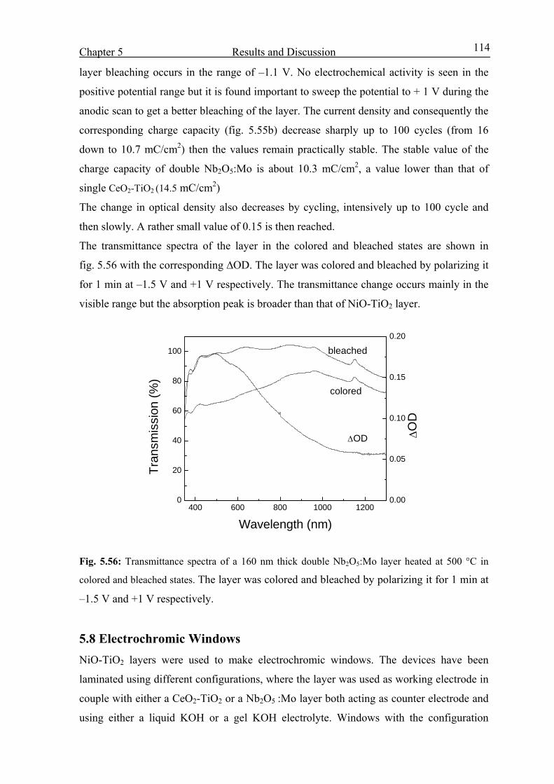
Chapter 5 Results and Discussion
114
layer bleaching occurs in the range of –1.1 V. No electrochemical activity is seen in the
positive potential range but it is found important to sweep the potential to + 1 V during the
anodic scan to get a better bleaching of the layer. The current density and consequently the
corresponding charge capacity (fig. 5.55b) decrease sharply up to 100 cycles (from 16
down to 10.7 mC/cm2) then the values remain practically stable. The stable value of the
charge capacity of double Nb2O5:Mo is about 10.3 mC/cm2, a value lower than that of
single CeO2-TiO2 (14.5 mC/cm2)
The change in optical density also decreases by cycling, intensively up to 100 cycle and
then slowly. A rather small value of 0.15 is then reached.
The transmittance spectra of the layer in the colored and bleached states are shown in
fig. 5.56 with the corresponding ∆OD. The layer was colored and bleached by polarizing it
for 1 min at –1.5 V and +1 V respectively. The transmittance change occurs mainly in the
visible range but the absorption peak is broader than that of NiO-TiO2 layer.
400 600 800 1000 12000
20
40
60
80
100
0.00
0.05
0.10
0.15
0.20
colored
bleached
Tran
smis
sion
(%)
Wavelength (nm)
ΔOD
ΔOD
Fig. 5.56: Transmittance spectra of a 160 nm thick double Nb2O5:Mo layer heated at 500 °C in
colored and bleached states. The layer was colored and bleached by polarizing it for 1 min at
–1.5 V and +1 V respectively.
5.8 Electrochromic Windows NiO-TiO2 layers were used to make electrochromic windows. The devices have been
laminated using different configurations, where the layer was used as working electrode in
couple with either a CeO2-TiO2 or a Nb2O5 :Mo layer both acting as counter electrode and
using either a liquid KOH or a gel KOH electrolyte. Windows with the configuration
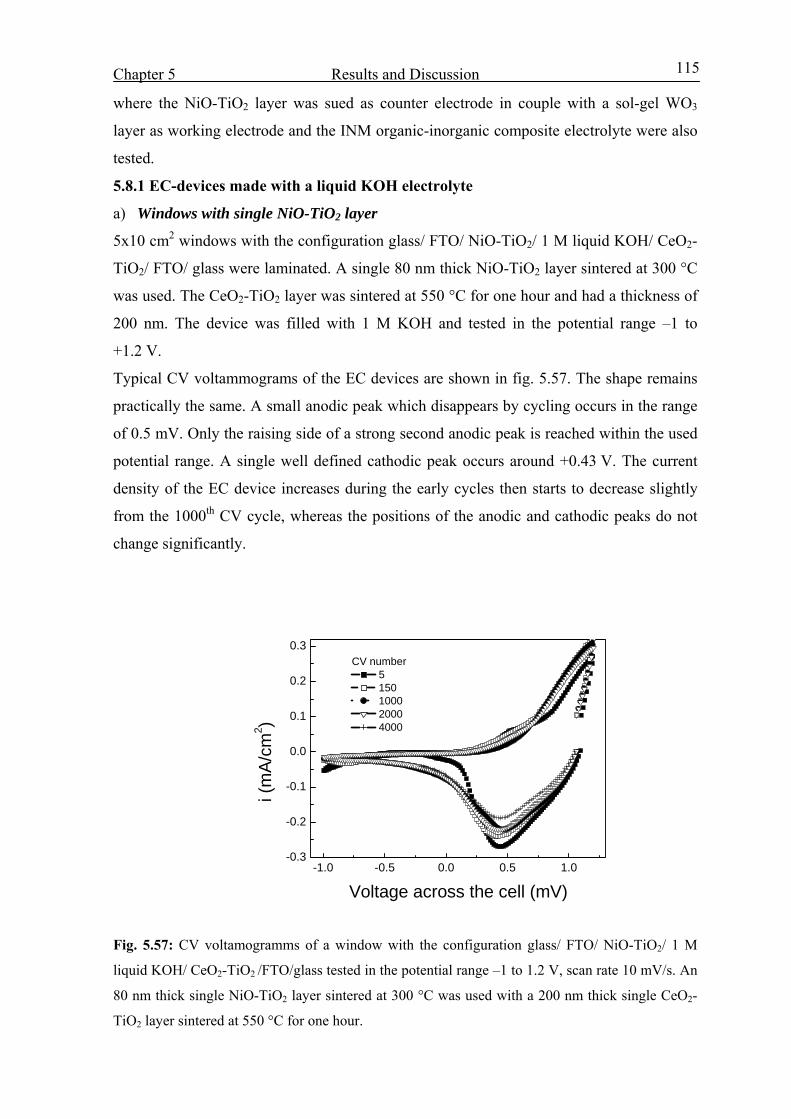
Chapter 5 Results and Discussion
115
where the NiO-TiO2 layer was sued as counter electrode in couple with a sol-gel WO3
layer as working electrode and the INM organic-inorganic composite electrolyte were also
tested.
5.8.1 EC-devices made with a liquid KOH electrolyte
a) Windows with single NiO-TiO2 layer
5x10 cm2 windows with the configuration glass/ FTO/ NiO-TiO2/ 1 M liquid KOH/ CeO2-
TiO2/ FTO/ glass were laminated. A single 80 nm thick NiO-TiO2 layer sintered at 300 °C
was used. The CeO2-TiO2 layer was sintered at 550 °C for one hour and had a thickness of
200 nm. The device was filled with 1 M KOH and tested in the potential range –1 to
+1.2 V.
Typical CV voltammograms of the EC devices are shown in fig. 5.57. The shape remains
practically the same. A small anodic peak which disappears by cycling occurs in the range
of 0.5 mV. Only the raising side of a strong second anodic peak is reached within the used
potential range. A single well defined cathodic peak occurs around +0.43 V. The current
density of the EC device increases during the early cycles then starts to decrease slightly
from the 1000th CV cycle, whereas the positions of the anodic and cathodic peaks do not
change significantly.
-1.0 -0.5 0.0 0.5 1.0-0.3
-0.2
-0.1
0.0
0.1
0.2
0.3
CV number 5 150 1000 2000 4000
i (m
A/cm
2 )
Voltage across the cell (mV)
Fig. 5.57: CV voltamogramms of a window with the configuration glass/ FTO/ NiO-TiO2/ 1 M
liquid KOH/ CeO2-TiO2 /FTO/glass tested in the potential range –1 to 1.2 V, scan rate 10 mV/s. An
80 nm thick single NiO-TiO2 layer sintered at 300 °C was used with a 200 nm thick single CeO2-
TiO2 layer sintered at 550 °C for one hour.
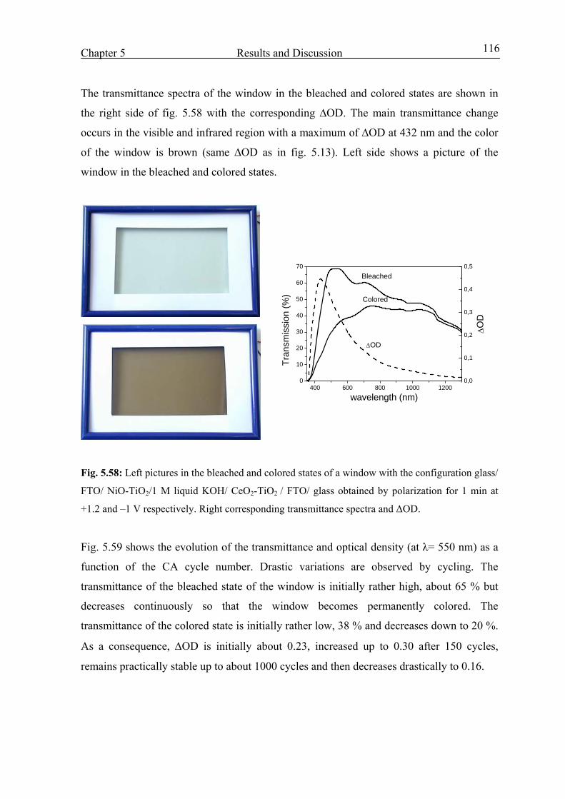
Chapter 5 Results and Discussion
116
The transmittance spectra of the window in the bleached and colored states are shown in
the right side of fig. 5.58 with the corresponding ∆OD. The main transmittance change
occurs in the visible and infrared region with a maximum of ∆OD at 432 nm and the color
of the window is brown (same ∆OD as in fig. 5.13). Left side shows a picture of the
window in the bleached and colored states.
Fig. 5.58: Left pictures in the bleached and colored states of a window with the configuration glass/
FTO/ NiO-TiO2/1 M liquid KOH/ CeO2-TiO2 / FTO/ glass obtained by polarization for 1 min at
+1.2 and –1 V respectively. Right corresponding transmittance spectra and ΔOD.
Fig. 5.59 shows the evolution of the transmittance and optical density (at λ= 550 nm) as a
function of the CA cycle number. Drastic variations are observed by cycling. The
transmittance of the bleached state of the window is initially rather high, about 65 % but
decreases continuously so that the window becomes permanently colored. The
transmittance of the colored state is initially rather low, 38 % and decreases down to 20 %.
As a consequence, ΔOD is initially about 0.23, increased up to 0.30 after 150 cycles,
remains practically stable up to about 1000 cycles and then decreases drastically to 0.16.
400 600 800 1000 12000
10
20
30
40
50
60
70
0,0
0,1
0,2
0,3
0,4
0,5
ΔOD
Bleached
Colored
Tran
smis
sion
(%)
wavelength (nm)
ΔOD
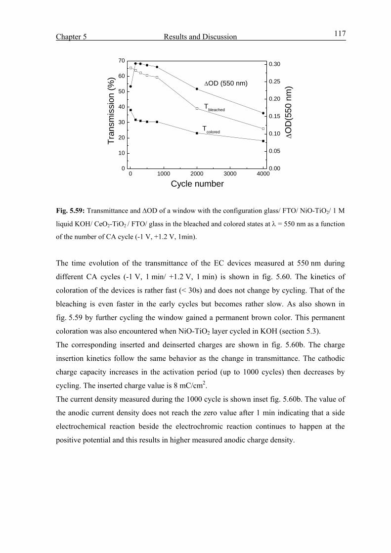
Chapter 5 Results and Discussion
117
0 1000 2000 3000 40000
10
20
30
40
50
60
70
0.00
0.05
0.10
0.15
0.20
0.25
0.30
ΔOD (550 nm)
ΔOD
(550
nm
)
Tbleached
Tcolored
Tran
smis
sion
(%)
Cycle number
Fig. 5.59: Transmittance and ΔOD of a window with the configuration glass/ FTO/ NiO-TiO2/ 1 M
liquid KOH/ CeO2-TiO2 / FTO/ glass in the bleached and colored states at λ = 550 nm as a function
of the number of CA cycle (-1 V, +1.2 V, 1min).
The time evolution of the transmittance of the EC devices measured at 550 nm during
different CA cycles (-1 V, 1 min/ +1.2 V, 1 min) is shown in fig. 5.60. The kinetics of
coloration of the devices is rather fast (< 30s) and does not change by cycling. That of the
bleaching is even faster in the early cycles but becomes rather slow. As also shown in
fig. 5.59 by further cycling the window gained a permanent brown color. This permanent
coloration was also encountered when NiO-TiO2 layer cycled in KOH (section 5.3).
The corresponding inserted and deinserted charges are shown in fig. 5.60b. The charge
insertion kinetics follow the same behavior as the change in transmittance. The cathodic
charge capacity increases in the activation period (up to 1000 cycles) then decreases by
cycling. The inserted charge value is 8 mC/cm2.
The current density measured during the 1000 cycle is shown inset fig. 5.60b. The value of
the anodic current density does not reach the zero value after 1 min indicating that a side
electrochemical reaction beside the electrochromic reaction continues to happen at the
positive potential and this results in higher measured anodic charge density.
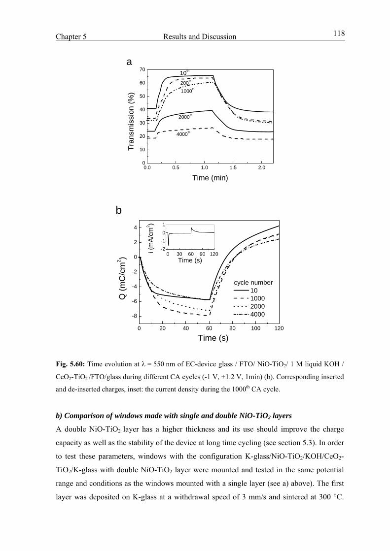
Chapter 5 Results and Discussion
118
0.0 0.5 1.0 1.5 2.00
10
20
30
40
50
60
70a
4000th
2000th
1000th
200th
10th
Tran
smis
sion
(%)
Time (min)
0 20 40 60 80 100 120
-8
-6
-4
-2
0
2
4
0 30 60 90 120-2-101
i (m
A/c
m2 )
Time (s)
b
cycle number 10 1000 2000 4000
Time (s)
Q (m
C/c
m2 )
Fig. 5.60: Time evolution at λ = 550 nm of EC-device glass / FTO/ NiO-TiO2/ 1 M liquid KOH /
CeO2-TiO2 /FTO/glass during different CA cycles (-1 V, +1.2 V, 1min) (b). Corresponding inserted
and de-inserted charges, inset: the current density during the 1000th CA cycle.
b) Comparison of windows made with single and double NiO-TiO2 layers
A double NiO-TiO2 layer has a higher thickness and its use should improve the charge
capacity as well as the stability of the device at long time cycling (see section 5.3). In order
to test these parameters, windows with the configuration K-glass/NiO-TiO2/KOH/CeO2-
TiO2/K-glass with double NiO-TiO2 layer were mounted and tested in the same potential
range and conditions as the windows mounted with a single layer (see a) above). The first
layer was deposited on K-glass at a withdrawal speed of 3 mm/s and sintered at 300 °C.

Chapter 5 Results and Discussion
119
The second layer was deposited on the top of the first one and sintered at the same
temperature. The thickness of the single layer was 80 nm, so that 160 nm is expected for
the double layer.
Fig. 5.61 shows the voltammograms of windows made with single and double NiO-TiO2
layers. They have practically the same shape except a small shift in the anodic and cathodic
peak positions of the window with double NiO-TiO2. No difference is noticed in the
current density of the two windows.
-1.0 -0.5 0.0 0.5 1.0
-0.3
-0.2
-0.1
0.0
0.1
0.2
0.3
i(mA/
cm2 )
Voltage across the window (V)
single layer double layer
Fig. 5.61: CV voltammograms of windows with the configuration K glass/ NiO-TiO2/ KOH/ CeO2-
TiO2/ K-glass with single (⎯) and double (…) NiO-TiO2 layers.
However the use of a double layer improves especially the cycling stability of the
transmittance of the window in the bleached state that decreases only slightly by cycling
from 70 % (initial cycles) down to 60 % after 7000 CA cycles so that the transmittance of
the device in the bleached state remains largely unaltered contrary to the behavior observed
with a single layer (fig.5.62a). However the transmittance of the colored state is somewhat
higher (30 % after 7000 cycles). The change of the optical density at 550 nm is therefore
somewhat different and the device still works very well after 7000 cycles. By further
cycling a corrosion starts to occur at the edge of the devices.
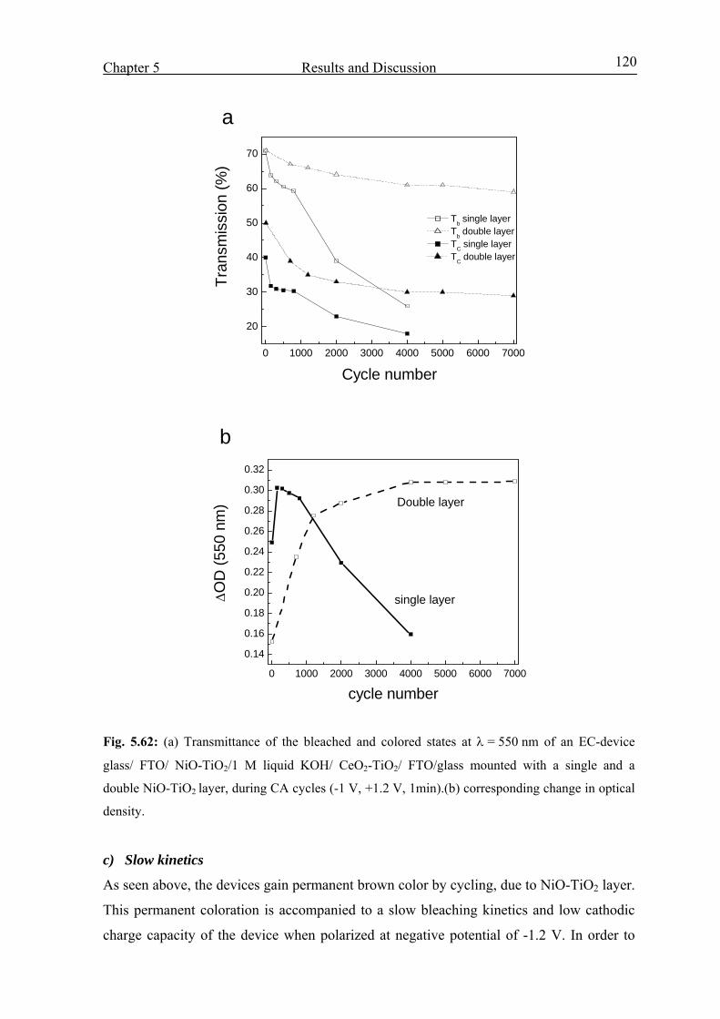
Chapter 5 Results and Discussion
120
0 1000 2000 3000 4000 5000 6000 7000
20
30
40
50
60
70
a
Tran
smis
sion
(%)
Cycle number
Tb single layer T
b double layer
TC single layer TC double layer
0 1000 2000 3000 4000 5000 6000 7000
0.14
0.16
0.18
0.20
0.22
0.24
0.26
0.28
0.30
0.32
b
Double layer
single layer
ΔOD
(550
nm
)
cycle number
Fig. 5.62: (a) Transmittance of the bleached and colored states at λ = 550 nm of an EC-device
glass/ FTO/ NiO-TiO2/1 M liquid KOH/ CeO2-TiO2/ FTO/glass mounted with a single and a
double NiO-TiO2 layer, during CA cycles (-1 V, +1.2 V, 1min).(b) corresponding change in optical
density.
c) Slow kinetics
As seen above, the devices gain permanent brown color by cycling, due to NiO-TiO2 layer.
This permanent coloration is accompanied to a slow bleaching kinetics and low cathodic
charge capacity of the device when polarized at negative potential of -1.2 V. In order to
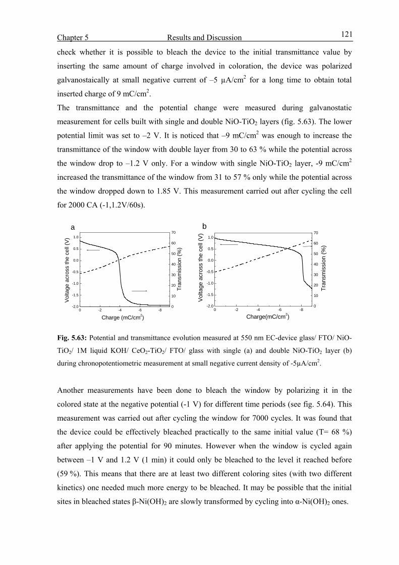
Chapter 5 Results and Discussion
121
check whether it is possible to bleach the device to the initial transmittance value by
inserting the same amount of charge involved in coloration, the device was polarized
galvanostaically at small negative current of –5 µA/cm2 for a long time to obtain total
inserted charge of 9 mC/cm2.
The transmittance and the potential change were measured during galvanostatic
measurement for cells built with single and double NiO-TiO2 layers (fig. 5.63). The lower
potential limit was set to –2 V. It is noticed that –9 mC/cm2 was enough to increase the
transmittance of the window with double layer from 30 to 63 % while the potential across
the window drop to –1.2 V only. For a window with single NiO-TiO2 layer, -9 mC/cm2
increased the transmittance of the window from 31 to 57 % only while the potential across
the window dropped down to 1.85 V. This measurement carried out after cycling the cell
for 2000 CA (-1,1.2V/60s).
-2.0
-1.5
-1.0
-0.5
0.0
0.5
1.0
0 -2 -4 -6 -80
10
20
30
40
50
60
70
a
Volta
ge a
cros
s th
e ce
ll (V
)
Tran
smis
sion
(%)
Charge (mC/cm2)0 -2 -4 -6 -8
-2.0
-1.5
-1.0
-0.5
0.0
0.5
1.0
0
10
20
30
40
50
60
70
Tran
smis
sion
(%)
b
Volta
ge a
cros
s th
e ce
ll (V
)
Charge(mC/cm2)
Fig. 5.63: Potential and transmittance evolution measured at 550 nm EC-device glass/ FTO/ NiO-
TiO2/ 1M liquid KOH/ CeO2-TiO2/ FTO/ glass with single (a) and double NiO-TiO2 layer (b)
during chronopotentiometric measurement at small negative current density of -5µA/cm2.
Another measurements have been done to bleach the window by polarizing it in the
colored state at the negative potential (-1 V) for different time periods (see fig. 5.64). This
measurement was carried out after cycling the window for 7000 cycles. It was found that
the device could be effectively bleached practically to the same initial value (T= 68 %)
after applying the potential for 90 minutes. However when the window is cycled again
between –1 V and 1.2 V (1 min) it could only be bleached to the level it reached before
(59 %). This means that there are at least two different coloring sites (with two different
kinetics) one needed much more energy to be bleached. It may be possible that the initial
sites in bleached states β-Ni(OH)2 are slowly transformed by cycling into α-Ni(OH)2 ones.
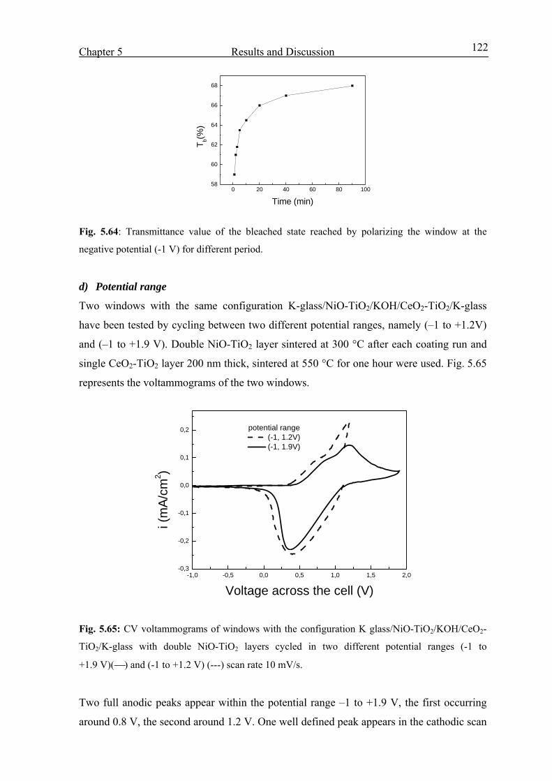
Chapter 5 Results and Discussion
122
0 20 40 60 80 10058
60
62
64
66
68
T b(%)
Time (min)
Fig. 5.64: Transmittance value of the bleached state reached by polarizing the window at the
negative potential (-1 V) for different period.
d) Potential range
Two windows with the same configuration K-glass/NiO-TiO2/KOH/CeO2-TiO2/K-glass
have been tested by cycling between two different potential ranges, namely (–1 to +1.2V)
and (–1 to +1.9 V). Double NiO-TiO2 layer sintered at 300 °C after each coating run and
single CeO2-TiO2 layer 200 nm thick, sintered at 550 °C for one hour were used. Fig. 5.65
represents the voltammograms of the two windows.
-1,0 -0,5 0,0 0,5 1,0 1,5 2,0-0,3
-0,2
-0,1
0,0
0,1
0,2
potential range (-1, 1.2V) (-1, 1.9V)
i (m
A/cm
2 )
Voltage across the cell (V)
Fig. 5.65: CV voltammograms of windows with the configuration K glass/NiO-TiO2/KOH/CeO2-
TiO2/K-glass with double NiO-TiO2 layers cycled in two different potential ranges (-1 to
+1.9 V)(⎯) and (-1 to +1.2 V) (---) scan rate 10 mV/s.
Two full anodic peaks appear within the potential range –1 to +1.9 V, the first occurring
around 0.8 V, the second around 1.2 V. One well defined peak appears in the cathodic scan

Chapter 5 Results and Discussion
123
in the range of 0.3 V. The voltammogram of the window cycled between –1 and 1.2 V has
the same feature but the second anodic peak is not complete and only the raising edge of
the peak is reached. Beside the electrochromic reaction another reaction is expected to
occur at the positive potential. The current density does not go to zero in the falling edge of
the second anodic peak, but, on the contrary, it starts to increase again probably because of
the oxygen evolution.
Although the second anodic peak is complete for –1 to +1.9 V scan range, the
transmittance change, ∆OD and the long time stability of the devices are comparatively
worse (see fig. 5.66). This confirms that the use of a higher positive potential leads to a
faster degradation of NiO-TiO2 layer as discussed before in section 5.3b.
Therefore increasing the positive voltage range to get the full second anodic peak did not
improve the coloration contrast of the window and on the other hand caused a faster
degradation of the device.
0 1000 2000 3000 4000 5000 6000 70000
10
20
30
40
50
60
70
a
(-1, 1.2V)bleached (-1, 1.2V)coloured (-1, 1.9V)bleached (-1, 1.9V)coloured
Tran
smis
sion
(%)
Cycle number0 1000 2000 3000 4000 5000 6000 7000
0,00
0,04
0,08
0,12
0,16
0,20
0,24
0,28
0,32
b
(-1 V, 1.2 V) (-1 V, 1.9 V)
ΔOD
Cycle numbers
Fig. 5.66: (a) Transmittance of the bleached and colored states measured at 550 nm of EC-device
glass/FTO/NiO-TiO2/1 M liquid KOH/CeO2-TiO2 /FTO/glass with double NiO-TiO2 layer, during
CA cycles in two different potential ranges. (b) corresponding change of the optical density.
A macroscopic pictures of EC devices with double NiO-TiO2 layer before and after
degradation are shown in fig. 5.67.

Chapter 5 Results and Discussion
124
Fig. 5.67: Macroscopic pictures of EC devices with the configuration device glass/ FTO/ NiO-
TiO2/1 M liquid KOH/CeO2-TiO2 / FTO/ glass with double NiO-TiO2 layer before (left) and after
degradation (right).
5.8.2 EC-devices built with NiO-TiO2 layers protected against corrosion
The long time stability of the devices based on NiO-TiO2 layers is not high (almost 7000
cycles) as layers degrade when cycled in KOH electrolyte. It is known from the literature
that thin layers of dielectric oxides may be used as anticorrosion layers. Following these
ideas thin layers of ZrO2, TiO2, Al2O3 and CeO2-TiO2 (all 20 to 25 nm thick) have been
deposited on top of the NiO-TiO2 layer to improve the corrosion resistance in KOH
electrolyte and therefore the cycling stability. After depositing single NiO-TiO2 layer and
sintering at 300 °C, a thin protective layer was deposited by dip coating at a very small
drawing speed (0.5 mm/s) and then sintered at 300 °C. It was not possible to use higher
temperature (>500 °C) in order to get crystallized dielectric thin films as recommended for
anti corrosion coatings since the high temperature results in poor electrochromic response
of NiO-TiO2. Fig. 5.68 shows the CV voltammograms of devices assembled using such
NiO-TiO2 protected layers.
Dissolved NiO-TiO2 area
Working area
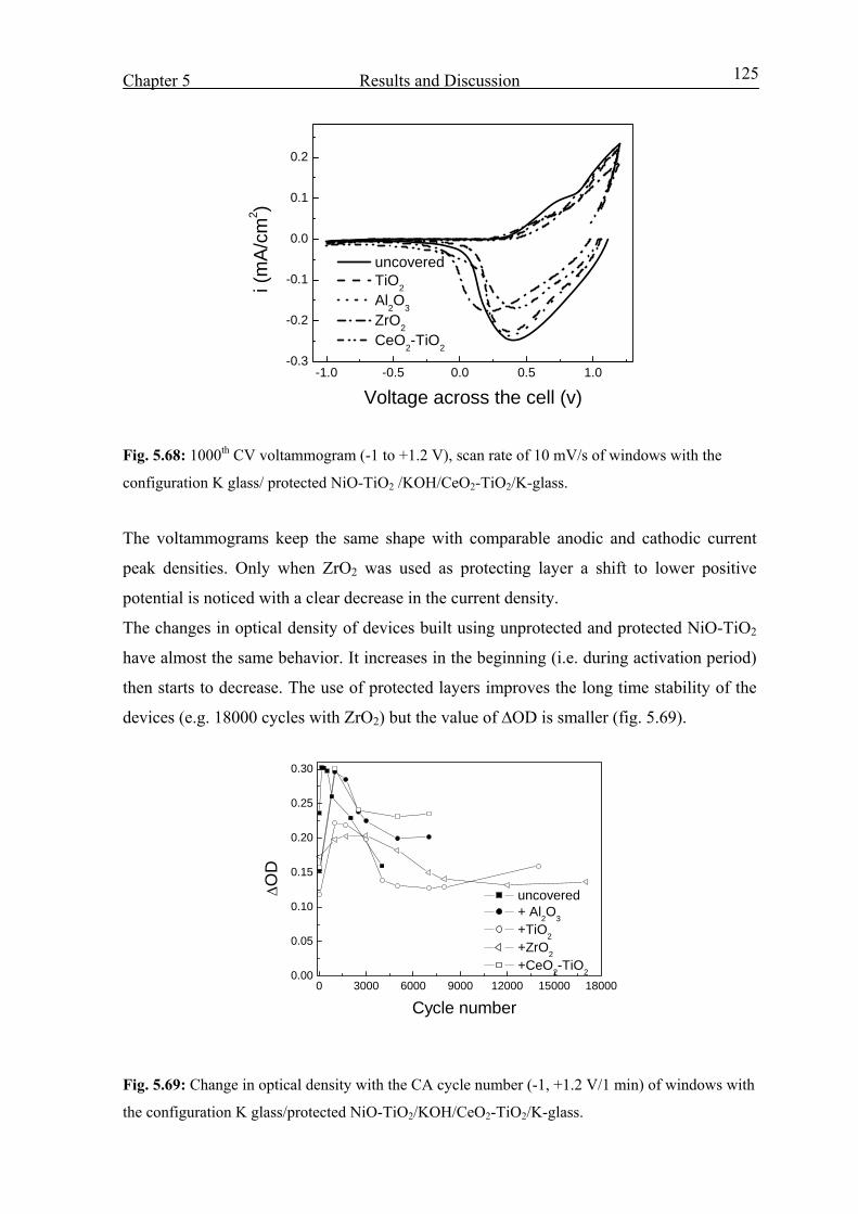
Chapter 5 Results and Discussion
125
-1.0 -0.5 0.0 0.5 1.0-0.3
-0.2
-0.1
0.0
0.1
0.2
uncovered TiO2 Al2O3 ZrO2 CeO2-TiO2
i (m
A/cm
2 )
Voltage across the cell (v)
Fig. 5.68: 1000th CV voltammogram (-1 to +1.2 V), scan rate of 10 mV/s of windows with the
configuration K glass/ protected NiO-TiO2 /KOH/CeO2-TiO2/K-glass.
The voltammograms keep the same shape with comparable anodic and cathodic current
peak densities. Only when ZrO2 was used as protecting layer a shift to lower positive
potential is noticed with a clear decrease in the current density.
The changes in optical density of devices built using unprotected and protected NiO-TiO2
have almost the same behavior. It increases in the beginning (i.e. during activation period)
then starts to decrease. The use of protected layers improves the long time stability of the
devices (e.g. 18000 cycles with ZrO2) but the value of ∆OD is smaller (fig. 5.69).
0 3000 6000 9000 12000 15000 180000.00
0.05
0.10
0.15
0.20
0.25
0.30
Cycle number
uncovered + Al2O3 +TiO2 +ZrO2 +CeO2-TiO2
ΔO
D
Fig. 5.69: Change in optical density with the CA cycle number (-1, +1.2 V/1 min) of windows with
the configuration K glass/protected NiO-TiO2/KOH/CeO2-TiO2/K-glass.
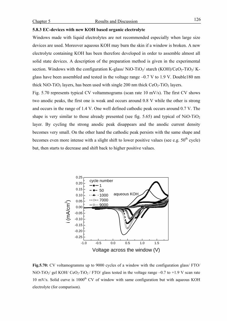
Chapter 5 Results and Discussion
126
5.8.3 EC-devices with new KOH based organic electrolyte
Windows made with liquid electrolytes are not recommended especially when large size
devices are used. Moreover aqueous KOH may burn the skin if a window is broken. A new
electrolyte containing KOH has been therefore developed in order to assemble almost all
solid state devices. A description of the preparation method is given in the experimental
section. Windows with the configuration K-glass/ NiO-TiO2/ starch (KOH)/CeO2-TiO2/ K-
glass have been assembled and tested in the voltage range –0.7 V to 1.9 V. Double180 nm
thick NiO-TiO2 layers, has been used with single 200 nm thick CeO2-TiO2 layers.
Fig. 5.70 represents typical CV voltammograms (scan rate 10 mV/s). The first CV shows
two anodic peaks, the first one is weak and occurs around 0.8 V while the other is strong
and occurs in the range of 1.4 V. One well defined cathodic peak occurs around 0.7 V. The
shape is very similar to those already presented (see fig. 5.65) and typical of NiO-TiO2
layer. By cycling the strong anodic peak disappears and the anodic current density
becomes very small. On the other hand the cathodic peak persists with the same shape and
becomes even more intense with a slight shift to lower positive values (see e.g. 50th cycle)
but, then starts to decrease and shift back to higher positive values.
-1.0 -0.5 0.0 0.5 1.0 1.5
-0.25
-0.20
-0.15
-0.10
-0.05
0.00
0.05
0.10
0.15
0.20
0.25
aqueous KOH
cycle number 1 50 1000 7000 9000
i (m
A/cm
2 )
Voltage across the window (V)
Fig.5.70: CV voltamogramms up to 9000 cycles of a window with the configuration glass/ FTO/
NiO-TiO2/ gel KOH/ CeO2-TiO2 / FTO/ glass tested in the voltage range –0.7 to +1.9 V scan rate
10 mV/s. Solid curve is 1000th CV of window with same configuration but with aqueous KOH
electrolyte (for comparison).
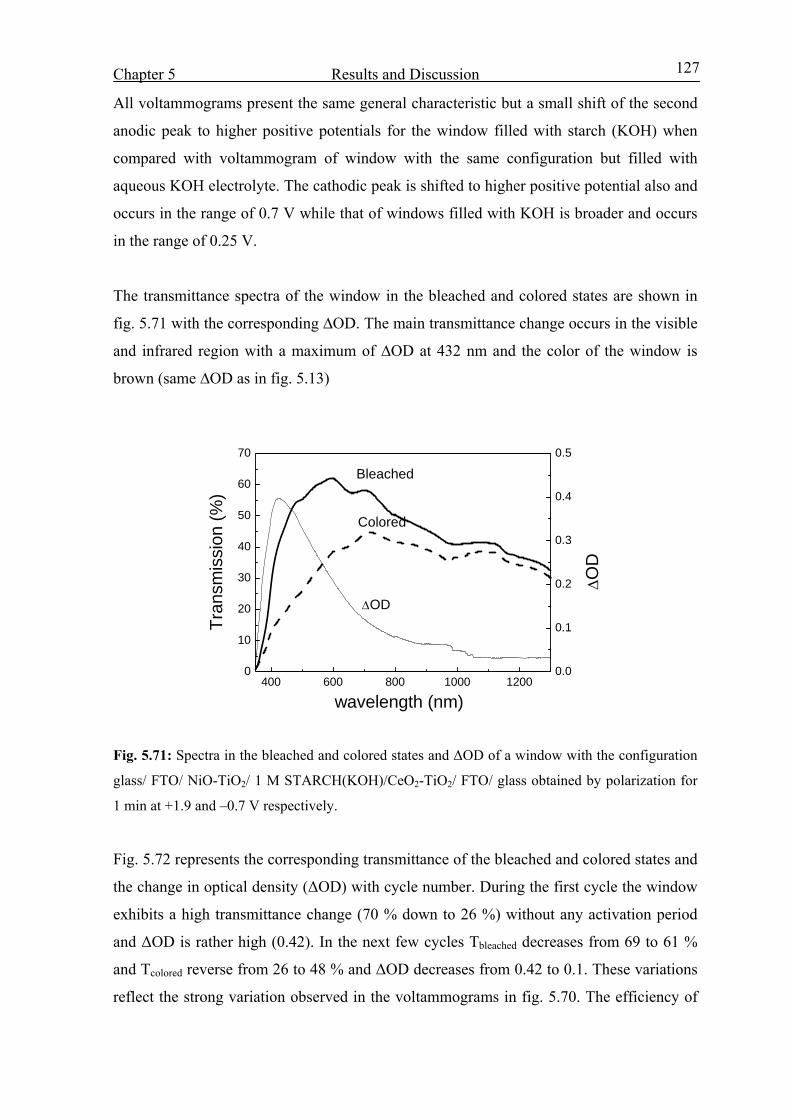
Chapter 5 Results and Discussion
127
All voltammograms present the same general characteristic but a small shift of the second
anodic peak to higher positive potentials for the window filled with starch (KOH) when
compared with voltammogram of window with the same configuration but filled with
aqueous KOH electrolyte. The cathodic peak is shifted to higher positive potential also and
occurs in the range of 0.7 V while that of windows filled with KOH is broader and occurs
in the range of 0.25 V.
The transmittance spectra of the window in the bleached and colored states are shown in
fig. 5.71 with the corresponding ∆OD. The main transmittance change occurs in the visible
and infrared region with a maximum of ∆OD at 432 nm and the color of the window is
brown (same ∆OD as in fig. 5.13)
400 600 800 1000 12000
10
20
30
40
50
60
70
0.0
0.1
0.2
0.3
0.4
0.5
Colored
ΔOD
Bleached
ΔOD
Tran
smis
sion
(%)
wavelength (nm)
Fig. 5.71: Spectra in the bleached and colored states and ΔOD of a window with the configuration
glass/ FTO/ NiO-TiO2/ 1 M STARCH(KOH)/CeO2-TiO2/ FTO/ glass obtained by polarization for
1 min at +1.9 and –0.7 V respectively.
Fig. 5.72 represents the corresponding transmittance of the bleached and colored states and
the change in optical density (ΔOD) with cycle number. During the first cycle the window
exhibits a high transmittance change (70 % down to 26 %) without any activation period
and ΔOD is rather high (0.42). In the next few cycles Tbleached decreases from 69 to 61 %
and Tcolored reverse from 26 to 48 % and ΔOD decreases from 0.42 to 0.1. These variations
reflect the strong variation observed in the voltammograms in fig. 5.70. The efficiency of

Chapter 5 Results and Discussion
128
the window improves again by cycling where ΔOD increases up to 0.27 after 2000 cycles
then starts to decrease again gradually.
Comparing the change in optical density. It is found that of the window filled with KOH
starts with a low ΔOD value (0.1) and increases gradually up to 0.29 after 4000 cycles
when corrosion of the layer starts. On the other hand ∆OD of windows filled with starch
(KOH) electrolyte is high initially (0.42), decrease in the initial cycles, but follow the same
behavior as that of the referee cell (filled with KOH) till 2000 cycles and then decreases.
0 2000 4000 6000 800020
30
40
50
60
70a
colored
bleached
Tran
smis
sion
(%)
Cycle number
0 2000 4000 6000 80000.00
0.05
0.10
0.15
0.20
0.25
0.30
0.35
0.40
0.45
b
aqueous KOH
starch (KOH)
ΔOD
cycle number
Fig. 5.72: (a) Transmittance of the bleached and colored states versus CA cycle number (-0.7,
1.9V/ 1min) of a window with the configuration K-glass/ NiO-TiO2/ Starch (KOH)/ CeO2-TiO2/ K-
glass. (b) Corresponding ΔOD of window, the dotted line is ΔOD of a window with same
configuration but filled with aqueous KOH electrolyte (for comparision).

Chapter 5 Results and Discussion
129
a) Kinetics
The kinetics of the coloration of the window is rather slow. In order to check if it is
possible to get deeper coloration, galvanostatic tests using different small currents (5, 10,
15 and 20 µA/cm2) have been made for different time periods keeping the total involved
charge of 13m C/cm2 and limiting the potential to maximum of +2 V.
0 10 20 30 400
10
20
30
40
50
60
20 µA/cm215 µA/cm2
10 µA/cm2
5 µA/cm2
Tran
smis
sion
(%)
Time (min)
Fig. 5.73: Evolution of the transmittance of windows with the configuration K-glass/ NiO-TiO2/
Starch (KOH)/ CeO2-TiO2/ K-glass during galvanostatic measurements performed using different
current densities.
The coloration kinetics get faster by increasing the current density applied to the window,
and the potential across the window did not exceed the secure level (2V) in all cases. The
fastest coloration was obtained by applying a current density of +20µA/cm2 and it took
11 min to reach a transmittance change from 60 % down to 33 % (ΔOD= 0.3).
b) Memory test
Window has been colored by polarizing it at the positive potential (+1.9V) for 1 min. The
transmittance was then measured in open circuit to check the memory of the window i.e. to
get the evolution of the transmittance of the colored window. The result is shown in
fig. 5.74. The window transmittance increases from 39 % to 49 % after 1 hour.
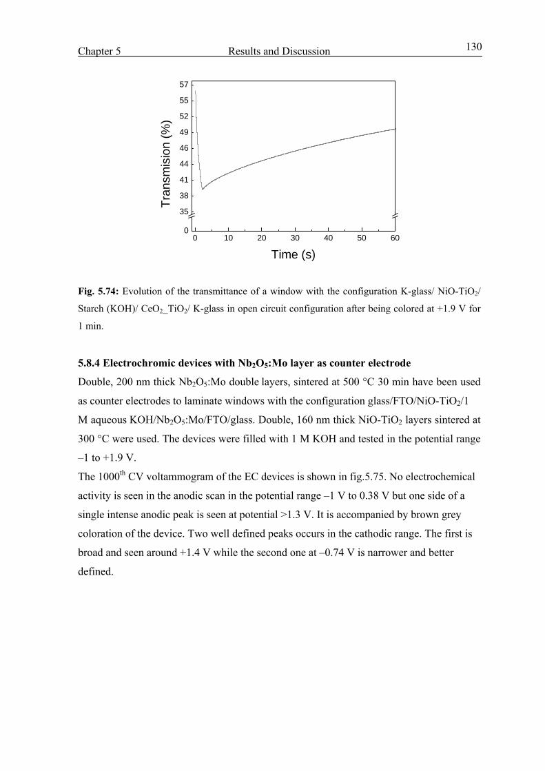
Chapter 5 Results and Discussion
130
0 10 20 30 40 50 600
35
38
41
44
46
49
52
55
57
Tran
smis
ion
(%)
Time (s)
Fig. 5.74: Evolution of the transmittance of a window with the configuration K-glass/ NiO-TiO2/
Starch (KOH)/ CeO2_TiO2/ K-glass in open circuit configuration after being colored at +1.9 V for
1 min.
5.8.4 Electrochromic devices with Nb2O5:Mo layer as counter electrode
Double, 200 nm thick Nb2O5:Mo double layers, sintered at 500 °C 30 min have been used
as counter electrodes to laminate windows with the configuration glass/FTO/NiO-TiO2/1
M aqueous KOH/Nb2O5:Mo/FTO/glass. Double, 160 nm thick NiO-TiO2 layers sintered at
300 °C were used. The devices were filled with 1 M KOH and tested in the potential range
–1 to +1.9 V.
The 1000th CV voltammogram of the EC devices is shown in fig.5.75. No electrochemical
activity is seen in the anodic scan in the potential range –1 V to 0.38 V but one side of a
single intense anodic peak is seen at potential >1.3 V. It is accompanied by brown grey
coloration of the device. Two well defined peaks occurs in the cathodic range. The first is
broad and seen around +1.4 V while the second one at –0.74 V is narrower and better
defined.

Chapter 5 Results and Discussion
131
-1.0 -0.5 0.0 0.5 1.0 1.5
-0.1
0.0
0.1
0.2
0.3
i (m
A/cm
2 )
V across the window (V)
Fig. 5.75: 1000th CV voltammograms (-1 to +1.9 V) scan rate of 10mV/s of a window with the
configuration K glass/ NiO-TiO2/ 1 M KOH/Nb2O5:Mo/ K-glass with double NiO-TiO2 and
Nb2O5:Mo layers.
The transmittance spectra of the device in the bleached and colored states and the
corresponding ΔOD are shown in fig. 5.76. The main transmittance change occurs in the
visible range with a broad maximum of ΔOD between 390 and 440 nm The spectra look
very similar to that of devices with the same configuration but using CeO2-TiO2 counter
electrode (see fig. 5.58) but the transmittance of the bleached state is a little smaller in the
visible range and the maximum of ΔOD is broader.
400 500 600 700 800 900 1000 1100 1200 13000
10
20
30
40
50
60
70
0.0
0.1
0.2
0.3
0.4
ΔOD
trans
mis
sion
(%)
Wavelength (nm)
ΔOD
T bleached
Tcolored
Fig. 5.76: Transmittance in the bleached and colored states of a windows with the configuration
glass/ FTO/NiO-TiO2/ 1 M liquid KOH/ Nb2O5:Mo/ FTO/ glass. It was colored and bleached by
polarizing for 1 min at +1.9 V and –1 V respectively. The dotted curve is the corresponding ΔOD.
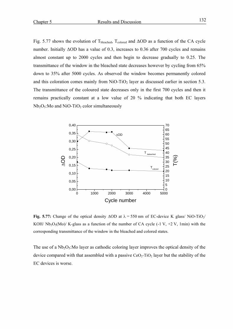
Chapter 5 Results and Discussion
132
Fig. 5.77 shows the evolution of Tbleached, Tcolored and ΔOD as a function of the CA cycle
number. Initially ΔOD has a value of 0.3, increases to 0.36 after 700 cycles and remains
almost constant up to 2000 cycles and then begin to decrease gradually to 0.25. The
transmittance of the window in the bleached state decreases however by cycling from 65%
down to 35% after 5000 cycles. As observed the window becomes permanently colored
and this coloration comes mainly from NiO-TiO2 layer as discussed earlier in section 5.3.
The transmittance of the coloured state decreases only in the first 700 cycles and then it
remains practically constant at a low value of 20 % indicating that both EC layers
Nb2O5:Mo and NiO-TiO2 color simultaneously
0 1000 2000 3000 4000 50000,00
0,05
0,10
0,15
0,20
0,25
0,30
0,35
0,40
0510152025303540455055606570
T(%
)
ΔOD
T beleached
Tcolored
ΔOD
Cycle number
Fig. 5.77: Change of the optical density ΔOD at λ = 550 nm of EC-device K glass/ NiO-TiO2/
KOH/ Nb2O5(Mo)/ K-glass as a function of the number of CA cycle (-1 V, +2 V, 1min) with the
corresponding transmittance of the window in the bleached and colored states.
The use of a Nb2O5:Mo layer as cathodic coloring layer improves the optical density of the
device compared with that assembled with a passive CeO2-TiO2 layer but the stability of the
EC devices is worse.
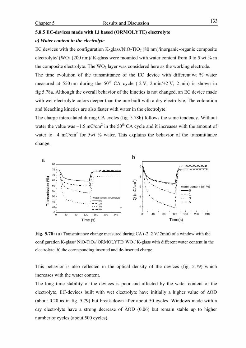
Chapter 5 Results and Discussion
133
5.8.5 EC-devices made with Li based (ORMOLYTE) electrolyte
a) Water content in the electrolyte
EC devices with the configuration K-glass/NiO-TiO2 (80 nm)/inorganic-organic composite
electrolyte/ (WO3 (200 nm)/ K-glass were mounted with water content from 0 to 5 wt.% in
the composite electrolyte. The WO3 layer was considered here as the working electrode.
The time evolution of the transmittance of the EC device with different wt % water
measured at 550 nm during the 50th CA cycle (-2 V, 2 min/+2 V, 2 min) is shown in
fig 5.78a. Although the overall behavior of the kinetics is not changed, an EC device made
with wet electrolyte colors deeper than the one built with a dry electrolyte. The coloration
and bleaching kinetics are also faster with water in the electrolyte.
The charge intercalated during CA cycles (fig. 5.78b) follows the same tendency. Without
water the value was –1.5 mC/cm2 in the 50th CA cycle and it increases with the amount of
water to –4 mC/cm2 for 5wt % water. This explains the behavior of the transmittance
change.
0 40 80 120 160 200 2400
40
45
50
55
60
65
70
75
80a
Water content in Ormolyte 0% 1% 3% 5%
Tran
smis
sion
(%)
Time (s)0 40 80 120 160 200 240
-4
-3
-2
-1
0
b
water content (wt %) 0 1 3 5
Q (m
C/c
m2 )
Time(s)
Fig. 5.78: (a) Transmittance change measured during CA (-2, 2 V/ 2min) of a window with the
configuration K-glass/ NiO-TiO2/ ORMOLYTE/ WO3/ K-glass with different water content in the
electrolyte, b) the corresponding inserted and de-inserted charge.
This behavior is also reflected in the optical density of the devices (fig. 5.79) which
increases with the water content.
The long time stability of the devices is poor and affected by the water content of the
electrolyte. EC-devices built with wet electrolyte have initially a higher value of ∆OD
(about 0.20 as in fig. 5.79) but break down after about 50 cycles. Windows made with a
dry electrolyte have a strong decrease of ∆OD (0.06) but remain stable up to higher
number of cycles (about 500 cycles).
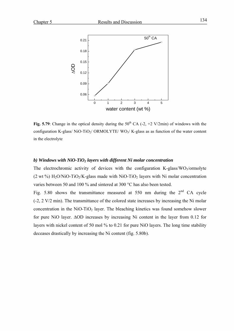
Chapter 5 Results and Discussion
134
0 1 2 3 4 5
0.06
0.09
0.12
0.15
0.18
0.21
50th CA
ΔOD
water content (wt %)
Fig. 5.79: Change in the optical density during the 50th CA (-2, +2 V/2min) of windows with the
configuration K-glass/ NiO-TiO2/ ORMOLYTE/ WO3/ K-glass as as function of the water content
in the electrolyte
b) Windows with NiO-TiO2 layers with different Ni molar concentration
The electrochromic activity of devices with the configuration K-glass/WO3/ormolyte
(2 wt %) H2O/NiO-TiO2/K-glass made with NiO-TiO2 layers with Ni molar concentration
varies between 50 and 100 % and sintered at 300 °C has also been tested.
Fig. 5.80 shows the transmittance measured at 550 nm during the 2nd CA cycle
(-2, 2 V/2 min). The transmittance of the colored state increases by increasing the Ni molar
concentration in the NiO-TiO2 layer. The bleaching kinetics was found somehow slower
for pure NiO layer. ∆OD increases by increasing Ni content in the layer from 0.12 for
layers with nickel content of 50 mol % to 0.21 for pure NiO layers. The long time stability
deceases drastically by increasing the Ni content (fig. 5.80b).

Chapter 5 Results and Discussion
135
0 50 100 150 200 25040
50
60
70
80a
1007566
50
Tran
smis
sion
(%)
Time (s)0 200 400 600 800 1000 1200 1400 1600 1800 2000
0.00
0.03
0.06
0.09
0.12
0.15
0.18
0.21
0.24
100
7566
50
ΔOD
Cycle number
Fig. 5.80: (a) Transmittance measured at 550 nm during 2nd CA (-2, +2 V/2min) of windows with
the configuration K-glass/ NiO-TiO2/ ORMOLYTE (2wt % H2O)/ WO3/ K-glass. NiO-TiO2 layers
have ben prepared with different Ni molar concentration. (b) Change in optical density as a
function of cycle number.
Chapter 6 Summary and Conclusion
136
Chapter 6 Summary and Conclusion
NiO-TiO2 xerogels and layers have been prepared by the sol-gel route with several Ni
molar concentrations. Transparent single and multiple layers with total thickness up to
240 nm have been deposited on FTO coated glass by dip-coating and sintered up to
500 °C.
Thermal analysis of xerogels has been performed using simultaneous DTA-TG coupled to
mass and infrared spectroscopy. A mass loss of about 10 wt% accompanied by an H2O
evolution was detected by MS and FTIR spectroscopy below 200 °C, corresponding to a
final drying of the layer. The main feature of the DTA curve was a strong exothermic
double peak between 300 and 360 °C with maximum at 344 and 357 °C. These features
were accompanied by a large two peaks mass loss of about 35 wt %. A careful analysis of
the infrared spectra of the gases evolved at these temperature values shows that the
formation of inorganic nickel compounds, involving primarily NiOx and possibly NiCO3,
only occurs up to about 350 °C. The last peak at 357 °C corresponds to the transformation
of NiCO3 into NiO.
SEM pictures of the coatings made with different Ni molar concentration indicated that all
layers were homogeneous without pits or cracks. All coatings showed a slight greenish
color.
Sol-gel NiO-TiO2 layers sintered at different temperatures up to 500 °C had the Bunsenite
cubic NiO structure regardless of the Ni concentration. The crystallinity of the layers
increased with the sintering temperature and the crystallite size calculated with the (200)
peak were 2.5, 4.7 and 8 nm after sintering at 300, 400, 500 °C respectively.
The electrochromic properties of the layers have been tested using cyclic voltammetry and
chronoamperometry in 1 M aqueous solution of KOH as a function of the potential range,
of the Ni content, of the heat treatment and of the thickness. Pure NiO layers showed a
poor adhesion to the substrate, a permanent brown coloration after already 50 CV cycles
and were easily degraded in the electrolyte. The adhesion was clearly improved by
increasing the Ti content. For example the transmittance in the bleached state remained
high and constant (> 75 %) up to 400 cycles when the Ni molar concentration was
Chapter 6 Summary and Conclusion
137
<85 mol %. However both the optical density and the charge capacity decreased
continuously by increasing the Ti content. The layers that presented the best properties
were 160 nm thick double layers having a Ni molar concentration of 75 mol % and sintered
between 300 and 350 °C. When cycled between –0.6 and +1 V vs. SCE, they showed a
deep reversible brown coloration with change of transmittance at 550 nm between 90 and
25 %, an extended stability of about 2000 cycles and a fast switching time <10 s. The
coloration of NiO-TiO2 initiates in a thin interface layer (about 40-50 nm) that grows with
cycling till reaching the full depth of the layer at the end of a so-called activation period
that lasts up to about 1000 cycles depending on the potential range, the thickness of the
layer and the sintering temperature. Simultaneously a slow degradation period takes place
in which a passive, irreversible colored and very fragile layer is formed. This period is
clearly observed after about 1000 cycles in which both the exchanged charge and the
transmittance in the bleached state and correspondingly the change in optical density
decrease. Due to the extreme fragility of this passive layer, the NiO-TiO2 is also gradually
disaggregated into the electrolyte till the layer is completely removed from the substrate
after about 7000 to 10000 cycles.
The coloration mechanism of NiO-TiO2 layers in KOH electrolyte was studied using a
quartz crystal microbalance (QCM) in the potential range –0.4 to +0.57 V vs. SCE. Models
have been suggested and discussed. The increase of the current density, charge and mass
with cycling are compatible with the ideas proposed earlier that, in this activation period,
only a thin layer located at the interface electrolyte/layer is active and that the thickness of
this layer increases by cycling. Without knowing with precision the complex surroundings
of the NiO nanoparticles, where the presence of Ni(OH)2 (not observed by X-ray) and H2O
too is expected because of the low sintering temperature and/or by the wetting of the layer
in the electrolyte, it is not possible to precisely assign a model. One possible equation to
describe the results for E> 0.35 V is
Ni(OH)2 + OH- ↔ (NiOOH).(y/x)H2O + (1-(y/x)) H2O+ e-
with 0 ≤ y≤ x+1
This formula describes the bonding of hydroxyls ions to Ni(OH)2 with formation of
hydrated NiOOH giving rise to the coloration of the film, the equation suggesting also the
formation of lattice water.
The irreversible increase of both the mass and charge exchanged during each cycle was
interpreted to be due to an increase of the amount of Ni(OH)2 according to
Chapter 6 Summary and Conclusion
138
NiO+z H2O → Ni(OH)2 + (1-z)NiO
This allowed to understand the increase of the coloration behavior of the layer and the
change of its morphology as observed by the TEM measurement.
This gradual change of the morphology lead also to a more open and mechanically fragile
structure so that unusual large increase of the mass of the layer during each cycle has been
observed eventually after the 330 cycles. This was interpreted as due to the incorporation
of K+ ions and water that led to the degradation period.
The electrochromic properties of the layers have been also tested in the three electrode cell
filled with a LiClO4-PC using Ag/AgClO4-PC as reference electrode. It was proposed that
the EC process involving a cathodic charge of up to 9 mC/cm2 (for 80 nm thick film) was
linked to an irreversible compositional changes of Ni(OH)2 with the decomposition of
small amount of water remaining in the layer. At more negative potentials Li+ together
with e- can be effectively incorporated cathodically into the layer and the composition of
the layer continuously changed to LizNiO-TiO2. The electron may be localized by
interacting with Ni2+ or most likely with the defects containing Li+ or delocalized giving
rise to the formation of polarons. In this case a mechanism similar to that of cathodic
electrochromic materials like WO3 and Nb2O5 is observed and the layer became colored.
By reversing the galvanostatic current but limiting the potential to 0 V or during an anodic
scan between–2.4 to 0 V, Li+ ions are deinserted slowly out of the layer. Depending on the
current and involved charge the layer may not be bleached completely, so that by further
cycling, the composition of the layer oscillates between a partially transparent LiaNiO-
TiO2 and a colored LibNiO-TiO2 where b> a.
Brown coloring electrochromic devices have been built using NiO-TiO2 layers with the
configuration glass/FTO/NiO-TiO2 (160 nm)/1 M liquid KOH/CeO2-TiO2 /FTO/ glass. The
change in optical density of the device was in the range of 0.3 with coloration efficiency of
about 41 cm2/C. The window gained a permanent brown color by cycling due to the
permanent coloration of NiO-TiO2 layer. The long term stability of the devices was
improved to 7000 cycles by using double NiO-TiO2 layers instead of single layers (4000
cycles).
Chapter 6 Summary and Conclusion
139
By depositing thin layers of dielectric oxides such as ZrO2, TiO2, Al2O3 and CeO2-TiO2
(all 20 to 25 nm thick) on top of the NiO-TiO2 layer, the corrosion resistance in KOH
electrolyte was improved so that long time stability up to 17000 cycles could be obtained.
Electrochromic devices using Nb2O5:Mo as cathodic counter electrode instead of the
passive CeO2-TiO2 with the configuration glass/ FTO/ NiO-TiO2 (160 nm)/ 1 M
aqueous KOH/ Nb2O5:Mo (200 nm)/ FTO/ glass have been also tested in the potential
range –1 to 1.9 V. the colored state of these devices were grey-brown. The use of a
Nb2O5:Mo layer improved the change in optical density of the device (0.36) but their
stability was worsened (5000 cycles only).
A new gel electrolyte containing KOH has been also developed to assemble almost all
solid state devices. Windows with the configuration K-glass/ NiO-TiO2/ starch (KOH)/
CeO2-TiO2/ K-glass have been assembled and tested in the voltage range –0.7 V to +1.9 V.
During the first cycles the window exhibits a high transmittance change (70 % down to
26 %) without any activation period and ΔOD was rather high (0.42). In the next few
cycles Tbleached decreased from 69 to 61 % and Tcolored reversed from 26 to 48 % so that
ΔOD decreased from 0.42 to 0.1. The efficiency of the window was improved again by
cycling and ΔOD value up to 0.27 have been obtained after 2000 cycles.

Appendices
140
Appendices
A.1 Optimisation of dip-coating soaking time The effect of the time period during which the substrate remains in the sol during the dip
coating process was tested by varying it between 15 and 240 s. The thickness of the layers
was not affected.
However for period of time longer than 60 s, the layer was found hazy and not
homogeneous. The change in optical density and in the charge capacity for layers soaked
for different period of times are shown in fig.A.1
0.00
0.32
0.34
0.36
0.38
0.40
20 40 60 80 100 1200
10
11
12
13
14
Qc (
mC
/cm
2 )
Qc (mC/cm2)
ΔOD
ΔOD
Soaking time (s)
Fig. A.1: Charge capacity and change in optical density calculated from CV recording (-0.6 to
+1 V) in KOH for NiO-TiO2 layers (Ni molar concentration of 75 m %) deposited by dip coating
technique with different soaking time and then sintered at 300 °C.
The change in optical density and the charge capacity decrease slightly by increasing the
soaking time. 15 s was found an optimum

Appendices
141
A.2 XPS spectrum Studies realized with NiO based systems have always given very complex XPS spectra
where the O 1s peaks bounded to Ni2+ and Ni3+ also Ni 2p3/2 peaks coming from Ni2+ and
Ni3+ are overlapped [210].
The composition of NiO-TiO2 layer in the colored and uncolored states was tested by XPS
spectroscopy. An M-Probe (SSI surface science) spectrometer with Al-Kα 1486.6 eV
monochromatic radiation was used. For sputter depth profiling, an Ar+ beam of 2.5 KV
was used to bombard an area of 2x2 mm2 during 60s in 15x10-8 mbar vacuum.
The XPS spectra were recorded in the range 5 to 1000 eV for fresh and colored layer. The
O 1s and Ni 2p3/2 results are shown in fig. A.2 and A.3 respectively. The energy scale was
corrected with respect to the position of C 1s peak at 284.8 eV.
540 538 536 534 532 530 528 526 5240
4000
8000
12000
16000
20000
24000
as-deposited
colored
531.7eV O1s linked to NiOOH
529.7 eV O1s linked to NiO
Inte
nsity
(a. u
.)
Binding energy (eV)
Fig. A.2 : O 1s spectrum at the surface of as-deposited and colored NiO-TiO2 layers (Ni molar
concentration of 75 mol. %) sintered at 300 °C. The layer was colored by cycling in a three
electrode cell in KOH electrolyte for 50 CV cycles (-0.6 to +1 V) and disconnected in the colored
state at +1 V. The values in the graphs are from literature [21].
O 1s states in nickel oxide compounds give one single peak centred at 529.7 for
stoichiometric NiO (Ni2+) and at 531.3, 531.7 eV in hydrogen containing phases Ni(OH)2
(Ni2+) and NiOOH (Ni3+) respectively [21].
The overall width of the intensity vs. binding energy is much larger than that published in
the literature (usually FWHM =1-1.5 eV). This may come from an instrument artifact but
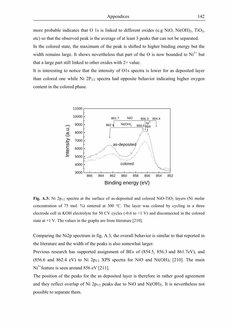
Appendices
142
more probable indicates that O 1s is linked to different oxides (e.g NiO, Ni(OH)2, TiO2,
etc) so that the observed peak is the average of at least 3 peaks that can not be separated.
In the colored state, the maximum of the peak is shifted to higher binding energy but the
width remains large. It shows nevertheless that part of the O is now bounded to Ni3+ but
that a large part still linked to other oxides with 2+ value.
It is interesting to notice that the intensity of O1s spectra is lower for as deposited layer
than colored one while Ni 2P3/2 spectra had opposite behavior indicating higher oxygen
content in the colored phase.
866 864 862 860 858 856 854 8523000
4000
5000
6000
7000
8000
9000
10000
11000
colored
856
NiO
856.6
861.7 854.4Ni3+
as-deposited
856.3
Ni(OH)2862.4
Inte
nsity
(a.u
.)
Binding energy (eV)
Fig. A.3: Ni 2p3/2 spectra at the surface of as-deposited and colored NiO-TiO2 layers (Ni molar
concentration of 75 mol. %) sintered at 300 °C. The layer was colored by cycling in a three
electrode cell in KOH electrolyte for 50 CV cycles (-0.6 to +1 V) and disconnected in the colored
state at +1 V. The values in the graphs are from literature [210].
Comparing the Ni2p spectrum in fig. A.3, the overall behavior is similar to that reported in
the literature and the width of the peaks is also somewhat larger.
Previous research has supported assignment of BEs of (854.5, 856.3 and 861.7eV), and
(856.6 and 862.4 eV) to Ni 2p3/2 XPS spectra for NiO and Ni(OH)2 [210]. The main
Ni3+feature is seen around 856 eV [211].
The position of the peaks for the as deposited layer is therefore in rather good agreement
and they reflect overlap of Ni 2p3/2 peaks due to NiO and Ni(OH)2. It is nevertheless not
possible to separate them.
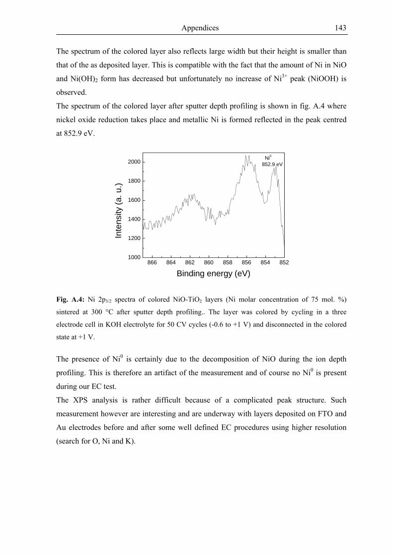
Appendices
143
The spectrum of the colored layer also reflects large width but their height is smaller than
that of the as deposited layer. This is compatible with the fact that the amount of Ni in NiO
and Ni(OH)2 form has decreased but unfortunately no increase of Ni3+ peak (NiOOH) is
observed.
The spectrum of the colored layer after sputter depth profiling is shown in fig. A.4 where
nickel oxide reduction takes place and metallic Ni is formed reflected in the peak centred
at 852.9 eV.
866 864 862 860 858 856 854 8521000
1200
1400
1600
1800
2000 Ni0
852.9 eV
Inte
nsity
(a. u
.)
Binding energy (eV)
Fig. A.4: Ni 2p3/2 spectra of colored NiO-TiO2 layers (Ni molar concentration of 75 mol. %)
sintered at 300 °C after sputter depth profiling.. The layer was colored by cycling in a three
electrode cell in KOH electrolyte for 50 CV cycles (-0.6 to +1 V) and disconnected in the colored
state at +1 V.
The presence of Ni0 is certainly due to the decomposition of NiO during the ion depth
profiling. This is therefore an artifact of the measurement and of course no Ni0 is present
during our EC test.
The XPS analysis is rather difficult because of a complicated peak structure. Such
measurement however are interesting and are underway with layers deposited on FTO and
Au electrodes before and after some well defined EC procedures using higher resolution
(search for O, Ni and K).
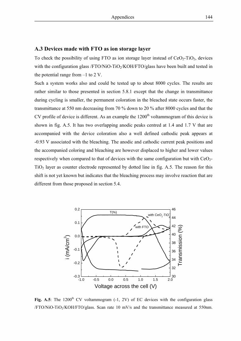
Appendices
144
A.3 Devices made with FTO as ion storage layer To check the possibility of using FTO as ion storage layer instead of CeO2-TiO2, devices
with the configuration glass /FTO/NiO-TiO2/KOH/FTO/glass have been built and tested in
the potential range from –1 to 2 V.
Such a system works also and could be tested up to about 8000 cycles. The results are
rather similar to those presented in section 5.8.1 except that the change in transmittance
during cycling is smaller, the permanent coloration in the bleached state occurs faster, the
transmittance at 550 nm decreasing from 70 % down to 20 % after 8000 cycles and that the
CV profile of device is different. As an example the 1200th voltammogram of this device is
shown in fig. A.5. It has two overlapping anodic peaks centred at 1.4 and 1.7 V that are
accompanied with the device coloration also a well defined cathodic peak appears at
-0.93 V associated with the bleaching. The anodic and cathodic current peak positions and
the accompanied coloring and bleaching are however displaced to higher and lower values
respectively when compared to that of devices with the same configuration but with CeO2-
TiO2 layer as counter electrode represented by dotted line in fig. A.5. The reason for this
shift is not yet known but indicates that the bleaching process may involve reaction that are
different from those proposed in section 5.4.
-1.0 -0.5 0.0 0.5 1.0 1.5 2.0-0.3
-0.2
-0.1
0.0
0.1
0.2
30
32
34
36
38
40
42
44
46T(%)
Tran
smis
sion
(%)with FTO
with CeO2-TiO2
i (m
A/cm
2 )
Voltage across the cell (V)
Fig. A.5: The 1200th CV voltammogram (-1, 2V) of EC devices with the configuration glass
/FTO/NiO-TiO2/KOH/FTO/glass. Scan rate 10 mV/s and the transmittance measured at 550nm.
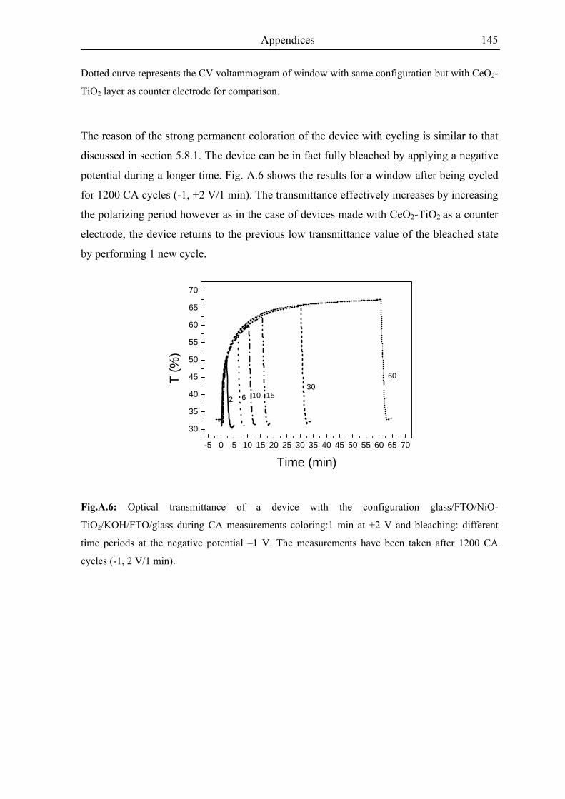
Appendices
145
Dotted curve represents the CV voltammogram of window with same configuration but with CeO2-
TiO2 layer as counter electrode for comparison.
The reason of the strong permanent coloration of the device with cycling is similar to that
discussed in section 5.8.1. The device can be in fact fully bleached by applying a negative
potential during a longer time. Fig. A.6 shows the results for a window after being cycled
for 1200 CA cycles (-1, +2 V/1 min). The transmittance effectively increases by increasing
the polarizing period however as in the case of devices made with CeO2-TiO2 as a counter
electrode, the device returns to the previous low transmittance value of the bleached state
by performing 1 new cycle.
-5 0 5 10 15 20 25 30 35 40 45 50 55 60 65 70
30
35
40
45
50
55
60
65
70
2 6 10 1530
60
T (%
)
Time (min)
Fig.A.6: Optical transmittance of a device with the configuration glass/FTO/NiO-
TiO2/KOH/FTO/glass during CA measurements coloring:1 min at +2 V and bleaching: different
time periods at the negative potential –1 V. The measurements have been taken after 1200 CA
cycles (-1, 2 V/1 min).

Appendices
146
B) List of chemicals used in this work:
Chemicals Symbol Supplier Purity (%)
Nickel acetate tetrahydrate
Ni(CH3COO)2.4H2O Fluka 99+
Titanium n-propoxide
Ti(C3H7O)4 Heraeus ≥90
Cerium (III)nitrate hexahydrate
Ce(NO3)3⋅6H2O Chempur 99.9
Phosphomolybdic acid hydrate
H3[P(Mo3O10)4]٠ Kluka ≥98.5
Niobium(V) chloride
NbCl5 Chempur 99+
glycidoxypropyltrimethoxysilane (GPTS),
C9H20O5Si ABCR ≥98
Lithium perchlorate LiClO4 Fluka ≥98 zirconium (IV) n-propoxide
Zr(OC3H7)4 Chempur 70 %
solution tetraethylene glycol (TEG) HO(CH2CH2O)3CH2CH
2OH Acros
Organics ≥99.5
propylene carbonate
C4H6O3 Fluka Puriss: ≥99
Silver perchlorate AgClO4 RdH ≥98.5
Aluminium tri-sec butylate C12H27AlO3 MERCK-Schuchard
Al >97
Starch from maize
(C6H10O5)n Fluka
Glycerol
C3H8O3 Fluka Assay >99.5
Formaldehyde CH2O Fluka Assay >36.5 in
water Potassium hdroxide KOH Fluka Assay
>98.5 Sodium hydroxide NaOH Fluka Assay >97 Lithium hydroxide LiOH Fluka Assay >97
Tetrabutylammonium hdroxide C16H36NOH Sigma-Aldrich 1 M in water
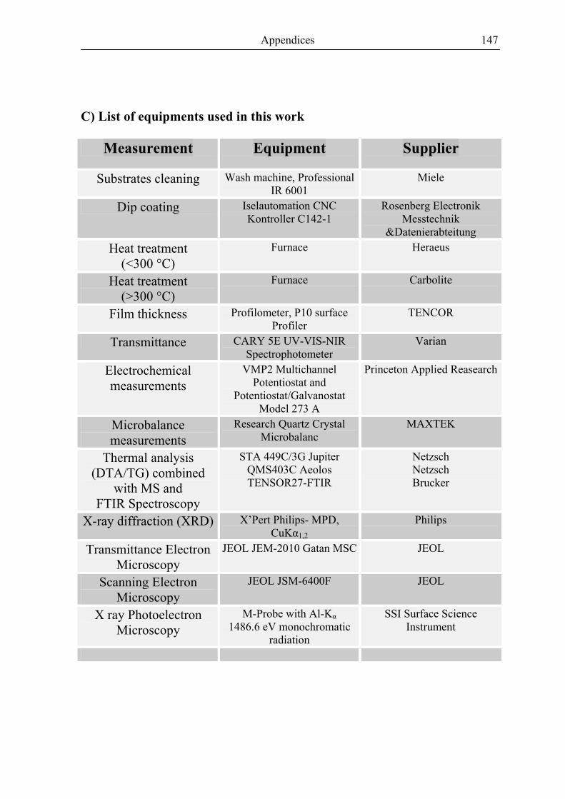
Appendices
147
C) List of equipments used in this work
Measurement Equipment Supplier
Substrates cleaning Wash machine, Professional IR 6001
Miele
Dip coating Iselautomation CNC Kontroller C142-1
Rosenberg Electronik Messtechnik
&Datenierabteitung Heat treatment
(<300 °C) Furnace Heraeus
Heat treatment (>300 °C)
Furnace Carbolite
Film thickness Profilometer, P10 surface Profiler
TENCOR
Transmittance CARY 5E UV-VIS-NIR Spectrophotometer
Varian
Electrochemical measurements
VMP2 Multichannel Potentiostat and
Potentiostat/Galvanostat Model 273 A
Princeton Applied Reasearch
Microbalance measurements
Research Quartz Crystal Microbalanc
MAXTEK
Thermal analysis (DTA/TG) combined
with MS and FTIR Spectroscopy
STA 449C/3G Jupiter QMS403C Aeolos TENSOR27-FTIR
Netzsch Netzsch Brucker
X-ray diffraction (XRD) X’Pert Philips- MPD, CuKα1,2
Philips
Transmittance Electron Microscopy
JEOL JEM-2010 Gatan MSC JEOL
Scanning Electron Microscopy
JEOL JSM-6400F JEOL
X ray Photoelectron Microscopy
M-Probe with Al-Kα 1486.6 eV monochromatic
radiation
SSI Surface Science Instrument
References
148
References 1. C.M. Lampert, Materials Today, 7 (2004) 28. 2. J.P. Cronin, T.J. Gudgel, S.R. Kennedy, A. Agrawal, D.R. Uhlmann, Material
Research., 2 (1999) 1. 3. N.A. O'brien, J.Gordon, H. Mathew, B.P. Hichwa, Thin solid films, 345 (1999) 312. 4. A. Azens, E. Avendaño, J. Backholm, L. Berggren, G. Gustavsson, R. Karmhag,
G.A. Niklasson, A. Roos, C.G. Granqvist, Materials Science and Engineering B, 119 (2005) 214.
5. C.G. Granqvist, Journal of the European Ceramic Society, 25 (2005) 2907. 6. H. Dislich, Noyes Publications, (1988) 51. 7. H. Schmidt, In sol-gel optics: proceeding and applications ed by L.Klein,
Dordrecht: kluwer (1994) 451. 8. K.A. Mauritz, R.M. Warren, Macromolecules, 22 (1989) 1730. 9. L.L. Hench, J.K. West, Chem. Rev., 90 (1990) 33. 10. H. Schmidt, Sol-Gel Scienece and Technology, 14-19 (1989) 61. 11. C.J. Brinker, G.W. Scherer, chapter 2, Academic Press, Inc. (1990). 12. S.V. Davis, K.A. Mauritz, Am. Chem. Soc. Polym. Preperation, 34 (1993) 608. 13. J. Puetz, M.A. Aegerter, Dip Coating techniques in M.A. Aegerter and M. Menig
(eds) Handbook on sol-gel techniques for glass users and producers, Veröffentlichung (2004).
14. H.K Schmidt., Macromolecular Symposium, 101 (1996) 333. 15. N. Al-Dahoudi, PhD Thesis, Leibnitz Institute for New Materials (INM) and
University of Saarland, Saarbruecken, Germany (2003) 13. 16. Http://Homepage.Ntlworld.Com/Colin.Pratt/Chromism.Pdf, 17. P.M.S. Monk, S.P. Akhtar, J. Boutevin, J.R. Duffield, Electrochimica Acta, 46
(2001) 2091. 18. G.A. Niklassona, L. Berggrena, A. Jonssona, R. Ahujab N.V. Skorodumovab, J.
Backholma, M. Strømmea, Solar Energy Materials & Solar Cells, 90 (2006) 385. 19. P.M.S. Monk, R.J. Mortimer, D.R. Rosseinsky, Electrochromism: Fundamentals
and Applications. (1995) Weinheim, VCH. 20. C.G. Granqvist, Handbook of Inorganic Electrochromic Materials. (1995)
Amsterdam, Elsevier.
References
149
21. E. Avendano, Uppsala Dissertation from the faculty of science and technology
(56), (2004). 22. Http://Library.Kcc.Hawaii.Edu/External/Chemistry/Everyday_Electro.Html, 23. P.R. Somani, S. Radhakrishnan, Materials Chemistry and Physics, 77 (2002) 117. 24. J. Livage, D. Ganguli, Solar Energy Materials & Solar Cells, 84 (2004) 315. 25. S. Radhakrisnan, S. Unde, A.B. Mandale, Materials Chemistry and Physics, 48
(1997) 268. 26. M. Ohyama, H. Kozuka, T. Yoko, J. Am. Ceram. Soc., 81 (1998) 1622. 27. S.F. Corgan, T.D. Plante, M.A. Parker, R.D. Rauh, Solar Energy Materials, 14
(1986) 185. 28. J.S.E.M. Svensson, C.G. Granqvist, Thin Solid Films, 126 (1985) 31. 29. C.G. Granqvist, J Solar Energy Materials and Solar Cells, 60 (2000) 201. 30. J.P. Cronin, D.J. Tarico, J.C.L. Tonazzi, A. Agrawal, S.R. Kennedy, Solar Energy
Materials & Solar Cells, 29 (1993) 371. 31. J. Nagai, T. Kamimori, M. Mizuhashi, Proc. SPIE, 502 (1984) 59. 32. A. Deneuvillea, P. Gérarda, R. Billata, Thin Solid Films, 70 (1980) 203. 33. P. Judeinstein, J. Livage, A. Zarudiansky, R. Rose, Solid State Ionics, 28-30 (1988)
1722. 34. O. Bohnke, C. Bohnke, G. Robert, B. Carquille, Solid State Ionics, 6 (1982) 121. 35. M. Green, W.C. Smith, J.A. Weiner, Thin Solid Films, 38 (1976) 89. 36. D.K. Benson, C.E. Tracy, J.S.E.M. Svensson, B.E. Liebert, SPIE Proceedings - The
International Society for Optical Engineering, 823 (1987) 72. 37. R. Hurdich, Electron. Lett, 11 (1975) 142. 38. A. Chemseddien, M. Henry, J. Livage, Rev. Chim. Miner, 21 (1984) 487. 39. J.-G. Zhang; C.E. Tracy, D.K. Benson; S.K. Deb, Journal of Materials Research, 8
(1993) 2649. 40. S. Badilescu, P.V. Ashrit, N. Minh-Ha, G. Bader, F.E. Girouard, V.-V. Truong,
Thin Solid Films, 250 (1994) 47. 41. I. Shiyanovskaya, M. Hepel, Journal of the Electrochemical Society, 145 (1998)
1023.

References
150
42. J.D. Klein, A. Yen, Materials Research Society Symposium Proceedings, 293
(1993) 389. 43. C. Cantalinia, H. T. Suna, M. Facciob, M. Pelinoa, S. Santuccic, L. Lozzic, M.
Passacantandoc, Sensors and Actuators B: Chemical, 31 (1996) 81. 44. L.S. Wang, B.P. Hichwa, S.P. Sapers, J.G.H. Mathew, N.A. O'brien, The
Electrochemical Society, Pennington, 95-22 (1995) 63. 45. A. Georg, W. Graf, V. Wittwer, Solar Energy Materials & Solar Cells, 51 (1998)
353. 46. J.S. Hale, M. Devries, B.Dworak, J.A. Woollam, Thin Solid Films, 313-314 (1998)
205. 47. J. Wang, J. M. Bell, Solar Energy Materials & Solar Cells, 43 (1996) 377. 48. T.A. Taylor, H.H. Patterson, Applied Spectroscopy, 48 (1994) 674. 49. T. Nanbaa, T. Takahashia, J. Takadaa, A. Osakaa, Y. Miuraa, I. Yasuib, A.
Kishimotob, T. Kudob, Journal of Non-Crystalline Solids, 178 (1994) 233. 50. J. Göttsche, A. Hinsch, V. Wittwer, Solar Energy Materials & Solar Cells, 31
(1993) 415. 51. U. Riaz, Thin Solid Films, 235 (1993) 15. 52. H. Unuma, K. Tonooka, Y. Suzuki, T. Furusaki, K. Kodaira, T. Matsushita, Journal
of Materials Science Letters, 5 (1986) 1248.
53. K. Yamanaka, H. Oakamoto, H. Kidou, T. Kudo, Japanese Journal of Applied Physics, Part 1: Regular Papers & Short Notes, 25 (1986) 1420.
54. F.H. Moser, N.R. Lynam, United States Patent 4855161. 55. M. Deepa, T.K. Saxena, D.P. Singh, K.N. Sood, S.A. Agnihotry, Electrochimica
Acta, 51 (2006) 1974. 56. M. I. Yanovskayaa, I. E. Obvintsevaa, V. G. Kesslerb, B. Sh. Galyamova, S. I.
Kucheikob, R. R. Shifrinaa, N. Ya. Turovab, Journal of Non-Crystalline Solids, 124 (1990) 155.
57. E.O. Zayim, N.D. Baydogan, Solar Energy Materials & Solar Cells, 90 (2006) 402. 58. E. O. Zayim, Solar Energy Materials & Solar Cells, 87 (2005) 695. 59. A. Cremonesia, D. Bersania, P.P. Lotticia, Y. Djaouedb, P.V. Ashritc, Journal of
Non-Crystalline Solids, 345-346 (2004) 500.
References
151
60. C.O. Avellaneda, L.O.S. Bulhões, Solar Energy Materials & Solar Cells, 90 (2006)
395. 61. R. Ramachandran, A.P. Nidhi, S.A. Agnihotry, Indian Journal of Pure and Applied
Physics, 37 (1999) 353. 62. M. Deepa, R. Sharma, A. Basu, S.A. Agnihotry, Electrochimica Acta, 50 (2005)
3545. 63. S.A. Agnihotry, R. Sharma, M. Kar, T.K. Saxena, Solar Energy Materials & Solar
Cells, 90 (2006) 15. 64. S.A. Agnihotry, N. Sharma, M. Deepa, R. Kishorek.N. Sood, S.K. Sharma, SPIE
Proceedings - The International Society for Optical Engineering, 3788 (1999) 111. 65. C.O. Avellaneda, P.R. Bueno, R.C. Faria, L.O.S. Bulhões, Electrochimica Acta, 46
(2001) 1977. 66. A. Pennisi, F. Simone, Solar Energy Materials & Solar Cells, 28 (1992) 233. 67. T. Nishide, F. Mizukami, Journal of Materials Science Letters, 15 (1996) 1149. 68. Y. Huang, Y. Zhang, X. Hu, Solar Energy Materials & Solar Cells, 77 (2003) 155. 69. K. Yoshimura, T. Miki, S. Tanemura, S. Iwama, Thin Solid Films, 281-282 (1996)
235. 70. T. Maruyama, T. Kanagawa, J. Electrochem. Soc., 141 (1994) 2868. 71. R.C. Faria, LO.S. Bulhoes, Journal of the Electrochemical Society, 141 (1994)
L29. 72. D.A.B. Filho, P.P.A. Filho, U. Werner, M.A. Aegerter, J. Sol-Gel Science and.
Technology, 8 (1997) 735. 73. M. Macek, B. Orel, U.O. Krasovec, J. Electrochem. Soc., 144 (1997) 3002. 74. M. Schmitt, M. A. Aegerter, Electrochimica Acta, 46 (2001) 2105. 75. A.V. Rosario, E.C. Pereira, Electrochimica Acta, 46 (2001) 1905. 76. A. Donnadieu, D. Davazoglou, A. Abdellaoui, Proc. SPIE, 1016 (1988) 124. 77. O. Zelaya-Angel, C. Menezes, F. Sanchez-Sinencio, G.F.L. Ferreira., Journal of
Applied Physics, 51 (1980) 6022. 78. A. Nemetz, A. Temmink, K. Bange, S.C. De Torresi, C. Gabrielli, R. Torresi, A.
Hugot-Le Goff, Solar Energy Mterials & Solar Cells, 25 (1992) 93. 79. I. Serebrennikova, V.I. Birss, J. Electrochem. Soc., 144 (1997) 566.
References
152
80. R. Cerc Korosec, P. Bukovec, Thermochemica ACT, 410 (2004) 65. 81. R.C. Korosec, P. Bukovec, B. Pihlar, A. Surca Vuk, B. Orel, G. Drazic, Solid State
Ionics, 165 (2003) 191. 82. A. Surca, B. Orel, B. Pihlar, P.Bukovec, Journal of Electroanalytical Chemistry,
408 (1996) 83. 83. A. Surca, B.Orel, Journal of Sol-Gel Science and Technology, 8 (1997) 743. 84. Fantini, M.C.A., SPIE Proceedings, 1536 (1991) 81. 85. A.E. Jiménez-González, J.G. Combray, Surface Engineering, 16 (2000) 73. 86. J.L. Garcia-Miquel, Q. Zhang, S.J. Allen, A. Rougier, A. Blyr, H.O. Davies, A.C.
Jones, T.J. Leedham, P.A. Williams, S.A. Impey, Thin Solid Films, 424 (2003) 165. 87. P.A. Williams, A.C. Jones, J. F. Bickley, A. Steiner, H. O. Davis, T. J. Leedham, S.
A. Impey, J. Garcia, S. Allen, A. Rougier, A. Blyr, Journal of Materials Chemistry, 11 (2001) 2329.
88. P.K. Sharma, M.C.A. Fantini, A. Gorenstein, Solid State Ionics, 113-115 (1998)
457. 89. D. Santos Lopez, Diplom Thesis, Leibnitz Institute for New Materials,
Saarbruecken, (2003). 90. T. Miki, K. Yoshimura, Y. Tai, M. Tazawa, P. Jin, S. Tanemura, SPIE
Proceedings, 2531 (1995) 135. 91. J.-Y. Park, K.-S. Ahn, Y.-C Nah, H.-S. Shim, Journal of Sol-Gel Science and
Technology, 31 (2004) 323. 92. Z. Jiao, M. Wu, Z. Qin H. Xu, Nanotechnology, 14 (2003) 458. 93. A. Surca, B. Orel, R.C. Korosec, P.Bukovec, B.Philer, Journal of Electroanalytical
Chemistry, 443 (1997) 57.
94. F. Svegl, B. Orel, V. kaucic, Solar Energy, 68 (2000) 523.
95. F.H. Moser, N.R.Lynam, United States Patent, 4959247 (1987) Appl. No 132196. 96. Z. He, Z. Ji, S. Zhao, C. Wang, K. Liu, Z.Ye, Solar Energy, 80 (2006) 226. 97. M. Fantini, A. Gorenstein, Solar Energy Materials, 16 (1987) 487. 98. Terresi, S.I. Cordoba De, Electrochimica Acta, 40 (1995) 1101.
References
153
99. A.E. Jimenez-Gonzalez, J.G. Cambray, A.A. Ruiz Gutierrez, Surface Engineering,
16 (2000) 77. 100. D.D. Ragan, P. Svedlindh, C.G. Granqvist, Solar Energy Mterials & Solar Cells,
54 (1998) 247. 101. T.J. Richardson, M.D. Rubin, Electrochimica Acta, 46 (2001) 2119. 102. J.S.E.M. Svensson, C.G. Granqvist, Applied Physics Letters, 49 (1986) 1566. 103. L. Ottaviano, A. Pennis, F. Simone, Surface and Interface Analysis, 36 (2004)
1335. 104. S.R. Jiang, P.X. Yan, B.X. Feng, X.M. Cai, J. Wang, Materials Chemistry and
Physics, 77 (2002) 384. 105. A. Azens, C.G. Granqvist, Journal of Applied Physics, 84 (1998) 6454. 106. A. Azens, J.Isidorsoon, R. Karmhag, C.G. Granqvist, Thin Solid Films, 422 (2002)
1. 107. E. Avendano, A. Azens, G. A. Niklasson, C.G. Ganqvist, J. Solid State
Electrochem., 8 (2003) 37. 108. I.C. Faria, M. Kleinke, A. Gorenstein, M.C.A. Fantini, M.H. Tabacniks, J.
Electrochem. Soc., 145 (1998) 235. 109. K. Yoshimura, T. Miki, S. Tanemura, SPIE Proceedings, 2531 (1995) 127. 110. F.F. Ferreira, M.H. Tabacniks, M. C. A. Fantini, I. C. Faria, A. Gorenstein, Solid
State Ionics, 86-88 (1996) 971. 111. X.Y. Song, Y.X. He, C.M. Lampert, X.F. Hu, X.F. Chen, Solar Energy Mterials &
Solar Cells, 63 (2000) 227. 112. E. Avendaño, A. Azens, J. Isidorsson, R. Karmhag, G. A. Niklasson,C. G.
Granqvist, Solid State Ionics, 165 (2003) 169. 113. M. Kitao, K. Izawa and K. Urabe, T. Komatsu, S. Kuwano, S. Yamada, Japanese
Journal of Applied Physics, Part 1: Regular Papers & Short Notes, 33 (1994) 6656. 114. M. Kitao, K. Izawa and S. Yamada, Solar Energy Materials & Solar Cells, 39
(1995) 115. 115. J.S.E.M. Svensson, C.G. Granqvist, Solar Energy Materials, 16 (1987) 19. 116. A. Azens, L. Kullman, G. Vaivars, H. Nordborg and C.G. Granqvist, Solid State
Ionics, 113-115 (1998) 449.
References
154
117. F. Michalak, K. Von Rottkay, T. Richardson, J. Slack, M. Rubin, Electrochimica Acta, 44 (1999) 3085.
118. Kwang-Soon Ahn, Yoon-Chae Nah, Yung-Eun Sung, Solid State Ionics, 156
(2003) 433. 119. Y.G. Wu, G.M. Wu, X.Y. Ni, X. Wu, Solar Energy Materials & Solar Cells, 63
(2000) 217. 120. K.D. Lee, W.C. Jung, Journal of Corean Physical Society, 45 (2004) 447. 121. J. Nagai, Solar Energy Mterials & Solar Cells, 31 (1993) 291. 122. A. Agrawal, H.R. Habibi, R.K. Agrawal, J.P. Cronin, D.M. Roberts, R. Caron-
Popowich, C.M. Lampert, Thin Solid Films, 221 (1992) 239. 123. T. Seike, J. Nagai, Solar Energy Materials, 22 (1991) 107. 124. I Bouessay, A. Rougier, P. Poizot, J. Moscovici, A. Michalowicz, J.-M.Tarascon,
Electrochimica Acta, 50 (2005) 3737. 125. I. Bouessay, A. Rougier, J-M. Tarascon, Journal of the Electrochemical Society,
151 (2004) H145. 126. I. Bouessay, A. Rougier, B. Beaudoin, J. B. Leriche, Applied Surface Science, 186
(2002) 490. 127. S-J. Wen, J.Kerr, M. Rubin, J. Slack, K. Von Rottkay, Solar Energy Mterials &
Solar Cells, 56 (1999) 299. 128. Y. Makimura, A.RougierJ.-M. Tarascon, Applied Surface Science, I199 (2002)
259. 129. N. Penin, A. Rougier, L. Laffont, P. Poizot and J.-M. Tarascon, Solar Energy
Materials & Solar Cells, 90 (2006) 422. 130. S. Taunier, C. Guery, J.-M. Tarascon, Electrochimica Acta, 44 (1999) 3219. 131. R. D. Rauh, S. F. Cogan, Solid State Ionics, 28-30 (1988) 1707. 132. S. F. Cogan, T. D. Plante, R. S. Mcfadden, R. D. Rauh, Solar Energy Materials, 16
(1987) 371. 133. Y. Sato, Vaccum, 41 (1990) 1198. 134. A. Osaka, T. Takatsuna, Y. Miura, Journal of Non-Crystalline Solids, 178 (1994)
313. 135. G. Lodi, A. De Battisti, G. Bordin, C. De Asmundis, A. Benedetti, Journal of
Electroanalytical Chemistry, 277 (1990) 139.
References
155
136. C. Chen, S. Trasatti, J. Appl. Electrochem, 23 559. 137. A. Donnadieu, Materials Science and Engineering, B3 (1989) 185-195. 138. S.F. Cogan, T.D. Plante, R.S. Mcfadden,R.D. Rauh, SPIE Proceedings - The
International Society for Optical Engineering, 823 (1987) 106. 139. S.F. Cogan, N.M. Nguyen, S.J. Perrotti, R.D. Rauh, J. Electrochem. Soc., 57 (1988)
1016. 140. S.F. Cogan, R.D. Rauh, N.M. Nguyen and T.D. Plante and J.D. Westwood, J.
Electrochem. Soc., 140 (1993) 112. 141. P. Baudry, A. C. M. Rodrigues, M. A. Aegerter, Journal of Non-Crystalline Solids,
121 (1990) 319. 142. Y. Katsuta, A.E. Hill, A. M. Phahle, J. H. Calderwood, Thin Solid Films, 18 (1973)
53. 143. M. Ottaviani, S. Panero, S. Morzilli, B. Scrosati, M. Lazzari, Solid State Ionics, 20
(1986) 197. 144. D. Sun, PhD thesis, Leibnitz Institute for New Materials (INM) and saarland
University, Saarbreucken (2005) . 145. C. O. Avellaneda, A. Pawlickab, Thin Solid Films, 335 (1998) 245. 146. F.E. Ghodsi, F.Z. Tepehan, G.G. Tepehan, Electrochimica Acta, 44 (1999) 3127. 147. M. Rubin, K. Von Rottkay, S.-J. Wen, N. Özer, J. Slack, Solar Energy Materials &
Solar Cells, 54 (1998) 49. 148. A. Makishima, M.i Asami, K. Wada, Journal of Non-Crystalline Solids, 100 (1988)
321. 149. A. Makishimaa, M. Asami, K. Wada, Journal of Non-Crystalline Solids, 121
(1990) 310. 150. U. L. Stangar , B. Orel, I. Grabec, B. Ogorevc, K. Kalcher, Solar Energy Materials
& Solar Cells, 31 (1993) 171. 151. J.C.L. Tonazzi, B. Valla, M.A. Macedo, P. Baudry, M.A. Aegerter, A.C.M.
Rodrigez, L.O. Bulhöes, Proc. SPIE, 1328 (1990) 375. 152. D. Kéomany, J.-P. Petit, D. Deroo, Solar Energy Mterials & Solar Cells, 36 (1995)
397. 153. D. Kéomany, C. Poinsignon and D. Deroo, Solar Energy Mterials & Solar Cells,
33 (1994) 429.
References
156
154. A. Verma, S. B. Samanta, A. K. Bakhshi, S. A. Agnihotry, Solid State Ionics, 71 (2004) 81.
155. N. Ozer, F. Tepehan, N. Bozkurt, Thin Solid Films, 219 (1992) 193. 156. V.M.M. Mercier, P.V.Der Sluis, Solid State Ionics, 145 (2001) 17. 157. Y. Charbouillot, D. Ravaine, M. Armand, C. Poinsignon, Journal of Non-
Crystalline Solids, 103 (1988) 325. 158. C.M. Lampert, Solar Energy Materials & Solar Cells, 52 (1998) 207. 159. A.W. Czanderna, D.K. Benson, G.J. Jorgensen, J.-G. Zhang, C.E. Tracy, S.K. Deb,
Solar Energy Materials & Solar Cells, 56 (1999) 419. 160. J. Gordon H. Mathew, S.P. Sapers, M.J. Cumbo, N.A. O'brien, R.B. Sargent, V.P.
Raksha, R.B. Lahaderne, B.P. Hichwa, Journal of Non-Crystalline Solids, 218 (1997) 342.
161. R.J. Warren, P. Christopher, Journal of Electroanalytical Chemistry, 460 (1999)
263.
162. D.R.R. Monk, L. Jacaranda, Journal of Electroanalytical Chemistry, 270 (1989) 473.
163. F.G.K. Baucke, K Bange, T Gambke, DISPLAYS, (1988) 179. 164. F.G.K. Baucke, Solar Energy Materials & Solar Cells, 19 (1987) 67. 165. R. Lechner, L. K. Thomas., Solar Energy Materials & Solar Cells, 54 (1998) 139. 166. J. Nagai, G.D. Mcmeeking, Y. Saitoh, Solar Energy Materials & Solar Cells, 56
(1999) 309. 167. C. Trimble, M. Devries, J.S. Hale, D. W. Thompson, T.E. Tiwald, J. A. Woollam,
Thin Solid Films, 355-356 (1999) 26. 168. J. Nagai, SPIE Proceedings - The International Society for Optical Engineering,
1728 (1992) 194. 169. A. Azens, G. Vaivars, M. Veszelei, L. Kullman, C.G. Granqvist, Journal of Applied
Physics, 89 (2001) 7885.
170. O. Karlsson, A. Roos, Solar Energy, 68 (2000) 493.
References
157
171. A. Pennisi, F. Simone, G. Barlettac, G.Di Marcod, M. Lanzad, Electrochimica Acta, 44 (1999) 3237.
172. Ahn, Kwang-Soon; Nah, Yoon-Chae; Park, Jin-Young; Sung, Yung-Eun; Cho, Ki-
Yun; Shin, Seung-Shik; Park, Jung-Ki, Applied Physics Letters, 82 (2003) 3379. 173. Antinucci, Marcello; Ferriolo, Antonio, Proceedings of SPIE - The International
Society for Optical Engineering, 2255 (1994) 395. 174. A. Azens, G. Gustavsson, R. Karmhag, C. G. Granqvist, Solid State Ionics, 165
(2003) 1. 175. K.-S. Lee, H.-J. Koo, K.-H. Ham, W.-S. Ahn, Bull.Korean.Chem.Soc., 16 (1995)
164 176. S. Hüfner, T.riserer, Physical Review B, 33 (1986) 7267 . 177. Http://Www.Webelements.Com/Webelements/Compounds/Text/Ni/Ni1o1-
1313991.Html, . 178. A.R. Williams, J. Kübler, K. Terakura, Phys. Rev. Lett, 54 (1985) 2728. 179. R. Merlin, Phys Rev. Lett, 54 (1985) 2727. 180. N. Sac-Epe, M.R. Palacin, A. Delahaye-Vidal, Y.Chabre, J-M. Tarascon, J.
Electrochem. Soc., 145 (1998). 181. P. Oliva, J. Lenoardi, J.F.Laurent, C.Delmas, J.J. Braconnier, M. Figlarz, F. Fievet,
A. De Guibert, Journal of Power Sources, 8 (1982) 229. 182. S. Deabate, F. Henn, Electrochimica Acta, 50 (2005) 2823. 183. H.Bode, K. Dehmelt and J. Witte, Electrochimica Acta, 11 (1966) 1079. 184. S. Le, M. Figlarz, Electrochimica Acta, 18 (1973) 123. 185. R.S. Mcewen, J. Phys. Chem., 75 (1971) 1782. 186. N. Sac-Epee, M.R. Palacin, A. Delahaye-Vidal, T.Jamin, Y.Chabre, J-M. Tarascon,
J. Electrochem. Soc., 144 (1997) 3896. 187. D. Toumi, J. Electrochem. Soc., 112 (1965) 1. 188. M. Martini, Electrochimica Acta, 46 (2001) 2275. 189. M.K. Carpenter, R.S. Conell, D.A. Corrigan, Solar Energy Materials, 16 (1987)
333. 190. J. Scarminio, W. Estrada, A. Andersson, A. Gorenstein, F. Decker, J. Electrochem.
Soc., 139 (1992) 1236.

References
158
191. S. Passerini, B. Scrosati, A. Gorenstein, A.M. Andersson, C.G. Granqvist, J. Electrochem. Soc, 136 (1989) 3395.
192. S. Passerini, B. Scrosati, A. Gorenstein, Journal of the Electrochemical Society,
137 (1990) 3297. 193. S. Passerini, Solid State Ionics, 53-56 (1992) 520. 194. F. Decker, S. Passerini, R. Pileggi, B. Scorosati, Electrochimica Acta, 37 (1992)
1033. 195. S. Passerini, Journal of the Electrochemical Society, 141 (1994) 889. 196. D.L. Sun; S. Heusing; J. Puetz ; M.A. Aegerter, Solid State Ionics, 165 (2003) 181. 197. M. Schmitt, M.A. Aegerter, SPIE Proceeding, 3788 (1999) 75. 198. H. Schmidt, H. Krug, N. Merl, A. Moses, P Judeinstein, A. Berni, Electrochromic
thin film systems and components thereof, Patent WO 95\28663, (1994) . 199. B. Munro, P. Conrad, S. KraMer, H. Schmidt, P. Zapp, Solar Energy Materials &
Solar Cells, 54 (1998) 131. 200. R. Bhargava, I.W. Leven, Applied Spectroscopy, 58 (2004) 995. 201. S. I. Cordoba-Torresi, C. Gabrielli, A. Hugot-Le Goff, and R. Torresi, Journal of
Electroanalytical Chemistry, 138 (1991) 202. Kim, Kyung-Wang Nam and Kwang-Bum, Journal of the Electrochemical Society,
149 (2002) A346. 203. J.C. De Jesus, I. Gonzalez, A. Quevedo, T. Puerta, Journal of Molecular catalysis
A: Chemical, 228 (2005) 283. 204. Y. Wu, Y. He, T. Chen, W. Weng and H. Wanf, Materials Letters, 59 (2005) 3106. 205. P.R. Buenoa, T, R.C. Fariab, L.O.S. Bulho˜Esb, Solid State Ionics, 176 (2005)
1175. 206. P. Bernard, C. Gabrielli, M. Keddam and H. Takenouti, Electrochemica Acta, 36
(1991) 743. 207. T. Ohligschläger, G. Schwitzgebel, Phys. Chem. Chem. Phys, 3 (2001) 5290. 208. F.A. Cotton, G. Wilkinson, chapter 4: The group IA (1) elements Li, Na, Rb, Cs,
Fr, Wiley (1988). 209. J.A. Scarminio A. Gorenstein, F. Decker, S. Passerini, R. Pileggi, B. Scrosati, SPIE
Proceedings - The International Society for Optical Engineering, 1536 (1991) 70. 210. S. Oswald, W Breuckner, Surface and Interface Analysis, 36 (2004) 17.

References
159
211. A.P. Grosvenor, M.C. Biesinger, R.C. Smart, N. S. McIntyre, Surface Science in Press (2006)