Electro-optical modulation at 1550 nm in an as-deposited hydrogenated amorphous silicon p-i-n...
11
Electro-optical modulation at 1550 nm in an as- deposited hydrogenated amorphous silicon p-i-n waveguiding device Francesco G. Della Corte, 1 Sandro Rao, 1,* Giuseppe Coppola, 2 and Caterina Summonte 3 1 Department of Information Science, Mathematics, Electronics and Transportations (DIMET) “Mediterranea” University, Via Graziella Loc. Feo di Vito 89122, Reggio Calabria, Italy 2 Institute for Microelectronics and Microsystems – Consiglio Nazionale delle Ricerche (IMM-CNR) - Unit of Napoli, Via Castellino, 111, 80132, Napoli, Italy 3 Institute for Microelectronics and Microsystems – Consiglio Nazionale delle Ricerche (IMM-CNR) - Unit of Bologna, Via Gobetti, 101, 40129, Bologna, Italy *[email protected] Abstract: Hydrogenated amorphous silicon (a-Si:H) has been already considered for the objective of passive optical elements, like waveguides and ring resonators, within photonic integrated circuits at λ = 1.55 μm. However the study of its electro-optical properties is still at an early stage, therefore this semiconductor in practice is not considered for light modulation as yet. We demonstrated, for the first time, effective electro- optical modulation in a reverse biased a-Si:H p-i-n waveguiding structure. In particular, phase modulation was studied in a waveguide integrated Fabry-Perot resonator in which the V π L π product was determined to be 63 Vcm. Characteristic switch-on and switch-off times of 14 ns were measured. The device employed a wider gap amorphous silicon carbide (a-SiC:H) film for the lower cladding layer instead of silicon oxide. In this way the highest temperature involved in the fabrication process was 170°C, which ensured the desired technological compatibility with CMOS processes. ©2011 Optical Society of America OCIS codes: (130.3120) Integrated optics devices; (230.2090) Electro-optical devices; (130.4110) Modulators; (160.3130) Integrated optics materials. References and links 1. L. C. Kimerling, D. Ahn, M. Beals, C.-Y. Hong, J. Liu, J. Michel, D. Pan, and D. K. Sparacin, “Electronic- photonic integrated circuits on the CMOS platform,” Proc. SPIE 6125, 612502, 612502-10 (2006). 2. T. Pinguet, B. Analui, E. Balmater, D. Guckenberger, M. Harrison, R. Koumans, D. Kucharski, Y. Liang, G. Masini, A. Mekis, S. Mirsaidi, A. Narasimha, M. Peterson, D. Rines, V. Sadagopan, S. Sahni, T. J. Sleboda, D. Song, Y. Wang, B. Welch, J. Witzens, J. Yao, S. Abdalla, S. Gloeckner, and P. De Dobbelaer, “Monolithically Integrated High-Speed CMOS Photonic Transceivers,” in Proceedings of IEEE Conference on Group IV Photonics, 5th International Conference (2008). 3. J. M. Fedeli, L. Di Cioccio, D. Marris-Morini, L. Vivien, R. Orobtchouk, P. Rojo-Romeo, C. Seassal, and F. Mandorlo, “Development of silicon photonics devices using microelectronic tools for the integration on top of a CMOS wafer,” Adv. Opt. Tech. 2008, 1–16 (2008). 4. J. M. Fedeli, M. Migette, L. Di Cioccio, L. El Melhaoui, R. Orobtchouk, and C. Seassal, P. RojoRomeo, F. Mandorlo, D. Marris-Morini, and L. Vivien, “Incorporation of a photonic layer at the metallization levels of a CMOS circuit,” in Proceedings of IEEE Conference on Group IV Photonics, 3rd International Conference (2006). 5. G. Roelkens, J. Brouckaert, D. Van Thourhout, R. Baets, R. Nötzel, and M. Smit, “Adhesive bonding of InP/InGaAsP dies to processed silicon-on-insulator wafers using DVS-bis-benzocyclobutene,” J. Electrochem. Soc. 153(12), G1015–G1019 (2006). 6. M. A. Green, “Thin-film solar cells: review of materials, technologies and commercial status,” J. Mater. Sci. Mater. Electron. 18(S1), 15–19 (2007). 7. G. Cocorullo, F. G. Della Corte, R. de Rosa, I. Rendina, A. Rubino, and E. Terzini, “Amorphous silicon-based guided-wave passive and active devices for silicon integrated optoelectronics,” IEEE J. Sel. Top. Quantum Electron. 4(6), 997–1002 (1998). 8. A. Harke, M. Krause, and J. Mueller, “Low-loss single mode amorphous silicon waveguides,” Electron. Lett. 41(25), 1377–1378 (2005). #138684 - $15.00 USD Received 29 Nov 2010; revised 31 Dec 2010; accepted 7 Jan 2011; published 1 Feb 2011 (C) 2011 OSA 14 February 2011 / Vol. 19, No. 4 / OPTICS EXPRESS 2941
Transcript of Electro-optical modulation at 1550 nm in an as-deposited hydrogenated amorphous silicon p-i-n...

Electro-optical modulation at 1550 nm in an as-deposited hydrogenated amorphous silicon p-i-n
waveguiding device
Francesco G. Della Corte,1 Sandro Rao,
1,* Giuseppe Coppola,
2 and Caterina Summonte
3
1Department of Information Science, Mathematics, Electronics and Transportations (DIMET) “Mediterranea” University, Via Graziella Loc. Feo di Vito 89122, Reggio Calabria, Italy
2Institute for Microelectronics and Microsystems – Consiglio Nazionale delle Ricerche (IMM-CNR) - Unit of Napoli, Via Castellino, 111, 80132, Napoli, Italy
3Institute for Microelectronics and Microsystems – Consiglio Nazionale delle Ricerche (IMM-CNR) - Unit of Bologna, Via Gobetti, 101, 40129, Bologna, Italy
Abstract: Hydrogenated amorphous silicon (a-Si:H) has been already considered for the objective of passive optical elements, like waveguides and ring resonators, within photonic integrated circuits at λ = 1.55 μm. However the study of its electro-optical properties is still at an early stage, therefore this semiconductor in practice is not considered for light modulation as yet. We demonstrated, for the first time, effective electro-optical modulation in a reverse biased a-Si:H p-i-n waveguiding structure. In particular, phase modulation was studied in a waveguide integrated
Fabry-Perot resonator in which the VπLπ product was determined to be
63 Vcm. Characteristic switch-on and switch-off times of 14 ns were measured. The device employed a wider gap amorphous silicon carbide (a-SiC:H) film for the lower cladding layer instead of silicon oxide. In this way the highest temperature involved in the fabrication process was 170°C, which ensured the desired technological compatibility with CMOS processes.
©2011 Optical Society of America
OCIS codes: (130.3120) Integrated optics devices; (230.2090) Electro-optical devices; (130.4110) Modulators; (160.3130) Integrated optics materials.
References and links
1. L. C. Kimerling, D. Ahn, M. Beals, C.-Y. Hong, J. Liu, J. Michel, D. Pan, and D. K. Sparacin, “Electronic-photonic integrated circuits on the CMOS platform,” Proc. SPIE 6125, 612502, 612502-10 (2006).
2. T. Pinguet, B. Analui, E. Balmater, D. Guckenberger, M. Harrison, R. Koumans, D. Kucharski, Y. Liang, G. Masini, A. Mekis, S. Mirsaidi, A. Narasimha, M. Peterson, D. Rines, V. Sadagopan, S. Sahni, T. J. Sleboda, D. Song, Y. Wang, B. Welch, J. Witzens, J. Yao, S. Abdalla, S. Gloeckner, and P. De Dobbelaer, “Monolithically Integrated High-Speed CMOS Photonic Transceivers,” in Proceedings of IEEE Conference on Group IV Photonics, 5th International Conference (2008).
3. J. M. Fedeli, L. Di Cioccio, D. Marris-Morini, L. Vivien, R. Orobtchouk, P. Rojo-Romeo, C. Seassal, and F. Mandorlo, “Development of silicon photonics devices using microelectronic tools for the integration on top of a CMOS wafer,” Adv. Opt. Tech. 2008, 1–16 (2008).
4. J. M. Fedeli, M. Migette, L. Di Cioccio, L. El Melhaoui, R. Orobtchouk, and C. Seassal, P. RojoRomeo, F. Mandorlo, D. Marris-Morini, and L. Vivien, “Incorporation of a photonic layer at the metallization levels of a CMOS circuit,” in Proceedings of IEEE Conference on Group IV Photonics, 3rd International Conference (2006).
5. G. Roelkens, J. Brouckaert, D. Van Thourhout, R. Baets, R. Nötzel, and M. Smit, “Adhesive bonding of InP/InGaAsP dies to processed silicon-on-insulator wafers using DVS-bis-benzocyclobutene,” J. Electrochem. Soc. 153(12), G1015–G1019 (2006).
6. M. A. Green, “Thin-film solar cells: review of materials, technologies and commercial status,” J. Mater. Sci. Mater. Electron. 18(S1), 15–19 (2007).
7. G. Cocorullo, F. G. Della Corte, R. de Rosa, I. Rendina, A. Rubino, and E. Terzini, “Amorphous silicon-based guided-wave passive and active devices for silicon integrated optoelectronics,” IEEE J. Sel. Top. Quantum Electron. 4(6), 997–1002 (1998).
8. A. Harke, M. Krause, and J. Mueller, “Low-loss single mode amorphous silicon waveguides,” Electron. Lett. 41(25), 1377–1378 (2005).
#138684 - $15.00 USD Received 29 Nov 2010; revised 31 Dec 2010; accepted 7 Jan 2011; published 1 Feb 2011(C) 2011 OSA 14 February 2011 / Vol. 19, No. 4 / OPTICS EXPRESS 2941
9. D. K. Sparacin, R. Sun, A. Agarwal, M. Beals, J. Michel, L. C. Kimerling, T. Conway, A. Pomerene, D. Carothers, M. Grove, D. M. Gill, M. S. Rasras, S. S. Patel, and A. E. White, “Low loss amorphous silicon channel waveguides for integrated photonics,” in Proceedings of IEEE Conference on Group IV Photonics, 3rd International Conference 255–257 (2006).
10. S. K. Selvaraja, E. Sleeckx, M. Schaekers, W. Bogaerts, D. V. Thourhout, P. Dumon, and R. Baets, “Low-loss amorphous silicon-on-insulator technology for photonic integrated circuitry,” Opt. Commun. 282(9), 1767–1770 (2009).
11. A. Khanna, M. Mulot, A. Säynätjoki, S. Honkanen, H. Lipsanen, S. Arpiainen, and J. Ahopelto, “Amorphous silicon optical waveguides and Bragg mirrors,” Proc. SPIE 6996, (2008).
12. C. Summonte, F. G. Della Corte, M. A. Nigro, and A. Desalvo, “Photoinduced absorption in B-doped hydrogenated amorphous silicon alloys applied to all-optical modulators,” J. Appl. Phys. 103(2), 023107 (2008).
13. M. Iodice, G. Mazzi, and L. Sirleto, “Thermo-optical static and dynamic analysis of a digital optical switch based on amorphous silicon waveguide,” Opt. Express 14(12), 5266–5278 (2006).
14. F. Cantore, and F. G. Della Corte, “1.55-μm silicon-based reflection-type waveguide integrated thermo-optic switch,” Opt. Eng. 42(10), 2835–2840 (2003).
15. F. G. Della Corte, S. Rao, M. A. Nigro, F. Suriano, and C. Summonte, “Electro-optically induced absorption in α-Si:H/α-SiCN waveguiding multistacks,” Opt. Express 16(10), 7540–7550 (2008).
16. S. Rao, F. G. Della Corte, C. Summonte, and F. Suriano, “Electro-optical modulating device based on a CMOS-compatible a-Si:H/a-SiCN multistack waveguide,” IEEE J. Sel. Top. Quantum Electron. 16(1), 173–178 (2010).
17. K. Preston, P. Dong, B. Schmidt, and M. Lipson, “High-speed all-optical modulation using polycrystalline silicon microring resonators,” Appl. Phys. Lett. 92(15), 151104 (2008).
18. K. Preston, S. Manipatruni, A. Gondarenko, C. B. Poitras, and M. Lipson, “Deposited silicon high-speed integrated electro-optic modulator,” Opt. Express 17(7), 5118–5124 (2009).
19. K. Narayanan, A. W. Elshaari, and S. F. Preble, “Broadband all-optical modulation in hydrogenated-amorphous silicon waveguides,” Opt. Express 18(10), 9809–9814 (2010).
20. RSoft Photonics CAD Layout User Guide, Rsoft Design Group, Inc. Physical Layer Division, 200 Executive Blvd. Ossining, NY 10562.
21. E. Centurioni, “Generalized matrix method for calculation of internal light energy flux in mixed coherent and incoherent multilayers,” Appl. Opt. 44(35), 7532–7539 (2005).
22. W. B. Jackson, N. M. Amer, A. C. Boccara, and D. Fournier, “Photothermal deflection spectroscopy and detection,” Appl. Opt. 20(8), 1333–1344 (1981).
23. L. Vivien, S. Laval, B. Dumont, S. Lardenois, A. Koster, and E. Cassan, “Polarization-independent single-mode rib waveguides on silicon-on-insulator for telecommunication wavelengths,” Opt. Commun. 210(1–2), 43–49 (2002).
24. R. A. Soref, J. Schmidtchen, and K. Petermann, “Large single-mode rib waveguides in Ge-Si and Si-on-Si02,” IEEE J. Quantum Electron. 27(8), 1971–1974 (1991).
25. W. E. Spear, and P. G. Le Comber, “Substitutional doping of amorphous silicon,” Solid State Commun. 17(9), 1193–1196 (1975).
26. S. Rao, F. G. Della Corte, and C. Summonte, “Amorphous silicon waveguides grown by PECVD on an Indium Tin Oxide buried contact,” in Proceedings of the 15th IEEE Mediterranean Electrotechnical Conference (2010).
27. Q. Xu, S. Manipatruni, B. Schmidt, J. Shakya, and M. Lipson, “12.5 Gbit/s carrier-injection-based silicon micro-ring silicon modulators,” Opt. Express 15(2), 430–436 (2007).
28. D. Marris-Morini, L. Vivien, J. M. Fédéli, E. Cassan, P. Lyan, and S. Laval, “Low loss and high speed silicon optical modulator based on a lateral carrier depletion structure,” Opt. Express 16(1), 334–339 (2008).
29. G. Ganguly, D. E. Carlson, S. S. Hegedus, D. Ryan, R. G. Gordon, D. Pang, and R. C. Reedy, “Improved fill factors in amorphous silicon solar cells on zinc oxide by insertion of a germanium layer to block impurity incorporation,” Appl. Phys. Lett. 85(3), 479–481 (2004).
30. F. Blecher, B. Schneider, J. Sterzel, M. Hillebrand, S. Benthien, and M. Böhma, “Noise analysis of imagers with a-Si:H pin diode pixels,” J. Non-Cryst. Solids 266–269, 1188–1192 (2000).
1. Introduction
A great deal of research efforts and technological investment has been deployed over the last years to obtain the integration of photonic and electronic functions on the same CMOS microchip. The main target has been to solve the problem of the communication bottleneck at chip level for System-on-Chip’s, while many other fields might take advantage from this technology, e.g. chip-to-chip communications, system-to-system communications, electro-optical sensors.
Two main approaches have usually been considered in this respect: the combined front-end fabrication of photonic and electronic components within the same CMOS layer [1,2], and the back-end fabrication of a photonic layer with a separate process from that of the CMOS electronic microchip [3,4]. Bonding and adhesive bonding [5] technologies also fall into this category. One advantage of this second approach regards the substantial independency of the two fabrication steps, which may take place virtually in two distinct technological facilities, with no impact at all on the circuit design, an event that would be most welcome by IC
#138684 - $15.00 USD Received 29 Nov 2010; revised 31 Dec 2010; accepted 7 Jan 2011; published 1 Feb 2011(C) 2011 OSA 14 February 2011 / Vol. 19, No. 4 / OPTICS EXPRESS 2942
designers and manufacturers. Within the same category we have also considered the hypothesis of direct fabrication of a photonic layer above the CMOS microchip as a post-processing phase. Necessarily, in this case the photonic layer technology should be absolutely CMOS-friendly, which mainly means it must rely on low temperature processes.
In recent years hydrogenated amorphous silicon (a-Si:H), deposited using the CMOS-compatible low temperature (120-400°C) plasma-enhanced chemical vapour deposition (PECVD) technique, has emerged as a useful material for producing on-chip optical interconnects. The interest in a-Si:H is in part justified by its very mature technology, which takes advantage of decades of study and an impressive literature concerning thin film solar cells [6] and thin film transistors (TFT).
Many scientific reports have been published in relation to waveguiding devices made of a-Si:H [7–11]. The evidence suggests that a-Si:H could pave the way to a form of technology whereby a photonic layer could be easily laid directly onto a CMOS microchip at the very end of its production, probably the most simple and less invasive technology available.
The use of a-Si:H in micro-electro-photonics might however reach a real breakthrough if, beside its passive role, this material could demonstrate attitudes for an active role, i.e. for signal conditioning, within the same photonic layer. To date, however, only a small number of examples have been reported of extremely basic, waveguide integrated active devices made of as-deposited a-Si:H [7,12–16]. In all of these cases, the switching bandwidth was limited to far less than 1 MHz. To the best of our knowledge, no other experiment has been reported of direct electrical modulation of communication wavelengths in a-Si:H guided wave devices, unless we consider the recent results obtained with deposited poly-Si thin film devices by Preston et al. [17,18]. They first demonstrated all-optical carrier-injection ring resonators [17] performing 135 ps response time and later a 2.5 Gbps electro-optic modulator [18], with the intention of making viable the vertical integration of photonic networks with CMOS. The most critical step of the production sequence is, in that case, the 1100°C thermal anneal used for changing the starting a-Si into poly-Si. Additionally, broadband all-optical index modulation has recently been reported in as-deposited a-Si:H by Narayanan et al. [19].
In this paper we have shown the first experimental results of an effective refractive index variation obtained through an electrically induced carrier depletion in an as-deposited a-Si:H-based p-i-n waveguiding device.
2. Device structure and fabrication
2.1 Design
The device was optically modelled using Beamprop, the device simulation package from RSoft [20]. Beamprop incorporated computational techniques based on the beam propagation method (BPM) and utilised an implicit finite-difference scheme. Most of the material optical parameters used for simulations were determined by the analysis of experimental transmittance and reflectance spectra, in the wavelength range 0.5 to 2 μm, of test films deposited on Corning glass. The reflectance-transmittance analysis tool OPTICAL [21] was used for this analysis, which also allowed for the determining of the layer thicknesses. Photothermal deflection spectroscopy (PDS) [22] was used to determine the absorption coefficient at λ = 1.55 μm. Conductivity measurements were also performed using a computer controlled parametric characterization system based on an automatic probing station.
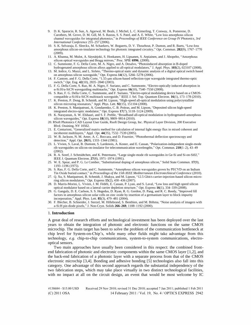
Figure 1 illustrates the device considered in this study. It consists of an optical phase modulator integrated within a p-i-n rib waveguide made of a 2-μm-thick a-Si:H undoped core region between a p-doped a-SiC:H bottom cladding (2-μm-thick) and an n-doped a-SiC:H top cladding (100-nm-thick). A 200-nm-thick transparent conductive oxide (TCO) made of sputtered Al-doped ZnO (ZnO/Al) is present on the waveguide top. The device geometry has been optimised in order to achieve birefringence free propagation [23] and acceptable coupling losses with a standard single-mode fiber with cleaved termination. For this reason, the width of the rib (W) and the height of the waveguide (H) are very large (10 μm and 4.1 μm respectively), and therefore, in order to ensure single mode operation [24], the height of the
#138684 - $15.00 USD Received 29 Nov 2010; revised 31 Dec 2010; accepted 7 Jan 2011; published 1 Feb 2011(C) 2011 OSA 14 February 2011 / Vol. 19, No. 4 / OPTICS EXPRESS 2943
rib is only 400 nm. This choice was made by practical reasons, as it allows relatively low optical losses and easy optical coupling.
The p-type Si substrate serves both as the mechanical support and as the electrical contact for the p-type a-SiC:H layer.
Fig. 1. Schematic cross section of the p-i-n rib-waveguide (a) and material refractive index profile at x = 0 (b). The cross section (a) illustrates the birefringence-free waveguide designed for testing the electro-optical modulation in the a-SiC:H/a-Si:H/a-SiC:H p-i-n structure. From top to bottom we find in sequence a 200 nm-thick ZnO/Al layer, a 100-nm thick a-SiC:H (n-doped) upper cladding, a 2000 nm-thick a-Si:H (undoped) core, and a 2000 nm-thick a-SiC:H (p-doped) bottom cladding. The substrate is a heavily p-doped silicon wafer (300 µm). The refractive index depth profile (b) is based on data measured on separate material samples deposited on Corning glass.
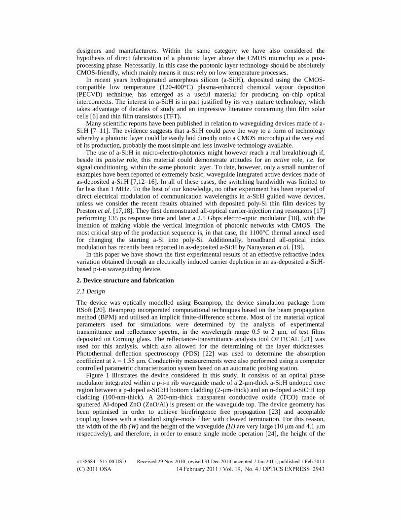
Figure 2 shows the simulated fundamental TE0 and TM0 modes of the structure, including the TCO layer (αZnO/Al = 3.5 dB/cm), respectively characterised by propagation losses of 3.7 dB/cm and 4.5 dB/cm at λ = 1.55μm. These attenuations were confirmed by the experimental results.
Fig. 2. TE (a) and TM (b) simulated fundamental optical mode-field profiles. Parametric beam propagation method (BPM) simulations allowed to design the single-mode, birefringence-free, device shown. The calculated effective refractive indexes neff for the fundamental TE (a) and TM (b) modes are in fact coincident, and at the same time the higher order modes are all vanishing modes.
It is worth noting, in the same figures, the identical values of the real refractive index for the two polarization conditions. Beam propagation method (BPM) numerical calculations of the first-order higher modes TE01 and TM01 show that there is negligible optical field in the waveguide core for these modes and the highest values of the field are localised in the slabs, far from the rib. Thus the TE01 and TM01 are vanishing modes, while the fundamental TE and TM modes are the only ones confined.
#138684 - $15.00 USD Received 29 Nov 2010; revised 31 Dec 2010; accepted 7 Jan 2011; published 1 Feb 2011(C) 2011 OSA 14 February 2011 / Vol. 19, No. 4 / OPTICS EXPRESS 2944

It should be noted that the weak horizontal confinement of this particular device would not allow the fabrication of bended structures. According to simulations, a bend radius of 1.5 cm would already induce radiation losses of the order of 30 dB/cm. A re-design of the waveguide would therefore be necessary for a better confinement of the propagating radiation.
2.2 Fabrication
After a surface cleaning treatment, using H2SO4 + H2O2 and HF solutions, the p-doped c-Si substrate (ρ = 0.001 Ω∙cm) was loaded into the four-chamber PECVD system. First, the a-SiC:H cladding layer was deposited from the plasma-assisted decomposition of SiH4, CH4, B2H6 and H2 at an RF power PRF = 4 W, a frequency of f = 13.56 MHz, and a substrate temperature of T = 120°C. After moving the sample into another deposition chamber, the undoped a-Si:H layer was deposited, at the same temperature, in SiH4 and H2 atmosphere at a VHF (f = 100 MHz) power of PVHF = 50 W. It should be noted that the density of states within the energy gap normally induce a n-type behaviour in undoped a-Si:H films [25]. The deposition of the n-type a-SiC:H layer from a gaseous mixture of SiH4, CH4 and PH3 took place in a third chamber. The deposition times were adjusted to obtain the desired film thicknesses.
The 200-nm-thick TCO layer was deposited by magnetron co-sputtering of ZnO and Al targets, at 25°C substrate temperature. This material shows a good trade-off between optical
(n = 1.87, k = 105
at λ = 1550 nm) and electrical (σ = 6.4·103
S/cm) properties with respect, for example, to Indium Tin Oxide (ITO) or doped polysilicon, which are characterised by a much higher infrared optical absorption [26]. Some samples were covered by a thin metal layer (100 nm of Ag) for the formation of an ohmic contact. The rib definition involved photolithography and reactive ion etching (RIE). A scanning electron microphotograph is reported in Fig. 3, with a cross section of the rib also shown in the inset.
Fig. 3. Scanning electron microphotograph of the realized rib waveguide. From top to bottom we find in sequence a 200 nm-thick ZnO/Al layer, a 100-nm thick a-SiC:H (n-doped) upper cladding, a 2000 nm-thick a-Si:H (undoped) core, and a 2000 nm-thick a-SiC:H (p-doped) bottom cladding. The rib cross section is shown in the inset.
The fundamental process parameters are listed in Table 1 together with the measured material characteristics at λ = l.55 μm. It is worth noting that the maximum temperature during the process is as low as 170°C, which certainly makes it fully compatible with every CMOS process previously performed on the same substrate.
#138684 - $15.00 USD Received 29 Nov 2010; revised 31 Dec 2010; accepted 7 Jan 2011; published 1 Feb 2011(C) 2011 OSA 14 February 2011 / Vol. 19, No. 4 / OPTICS EXPRESS 2945

Table 1. PECVD process parameters and main optical and electrical parameters. RF frequency and power during deposition, substrate temperature, deposition rate and final layer thickness. Process gas flows are measured in standard cubic centimetres per minute
(sccm). Refractive index, n, and extinction coefficient, κ, are measured at 1550 nm. (*0.5% diluted in H2)
Material f
[MHz] Power [W]
Pressure [hPa]
T [°C]
Deposition Rate [Å/s]
Layer Thickness
[m]
Process Gas [sccm]
n k
[S/cm]
a-SiC:H (p)
13.56 4 0.8 120 2.74 2
SiH4 CH4 B2H6* H2
2.990.02 5.3·10-3 2.3·10-6 6 6 10 20
a-Si:H (i) 100 50 0.3 120 23.5 2 SiH4 H2
3.200.02 2.4·10-6 10-10 20 20
a-SiC:H (n) 13.56 4 0.9 170 2.85 0.1 SiH4 CH4 PH3
2.890.02 2.8·10-3 1.9·10-8 25 35 3
3. Experimental results and discussion
The forward and reverse J-V characteristics of the p-i-n device are shown in Figs. 4a and 4b. It clearly shows a rectifying behaviour, but the very high ideality factor in the forward bias (n >10) suggests that the current is largely controlled by recombination at low currents, and subsequently by a high series resistance. We could in fact apply forward biases as high as 45 V, measuring a current density of 1.8 A/cm
2. At this regime the current density is certainly
limited by the specific series resistance, which we estimated to be 15 Ω∙cm2. In reverse bias
the current density is lower than 10 nA/cm2 up to 50 V. Afterwards, a soft breakdown effect
is present, determining the reverse current density to rise to 55 nA/cm2 at 80 V. In all
samples a destructive reverse breakdown occurs between 90 and 110 V. The small signal specific capacitance device at zero bias is 1.75 nF/cm
2, measured at 1 MHz, a frequency at
which most of the carriers trapped in gap states of a-Si:H are frozen. The present device is quite different from the one we previously used in [15,16], where
multiple insulator-semiconductor couples where exploited for inducing several thin accumulation layers well distributed across the active waveguide section, which has however shown long response times.
The application of a forward bias might also be in principle a valid mean for inducing a carrier concentration variation throughout the undoped region [16]. The long drift region of the present structure, coinciding with the neutral portion of the a-Si:H layer, prevents however the reaching of a suitable injection level throughout it.
In our experiments, a 30 mW tunable laser-diode, with a central wavelength λ of 1.55 μm, was the source of the probe radiation. The light beam was coupled into the p-i-n device via a standard single mode fibre. The transmitted light was collected at the chip output by a single-mode fibre and detected by an amplified InGaAs photodiode. Great care was taken to prevent stray light passing above the sample.
#138684 - $15.00 USD Received 29 Nov 2010; revised 31 Dec 2010; accepted 7 Jan 2011; published 1 Feb 2011(C) 2011 OSA 14 February 2011 / Vol. 19, No. 4 / OPTICS EXPRESS 2946

Fig. 4. Forward (a) and reverse (b) bias J-V characteristics of the p-i-n device. The ideality factor n of the diode in forward bias is higher than 10, showing that the current is dominated by
carrier recombination, at least up to 2 × 10³ A/cm2 current density. At higher current regimes the characteristic bends as an effect of the high series resistance due to the neutral region of the undoped layer and to the relatively low doped anode and cathode regions.
Separate samples were obtained by cleavage with lengths in the range from 750 to 1500 μm. Those showing good optical quality of the facets demonstrated the clear behaviour of Fabry-Perot (FP) cavities. For a 750 μm long cavity (Fig. 5) we measured a free spectral range (FSR) of 0.493 ± 0.003 nm, allowing the calculation of group index ng of 3.34 ± 0.02, a value also confirmed in other samples. For the same sample, the observed extinction ratio (ER) Imax/Imin was 1.65 ± 0.04, with Imax and Imin the maximum and minimum transmitted signals respectively. From this value, the waveguide losses were calculated using Eq. (1),
max min
max min
/ 11 1ln
/ 1
I I
L R I I
(1)
deriving from Airy’s well-known formula, where L is the cavity length and R = (na-Si-no)2/(na-Si
+ no)2 is the facet reflectance, with no the refractive index of air and na-Si taken from Table 1.
In particular we obtained α = 10.5 ± 0.3 cm1
, a rather high loss coefficient that is justified by the presence of the metal film on the waveguide top. The overall losses of the device are above 20 dB, with the main contribution due to coupling and absorption losses. It is worth noting, in connection, that measurements performed on waveguides without metal contact provided losses of 5 ± 1 dB/cm, in agreement with simulations. In an improved design the metal contact should therefore be placed not above, but aside of the waveguide.
The phase modulation measurements relied on the shift of the Fabry-Perot fringes when a reverse bias is applied to the p-i-n diode by means of a shielded micro-probe. In Fig. 5 we report the transmission spectra of the 750 µm cavity at zero bias and at 70 V. The observed red-shift of the fringes is consistent with the assumption that the carrier depletion induced in the waveguide core determines an increase of the effective refractive index neff.
In the same figure (see inset), the peak wavelength variation Δλmax is 0.018 nm, from which the induced Δneff of the guided mode was estimated as follows:
)()(
geff nn
(2)
#138684 - $15.00 USD Received 29 Nov 2010; revised 31 Dec 2010; accepted 7 Jan 2011; published 1 Feb 2011(C) 2011 OSA 14 February 2011 / Vol. 19, No. 4 / OPTICS EXPRESS 2947

Fig. 5. Experimental transmission spectra of a 750 μm-long unbiased and reverse biased (70 V)
p-i-n device. The calculated index variation is 4.05 × 10⁵.
where ng is the group index determined according to Eq. (3):
FSRL
ng
2
2
(3)
where FSR is the experimental wavelength distance between two successive resonance peaks, and L is the device length. The results obtained on several 750 and 1000-μm-long samples at five distinct biases are summarized in Fig. 6.
A comparison can be made between these results and those obtained in Ref [19]. by
photogeneration. With a photoinduced excess free carrier concentration of ~2 × 10¹⁸
cm3
[19]
Fig. 6. Experimental effective index variation versus p-i-n reverse bias voltage ranging from 0 to 90V.
#138684 - $15.00 USD Received 29 Nov 2010; revised 31 Dec 2010; accepted 7 Jan 2011; published 1 Feb 2011(C) 2011 OSA 14 February 2011 / Vol. 19, No. 4 / OPTICS EXPRESS 2948
and the effective masses given therein, the Δneff estimated by the Drude model [15] is in that
case ~8 × 10⁴
. The weaker effect on the refractive index in our device is justified by the intrinsic differences between the two approaches, as in our case the maximum free carrier variation has a fundamental limit in the equilibrium free carrier concentration, governed in turn by the deposition parameters.
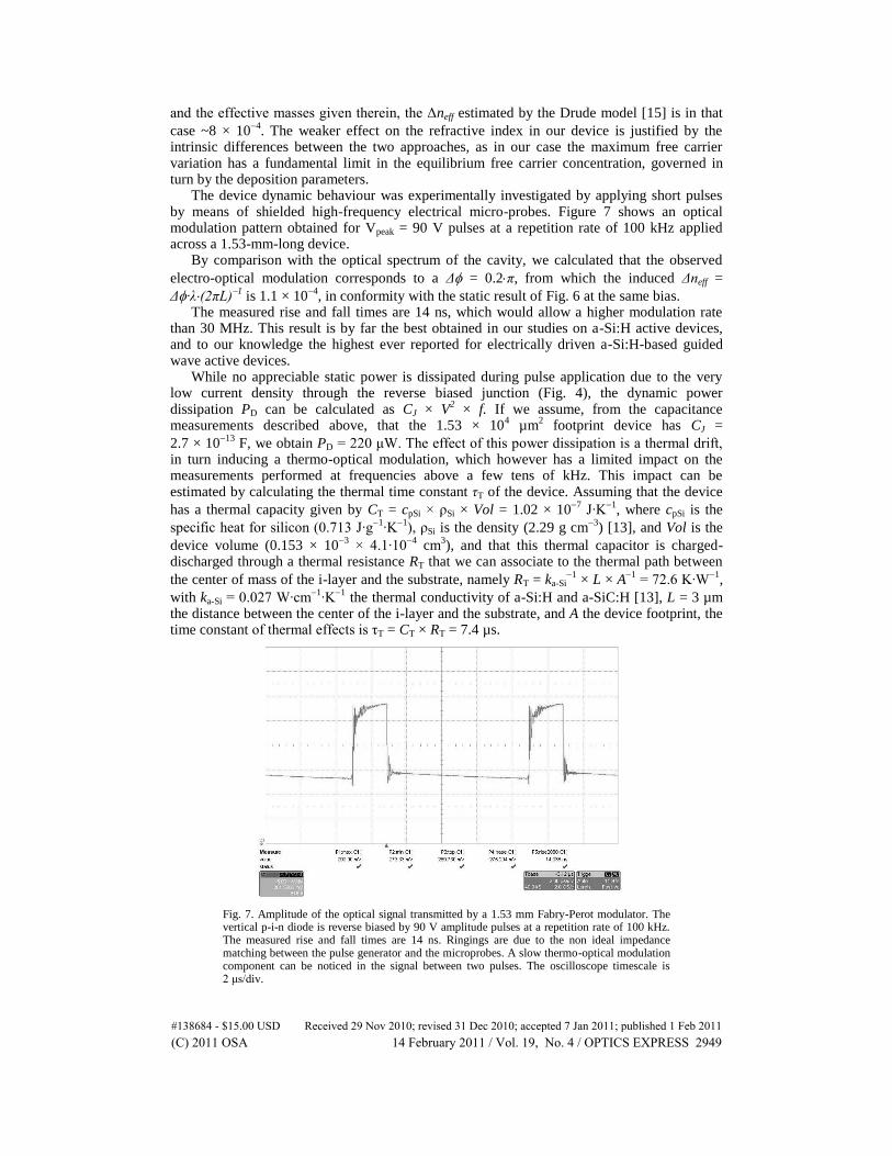
The device dynamic behaviour was experimentally investigated by applying short pulses by means of shielded high-frequency electrical micro-probes. Figure 7 shows an optical modulation pattern obtained for Vpeak = 90 V pulses at a repetition rate of 100 kHz applied across a 1.53-mm-long device.
By comparison with the optical spectrum of the cavity, we calculated that the observed
electro-optical modulation corresponds to a Δ = 0.2π, from which the induced Δneff =
Δ·λ(2πL)1 is 1.1 × 10
4, in conformity with the static result of Fig. 6 at the same bias.
The measured rise and fall times are 14 ns, which would allow a higher modulation rate than 30 MHz. This result is by far the best obtained in our studies on a-Si:H active devices, and to our knowledge the highest ever reported for electrically driven a-Si:H-based guided wave active devices.
While no appreciable static power is dissipated during pulse application due to the very low current density through the reverse biased junction (Fig. 4), the dynamic power dissipation PD can be calculated as CJ × V
2 × f. If we assume, from the capacitance
measurements described above, that the 1.53 × 104 µm
2 footprint device has CJ =
2.7 × 10¹³
F, we obtain PD = 220 μW. The effect of this power dissipation is a thermal drift, in turn inducing a thermo-optical modulation, which however has a limited impact on the measurements performed at frequencies above a few tens of kHz. This impact can be estimated by calculating the thermal time constant τT of the device. Assuming that the device
has a thermal capacity given by CT = cpSi × ρSi × Vol = 1.02 × 10⁷
J∙K1
, where cpSi is the
specific heat for silicon (0.713 J∙g1
∙K1
), ρSi is the density (2.29 g cm3
) [13], and Vol is the
device volume (0.153 × 103
× 4.1∙104
cm3), and that this thermal capacitor is charged-
discharged through a thermal resistance RT that we can associate to the thermal path between
the center of mass of the i-layer and the substrate, namely RT = ka-Si1
× L × A1
= 72.6 K∙W1
,
with ka-Si = 0.027 W∙cm1
∙K1
the thermal conductivity of a-Si:H and a-SiC:H [13], L = 3 µm the distance between the center of the i-layer and the substrate, and A the device footprint, the time constant of thermal effects is τT = CT × RT = 7.4 µs.
Fig. 7. Amplitude of the optical signal transmitted by a 1.53 mm Fabry-Perot modulator. The vertical p-i-n diode is reverse biased by 90 V amplitude pulses at a repetition rate of 100 kHz. The measured rise and fall times are 14 ns. Ringings are due to the non ideal impedance matching between the pulse generator and the microprobes. A slow thermo-optical modulation component can be noticed in the signal between two pulses. The oscilloscope timescale is 2 μs/div.
#138684 - $15.00 USD Received 29 Nov 2010; revised 31 Dec 2010; accepted 7 Jan 2011; published 1 Feb 2011(C) 2011 OSA 14 February 2011 / Vol. 19, No. 4 / OPTICS EXPRESS 2949

This approximate value, which is notably in agreement with previous experimental outcomes [7] on similar devices, demonstrates that the observed 10-ns-scale rise and fall times of Fig. 7 are not compatible with a thermo-optic modulation. In the same figure we note however the presence of a slow drift of the signal between two pulses that can be put in relation to a thermal drift.
The turn-on/turn-off transients are indeed limited by the high series resistance of the device estimated above (15 Ω∙cm
2). From this, in fact, a characteristic time constant derives at
Rs × CJ ~27 ns. To evaluate the phase modulation efficiency, a figure of merit is usually adopted, defined
as the product VπLπ, where Vπ and Lπ are respectively the bias voltage and the waveguide length required to obtain a π phase shift of the guided wave. With the measured Δneff at 90 V,
we get VπLπ = 63 V·cm. This rather poor figure of merit, at least one order of magnitude higher than that demonstrated on crystalline silicon [27,28], is certainly penalized by the waveguide core, i.e. the i-layer, thickness (ta-Si = 2 µm). The impact of the i-layer thickness on Vπ can in fact be roughly estimated by recalling that in this p-i-n structure the full-depletion bias VFD can be calculated from:
Sia
i
FDSi tNq
VW
21
max
2 (4)
with Wmax the maximum allowed depletion width, Ni the i-layer doping and εSi = ε0·εr the permittivity of silicon with εr = 11.8. This relationship, graphically shown in Fig. 8 in the
doping range from 1011
to 1014
cm3
, indicates that, for a given doping, the full depletion is obtained for voltages that scale with a square low with the thickness.
Fig. 8. Calculated full depletion bias (VFD) of a p-i-n waveguide as a function the i-layer doping. The three curves refer to different i-layer thicknesses.
If we now assume that, according to the Drude model [15], by driving the waveguide in full depletion, its effective refractive index variation, Δneff, is proportional to the starting free carrier concentration Ni, we find that for a given Δneff the necessary full-depletion bias VFD is scaled with t
2a-Si.
Additional considerations can be made in the prospect of a practical optimized device. For example, although the time constant Rs × CJ is to a first order not dependent on the device footprint, because the electrode area has opposite effects on Rs and CJ, series resistances lower
than 1 Ωcm2 are generally achieved in a-Si:H based solar cells [29,30]. We can therefore
#138684 - $15.00 USD Received 29 Nov 2010; revised 31 Dec 2010; accepted 7 Jan 2011; published 1 Feb 2011(C) 2011 OSA 14 February 2011 / Vol. 19, No. 4 / OPTICS EXPRESS 2950

expect time constants lower than 2 ns to be possible in devices with the same geometry and better I-V characteristics. We add that a reduction of the junction capacitance can be obtained, for a given contact footprint, with fully-etched channel waveguides, where the lateral effect of the electric field, i.e. the effective device volume, is certainly lower.
The dynamic power is a major concern at high frequency modulation regimes. Assuming
CJ = εSi × A × (ta-Si)1
, with A the device area, from Eq. (4) we obtain that the energy-per-bit Epb can be estimated from:
Sia
Si
ipb t
NqAE
4
2
(5)
which, for a 1-μm-wide, 1-mm-long, 500-nm-thick, channel waveguide, allows to calculate an
energy dissipation of ~3 pJ/bit for Ni = 1012
cm3
.
7. Conclusion
We have shown that effective electro-optical modulation at λ = 1.55 μm can be produced by reverse biasing a p-i-n waveguiding structure based on the CMOS-compatible technology of a-Si:H.
The device was fabricated on a silicon substrate by PECVD at a maximum process temperature of 170 °C. The phase modulation was studied in Fabry-Perot resonators, in which
the voltage-length product for inducing a phase variation Δ = π in a travelling wave was
determined to be Vπ∙Lπ = 63 Vcm. The corresponding refractive index variation due to electric-field induced free carrier depletion effect in the p-i-n waveguiding device was
calculated to be 1.1 × 10⁴
. Characteristic switch-on and switch-off times of 14 ns were measured allowing a higher
modulation rate than 30 MHz, the highest value ever reported for waveguide-integrated electrically driven a-Si:H-based optical devices.
Beside photonics on CMOS, the limited temperature involved in its fabrication could pave the way to the deployment of active photonics in applications where the process temperature is an important issue, like on plastics and glasses.
Acknowledgements
The authors wish to thank P. Viktorovitch (Institut des Nanotechnologies de Lyon-INL, France) and L. Vivien (Institut d’Electronique Fondamentale, CNRS-University of Paris Sud, France) for stimulating discussions. The authors are also grateful to Dr. M. Gioffrè and the technology staff of IMM-CNR for clean room processes. The research leading to these results has received funding from the European Community’s Seventh Framework Programme (FP7/2007-2013) under grant agreement n° 224312 HELIOS.
#138684 - $15.00 USD Received 29 Nov 2010; revised 31 Dec 2010; accepted 7 Jan 2011; published 1 Feb 2011(C) 2011 OSA 14 February 2011 / Vol. 19, No. 4 / OPTICS EXPRESS 2951


![Prof. D. R. Wilton Notes 19 Waveguiding Structures Waveguiding Structures ECE 3317 [Chapter 5]](https://static.fdocuments.us/doc/165x107/56649e975503460f94b9aba9/prof-d-r-wilton-notes-19-waveguiding-structures-waveguiding-structures-ece.jpg)


![of fish oil, partially hydrogenated soybean oil, and ... · Effects of partially hydrogenated fish oil, partially hydrogenated soybean oil, and butter on serum lipoproteins and Lp[a]](https://static.fdocuments.us/doc/165x107/5cdad3f488c993a0658b8335/of-fish-oil-partially-hydrogenated-soybean-oil-and-effects-of-partially.jpg)