Electrically bistable digital memory behaviors of thin films of
32
Accepted Manuscript Electrically bistable digital memory behaviors of thin films of polyimides based on conjugated Bis(triphenylamine) derivatives Kyungtae Kim, Hung-Ju Yen, Yong-Gi Ko, Cha-Wen Chang, Wonsang Kwon, Guey- Sheng Liou, Moonhor Ree PII: S0032-3861(12)00606-4 DOI: 10.1016/j.polymer.2012.07.025 Reference: JPOL 15548 To appear in: Polymer Received Date: 12 April 2012 Revised Date: 9 July 2012 Accepted Date: 14 July 2012 Please cite this article as: Kim K, Yen H-J, Ko Y-G, Chang C-W, Kwon W, Liou G-S, Ree M, Electrically bistable digital memory behaviors of thin films of polyimides based on conjugated Bis(triphenylamine) derivatives, Polymer (2012), doi: 10.1016/j.polymer.2012.07.025. This is a PDF file of an unedited manuscript that has been accepted for publication. As a service to our customers we are providing this early version of the manuscript. The manuscript will undergo copyediting, typesetting, and review of the resulting proof before it is published in its final form. Please note that during the production process errors may be discovered which could affect the content, and all legal disclaimers that apply to the journal pertain.
Transcript of Electrically bistable digital memory behaviors of thin films of
Accepted Manuscript
Electrically bistable digital memory behaviors of thin films of polyimides based onconjugated Bis(triphenylamine) derivatives
Kyungtae Kim, Hung-Ju Yen, Yong-Gi Ko, Cha-Wen Chang, Wonsang Kwon, Guey-Sheng Liou, Moonhor Ree
PII: S0032-3861(12)00606-4
DOI: 10.1016/j.polymer.2012.07.025
Reference: JPOL 15548
To appear in: Polymer
Received Date: 12 April 2012
Revised Date: 9 July 2012
Accepted Date: 14 July 2012
Please cite this article as: Kim K, Yen H-J, Ko Y-G, Chang C-W, Kwon W, Liou G-S, Ree M, Electricallybistable digital memory behaviors of thin films of polyimides based on conjugated Bis(triphenylamine)derivatives, Polymer (2012), doi: 10.1016/j.polymer.2012.07.025.
This is a PDF file of an unedited manuscript that has been accepted for publication. As a service toour customers we are providing this early version of the manuscript. The manuscript will undergocopyediting, typesetting, and review of the resulting proof before it is published in its final form. Pleasenote that during the production process errors may be discovered which could affect the content, and alllegal disclaimers that apply to the journal pertain.

MANUSCRIP
T
ACCEPTED
ACCEPTED MANUSCRIPT
MANUSCRIP
T
ACCEPTED
ACCEPTED MANUSCRIPT
Ms. No: POLYMER-12-718 1st Revision on May 15, 2012 2nd Revision on July 9, 2012
(The revised parts are highlighted with Yellow color.)
Electrically Bistable Digital Memory Behaviors of Thin Films of
Polyimides Based on Conjugated Bis(triphenylamine) Derivatives
Kyungtae Kim,1,† Hung-Ju Yen,2,† Yong-Gi Ko,1 Cha-Wen Chang,2 Wonsang Kwon,1 Guey-
Sheng Liou,2,* and Moonhor Ree1,*
1Department of Chemistry, Division of Advanced Materials Science, Center for Electro-Photo
Behaviors in Advanced Molecular Systems, Pohang Accelerator Laboratory, Polymer Research
Institute, and BK School of Molecular Science, Pohang University of Science & Technology,
Pohang 790-784, Republic of Korea
2Institute of Polymer Science and Engineering, National Taiwan University, Taipei 10617,
Taiwan
___________________________________________ *To whom correspondence should be addressed. E-mail: [email protected] (M.R.), [email protected] (G.-S.L.) Tel: +82-54-279-2120 (M.R.), +886-2-3336-5315 (G.-S.L.); Fax: +82-54-279-3399 (M.R.), +886-2-3336-5237 (G.-S.L.)
†K. Kim and H.-J. Yen contributed equally to this work.

MANUSCRIP
T
ACCEPTED
ACCEPTED MANUSCRIPT
2
Abstract
Three functional polyimides (PIs) bearing conjugated bis(triphenylamine) (2TPA)
derivatives with electron-donating and accepting groups were synthesized with reasonably high
molecular weights. The PIs exhibited high thermal and dimensional stabilities and furthermore
produced high-quality nanoscale thin films via conventional solution coating process. All of the
PIs in the films were found to be amorphous, but they were oriented somewhat preferentially in
the film plane, rather than randomly. Their film densities and interchain distances were measured,
and the optical and electrochemical properties were determined. All of the PIs in the devices with
aluminum top and bottom electrodes initially revealed a high resistance (OFF-state). However,
under positive and negative voltage sweeps, the PIs demonstrated volatile or nonvolatile digital
memory behavior, depending on the substituents of the 2TPA unit. The 2TPA-based PI, as well as
the PI bearing 2TPA with electron-donating methoxy substituents showed unipolar write-once-
read-many-times (WORM) memory behavior, whereas the 2TPA-based PI containing electron-
accepting cyano groups exhibited unipolar dynamic random access memory (DRAM) behavior.
All of the PI films revealed excellent retention abilities in both the OFF- and ON-state, even
under ambient air conditions. Moreover, they all revealed high ON/OFF current ratios (106-1010).
All of the memory behaviors were found to be governed by a mechanism involving trap-limited
space-charge limited conduction and local filament formation. Such memory behaviors were
further investigated in detail with taking into consideration the PI components’ chemical nature
and molecular orbital levels, possible trapping sites, substituents’ effect, and the metal electrodes’
work function. Overall, this study demonstrated that the thermally, dimensionally stable PIs are
highly suitable for the low-cost mass production of high performance, polarity-free digital
memory devices that can be operated with very low power consumption. Moreover, the memory
mode can be tuned by changing the substituent in the 2TPA unit.
(Keywords: High temperature aromatic polyimide, bis(triphenylamine) derivatives, nonvolatile
memory, volatile memory, electrical switching mechanism, high retention stability, low power
consumption)

MANUSCRIP
T
ACCEPTED
ACCEPTED MANUSCRIPT
3
1. Introduction
In general, polymers can be easily processable in various ways, including conventional
solution coating and melt molding, and their structures and properties can be tailored through
chemical synthesis. Furthermore, polymers can be easily incorporated into a highly dense
multilayer structure of advanced memory devices, which are currently demanded for the storage
of multimedia data, such as videos [1-5].
In particular, aromatic polyimides (PIs) are known to possess excellent thermal stability,
dimensional stability, and mechanical properties [6-10]. Due to these advantageous properties,
much effort has recently been made to develop high performance PI materials for advanced
memory devices [11-18]. As a result, several PIs were reported for the fabrication of memory
devices [11-18]. They revealed various memory behaviors (i.e., switchable, permanent and
volatile memories) with unipolarity or bipolarity, depending on the chemical structure as well as
the film thickness. Poly(4,4’-aminotriphenylene hexafluoroisopropylidenediphthalimide) (6F-
TPA PI) was reported to exhibit dynamic random access memory (DRAM)) behavior with
polarity [11]. Compared to 6F-TPA PI, poly(4,4’-amino(4-hydroxyphenyl)diphenylene
hexafluoroisopropylidenediphthalimide) additionally possessed only one hydroxyl group per TPA
unit, but interestingly revealed unipolar write-once-read-many-times (WORM) memory behavior
[12], which was quite different from the bipolar DRAM behavior observed for 6F-TPA PI.
Furthermore, poly(N-(N’ ,N’-diphenyl-N’ -1,4-phenyl)-N,N-4,4’-diphenylene hexafluoroiso-
propylidenediphthalimide) (6F-2TPA PI) revealed volatile DRAM behavior with polarity and
nonvolatile WORM memory characteristics with and without polarity depending on the thickness
[13]; namely, the 100 nm thick films showed DRAM behavior while the films with a thickness of
>15 to <100 nm exhibited WORM behavior. Poly(3,3’-di(4-(diphenylamino)benzylidenyl-
iminoethoxy)-4,4’-biphenylene hexafluoroisopropylidenediphthal-imide) demonstrated unipolar

MANUSCRIP
T
ACCEPTED
ACCEPTED MANUSCRIPT
4
and bipolar nonvolatile switching behaviors [14]. Poly(3,3’-bis(diphenylcarbamyloxy)-4,4’-
biphenylene hexafluoroisopropylidenediphthalimide) was found to exhibit rewritable nonvolatile
memory characteristics [15]. On the other hand, poly(3,3’-bis(N-ethylenyloxycarbazole)-4,4’-
biphenylene hexafluoroisopropylidenediphthalimide), a polyimide containing carbzole moieties,
demonstrated rewritable unipolar nonvolatile memory behavior [16]. In contrast, other aromatic
polyimides containing carbazole moieties (which were synthesized from 3,3’-bis[9-
carbazole(ethyloxy)biphenyl]-4,4’-diamine) exhibited unipolar WORM memory behaviors,
regardless of the dianhydride units in the polymer backbone [17]. Poly(3,3’-di(9-
anthracenemethoxy)-4,4’-biphenylene hexafluoroisopropyl-idenediphthalimide), a polyimide
containing anthracene moieties, revealed rewritable unipolar and bipolar nonvolatile memory
behaviors [18]. Overall, the development of high-performance PIs for memory devices still
remains in its early stages. Furthermore, to facilitate the development of high performance
memory PIs, it is essential to understand the relationship between their electrical memory
behavior and their chemical structure.
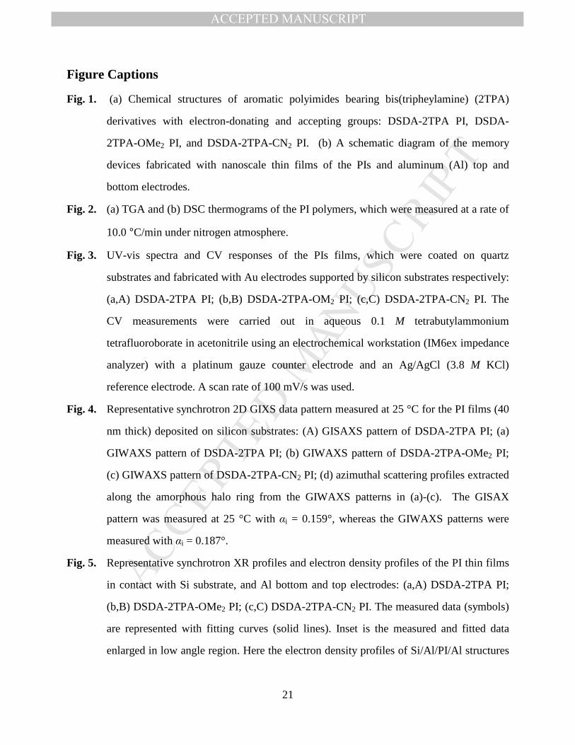
In this study, we synthesized three aromatic PIs bearing bis(tripheylamine) (2TPA)
derivatives with electron-accepting and donating groups, and investigated their electrical memory
behaviors: poly(N,N-bis(4-aminophenyl)-N’,N ’-diphenyl-1,4-phenylene 3,3’,4,4’-
diphenylsulfonyltetracarboximide) (DSDA-2TPA PI), poly(N,N-bis(4-aminophenyl)-N’,N ’-di(4-
methoxyphenyl)-1,4-phenylene 3,3’,4,4’-diphenylsulfonyltetracarboximide) (DSDA-2TPA-OMe2
PI), and poly(N,N-bis(4-aminophenyl)-N’,N ’-di(4-cyanophenyl)-1,4-phenylene 3,3’,4,4’-
diphenylsulfonyltetracarboximide) (DSDA-2TPA-CN2 PI) (Fig. 1a). The PIs exhibited high
thermal and dimensional stability, and produced high quality nanoscale thin films via
conventional solution coating and drying process. These PIs were found to reveal write-once-
read-many-times (WORM) memory and dynamic random access memory (DRAM) behaviors

MANUSCRIP
T
ACCEPTED
ACCEPTED MANUSCRIPT
5
without polarity, depending on the 2TPA derivatives. The observed memory characteristics were
understood with taking into consideration the chemical nature including substituents,
morphological structure and interface, and optical and electrochemical properties, as well as the
work functions of metal electrodes. In addition, their switching mechanism was investigated.
2. Experimental
DSPA-2TPA PI was synthesized in N-methyl-2-pyrrolidinone (NMP) from 3,3’,4,4’-
diphenylsulfonyltetracarboxylic dianhydride (DSDA) and N,N-bis(4-aminophenyl)-N’,N ’-
diphenyl-1,4-phenylene diamine (2TPA) as described in the literature [19]. In similar synthetic
manner, DSDA-2TPA-OMe2 PI and DSDA-2TPA-CN2 PI were prepared from the
polymerizations of DSDA with N,N-bis(4-aminophenyl)-N’,N ’-di(4-methoxyphenyl)-1,4-
phenylene diamine (2TPA-OMe2) and N,N-bis(4-aminophenyl)-N’,N ’-di(4-cyanophenyl)-1,4-
phenylene diamine (2TPA-CN2) respectively.
For the obtained PIs, inherent viscosities were determined with a concentration of 0.5 g/dL
in NMP at 30 °C using a Tamson TV-2000 viscometer. Furthermore, for some selected PIs,
molecular weights were measured at 70 °C using a gel permeation chromatography (GPC) system
(Lab Alliance RI2000 Instruments) connected with a refractive index detector (Schambeck SFD
Gmbh). The GPC system was calibrated with polystyrene standards; N,N-dimethylformamide
(DMF) was used with a flow rate of 1 mL/min as the eluent. Thermal properties were measured in
nitrogen atmosphere using a thermogravimetric analyzer (model TG/DTA-6300, Seiko) and a
differential scanning calorimeter (model DSC 220CU, Seiko); dry nitrogen gas was purged at a
flow rate of 100 cc/min and a ramping rate of 10.0 °C/min were employed.

MANUSCRIP
T
ACCEPTED
ACCEPTED MANUSCRIPT
6
Aluminum (Al) bottom electrodes with a thickness of 300 nm were prepared onto
precleaned silicon (Si) substrates by electron-beam deposition. Homogenous solutions of the
three PIs were prepared by dissolving the polymers (1 wt%) in cyclopentanone. The resulting
solutions were filtered through PTFE-membrane microfilters with a pore size of 1.0 µm. The
polymer solutions were spin-coated onto the electrodes and Si substrates at 2000 rpm for 60 s.
The films were then baked at 80 °C for 24 h in vacuum. The thicknesses of the PI films were
determined using a spectroscopic ellipsometer (model M2000, Woollam). Al top electrodes were
thermally evaporated onto the polymer films at a pressure of ~10-6 torr through a shadow mask.
The top electrodes had a thickness of 300 nm and their area varied from 2.0 mm × 2.0 mm to 0.5
mm × 0.5 mm.
For X-ray reflectivity (XR) experiments, we prepared three kinds of samples for each
polymer: (i) 30 nm thick PI films on Si substrates with native oxide layer; (ii) 30 nm thick PI
films on the 10 nm thick Al electrodes which were deposited on Si substrates by electron-beam
sputtering; (iii) thermally evaporated 10 nm thick Al electrodes on the 30 nm thick PI films
coated onto Si substrates. Synchrotron XR measurements were performed at the 3C2 and 8C1
POSCO beamlines of the Pohang Accelerator Laboratory (PAL) [20]. A Si(111) double-crystal
monochromator was used to select a wavelength λ of 0.1541 nm within an energy resolution of
∆λ / λ = 5×10⁻⁴, and a Saggital bender for the second crystal was used to focus the X-ray beam in
the horizontal direction. The primary beam was defined by four slits before the sample, and
another two slits were used as receiving slits after the sample. The beam was collimated at the
sample position to 2 mm (horizontal) by 0.1 mm (vertical). The measured reflected intensity was
normalized to the intensity of the primary beam, which was monitored with an ionization
chamber. Specular reflection was measured in θ–2θ scanning mode. The reflectivity R, i.e. the
MANUSCRIP
T
ACCEPTED
ACCEPTED MANUSCRIPT
7
ratio of the reflected beam intensity to the primary beam intensity, was measured down to just
above 10-8. To obtain accurate determinations of the critical angles of the silicon substrate and of
the thin film, 2θ was scanned at small increments of 0.01° at angles smaller than 1.0°. At higher
angles the step width was increased to 0.02–0.1°. The obtained data were undergone data binning,
geometrical correction, and background subtraction procedure described in literature [20,21].
Grazing-incidence X-ray scattering (GIXS) measurement was performed at the PAL 3C
beamline [22,23]. Measurements were performed at a sample-to-detector distance (SDD) of 125
mm for grazing incidence wide-angle X-ray scattering (GIWAXS) and 2220 mm for grazing
incidence small-angle X-ray scattering (GISAXS). Scattering data were typically collected for 30
s using X-ray radiation source of λ = 0.138 nm with a two-dimensional (2D) charge-coupled
detector (CCD) (Roper Scientific, Trenton, NJ, USA). The incidence angle αi of the X-ray beam
was set at 0.183° for GIWAXS and 0.160° for GISAXS, respectively, which are between the
critical angles of the PI film and the silicon substrate (αc,f and αc,s). Scattering angles were
corrected according to the positions of the X-ray beams reflected from the silicon substrate with
respect to a pre-calibrated silver behenate (TCI, Japan) powder. Aluminum foil pieces were
applied as a semitransparent beam stop because the intensity of the specular reflection from the
substrate was much stronger than the scattering intensity of the polymer films near the critical
angle.
Current−voltage (I–V) characteristics of the device were tested in air ambient condition
using a Keithley 4200 semiconductor analyzer. I–V curves were recorded by performing forward
and reverse voltage scans between −6.0 V and +6.0 V at a scan rate of 500 mV/s. Optical
properties were measured with a Scinco ultraviolet-visible (UV-vis) spectrometer (model S-
3100). Cyclic voltammetry (CV) measurements were carried out in an 0.1 M solution of
tetrabutylammonium tetrafluoroborate in acetonitrile by using an electrochemical workstation
MANUSCRIP
T
ACCEPTED
ACCEPTED MANUSCRIPT
8
(IM6ex impedance analyzer) with a platinum gauze counter electrode and an Ag/AgCl (saturated
KCl) reference electrode, and polymers were coated onto the Au bottom electrode, which was
deposited on a silicon wafer. A scan rate of 100 mV/s was used.
3. Results and Discussion
The inherent viscosity ηinh was measured to be 0.72 dL/g for DSDA-2TPA PI, 0.64 dL/g for
DSDA-2TPA-OMe2 PI, and 0.99 dL/g for DSDA-2TPA-CN2 PI. For some of the PIs, the weight
average molecular weight (wM ) and polydispersity index (PDI) were further determined by GPC
analysis. The wM and PDI were 64000 and 1.40 for DSDA-2TPA PI, and 80000 and 1.47 for
DSDA-2TPA-OMe2 PI. Overall, all of the PIs were synthesized with reasonably high molecular
weights. The onset temperature of degradation (Td) was measured in nitrogen atmosphere to be
397 °C for DSDA-2TPA PI, 368 °C for DSDA-2TPA-OMe2 PI, and 382 °C for DSDA-2TPA-
CN2 PI (Fig. 2a). The onset temperature of glass transition (Tg) was measured to be 295 °C for
DSDA-2TPA PI, 271 °C for DSDA-2TPA-OMe2 PI, and 297 °C for DSDA-2TPA-CN2 PI (Fig.
2b). Overall, the thermal and dimensional stabilities are comparable to those of conventional
aromatic PIs. The thermal property analysis found that the Td of DSDA-2TPA PI was reduced by
the incorporation of methoxy and cyano group. The Tg of DSDA-2TPA PI was slightly increased
by the incorporation cyano group and, however, reduced by the incorporation of methoxy group.
Figs. 3a-c show the UV-vis absorption spectra of the PIs in thin films. From the spectra, the
band gap (which is the difference between the highest occupied molecular orbital (HOMO) level
and the lowest unoccupied molecular orbital (LUMO) level) was determined to be 2.95 eV for
DSDA-2TPA PI, 3.05 eV for DSDA-2TPA-OMe2 PI, and 3.07 eV for DSDA-TPA-CN2 PI. Figs.
3A-C display the CV data of the PIs. The oxidation half-wave potentials (E1/2) vs. Ag/AgCl was

MANUSCRIP
T
ACCEPTED
ACCEPTED MANUSCRIPT
9
measured to be 0.69 V for DSDA-2TPA PI, 0.60 V for DSDA-2TPA-OMe2 PI, and 0.75 V for
DSDA-TPA-CN2 PI. The E1/2 for the external ferrocene/ferrocenium (Fc/Fc+) system was
measured to be 0.57 V vs. Ag/AgCl in acetonitrile. Assuming that the HOMO level for the Fc/Fc+
standard is −4.80 eV with respect to the zero vacuum level, the HOMO level was estimated to be
−4.92 eV for DSDA-2TPA PI, −4.83 eV for DSDA-2TPA-OMe2 PI, and −4.98 eV for DSDA-
2TPA-CN2 PI. From the measured band gap and HOMO level data, the LUMO level was
calculated to be −1.97 eV for DSDA-2TPA PI, −1.78 eV for DSDA-2TPA-OMe2 PI, and −1.91
eV for DSDA-2TPA-CN2 PI. These results indicate that the electron-donating methoxy
substituent increased the HOMO level of the DSDA-2TPA PI, whereas the electron-accepting
cyano substituent reduced the HOMO level. The tendency of the HOMO level is consistent with
previous studies with conjugated polymers [24]. The band gap of DSDA-2TPA PI was somewhat
increased by the methoxy and cyano substituents, leading to higher LUMO levels of the DSDA-
2TPA-OMe2 and DSDA-2TPA-CN2 PIs.
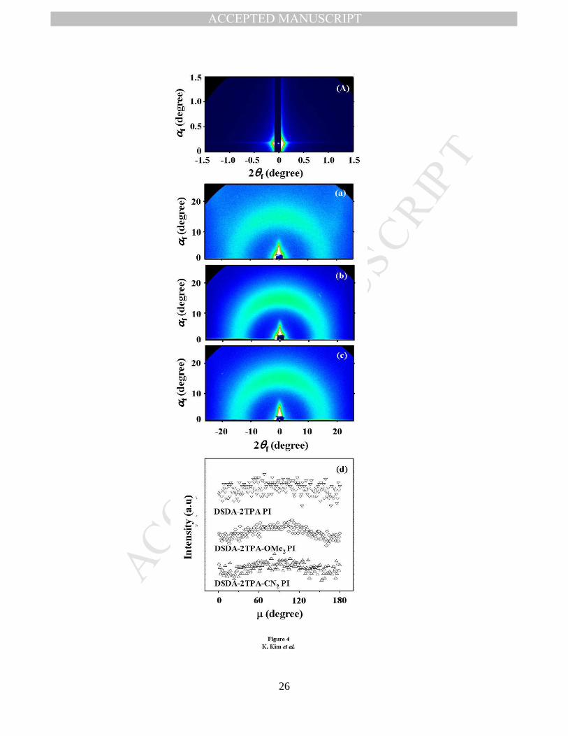
The structures of the PIs in nanoscale thin films were examined by synchrotron GIXS
analysis. The DSDA-2TPA PI film showed featureless 2D GISAXS pattern (Fig. 4A). Similar
GISAXS patterns were observed for the other PIs in films (data not shown). These results indicate
that no discernible nanostructure or microstructures were developed in all the PI films. In the 2D
GIWAXS patterns, the PI films revealed only a broad, weak scattering ring like amorphous halo
(Figs. 4a-c). The d-spacing of such scattering ring was determined to be 0.502 nm, regardless of
the substituents. The scattering ring was attributed to the mean inter-chain distance of the PI
polymer chains in the thin films. For all the PIs, the scattering ring was slightly anisotropic in
intensity. Thus, an azimuthal scattering profile was extracted from each GIWAXS pattern along
the amorphous halo ring. The obtained profiles were displayed in Fig. 4d as a function of
MANUSCRIP
T
ACCEPTED
ACCEPTED MANUSCRIPT
10
azimuthal angle µ. For each PI film, the scattering intensity revealed a maximum at µ = 90° and a
minimum at µ = 0° and 180°. Such anisotropy was in increasing order DSDA-2TPA PI < DSDA-
2TPA-CN2 PI < DSDA-2TPA-OMe2 PI; in particular, the anisotropy was very weak for the
DSDA-2TPA PI film. These results indicate that in the PI thin films, the polymer chains orient
somewhat preferentially in the film plane rather than randomly.
In the memory devices, the PIs are in physical contact with the metal electrodes. Thus, the
PI films in contact with the metal electrodes and the silicon substrates were further studied using
synchrotron XR analysis. Representative XR profiles of the PI films are shown in Figs. 5a-c. All
of the XR data were satisfactorily fitted using the Parratt algorithm [20,25]. The analysis results
are summarized in Table 1. For the PI films deposited on the silicon substrates, the electron
density ρe was 443.2 nm-3 for the DSDA-2TPA PI, 434.0 nm-3 for the DSDA-2TPA-OMe2 PI, and
436.8 nm-3 for the DSDA-2TPA-CN2 PI. These results indicated that the electron density of the
DSDA-2TPA PI film was slightly reduced by the incorporations of methoxy and cyano
substituents. The determined ρe values were reasonably consistent with values measured for PI
films deposited on Al bottom and top electrodes. These results indicated that no aluminum atoms
or ions diffused into the PI film layers during the deposition of the PI films on the Al bottom
electrode. However, an interlayer with a thickness of 0.9-2.4 nm was detected for the PI films
deposited on Al bottom electrodes. The thin interlayer was determined to have a root-mean-
square (rms) roughness of 0.4-0.7 nm. The ρe values were determined to be in the range of 700.9-
1109.3 nm-3, these ρe values are larger than that of aluminum. These results suggest that a thin
aluminum oxide layer was formed on the Al bottom electrodes during the deposition of the PI
films on the bottom electrodes. An interlayer was also determined to be present for the Al top
electrodes deposited on the PI films. Its thickness ranged from 1.0 to 1.9 nm; these values were
comparable to the surface roughnesses of the top electrodes. The ρe values were determined to be
MANUSCRIP
T
ACCEPTED
ACCEPTED MANUSCRIPT
11
407.7-530.5 nm-3; these values are closer to those of the PI films than that of aluminum or
aluminum oxide. These results collectively indicated that no aluminum oxide was formed at the
interface between the PI films and the Al top electrodes during the thermal deposition of the Al
top electrodes in vacuum; if aluminum oxide was formed at this interface, it is likely that the
amounts were low. Moreover, we combined the XR analysis data of the Al/PI and PI/Al samples
together, producing a whole electron density profile of the Al/PI/Al devices as demonstrated in
Figs. 5A-C.
With the above structure, interface and property details, devices were fabricated with the PI
thin films (30 nm thick) and Al electrodes and their memory performance tested. All of the PI
films initially exhibited a high resistance (OFF-state). However, when a positive or negative
voltage was applied to the PI films, they exhibited an abrupt increase in the current over the range
+1.3 to +4.8 V, or −2.0 to −4.2 V (which corresponds to the critical voltage Vc,ON to switch on the
device) (Fig. 6). In devices, these OFF-to-ON transitions can function as a “writing” process.
After the devices reached their ON-state they showed various I−V characteristics, depending on
the type of PI film. The DSDA-2TPA and DSDA-2TPA-OMe2 PIs retained the ON-state even
during reverse and forward voltage sweeps with a current compliance of 0.01 A or higher and
even after the power was turned off (Figs. 6a-b and A-B). The ON/OFF current ratio was
determined to be 106−1010 for the DSDA-2TPA film and 108−1010 for the DSDA-2TPA-OMe2
film, depending on the reading voltage. These results collectively informed that the DSDA-2TPA
and DSDA-2TPA-OMe2 PI films in the devices showed excellent WORM memory (i.e.,
permanent data storage) behavior without polarity. In case of the DSDA-2TPA-CN2 PI, the ON-
state retained during reverse and forward voltage sweeps but transformed to the OFF-state when
the power was turned off. Namely, the DSDA-2TPA-CN2 PI film exhibited DRAM behavior
rather than WORM memory behavior. Such DRAM behavior was observed in both negative and

MANUSCRIP
T
ACCEPTED
ACCEPTED MANUSCRIPT
12
positive voltage sweeps (Figs. 6c and C). The ON/OFF current ratio was determined to be
106−1010, depending on the reading voltage.
Fig. 7 shows representative results of the stability tests for the ON- and OFF-state (namely,
retention tests), which were carried out on the PI devices at room temperature in ambient
conditions. The DSDA-2TPA PI film was switched to the ON-state by applying a voltage of +4.8
V, whereas the DSDA-2TPA-OMe2 PI film was switched to the ON-state by applying a voltage
of +3.5 V. For the DSDA-2TPA-CN2 PI film, the ON-state was retained with continuous voltage
bias of +3.0 V. The ON- and OFF-states of all the PI films were retained without any degradation
for a test period of 10 h. Overall, all the devices exhibited excellent reliability, even in ambient
conditions.
To investigate the electrical switching characteristics of the PI films in the devices, the
measured I−V data were further analyzed in detail, using various conduction models [26-28]. The
trap-limited space-charge limited conduction (SCLC) model was found to fit the I−V data for the
OFF-state the best (Figs. 8a-c), while the Ohmic contact model was found to satisfactorily fit the
I−V data for the ON-state (Figs. 8A-C). This showed that when the devices were in the OFF-state,
a trap-limited SCLC mechanism was dominant, but when the devices were in the ON-state,
Ohmic conduction was dominant. Moreover, the current levels in the devices in the ON-state
were found to be independent of the device cell size, which is indicative of heterogeneous
localized filament formation.
For the active PI film layers, the charge trapping sites might have arisen because of the
chemical composition of the PIs. For all of the PIs, the 2TPA units are composed of two TPAs
linked in a conjugation manner where TPA is an electron-donating group and thus known as a
hole-transporting group. Thus, the 2TPA units can act as an electron-donating group. The imide

MANUSCRIP
T
ACCEPTED
ACCEPTED MANUSCRIPT
13
carbonyl oxygens and sulfonyl oxygens are negatively polarized in part because of their relatively
higher electronegativity against the carbonyl carbon. In contrast, the imide carbonyl carbons and
sulfonyl sulfurs are positively polarized in part because of their relatively lower electronegativity
against the carbonyl and sulfonyl oxygens. In addition, the DSDA-2TPA-OMe2 PI had two
additional methoxy substituents per 2TPA unit, which are known as an electron-donating group,
whereas the DSDA-2TPA-CN2 PI had two additional cyano substituents per 2TPA unit, which
are an electron-withdrawing group. All of these electron-donating and withdrawing groups and
partially polarized imide ring and sulfonyl components are likely to have acted as charge-trapping
sites. When a voltage is applied, filaments are formed in the PI films by such trap sites; their
response to the current flow results mainly from the hopping of charges between the traps
localized in the intra- and inter-molecular PI chains in the conduction paths (i.e., in the filaments).
For the devices with Al electrodes (whose work function Φ is −4.28 eV) used in our study,
the energy barrier for hole injection from the electrode to the active PI film layer (HOMO level)
was estimated to be 0.64 eV for the DSDA-2TPA PI, 0.55 eV for the DSDA-2TPA-OMe2 PI, and
0.70 eV for the DSDA-2TPA-CN2 PI. The energy barrier for electron injection from the electrode
to the active PI film layer (LUMO level) was estimated to be 2.31 eV for the DSDA-2TPA PI,
2.50 eV for the DSDA-2TPA-OMe2 PI, and 1.80 eV for the DSDA-2TPA-CN2 PI. All of the PI
films showed a lower energy barrier for hole injection than for electron injection. These results
therefore suggest that the conduction processes in the PI-based devices were dominated by hole
injection. In increasing order, the energy barriers for hole injection in the films were DSDA-
2TPA-OMe2 PI < DSDA-2TPA PI < DSDA-2TPA-CN2 PI. One might therefore expect that the
critical switching-ON voltage Vc,ON values would be in the increasing order DSDA-2TPA-OMe2
PI < DSDA-2TPA PI < DSDA-2TPA-CN2 PI. However, the Vc,ON was observed to be in
increasing order DSDA-2TPA-CN2 PI < DSDA-2TPA-OMe2 PI < DSDA-2TPA PI. Overall, the

MANUSCRIP
T
ACCEPTED
ACCEPTED MANUSCRIPT
14
the Vc,ON of DSDA-2TPA PI was reduced by the incorporations of electron-donating methoxy
group and electron-accepting cyano group, regardless of the differences in the energy barriers for
hole injection.
As described above, interestingly the PIs in the devices demonstrated WORM memory or
DRAM behavior, depending on the substituents of the 2TPA units. The DSDA-2TPA PI
exhibited unipolar WORM memory behavior. The DSDA-2TPA-OMe2 PI also showed similar
WORM memory behavior although it had two additional electron-donating methoxy substituents
per repeat unit and, however, its Vc,ON was relatively lower than that of the DSDA-2TPA PI.
These results suggest that the methoxy substituents did not significantly influence the memory
behavior of DSDA-2TPA PI. Furthermore, the results inform that the incorporated methoxy
substituents did not play well as charge-trapping sites. In contrast, the DSDA-2TPA-CN2 PI
revealed unipolar DRAM behavior, which is far different from the memory behavior of DSDA-
2TPA PI. This can be attributed to at least two factors arising from the incorporation of the cyano
substituents. First, the incorporated cyano substituents play a role as charging sites, in addition to
the 2TPA, imide carbonyl, and sulfonyl units discussed above. Second, the cyano substituents are
an electron-accepting group, and thus can reduce the electron-donating power of the 2TPA units.
Overall, these factors of the cyano substituents act cooperatively to alter significantly the memory
behavior of DSDA-2TPA PI.
4. Conclusions
Three aromatic PIs based on 2TPA derivatives with electron-donating and accepting
substituents were synthesized, with reasonably high molecular weights: DSDA-2TPA, DSDA-
2TPA-OMe2, and DSDA-2TPA-CN2 PIs. These polymers showed high thermal and dimensional
stabilities compared with conventional aromatic PIs. The polymers produced high-quality
MANUSCRIP
T
ACCEPTED
ACCEPTED MANUSCRIPT
15
nanoscale thin films with a smooth surface when they were applied in a conventional solution
coating process. All of the PIs in the films were found to be amorphous, but they were oriented
somewhat preferentially in the film plane, rather than randomly. Their film densities (i.e., electron
density) and interchain distances were measured, and the HOMO and LUMO levels were
determined.
In the Al/PI/Al devices, all of the PIs initially exhibited a high resistance (OFF-state). Under
positive and negative voltage sweeps, the PIs demonstrated volatile or nonvolatile digital memory
behavior, depending on the substituents of the 2TPA unit. The DSDA-2TPA and DSDA-2TPA-
OMe2 PI showed unipolar WORM memory behavior, whereas the DSDA-2TPA-CN2 PI showed
unipolar DRAM behavior. All of the PI films revealed excellent retention abilities in both the
OFF- and ON-state, even under ambient air conditions. They also exhibited high ON/OFF current
ratios (106-1010). All of the memory behaviors were found to be governed by a mechanism
involving trap-limited SCLC conduction and local filament formation. Moreover, all of the PI
films showed a lower energy barrier for hole injection than for electron injection, suggesting that
the conduction processes in the devices were dominated by hole injection.
The WORM memory characteristics of the DSDA-2TPA PI might have originated from the
2TPA, sulfonyl, and imide units in the polymer backbone, which acted as charge-trapping sites.
Such WORM memory behavior was not significantly influenced by the addition of methoxy
substituents, suggesting that the methoxy groups had a relatively low affinity for holes, and thus
could not perform well as charge-trapping sites. In contrast, such WORM memory behavior was
found to be significantly affected by the incorporation of cyano substituents, confirming that the
electron-accepting cyano groups could also act effectively as charge-trapping sites.
The methoxy and cyano substituents were further found to influence the HOMO and LUMO
levels of the DSDA-2TPA PI; the energy barrier for charge injection in this PI varied depending

MANUSCRIP
T
ACCEPTED
ACCEPTED MANUSCRIPT
16
on the substituents. Overall, the the Vc,ON of DSDA-2TPA PI was reduced by the incorporations
of electron-donating methoxy group and electron-accepting cyano group, regardless of the
differences in the energy barriers for hole injection.
Overall, this study has demonstrated that thermally, dimensionally stable DSDA-2TPA PI
derivatives are highly suitable active materials for the low-cost mass production of high
performance, polarity-free digital memory devices that can be operated with very low power
consumption, high ON/OFF current ratios, and high thermal and dimensional stability. Moreover,
the memory mode can be tuned by changing the substituent in the 2TPA unit.
Acknowledgements
This study was supported by the National Research Foundation (NRF) of Korea (Doyak
Program (2011-0028678) and Center for Electro-Photo Behaviors in Advanced Molecular
Systems (2010-0001784)) and by the Ministry of Education, Science & Technology (MEST),
Korea (BK21 Program and World Class University Program (R31-2008-000-10059-0)). This
work was also supported by the National Science Council of Taiwan, the Republic of China
(NSC 98-2113-M-002-005-MY3). Synchrotron GIXS and XR measurements were supported by
MEST, POSCO and POSTECH Foundation.
References
[1] (a) Pinnow CU, Mikolajick T. J Electrochem Soc 2004;151:K13; (b) Donhauser Z,
Mantooth B, Kelly K, Bumm L, Monnell J, Stapleton J, Price D, Rawlett A, Allara D, Tour
J. Science 2001;292:2303; (c) Yang Y, Ouyang J, Ma L, Tseng RJH, Chu CW. Adv Funct
MANUSCRIP
T
ACCEPTED
ACCEPTED MANUSCRIPT
17
Mater 2006;16:1011; (d) Baek S, Lee D, Kim J, Hong SH, Kim O, Ree M. Adv Funct
Mater 2007;17:2637.
[2] (a) Scott JC, Bozano LD. Adv Mater 2007;19:1452; (b) Ma D, Aguiar M, Freire JA,
Hümmelgen IA. Adv Mater 2000;12:1063; (c) Henisch H, Meyers J, Callarotti R, Schmidt
P. Thin Solid Films 1978;51:265; (d) Ling Q, Song Y, Ding SJ, Zhu C, Chan DSH, Kwong
DL, Kang ET, Neoh KG. Adv Mater 2005;17:455.
[3] (a) Lee TJ, Park S, Hahm SG, Kim DM, Kim K, Kim J, Kwon W, Kim Y, Chang T, Ree
M. J Phys Chem C 2009;113:3855; (b) Park S, Lee TJ, Kim DM, Kim JC, Kim K, Kwon
W, Ko YG, Choi H, Chang T, Ree M. J Phys Chem B 2010;114:10294.
[4] (a) Smits JHA, Meskers SCJ, Janssen RAJ, Marsman AW, de Leeuw DM. Adv Mater
2005;17:1169; (b) Choi S, Hong SH, Cho SH, Park S, Park SM, Kim O, Ree M. Adv Mater
2008;20:1766; (c) Lee D, Baek S, Ree M, Kim O. IEEE Electron Device Lett 2008;29:694.
(d) Kim J, Cho S, Choi S, Baek S, Lee D, Kim O, Park SM, Ree M. Langmuir
2007;23:9024.
[5] (a) Hong SH, Kim O, Choi S, Ree M. Appl Phys Lett 2007;91:093517; (b) Lee D, Baek S,
Ree M, Kim O. Jpn J Appl Phys 2008;47:5665; (c) Lee D, Baek S, Ree M, Kim O.
Electronics Lett 2008;44:596.
[6] (a) Deutsch A, Swaminathan M, Ree M, Surovic CW, Arjavalingam G, Prasad K,
McHerron D, McAllister M, Kopcsay GV, Giri A. IEEE Trans Comp Packag Manuf
Technol: Part B: Adv Packag 1994;17:486; (b) Czornyj G, Chen K, Prada-Silva G, Arnold
A, Souleotis K, Kim S, Ree M, Volksen W, Dawson D, DiPietro R. IEEE Electron Compon
Tech Conf 1992; 42: 682.
[7] (a) Shin TJ, Ree M. J Phys Chem B 2007;111:13894; (b) Hahm SG, Lee SW, Suh J, Chae
B, Kim SB, Lee SJ, Lee KH, Jung JC, Ree M. High Perform Polymer 2006;18:549; (c) Ree
M. Macromol Res 2006;14:1; (d) Ree M, Shin TJ, Lee SW. Korea Polym J 2001;9:1; (e)
Wakita J, Jin S, Shin TJ, Ree M, Ando S. Macromolecules 2010;43:1930.
[8] (a) Hahm SG, Lee TJ, Ree M. Adv Funct Mater 2007;17:1359; (b) Hahm SG, Lee TJ,
Chang T, Jung JC, Zin WC, Ree M. Macromolecules 2006;39:5385; (c) Hahm SG, Lee
SW, Lee TJ, Cho SA, Chae B, Jung YM, Kim SB, Ree M. J Phys Chem B 2008;112:4900;
(d) Shin TJ, Ree M. Langmuir 2005;21:6081; (e) Lee SW, Lee SJ, Hahm SG, Lee TJ, Lee

MANUSCRIP
T
ACCEPTED
ACCEPTED MANUSCRIPT
18
B, Chae B, Kim SB, Jung JC, Zin WC, Sohn BH. Macromolecules 2005;38:4331; (f) Kim
Y, Goh WH, Chang T, Ha CS, Ree M. Adv Eng Mater 2004;6:39
[9] (a) Lee SW, Kim SI, Lee B, Kim HC, Chang T, Ree M. Langmuir 2003;19:10381; (b) Chae
B, Lee SW, Lee B, Choi W, Kim SB, Jung YM, Jung JC, Lee KH, Ree M. J Phys Chem B
2003;107:11911; (c) Chae B, Lee SW, Lee B, Choi W, Kim SB, Jung YM, Jung JC, Lee
KH, Ree M. Langmuir 2003;19:9459; (d) Lee SW, Kim SI, Lee B, Choi W, Chae B, Kim
SB, Ree M. Macromolecules 2003;36:6527; (e) Lee SW, Chae B, Lee B, Choi W, Kim SB,
Kim SI, Park SM, Jung JC, Lee KH, Ree M. Chem Mater 2003;15:3105.
[10] (a) Shin T, Park H, Lee S, Lee B, Oh W, Kim JS, Baek S, Hwang YT, Kim HC, Ree M.
Polymer Eng Sci 2003;43:1232; (b) Chae B, Kim SB, Lee SW, Kim SI, Choi W, Lee B,
Ree M, Lee KH, Jung JC. Macromolecules 2002;35:10119; (c) Shin TJ, Ree M. Macromol
Chem Phys 2002;203:791; (d) Shin TJ, Lee B, Youn HS, Lee KB, Ree M. Langmuir
2001;17:7842; (e) Lee SW, Chang T, Ree M. Macromol Rapid Commun 2001;22:941.
[11] Ling QD, Chang FC, Song Y, Zhu CX, Liaw DJ, Chan DSH, Kang ET, Neoh KG. J Am
Chem Soc 2006;128:8732.
[12] Kim DM, Park S, Lee TJ, Hahm SG, Kim K, Kim JC, Kwon W, Ree M. Langmuir
2009;25:11713.
[13] Lee TJ, Chang CW, Hahm SG, Kim K, Park S, Kim DM, Kim J, Kwon WS, Liou GS, Ree
M. Nanotechnology 2009;20:135204.
[14] Kim K, Park S, Hahm SG, Lee TJ, Kim DM, Kim JC, Kwon W, Ko YG, Ree M. J Phys
Chem B 2009;113:9143.
[15] Hahm SG, Choi S, Hong SH, Lee TJ, Park S, Kim DM, Kim JC, Kwon W, Kim K, Kim
MJ. J. Mater. Chem. 2009;19:2207.
[16] Hahm SG, Choi S, Hong SH, Lee TJ, Park S, Kim DM, Kwon WS, Kim K, Kim O, Ree M.
Adv Funct Mater 2008;18:3276.
[17] Park S, Kim K, Kim JC, Kwon W, Kim DM, Ree M. Polymer 2011;52:2170.
[18] Park S, Kim K, Kim DM, Kwon W, Choi J, Ree M. ACS Appl Mater Interfaces 2011;3;765.
[19] (a) Cheng SH, Hsiao SH, Su TH, Liou GS. Macromolecules 2005;38:307; (b) Chang CW,
Yen HJ, Huang KY, Yeh JM, Liou GS. J Polym Sci Part A: Polym Chem 2008;46:7937.

MANUSCRIP
T
ACCEPTED
ACCEPTED MANUSCRIPT
19
[20] (a) Bolze J, Ree M, Youn HS, Chu SH, Char K. Langmuir 2001;17:6683; (b) Hwang Y,
Heo K, Chang CH, Joo MK, Ree M. Thin Solid Films 2006;510:159.
[21] Salah F, Harzallah B, and van der Lee A. J Appl Crystallogr 2007;40:813.
[22] (a) Yoon J, Kim KW, Kim J, Heo K, Jin KS, Jin S, Shin TJ, Lee B, Rho Y, Ahn B.
Macromol Res 2008;16:575; (b) Lee B, Park YH, Hwang YT, Oh W, Yoon J, Ree M. Nat
Mater 2005;4:147; (c) Lee B, Oh W, Hwang Y, Park YH, Yoon J, Jin K, Heo K, Kim J,
Kim KW, Ree M. Adv Mater 2005;17:696.
[23] (a) Yoon J, Jin KS, Kim HC, Kim G, Heo K, Jin S, Kim J, Kim KW, Ree M. J Appl
Crystallogr 2007;40:476; (b) Yoon J, Lee SW, Choi S, Heo K, Jin KS, Jin S, Kim G, Kim J,
Kim KW, Kim H. J Phys Chem B 2008;112:5338; (c) Kim G, Park S, Jung J, Heo K, Yoon
J, Kim H, Kim IJ, Kim JR, Lee JI, Ree M. Adv Funct Mater 2009;19:1631.
[24] (a) Low PJ, Paterson MAJ, Yufit DS, Howard JAK, Cherryman JC, Tackley DR, Brook R,
Brown B. J Mater Chem 2005;15:2304; (b) Zacharias P, Gather MC, Rojahn M, Nuyken O,
Meerholz K. Angew Chem Int Ed 2007;46:4388.
[25] Parratt LG. Phys Rev 1954;95:359.
[26] (a) Mark P, Helfrich W. J Appl Phys 1962;33:205; (b) Lampert MA. Phys Rev
1956;103:1648.
[27] Campbell A, Bradley D, Lidzey D. J Appl Phys 1997;82:6326.
[28] (a) Jensen KL. J Vac Sci Technol B 2003;21:1528; (b) Frenkel J. Phys Rev 1938;54:647; (c)
Laurent C, Kay E, Souag N. J Appl Phys 1988;64:336.

MANUSCRIP
T
ACCEPTED
ACCEPTED MANUSCRIPT
20
Table and Table Caption
Table 1. Structural parameters and electron density profiles of various bilayer samples prepared
from the PI films, silicon substrates, and Al electrodes
Bottom layer PI layer Top layer Interlayerd Sample
(top/bottom) da
(nm) ρe
b
(nm-3) σ
c (nm)
da (nm)
ρeb
(nm-3)
σc
(nm) da
(nm) ρe
b
(nm-3) σ
c (nm)
da (nm)
ρeb
(nm-3)
σc
(nm)
DSDA-2TPA PI
PI/Si - 778.2 0.3 30.2 443.2 0.2 0.6 670.7 0.4
PI/Al 12.2 793.1 1.4 31.7 438.6 0.4 1.4 886.8 0.4
Al/PI 34.2 444.6 0.2 10.2 803.1 1.0 1.9 471.3 1.0
DSDA-2TPA-OMe2 PI
PI/Si - 737.4 0.2 28.7 434.0 0.2 0.5 671.0 0.3
PI/Al 10.5 862.7 1.0 36.1 432.9 0.4 2.4 700.9 0.7
Al/PI 34.2 439.0 0.5 11.2 803.1 0.8 1.1 407.7 0.8
DSDA-2TPA-CN2 PI
PI/Si - 728.5 0.1 33.6 436.8 0.3 0.5 673.9 0.3
PI/Al 12.2 793.1 1.0 35.2 438.6 0.5 0.9 1109.3 0.4
Al/PI 41.2 428.7 0.2 11.5 829.3 0.9 1.0 530.5 1.1
a Layer thickness. b Electron density of layer. c Roughness of layer in contact with air, lower or upper layer. d Silicon oxide layer for Si(bottom)/PI(top), aluminum oxide layer for Al/PI, and PI-Al mixed layer (which is due to the roughness of interface) for PI/Al systems.
MANUSCRIP
T
ACCEPTED
ACCEPTED MANUSCRIPT
21
Figure Captions
Fig. 1. (a) Chemical structures of aromatic polyimides bearing bis(tripheylamine) (2TPA)
derivatives with electron-donating and accepting groups: DSDA-2TPA PI, DSDA-
2TPA-OMe2 PI, and DSDA-2TPA-CN2 PI. (b) A schematic diagram of the memory
devices fabricated with nanoscale thin films of the PIs and aluminum (Al) top and
bottom electrodes.
Fig. 2. (a) TGA and (b) DSC thermograms of the PI polymers, which were measured at a rate of
10.0 °C/min under nitrogen atmosphere.
Fig. 3. UV-vis spectra and CV responses of the PIs films, which were coated on quartz
substrates and fabricated with Au electrodes supported by silicon substrates respectively:
(a,A) DSDA-2TPA PI; (b,B) DSDA-2TPA-OM2 PI; (c,C) DSDA-2TPA-CN2 PI. The
CV measurements were carried out in aqueous 0.1 M tetrabutylammonium
tetrafluoroborate in acetonitrile using an electrochemical workstation (IM6ex impedance
analyzer) with a platinum gauze counter electrode and an Ag/AgCl (3.8 M KCl)
reference electrode. A scan rate of 100 mV/s was used.
Fig. 4. Representative synchrotron 2D GIXS data pattern measured at 25 °C for the PI films (40
nm thick) deposited on silicon substrates: (A) GISAXS pattern of DSDA-2TPA PI; (a)
GIWAXS pattern of DSDA-2TPA PI; (b) GIWAXS pattern of DSDA-2TPA-OMe2 PI;
(c) GIWAXS pattern of DSDA-2TPA-CN2 PI; (d) azimuthal scattering profiles extracted
along the amorphous halo ring from the GIWAXS patterns in (a)-(c). The GISAX
pattern was measured at 25 °C with αi = 0.159°, whereas the GIWAXS patterns were
measured with αi = 0.187°.
Fig. 5. Representative synchrotron XR profiles and electron density profiles of the PI thin films
in contact with Si substrate, and Al bottom and top electrodes: (a,A) DSDA-2TPA PI;
(b,B) DSDA-2TPA-OMe2 PI; (c,C) DSDA-2TPA-CN2 PI. The measured data (symbols)
are represented with fitting curves (solid lines). Inset is the measured and fitted data
enlarged in low angle region. Here the electron density profiles of Si/Al/PI/Al structures
MANUSCRIP
T
ACCEPTED
ACCEPTED MANUSCRIPT
22
were made by the combination of the electron density profiles determined from the
analysis of the XR profiles in (a)-(c).
Fig. 6. Typical I−V curves of the Al/PI(30 nm thick)/Al devices, which were measured during
voltage sweeps over the range from 0 to ±6.0 V: (a,A) DSDA-2TPA PI; (b,B) DSDA-
2TPA-OMe2 PI; (c,C) DSDA-2TPA-CN2 PI. In (a) and (A), as well as (b) and (B), the 1st
and 2nd sweeps were conducted with a current compliance of 0.01 A while the 3rd and 4th
sweeps were carried out with a current compliance of 0.1 A. In (c) and (C), the sweeps
were performed with a current compliance of 0.01 A from 0 to –4.0 V or +4.0 V and
back to 0 V (i.e. in dual sweep mode). The electrode contact area was 0.5 × 0.5 mm2.
Fig. 7. Retention times of the ON- and OFF-states of the Al/PI(30 nm thick)/Al device: (a)
DSDA-2TPA PI; (b) DSDA-2TPA-OMe2 PI; (c) DSDA-2TPA-CN2 PI. A reading
voltage of +0.5 V was used for the ON-states of DSDA-2TPA and DSDA-2TPA-OMe2
PIs, whereas a voltage of +3.0 V was employed for the ON-state of the DSDA-2TPA-
CN2 PI.
Fig. 8. Experimental (symbols) and fitted (solid lines) I–V curves for the Al/PI(30 nm thick)/Al
devices: (a,A) DSDA-2TPA PI; (b,B) DSDA-2TPA-OMe2 PI; (c,C) DSDA-2TPA-CN2
PI. (a-c) OFF-state with the Ohmic (below 0.4−1.0 V) and the trap-limited SCLC (above
1.0 V) conduction model; (A-C) ON-state with the Ohmic current model.
MANUSCRIP
T
ACCEPTED
ACCEPTED MANUSCRIPT
23
MANUSCRIP
T
ACCEPTED
ACCEPTED MANUSCRIPT
24

MANUSCRIP
T
ACCEPTED
ACCEPTED MANUSCRIPT
25
MANUSCRIP
T
ACCEPTED
ACCEPTED MANUSCRIPT
26

MANUSCRIP
T
ACCEPTED
ACCEPTED MANUSCRIPT
27

MANUSCRIP
T
ACCEPTED
ACCEPTED MANUSCRIPT
28
MANUSCRIP
T
ACCEPTED
ACCEPTED MANUSCRIPT
29

30