Electrical transport properties of (BN)-rich … transport properties of (BN)-rich hexagonal (BN)C...
8
AIP ADVANCES 4, 087141 (2014) Electrical transport properties of (BN)-rich hexagonal (BN)C semiconductor alloys M. R. Uddin, 1 T. C. Doan, 1 J. Li, 1 K. S. Ziemer, 2 J. Y. Lin, 1 and H. X. Jiang 1, a 1 Department of Electrical and Computer Engineering, Texas Tech University, Lubbock, TX 79409, USA 2 Department of Chemical Engineering, Northeastern University, Boston, MA 02115, USA (Received 30 July 2014; accepted 20 August 2014; published online 29 August 2014) The layer structured hexagonal boron nitride carbon semiconductor alloys, h-(BN)C, offer the unique abilities of bandgap engineering (from 0 for graphite to ∼6.4 eV for h-BN) and electrical conductivity control (from semi-metal for graphite to insulator for undoped h-BN) through alloying and have the potential to complement III-nitride wide bandgap semiconductors and carbon based nanostructured materials. Epilayers of (BN)-rich h-(BN) 1-x (C 2 ) x alloys were synthesized by metal-organic chemical va- por deposition (MOCVD) on (0001) sapphire substrates. Hall-effect measurements revealed that homogeneous (BN)-rich h-(BN) 1-x (C 2 ) x alloys are naturally n-type. For alloys with x = 0.032, an electron mobility of about 20 cm 2 /Vs at 650 ◦ K was mea- sured. X-ray photoelectron spectroscopy (XPS) was used to determine the chemical composition and analyze chemical bonding states. Both composition and chemical bonding analysis confirm the formation of alloys. XPS results indicate that the carbon concentration in the alloys increases almost linearly with the flow rate of the carbon precursor (propane (C 3 H 8 )) employed during the epilayer growth. XPS chemical bonding analysis showed that these MOCVD grown alloys possess more C-N bonds than C-B bonds, which possibly renders the undoped h-(BN) 1-x (C 2 ) x alloys n-type and corroborates the Hall-effect measurement results. C 2014 Author(s). All arti- cle content, except where otherwise noted, is licensed under a Creative Commons Attribution 3.0 Unported License. [http://dx.doi.org/10.1063/1.4894451] I. INTRODUCTION Both hexagonal boron nitride (h-BN) and graphite (C) are layer structured materials with similar lattice parameters and crystalline structures. As illustrated in Fig. 1(a), the in-plane a-lattice constant difference is only about 1.5% between graphite and h-BN, which provides potential to synthesize layer-structured h-(BN) 1-x (C 2 ) x alloys. The h-(BN) 1-x (C 2 ) x alloy system thus holds the unique advantages of identical crystalline structure (hexagonal) and excellent matches in lattice constants, thermal expansion coefficients, and melting points throughout the entire alloy range. Nevertheless, as schematically shown in Figs. 1(b) and 1(c), this layer-structured alloy system potentially possesses an extremely large energy gap (E g ) variation from around 6.4 eV for h-BN 1–3 to 0 for graphite, following roughly the relation of Eg[h − ( BN ) 1−x (C 2 ) x ] = (1 − x ) Eg(h − BN ) + xEg(C ) − b(1 − x )x , (1) where E g (h-BN), E g (C), and b are bandgap of h-BN, bandgap of graphite, and the bowing parameter, respectively. 4 This spectral range exceeds that of the InAlGaN alloy system, which provides tunable band gaps from around 0.64 eV (InN) to 3.4 eV (GaN) to 6.1 eV (AlN). 5, 6 From an electrical properties perspective, this alloy system provides a large range of conductivity control from highly a Email: [email protected] 2158-3226/2014/4(8)/087141/8 C Author(s) 2014 4, 087141-1 All article content, except where otherwise noted, is licensed under a Creative Commons Attribution 3.0 Unported license. See: http://creativecommons.org/licenses/by/3.0/ Downloaded to IP: 192.58.125.19 On: Fri, 29 Aug 2014 16:52:31
Transcript of Electrical transport properties of (BN)-rich … transport properties of (BN)-rich hexagonal (BN)C...

AIP ADVANCES 4, 087141 (2014)
Electrical transport properties of (BN)-rich hexagonal (BN)Csemiconductor alloys
M. R. Uddin,1 T. C. Doan,1 J. Li,1 K. S. Ziemer,2 J. Y. Lin,1 and H. X. Jiang1,a
1Department of Electrical and Computer Engineering, Texas Tech University,Lubbock, TX 79409, USA2Department of Chemical Engineering, Northeastern University, Boston, MA 02115, USA
(Received 30 July 2014; accepted 20 August 2014; published online 29 August 2014)
The layer structured hexagonal boron nitride carbon semiconductor alloys, h-(BN)C,offer the unique abilities of bandgap engineering (from 0 for graphite to ∼6.4 eV forh-BN) and electrical conductivity control (from semi-metal for graphite to insulatorfor undoped h-BN) through alloying and have the potential to complement III-nitridewide bandgap semiconductors and carbon based nanostructured materials. Epilayersof (BN)-rich h-(BN)1-x(C2)x alloys were synthesized by metal-organic chemical va-por deposition (MOCVD) on (0001) sapphire substrates. Hall-effect measurementsrevealed that homogeneous (BN)-rich h-(BN)1-x(C2)x alloys are naturally n-type. Foralloys with x = 0.032, an electron mobility of about 20 cm2/Vs at 650 ◦K was mea-sured. X-ray photoelectron spectroscopy (XPS) was used to determine the chemicalcomposition and analyze chemical bonding states. Both composition and chemicalbonding analysis confirm the formation of alloys. XPS results indicate that the carbonconcentration in the alloys increases almost linearly with the flow rate of the carbonprecursor (propane (C3H8)) employed during the epilayer growth. XPS chemicalbonding analysis showed that these MOCVD grown alloys possess more C-N bondsthan C-B bonds, which possibly renders the undoped h-(BN)1-x(C2)x alloys n-typeand corroborates the Hall-effect measurement results. C© 2014 Author(s). All arti-cle content, except where otherwise noted, is licensed under a Creative CommonsAttribution 3.0 Unported License. [http://dx.doi.org/10.1063/1.4894451]
I. INTRODUCTION
Both hexagonal boron nitride (h-BN) and graphite (C) are layer structured materials withsimilar lattice parameters and crystalline structures. As illustrated in Fig. 1(a), the in-plane a-latticeconstant difference is only about 1.5% between graphite and h-BN, which provides potential tosynthesize layer-structured h-(BN)1-x(C2)x alloys. The h-(BN)1-x(C2)x alloy system thus holds theunique advantages of identical crystalline structure (hexagonal) and excellent matches in latticeconstants, thermal expansion coefficients, and melting points throughout the entire alloy range.Nevertheless, as schematically shown in Figs. 1(b) and 1(c), this layer-structured alloy systempotentially possesses an extremely large energy gap (Eg) variation from around 6.4 eV for h-BN 1–3
to 0 for graphite, following roughly the relation of
Eg[h − (B N )1−x (C2)x ] = (1 − x) Eg(h − B N ) + x Eg(C) − b(1 − x)x, (1)
where Eg(h-BN), Eg(C), and b are bandgap of h-BN, bandgap of graphite, and the bowing parameter,respectively.4 This spectral range exceeds that of the InAlGaN alloy system, which provides tunableband gaps from around 0.64 eV (InN) to 3.4 eV (GaN) to 6.1 eV (AlN).5, 6 From an electricalproperties perspective, this alloy system provides a large range of conductivity control from highly
aEmail: [email protected]
2158-3226/2014/4(8)/087141/8 C© Author(s) 20144, 087141-1
All article content, except where otherwise noted, is licensed under a Creative Commons Attribution 3.0 Unported license. See: http://creativecommons.org/licenses/by/3.0/
Downloaded to IP: 192.58.125.19 On: Fri, 29 Aug 2014 16:52:31

087141-2 Uddin et al. AIP Advances 4, 087141 (2014)
FIG. 1. (a) Schematic illustration of crystal structures of graphite, h-BN, and h-(BN)1-x(C2)x alloys (x≈0.13). (b) Comparisonof energy bandgap variation with the a-lattice constant of h-(BN)C alloys with InGaAlN alloys. (c) Bandgap energy andwavelength of h-(BN)1-x(C2)x alloys vs carbon concentration (x). In the plot, we used the relationEg[h − (B N )1−x (C2)x ]= (1 − x) Eg(h − B N ) + x Eg(C) − b(1 − x)x , where the bandgap values of Eg(h-BN) = 6.4 eV and Eg (C) = 0 eV, andthe bowing parameter of b = 4.8 eV were used. In the plot, we also neglected the exciton binding energy, which is about740 meV in h-BN.1–3
resistive semiconductors (undoped h-BN) to semi-metal (graphite). The h-(BN)1-x(C2)x material sys-tem would complement III-nitride wide bandgap semiconductors and carbon based nanostructuredmaterials and appears to be highly promising for technologically significant photonic and electronicdevice applications.4, 7, 8 This alloy system is also potentially important low-k interconnect materialfor next generation large scale integrated devices.9
Bandgap tuning through compositional variation has been demonstrated recently in h-(BN)1-x(C2)x synthesized by metal-organic chemical vapor deposition (MOCVD).4 Moreover, avariation of approximately 10 orders of magnitude in the electrical conductivity has been attained bychanging the carbon concentration (x) from 0 to 0.21.4 A previous study noted that the unintention-ally doped h-(BN)1-x(C2)x in the middle composition range (h-(BN)0.5C0.5) synthesized by chemicalvapor deposition are p-type.10 However, the origins of the carrier types and the roles of chemicalbonding in conductivity control have not been examined in this alloy system.
In this work, we carried out X-ray photoelectron spectroscopy (XPS) and carrier mobilitystudies on (BN)-rich h-(BN)1-x(C2)x alloys grown by MOCVD. While MOCVD is an establishedtechnique for producing high quality crystalline materials due to its ability to precisely controlthe growth processes and has been widely adopted by the commercial sector for producing widebandgap semiconductors in large wafer scales, the technique is being adopted for the growth of h-(BN)C alloys only very recently.4 On the other hand, XPS is a quantitative spectroscopic techniquewith capabilities to provide information regarding the sample uniformity, elemental composition,
All article content, except where otherwise noted, is licensed under a Creative Commons Attribution 3.0 Unported license. See: http://creativecommons.org/licenses/by/3.0/
Downloaded to IP: 192.58.125.19 On: Fri, 29 Aug 2014 16:52:31
087141-3 Uddin et al. AIP Advances 4, 087141 (2014)
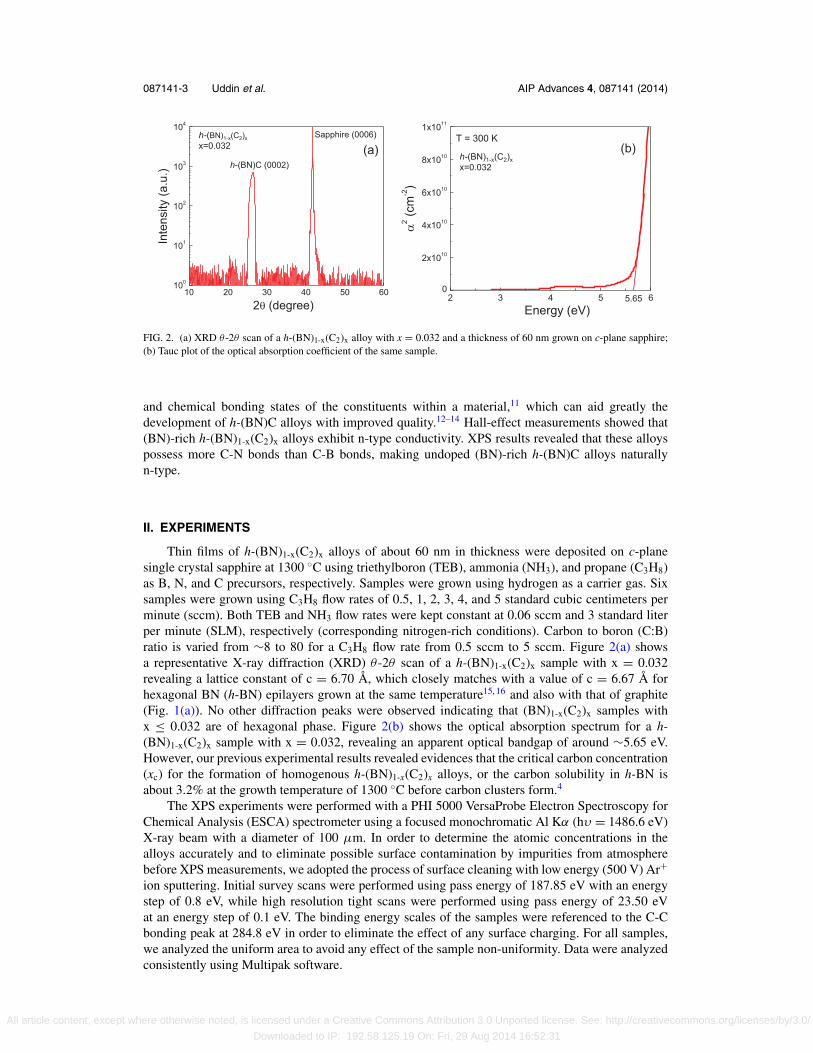
FIG. 2. (a) XRD θ -2θ scan of a h-(BN)1-x(C2)x alloy with x = 0.032 and a thickness of 60 nm grown on c-plane sapphire;(b) Tauc plot of the optical absorption coefficient of the same sample.
and chemical bonding states of the constituents within a material,11 which can aid greatly thedevelopment of h-(BN)C alloys with improved quality.12–14 Hall-effect measurements showed that(BN)-rich h-(BN)1-x(C2)x alloys exhibit n-type conductivity. XPS results revealed that these alloyspossess more C-N bonds than C-B bonds, making undoped (BN)-rich h-(BN)C alloys naturallyn-type.
II. EXPERIMENTS
Thin films of h-(BN)1-x(C2)x alloys of about 60 nm in thickness were deposited on c-planesingle crystal sapphire at 1300 ◦C using triethylboron (TEB), ammonia (NH3), and propane (C3H8)as B, N, and C precursors, respectively. Samples were grown using hydrogen as a carrier gas. Sixsamples were grown using C3H8 flow rates of 0.5, 1, 2, 3, 4, and 5 standard cubic centimeters perminute (sccm). Both TEB and NH3 flow rates were kept constant at 0.06 sccm and 3 standard literper minute (SLM), respectively (corresponding nitrogen-rich conditions). Carbon to boron (C:B)ratio is varied from ∼8 to 80 for a C3H8 flow rate from 0.5 sccm to 5 sccm. Figure 2(a) showsa representative X-ray diffraction (XRD) θ -2θ scan of a h-(BN)1-x(C2)x sample with x = 0.032revealing a lattice constant of c = 6.70 Å, which closely matches with a value of c = 6.67 Å forhexagonal BN (h-BN) epilayers grown at the same temperature15, 16 and also with that of graphite(Fig. 1(a)). No other diffraction peaks were observed indicating that (BN)1-x(C2)x samples withx ≤ 0.032 are of hexagonal phase. Figure 2(b) shows the optical absorption spectrum for a h-(BN)1-x(C2)x sample with x = 0.032, revealing an apparent optical bandgap of around ∼5.65 eV.However, our previous experimental results revealed evidences that the critical carbon concentration(xc) for the formation of homogenous h-(BN)1-x(C2)x alloys, or the carbon solubility in h-BN isabout 3.2% at the growth temperature of 1300 ◦C before carbon clusters form.4
The XPS experiments were performed with a PHI 5000 VersaProbe Electron Spectroscopy forChemical Analysis (ESCA) spectrometer using a focused monochromatic Al Kα (hυ = 1486.6 eV)X-ray beam with a diameter of 100 μm. In order to determine the atomic concentrations in thealloys accurately and to eliminate possible surface contamination by impurities from atmospherebefore XPS measurements, we adopted the process of surface cleaning with low energy (500 V) Ar+
ion sputtering. Initial survey scans were performed using pass energy of 187.85 eV with an energystep of 0.8 eV, while high resolution tight scans were performed using pass energy of 23.50 eVat an energy step of 0.1 eV. The binding energy scales of the samples were referenced to the C-Cbonding peak at 284.8 eV in order to eliminate the effect of any surface charging. For all samples,we analyzed the uniform area to avoid any effect of the sample non-uniformity. Data were analyzedconsistently using Multipak software.
All article content, except where otherwise noted, is licensed under a Creative Commons Attribution 3.0 Unported license. See: http://creativecommons.org/licenses/by/3.0/
Downloaded to IP: 192.58.125.19 On: Fri, 29 Aug 2014 16:52:31
087141-4 Uddin et al. AIP Advances 4, 087141 (2014)
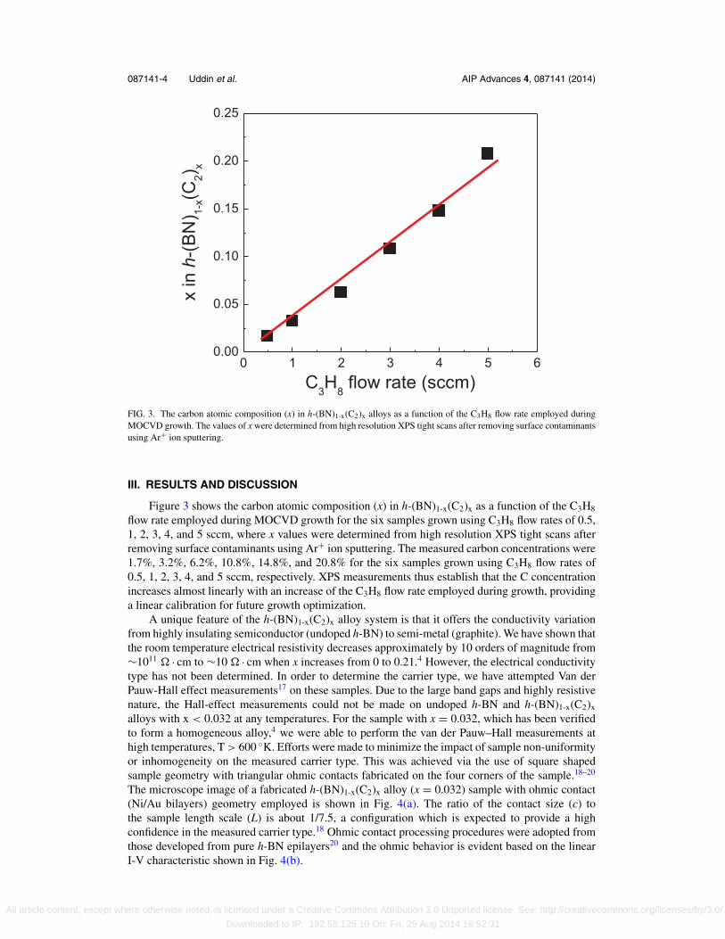
FIG. 3. The carbon atomic composition (x) in h-(BN)1-x(C2)x alloys as a function of the C3H8 flow rate employed duringMOCVD growth. The values of x were determined from high resolution XPS tight scans after removing surface contaminantsusing Ar+ ion sputtering.
III. RESULTS AND DISCUSSION
Figure 3 shows the carbon atomic composition (x) in h-(BN)1-x(C2)x as a function of the C3H8
flow rate employed during MOCVD growth for the six samples grown using C3H8 flow rates of 0.5,1, 2, 3, 4, and 5 sccm, where x values were determined from high resolution XPS tight scans afterremoving surface contaminants using Ar+ ion sputtering. The measured carbon concentrations were1.7%, 3.2%, 6.2%, 10.8%, 14.8%, and 20.8% for the six samples grown using C3H8 flow rates of0.5, 1, 2, 3, 4, and 5 sccm, respectively. XPS measurements thus establish that the C concentrationincreases almost linearly with an increase of the C3H8 flow rate employed during growth, providinga linear calibration for future growth optimization.
A unique feature of the h-(BN)1-x(C2)x alloy system is that it offers the conductivity variationfrom highly insulating semiconductor (undoped h-BN) to semi-metal (graphite). We have shown thatthe room temperature electrical resistivity decreases approximately by 10 orders of magnitude from∼1011 � · cm to ∼10 � · cm when x increases from 0 to 0.21.4 However, the electrical conductivitytype has not been determined. In order to determine the carrier type, we have attempted Van derPauw-Hall effect measurements17 on these samples. Due to the large band gaps and highly resistivenature, the Hall-effect measurements could not be made on undoped h-BN and h-(BN)1-x(C2)x
alloys with x < 0.032 at any temperatures. For the sample with x = 0.032, which has been verifiedto form a homogeneous alloy,4 we were able to perform the van der Pauw–Hall measurements athigh temperatures, T > 600 ◦K. Efforts were made to minimize the impact of sample non-uniformityor inhomogeneity on the measured carrier type. This was achieved via the use of square shapedsample geometry with triangular ohmic contacts fabricated on the four corners of the sample.18–20
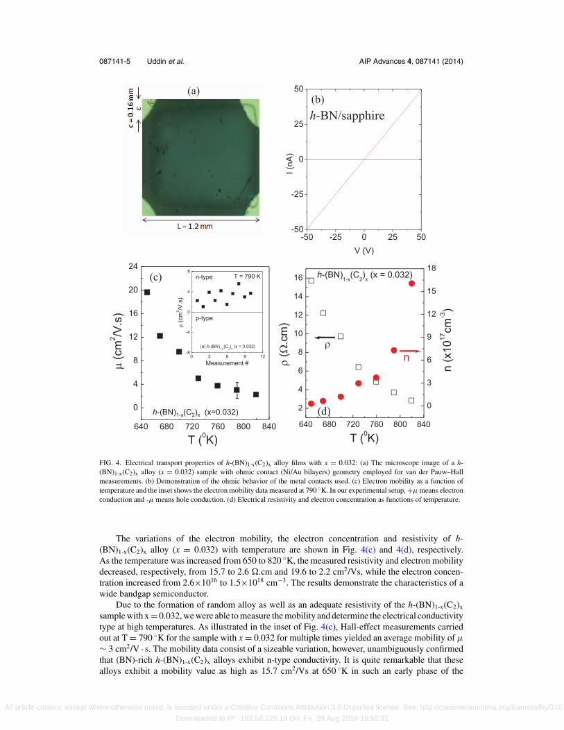
The microscope image of a fabricated h-(BN)1-x(C2)x alloy (x = 0.032) sample with ohmic contact(Ni/Au bilayers) geometry employed is shown in Fig. 4(a). The ratio of the contact size (c) tothe sample length scale (L) is about 1/7.5, a configuration which is expected to provide a highconfidence in the measured carrier type.18 Ohmic contact processing procedures were adopted fromthose developed from pure h-BN epilayers20 and the ohmic behavior is evident based on the linearI-V characteristic shown in Fig. 4(b).
All article content, except where otherwise noted, is licensed under a Creative Commons Attribution 3.0 Unported license. See: http://creativecommons.org/licenses/by/3.0/
Downloaded to IP: 192.58.125.19 On: Fri, 29 Aug 2014 16:52:31
087141-5 Uddin et al. AIP Advances 4, 087141 (2014)
FIG. 4. Electrical transport properties of h-(BN)1-x(C2)x alloy films with x = 0.032: (a) The microscope image of a h-(BN)1-x(C2)x alloy (x = 0.032) sample with ohmic contact (Ni/Au bilayers) geometry employed for van der Pauw–Hallmeasurements. (b) Demonstration of the ohmic behavior of the metal contacts used. (c) Electron mobility as a function oftemperature and the inset shows the electron mobility data measured at 790 ◦K. In our experimental setup, +μ means electronconduction and -μ means hole conduction. (d) Electrical resistivity and electron concentration as functions of temperature.
The variations of the electron mobility, the electron concentration and resistivity of h-(BN)1-x(C2)x alloy (x = 0.032) with temperature are shown in Fig. 4(c) and 4(d), respectively.As the temperature was increased from 650 to 820 ◦K, the measured resistivity and electron mobilitydecreased, respectively, from 15.7 to 2.6 �.cm and 19.6 to 2.2 cm2/Vs, while the electron concen-tration increased from 2.6×10¹⁶ to 1.5×1018 cm−3. The results demonstrate the characteristics of awide bandgap semiconductor.
Due to the formation of random alloy as well as an adequate resistivity of the h-(BN)1-x(C2)x
sample with x = 0.032, we were able to measure the mobility and determine the electrical conductivitytype at high temperatures. As illustrated in the inset of Fig. 4(c), Hall-effect measurements carriedout at T = 790 ◦K for the sample with x = 0.032 for multiple times yielded an average mobility of μ
∼ 3 cm2/V · s. The mobility data consist of a sizeable variation, however, unambiguously confirmedthat (BN)-rich h-(BN)1-x(C2)x alloys exhibit n-type conductivity. It is quite remarkable that thesealloys exhibit a mobility value as high as 15.7 cm2/Vs at 650 ◦K in such an early phase of the
All article content, except where otherwise noted, is licensed under a Creative Commons Attribution 3.0 Unported license. See: http://creativecommons.org/licenses/by/3.0/
Downloaded to IP: 192.58.125.19 On: Fri, 29 Aug 2014 16:52:31

087141-6 Uddin et al. AIP Advances 4, 087141 (2014)
FIG. 5. XPS spectra of C 1s core level for the h-(BN)1-x(C2)x alloy with x = 0.032. The inset are schematic illustrations ofC-N and C-B bonds in (BN)-rich h-(BN)1-x(C2)x alloys.
materials development. In comparison, the highest electron mobility reported for Si doped n–typeAlN, which has a comparable bandgap of about 6 eV, is ∼100 cm2/Vs at 600 K.21
Figure 5 shows XPS spectra of the C 1s core level for h-(BN)1-x(C2)x alloy with x = 0.032. Thespectrum was fitted by subtracting a Shirley background22 with a Gauss-Lorentz function. The peakwas shifted with respect to the fortuitous carbon before any analysis is made. Spectrum 1 showsthe main peak at 284.8 eV, which is similar to that of sp2 bonded C-C (graphite). However, the fullwidth at half maximum (FWHM) of this peak is 1.55 eV, which is significantly higher than ourgraphite (0.70 eV) sample grown under the same conditions. This confirms that there is a significantcontribution from C-B and C-N bonds in this alloy system. Indeed there are two additional peaks inboth sides of the main peak, indicated as spectrum 2 and spectrum 3, respectively. The lower energypeak at 283.3 eV (spectrum 2) is due to C bonding with B (C-B).23–25 The higher energy peak at286.0 eV (spectrum 3) is due to C bonding with N (C-N).26 The chemical shifts, peak broadening,and bonding analysis described above indicate that boron, carbon, and nitrogen atoms bond withone another, and mix atomically.
We believe that the presence of specific bonding states have consequences on the conductivitytype of unintentionally doped (BN)-rich h-(BN)1-x(C2)x alloys. For instances, the observation ofC-N bonds in (BN)-rich h-(BN)C alloys represents the scenario of a fraction of C atoms replacingB (CB), in which C atoms act as n-type dopants. Stated in another way, the detection of C-B bondsin (BN)-rich h-(BN)1-x(C2)x alloys means that a fraction of C atoms are replacing N (CN) and Cact as p-type dopants. Detail studies of the B 1s and N 1s peaks have been carried out and theirbonding states are essential in the understanding of the formation of h-(BN)C alloy.4 However,further analysis of B 1s and N 1s spectra does not provide useful information regarding the electricalconductivity type.
For the sample with x = 0.032, C-N peak (286.0 eV) intensity is stronger than the C-B peak(283.3 eV). The corresponding integrated intensity (peak x area) of the C-N peak is about 1.6 timeslarger than the C-B peak. XPS results shown in Fig. 5 thus imply that the films contain more C-Nbonds than C-B bonds, which means that more C atoms are replacing B than those replacing N,which may account for the observed n-type conductivity in (BN)-rich h-(BN)1-x(C2)x alloys. Thisinterpretation is also consistent with the understanding from the point of view of bond energies
All article content, except where otherwise noted, is licensed under a Creative Commons Attribution 3.0 Unported license. See: http://creativecommons.org/licenses/by/3.0/
Downloaded to IP: 192.58.125.19 On: Fri, 29 Aug 2014 16:52:31
087141-7 Uddin et al. AIP Advances 4, 087141 (2014)
among different bonds in h-(BN)1-x(C2)x alloy: B-N (4.00 eV) > C-C (3.71 eV) > C-N (2.83 eV)> C-B (2.59 eV) > B-B (2.32 eV) > N-N (2.11 eV). The formation of C-N bonds is more favorablethan the formation of C-B bonds due to the larger bond energy of C-N bond.27 Although most Catoms incorporate into h-(BN)1-x(C2)x alloys as pairs due to the relatively large C-C bond energy,from the statistics point of view, there is always a certain fraction of C remains in the isolated state,which can either replace B to provide n-type dopants or replace N to provide p-type dopants. Fromthe formation energy point of view, the formation of C-N bond is also more favorable over that of C-Bbond.27 The presence of more C-N bonds than C-B bonds makes undoped (BN)-rich h-(BN)1-x(C2)x
semiconductor alloys n-type. Thus the XPS results corroborate the mobility data shown in Fig. 4. Avery small fraction of excess C-N bonds (∼1019/1022) can have a significant effect on the electricalconductivity type but not on the variation in composition. Therefore, it is difficult to detect andquantity the variation in composition due to the presence of excess C-N bonds.
IV. CONCLUSIONS
In summary, thin films of (BN)-rich h-(BN)1-x(C2)x semiconductor alloys were synthesized byMOCVD. Hall-effect measurements revealed that these alloys are naturally n-type exhibiting anelectron mobility of about 20 cm2/Vs at 650 ◦K. XPS results indicated that the carbon concentrationin the alloys increases almost linearly with the flow rate of the carbon precursor employed duringthe MOCVD growth, providing a useful calibration for targeted alloy compositions. XPS chemicalbonding analysis revealed that these MOCVD grown alloy films contain more C-N bonds than C-Bbonds, making (BN)-rich h-(BN)1-x(C2)x alloys naturally n-type. Currently, our understanding ofh-(BN)1-x(C2)x alloy is still in a very early stage. XPS studies coupled with optical and transportmeasurements are useful for providing insights into further developing strategies to obtain materialswith improved quality and conductivity control as well as the fundamental understanding on thealloy dependence of the band structures, optical and optoelectronic properties of this emerginglayer-structured material system.
ACKNOWLEDGMENTS
This work is supported by NSF (DMR-1206652). Jiang and Lin are grateful to the AT&TFoundation for the support of Ed Whitacre and Linda Whitacre endowed chairs.
1 B. Arnaud, S. Lebegue, P. Rabiller, and M. Alouani, Phys. Rev. Lett. 96, 026402 (2006).2 B. Huang, X. K. Cao, H. X. Jiang, J. Y. Lin, and S. H. Wei, Physical Review B 86, 155202 (2012).3 X. K. Cao, B. Clubine, J. H. Edgar, J. Y. Lin, and H. X. Jiang, Appl. Phys. Lett. 103, 191106 (2013).4 M. R. Uddin, S. Majety, J. Li, J. Y. Lin, and H. X. Jiang, J. Appl. Phys. 115, 093509 (2014).5 S. Nakamura, G. Fasol, and S. J. Pearton, The Blue Laser Diode: The Complete Story, (Springer, New York, 2000).6 J. Wu, J. Appl. Phys., 106, 011101 (2009).7 M. O. Watanabe, S. Itoh, T. Sasaki, and K. Mizushima, Phys. Rev. Lett. 77, 187 (1996).8 M. O. Watanabe, K. Mizushima, S. Itoh, and M. Mashita, “Semiconductor device using semiconductor BCN compounds,”
U.S. patent 5,895, 938.9 S. Umeda, T. Yuki, T. Sugiyama, and T. Sugino, Diamond Relat. Mater. 13, 1135 (2004).
10 M. O. Watanabe, S. Itoh, K. Mizushima, and T. Sasaki, J. Appl. Phys. 78, 2880 (1995).11 D. Briggs and M. P. Seah, Practical surface analysis by Auger and X-ray photoelectron spectroscopy (Wiley, New York,
1990).12 J. R. Martins and H. Chacham, ACS Nano 5, 385 (2011).13 M. O. Watanabe, S. Itoh, K. Mizushima, and T. Sasaki, Appl. Phys. Lett. 68, 2962 (1996).14 V. Linss, S. E. Rodil, P. Reinke, M. G. Garnier, P. Oelhafen, U. Kreissig, and F. Richter, Thin Solid Films 467, 76 (2004).15 R. Dahal, J. Li, S. Majety, B. N. Pantha, X. K. Cao, J. Y. Lin, and H. X. Jiang, Appl. Phys. Lett. 98, 211110 (2011).16 J. Li, S. Majety, R. Dahal, W. P. Zhao, J. Y. Lin, and H. X. Jiang, Appl. Phys. Lett. 101, 171112 (2012).17 L. J. Van der Pauw, Philips Research Reports, 13, 1 (1958).18 O. Bierwagen, T. Ive, C. G. Van de Walle, and J. S. Speck, Appl. Phys. Lett. 93, 242108 (2008).19 A. Kumar, J. Pernot, F. Omnes, P. Muret, A. Traore, L. Magaud, A. Deneuville, N. Habka, J. Barjon, F. Jomard, M. A.
Pinault, J. Chevallier, C. Mer-Calfati, J. C. Arnault, and P. Bergonzo, J. Appl. Phys. 110, 033718 (2011).20 S. Majety, T. C. Doan, J. Li, J. Y. Lin, and H. X. Jiang, AIP Advances 3, 122116 (2013).21 Y. Taniyasu, M. Kasu, and T. Makimoto, Nature, 441, 325 (2006).22 D. A. Shirley, Phys. Rev. B 5, 4709 (1972).23 H. Kunzli, P. Gantenbein, R. Steiner, and P. Oelhafen, Anal. Chem. 346, 41 (1993).
All article content, except where otherwise noted, is licensed under a Creative Commons Attribution 3.0 Unported license. See: http://creativecommons.org/licenses/by/3.0/
Downloaded to IP: 192.58.125.19 On: Fri, 29 Aug 2014 16:52:31

087141-8 Uddin et al. AIP Advances 4, 087141 (2014)
24 H. A. Castillo, P. J. Arango, J. M. Velez, E. Restrepo-Parra, G. Soto, and W. D. la Cruz, Surf. Coat. Technol. 204, 4051(2010).
25 J. Yue, W. Cheng, X. Zhang, D. He, and G. Chen, Thin Solid Films 375, 247 (2000).26 E. G. Wang, Prog. Mater. Sci. 41, 241 (1997).27 M. S. C. Mazzoni, R. W. Nunes, S. Azedevo, and H. Chacham, Phys. Rev. B 73, 073108 (2006).
All article content, except where otherwise noted, is licensed under a Creative Commons Attribution 3.0 Unported license. See: http://creativecommons.org/licenses/by/3.0/
Downloaded to IP: 192.58.125.19 On: Fri, 29 Aug 2014 16:52:31