
ELECTRICAL SIMULATION - GRIET · GRIET/EEE DEPT Electrical Lab Manual II YEAR I SEM EEE By Ms ......
80
ELECTRICAL SIMULATION LAB MANUAL
Transcript of ELECTRICAL SIMULATION - GRIET · GRIET/EEE DEPT Electrical Lab Manual II YEAR I SEM EEE By Ms ......
ELECTRICAL SIMULATION
LAB MANUAL

GRIET/EEE DEPT
Lab Manual
II YEAR I SEM
EEE
By
Ms. Y.Satyavani Assistant Professor, EEE
Ms. V.Usha Assistant Professor, EEE
Department of Electrical and Electronics Engineering
Gokaraju Rangaraju Institute of Engineering & Technology (Autonomous)
BACHUPALLY, MIYAPUR, HYDERABAD-500090
Electrical Simulation Lab
ELECTRICAL SIMULATION LAB

GRIET/EEE DEPT Matlab/Labview Lab
Gokaraju Rangaraju Institute of Engineering & Technology (Autonomous)
Bachupally, Kukatpally
HYDERABAD 500090.
CERTIFICATE
This is to certify that it is a Bonafide Record of practical work done in the Matlab/Labview Laboratory in I sem of II Year during the year.…………….…………
Name: ……………………………………………………..
Roll no: …………………………………………………....
Course: B. Tech. ………. Year…… Semester…………
Branch: …………………………………………………...
SIGNATURE OF STAFF MEMBER
Electrical Simualtion Lab Record

GRIET/EEE DEPT
Contents
Matlab: page no
1.Diode Characteristics 1
2.MOSFET Characteristics 6
3.IGBT Characteristics 12
4.Transient Analysis Of Linear Circuit 17
5.Single Phase Half wave Diode Rectifier 23
6.Single Phase Full Wave Diode Bridge Rectifier 27
7.Single Phase Full Wave Diode Bridge Rectifier With LC Filter 31
8.Three Phase Half wave Diode Rectifier 35
9.Starting Of A 5 HP 240V DC Motor With A Three-Step Resistance Starter 39
Labview:
1.Simple Amplitude Measurement 42
2.Buliding Arrays Using For Loop And While Loop 46
3.Random Signal Generation 49
4.Waveform Minimum & Maximum Value Display 55
5.Wave At Interface 58
6.Force Mass Spring Damper 60
7.Matrix Fundamentals 63
8.Simple Pendulum 66
Scilab:
1.Single Phase Half wave Diode Rectifier 69
2.Creating the Vectors 71
Matlab/Labview Lab

GRIET/EEE DEPT Matlab/Labview Lab
COURSE OBJECTIVES
1. To provide students with a strong background on Matlab/Labview softwares.
2. To train the students how to approach for solving engineering problems.
3. To prepare the students to use Matlab/Labview in their project works.
4. To provide a foundation for use of these softwares in real time applications
COURSE OUTCOMES
1. An ability to express programming and simulation for engineering programs.
2. An ability to find importance of these softwares for lab experimentation.
3. Articulate importance of softwares in research by simulation work.
4. An in-depth knowledge of providing virtual instruments on Labview environment.

GRIET/EEE DEPT Matlab/Labview Lab
INDEX
S.No Date Topic Page
no
Signature of the
Faculty
1.
2.
3.
4.
5.
6.
7.
8.
9.
10.
11.
12.
13.
14.
15.
16.
17.
18.
19.

GRIET/EEE DEPT Matlab/Labview Lab
1
1.DIODE CHARACTERISTICS
AIM: To draw the characteristic curves of diode.
APPARATUS: SOFTWARE REQUIRED: MAT LAB SIMULINK
THEORY:
Diodes are active devices constructed to allow current to flow in one direction. The diode
consists of N-type and P-type materials (see diagram shown below).Each of these materials
originally consisted of pure silicon doped to obtain the type of characteristic desired. Doping is the
process of adding impurities to the pure semiconductor material. N-type material is formed when the
impurities with five electrons in the outer most shell (pentavalent) are added to the pure
semiconductor material. Pentavalent materials are elements such as antimony, arsenic, and
phosphorus. The same procedure is then performed for the P-type material using an atom containing
only three electrons in its outer shell (trivalent). Trivalent materials are elements such as boron,
gallium, and indium. A diode is formed when a piece of pure material is doped half as N-type and
half as P-type material. It is not constructed by fusing the N and P type materials together. The N-
type material is called the cathode and the P-type material is called the anode. A junction, called the
depletion region, is formed where the two materials meet. Some of the free electrons begin diffusing
across the junction and fill the holes in the P-type material. When this occurs the atom that the
electron joined becomes a negative ion. When an electron leaves N-type material, it leaves a hole
creating a positive ion. Eventually the diffusion of the free electrons and holes in the junction of the
two materials will decrease to a point where it will stop. The area of positive and negative ions
created around the junction is called the depletion layer. The free electrons in the N-type material are
blocked from diffusing to the P-type material by the negative ions in the P material.

GRIET/EEE DEPT Matlab/Labview Lab
2
Holes from the P material are blocked by the positive ions in the N material. For charge
carriers to flow through the layer, a small voltage potential of approximately 0.7V (silicon) or .3V
(germanium)is required to break it down. This is called the barrier potential.There are two types of
biasing that can be applied to a diode. For a diode to be forward biased, a power supply is connected
with the positive terminal to the P-type material (anode) and the negative terminal to the N-type
material (cathode). As the potential across the diode approaches the barrier, the diode begins
conducting. For a diode to be reversed biased, the power supply leads are set up with the negative
terminal attached to the P-type material and the positive terminal attached to the N-type material.
With this configuration, the electrons in the N-type material and the holes in the P-type material are
drawn away from the depletion layer increasing the width of the layer. Even though the majority
current has stopped flowing, minority current is still flowing due to thermal energy. Minority current
is also called saturation current and can only be increased by an increase in temperature. There is
also a second minute current that flows through the resistive paths created by surface impurities. This
type of current is called surface-leakage current. The sum of saturation current and the surface-
leakage current is called the reverse current.
A diode, such as the silicon diode, will conduct in the reverse bias direction with a significant
amount of voltage applied. At the point of conduction, the diode breaks down resulting in the diode
being damaged. The value of voltage at which the diode breaks down is called the breakdown
voltage. Other types of diodes, such as zener diodes, function in the reverse bias region. The effect of
a zener diode breaking down in the reverse region allows it to be used as a voltage regulator. The
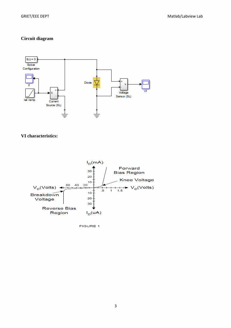
graph of a silicon diode shows the response curve including the forward and reverse bias regions
(See Figure 1 next page). The graph of the silicon diode shows the point in the forward bias region
where the barrier potential is exceeded and the diode begins conduction. The voltage at which the
diode begins conducting is called the knee voltage. In the reverse bias region, the point at which the
diode begins breaking down is also shown. The voltage level at the moment of breakdown is called
the breakdown voltage as mentioned previously
GRIET/EEE DEPT Matlab/Labview Lab
3
Circuit diagram
VI characteristics:

GRIET/EEE DEPT Matlab/Labview Lab
4
Calculations:
GRIET/EEE DEPT Matlab/Labview Lab
5
Graph:
Result:

GRIET/EEE DEPT Matlab/Labview Lab
6
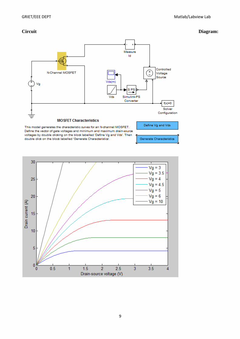
2.MOSFET CHARACTERISTICS
AIM: To draw the characteristic curves for an N-channel MOSFET
APPARATUS: SOFTWARE REQUIRED: MAT LAB SIMULINK
Theory: The metal–oxide–semiconductor field-effect transistor (MOSFET) is a transistor used for
amplifying or switching electronic signals. In MOSFETs, a voltage on the oxide-insulated gate
electrode can induce a conducting channel between the two other contacts called source and drain.
The channel can be of n-type or p-type, and is accordingly called an nMOSFET or a pMOSFET.
Figure 1 shows the schematic diagram of the structure of an nMOS device before and after channel
formation.
Fig. (1a): nMOSFET before channel formation Fig. (1b): nMOSFET structure after channel
formation
GRIET/EEE DEPT Matlab/Labview Lab
7
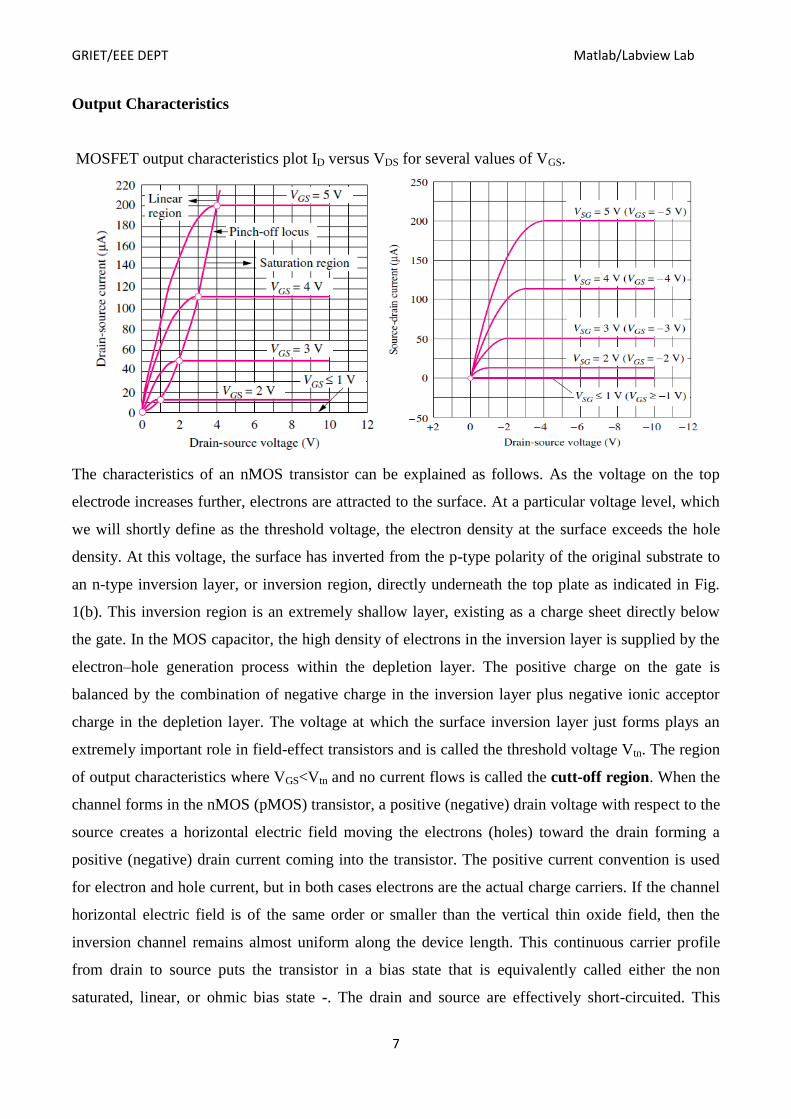
Output Characteristics
MOSFET output characteristics plot ID versus VDS for several values of VGS.
The characteristics of an nMOS transistor can be explained as follows. As the voltage on the top
electrode increases further, electrons are attracted to the surface. At a particular voltage level, which
we will shortly define as the threshold voltage, the electron density at the surface exceeds the hole
density. At this voltage, the surface has inverted from the p-type polarity of the original substrate to
an n-type inversion layer, or inversion region, directly underneath the top plate as indicated in Fig.
1(b). This inversion region is an extremely shallow layer, existing as a charge sheet directly below
the gate. In the MOS capacitor, the high density of electrons in the inversion layer is supplied by the
electron–hole generation process within the depletion layer. The positive charge on the gate is
balanced by the combination of negative charge in the inversion layer plus negative ionic acceptor
charge in the depletion layer. The voltage at which the surface inversion layer just forms plays an
extremely important role in field-effect transistors and is called the threshold voltage Vtn. The region
of output characteristics where VGS<Vtn and no current flows is called the cutt-off region. When the
channel forms in the nMOS (pMOS) transistor, a positive (negative) drain voltage with respect to the
source creates a horizontal electric field moving the electrons (holes) toward the drain forming a
positive (negative) drain current coming into the transistor. The positive current convention is used
for electron and hole current, but in both cases electrons are the actual charge carriers. If the channel
horizontal electric field is of the same order or smaller than the vertical thin oxide field, then the
inversion channel remains almost uniform along the device length. This continuous carrier profile
from drain to source puts the transistor in a bias state that is equivalently called either the non
saturated, linear, or ohmic bias state -. The drain and source are effectively short-circuited. This

GRIET/EEE DEPT Matlab/Labview Lab
8
happens when VGS > VDS + Vtn for nMOS transistor and VGS < VDS +Vtp for pMOS transistor. Drain
current is linearly related to drain-source voltage over small intervals in the linear bias state.
But if the nMOS drain voltage increases beyond the limit, so that VGS < VDS + Vtn, then the
horizontal electric field becomes stronger than the vertical field at the drain end, creating an
asymmetry of the channel carrier inversion distribution
If the drain voltage riseswhile the gate voltage remains the same, then VGD can go below the
threshold voltage in the drain region. There can be no carrier inversion at the drain-gate oxide region,
so the inverted portion of the channel retracts from the drain, and no longer “touches” this terminal.
The pinched-off portion of the channel forms a depletion region with a high electric field. The n-
drain and p-bulk form a pn junction. When this happens the inversion channel is said to be “pinched-
off” and the device is in the saturation region. The characteristics can be loosely modelled by the
following equations.
GRIET/EEE DEPT Matlab/Labview Lab
9
Circuit Diagram:

GRIET/EEE DEPT Matlab/Labview Lab
10
Calculations:

GRIET/EEE DEPT Matlab/Labview Lab
11
Graph:
Result:
GRIET/EEE DEPT Matlab/Labview Lab
12
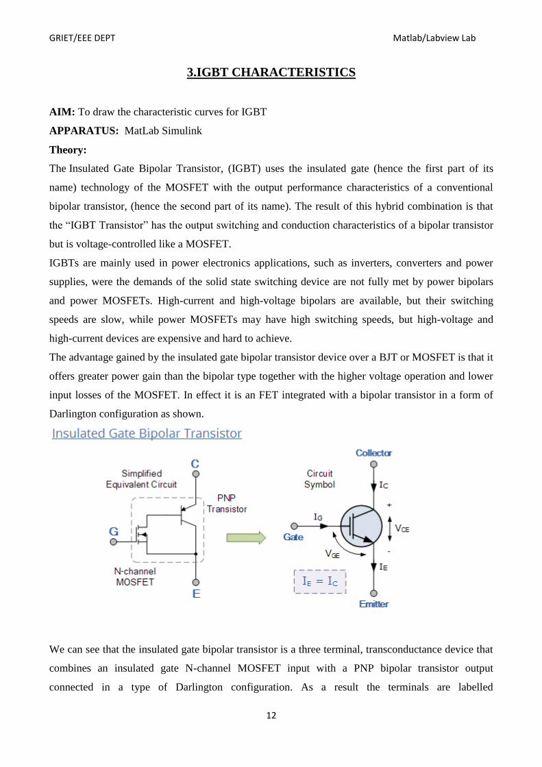
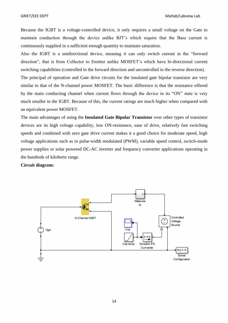
3.IGBT CHARACTERISTICS
AIM: To draw the characteristic curves for IGBT
APPARATUS: MatLab Simulink
Theory:
The Insulated Gate Bipolar Transistor, (IGBT) uses the insulated gate (hence the first part of its
name) technology of the MOSFET with the output performance characteristics of a conventional
bipolar transistor, (hence the second part of its name). The result of this hybrid combination is that
the “IGBT Transistor” has the output switching and conduction characteristics of a bipolar transistor
but is voltage-controlled like a MOSFET.
IGBTs are mainly used in power electronics applications, such as inverters, converters and power
supplies, were the demands of the solid state switching device are not fully met by power bipolars
and power MOSFETs. High-current and high-voltage bipolars are available, but their switching
speeds are slow, while power MOSFETs may have high switching speeds, but high-voltage and
high-current devices are expensive and hard to achieve.
The advantage gained by the insulated gate bipolar transistor device over a BJT or MOSFET is that it
offers greater power gain than the bipolar type together with the higher voltage operation and lower
input losses of the MOSFET. In effect it is an FET integrated with a bipolar transistor in a form of
Darlington configuration as shown.
We can see that the insulated gate bipolar transistor is a three terminal, transconductance device that
combines an insulated gate N-channel MOSFET input with a PNP bipolar transistor output
connected in a type of Darlington configuration. As a result the terminals are labelled

GRIET/EEE DEPT Matlab/Labview Lab
13
as: Collector,Emitter and Gate. Two of its terminals (C-E) are associated with a conductance path
and the third terminal (G) associated with its control.
The amount of amplification achieved by the insulated gate bipolar transistor is a ratio between its
output signal and its input signal. For a conventional bipolar junction transistor, (BJT) the amount of
gain is approximately equal to the ratio of the output current to the input current, called Beta.
For a metal oxide semiconductor field effect transistor or MOSFET, there is no input current as the
gate is isolated from the main current carrying channel. Therefore, an FET’s gain is equal to the ratio
of output current change to input voltage change, making it a transconductance device and this is
also true of the IGBT. Then we can treat the IGBT as a power BJT whose base current is provided by
a MOSFET.
The Insulated Gate Bipolar Transistor can be used in small signal amplifier circuits in much the
same way as the BJT or MOSFET type transistors. But as the IGBT combines the low conduction
loss of a BJT with the high switching speed of a power MOSFET an optimal solid state switch exists
which is ideal for use in power electronics applications.
Also, the IGBT has a much lower “on-state” resistance, RON than an equivalent MOSFET. This
means that the I2R drop across the bipolar output structure for a given switching current is much
lower. The forward blocking operation of the IGBT transistor is identical to a power MOSFET.
When used as static controlled switch, the insulated gate bipolar transistor has voltage and current
ratings similar to that of the bipolar transistor. However, the presence of an isolated gate in an IGBT
makes it a lot simpler to drive than the BJT as much less drive power is needed.
An insulated gate bipolar transistor is simply turned “ON” or “OFF” by activating and deactivating
its Gate terminal. A constant positive voltage input signal across the Gate and the Emitter will keep
the device in its “ON” state, while removal of the input signal will cause it to turn “OFF” in much
the same way as a bipolar transistor or MOSFET.
GRIET/EEE DEPT Matlab/Labview Lab
14
Because the IGBT is a voltage-controlled device, it only requires a small voltage on the Gate to
maintain conduction through the device unlike BJT’s which require that the Base current is
continuously supplied in a sufficient enough quantity to maintain saturation.
Also the IGBT is a unidirectional device, meaning it can only switch current in the “forward
direction”, that is from Collector to Emitter unlike MOSFET’s which have bi-directional current
switching capabilities (controlled in the forward direction and uncontrolled in the reverse direction).
The principal of operation and Gate drive circuits for the insulated gate bipolar transistor are very
similar to that of the N-channel power MOSFET. The basic difference is that the resistance offered
by the main conducting channel when current flows through the device in its “ON” state is very
much smaller in the IGBT. Because of this, the current ratings are much higher when compared with
an equivalent power MOSFET.
The main advantages of using the Insulated Gate Bipolar Transistor over other types of transistor
devices are its high voltage capability, low ON-resistance, ease of drive, relatively fast switching
speeds and combined with zero gate drive current makes it a good choice for moderate speed, high
voltage applications such as in pulse-width modulated (PWM), variable speed control, switch-mode
power supplies or solar powered DC-AC inverter and frequency converter applications operating in
the hundreds of kilohertz range.
Circuit diagram:
GRIET/EEE DEPT Matlab/Labview Lab
15
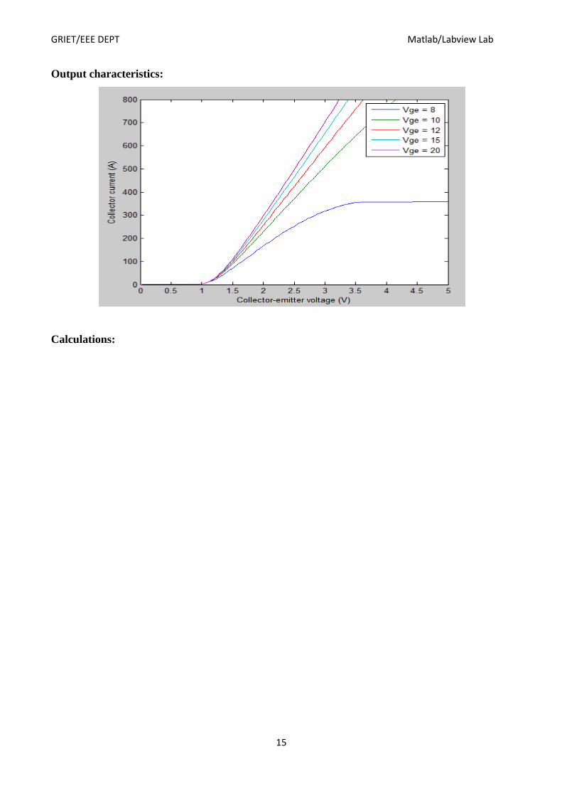
Output characteristics:
Calculations:
GRIET/EEE DEPT Matlab/Labview Lab
16
Graph:
Result:

GRIET/EEE DEPT Matlab/Labview Lab
17
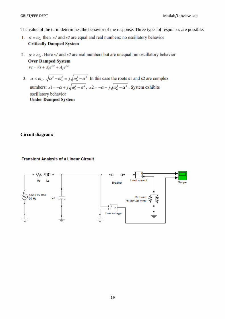
4.Transient analysis of linear circuit
Aim: To observe the transient response of a linear circuit
Apparatus: matlab simulink
Theory:
Series RLC circuit :
The circuit shown on Figure 1 is called the series RLC circuit. We will analyze this
circuit in order to determine its transient characteristics once the switch S is closed
The equation that describes the response of the system is obtained by applying KVL around the mesh
The current flowing in the circuit is
And thus the voltages vR and vL are given by
Substituting Equations (1.3) and (1.4) into Equation (1.1) we obtain The solution to equation (1.5) is
the linear combination of the homogeneous and the particular solution vc =vcp+ vch
The particular solution is

GRIET/EEE DEPT Matlab/Labview Lab
18
Assuming a homogeneous solution is of the form Aset and by substituting into Equation
(1.7) we obtain the characteristic equation
GRIET/EEE DEPT Matlab/Labview Lab
19
The value of the term determines the behavior of the response. Three types of responses are possible:
Circuit diagram:
GRIET/EEE DEPT Matlab/Labview Lab
20
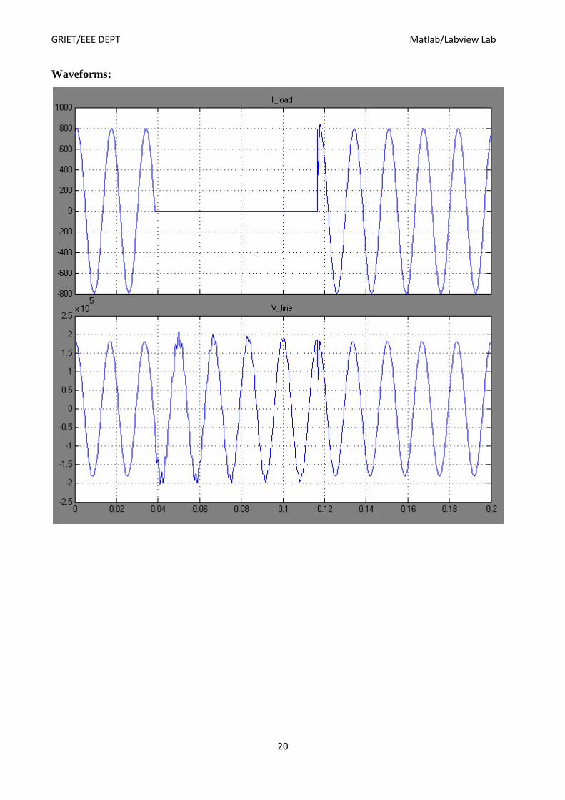
Waveforms:

GRIET/EEE DEPT Matlab/Labview Lab
21
Calculations:

GRIET/EEE DEPT Matlab/Labview Lab
22
Graph:
Result:
GRIET/EEE DEPT Matlab/Labview Lab
23
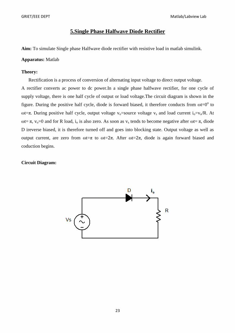
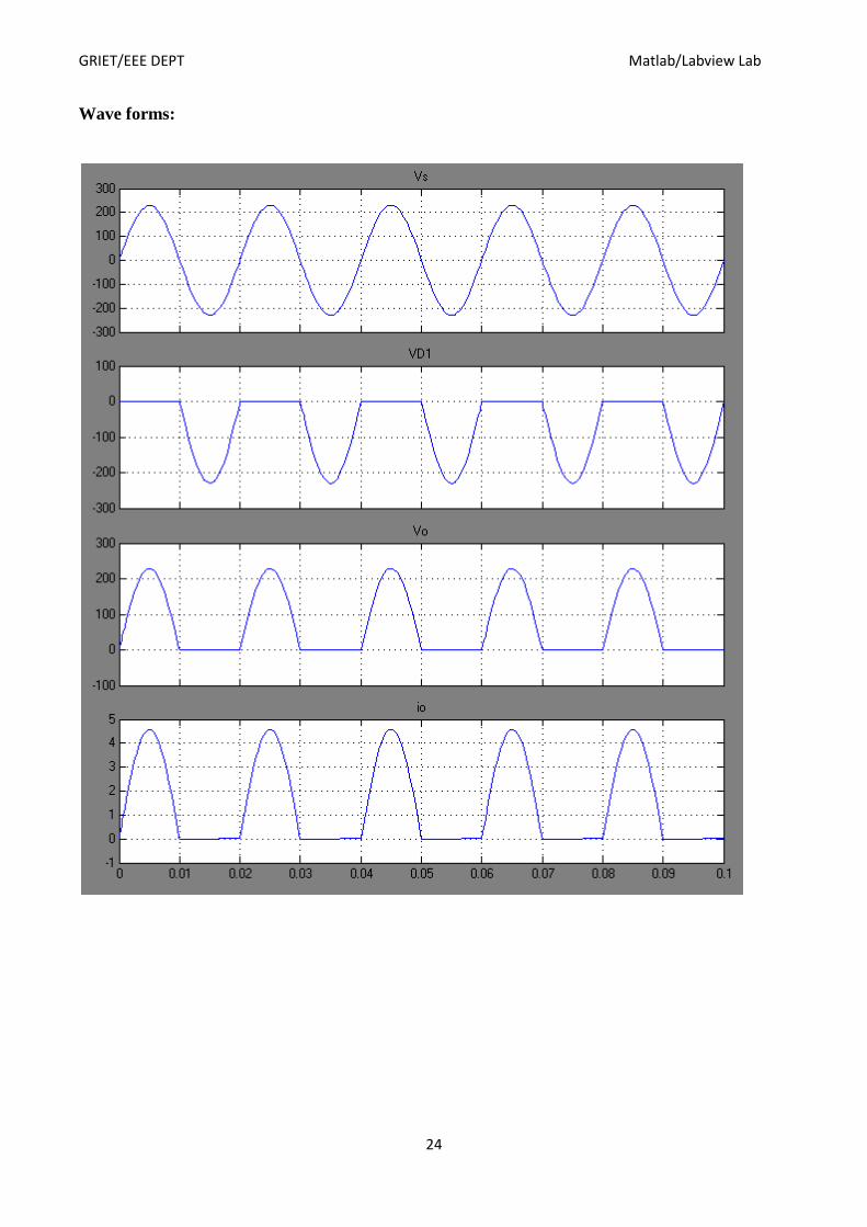
5.Single Phase Halfwave Diode Rectifier
Aim: To simulate Single phase Halfwave diode rectifier with resistive load in matlab simulink.
Apparatus: Matlab
Theory:
Rectification is a process of conversion of alternating input voltage to direct output voltage.
A rectifier converts ac power to dc power.In a single phase halfwave rectifier, for one cycle of
supply voltage, there is one half cycle of output or load voltage.The circuit diagram is shown in the
figure. During the positive half cycle, diode is forward biased, it therefore conducts from t=0o to
t= . During positive half cycle, output voltage vo=source voltage vs and load current io=vo/R. At
t= , vo=0 and for R load, io is also zero. As soon as vs tends to become negative after t= , diode
D ireverse biased, it is therefore turned off and goes into blocking state. Output voltage as well as
output current, are zero from t= to t= . After t= , diode is again forward biased and
coduction begins.
Circuit Diagram:
GRIET/EEE DEPT Matlab/Labview Lab
24
Wave forms:

GRIET/EEE DEPT Matlab/Labview Lab
25
Calculations:

GRIET/EEE DEPT Matlab/Labview Lab
26
Graph:
Result:
GRIET/EEE DEPT Matlab/Labview Lab
27
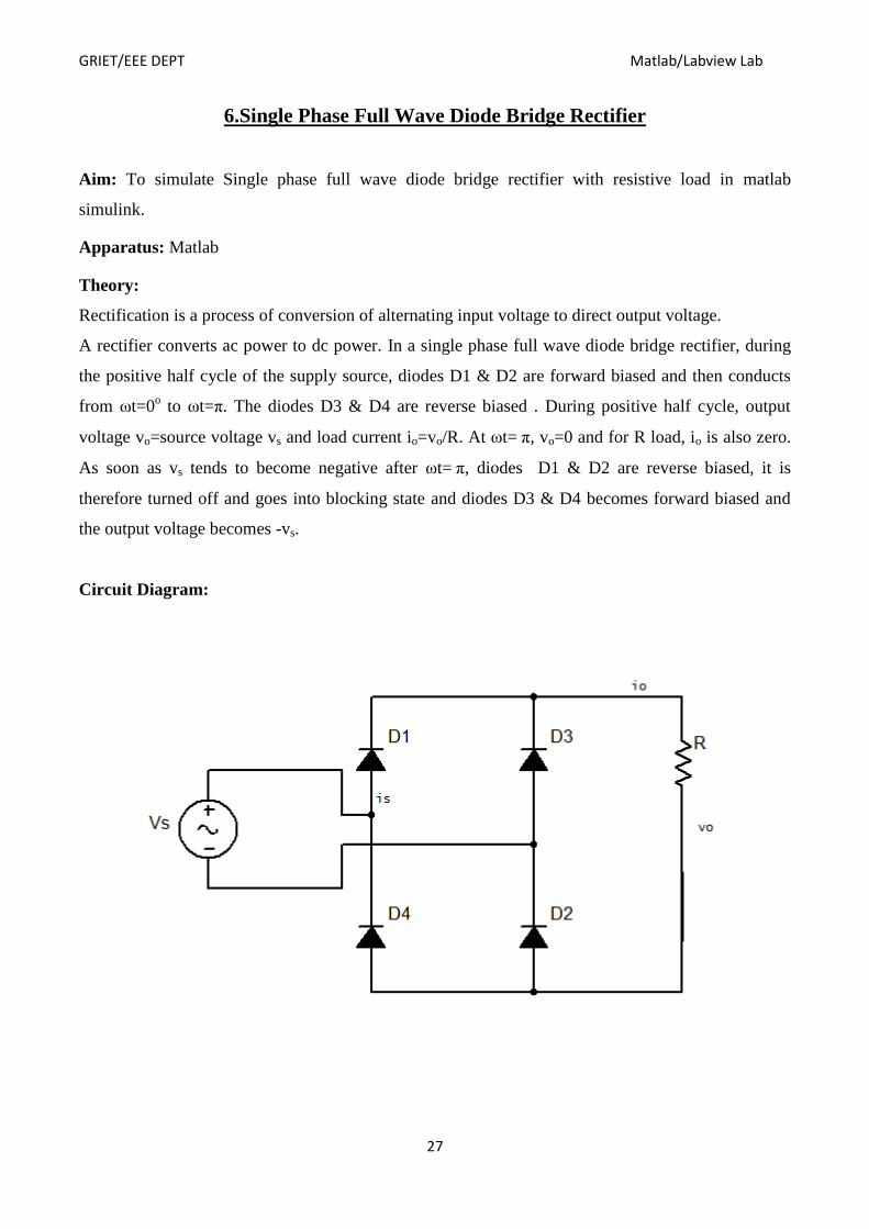
6.Single Phase Full Wave Diode Bridge Rectifier
Aim: To simulate Single phase full wave diode bridge rectifier with resistive load in matlab
simulink.
Apparatus: Matlab
Theory:
Rectification is a process of conversion of alternating input voltage to direct output voltage.
A rectifier converts ac power to dc power. In a single phase full wave diode bridge rectifier, during
the positive half cycle of the supply source, diodes D1 & D2 are forward biased and then conducts
from t=0o to t= . The diodes D3 & D4 are reverse biased . During positive half cycle, output
voltage vo=source voltage vs and load current io=vo/R. At t= , vo=0 and for R load, io is also zero.
As soon as vs tends to become negative after t= , diodes D1 & D2 are reverse biased, it is
therefore turned off and goes into blocking state and diodes D3 & D4 becomes forward biased and
the output voltage becomes -vs.
Circuit Diagram:

GRIET/EEE DEPT Matlab/Labview Lab
28
Wave forms:

GRIET/EEE DEPT Matlab/Labview Lab
29
Calculations:
GRIET/EEE DEPT Matlab/Labview Lab
30
Graph:
Result:
GRIET/EEE DEPT Matlab/Labview Lab
31
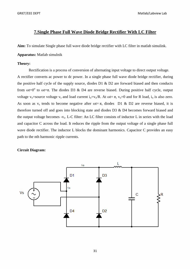
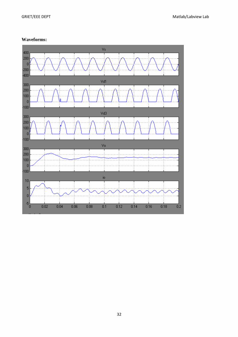
7.Single Phase Full Wave Diode Bridge Rectifier With LC Filter
Aim: To simulate Single phase full wave diode bridge rectifier with LC filter in matlab simulink.
Apparatus: Matlab simulnik
Theory:
Rectification is a process of conversion of alternating input voltage to direct output voltage.
A rectifier converts ac power to dc power. In a single phase full wave diode bridge rectifier, during
the positive half cycle of the supply source, diodes D1 & D2 are forward biased and then conducts
from t=0o to t= . The diodes D3 & D4 are reverse biased. During positive half cycle, output
voltage vo=source voltage vs and load current io=vo/R. At t= , vo=0 and for R load, io is also zero.
As soon as vs tends to become negative after t= , diodes D1 & D2 are reverse biased, it is
therefore turned off and goes into blocking state and diodes D3 & D4 becomes forward biased and
the output voltage becomes -vs. L-C filter: An LC filter consists of inductor L in series with the load
and capacitor C across the load. It reduces the ripple from the output voltage of a single phase full
wave diode rectifier. The inductor L blocks the dominant harmonics. Capacitor C provides an easy
path to the nth harmonic ripple currents.
Circuit Diagram:
GRIET/EEE DEPT Matlab/Labview Lab
32
Waveforms:

GRIET/EEE DEPT Matlab/Labview Lab
33
Calculations:

GRIET/EEE DEPT Matlab/Labview Lab
34
Graph:
Result:

GRIET/EEE DEPT Matlab/Labview Lab
35
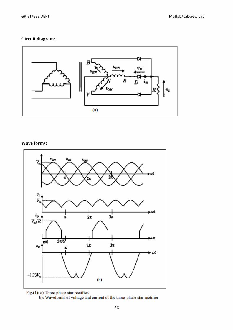
8.Three Phase Halfwave Diode Rectifier
Aim: To simulate Three phase halfwave diode rectifier in matlab simulink.
Apparatus: Matlab simulink
Theory:
Rectification is the process of conversion of alternating input voltage to direct output voltage.
In diode rectifiers, the output voltage cannot be controlled. Three-Phase Half-Wave Rectifier
For higher power application and where three-phase power supply is available, a three phase bridge
rectifier, as shown in figure (1), should be used. One diode is conduct at any instant. It is the diode
connected to the phase having the highest instantaneous voltage. The output voltage of the
successive phase voltages and varying from Vm/2 to Vm, three times per input cycle. The average
output voltage is:.
Similarly, the rms value of the output voltage can be found as:
The rectifier has a three pulse characteristics, and load current id of less ripple contents in relative to
single-phase rectifiers, which characterize by two pulse output. The ripple frequency is 3f (where f is
input frequency) and the required smoothing reactor at the load side is of smaller size.
GRIET/EEE DEPT Matlab/Labview Lab
36
Circuit diagram:
Wave forms:

GRIET/EEE DEPT Matlab/Labview Lab
37
Calculations:

GRIET/EEE DEPT Matlab/Labview Lab
38
Graph:
Result:

GRIET/EEE DEPT Matlab/Labview Lab
39
9.Starting Of A 5 HP 240V DC Motor With A Three-Step Resistance Starter
Aim: To simulate Starting of a 5 HP 240V DC motor with a three-step resistance starter.
Apparatus: Matlab simulink
Theory:
Starting Methods of A DC Motor
Basic operational voltage equation of a DC motor is given as
E = Eb + IaRa and hence Ia = (E - Eb) / Ra
Now, when the motor is at rest, obviously, there is no back emf Eb, hence armature current
will be high at starting. This excessive current will-
1. blow out the fuses and may damage the armature winding and/or commutator brush arrangement.
2. produce very high starting torque (as torque is directly proportional to armature current), and this
high starting toque will produce huge centrifugal force which may throw off the armature windings.
Thus to avoid above two drawbacks, starters are used for starting of DC machine.
Thus, to avoid the above dangers while starting a DC motor, it is necessary to limit the
starting current. For that purpose, starters are used to start a DC motor. There are various starters
like, 3 point starter, 4 point starter, No load release coil starter, thyristor starter etc.
The main concept behind every DC motor starter is, adding external resistance to the armature
winding at starting.
Ciruit diagram:

GRIET/EEE DEPT Matlab/Labview Lab
40
Plot:
Calculations:

GRIET/EEE DEPT Matlab/Labview Lab
41
Graph:
Result:
GRIET/EEE DEPT Matlab/Labview Lab
42
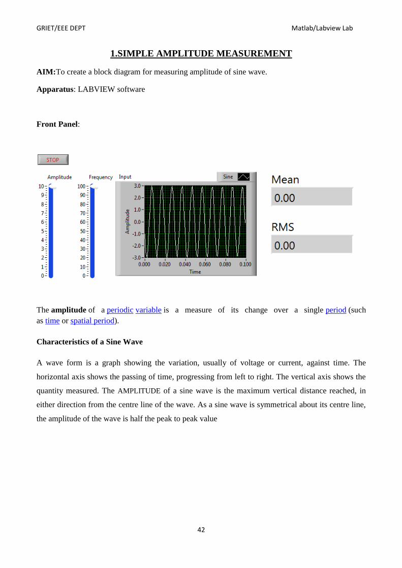
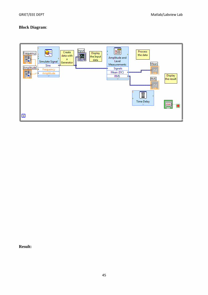
1.SIMPLE AMPLITUDE MEASUREMENT
AIM:To create a block diagram for measuring amplitude of sine wave.
Apparatus: LABVIEW software
Front Panel:
The amplitude of a periodic variable is a measure of its change over a single period (such
as time or spatial period).
Characteristics of a Sine Wave
A wave form is a graph showing the variation, usually of voltage or current, against time. The
horizontal axis shows the passing of time, progressing from left to right. The vertical axis shows the
quantity measured. The AMPLITUDE of a sine wave is the maximum vertical distance reached, in
either direction from the centre line of the wave. As a sine wave is symmetrical about its centre line,
the amplitude of the wave is half the peak to peak value
GRIET/EEE DEPT Matlab/Labview Lab
43
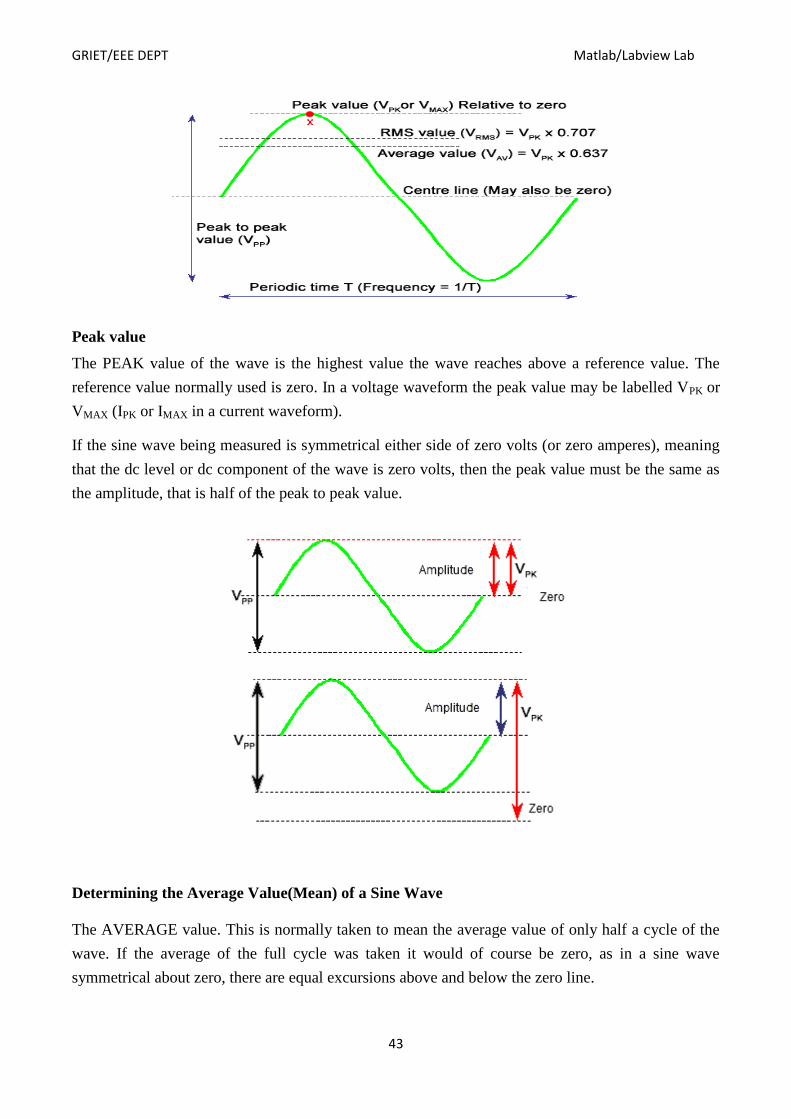
Peak value
The PEAK value of the wave is the highest value the wave reaches above a reference value. The
reference value normally used is zero. In a voltage waveform the peak value may be labelled VPK or
VMAX (IPK or IMAX in a current waveform).
If the sine wave being measured is symmetrical either side of zero volts (or zero amperes), meaning
that the dc level or dc component of the wave is zero volts, then the peak value must be the same as
the amplitude, that is half of the peak to peak value.
Determining the Average Value(Mean) of a Sine Wave
The AVERAGE value. This is normally taken to mean the average value of only half a cycle of the
wave. If the average of the full cycle was taken it would of course be zero, as in a sine wave
symmetrical about zero, there are equal excursions above and below the zero line.

GRIET/EEE DEPT Matlab/Labview Lab
44
Using only half a cycle, as illustrated in fig the average value (voltage or current) is always 0.637 of
the peak value of the wave.
VAV = VPK x 0.637
or
IAV = IPK X 0.637
The RMS Value
The RMS or ROOT MEAN SQUARED value is the value of the equivalent direct (non varying)
voltage or current which would provide the same energy to a circuit as the sine wave measured. That
is, if an AC sine wave has a RMS value of 240 volts, it will provide the same energy to a circuit as a
DC supply of 240 volts.
It can be shown that the RMS value of a sine wave is 0.707 of the peak value.
VRMS = VPK x 0.707 and IRMS = IPK x 0.707
Also, the peak value of a sine wave is equal to 1.414 x the RMS value.
GRIET/EEE DEPT Matlab/Labview Lab
45
Block Diagram:
Result:

GRIET/EEE DEPT Matlab/Labview Lab
46
2.BULIDING ARRAYS USING FOR LOOP AND WHILE LOOP
Aim: To bulid an array using FOR loop and WHILE loop
Apparatus: LABVIEW software
Front Panel:
Working and manipulating with Arrays is an important part in LabVIEW development. Arrays are
very powerful to use in LabVIEW. In all your applications you would probably use both One-
Dimensional Arrays and Two-Dimensional Arrays.
On the Front Panel using the Control palette we can create an array as follows (Array, Matrix &
Cluster subpalette):
You drag and drop the empty Array on the Front Panel, next you find a Control or Indicator
(Numeric, String, Boolean, etc,) and drag it into the empty Array. You can create an Array of
(almost) any kind of Control or Indicator.
2D or multidimensional Array? Just drag the mouse in the Index display to the left and increase the
dimension.

GRIET/EEE DEPT Matlab/Labview Lab
47
On the Block Diagram we have the following Array palette available from the Functions palette in
LabVIEW
Use the Array functions to create and manipulate arrays. The most useful Array functions are
In addition to using loops to read and process elements in an array, you also can use the For Loop
and the While Loop to build arrays. Wire the output of a VI or function in the loop to the loop
border. If you use a While Loop, right-click the resulting tunnel and select Enable Indexing from

GRIET/EEE DEPT Matlab/Labview Lab
48
the shortcut menu. If you use a For Loop, indexing is enabled by default. The output of the tunnel is
an array of every value the VI or function returns after each loop iteration.
The For Loop uses auto-indexing as its default, which is the best method when the number of
values is known. Wire the variable inside the inner loop directly to an array terminal. Since one For
Loop is placed inside another For Loop, a 2D array will be produced.
The While Loop is the best method when the number of values is unknown so the user or
program determines the size of the array. Wire the variable inside the loop directly to an array
terminal. Then right-click on the tunnel and select "enable indexing".
Block Diagram:
Result:
GRIET/EEE DEPT Matlab/Labview Lab
49
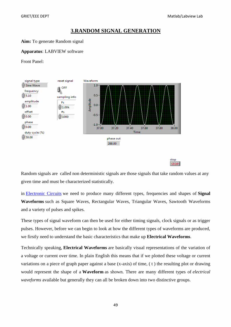
3.RANDOM SIGNAL GENERATION
Aim: To generate Random signal
Apparatus: LABVIEW software
Front Panel:
Random signals are called non deterministic signals are those signals that take random values at any
given time and must be characterized statistically.
in Electronic Circuits we need to produce many different types, frequencies and shapes of Signal
Waveforms such as Square Waves, Rectangular Waves, Triangular Waves, Sawtooth Waveforms
and a variety of pulses and spikes.
These types of signal waveform can then be used for either timing signals, clock signals or as trigger
pulses. However, before we can begin to look at how the different types of waveforms are produced,
we firstly need to understand the basic characteristics that make up Electrical Waveforms.
Technically speaking, Electrical Waveforms are basically visual representations of the variation of
a voltage or current over time. In plain English this means that if we plotted these voltage or current
variations on a piece of graph paper against a base (x-axis) of time, ( t ) the resulting plot or drawing
would represent the shape of a Waveform as shown. There are many different types of electrical
waveforms available but generally they can all be broken down into two distinctive groups.

GRIET/EEE DEPT Matlab/Labview Lab
50
1. Uni-directional Waveforms – these electrical waveforms are always positive or negative in
nature flowing in one forward direction only as they do not cross the zero axis point. Common
uni-directional waveforms include Square-wave timing signals, Clock pulses and Trigger pulses.
2. Bi-directional Waveforms – these electrical waveforms are also called alternating waveforms
as they alternate from a positive direction to a negative direction constantly crossing the zero axis
point. Bi-directional waveforms go through periodic changes in amplitude, with the most
common by far being the Sine-wave.
Whether the waveform is uni-directional, bi-directional, periodic, non-periodic, symmetrical, non-
symmetrical, simple or complex, all electrical waveforms include the following three common
characteristics:
1) Period: – This is the length of time in seconds that the waveform takes to repeat itself from
start to finish. This value can also be called the Periodic Time, ( T ) of the waveform for sine
waves, or the Pulse Width for square waves.
2) Frequency: – This is the number of times the waveform repeats itself within a one second time
period. Frequency is the reciprocal of the time period, ( ƒ = 1/T ) with the standard unit of
frequency being the Hertz, (Hz).
3) Amplitude: – This is the magnitude or intensity of the signal waveform measured in volts or
amps.
Periodic Waveforms
Periodic waveforms are the most common of all the electrical waveforms as it includes Sine
Waves. The AC (Alternating Current) mains waveform in your home is a sine wave and one which
constantly alternates between a maximum value and a minimum value over time.
The amount of time it takes between each individual repetition or cycle of a sinusoidal waveform is
known as its “periodic time” or simply the Period of the waveform. In other words, the time it takes
for the waveform to repeat itself.
Then this period can vary with each waveform from fractions of a second to thousands of seconds as
it depends upon the frequency of the waveform. For example, a sinusoidal waveform which takes
one second to complete its cycle will have a periodic time of one second. Likewise a sine wave
which takes five seconds to complete will have a periodic time of five seconds and so on.
GRIET/EEE DEPT Matlab/Labview Lab
51
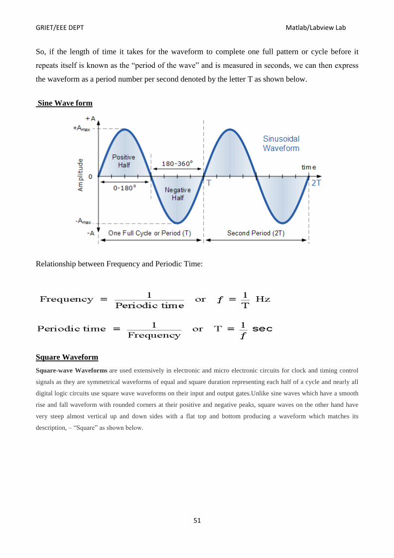
So, if the length of time it takes for the waveform to complete one full pattern or cycle before it
repeats itself is known as the “period of the wave” and is measured in seconds, we can then express
the waveform as a period number per second denoted by the letter T as shown below.
Sine Wave form
Relationship between Frequency and Periodic Time:
Square Waveform
Square-wave Waveforms are used extensively in electronic and micro electronic circuits for clock and timing control
signals as they are symmetrical waveforms of equal and square duration representing each half of a cycle and nearly all
digital logic circuits use square wave waveforms on their input and output gates.Unlike sine waves which have a smooth
rise and fall waveform with rounded corners at their positive and negative peaks, square waves on the other hand have
very steep almost vertical up and down sides with a flat top and bottom producing a waveform which matches its
description, – “Square” as shown below.

GRIET/EEE DEPT Matlab/Labview Lab
52
Rectangular Waveforms
Rectangular Waveforms are similar to the square wave waveform above, the difference being that the two pulse widths
of the waveform are of an unequal time period. Rectangular waveforms are therefore classed as “Non-symmetrical”
waveforms as shown below.
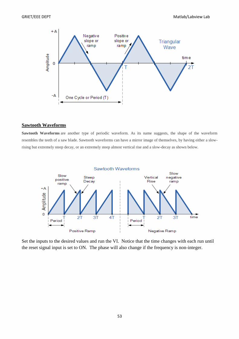
Triangular Waveforms
Triangular Waveforms are generally bi-directional non-sinusoidal waveforms that oscillate between a positive and a
negative peak value. Although called a triangular waveform, the triangular wave is actually more of a symmetrical linear
ramp waveform because it is simply a slow rising and falling voltage signal at a constant frequency or rate. The rate at
which the voltage changes between each ramp direction is equal during both halves of the cycle as shown below.
GRIET/EEE DEPT Matlab/Labview Lab
53
Sawtooth Waveforms
Sawtooth Waveforms are another type of periodic waveform. As its name suggests, the shape of the waveform
resembles the teeth of a saw blade. Sawtooth waveforms can have a mirror image of themselves, by having either a slow-
rising but extremely steep decay, or an extremely steep almost vertical rise and a slow-decay as shown below.
Set the inputs to the desired values and run the VI. Notice that the time changes with each run until
the reset signal input is set to ON. The phase will also change if the frequency is non-integer.
GRIET/EEE DEPT Matlab/Labview Lab
54
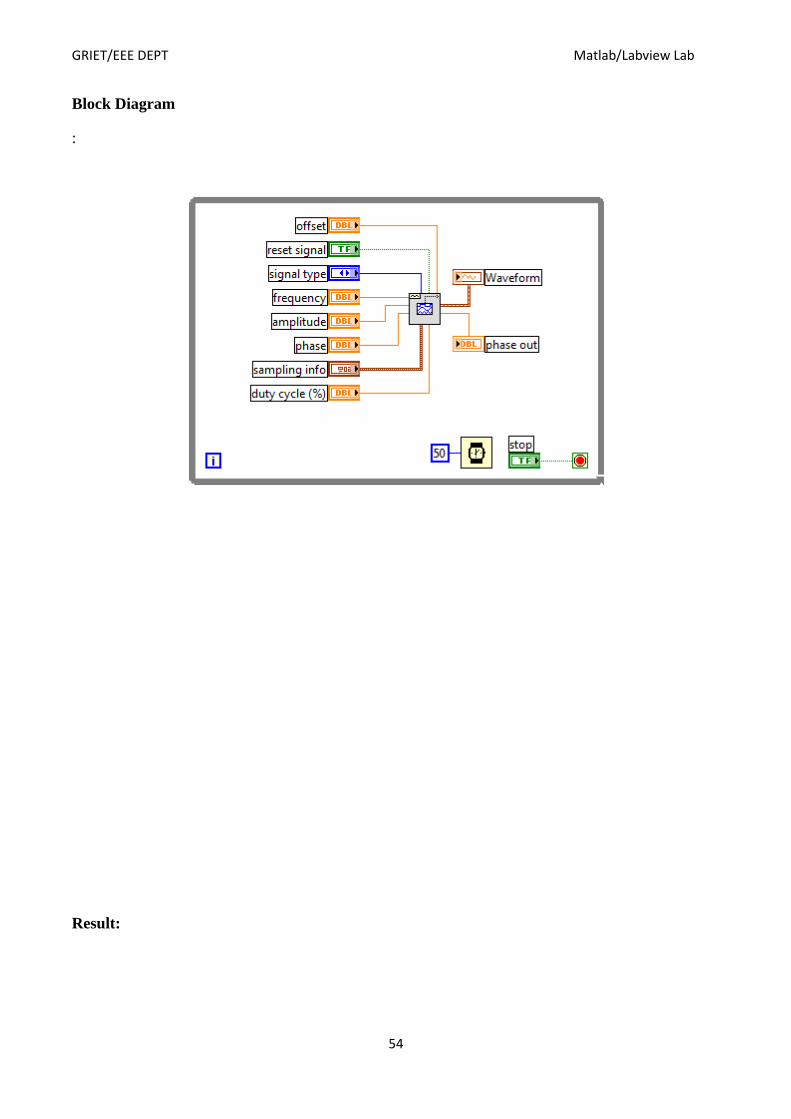
Block Diagram
:
Result:

GRIET/EEE DEPT Matlab/Labview Lab
55
4.WAVEFORM MINIMUM&MAXIMUM VALUE DISPLAY
Aim: To find minimum and maximum value of a given waveform
Apparatus: LABVIEW software
Front Panel:
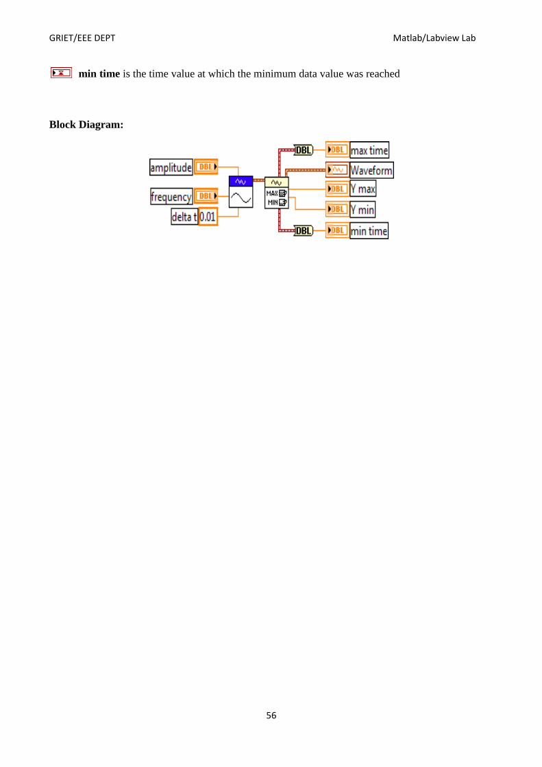
Determines the maximum and minimum values and their associate time values for a waveform.
Enter an amplitude and frequency and run the VI. A sine wave will be generated and the maximum
and minimum values and their positions returned. Note that due to sampling errors, the maximum
and minimum may not be what you expect from the amplitude input.
waveform in is the waveform for which you want to retrieve the maximum and minimum
values.
error in describes error conditions that occur before this node runs. This input
provides standard error infunctionality.
max time is the time value at which the maximum data value was reached.
waveform out returns waveform in unchanged.
Y max is the maximum data value of the waveform.
Y min is the minimum data value of the waveform.
error out contains error information. This output provides standard error out functionality.
GRIET/EEE DEPT Matlab/Labview Lab
56
min time is the time value at which the minimum data value was reached
Block Diagram:

GRIET/EEE DEPT Matlab/Labview Lab
57
Result:
GRIET/EEE DEPT Matlab/Labview Lab
58
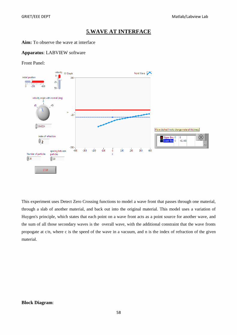
5.WAVE AT INTERFACE
Aim: To observe the wave at interface
Apparatus: LABVIEW software
Front Panel:
This experiment uses Detect Zero Crossing functions to model a wave front that passes through one material,
through a slab of another material, and back out into the original material. This model uses a variation of
Huygen's principle, which states that each point on a wave front acts as a point source for another wave, and
the sum of all those secondary waves is the overall wave, with the additional constraint that the wave fronts
propogate at c/n, where c is the speed of the wave in a vacuum, and n is the index of refraction of the given
material.
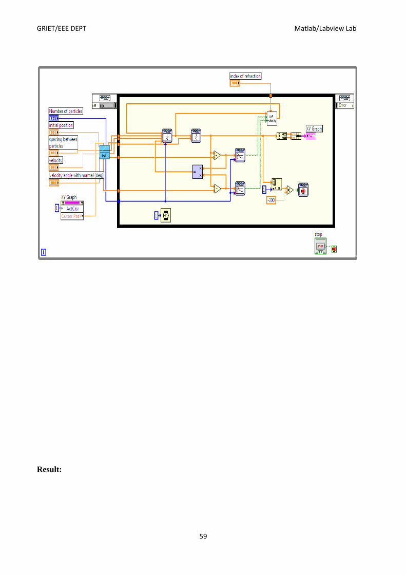
Block Diagram:
GRIET/EEE DEPT Matlab/Labview Lab
59
Result:
GRIET/EEE DEPT Matlab/Labview Lab
60
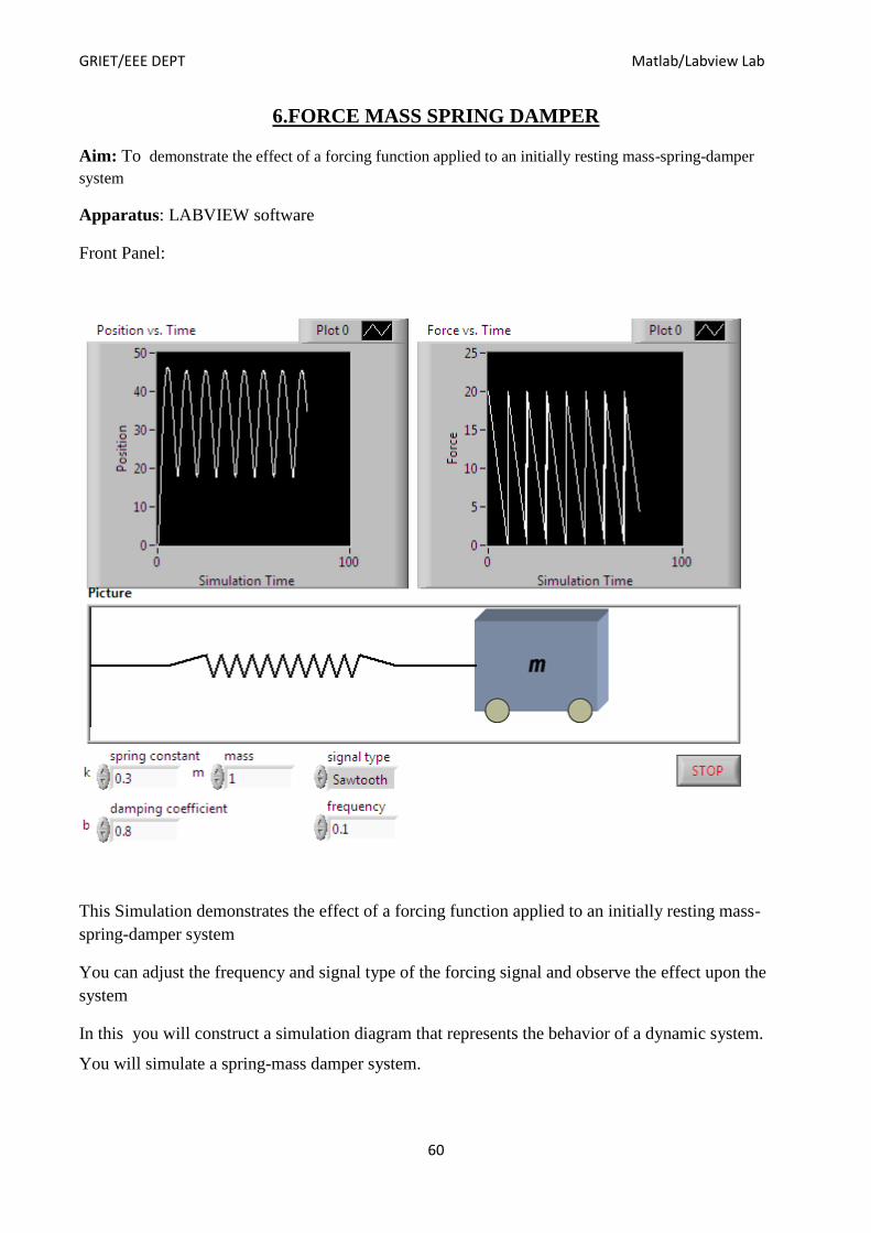
6.FORCE MASS SPRING DAMPER
Aim: To demonstrate the effect of a forcing function applied to an initially resting mass-spring-damper
system
Apparatus: LABVIEW software
Front Panel:
This Simulation demonstrates the effect of a forcing function applied to an initially resting mass-
spring-damper system
You can adjust the frequency and signal type of the forcing signal and observe the effect upon the
system
In this you will construct a simulation diagram that represents the behavior of a dynamic system.
You will simulate a spring-mass damper system.
GRIET/EEE DEPT Matlab/Labview Lab
61
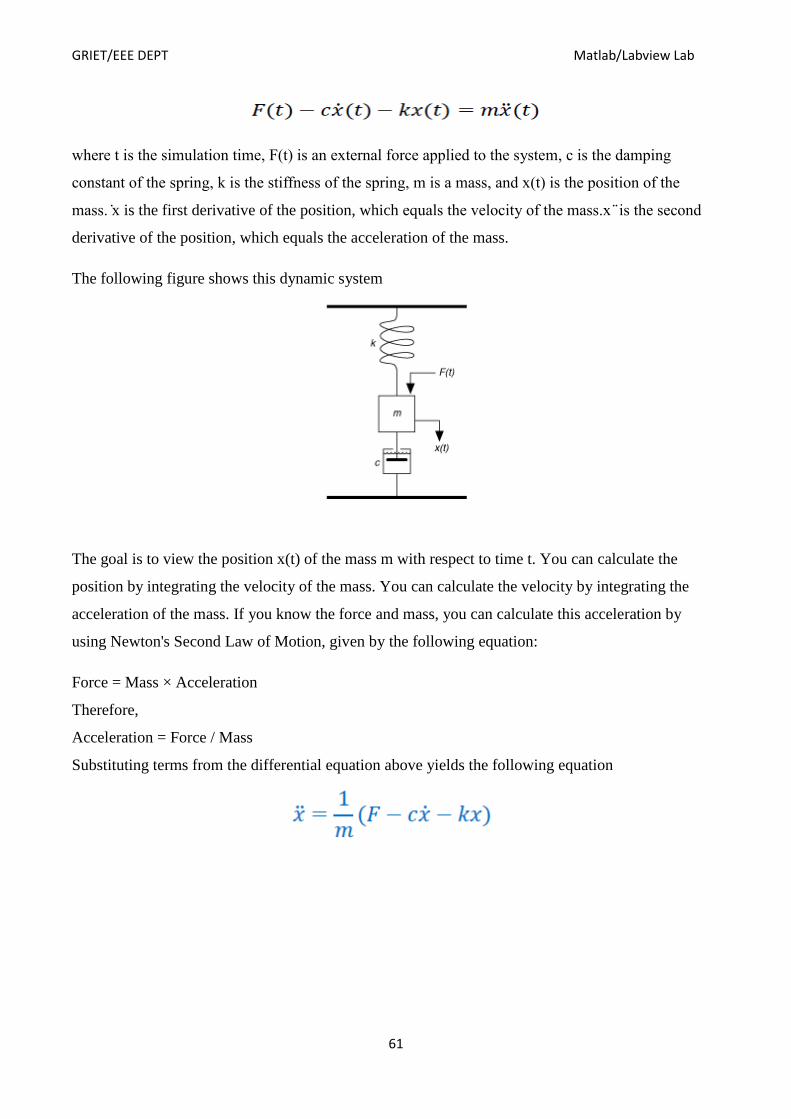
where t is the simulation time, F t is an external force applied to the system, c is the damping
constant of the spring, k is the stiffness of the spring, m is a mass, and x t is the position of the
mass. x is the first derivative of the position, which equals the velocity of the mass.x is the second
derivative of the position, which equals the acceleration of the mass.
The following figure shows this dynamic system
The goal is to view the position x(t) of the mass m with respect to time t. You can calculate the
position by integrating the velocity of the mass. You can calculate the velocity by integrating the
acceleration of the mass. If you know the force and mass, you can calculate this acceleration by
using Newton's Second Law of Motion, given by the following equation:
Force = Mass × Acceleration
Therefore,
Acceleration = Force / Mass
Substituting terms from the differential equation above yields the following equation
GRIET/EEE DEPT Matlab/Labview Lab
62
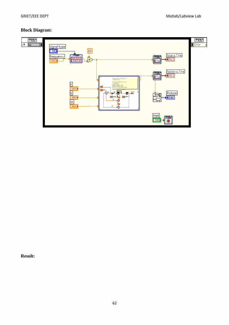
Block Diagram:
Result:

GRIET/EEE DEPT Matlab/Labview Lab
63
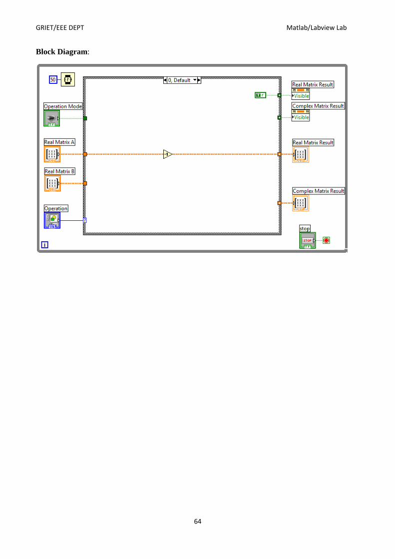
7.MATRIX FUNDAMENTALS
AIM: To learn the fundamentals of matrix.
APPARATUS:LABVIEW
Front Panel:
The following example shows the fundamental behavior and functionality of the matrix data type.
While the test is running, you can change the matrix inputs or select built-in or user-defined numeric
operations. Change the operation mode between matrix and array versions of the operations to see
the difference in results.
Instructions:
1) Run the VI.
2) Modify the inputs, operation and mode, and view the results in the output matrix control.
GRIET/EEE DEPT Matlab/Labview Lab
64
Block Diagram:

GRIET/EEE DEPT Matlab/Labview Lab
65
Result:
GRIET/EEE DEPT Matlab/Labview Lab
66
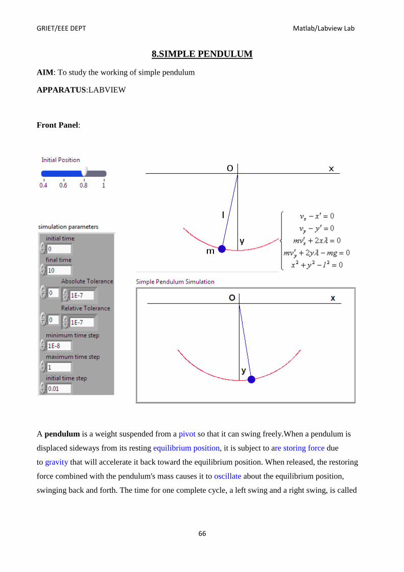
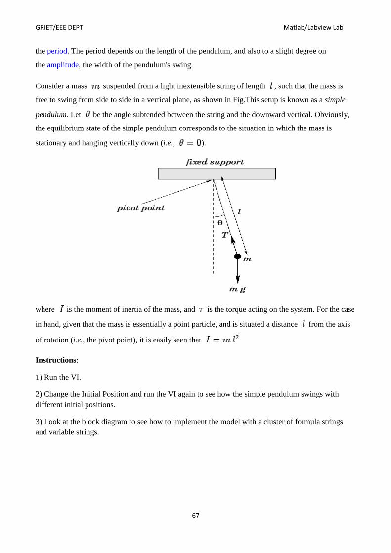
8.SIMPLE PENDULUM
AIM: To study the working of simple pendulum
APPARATUS:LABVIEW
Front Panel:
A pendulum is a weight suspended from a pivot so that it can swing freely.When a pendulum is
displaced sideways from its resting equilibrium position, it is subject to are storing force due
to gravity that will accelerate it back toward the equilibrium position. When released, the restoring
force combined with the pendulum's mass causes it to oscillate about the equilibrium position,
swinging back and forth. The time for one complete cycle, a left swing and a right swing, is called
GRIET/EEE DEPT Matlab/Labview Lab
67
the period. The period depends on the length of the pendulum, and also to a slight degree on
the amplitude, the width of the pendulum's swing.
Consider a mass suspended from a light inextensible string of length , such that the mass is
free to swing from side to side in a vertical plane, as shown in Fig.This setup is known as a simple
pendulum. Let be the angle subtended between the string and the downward vertical. Obviously,
the equilibrium state of the simple pendulum corresponds to the situation in which the mass is
stationary and hanging vertically down (i.e., ).
where is the moment of inertia of the mass, and is the torque acting on the system. For the case
in hand, given that the mass is essentially a point particle, and is situated a distance from the axis
of rotation (i.e., the pivot point), it is easily seen that
Instructions:
1) Run the VI.
2) Change the Initial Position and run the VI again to see how the simple pendulum swings with
different initial positions.
3) Look at the block diagram to see how to implement the model with a cluster of formula strings
and variable strings.

GRIET/EEE DEPT Matlab/Labview Lab
68
Block Diagram:
Result:

GRIET/EEE DEPT Matlab/Labview Lab
69
1.Single phase Halfwave diode rectifier
Aim: To write a program for calculation of parameters of Single phase halfwave diode rectifier
using Sci lab
Apparatus: Sci lab software
Program:
clc;
Vp_sec=230*2^0.5/4;
alph=asind(12/Vp_sec);
alph1=180-alph;
// the di ode w i l l conduc t f rom 8 . 8 9 d e g r e e to 1 7 1 . 5 1 d e g r e e
Angle_conduction=alph1-alph;
printf("ConductionAngle=%2fdegree",Angle_conduction)
Idc=4;
R=1/(2*Idc*%pi)*(2*Vp_sec*cosd(alph)+(2*12*alph*%pi/180)-12*%pi);
printf("\nResistance=%.2fohm",R)
Irms=((1/(2*%pi*R^2))*(((Vp_sec^2/2+12^2)*(%pi-
2*alph*%pi/180))+(Vp_sec^2/2*sind(2*alph))-(4*Vp_sec*12*cosd(alph))))^0.5;
P_rating=Irms^2*R;
printf("\nPowerratingofresistor=%.2fW",P_rating)
Pdc=12*Idc;
t_charging=150/Pdc;
printf("\nChargingtime=%.3fh",t_charging )
Rectifier_efficiency = Pdc/(Pdc+Irms^2*R);
printf("\nRectifierefficiency=%.2f",Rectifier_efficiency )
PIV=Vp_sec+12;
printf("\nPIV=%.3fV",PIV )
Output:
ConductionAngle=163.027726degree Resistance=5.04ohm
Powerratingofresistor=218.51W Chargingtime=3.125h
Rectifierefficiency=0.18 PIV=93.317V

GRIET/EEE DEPT Matlab/Labview Lab
70
Calculations:
Result:

GRIET/EEE DEPT Matlab/Labview Lab
71
2.Creating the vectors
Aim:To create the vectors using scilab commands
Apparatus:Sci lab
Exercise programs:
1.create the vector(x12, x2
2,x3
2,x4
2) with x=1,2,3,4
code: x=1:4;
y=x.^2
Result:
y =
1. 4. 9. 16.
2. create the vector [x1+1, x2+1, x3+1, x4+1] with x=1,2,3,4
code: x=1:4;
y=x+1
Result:
y =
2. 3. 4. 5.
3. Create the vector [x1*y1, x2*y2, x3*y3, x4*y4] with x=1,2,3,4 & y=5,6,7,8
code: x=1:4;
y=5:8;
z=x.*y
Result:
z =
5. 12. 21. 32.
4. Create the vector [x1/y1, x2/y2, x3/y3 ,x4/y4] with x=12*(6:9) & y=1,2,3,4
code: x=12*(6:9);
y=1:4;
z=x./y

GRIET/EEE DEPT Matlab/Labview Lab
72
Result:
z =
72. 42. 32. 27.
5. Create the vector [sin(x1) ,sin(x2) ,sin(x3) ,sin(x4)] with x is a vector of 10 values linearly
chosen in the interval [0,π]
code: x = linspace(0,%pi,10);
y=sin(x)
Result: x=
column 1 to 5
0. 0.3490659 0.6981317 1.0471976 1.3962634
column 6 to 10
1.7453293 2.0943951 2.443461 2.7925268 3.1415927
y =
column 1 to 5
0. 0.3420201 0.6427876 0.8660254 0.9848078
column 6 to 10
0.9848078 0.8660254 0.6427876 0.3420201 1.225D-16
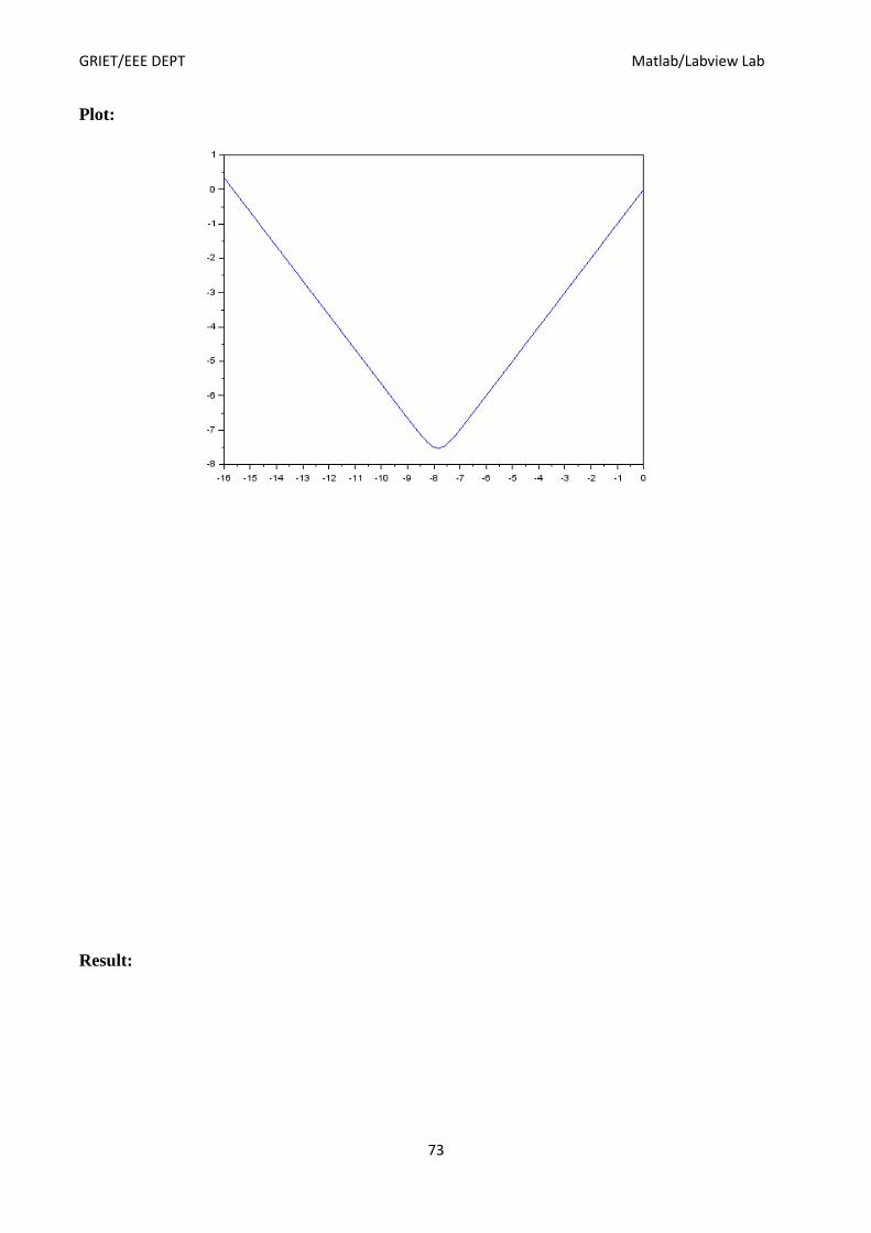
6. compute y=f(x) and Draw the function f(x)=log10(r/10x+ 10
x) with r = 2.220D-16 for x a
vector of 100 values linearly chosen in the interval [-16,0]
code: r = 2.220D-16;
x = linspace (-16,0,100);
y = log10(r./10.^x + 10.^x);
plot(x,y)
GRIET/EEE DEPT Matlab/Labview Lab
73
Plot:
Result:


![A Romantic Jazz Suite [C118] - Free-scores.com : World Free … · eee eee e eee )o 2e %e&o %vq i r x m ± ± m ± ± ± ± ± m ± ± m ± ± ± ± ± " eee eee e eee)o 2e %e&o %vq](https://static.fdocuments.us/doc/165x107/60a6220791891f1ffb1e5d23/a-romantic-jazz-suite-c118-free-world-free-eee-eee-e-eee-o-2e-eo-vq.jpg)