
ELECTRICAL IMPEDANCE TOMOGRAPHY (E.I.T.) MEASUREMENT SYSTEM
102
ELECTRICAL IMPEDANCE TOMOGRAPHY (E.I.T.) MEASUREMENT SYSTEM Ching-Wei, Wesley Chang
Transcript of ELECTRICAL IMPEDANCE TOMOGRAPHY (E.I.T.) MEASUREMENT SYSTEM
ELECTRICAL IMPEDANCE TOMOGRAPHY (E.I.T.)
MEASUREMENT SYSTEM
Ching-Wei, Wesley Chang
2
ELECTRICAL IMPEDANCE TOMOGRAPHY (E.I.T.)
MEASUREMENT SYSTEM
Prepared by:
Ching-Wei, Wesley Chang Fourth Year Student
Department of Electrical Engineering University of Cape Town
Prepared for:
Department of Electrical Engineering University of Cape Town
This thesis was conducted in partial fulfillment of the requirements towards a Bachelor of Science in Electrical Engineering degree at the University of Cape Town.
21 October 2003

3
ACKNOWLEDGEMENTS
I would like to acknowledge my supervisor, Dr A.J. Wilkinson for his expertise and
advice. Through his guidance, I was able to complete this thesis to its specifications.
Thanks also go to Professor J. Greene for his wisdom and excellence in electronics, and
also to Mr. S. Shrire for his contributions.

4
TERMS OF REFERENCE
This project was initiated by Dr. A.J. Wilkinson of the University of Cape Town, on 23
May 2003. A tomography measurement system had been developed to image contents
within a cylindrical rig. This research was initiated to evaluate measurements of the
system which was to be built.
Dr. A.J.Wilkinson’s specific instructions were to:
1. Build a synchronous detection measurement system for electrical impedance
tomography.
2. Build a square-wave driven voltage-to-current converter and characterize its
performance in impedance measurements.
3. Build a sine-wave driven voltage-to-current converter and characterize its
performance in impedance measurements.
4. Obtain measurements at the different outputs of the synchronous detector, and
evaluate them (recover the phase and amplitude difference).
5. Characterize the sensitivity and performance of the system.
6. Draw conclusions on the measurements taken, regarding the effects of different
frequencies implemented on different objects.
7. Make recommendations regarding future project development.
8. Submit the results and all the supporting documentation by 21 October 2003.
5
SYNOPSIS
Process tomography is a technique used to delineate the internal composition of pipes or
mixing vessels without actually having to tamper with the object under investigation.
Process tomography has had many applications since early 1950’s. These varieties of
tomography techniques have been used in both industrial and medical field.
Within the medical field, tomography techniques can be used by placing electrodes to a
patient’s skin surface, and by applying a small current source, images of the human
anatomy can be created. Organs such as lungs, heart, stomach and brain have all been
successfully imaged under research, but this technique has not been accepted as a routine
clinical tool [21].
The topic proposed for this research is an electrical impedance tomography (EIT)
measurement system at a frequency of operation between 1 kHz – 100 kHz. Electrical
impedance tomography is a technique used for imaging the contents of a pipe, vessel or
object. In a typical EIT measurement system, 16 electrodes are mounted on the
circumference of the vessel. Current is injected into the device under test via a pair of
electrodes, and the received signal will be phase shifted. Voltage measurements are
received via a different pair of electrodes and are passed through the demodulation
circuitry (synchronous detector). The synchronous detector should recover the amplitude
and the phase of the signal via a direct measurement of the real and imaginary parts at the
output of the two channels. An image of the internal impedance (conductivity /
permittivity) is constructed from the results obtained. For this project in particular, EIT is
used to determine the impedance profile of various devices under test.
There are two types of drive signals which can be implemented, either a current source or
a voltage source. By using a current driven system, voltage measurements are made on
the sensing side. A voltage measurement with high impedance op-amps will eliminate the
effect of contact impedance on the sensing side. Alternating current is used to combat the
6
effects of polarization which occur at the electrodes. The use of AC also permits
simultaneous measurements of current between several pairs of electrodes by means of
synchronous detection.
Two types of voltage-to-current converters were created, mainly the sine-wave and the
square-wave voltage-to-current converters. Each of these two different applications has
their advantages and their disadvantages. For a square-wave voltage-to-current converter,
frequency of operation was achieved up to 300 kHz. The disadvantage of this system was
that the received signal on the sensing side was also a square-wave; therefore different
filters had to be included in the circuitry which proved to be problematic. By applying a
sine-wave into the device under test, a sine-wave was also received on the sensing side,
therefore no additional circuitry was required for conversion. The main disadvantage of
the sine-wave voltage-to-current converter is that crossover distortions occur, and this
gets worse as the frequency increases.
Electrodes were used for the delivery of the driving signal and also on the sensing side.
Electrodes come in various different shapes and sizes. Some of these aspects have been
investigated in this research. Electrodes utilized for measurements in this research were
mainly 4 electrode plates, implementing the ‘4-electrode technique’, and also a different
arrangement of electrodes, as shown on the left in the figure 8 in chapter 2.3. The
behavior of current density across an electrode depends on the surface area of the
electrode. On the measurement side, measurements are recorded simpler by using thin
‘needle-like’ electrodes for measurement. The type of technique used in this research to
deliver a current source between a pair of electrodes was created by Brown and Seagar
(1987). On the sensing side, a voltage measurement would be measured.
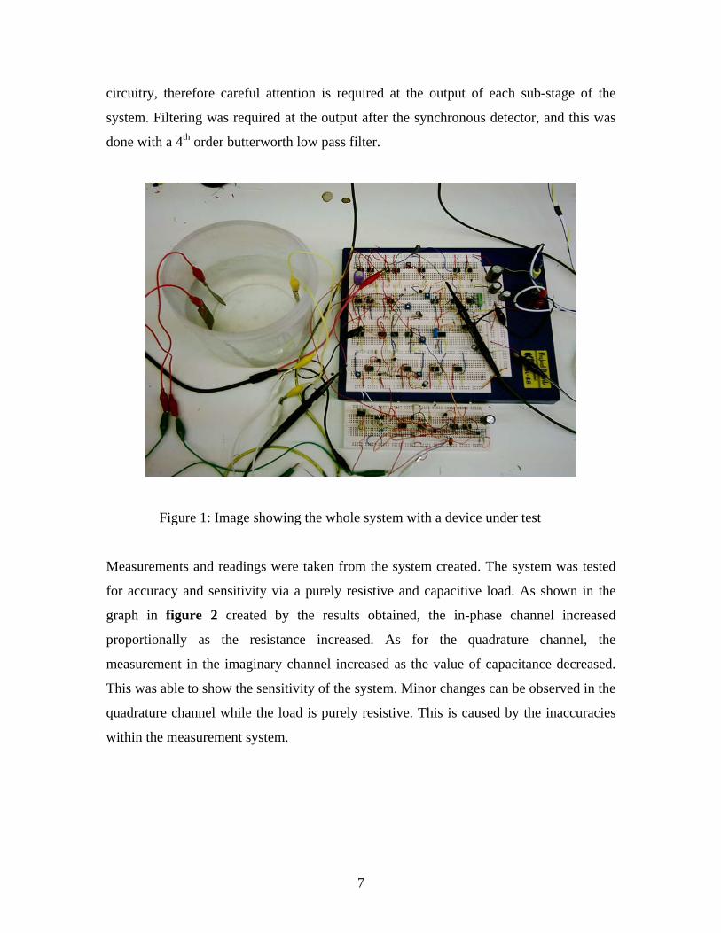
The total system which was created for impedance measurement was made possible by
implementing a synchronous detector (the entire system is shown in figure 1). The type
of synchronous detection implemented is essentially an optional inverter. Two channels
were created to measure the in-phase (real) and quadrature (imaginary) part of the output
signal. Phase shifts and DC offsets occur within the system due to op-amps and other
7
circuitry, therefore careful attention is required at the output of each sub-stage of the
system. Filtering was required at the output after the synchronous detector, and this was
done with a 4th order butterworth low pass filter.
Figure 1: Image showing the whole system with a device under test
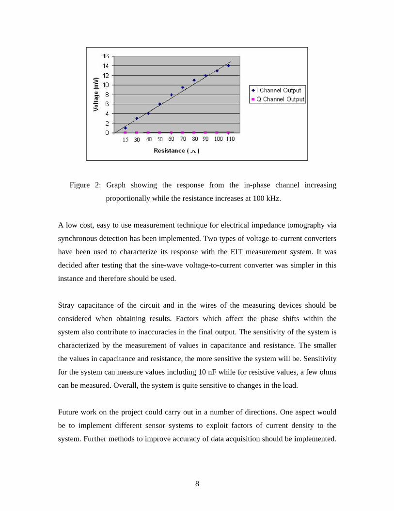
Measurements and readings were taken from the system created. The system was tested
for accuracy and sensitivity via a purely resistive and capacitive load. As shown in the
graph in figure 2 created by the results obtained, the in-phase channel increased
proportionally as the resistance increased. As for the quadrature channel, the
measurement in the imaginary channel increased as the value of capacitance decreased.
This was able to show the sensitivity of the system. Minor changes can be observed in the
quadrature channel while the load is purely resistive. This is caused by the inaccuracies
within the measurement system.
8
Figure 2: Graph showing the response from the in-phase channel increasing
proportionally while the resistance increases at 100 kHz.
A low cost, easy to use measurement technique for electrical impedance tomography via
synchronous detection has been implemented. Two types of voltage-to-current converters
have been used to characterize its response with the EIT measurement system. It was
decided after testing that the sine-wave voltage-to-current converter was simpler in this
instance and therefore should be used.
Stray capacitance of the circuit and in the wires of the measuring devices should be
considered when obtaining results. Factors which affect the phase shifts within the
system also contribute to inaccuracies in the final output. The sensitivity of the system is
characterized by the measurement of values in capacitance and resistance. The smaller
the values in capacitance and resistance, the more sensitive the system will be. Sensitivity
for the system can measure values including 10 nF while for resistive values, a few ohms
can be measured. Overall, the system is quite sensitive to changes in the load.
Future work on the project could carry out in a number of directions. One aspect would
be to implement different sensor systems to exploit factors of current density to the
system. Further methods to improve accuracy of data acquisition should be implemented.

9
Further research may also be done for the system by combining the existing system with
a multi-layered sensor design.
10
TABLE OF CONTENTS
Acknowledgements…………………………………………………………………….. i
Terms of Reference…………………………………………………………………….. ii
Synopsis………………………………………………………………………………... iii
Table of Contents………………………………………………………………………. viii
List of Illustrations…………………………………………………………………….. xii
CHAPTER 1: INTRODUCTION……………………………………………………. 1
1.1 Background to Process Tomography…………………………………………... 1
1.1.1Electrical Resistance Tomography (ERT)………………………………... 1
1.1.2 Electrical Capacitance Tomography (ECT)……………………………… 2
1.1.3Electrical Impedance Tomography (EIT)………………………………… 4
1.2 Problem Description…………………………………………………………… 5
1.3 Justification for the Research…………………………………………………... 6
1.4 Scope and Limitations…………………………………………………………. 6
1.5 Plan of Development……………………………………………………………7
CHAPTER 2: BRIEF OVERVIEW ON ELECTRICAL IMPEDANCE
TOMOGRAPHY ……………………………………………………. 8
2.1 Fundamentals of Electrical Impedance Tomography………………………….. 8
2.2 Fundamental Components of Electrical Impedance Tomography……………... 10
2.3 Sensor Hardware……………………………………………………………….. 14
2.4 Common Problems and Issues in Electrical Impedance Tomography………… 17
2.4.1 The Polarization Effect Which Occurs at the Electrodes………………… 17
2.4.2 Excitation Source Current………………………………………………... .18
2.4.3 Frequency of Operation………………………………………………….. 19
2.5 Data Acquisition……………………………………………………………….. 19

11
2.6 Measurements and Readings…………………………………………………... 20
CHAPTER 3: SENSING ELECTRONICS AND DESIGN……………………….. 23
3.1 Input Signal……………………………………………………………………. 23
3.2 Initial Designs………………………………………………………………….. 23
3.3 Input Source Current…………………………………………………………… 26
3.3.1 Initial Designs……………………………………………………………. 27
3.4 Sine-Wave Voltage-to-Current Converter……………………………………... 28
3.5 Square Wave Voltage-to-Current Converter…………………………………... 31
3.6 Measurement Techniques……………………………………………………… 34
3.7 Measurement Procedure……………………………………………………….. 36
3.8 Circuitry………………………………………………………………………... 38
3.8.1 AC Function Generator…………………………………………………... 38
3.8.2 Voltage-to-Current Conversion………………………………………….. 38
3.8.3 Demodulation and Filtering……………………………………………… 38
CHAPTER 4: EXPERIMENTAL PROTOCOL AND CIRCUITRY
BUILDING…………………………………………………………… 40
4.1 Synchronous Detection Circuitry……………………………………………… 40
4.2 Voltage to Current Converters…………………………………………………. 42
CHAPTER 5: ACTUAL TEST and RESULTS ……………………………………. 44
5.1 Test Results of a Purely Resistive Load under Test…………………………… 44
5.2 Test Results of a Purely Capacitive Load under Test…………………………. 45
5.3 Resistivity Profile of Tap Water with Electrode Plates………………………... 46
5.4 Resistivity Profile of Tap Water with a Different Arrangement of Electrodes... 47
5.5 Test Results of Fruits under Investigation……………………………………... 47
5.5.1 Potato…………………………………………………………………….. 48

12
5.5.2 Apple…………………………………………………………………….. 48
CHAPTER 6: INTERPRETATIONS AND DISCUSSIONS OF RESULTS…….. 49
6.1 An example of a measurement system………………………………………… 49
6.2 Measurement Techniques and Equipment Limitations………………………… 50
6.2.1 Probe-to-probe and Measurement Errors………………………………… 50
6.2.2 Circuit Board…………………………………………………………….. 51
6.2.3 Components……………………………………………………………… 51
6.3 Interpretation of the Purely Resistive and Capacitive Loads………………….. 52
6.4 Resistivity Profile of Tap Water………………………………………………. 56
6.5 Interpretations and Results of Fruit under Test………………………………… 58
6.6 Assessment of Current Source…………………………………………………. 60
6.6.1 Electrode…………………………………………………………………. 60
6.6.2 Current Density………………………………………………………….. 61
6.7 Limitations of Current Sensor…………………………………………………. 62
6.7.1 Sensitivity………………………………………………………………... 62
CHAPTER 7: CONCLUSIONS……………………………………………………... 63
CHAPTER 8: FUTURE WORK AND RECOMMENDATIONS………………… 65
8.1 The Role of Current Density…………………………………………………… 65
8.2 Different Types of Sensor Design…………………………………………….... 65
8.3 Recommendations……………………………………………………………… 66
LIST OF REFERENCES……………………………………………………………. 67
BIBLIOGRAPHY……………………………………………………………………. 70

13
APPENDIX A DATA SHEET OF ESCORT EFG-3210 FUNCTION
GENERATOR………………………………………………… 71
APPENDIX B DATA SHEET FOR THE OP-AMPS USED……………….. 73
APPENDIX C ADDITIONAL TEST RESULTS OF KNOWN
NETWORKS………………………………………………….. 77
APPENDIX D IMAGES OF ACTUAL MEASUREMENTS………………. 80
14
LIST OF ILLUSTRATIONS
FIGURES
Figure 1: Image showing the whole system with a device under test…………….. v
Figure 2: Graph showing the response from the in-phase channel increasing
proportionally while the resistance increases at 100 kHz………………. vi
Figure 1.1(a): Block diagram of a charge / discharge circuit………………………….. 3
Figure 1.1(b): Block diagram of an AC-based circuit…………………………………. 3
Figure 1.2: Diagram showing the electrical model of EIT………………………….. 4
Figure 2.1: Block diagram of the EIT system………………………………………. 10
Figure 2.2: Simple diagram showing the basic structure of a synchronous detection
system…………………………………………………………………… 12
Figure 2.3: Phasor diagram of output I and Q channels……………………………... 13
Figure 2.4: Electrical model of electrodes…………………………………………... 14
Figure 2.5: Current drive and the differential voltage measurement for the ‘4-
electrode’ configuration…………………………………………………. 15
Figure 2.6: Image showing the types of electrodes implemented in this research…... 16
Figure 2.7: A different type of electrode arrangement used for testing……………... 16
Figure 2.8: Figure showing the essential equipment of the system……………......... 20
Figure 2.9: Image of the vessel used for testing with electrodes for measurement
and tap water as the device under test…………………………………... 21
Figure 2.10: Image showing electrodes within a potato……………………………… 22
Figure 3.1: Diagram showing initial designs with the voltage driven source………. 23
Figure 3.2: Circuit diagram of initial designs with the current to voltage
converter………………………………………………………………… 24
Figure 3.3: Circuit showing demodulation and filtering of initial designs………….. 26
Figure 3.4: Circuit diagram of initial voltage-to-current converter…………………. 27
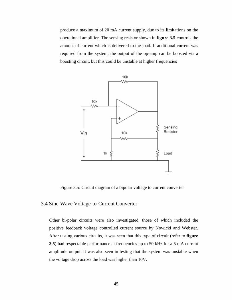
Figure 3.5: Circuit diagram of a bipolar voltage to current converter………………. 28

15
Figure 3.6: Circuit diagram of two op-amp VCCS with positive feedback…………. 29
Figure 3.7: Circuit diagram of sine-wave voltage-to-current converter……………... 30
Figure 3.8: Image of the measured waveform with cross-over distortion………….. 31
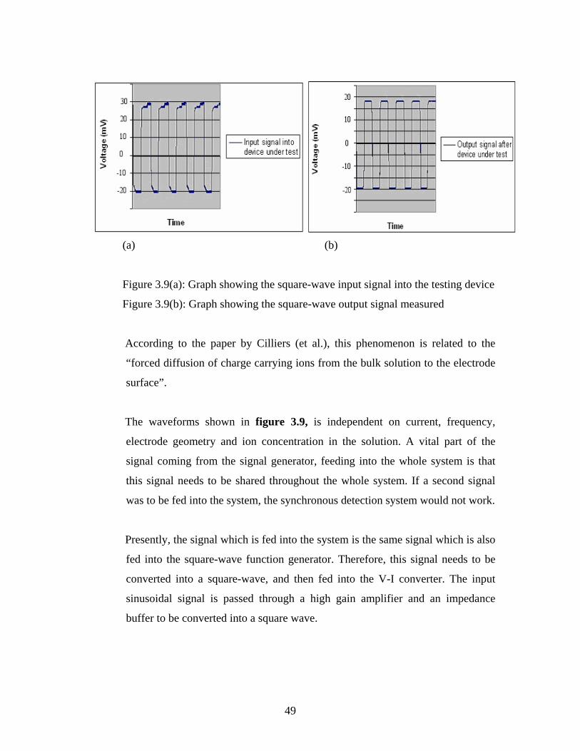
Figure 3.9(a): Graph showing the square-wave input signal into the testing device….. 32
Figure 3.9(b): Graph showing the square-wave output signal measured……………… 32
Figure 3.10: Circuit diagram of the square wave voltage-to-current converter which
was implemented………………………………………………………. 34
Figure 3.11: Diagram showing the current flow in the system……………………… 36
Figure 3.12: Flowchart showing the stages of the measurement procedure…………. 37
Figure 3.13: Diagram showing the final demodulation system implemented……….. 39
Figure 3.14: Circuit diagram of a 4th order Butterworth low pass filter……………... 39
Figure 4.1: Image showing the output waveform of the synchronous detector with
a resistive load…………………………………………………………. 40
Figure 4.2: Image of the output signal of the synchronous detector with a resistive
load…………………………………………………………………….. 41
Figure 4.3: Diagram showing one of the voltage reduction circuits……………….. 43
Figure 5.1: Graphs showing the chopped input signals to the synchronous detector
in the in-phase channel (a) and the quadrature channel (b)……………. 45
Figure 6.1: Image showing the whole measurement system……………………….. 49
Figure 6.2: Graph showing the resistivity profile of a resistive load at 10 kHz……. 52
Figure 6.3: Graph showing the resistivity profile of a resistive load at 100 kHz…... 53
Figure 6.4: Graph showing the profile of a capacitive load at 10 kHz……………... 54
Figure 6.5: Graph showing the profile of a capacitive load at 100 kHz……………. 55
Figure 6.6: Graph of the resistivity profile of water at varying frequencies with
electrode plates…………………………………………………………. 56
Figure 6.7: Graph of the resistivity profile of water at varying frequencies with the
designed electrodes…………………………………………………….. 57
Figure 6.8: Electrical model tap water as the device under test…………………..... 58
Figure 6.9(a): Graph showing the impedance of a potato through varying
frequencies……………………………………………………………... 58
16
Figure 6.9(b): Graph showing the impedance of an apple through varying
frequencies…………………………………………………................... 59
Figure 6.10(a):Graph of the output waveform from the V-I converter………………… 60
Figure 6.10(b):Graph of the input waveform injected into the device under test ……... 60
Figure 6.11: Diagram showing isopotential lines between electrode plates………… 61
Figure 7: Graph indicating the response of a known RC network to varying
frequency………………………………………………………………. 78
Figure 8: Graph showing the response of a different RC network to varying
frequencies……………………………………………………………... 79
Figure 9: Image taken of the input signal for a square-wave V-I converter with tap
water being tested……………………………………………………… 81
Figure 10: Image taken of the output signal for a square-wave V-I converter with tap
water being tested……………………………………………………… 81
Figure 11: Image taken of the output signal for a sine-wave V-I converter with tap
water being tested. …………………………………………………….. 81
Figure 12: Image taken of the input signal for a square-wave V-I converter for a
potato being tested……………………………………………………... 82
Figure 13: Image taken of the output signal for a square-wave V-I converter for a
potato being tested……………………………………………………... 82
Figure 14: Image taken of the output signal for a square-wave V-I converter with an
apple being tested……………………………………………………… 82
Figure 15: Image taken of the output signal for a sine-wave V-I converter by
implementing the designed electrode with tap water being tested…….. 83
Figure 16: Image taken of the synchronous detector output with a purely resistive
load…………………………………………………………………….. 83
Figure 17: Image taken of the synchronous detector output with a purely capacitive
load…………………………………………………………………….. 83

17
TABLES
Table 1: Table of results for a resistive load under testing………………………….. 44
Table 2: Table showing the measurement results of the quadrature channel……….. 46
Table 3: Table of values indicating the behavior of the measured impedance in tap
water through varying frequencies………………………………………… 46
Table 4: Table of measurements for tap water via a different arrangement of
electrodes………………………………………………………………….. 47
Table 5: Table indicating the behavior of a potato through varying frequencies…… 48
Table 6: Table indicating the behavior of an apple through varying frequencies…... 48
18
CHAPTER 1: INTRODUCTION
1.1 Background to Process Tomography
Process tomography has been around for a reasonable amount of time now. The
development of tomographic instrumentation, started in the 1950’s, and has led
to the widespread availability of body scanners which is part of modern medicine
nowadays [1]. Process tomography evolved essentially during the mid-1980. A
number of imaging equipment for processes was described in the 1970’s, but
generally this involved using ionization in x-rays, etc [1]. In the mid-1980’s
research started which led to the present work being done on process tomography
systems.
Tomography techniques are used to delineate the internal composition of pipes or
mixing vessels. There are many different types of tomographic methods used to
obtain different readings. For example, one of the types would be where sensors
(mainly electrodes) are mounted on a cylindrical vessel or object to obtain
different measurement readings through the device under test.
Various forms of tomography are being investigated around the world, of which
includes: Electrical Resistance Tomography, Electrical Capacitance Tomography,
and Electrical Impedance Tomography.
1.1.1 Electrical Resistance Tomography (ERT)
The fundamental aim of electrical resistance tomography is to establish the
electrical conductivity from measurements of voltage around the periphery
of a vessel. It is mainly used for measurement of gas-liquid and other mixed
liquids. ERT involves the acquisition of measurement signals
19
Electrical resistance tomography (ERT) is an accepted measuring technique
used in process engineering applications [4]. This type of technique is
known as one of the extremes of electrical impedance tomography.
Measurement of electrical resistance via four probes is widely used in a
range of applications. For example, resistance tomography measurements
with circular array electrodes were conducted in the biomedical and the
industrial fields. This is achieved by simply placing four equally-spaced
electrodes around a body, which are used for measurement purposes.
Electrical resistance tomography is an extension of this approach [6].
Usually a pair of electrodes is used as the initial driving pair. This pair of
electrodes would drive a sinusoidal current source, and the potential
difference would be measured between a separate pair of electrodes. This
specific arrangement reduces the contact impedance, although this factor is
less important in industrial applications compared to medical applications
[6].
1.1.2 Electrical Capacitance Tomography (ECT)
Electrical capacitance tomography is known as the other extreme of
electrical impedance tomography, whereby it is the measurement of the
dielectric constant. This was one of the techniques which were first
developed for process tomography. It is low cost, high speed, robust and
non-intrusive. As shown in the equation below, the area of the plate is
known, as well as the distance between them, so effectively by measuring
the capacitance; we are effectively measuring the dielectric constant.
ACdε
=
A – Area of plate
20
d – Distance between plates
ε - Dielectric constant
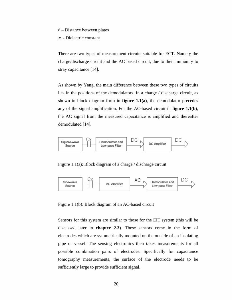
There are two types of measurement circuits suitable for ECT. Namely the
charge/discharge circuit and the AC based circuit, due to their immunity to
stray capacitance [14].
As shown by Yang, the main difference between these two types of circuits
lies in the positions of the demodulators. In a charge / discharge circuit, as
shown in block diagram form in figure 1.1(a), the demodulator precedes
any of the signal amplification. For the AC-based circuit in figure 1.1(b),
the AC signal from the measured capacitance is amplified and thereafter
demodulated [14].
Figure 1.1(a): Block diagram of a charge / discharge circuit
Figure 1.1(b): Block diagram of an AC-based circuit
Sensors for this system are similar to those for the EIT system (this will be
discussed later in chapter 2.3). These sensors come in the form of
electrodes which are symmetrically mounted on the outside of an insulating
pipe or vessel. The sensing electronics then takes measurements for all
possible combination pairs of electrodes. Specifically for capacitance
tomography measurements, the surface of the electrode needs to be
sufficiently large to provide sufficient signal.
21
1.1.3 Electrical Impedance Tomography (EIT)
Electrical impedance tomography (also called applied potential tomography)
is a non-invasive inverse method which is able to determine the electrical
conductivity of a medium by making voltage and current measurements at
the boundaries of the object.
This special technique is widely used in the medical and the industrial field.
In industry, it is mainly used to recreate images of the contents within a pipe,
vessel or object. This helps the operator to visualize the internal behavior of
industrial processes. There are various applications whereby impedance
tomography is used in medical imaging and measurement purposes [17].
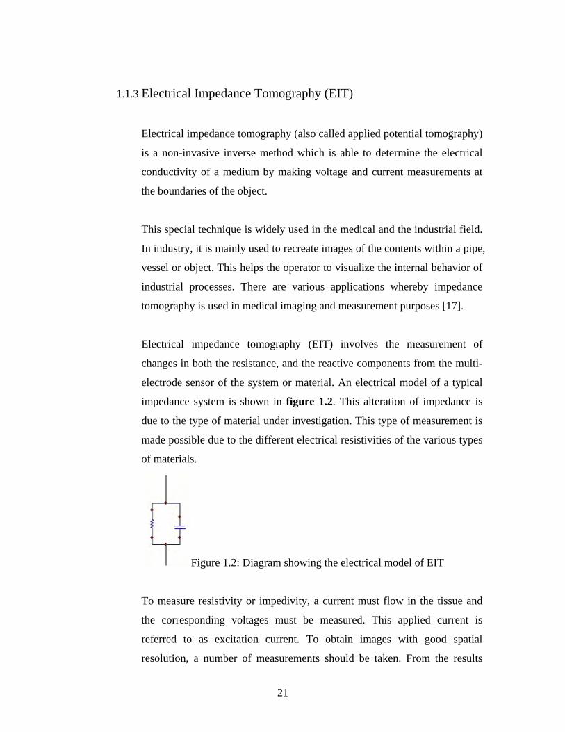
Electrical impedance tomography (EIT) involves the measurement of
changes in both the resistance, and the reactive components from the multi-
electrode sensor of the system or material. An electrical model of a typical
impedance system is shown in figure 1.2. This alteration of impedance is
due to the type of material under investigation. This type of measurement is
made possible due to the different electrical resistivities of the various types
of materials.
Figure 1.2: Diagram showing the electrical model of EIT
To measure resistivity or impedivity, a current must flow in the tissue and
the corresponding voltages must be measured. This applied current is
referred to as excitation current. To obtain images with good spatial
resolution, a number of measurements should be taken. From the results
22
obtained, an image reconstruction technique is developed to generate the
tomographic image [8].
There is a variety of methods for tomography sensing within mineral
separation. Various other electrical techniques for chemical processes within
industry are also available.
Previous developments on electrical impedance tomography were done for
imaging vessels which contained electrically conducting fluids. In other
work, medical EIT progressed because some of the instrumentation
problems were common to medical and to process tomography. However,
there are still major differences in the usage for medical and industrial
purposes. In medical applications, they are used to measure the location of
objects in space, while in industry, both location and velocity of movement
needs to be measured [1].
1.2 Problem Description
Within industry nowadays, various pipes or vessels are used in processes, and it
is difficult to see what is within them. Therefore, a system has to be developed
whereby the controller is able to view objects within these pipes or vessels
without actually having to tamper with them.
The way around this problem would be to place sensing electronics around the
actual pipe or vessel. Via these sensing electronics, we are able to take
measurements and recreate an image of what is contained within.
Electronics of this nature needs to be created such that it is affordable and easy to
operate. A voltage-to-current converter is used to inject the input current source,
while other pairs of electrodes are able to pick this up and convert this signal into
a voltage measurement. Various types of voltage-to-current converters need to be
23
built, implemented and tested for suitability and sensitivity. Thereafter, a
synchronous detection systems needs to be tested together with the voltage-to-
current converter via the sensing electrodes.
1.3 Justification for the Research
The objectives of this thesis are to create and test a synchronous detection system
for an electrical impedance tomography system. An AC signal of 1 kHz to 100
kHz is generated and injected into the object under test. This input current source
can be from one of the following two types. It can either be a sine-wave V-I
converter or a square-wave V-I converter.
The output voltage signal is measured between a pair of electrodes and will be
phase shifted. The synchronous detection system should measure the phase and
amplitude at the output (via the real and imaginary parts of the measurement).
After the measurements have been taken, plots will be made from the readings,
and an electrical model of the object being tested can be created.
1.4 Scope and Limitations
There are various types of systems used for process tomography. This project is
set on creating and designing systems which are economical, simple and
affordable. Therefore the only limitations are the components which form part of
the circuit design.
Certain limitations for this research are designs for the synchronous detectors and
voltage-to-current converters which operate at high frequencies. If proper
precautions are not taken at higher frequencies, distortions and large phase shifts
will start to occur within these components, and therefore cause inaccurate
measurements.
24
1.5 Plan of Development
The theory behind electrical impedance tomography needs to be investigated first
of all. Thereafter, various circuit designs needs to be investigated to assess the
appropriate designs for this specific system.
Two types of voltage-to-current converters needs to be created to operate at
frequencies of 1 kHz to 100 kHz. A synchronous detection system needs to be
created with two channel outputs for measurements between two pairs of
electrodes.
The acquired data needs to be evaluated and processed for impedance
measurements of various objects. A profile of the various objects tested needs to
be created and discussed.
25
CHAPTER 2: BRIEF OVERVIEW ON ELECTRICAL IMPEDANCE
TOMOGRAPHY
Electrical impedance tomography allows one to measure the impedance, or its inverse,
the admittance to gain information about the object. Usually electrodes are placed along
the boundary of the object ensuring that they come into contact with the object being
measured. An image of the object can be recreated from the measurements obtained. This
allows the user to visualize the object without having to enter the medium.
2.1 Fundamentals of Electrical Impedance Tomography
To be able to recreate tomographic images of objects enables us to unravel the
complexities of different structures without having to invade the object.
Measurements for tomography are non-intrusive, can be thought of as
“penetrating the wall” but without actually having to enter the medium under
investigation [17].
Process tomography is needed to improve the design of processes handling multi-
component mixtures by enabling boundaries between different components in a
process to be imaged in real-time using non-intrusive sensors [1].
Various achievements have been made in tomography, especially in the medical
field. Identification of tumors, particularly using x-rays as a source of energy, are
some of the achievements made. More recently, achievements were made by
using magnetic resonance and electrical excitation [11]. Tomography is therefore
extremely complex, involving target regions with multiple sensor electronics,
data acquisition and data inversion [17].
26
There are various tomographic imaging techniques which can be used, to name
some of them, there are: electrical resistance tomography, electrical capacitance
tomography, and electrical impedance tomography. The one that the author is
investigating is electrical impedance tomography.
As discussed in chapter 1, electrical impedance tomography is a non-invasive
method which is able to determine the electrical conductivity of a medium by
making voltage and current measurements at the boundaries of the object. This
specific technique of imaging minerals and other materials is used in industry but
at a cost. Further research is being conducted in this field to create a more simple
and low cost method of imaging these objects.
Their advantages are that it is inexpensive, portable, safe, and it produces images
many times per second. Other advantages are that the measurement of electrical
conductivity gives direct information of the conductivity of the medium being
tested.
The main difference between the various different types of systems that have been
discussed is the type of current source that is used. There are mainly two types of
current sources which are provided; the square-wave (charge / discharge) and the
sinusoidal pulse excitation source (refer to chapter 3.4). Different types of
excitation sources have different effects on the system as a whole and also on the
measuring electrodes.
Within electrical impedance tomography, a current source is injected into the
device under test via a pair of electrodes, while another pair of electrodes
measures the potential difference. By injecting current through the electrodes, the
current density, and hence the sensitivity near the centre of the vessel can be
increased [8]. The input signal through the electrode is kept constant at all times
(this includes the positive and negative half cycles). The voltage measurement is
picked up via a differential amplifier.
27
The sensitivity of the electrical impedance tomography system depends entirely
on the current density inside the object. In areas where the sensitivity is low, the
changes in resistivity might not cause detectable changes in voltages which are
measured via the electrodes [8]. In classical electrical impedance tomography
systems, electrodes attached to the surface of the object is used.
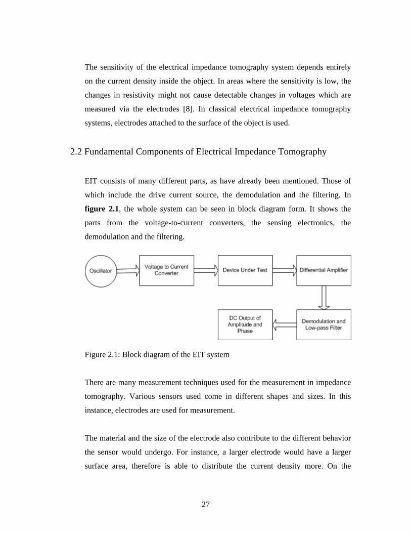
2.2 Fundamental Components of Electrical Impedance Tomography
EIT consists of many different parts, as have already been mentioned. Those of
which include the drive current source, the demodulation and the filtering. In
figure 2.1, the whole system can be seen in block diagram form. It shows the
parts from the voltage-to-current converters, the sensing electronics, the
demodulation and the filtering.
Figure 2.1: Block diagram of the EIT system
There are many measurement techniques used for the measurement in impedance
tomography. Various sensors used come in different shapes and sizes. In this
instance, electrodes are used for measurement.
The material and the size of the electrode also contribute to the different behavior
the sensor would undergo. For instance, a larger electrode would have a larger
surface area, therefore is able to distribute the current density more. On the
28
sensing side, smaller electrodes would be used to achieve better results, by
eliminating the unwanted noisy signals.
Circuitry for electrical impedance tomography consists of the input current source
and the synchronous detection circuit (for demodulation). Various designs are
available for circuits in synchronous detection and voltage-to-current converters,
but investigation into all these designs are necessary to asses the most suitable one.
Each aspect / sub-sections involved in the system is critical. The current injected
is a constant current source, while the sensors, the electrodes, are vital in the
measurement process, as shown in section 2.3.
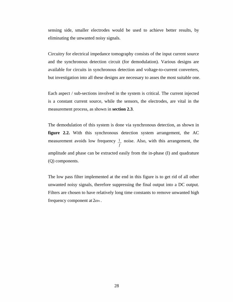
The demodulation of this system is done via synchronous detection, as shown in
figure 2.2. With this synchronous detection system arrangement, the AC
measurement avoids low frequency 1f
noise. Also, with this arrangement, the
amplitude and phase can be extracted easily from the in-phase (I) and quadrature
(Q) components.
The low pass filter implemented at the end in this figure is to get rid of all other
unwanted noisy signals, therefore suppressing the final output into a DC output.
Filters are chosen to have relatively long time constants to remove unwanted high
frequency component at 02ω .
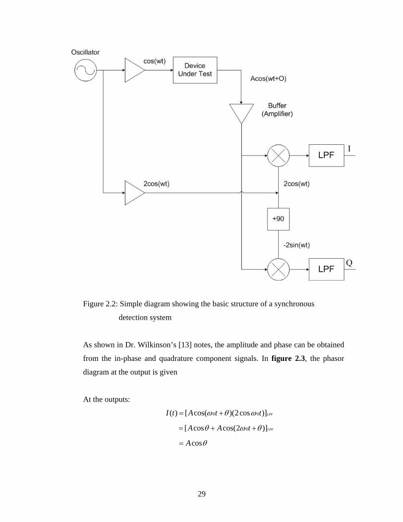
29
Figure 2.2: Simple diagram showing the basic structure of a synchronous
detection system
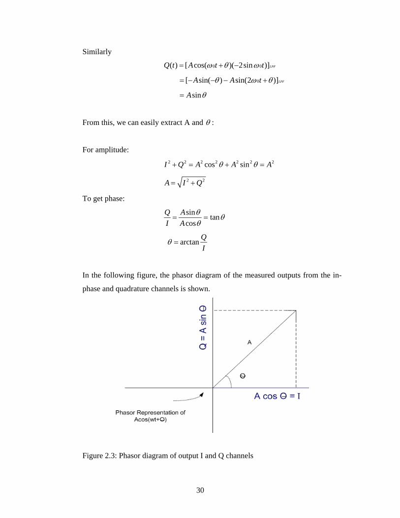
As shown in Dr. Wilkinson’s [13] notes, the amplitude and phase can be obtained
from the in-phase and quadrature component signals. In figure 2.3, the phasor
diagram at the output is given
At the outputs:
0 0( ) [ cos( )(2cos )]LPFI t A t tω θ ω= +
0[ cos cos(2 )]LPFA A tθ ω θ= + +
cosA θ=
30
Similarly
0 0( ) [ cos( )( 2sin )]LPFQ t A t tω θ ω= + −
0[ sin( ) sin(2 )]LPFA A tθ ω θ= − − − +
sinA θ=
From this, we can easily extract A and θ :
For amplitude:
2 2 2 2 2 2 2cos sinI Q A A Aθ θ+ = + =
2 2A I Q= +
To get phase:
sin tancos
Q AI A
θ θθ
= =
arctan QI
θ =
In the following figure, the phasor diagram of the measured outputs from the in-
phase and quadrature channels is shown.
Figure 2.3: Phasor diagram of output I and Q channels
31
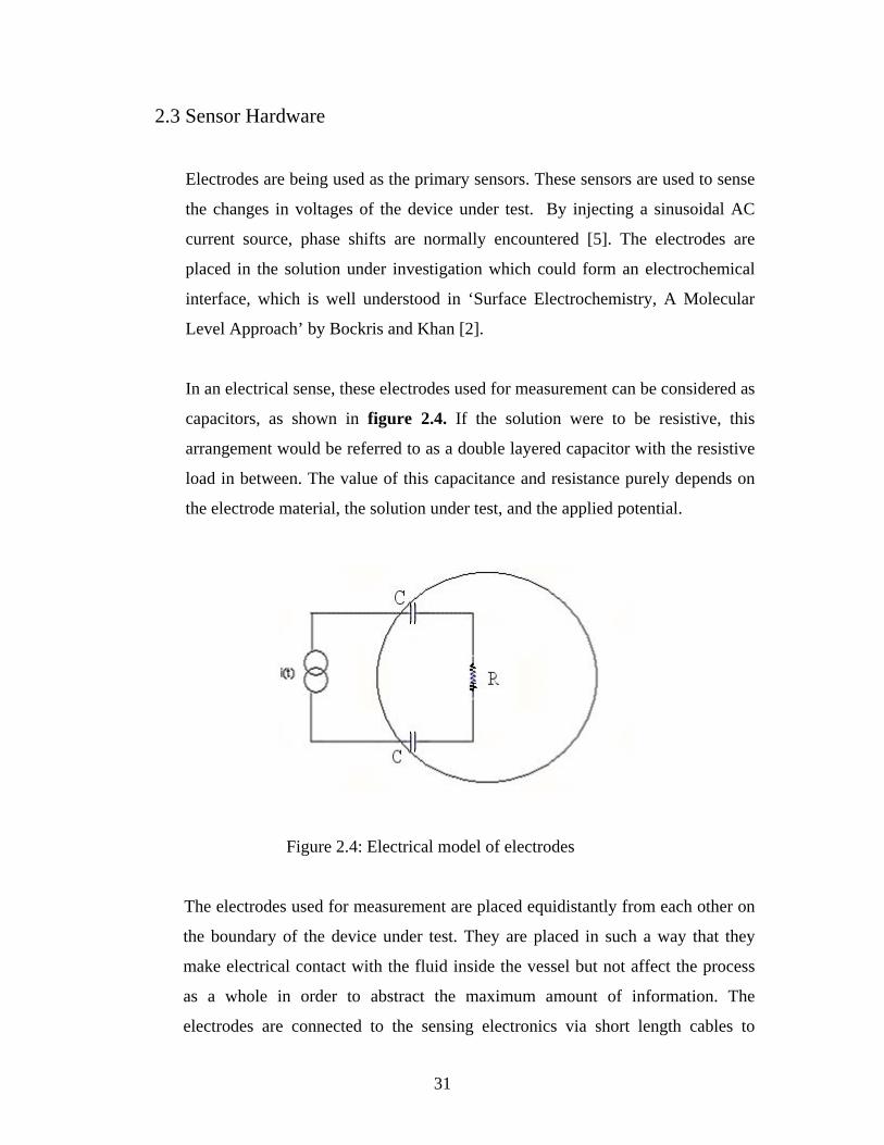
2.3 Sensor Hardware
Electrodes are being used as the primary sensors. These sensors are used to sense
the changes in voltages of the device under test. By injecting a sinusoidal AC
current source, phase shifts are normally encountered [5]. The electrodes are
placed in the solution under investigation which could form an electrochemical
interface, which is well understood in ‘Surface Electrochemistry, A Molecular
Level Approach’ by Bockris and Khan [2].
In an electrical sense, these electrodes used for measurement can be considered as
capacitors, as shown in figure 2.4. If the solution were to be resistive, this
arrangement would be referred to as a double layered capacitor with the resistive
load in between. The value of this capacitance and resistance purely depends on
the electrode material, the solution under test, and the applied potential.
Figure 2.4: Electrical model of electrodes
The electrodes used for measurement are placed equidistantly from each other on
the boundary of the device under test. They are placed in such a way that they
make electrical contact with the fluid inside the vessel but not affect the process
as a whole in order to abstract the maximum amount of information. The
electrodes are connected to the sensing electronics via short length cables to
32
reduce the amount of noise and interference. Stray capacitance and larger noise
interference normally arise from larger lengths of cable.
The material that the electrodes are made of depends on the type of corrosive /
abrasive nature of the substance under testing. Typically, the type of materials the
electrodes are made of are: brass / copper, stainless steel or silver palladium alloy
which is commercially available.
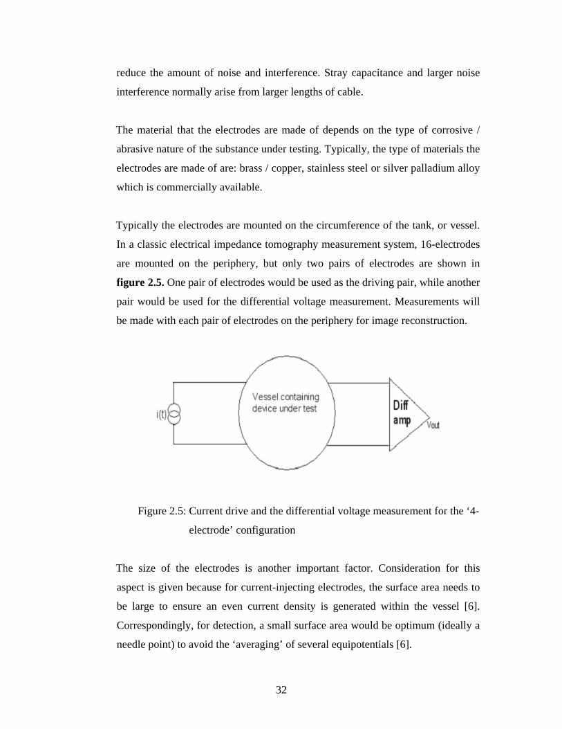
Typically the electrodes are mounted on the circumference of the tank, or vessel.
In a classic electrical impedance tomography measurement system, 16-electrodes
are mounted on the periphery, but only two pairs of electrodes are shown in
figure 2.5. One pair of electrodes would be used as the driving pair, while another
pair would be used for the differential voltage measurement. Measurements will
be made with each pair of electrodes on the periphery for image reconstruction.
Figure 2.5: Current drive and the differential voltage measurement for the ‘4-
electrode’ configuration
The size of the electrodes is another important factor. Consideration for this
aspect is given because for current-injecting electrodes, the surface area needs to
be large to ensure an even current density is generated within the vessel [6].
Correspondingly, for detection, a small surface area would be optimum (ideally a
needle point) to avoid the ‘averaging’ of several equipotentials [6].
33
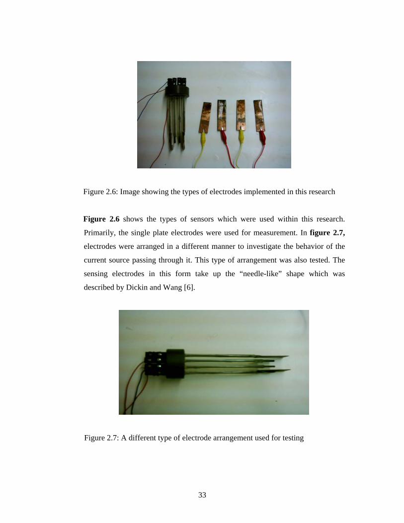
Figure 2.6: Image showing the types of electrodes implemented in this research
Figure 2.6 shows the types of sensors which were used within this research.
Primarily, the single plate electrodes were used for measurement. In figure 2.7,
electrodes were arranged in a different manner to investigate the behavior of the
current source passing through it. This type of arrangement was also tested. The
sensing electrodes in this form take up the “needle-like” shape which was
described by Dickin and Wang [6].
Figure 2.7: A different type of electrode arrangement used for testing
34
2.4 Common Problems and Issues in Electrical Impedance Tomography
There were various issues involved in electrical impedance tomography. Areas
where they were likely to occur were at the electrodes, i.e. the polarization effects.
The excitation source was another area of concern. By implementing the wrong
type of current source, or the distribution of current density was uneven,
measurements on the sensing side would be inaccurate.
Frequency of operation should also be considered, since the type of circuitry
implemented and the components used had their limitations. At larger and
undesirable frequencies, distortions started to occur, causing unwanted noise, and
inaccurate readings.
2.4.1 The Polarization Effect Which Occurs at the Electrodes
Initially, the research started out by implementing a voltage driven source
through a pair of electrodes. Various aspects of this method had to be
researched and experimented in order to understand the different effects.
By injecting a voltage source, electrochemical effects would occur at the
electrodes. The current to voltage conversion thereafter was also quite
tedious, as shown later in chapter 3.2.
By using a current driven system, the current distribution within the
medium under test is independent of the electrochemical effects which
would occur between the driving electrodes and the solution [4]. At the
same time, a bi-directional current was used, which would eliminate the
long-term polarization effects which would occur at the electrodes.
As a result of the forced current, various reactions may occur at the drive
electrodes depending on the complexities of the substance being tested. In
35
the investigation whereby the device under test is tap water, and at the
voltage levels used, the reactions which were likely to occur would be the
electrolysis of water.
2.4.2 Excitation Source Current
A bi-directional pulsed DC current source was implemented for this
research. This current source was driven via a pair of electrodes and was
kept constant during each half cycle. For the square-wave V-I converter,
the driving waveform would be a square wave. The potential difference
measured via another pair of electrodes through a high impedance
differential amplifier is also constant through every half cycle, and
therefore is also a square wave,
After implementing the voltage-to-current converters, various other
filtering and amplifiers needed to be added. Typically for the square-wave
voltage-to-current converter, by injecting a square-wave current source,
the measured output resulted in a square-wave as well. This square-wave
had to be converted into a sine-wave in order to pass it through the
demodulation system. Filtering needed to be done at the harmonics of the
square-wave in order to smooth it out into a sine-wave (refer to chapter
3.5 for circuit diagrams).
For a sine-wave current source, it would not be as complicated as
implementing the square-wave current to voltage converter. By using the
sine-wave current source, the differential voltage measured at the
receiving end would also be a sine-wave (or a slightly distorted one). If
slight distortions occur, this can be resolved by implementing filters to
smooth the signal out, but one must be weary of phase shifts.
36
The disadvantage of using this particular design to create a sine-wave
voltage-to-current converter is that crossover distortions occur. These
distortions are caused by the switching times of the transistors (for more
details and discussions, refer to chapter 3.4).
2.4.3 Frequency of Operation
Initial experiments have been made in the biomedical field whereby
frequencies with bandwidths of 75 Hz – 153 kHz have been injected.
Usually the input current is limited to less than 5 mA amplitude, and over
20 kHz frequency are used to prevent discomfort within the patient [6].
Depending on the type of process, but for slower changing processes,
more accurate measurements are achieved at lower frequencies.
The proposed range of frequencies for this research was from 1 kHz – 100
kHz. Since better and more sophisticated components are being developed
(but still maintaining a low cost budget), frequency of operation has been
achieved up to 300 kHz in the square-wave voltage-to-current converter. It
is possible to operate at even higher frequencies, but components would be
more expensive and even more complex to build and to operate. For the
sine-wave voltage-to-current converter, frequency ranges of up to 300 kHz
have been achieved (with some crossover distortion, which is
unavoidable).
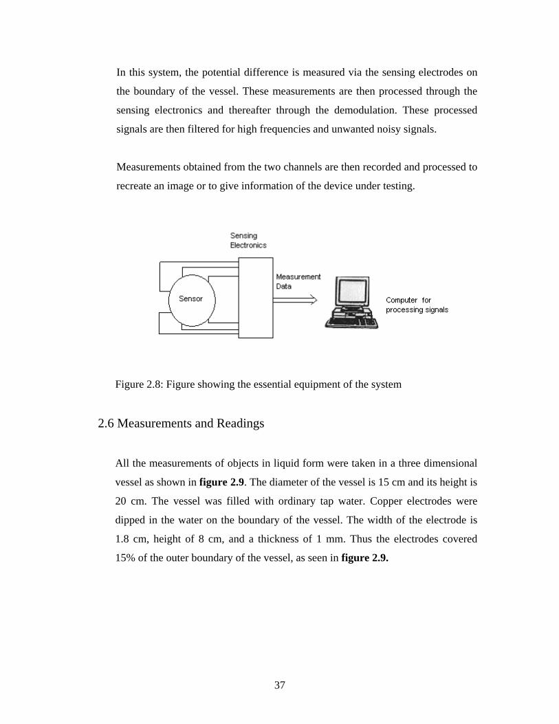
2.5 Data Acquisition
The primary aim of designing an EIT system is to measure the distribution of the
electrically conductive medium within an object. Figure 2.8 shows the schematic
diagram of the EIT measurement system implemented.
37
In this system, the potential difference is measured via the sensing electrodes on
the boundary of the vessel. These measurements are then processed through the
sensing electronics and thereafter through the demodulation. These processed
signals are then filtered for high frequencies and unwanted noisy signals.
Measurements obtained from the two channels are then recorded and processed to
recreate an image or to give information of the device under testing.
Figure 2.8: Figure showing the essential equipment of the system
2.6 Measurements and Readings
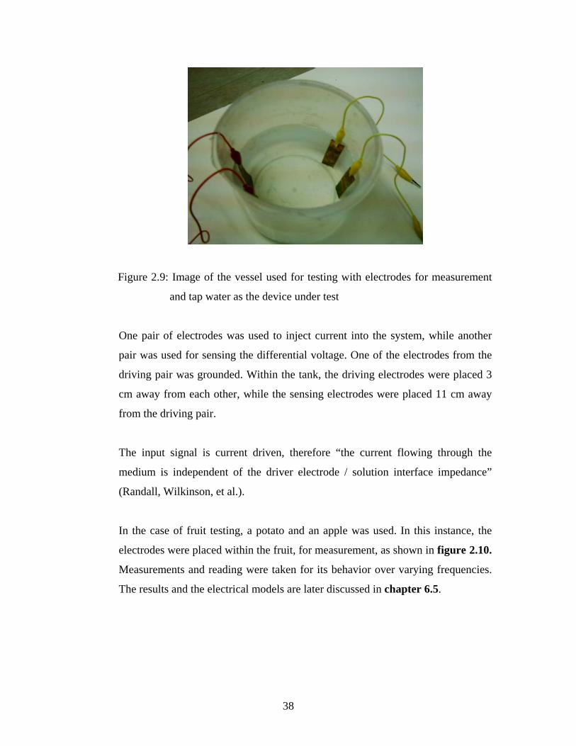
All the measurements of objects in liquid form were taken in a three dimensional
vessel as shown in figure 2.9. The diameter of the vessel is 15 cm and its height is
20 cm. The vessel was filled with ordinary tap water. Copper electrodes were
dipped in the water on the boundary of the vessel. The width of the electrode is
1.8 cm, height of 8 cm, and a thickness of 1 mm. Thus the electrodes covered
15% of the outer boundary of the vessel, as seen in figure 2.9.
38
Figure 2.9: Image of the vessel used for testing with electrodes for measurement
and tap water as the device under test
One pair of electrodes was used to inject current into the system, while another
pair was used for sensing the differential voltage. One of the electrodes from the
driving pair was grounded. Within the tank, the driving electrodes were placed 3
cm away from each other, while the sensing electrodes were placed 11 cm away
from the driving pair.
The input signal is current driven, therefore “the current flowing through the
medium is independent of the driver electrode / solution interface impedance”
(Randall, Wilkinson, et al.).
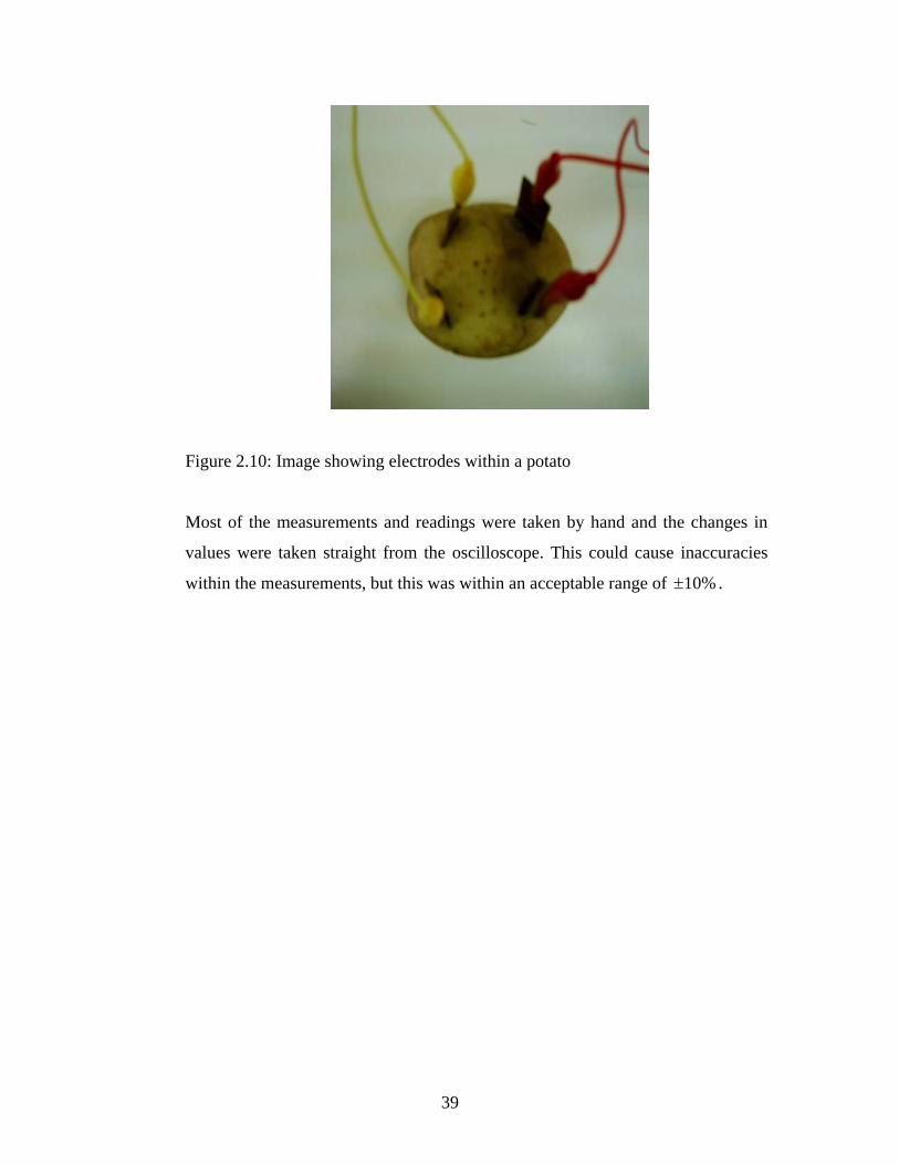
In the case of fruit testing, a potato and an apple was used. In this instance, the
electrodes were placed within the fruit, for measurement, as shown in figure 2.10.
Measurements and reading were taken for its behavior over varying frequencies.
The results and the electrical models are later discussed in chapter 6.5.
39
Figure 2.10: Image showing electrodes within a potato
Most of the measurements and readings were taken by hand and the changes in
values were taken straight from the oscilloscope. This could cause inaccuracies
within the measurements, but this was within an acceptable range of 10%± .
40
CHAPTER 3: SENSING ELECTRONICS AND DESIGN
The measurement system created for impedance measurements consisted of the sensing,
demodulation, and filtering electronics. The most complex part in these designs was the
demodulation, whereby a synchronous detector was used. In this chapter, designs which
were initially implemented, and the modified implemented designs will be discussed.
Designs and circuit diagrams for the voltage-to-current converters implemented will also
be discussed here.
3.1 Input Signal
The input AC signal is driven from the Escort EFG-3210 function generator.
Aspects and details of this device can be found in Appendix A.
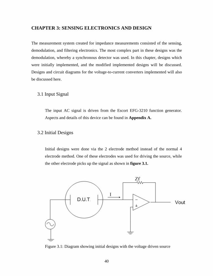
3.2 Initial Designs
Initial designs were done via the 2 electrode method instead of the normal 4
electrode method. One of these electrodes was used for driving the source, while
the other electrode picks up the signal as shown in figure 3.1.
Figure 3.1: Diagram showing initial designs with the voltage driven source
41
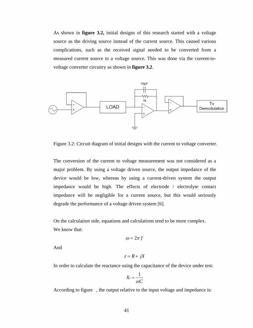
As shown in figure 3.2, initial designs of this research started with a voltage
source as the driving source instead of the current source. This caused various
complications, such as the received signal needed to be converted from a
measured current source to a voltage source. This was done via the current-to-
voltage converter circuitry as shown in figure 3.2.
Figure 3.2: Circuit diagram of initial designs with the current to voltage converter.
The conversion of the current to voltage measurement was not considered as a
major problem. By using a voltage driven source, the output impedance of the
device would be low, whereas by using a current-driven system the output
impedance would be high. The effects of electrode / electrolyte contact
impedance will be negligible for a current source, but this would seriously
degrade the performance of a voltage driven system [6].
On the calculation side, equations and calculations tend to be more complex.
We know that:
2 fω π=
And
z R jX= +
In order to calculate the reactance using the capacitance of the device under test:
1cX
Cω=
According to figure , the output relative to the input voltage and impedance is:
42
( ) ( )( ) ( )
o f
i
V ZV Z
ω ωω ω
= −
( )( ) ( )( )
fo i
ZV VZωω ωω
∴ = −
As can be seen from the above equations, ( )fZ ω is known, ( )iV ω is of constant
amplitude, while ( )Z ω is the device under test. Therefore
1( )( )
oVZ
ω αω
Since
1 ( )( )
YZ
ωω
=
( )Y G jbω = +
1R jXG jb
+ =+
As shown, with this initial method, the inverse of the actual impedance needed is
calculated. Although this is not a huge problem, but it makes the mathematics
troublesome which could cause complications for future reconstruction and
calculations.
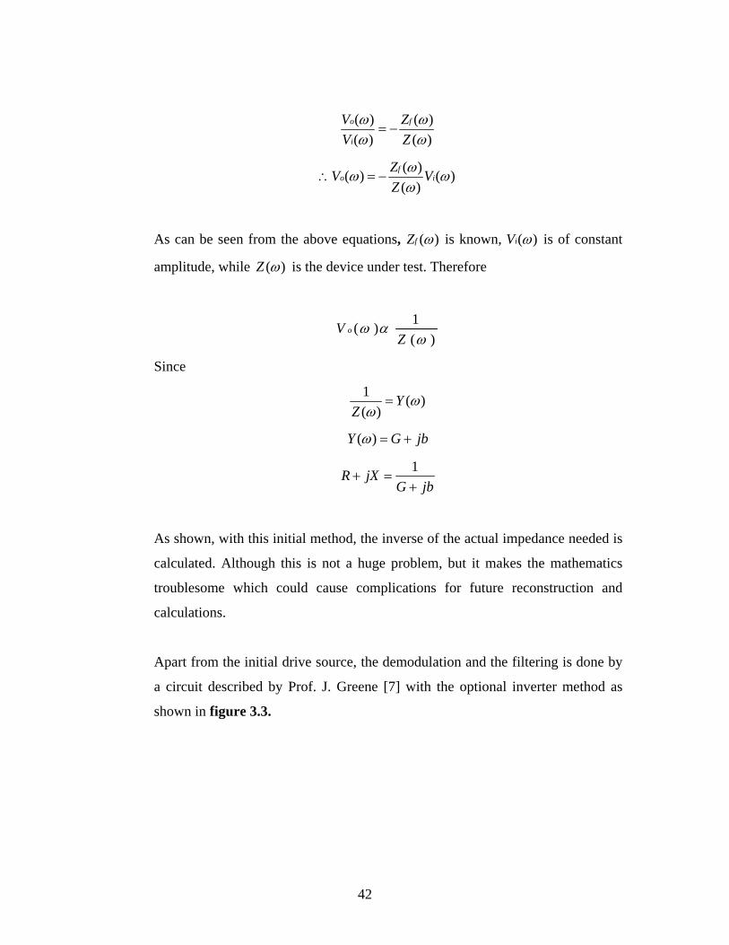
Apart from the initial drive source, the demodulation and the filtering is done by
a circuit described by Prof. J. Greene [7] with the optional inverter method as
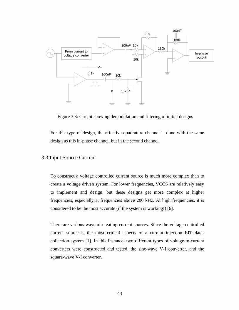
shown in figure 3.3.
43
From current tovoltage converter In-phase
output
V+
1k 100nF 10k
10k
100nF 10k
10k
10k
160k
160k
100nF
Figure 3.3: Circuit showing demodulation and filtering of initial designs
For this type of design, the effective quadrature channel is done with the same
design as this in-phase channel, but in the second channel.
3.3 Input Source Current
To construct a voltage controlled current source is much more complex than to
create a voltage driven system. For lower frequencies, VCCS are relatively easy
to implement and design, but these designs get more complex at higher
frequencies, especially at frequencies above 200 kHz. At high frequencies, it is
considered to be the most accurate (if the system is working!) [6].
There are various ways of creating current sources. Since the voltage controlled
current source is the most critical aspects of a current injection EIT data-
collection system [1]. In this instance, two different types of voltage-to-current
converters were constructed and tested, the sine-wave V-I converter, and the
square-wave V-I converter.
44
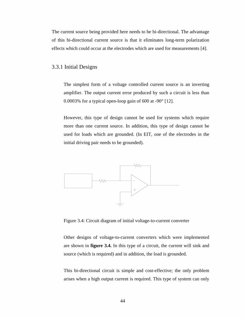
The current source being provided here needs to be bi-directional. The advantage
of this bi-directional current source is that it eliminates long-term polarization
effects which could occur at the electrodes which are used for measurements [4].
3.3.1 Initial Designs
The simplest form of a voltage controlled current source is an inverting
amplifier. The output current error produced by such a circuit is less than
0.0003% for a typical open-loop gain of 600 at -90° [12].
However, this type of design cannot be used for systems which require
more than one current source. In addition, this type of design cannot be
used for loads which are grounded. (In EIT, one of the electrodes in the
initial driving pair needs to be grounded).
Figure 3.4: Circuit diagram of initial voltage-to-current converter
Other designs of voltage-to-current converters which were implemented
are shown in figure 3.4. In this type of a circuit, the current will sink and
source (which is required) and in addition, the load is grounded.
This bi-directional circuit is simple and cost-effective; the only problem
arises when a high output current is required. This type of system can only
45
produce a maximum of 20 mA current supply, due to its limitations on the
operational amplifier. The sensing resistor shown in figure 3.5 controls the
amount of current which is delivered to the load. If additional current was
required from the system, the output of the op-amp can be boosted via a
boosting circuit, but this could be unstable at higher frequencies
Figure 3.5: Circuit diagram of a bipolar voltage to current converter
3.4 Sine-Wave Voltage-to-Current Converter
Other bi-polar circuits were also investigated, those of which included the
positive feedback voltage controlled current source by Nowicki and Webster.
After testing various circuits, it was seen that this type of circuit (refer to figure
3.5) had respectable performance at frequencies up to 50 kHz for a 5 mA current
amplitude output. It was also seen in testing that the system was unstable when
the voltage drop across the load was higher than 10V.
46
Other various systems of voltage-to-current converters were also investigated
such as the ones developed by Lidgey and Zhu [10]. Systems of that nature are
difficult to modify for higher frequencies and high speeds.
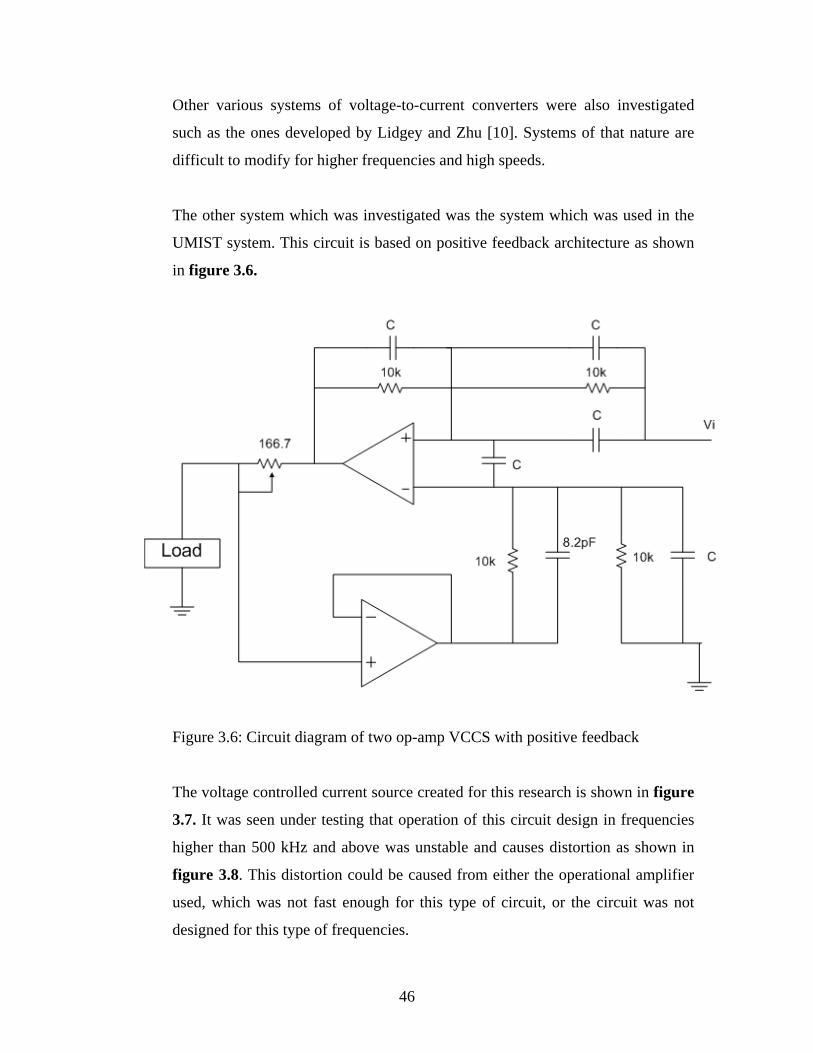
The other system which was investigated was the system which was used in the
UMIST system. This circuit is based on positive feedback architecture as shown
in figure 3.6.
Figure 3.6: Circuit diagram of two op-amp VCCS with positive feedback
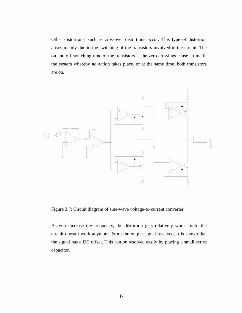
The voltage controlled current source created for this research is shown in figure
3.7. It was seen under testing that operation of this circuit design in frequencies
higher than 500 kHz and above was unstable and causes distortion as shown in
figure 3.8. This distortion could be caused from either the operational amplifier
used, which was not fast enough for this type of circuit, or the circuit was not
designed for this type of frequencies.
47
Other distortions, such as crossover distortions occur. This type of distortion
arises mainly due to the switching of the transistors involved in the circuit. The
on and off switching time of the transistors at the zero crossings cause a time in
the system whereby no action takes place, or at the same time, both transistors
are on.
Figure 3.7: Circuit diagram of sine-wave voltage-to-current converter
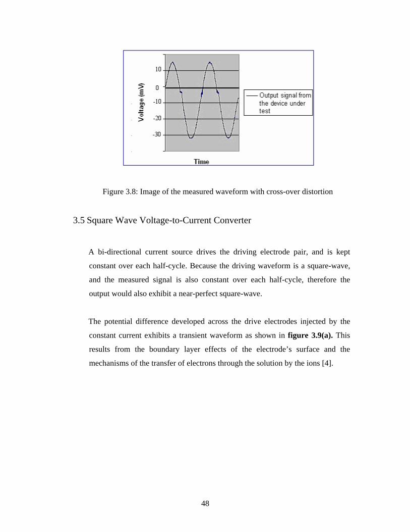
As you increase the frequency, the distortion gets relatively worse, until the
circuit doesn’t work anymore. From the output signal received, it is shown that
the signal has a DC offset. This can be resolved easily by placing a small series
capacitor.
48
Figure 3.8: Image of the measured waveform with cross-over distortion
3.5 Square Wave Voltage-to-Current Converter
A bi-directional current source drives the driving electrode pair, and is kept
constant over each half-cycle. Because the driving waveform is a square-wave,
and the measured signal is also constant over each half-cycle, therefore the
output would also exhibit a near-perfect square-wave.
The potential difference developed across the drive electrodes injected by the
constant current exhibits a transient waveform as shown in figure 3.9(a). This
results from the boundary layer effects of the electrode’s surface and the
mechanisms of the transfer of electrons through the solution by the ions [4].
49
(a) (b)
Figure 3.9(a): Graph showing the square-wave input signal into the testing device
Figure 3.9(b): Graph showing the square-wave output signal measured
According to the paper by Cilliers (et al.), this phenomenon is related to the
“forced diffusion of charge carrying ions from the bulk solution to the electrode
surface”.
The waveforms shown in figure 3.9, is independent on current, frequency,
electrode geometry and ion concentration in the solution. A vital part of the
signal coming from the signal generator, feeding into the whole system is that
this signal needs to be shared throughout the whole system. If a second signal
was to be fed into the system, the synchronous detection system would not work.
Presently, the signal which is fed into the system is the same signal which is also
fed into the square-wave function generator. Therefore, this signal needs to be
converted into a square-wave, and then fed into the V-I converter. The input
sinusoidal signal is passed through a high gain amplifier and an impedance
buffer to be converted into a square wave.
50
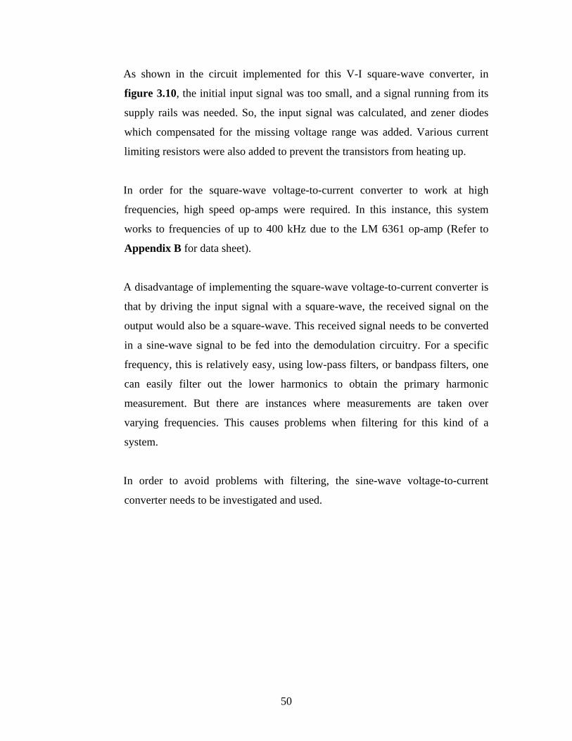
As shown in the circuit implemented for this V-I square-wave converter, in
figure 3.10, the initial input signal was too small, and a signal running from its
supply rails was needed. So, the input signal was calculated, and zener diodes
which compensated for the missing voltage range was added. Various current
limiting resistors were also added to prevent the transistors from heating up.
In order for the square-wave voltage-to-current converter to work at high
frequencies, high speed op-amps were required. In this instance, this system
works to frequencies of up to 400 kHz due to the LM 6361 op-amp (Refer to
Appendix B for data sheet).
A disadvantage of implementing the square-wave voltage-to-current converter is
that by driving the input signal with a square-wave, the received signal on the
output would also be a square-wave. This received signal needs to be converted
in a sine-wave signal to be fed into the demodulation circuitry. For a specific
frequency, this is relatively easy, using low-pass filters, or bandpass filters, one
can easily filter out the lower harmonics to obtain the primary harmonic
measurement. But there are instances where measurements are taken over
varying frequencies. This causes problems when filtering for this kind of a
system.
In order to avoid problems with filtering, the sine-wave voltage-to-current
converter needs to be investigated and used.
51
Figure 3.10: Circuit diagram of the square wave voltage-to-current converter
which was implemented.
3.6 Measurement Techniques
The “four electrode method” was used to measure the impedance between the
pairs of electrodes. For this four-wire DC measurement technique, a stable
current will have to be established for the time it takes to make the required
52
measurements. This determines the maximum value of the current pulse duration
[5].
The impedance of the voltage measurement section of the circuit would be much
larger than the electrode equivalent parallel resistance. Therefore it will correctly
measure the voltage generated by a constant current over unknown impedance.
The impedance measurement method used was the neighboring measurement
method suggested by Brown and Segar (1987) [3] whereby current is applied
through neighboring electrodes and the voltage measurement is acquired from
other electrode pairs [20]. In figure 3.11(a), application of this method on a
cylindrical vessel is shown with 16 equally spaced electrodes mounted on the
side. The current first passes through the first pair of electrodes (1-2) and pairs
(3-4, 4-5,…,15-16) makes the voltage measurement. The current density through
electrode 1 and 2 in figure 3.11(a), is the highest, and decreases as distance
increases. All of these measurements taken are independent of each other. These
results are assumed to represent the impedance between the equipotential lines
intersecting the measurement electrodes [20]. The next set of measurements were
taken by supplying the next pair of electrodes with the current source, as shown
28 figure 3.11(b). In the neighboring method, the measured voltage is at a
maximum with adjacent electrode pairs. With opposite electrode pairs, the
voltage is only about 2.5% of that [20]. Other methods are also available, such as
the cross method and the opposite method suggested by Hua, Webster, and
Tompkins (1987) [9].
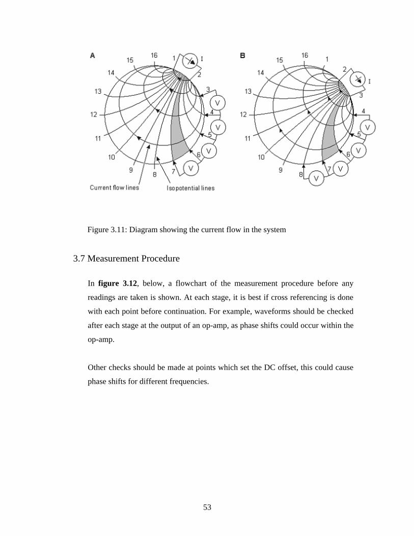
53
Figure 3.11: Diagram showing the current flow in the system
3.7 Measurement Procedure
In figure 3.12, below, a flowchart of the measurement procedure before any
readings are taken is shown. At each stage, it is best if cross referencing is done
with each point before continuation. For example, waveforms should be checked
after each stage at the output of an op-amp, as phase shifts could occur within the
op-amp.
Other checks should be made at points which set the DC offset, this could cause
phase shifts for different frequencies.
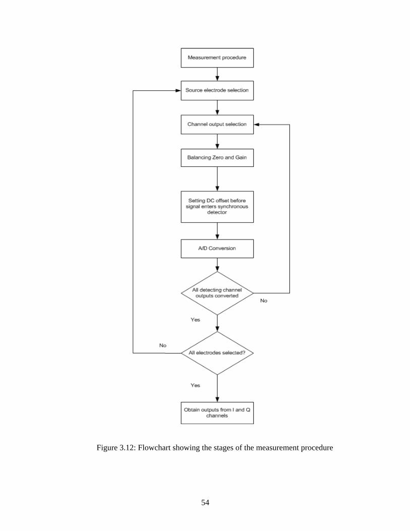
54
Figure 3.12: Flowchart showing the stages of the measurement procedure
55
3.8 Circuitry
3.8.1 AC Function Generator
The AC function generator used to drive the AC input signal is the Escort
EFG-3210 as explained in chapter 3.1. The signal driven by the function
generator into the system is kept at constant amplitude. This signal is then
adjusted for amplitude gains via a variable gain amplifier.
3.8.2 Voltage-to-Current Conversion
The voltage-to-current conversion consisted of two types, the square-wave
and the sine-wave voltage-to-current converters. By implementing
different types of current sources, different reactions would result on the
sensing side. The received AC signal is fed into the V-I converters which
in turn, converts the signal into a current source, which is then injected
into the device under test. Circuitry for the conversions and more details
of this were discussed in chapter 3.4 and 3.5.
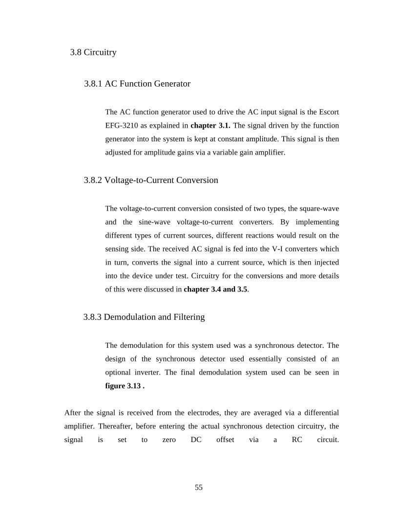
3.8.3 Demodulation and Filtering
The demodulation for this system used was a synchronous detector. The
design of the synchronous detector used essentially consisted of an
optional inverter. The final demodulation system used can be seen in
figure 3.13 .
After the signal is received from the electrodes, they are averaged via a differential
amplifier. Thereafter, before entering the actual synchronous detection circuitry, the
signal is set to zero DC offset via a RC circuit.
56
Figure 3.13: Diagram showing the final demodulation system implemented
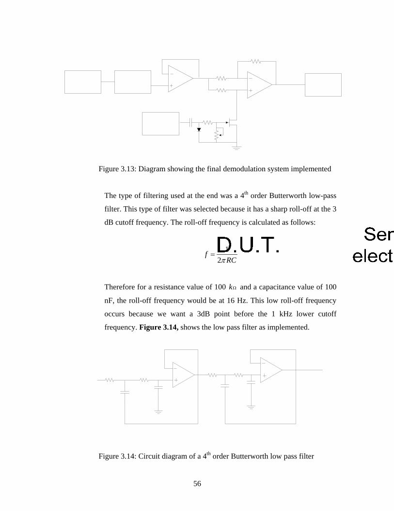
The type of filtering used at the end was a 4th order Butterworth low-pass
filter. This type of filter was selected because it has a sharp roll-off at the 3
dB cutoff frequency. The roll-off frequency is calculated as follows:
12
fRCπ
=
Therefore for a resistance value of 100 kΩ and a capacitance value of 100
nF, the roll-off frequency would be at 16 Hz. This low roll-off frequency
occurs because we want a 3dB point before the 1 kHz lower cutoff
frequency. Figure 3.14, shows the low pass filter as implemented.
Figure 3.14: Circuit diagram of a 4th order Butterworth low pass filter
57
CHAPTER 4: EXPERIMENTAL PROTOCOL AND CIRCUITRY
BUILDING
To build the whole system is not an extremely difficult task, but to create a working
system requires some circuitry analysis and skill. The designs to build included the
synchronous detector and the voltage-to-current converters.
4.1 Synchronous Detection Circuitry
The first circuitry built was the synchronous detection system. This system
constitutes of two channels, mainly, the in-phase channel, and the quadrature
channel. The in-phase channel was built first to test the circuit for its component
limitations. The type of synchronous detection circuitry used is essentially an
optional inverter. The J-FET is switched on and off at specific cycles via the
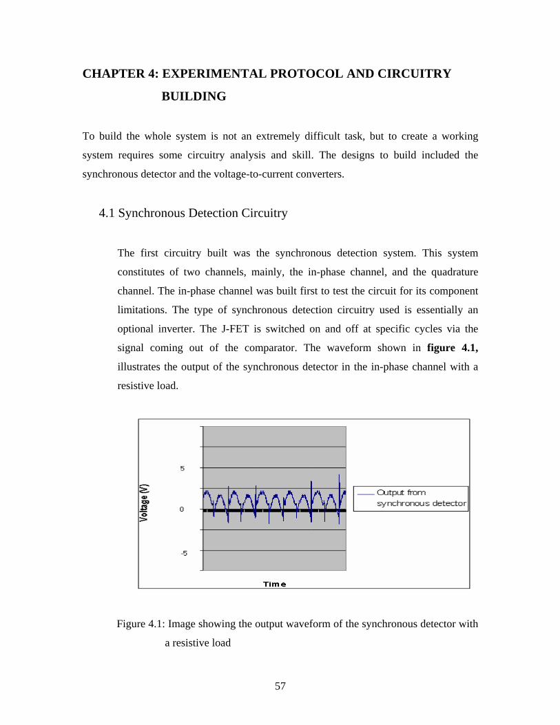
signal coming out of the comparator. The waveform shown in figure 4.1,
illustrates the output of the synchronous detector in the in-phase channel with a
resistive load.
Figure 4.1: Image showing the output waveform of the synchronous detector with
a resistive load
58
Each channel within this system needs to be tested, and the way around this is
that an actual known device is placed under test. For instance, a resistor under test
would give an output signal on the in-phase part, while a capacitive load would
give a response in the quadrature channel instead of the in-phase channel,
theoretically.
It was seen under testing that in actual fact, although by just using a resistive load
it does not in just simply give an output in the in-phase channel. While a
capacitive load would not just give an output in the quadrature channel. This is
due to the capacitance and resistance of the system or stray capacitance which
arises from the cables used for measurement. Although by implementing only a
resistive load and an output still arises from the quadrature channel, these
measurement readings are minor, as shown in chapter 5, in the test results.
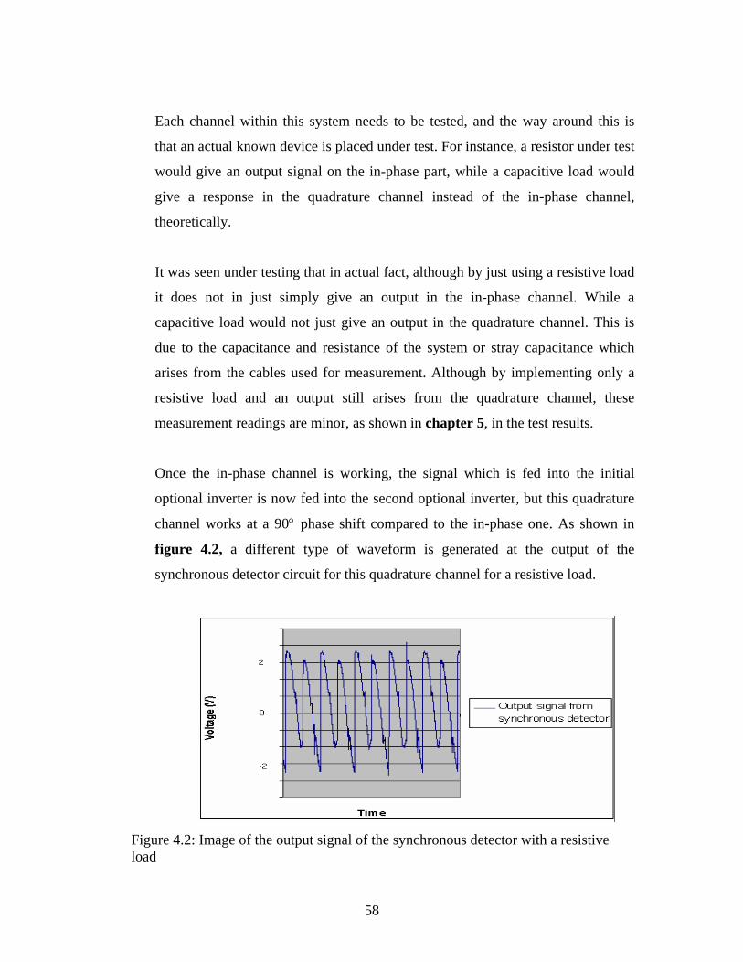
Once the in-phase channel is working, the signal which is fed into the initial
optional inverter is now fed into the second optional inverter, but this quadrature
channel works at a 90° phase shift compared to the in-phase one. As shown in
figure 4.2, a different type of waveform is generated at the output of the
synchronous detector circuit for this quadrature channel for a resistive load.
Figure 4.2: Image of the output signal of the synchronous detector with a resistive load
59
By making measurements on both in-phase and quadrature channels, the
resistance and capacitance of the load can be calculated for the device under test.
The filtering after the demodulation included a 4th order low-pass filter. This was
able to filter out the lower harmonics and other noisy signals buried within the
system, and to provide a sharp roll-off at the cutoff frequency. All the op-amps
used within this design are fast op-amps, such as the LM 351 F / TL 081 (refer to
Appendix B for data sheet), and LM 6361 (refer to Appendix B for data sheet).
4.2 Voltage to Current Converters
This section of design was slightly more complicated than the circuitry for
synchronous detection. A system such as the one used presently requires a bi-
directional current source which runs off positive and negative supply rails.
For the square-wave voltage-to-current converter, the current supplied by the
circuit is limited by the potentiometers controlling the amount of voltage input to
the circuit, as shown in figure 3.10. By including zener diodes where the signal is
injected, even smaller AC signals are allowed to enter. The zener diodes then
boost the signals creating a big-enough signal to be fed into the V-I converter.
For the sine-wave voltage-to-current converter, new modifications had to be made
to the circuit. So, in addition, circuitry was added to control the amount of
amplitude adjustment for the input signal.
Various diodes were placed in the system, as shown in figure 3.7, to prevent the
transistor from dropping in voltage, in actual fact, it limits the amount of negative
voltage drop by the transistor. In addition, figure 4.3, shows a design which was
used to create a ± 8 V supply from a ± 12 V supply. This is to prevent the op-
amps from “hitting” the rails when the transistor switches on and off. By doing so,
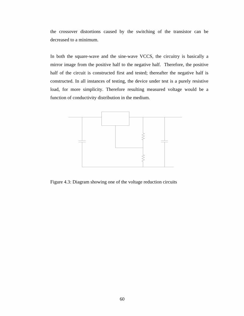
60
the crossover distortions caused by the switching of the transistor can be
decreased to a minimum.
In both the square-wave and the sine-wave VCCS, the circuitry is basically a
mirror image from the positive half to the negative half. Therefore, the positive
half of the circuit is constructed first and tested; thereafter the negative half is
constructed. In all instances of testing, the device under test is a purely resistive
load, for more simplicity. Therefore resulting measured voltage would be a
function of conductivity distribution in the medium.
Figure 4.3: Diagram showing one of the voltage reduction circuits
61
CHAPTER 5: ACTUAL TEST and RESULTS
All the following test results were implemented with the “4-electrode method” with the
electrode plates, and by using a sine-wave voltage-to-current converter. These results are
obtained by driving a constant current through the device under test and thereafter
measuring the output voltage. Discussions and analysis of results continue in chapter 6.
5.1 Test Results of a Purely Resistive Load Under Test
In order to ensure that the in-phase channel of the synchronous detection system
was working, tests had to be conducted to prove this. The test results for the
various resistive loads at different frequencies are presented below in table 1.
R 10kHz 100kHz I Channel Q Channel I Channel Q Channel
15 Ω 2mV 0 1mV (-)3mV 39 Ω 6mV 0 4mV (-)3mV 68 Ω 10mV 2mV 9mV (-)4mV 100 Ω 15mV 3mV 13mV (-)5mV 470 Ω 60mV 10mV 60mV (-)10mV 820 Ω 95mV 20mV 90mV (-)13mV
1k 110mV 26mV 105mV (-)13mV 1.8k 155mV 36mV 145mV (-)15mV 4.7k 0.225V 55mV 0.22V (-)17mV 10k 0.265V 65mV 0.26V (-)17mV
Table 1: Table of results for a resistive load under testing
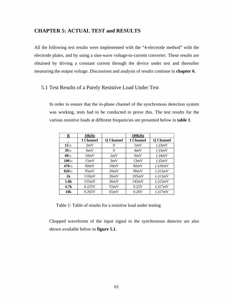
Chopped waveforms of the input signal to the synchronous detector are also
shown available below in figure 5.1.
62
(a)
(b)
Figure 5.1: Graphs showing the chopped input signals to the synchronous
detector in the in-phase channel (a) and the quadrature channel (b)
5.2 Test Results of a Purely Capacitive Load under Test
Measurements and readings taken from the quadrature channel arise from the
phase shift which occurs from the device under test. By applying a purely
capacitive load, phase shifts occur from the received output signal. This
measurement is received via the quadrature channel, which is in synchronization
with the phase shifted signal. These measurements are shown in table 2 below.
63
C 10kHz 100kHz
I Channel Q Channel I Channel Q Channel 2.2uF 0 2mV 0 0 820nF 0 4mV 0 0 680nF 0 4mv (-)2mV (-)2mV 470nF 0 6mV (-)2mV 0 220nF 0 11mV 0 0 100nF 10mV 40mV 0 2mV 47nF 12mV 60mV 0 4mV 22nF 45mV 105mV 0 11mV 15nF 90mV 130mV 0 18mV 10nF 140mV 160mV 0 22mV
Table 2: Table showing the measurement results of the quadrature channel
Various measurements and readings were also taken for known RC networks
at different frequencies. These results can be seen in Appendix C.
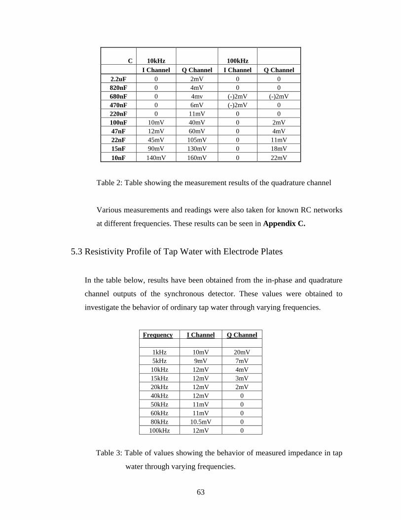
5.3 Resistivity Profile of Tap Water with Electrode Plates
In the table below, results have been obtained from the in-phase and quadrature
channel outputs of the synchronous detector. These values were obtained to
investigate the behavior of ordinary tap water through varying frequencies.
Frequency I Channel Q Channel
1kHz 10mV 20mV 5kHz 9mV 7mV 10kHz 12mV 4mV 15kHz 12mV 3mV 20kHz 12mV 2mV 40kHz 12mV 0 50kHz 11mV 0 60kHz 11mV 0 80kHz 10.5mV 0
100kHz 12mV 0
Table 3: Table of values showing the behavior of measured impedance in tap
water through varying frequencies.
64
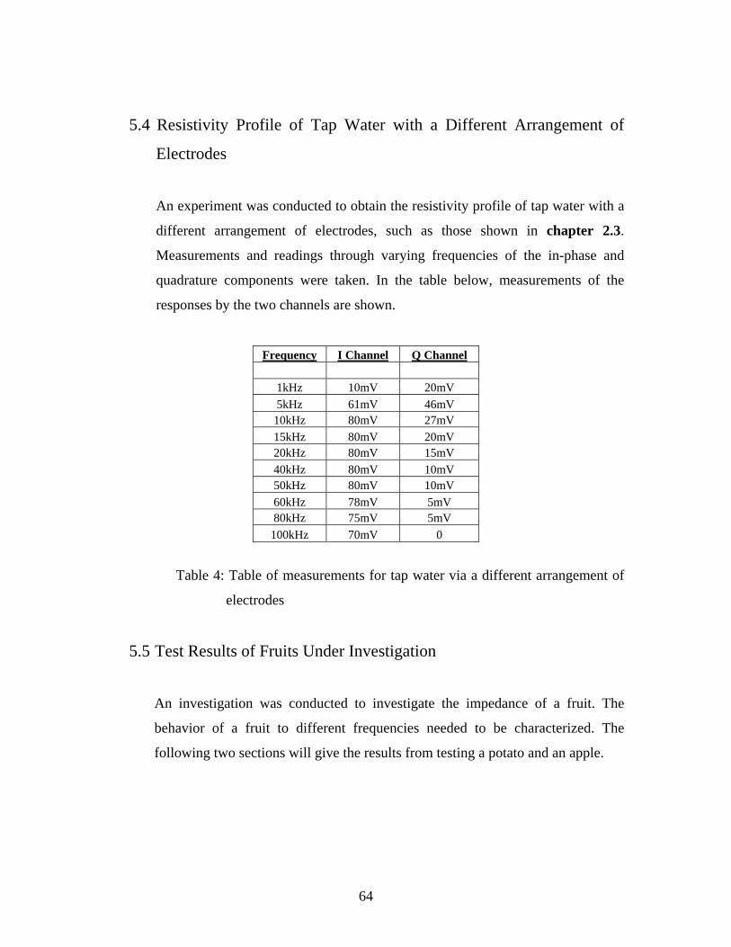
5.4 Resistivity Profile of Tap Water with a Different Arrangement of
Electrodes
An experiment was conducted to obtain the resistivity profile of tap water with a
different arrangement of electrodes, such as those shown in chapter 2.3.
Measurements and readings through varying frequencies of the in-phase and
quadrature components were taken. In the table below, measurements of the
responses by the two channels are shown.
Frequency I Channel Q Channel
1kHz 10mV 20mV 5kHz 61mV 46mV 10kHz 80mV 27mV 15kHz 80mV 20mV 20kHz 80mV 15mV 40kHz 80mV 10mV 50kHz 80mV 10mV 60kHz 78mV 5mV 80kHz 75mV 5mV
100kHz 70mV 0
Table 4: Table of measurements for tap water via a different arrangement of
electrodes
5.5 Test Results of Fruits Under Investigation
An investigation was conducted to investigate the impedance of a fruit. The
behavior of a fruit to different frequencies needed to be characterized. The
following two sections will give the results from testing a potato and an apple.
65
5.5.1 Potato
Results are obtained from the in-phase and quadrature component of the
synchronous detector. In table 5, changes in amplitude and phase are shown
through varying frequencies for the potato under testing.
Frequency I Q
1kHz 2mV 5mV 5kHz 8mV 13mV 10kHz 8mV 10mV 15kHz 5mV 8mV 20kHz 4mV 7mV 40kHz 1mV 4mV 50kHz 0 4mV 60kHz 0 3mV 80kHz 0 2mV
100kHz 0 2mV
Table 5: Table indicating the behavior of a potato through varying frequencies
5.5.2 Apple
The following table shows the response for the two channels, of an apple
affected by varying frequencies.
Frequency I Channel Q Channel
1kHz 8mV 13mV 5kHz 22mV 38mV 10kHz 26mV 25mV 15kHz 20mV 20mV 20kHz 17mV 17mV 40kHz 11mV 10mV 50kHz 10mV 9mV 60kHz 8mV 7mV 80kHz 7mV 5mV
100kHz 6mV 4mV Table 6: Table indicating the behavior of an apple through varying
frequencies
66
CHAPTER 6: INTERPRETATIONS AND DISCUSSIONS OF
RESULTS
Interpretations and analysis of the data which was acquired in measurement is discussed
in this chapter. Graphs and responses are also formed from the results of the previous
chapter for analysis.
6.1 An example of the measurement system
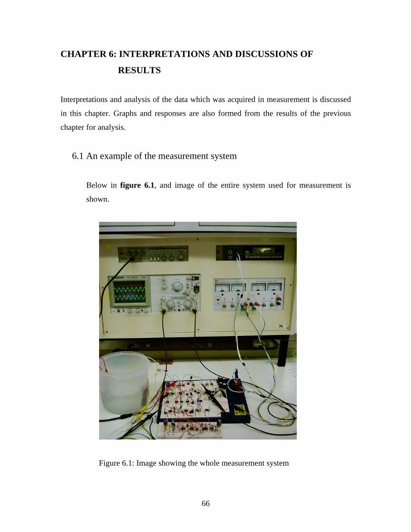
Below in figure 6.1, and image of the entire system used for measurement is
shown.
Figure 6.1: Image showing the whole measurement system
67
6.2 Measurement Techniques and Equipment Limitations
Measurement and readings were taken by obtaining values straight from the
oscilloscope. Therefore, there is a possibility that errors would occur. A ± 10%
error chance should be allowed for measurements that are taken. As shown in
chapter 5, for resistors, values up to 100 kΩ was measured, but in the graphs
showing the results below, for simplicity sake, the first ten measurement values
are shown. The same is applied for the capacitive measurements.
In addition, for the filtering stages, towards the end, a 4th order low pass
Butterworth filter was implemented. This filter did not have any gain on it, but as
we see from the results shown in chapter 5, the system was quite sensitive to the
changes in the load impedance. In order to achieve more accurate readings, a gain
should be included for a clearer indication of the readings.
6.2.1 Probe-to-probe and Measurement Errors
All the measurements were taken via the oscilloscope probes. The
disadvantage of this is that the wiring cable of these probes is almost 1m
long, therefore, minor errors could be caused by it. Other disadvantages are
that the cables of the oscilloscopes are not perfectly shielded, in which case,
stray capacitance measurements could arise under testing.
Although when using the probes for measurement, probe measurement
values are already placed on a X10 probe therefore decreasing the
possibility for error created by the probe itself, but errors are inevitable.
68
6.2.2 Circuit Board
The circuit board used for the designs of the circuitry used was provided.
Nothing in industry is made perfectly, therefore minor stray capacitance
values may arise in between the tracks of the circuit board which were used.
Another disadvantage of using the circuit board is that components are
plugged into the circuit and pieces of wires are used to connect different
parts of the circuit together. These wires may touch each other occasionally,
therefore causing minor capacitive, and error values in the final output.
6.2.3 Components
The components used for this research was the components which were
available. No additional components were bought. Various op-amps were
used for this experiment, the LM 6361, LM 6461, and the LM 351 F / TCL
081, all the specifics of these chips are shown in the data sheet available in
the Appendix B.
Components, such as resistors and capacitors which were used also have
tolerance within them. For resistors used, tolerance of error is roughly 5%
from the original value.
Various other components may have tolerance within them, therefore all of
these needs to be considered when measuring a certain part of a signal from
the system.
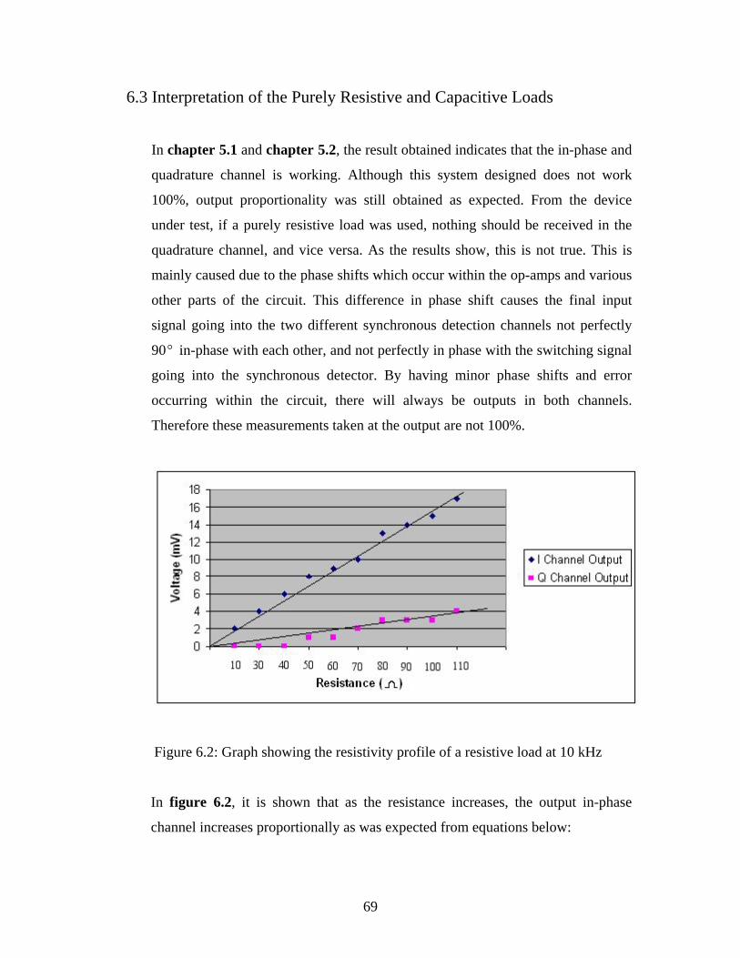
69
6.3 Interpretation of the Purely Resistive and Capacitive Loads
In chapter 5.1 and chapter 5.2, the result obtained indicates that the in-phase and
quadrature channel is working. Although this system designed does not work
100%, output proportionality was still obtained as expected. From the device
under test, if a purely resistive load was used, nothing should be received in the
quadrature channel, and vice versa. As the results show, this is not true. This is
mainly caused due to the phase shifts which occur within the op-amps and various
other parts of the circuit. This difference in phase shift causes the final input
signal going into the two different synchronous detection channels not perfectly
90 ° in-phase with each other, and not perfectly in phase with the switching signal
going into the synchronous detector. By having minor phase shifts and error
occurring within the circuit, there will always be outputs in both channels.
Therefore these measurements taken at the output are not 100%.
Figure 6.2: Graph showing the resistivity profile of a resistive load at 10 kHz
In figure 6.2, it is shown that as the resistance increases, the output in-phase
channel increases proportionally as was expected from equations below:
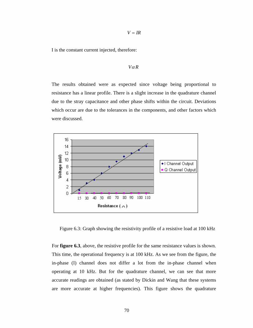
70
V IR=
I is the constant current injected, therefore:
V Rα
The results obtained were as expected since voltage being proportional to
resistance has a linear profile. There is a slight increase in the quadrature channel
due to the stray capacitance and other phase shifts within the circuit. Deviations
which occur are due to the tolerances in the components, and other factors which
were discussed.
Figure 6.3: Graph showing the resistivity profile of a resistive load at 100 kHz
For figure 6.3, above, the resistive profile for the same resistance values is shown.
This time, the operational frequency is at 100 kHz. As we see from the figure, the
in-phase (I) channel does not differ a lot from the in-phase channel when
operating at 10 kHz. But for the quadrature channel, we can see that more
accurate readings are obtained (as stated by Dickin and Wang that these systems
are more accurate at higher frequencies). This figure shows the quadrature
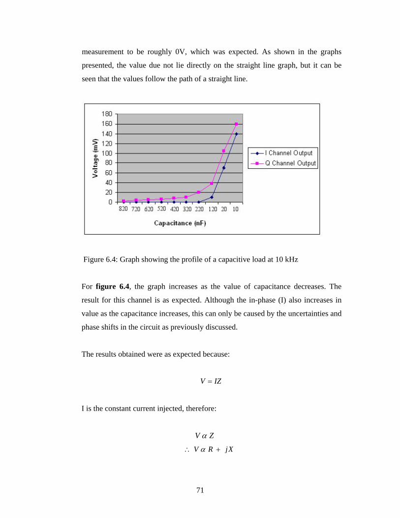
71
measurement to be roughly 0V, which was expected. As shown in the graphs
presented, the value due not lie directly on the straight line graph, but it can be
seen that the values follow the path of a straight line.
Figure 6.4: Graph showing the profile of a capacitive load at 10 kHz
For figure 6.4, the graph increases as the value of capacitance decreases. The
result for this channel is as expected. Although the in-phase (I) also increases in
value as the capacitance increases, this can only be caused by the uncertainties and
phase shifts in the circuit as previously discussed.
The results obtained were as expected because:
V IZ=
I is the constant current injected, therefore:
V Zα
V R jXα∴ +
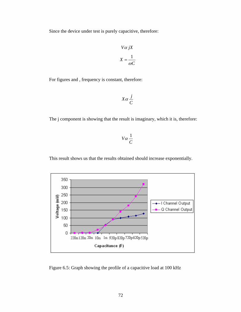
72
Since the device under test is purely capacitive, therefore:
V jXα
1XCω
=
For figures and , frequency is constant, therefore:
jXC
α
The j component is showing that the result is imaginary, which it is, therefore:
1VC
α
This result shows us that the results obtained should increase exponentially.
Figure 6.5: Graph showing the profile of a capacitive load at 100 kHz
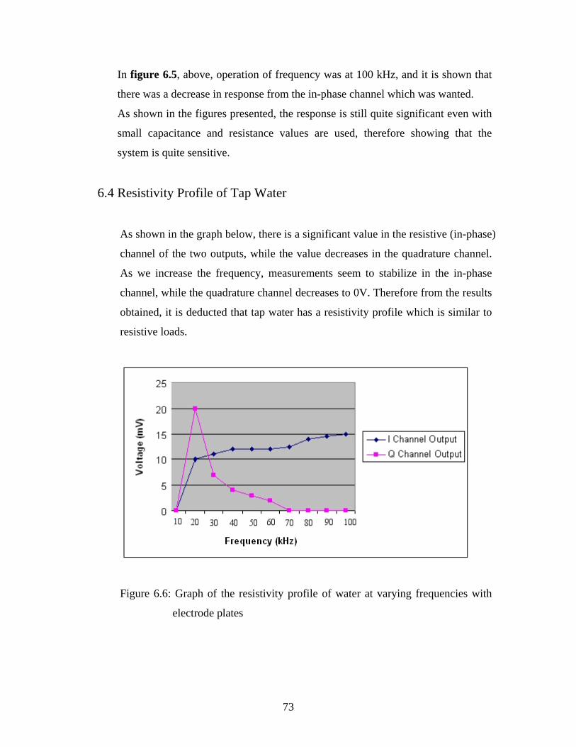
73
In figure 6.5, above, operation of frequency was at 100 kHz, and it is shown that
there was a decrease in response from the in-phase channel which was wanted.
As shown in the figures presented, the response is still quite significant even with
small capacitance and resistance values are used, therefore showing that the
system is quite sensitive.
6.4 Resistivity Profile of Tap Water
As shown in the graph below, there is a significant value in the resistive (in-phase)
channel of the two outputs, while the value decreases in the quadrature channel.
As we increase the frequency, measurements seem to stabilize in the in-phase
channel, while the quadrature channel decreases to 0V. Therefore from the results
obtained, it is deducted that tap water has a resistivity profile which is similar to
resistive loads.
Figure 6.6: Graph of the resistivity profile of water at varying frequencies with
electrode plates
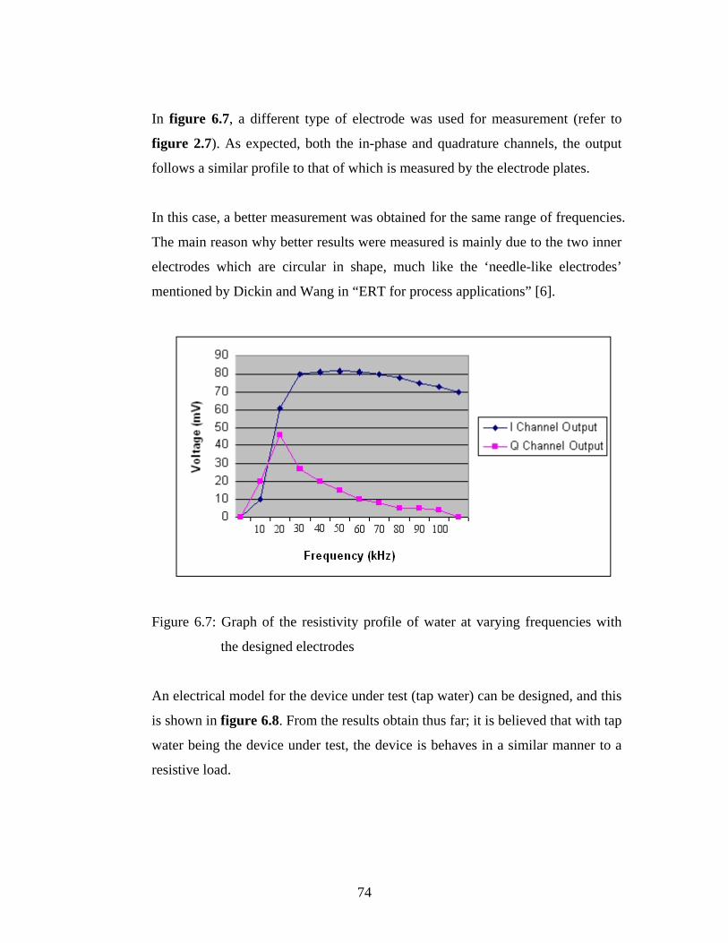
74
In figure 6.7, a different type of electrode was used for measurement (refer to
figure 2.7). As expected, both the in-phase and quadrature channels, the output
follows a similar profile to that of which is measured by the electrode plates.
In this case, a better measurement was obtained for the same range of frequencies.
The main reason why better results were measured is mainly due to the two inner
electrodes which are circular in shape, much like the ‘needle-like electrodes’
mentioned by Dickin and Wang in “ERT for process applications” [6].
Figure 6.7: Graph of the resistivity profile of water at varying frequencies with
the designed electrodes
An electrical model for the device under test (tap water) can be designed, and this
is shown in figure 6.8. From the results obtain thus far; it is believed that with tap
water being the device under test, the device is behaves in a similar manner to a
resistive load.
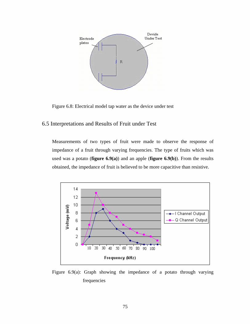
75
Figure 6.8: Electrical model tap water as the device under test
6.5 Interpretations and Results of Fruit under Test
Measurements of two types of fruit were made to observe the response of
impedance of a fruit through varying frequencies. The type of fruits which was
used was a potato (figure 6.9(a)) and an apple (figure 6.9(b)). From the results
obtained, the impedance of fruit is believed to be more capacitive than resistive.
Figure 6.9(a): Graph showing the impedance of a potato through varying
frequencies
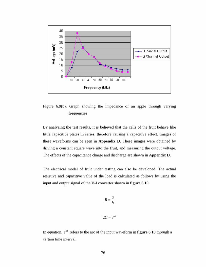
76
Figure 6.9(b): Graph showing the impedance of an apple through varying
frequencies
By analyzing the test results, it is believed that the cells of the fruit behave like
little capacitive plates in series, therefore causing a capacitive effect. Images of
these waveforms can be seen in Appendix D. These images were obtained by
driving a constant square wave into the fruit, and measuring the output voltage.
The effects of the capacitance charge and discharge are shown in Appendix D.
The electrical model of fruit under testing can also be developed. The actual
resistive and capacitive value of the load is calculated as follows by using the
input and output signal of the V-I converter shown in figure 6.10.
aRb
=
2 tC eα=
In equation, teα refers to the arc of the input waveform in figure 6.10 through a
certain time interval.
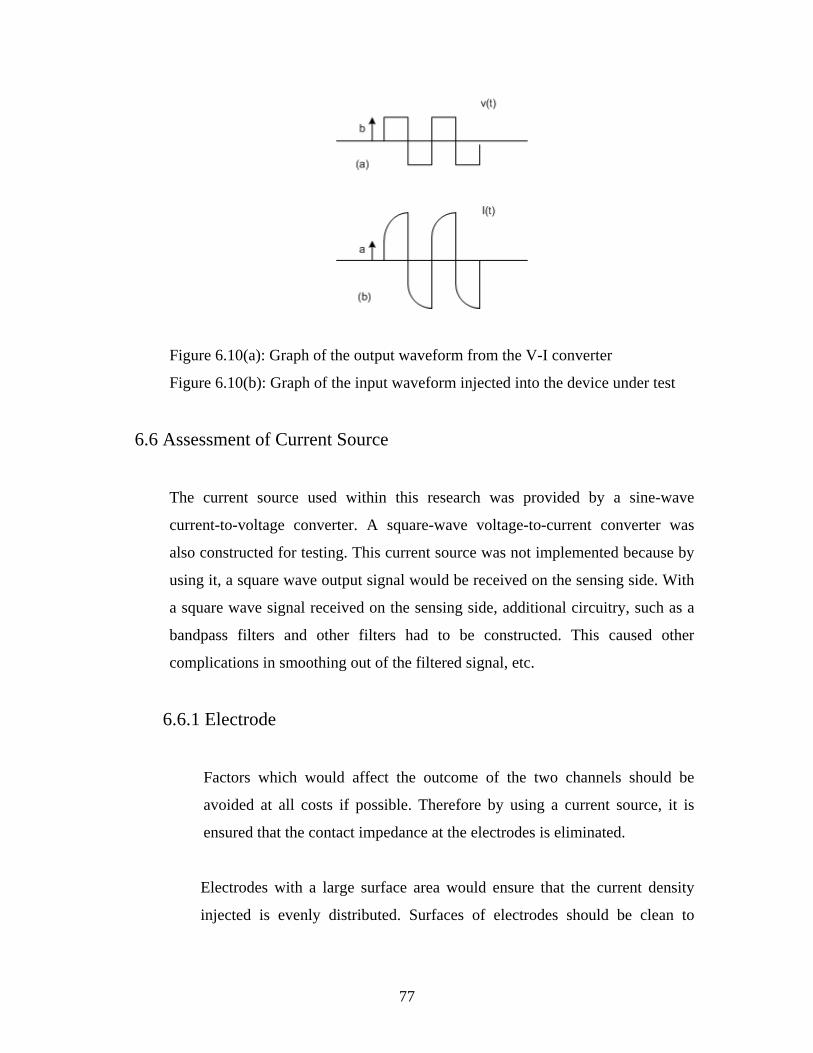
77
Figure 6.10(a): Graph of the output waveform from the V-I converter
Figure 6.10(b): Graph of the input waveform injected into the device under test
6.6 Assessment of Current Source
The current source used within this research was provided by a sine-wave
current-to-voltage converter. A square-wave voltage-to-current converter was
also constructed for testing. This current source was not implemented because by
using it, a square wave output signal would be received on the sensing side. With
a square wave signal received on the sensing side, additional circuitry, such as a
bandpass filters and other filters had to be constructed. This caused other
complications in smoothing out of the filtered signal, etc.
6.6.1 Electrode
Factors which would affect the outcome of the two channels should be
avoided at all costs if possible. Therefore by using a current source, it is
ensured that the contact impedance at the electrodes is eliminated.
Electrodes with a large surface area would ensure that the current density
injected is evenly distributed. Surfaces of electrodes should be clean to
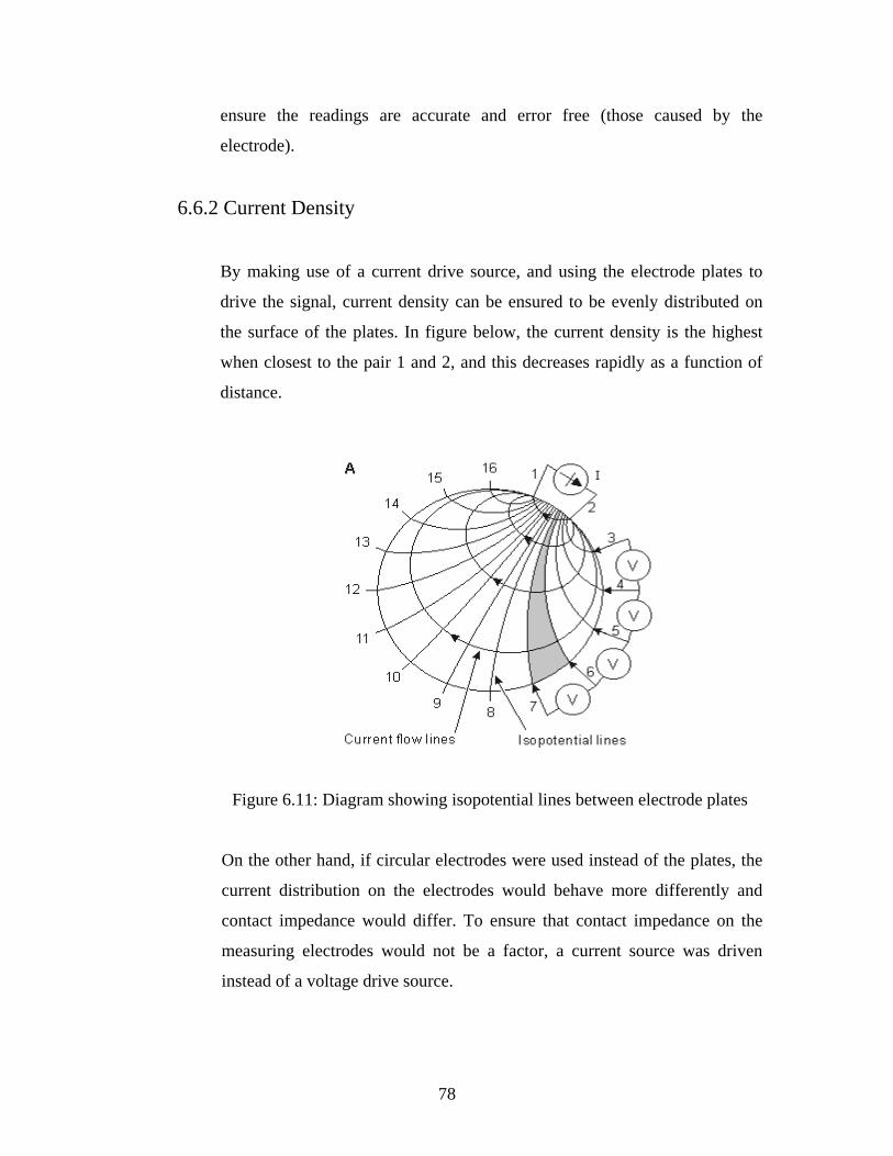
78
ensure the readings are accurate and error free (those caused by the
electrode).
6.6.2 Current Density
By making use of a current drive source, and using the electrode plates to
drive the signal, current density can be ensured to be evenly distributed on
the surface of the plates. In figure below, the current density is the highest
when closest to the pair 1 and 2, and this decreases rapidly as a function of
distance.
Figure 6.11: Diagram showing isopotential lines between electrode plates
On the other hand, if circular electrodes were used instead of the plates, the
current distribution on the electrodes would behave more differently and
contact impedance would differ. To ensure that contact impedance on the
measuring electrodes would not be a factor, a current source was driven
instead of a voltage drive source.
79
A voltage measurement with high input impedance op-amps eliminated the
effects of contact impedance on the sensor side.
6.7 Limitations of Current Sensor
Limitations of the current sensor implemented were due to the op-amps used, their
speeds and their gain bandwidths. Another limitation is also the vessel used for a
liquid device under test. By using a significantly different shape or sized vessel for
testing would probably have different effects on the injected and received
waveform? This factors needs to be investigated further. Other form of shapes and
sizes of electrodes could also be used to have a different impact.
6.7.1 Sensitivity
As shown in the test results in chapter 5, this system is actually quite
sensitive to changes in the load. As was shown in chapter 6 above, the
response of the in-phase and quadrature channel increased or decreased
proportionally with the changes in resistive and capacitive loads.
Input signals fed into the V-I converter were also quite small, therefore with
a relatively small signal, we were able to drive the whole system.
By implementing a gain of ± 10 on the low-pass filter increases the output
signal, therefore showing significant changes in sensitivity on the received
signal. In addition, it is vital to ensure that the electrodes are stationary
during measurements made through different frequencies. Changing the
positioning of the electrodes will either increase or decrease the amplitude of
the signal received, therefore affecting the final output in the two channels.
NOTE: Images of actual measurement of various objects under test are shown in
Appendix D
80
CHAPTER 7: CONCLUSIONS
The following conclusions were reached:
1. A low cost, easy to use measurement technique for electrical impedance tomography
via synchronous detection has been implemented. Two types of voltage-to-current
converters have been used to characterize its response with the EIT measurement
results. It was decided after testing that the sine-wave voltage-to-current converter was
simpler in this instance and therefore should be used.
2. Relevant information has been obtained from the synchronous detection measurement
system for electrical impedance tomography. Although the readings taken for
measurement of various devices may not have been accurate, these results are,
however, repeatable and therefore we are able to characterize the sensitivity of the
system and its performance.
3. It is proven that by using a voltage controlled current source to drive the input signal
into the synchronous detection system, and measuring the differential voltage output
has many advantages as explained in chapter 3 and chapter 5. The disadvantage
established when implementing the voltage controlled current source is that a bi-
directional voltage-to-current converter without distortion is difficult to create for high
frequencies. By disregarding this factor and employing a voltage drive source would be
unfeasible and could cause many unwanted effects at the sensing stages of the design
which will affect the final output.
4. Data collection using the current system designed has been successfully tested at a
frequency of 100 kHz. Reasonable outputs have been obtained from the system at
frequencies of up to 300 kHz, with distortion occurring beyond that.
5. Two different types of electrodes have been implemented in this research, and the
responses from them have been recorded. Although the two types of electrodes were

81
used for measurements of tap water, nevertheless, the readings show that the
impedance behavior follows a similar profile for both types of electrodes.
6. The system in general was quite sensitive to changes in the resistive and capacitive
loads of the system. It was shown in the results that by changes the resistive and
capacitive values, the output stages would increase and decrease proportionally. By
using a gain on the filtering stages after the demodulator, sensitivity of the system can
be shown even more clearly and can be characterized easily.
82
CHAPTER 8: RECOMMENDATIONS FOR FUTURE WORK AND
DEVELOPMENT
The work completed for this thesis implemented a working electrical impedance
tomography measurement system. From the investigations and results, much
understanding was gained on several issues in this measurement system, which leads to
suggestions for improvement and implementations of other concepts. Suggestions and
guidelines are provided in this chapter.
8.1 The Role of Current Source
Current source played a vital role in the input signal which was injected. It is
recommended that a current drive system should be implemented to eliminate
effects of contact impedance on the surfaces of the measuring electrodes. By
applying a current driven system, the algorithm reconstruction which could be
done for the output is much simpler as opposed to a voltage driven system.
8.2 Different Types of Sensor Design
Essentially, two different types of electrodes were used in measurement. Other type
of electrode’s shapes and sizes should be investigated to compare their
performance and reliability. By using a current driven system, the behavior of
current density on the electrodes should be kept in mind; therefore the driving pair
of electrodes should not be too small. Different arrangements of electrodes within
the vessel can also be investigated.
Different measurement techniques could also be implemented, such as the cross
and opposite method suggested by Hua, Webster, and Tompkins (1987). The
methods proposed could be implemented and compared to that of the present
system design.
83
8.3 Recommendations
The specific recommendations for future work are:
1. Further testing of results is required for a more accurate profile of the behavior
of the various devices under test. Better and more accurate measurement op-
amps could be acquired to fit within the system created for more accurate
readings. Op-amps created are never perfect; therefore, it is vital to ensure that
phase shifts of the signal after going through an op-amp should not be phase
shifted. At the filtering stages, a gain should be included to observe a better
sensitivity profile.
2. A rig / vessel whereby the electrode plates are to be mounted onto the surface
of the vessel is to be built in order for the readings taken at the output be
unaffected by the movement in the electrodes.
3. The measurement system built can be incorporated within the existing
measurement system. The system constructed can be incorporated into the 4-
layered sensor multiplexing system available, and adjusted for measurement.
Measurements and readings can be done for all four layers of sensors and a
switching system can be constructed for measurements taken between the four
layers.

84
LIST OF REFERENCES
[1] M.S. Beck, R.A. Williams
‘Process tomography: a European innovation and its applications’
15 January 1996
[2] J.O. Bockris, S.U.M Khan
‘Surface Electrochemistry, A Molecular Level Approach (New York: Plenum’
1993
[3] B.H. Brown and A.D. Segar
‘The Sheffield data collection system’
1985
[4] J.J. Cilliers, W. Xie, S.J. Neethling, E.W. Randall, A.J. Wilkinson
‘Electrical resistance tomography using a bi-directional current pulse technique’
31 May 2001
[5] D.A.L. Collie , J.J.A van Weereld, and M.A. Player
‘A fast resistance measurement system for impedance tomography using a bipolar
DC pulse method’
14 June 2001
[6] F. Dickin, M. Wang
‘Electrical resistance tomography for process applications’
8 January 1996

85
[7] Prof. J. Greene
‘EEE485F Systematic Electronic Design course notes’
Department of Electrical Engineering
University of Cape Town
[8] L.M. Heikkinen, M. Vauhkonen, T. Savolainen and J.P. Kaipio
‘Modeling of internal structures and electrodes in electrical process tomography ’
20 March 2001
[9] P. Hua, J.G. Webster, and W.J. Tompkins
‘Effect of the measurement method on noise handling and image quality of EIT
imaging’
IEEE 9th Annual Conf. on Engineering in Medicine and Biological Science
Pg. 1429-1430
[10] F.J. Lidgey and Q.C. Zhu
‘Electrode current determination from programmable voltage source’
September 1991
[11] National Research Council, National Academy Press, Washington D.C.
‘Mathematics and Physics of Emerging Biomedical Imaging’
1996
[12] J.G. Webster
‘Electrical Impedance Tomography’
1990

86
[13] Dr. A.J. Wilkinson
‘EEE358S Telecommunications course notes’
Department of Electrical Engineering
University of Cape Town
[14] W.Q. Yang
‘Hardware design of electrical capacitance tomography’
14 September 1995
[15] W.Q. Yang
‘Further developments in an ac-based capacitance tomography system’
18 July 2001
[16] W.Q. Yang, T.A. York
‘New AC-based capacitance tomography system’
11 June 1998
[17]] Trevor York
‘Status of Electrical tomography in industrial applications’
9 March 2001
[19] http://circuits.cf.ac.uk/group/research/med/
09/2003
[20] http://26_ Impedance Tomography.htm
09/2003
[21] http://www.geocities.com/CapeCanaveral/9710/html/eit.html
10/2003
[22] http://zeta.msri.org/calendar/workshops/WksInfo/10/show_info
14/10/2003

87
BIBLIOGRAPHY
[1] D. Halliday, R. Resnick and J. Walker
‘Fundamentals of Physics Extended 5th ed. ‘New York: John Wiley & Son
1997
[2] P. Horowitz and W. Hill
‘The Art of Electronics 2nd ed. Cambridge University Press’
1997
[3] P.A.T. Pinheiro, W.W. Loh and F.J. Dickin
‘Internal sized electrodes for electrical resistance tomography’ Electronics Letters
8 January 1998
[4] P.A.T. Pinheiro, W.W. Loh, M.Wang, R. Mann and R.C. Waterfall
‘Three Dimensional electrical resistance tomography in a stirred mixing vessel’
25 June 1998
[5] R.A. Williams, M.S. Beck
‘Process Tomography, Principle, Techniques and Applications’
pg. 49-82
1998
[6] U. Tietze, Ch. Schenk
‘Advanced electronic circuits’
pg. 53-64
1978

88
APPENDIX A - DATA SHEET OF ESCORT
EFG-3210 FUNCTION GENERATOR
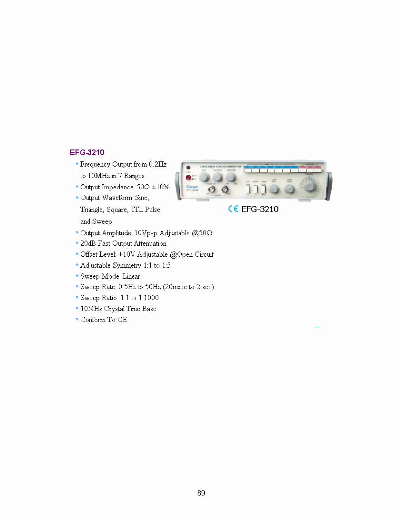
89

90
APPENDIX B – DATA SHEETS
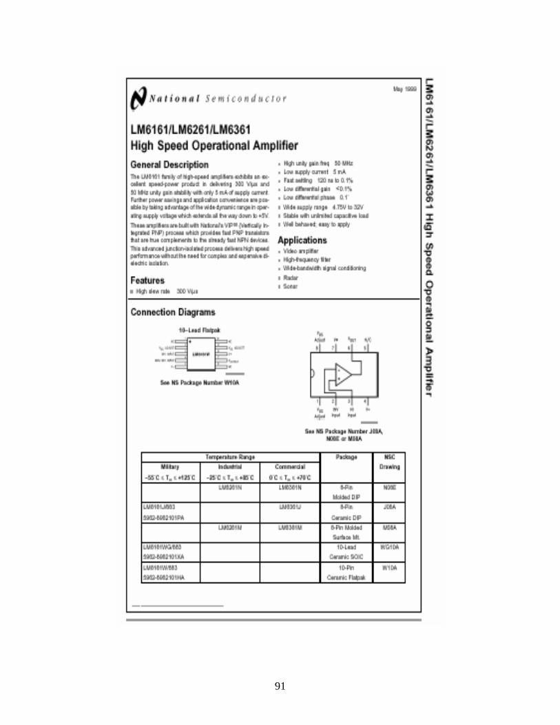
91
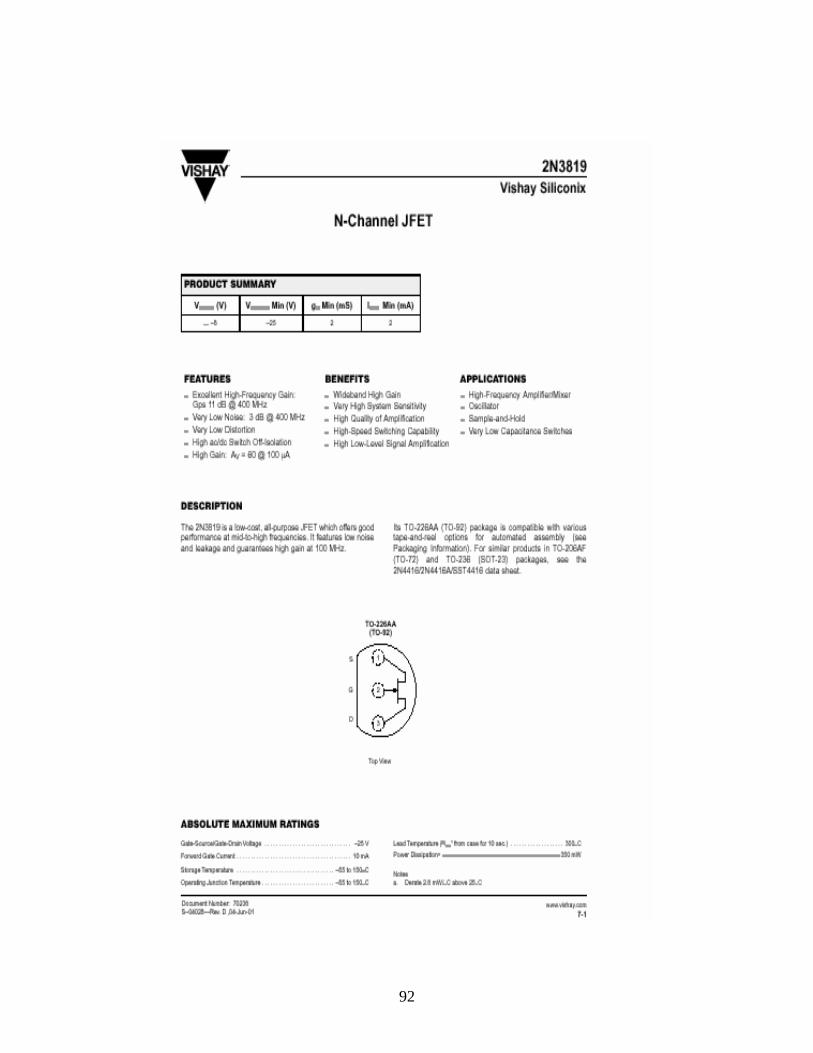
92
93
94
95

96
APPENDIX C - ADDITIONAL TEST RESULTS
OF KNOWN NETWORKS
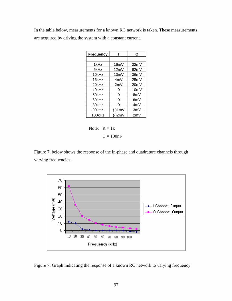
97
In the table below, measurements for a known RC network is taken. These measurements
are acquired by driving the system with a constant current.
Frequency I Q
1kHz 16mV 22mV 5kHz 12mV 62mV 10kHz 10mV 36mV 15kHz 4mV 25mV 20kHz 2mV 20mV 40kHz 0 10mV 50kHz 0 8mV 60kHz 0 6mV 80kHz 0 4mV 90kHz (-)1mV 3mV
100kHz (-)2mV 2mV
Note: R = 1k
C = 100nF
Figure 7, below shows the response of the in-phase and quadrature channels through
varying frequencies.
Figure 7: Graph indicating the response of a known RC network to varying frequency
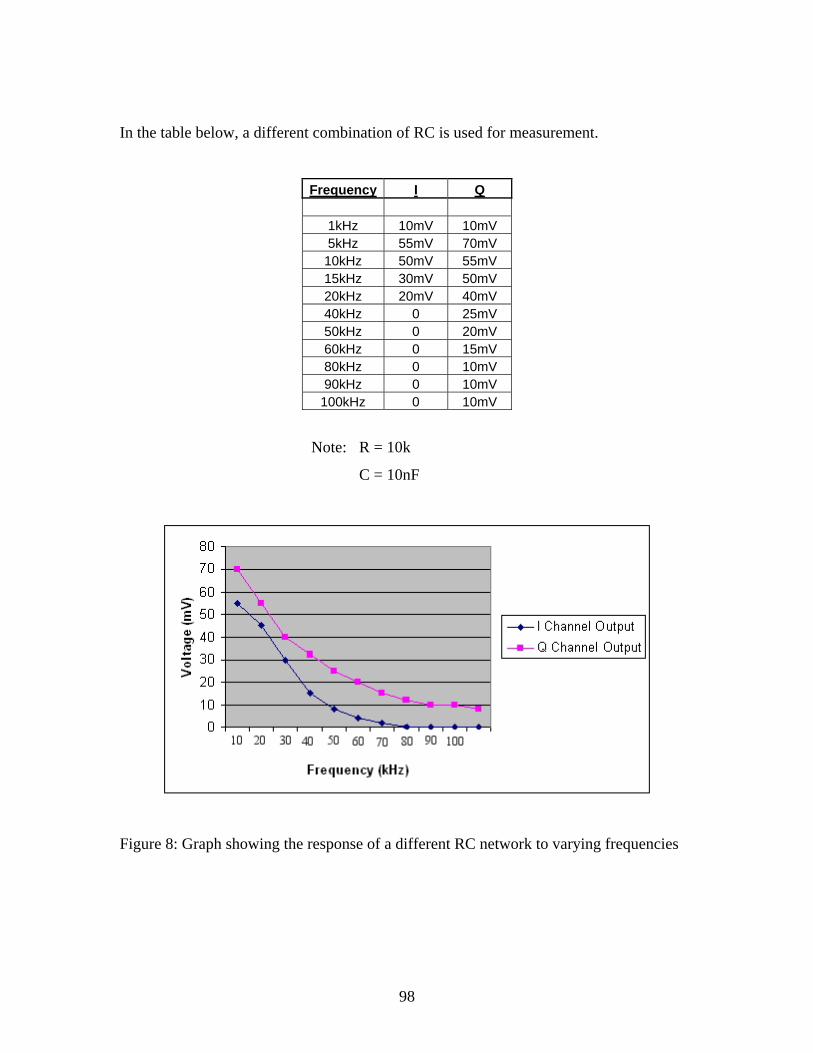
98
In the table below, a different combination of RC is used for measurement.
Frequency I Q
1kHz 10mV 10mV 5kHz 55mV 70mV 10kHz 50mV 55mV 15kHz 30mV 50mV 20kHz 20mV 40mV 40kHz 0 25mV 50kHz 0 20mV 60kHz 0 15mV 80kHz 0 10mV 90kHz 0 10mV
100kHz 0 10mV
Note: R = 10k
C = 10nF
Figure 8: Graph showing the response of a different RC network to varying frequencies
99
APPENDIX D - IMAGES OF ACTUAL
MEASUREMENTS TAKEN
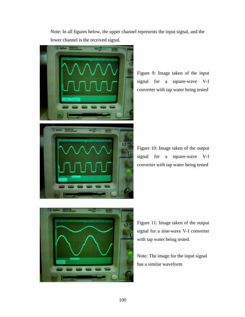
100
Note: In all figures below, the upper channel represents the input signal, and the
lower channel is the received signal.
Figure 9: Image taken of the input
signal for a square-wave V-I
converter with tap water being tested
Figure 10: Image taken of the output
signal for a square-wave V-I
converter with tap water being tested
Figure 11: Image taken of the output
signal for a sine-wave V-I converter
with tap water being tested.
Note: The image for the input signal
has a similar waveform
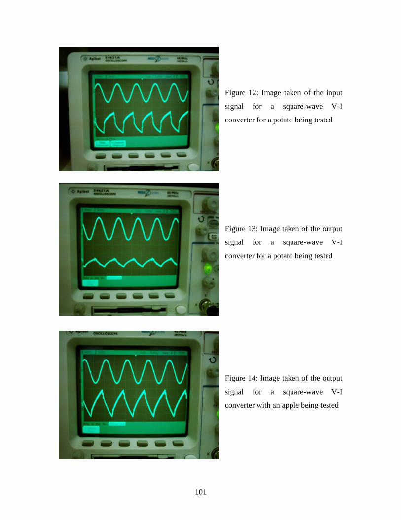
101
Figure 12: Image taken of the input
signal for a square-wave V-I
converter for a potato being tested
Figure 13: Image taken of the output
signal for a square-wave V-I
converter for a potato being tested
Figure 14: Image taken of the output
signal for a square-wave V-I
converter with an apple being tested
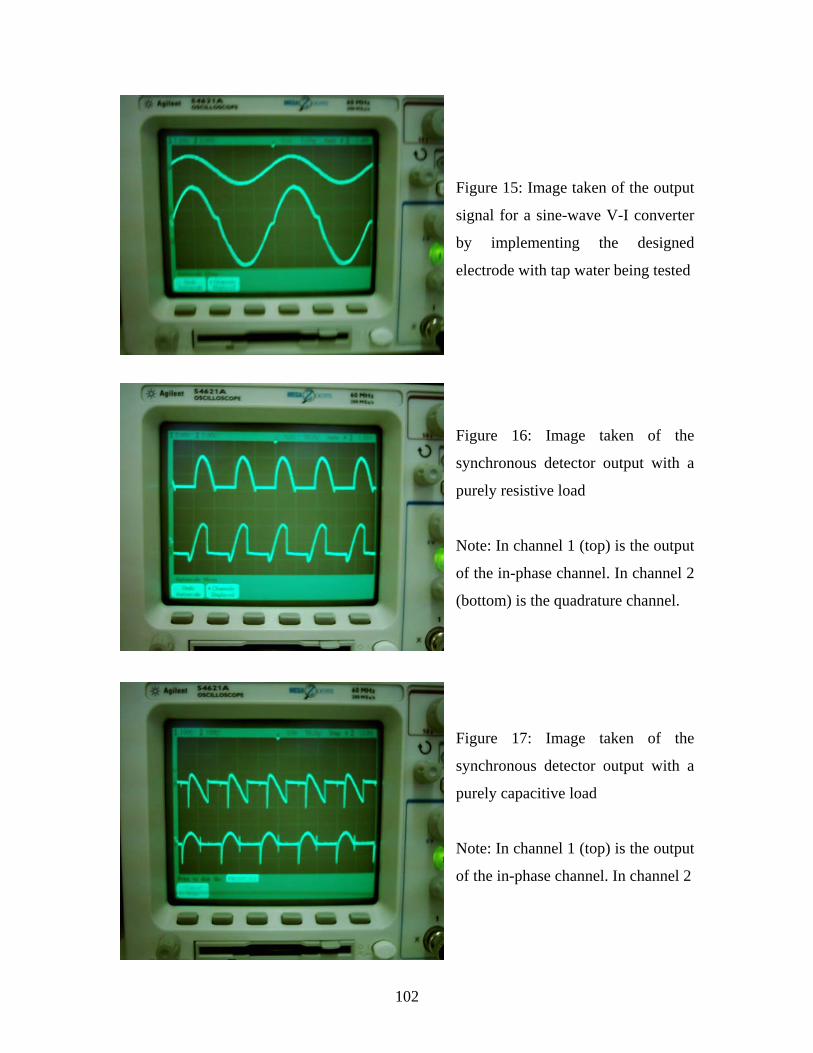
102
Figure 15: Image taken of the output
signal for a sine-wave V-I converter
by implementing the designed
electrode with tap water being tested
Figure 16: Image taken of the
synchronous detector output with a
purely resistive load
Note: In channel 1 (top) is the output
of the in-phase channel. In channel 2
(bottom) is the quadrature channel.
Figure 17: Image taken of the
synchronous detector output with a
purely capacitive load
Note: In channel 1 (top) is the output
of the in-phase channel. In channel 2


![electrical impedance tomography - Aaltolib.tkk.fi/Diss/2008/isbn9789512296804/article1.pdf · [I] Two-stage reconstruction of a circular anomaly in electrical impedance tomography](https://static.fdocuments.us/doc/165x107/5b7a88557f8b9a22238c5728/electrical-impedance-tomography-i-two-stage-reconstruction-of-a-circular.jpg)