Electric Circuits - Urząd Miasta Łodzimatel.p.lodz.pl/wee/i12zet/Electric Circuits.pdfPreface This...
172
Michał Tadeusiewicz Electric Circuits Technical University of Łódź International Faculty of Engineering Łódź 2009
-
Upload
truonghanh -
Category
Documents
-
view
214 -
download
1
Transcript of Electric Circuits - Urząd Miasta Łodzimatel.p.lodz.pl/wee/i12zet/Electric Circuits.pdfPreface This...

Michał Tadeusiewicz
Electric Circuits
Technical University of Łódź International Faculty of Engineering
Łódź 2009

Contents
Preface…………………………………………………….. 5
1. Fundamental laws of electrical circuits…………………… 7 1.1. Introduction ............................................................. 7 1.2. Kirchhoff’s Voltage Law (KVL).............................. 8 1.3. Kirchhoff’s Current Law (KCL)................….......... 10 1.4. Independence of KCL equations………………….. 12 1.5. Independence of KVL equations………………….. 13 1.6. Tellegen’s theorem………………………………... 14
2. Circuit elements.................................................................... 16 2.1. Resistors ................................................................... 16 2.2. Independent sources………………………………. 18
3. Power and energy…………………………………………. 24
4. Simple linear resistive circuits……………………………. 26
5. Resistive circuits. DC analysis……………………………. 30 5.1. Superposition theorem and its application………… 30
6. Three terminal resistive circuits…………………………... 35
7. The Thevenin-Norton theorem……………………………. 40
8. Node method……………………………………………… 47
9. Simple nonlinear circuits………………………………….. 53
10. Controlled sources………………………………………… 59
11. Capacitor……………………………...…………………... 61 11.1. Introduction.............................................................. 61 11.2. Continuity property……………………………….. 64
11.3. Energy stored in a capacitor………………………. 65 11.4. Series connection of capacitors…………………… 66 11.5. Parallel connection of capacitors………………….. 68
12. Inductor…………………………………………………… 69 12.1. Introduction.............................................................. 69 12.2. Continuity property………………………………... 72 12.3. Hysteresis………………………………………….. 73 12.4. Energy stored in an inductor……………………… 74 12.5. Series connection of inductors…………………….. 75 12.6. Parallel connection of inductors…………………... 76
13. Operational-amplifier circuits…………………………….. 78 13.1. Description of the operational amplifier................... 78 13.2. Examples………………………………………….. 82 13.3. Finite gain model of the operational amplifier......... 85
14. First order circuits driven by DC sources…………………. 88 14.1. Resistor-inductor circuits............................……...... 88 14.2. Resistor-capacitor circuits………………………… 96
15. Sinusoidal steady-state analysis…………………………... 104 15.1. Preliminary discussion…………………………….. 104 15.2. Phasor concept…………………………………….. 108 15.3. Phasor formulation of circuit equations…………… 110 15.4. Impedance and admittance………………………... 115 15.5. Phasor diagrams…………………………………… 122 15.6. Effective value…………………………………….. 125
16. Power in sinusoidal steady state…………………………... 128 16.1. Instantaneous and average power………...……….. 128
3

16.2. Complex power……………………………….. 130 16.3. Measurement of the average power……………….. 134 16.4. Theorem on the maximum power transfer………... 135
17. Resonant circuits.................................................................. 137 17.1. Series resonant circuit……………………………... 137 17.2. Parallel resonant circuit…………………………… 144
18. Coupled inductors………………………………………… 148 18.1. Basic properties…………………………………… 148 18.2. Connections of coupled inductors………………… 151 18.3. Ideal transformer....................................................... 156
19. Three-phase systems……………………………………… 159 19.1. Introduction……………………………………….. 159 19.2. Y-connected systems……………………………… 161 19.3. Three-phase systems calculations…………………. 164 19.4. Power in three-phase circuits……………………… 168
Reference books…………………………………………... 174
4

Preface
This book presents an introductory treatment of electric circuits and
is intended to be used as a textbook for students, during the junior
years, at the International Faculty of Engineering of the Technical
University of Łódź. The book covers most of the material taught in
conventional circuit courses and gives the fundamental concepts
required to understand and tackle the electrical engineering problems.
Its prerequisites are the basic calculus, complex numbers, and some
familiarity with integral calculus and linear differential equations,
which are desirable but not essential. The objective of the book is to
feature theories and concepts of fundamental importance in electrical
engineering that are amenable to a broad range of applications.
The book includes a large number of examples. They are provided
to illustrate the concepts and to make the theory more clearer. On each
page there is a blank area where a student can note down comments,
explanations and additional examples discussed during the lectures.
The book can be thought of as consisting of three parts. Part 1
(Chapters 1-10, 13) introduces many basic concepts, laws, and
principles related to electric circuits. In addition different methods of
the DC analysis of resistive circuits are studied in detail. Part 2
(Chapters 11-12, 14) deals with simple linear dynamic circuits and
their components. The transient analysis of the first order circuits
is considered. Part 3 (Chapters 15 to 19) focuses on sinusoidal
circuits in the steady-state and discusses many different aspects of
AC analysis. At the end of this part, three-phase systems are
introduced and analysed.
I gratefully acknowledge the support and encouragement of
Dr. Tomasz Saryusz-Wolski, Head of the International Faculty of
Engineering of the Technical University of Łódź.
Łódź, 2009 Michał Tadeusiewicz
5

1. Fundamental laws of electrical circuits
1.1 Introduction
An electric circuit is an interconnection of electric devices (elements) by conducting wires. Figure 1.1 shows a circuit consisting of a voltage source, two resistors, a transistor, a capacitor, and a transformer. Any junction in the circuit where terminals of the elements are joined together is called a node. On the circuit diagrams they are marked with dots.
Fig. 1.1. An example of a circuit
1 2i
v Fig. 1.2. Reference directions of current i and voltage v
In the circuits we consider currents flowing through the elements (branches) and voltages between any two nodes. The unit for voltage is the volt (V), whereas the unit for current is the ampere (A). Figure 1.2 shows the reference direction of current i and voltage v represented by arrows.
Notes
7
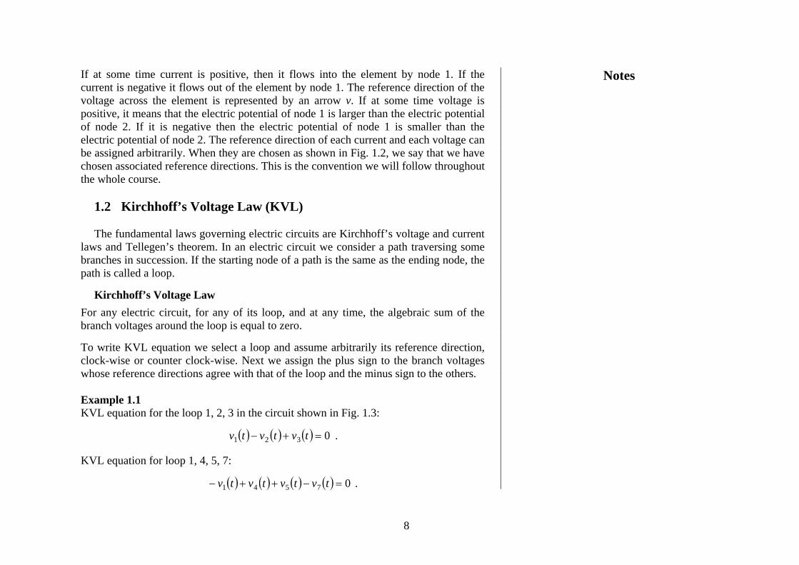
If at some time current is positive, then it flows into the element by node 1. If the current is negative it flows out of the element by node 1. The reference direction of the voltage across the element is represented by an arrow v. If at some time voltage is positive, it means that the electric potential of node 1 is larger than the electric potential of node 2. If it is negative then the electric potential of node 1 is smaller than the electric potential of node 2. The reference direction of each current and each voltage can be assigned arbitrarily. When they are chosen as shown in Fig. 1.2, we say that we have chosen associated reference directions. This is the convention we will follow throughout the whole course.
1.2 Kirchhoff’s Voltage Law (KVL) The fundamental laws governing electric circuits are Kirchhoff’s voltage and current
laws and Tellegen’s theorem. In an electric circuit we consider a path traversing some branches in succession. If the starting node of a path is the same as the ending node, the path is called a loop.
Kirchhoff’s Voltage Law
For any electric circuit, for any of its loop, and at any time, the algebraic sum of the branch voltages around the loop is equal to zero. To write KVL equation we select a loop and assume arbitrarily its reference direction, clock-wise or counter clock-wise. Next we assign the plus sign to the branch voltages whose reference directions agree with that of the loop and the minus sign to the others. Example 1.1 KVL equation for the loop 1, 2, 3 in the circuit shown in Fig. 1.3:
( ) ( ) ( ) 0321 =+− tvtvtv . KVL equation for loop 1, 4, 5, 7:
( ) ( ) ( ) ( ) 07541 =−++− tvtvtvtv .
Notes
8

v6(t)
v3(t)
v2(t)
v1(t) v4(t)
v5(t)
v7(t)
Fig. 1.3. An example circuit for illustrating KVL
KVL can also be expressed in terms of voltages between nodes creating a closed node sequence. A node sequence is called a closed node sequence if it starts and ends at the some node. Kirchhoff’s Voltage Law (general version)
For any electric circuit, for any closed node sequence, and for any time, the algebraic sum of all node-to-node voltages around the chosen closed node sequence is equal to zero. Example 1.2
64 5
3 2 1
v6 v3
v2 v1
v4
v5 v2,5
Fig. 1.4. An example circuit for illustrating KVL
Notes
9

Let us consider closed node sequences: 1, 2, 5, 4, 1 and 1, 2, 3, 6, 5, 4, 1. KVL equations: 1, 2, 5, 4, 1: 013522 =++−− vvvv , . 1, 2, 3, 6, 5, 4, 1: 0135642 =++−++− vvvvvv .
1.3 Kirchhoff’s Current Law (KCL) Another fundamental law governing electric circuits is Kirchhoff’s Current Law, as follows.
For any electric circuit, for any of its nodes, and at any time the algebraic sum of all the branch currents meeting at the node is zero. In the algebraic sum we assign the plus sign to the currents leaving the node and the minus sign to the currents entering the node. Example 1.3
3
2 1
i3(t)
i 2(t)
i 1(t)
i 4(t)
Fig. 1.5. An example circuit for illustrating KCL
1: ( ) ( ) ( ) 0321 =+− tititi , or simply 0321 =+− iii .
3: 043 =−− ii .
Notes
10

To formulate KCL in a more general form we consider gaussian surface defined as a balloon-like closed surface, as illustrated in Fig. 1.6.
the gaussian surface
i2
i3
i1
Fig. 1.6. The gaussian surface
KCL (general version) For all circuits, for all gaussian surfaces, for all times t, the algebraic sum of all currents crossing the gaussian surface at time t is equal to zero. In the algebraic sum we assign the plus sign to the currents leaving the gaussian surface and the minus sign to the currents entering the surface. Example 1.4 In the circuit shown in Fig. 1.6 we write KCL equation
0321 =−+− iii .
The topological properties of a circuit can be exhibited using a graph obtained by replacing each branch by a line. Each branch of the graph has orientation indicated by an arrow on the branch. This arrow is the same as the reference direction of the current flowing through the corresponding branch of the circuit. Thus, the graph can be used to write KVL and KCL equations.
Notes
11

1.4 Independence of KCL equations
For a given circuit we can write many KCL equations. Hence, the question arises how many of them are linearly independent.
4 3
11
3
2
2
Fig. 1.7. An example graph
To answer this question we consider the graph shown in Fig. 1.7 and write KCL equations at each node
0321 =−− iii ,
0421 =++− iii ,
043 =− ii .
If we add the first two equations together, we obtain
043 =+− ii .
Multiplying both sides of this equation by ( )1− yields
043 =− ii ,
which is exactly the third equation.
Notes
12

It means that the third equation is a linear combination of the first two equations. Thus, not each equation brings new information not contained in the others and at least one equation repeats the information contained in the others. However, if we reject the third equation, then the remaining ones are linearly independent. Thus, the third equation is redundant, it is useless and can be discarded. Generally, the following independence property of KCL equations holds. For any graph with n nodes KCL equations for any ( ) of these nodes form a set of 1−n ( )1−n linearly independent equations.
1.5 Independence of KVL equations
Similarly as in the case of KCL equations the question arises how to write a set of linearly independent KVL equations. The simplest answer is as follows. We write KVL equations selecting the loops so that any equation contains at least one voltage that has not been included in any of the previous equations.
It can be shown that for a circuit having b branches and n nodes 1+− nb linearly independent equations can be formulated.
8
3
1 2
4
5
6
7
I
IV
IIIII
Fig. 1.8. A graph for illustrating independence of KVL equations
Example 1.5 Let us consider the graph shown in Fig. 1.8. In this graph we write linearly independent KVL equations using the provided rule. As a result we obtain the following set of equations
Notes
13

0271 =++ vvv ,
0432 =−−− vvv ,
0654 =++ vvv ,
0867 =++ vvv .
1.6 Tellegen’s theorem
Let us consider a graph having b branches and n nodes. Let us use the associated reference directions. Tellegen’s theorem
Let be any set of branch currents satisfying KCL at any node and let be any set of branch voltages satisfying KVL at any loop. Then it holds bi,,i,i …21
bv,,v,v …21
01
=∑=
b
kkk iv .
Note that the set of branch currents and the set of branch voltages are associated with the given graph but not necessarily with the same circuit. For example, let us consider the graph shown in Fig. 1.9 and two different circuits depicted in Figs 1.10 and 1.11 having this graph. Tellegen’s theorem enables us to write the following equations:
044332211 =+++ iviviviv ,
044332211 =+++ i~v~i~v~i~v~i~v~ ,
044332211 =+++ i~vi~vi~vi~v ,
044332211 =+++ iv~iv~iv~iv~ .
Notes
14

43
2
1
1
3
2
Fig. 1.9. A graph having three nodes and four branches
v1
v2
v4
i4
i1
i3
v3
i2
1v~
2v~
4v~4i~
1i~
3i~
3v~
2i~
Fig. 1.10. A circuit having the graph of Fig. 1.9 Fig. 1.11. A circuit having the graph of Fig. 1.9
Notes
15

2. Circuit elements
The components used to build electric circuits are called circuit elements. In this section we define simple two-terminal circuit elements: a resistor, independent voltage and current sources.
2.1 Resistors
An element is said to be a resistor if its voltage-current relation is of algebraic type.
This relation is represented graphically by a curve in iv − plane, called the characteristic of the resistor. Any resistor can be classified as linear or nonlinear.
A resistor is called linear if its characteristic is a straight line through the origin (see Fig. 2.1).
v
i0
Fig. 2.1. Characteristic of a linear resistor
It is described by the equation iRv = (2.1) or vGi = , (2.2)
Notes
16
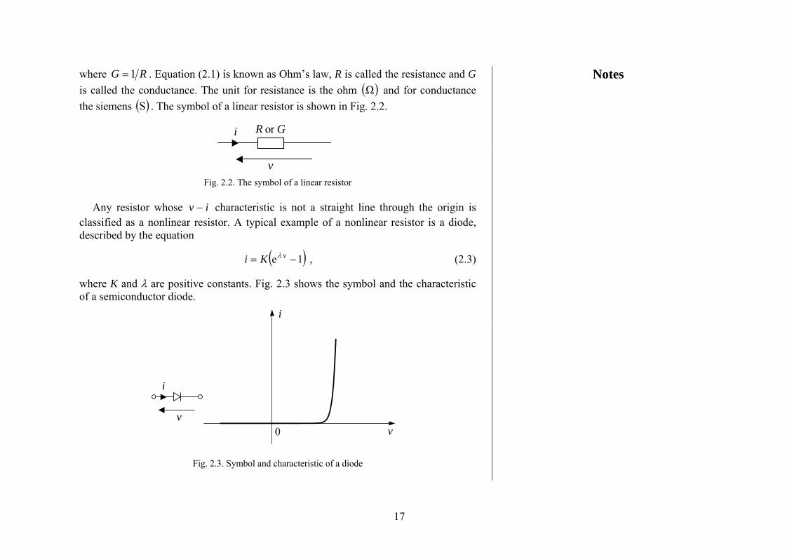
where RG 1= . Equation (2.1) is known as Ohm’s law, R is called the resistance and G is called the conductance. The unit for resistance is the ohm ( ) and for conductance the siemens
Ω( )S . The symbol of a linear resistor is shown in Fig. 2.2.
v
i R or G
Fig. 2.2. The symbol of a linear resistor
Any resistor whose characteristic is not a straight line through the origin is
classified as a nonlinear resistor. A typical example of a nonlinear resistor is a diode, described by the equation
iv −
( )1e −= vKi λ , (2.3)
where K and λ are positive constants. Fig. 2.3 shows the symbol and the characteristic of a semiconductor diode.
0 v
i
v
i
Fig. 2.3. Symbol and characteristic of a diode
Notes
17

A general symbol of any nonlinear resistor is depicted in Fig. 2.4.
v
i
Fig. 2.4. General symbol of a nonlinear resistor
2.2 Independent sources
Voltage source
An element is called a voltage source if it maintains a prescribed voltage ( )tvS between its terminals for any current flowing through the source. Consequently, a voltage source maintains a prescribed voltage ( )tv between its terminals in an arbitrary circuit to which it is connected.
S
The symbol of the voltage source is shown in Fig. 2.5. vS(t)
Fig. 2.5. The symbol of a voltage source
Generally, the prescribed voltage is a time varying signal ( )tvS . In a special case, it is constant , called a DC voltage source. In such a case, the characteristic expressing the voltage between the terminals of the source in terms of the current flowing through the source is a horizontal line, as shown in Fig. 2.6.
SV
VS
v
i 0
Fig. 2.6. Characteristic of a DC voltage source
Notes
18

The defined voltage source is an ideal element not encountered in the physical world. A real voltage source can be represented by an equivalent circuit shown in Fig. 2.7.
RS VS
Fig. 2.7. Model of a real voltage source
Certain devices have very small and can quite effectively be approximated by the ideal voltage source.
SR
Let us consider a real voltage source terminated by a load, as shown in Fig. 2.8.
i
SRvv
RS
VS Load
Fig. 2.8. A real voltage source terminated by a load
Using KVL and Ohm’s law we write the equation
iRVv SS −= , (2.4)
that describes, on the plane, the straight line, shown in Fig. 2.9. This line is a characteristic of the real voltage source, and is called a load line.
vi −
Notes
19

slope = -RS
RVS
v
i 0
VS
Fig. 2.9. Load line of a real voltage source
Current source
A current source is an element which maintains a prescribed current ( )tiS for any voltage ( ) between its terminals. Consequently, a current source maintains a prescribed current ( ) in an arbitrary circuit to which it is connected. The symbol of a current source is shown in Fig. 2.10.
tvtiS
iS (t)
Fig. 2.10. Symbol of a current source If the prescribed current is constant, ( ) SS Iti = the current source is called a DC current source. Its vi − characteristic is shown in Fig. 2.11.
Notes
20
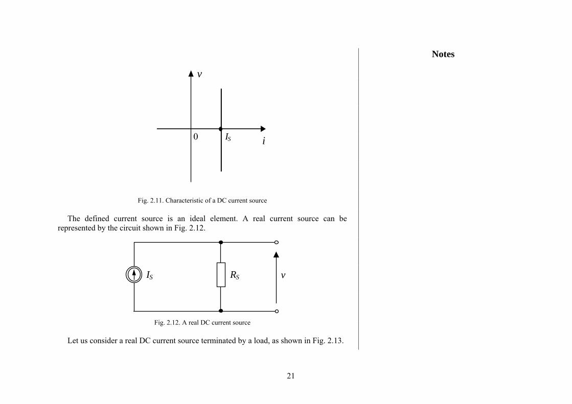
IS
v
i 0
Fig. 2.11. Characteristic of a DC current source
The defined current source is an ideal element. A real current source can be
represented by the circuit shown in Fig. 2.12.
vRSIS
Fig. 2.12. A real DC current source
Let us consider a real DC current source terminated by a load, as shown in Fig. 2.13.
Notes
21
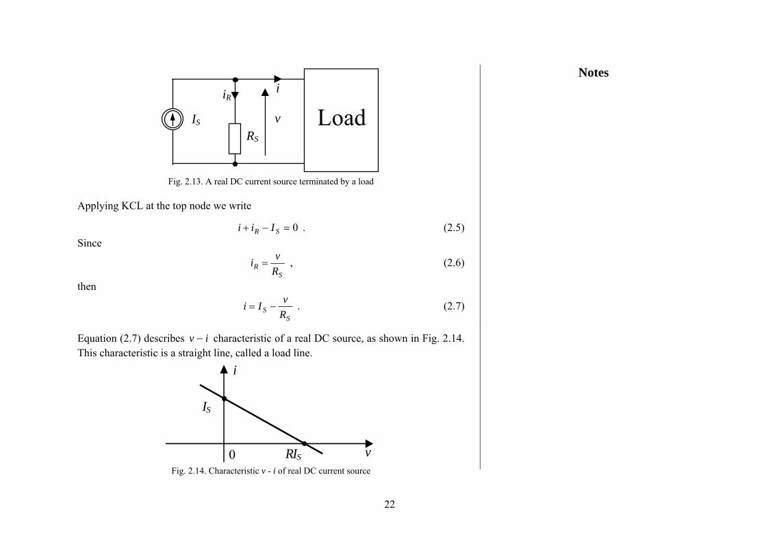
i
IS v
RS
iR
Load
Fig. 2.13. A real DC current source terminated by a load
Applying KCL at the top node we write
0=−+ SR Iii . (2.5) Since
S
R Rvi = , (2.6)
then
S
S RvIi −= . (2.7)
Equation (2.7) describes characteristic of a real DC source, as shown in Fig. 2.14. This characteristic is a straight line, called a load line.
iv −
RIS v
i
0
IS
Fig. 2.14. Characteristic v - i of real DC current source
Notes
22

Let us multiply both sides of equation (2.7) by and rearrange this equation as follows
SR
iRIRv SSS −= . (2.8)
By denoting SSS IRV = we obtain equation (2.4) that describes a real voltage source. Thus, if SSS IRV = , then the real current source and the real voltage source are equivalent.
Notes
23

3. Power and energy
Let us consider a circuit and draw two wires from this circuit. As a result we obtain a two-terminal circuit called a one-port. If the one-port is supplied with a source, the current ( )ti flows into the one-port by terminal A and the same current ( )ti flows out of the one-port by terminal B. Therefore, we indicate only one current ( )ti , as shown in Fig. 3.1. The voltage ( ) between the terminals is also indicated. tv
A
B
v(t)
i(t)
Fig. 3.1. A one-port with indicated the port voltage and port current
The current ( )ti and the voltage ( )tv are called a port current and a port voltage, respectively.
The instantaneous power entering the one-port is equal to the product of the port voltage and port current
( ) ( ) ( )titvtp = , (3.1)
where ( )tv is in volts, in amperes and ( )ti ( )tp in watts (abbreviated to W). tThe energy delivered to the one-port from time to is given by the equation 0t
, ( ) ( ) ( ) ( ) τττττ divdpt,twt
t
t
t∫∫ ==00
0
Notes
24

where a variable τ means time. Hence, it holds
( )tpdtdw
= .
If the one-port is a linear resistor, specified by R or G, then
( ) ( ) ( ) ( )tRititvtp 2== , (3.2)
( ) ( ) ( ) ( )tGvtitvtp 2== . (3.3) Thus, the instantaneous power is, in this case, nonnegative for all t.
ivIf the one-port is a nonlinear resistor, represented by a − characteristic located in the first and third quadrants only, then ( ) ( ) 0≥titv and the power entering the resistor is nonnegative, its energy is a nondecreasing function of time and the resistor consumes the energy. Such a resistor is called passive. If some parts of iv − characteristic lie in the second or third quadrant, then for some t, ( ) ( ) 0<titv , the power entering the resistor is negative and the resistor delivers energy to the outside world. Such a resistor is called active.
Notes
25

4. Simple linear resistive circuits
Circuits consisting of resistors and sources are classified as resistive circuits. In particular, they can be supplied with DC sources only. The analysis of such a class of circuits is called DC analysis.
Let us consider a circuit consisting of two linear resistors connected in series, as shown in Fig. 4.1.
R2R1
v2v1
i
v Fig. 4.1. Two resistors connected in series
To analyse this circuit we apply the KVL and Ohm’s law. Since the same current traverses both resistors we write
( )iRRiRiRvvv 212121 +=+=+= . (4.1) Hence, we have
21 RRiv
+= . (4.2)
Equation (4.2) states that the series connection of two linear resistors is equivalent to resistor R,
21 RRR += . (4.3)
Voltages across the resistors are specified by the equations:
vRR
RiRv21
111 +== , v
RRRiRv
21
222 +== .
Notes
26

Hence, it follows the relation
2
1
2
1
RR
vv
= , (4.4)
which states that the series connection of resistors and can be considered as a voltage divider. The voltage v is divided in proportion to and . Formula (4.3) can be directly generalized to the series connection of n linear resistors,
1R 2R
1R 2R
nR,,R …1
nRRR ++= 1 . (4.5)
Figure 4.2 shows the circuit consisting of two linear resistors connected in parallel.
R2R1
i2i1i
v
Fig. 4.2. Two resistors connected in parallel
Voltages across resistors and are identical and equal to v. The current i according to KCL satisfies the equation:
1R 2R
21 iii += . (4.6) Using Ohm’s law
1
1 Rvi = ,
22 R
vi = (4.7)
Notes
27
we obtain
vRR
i ⎟⎟⎠
⎞⎜⎜⎝
⎛+=
21
11 , (4.8)
or
iRv = (4.9) where
21
21
21
111
RRRR
RR
R+
=+
= . (4.10)
Thus, two resistors connected in parallel are equivalent to the resistor R specified by (4.10).
Using (4.7), (4.9), and (4.10) we write
iRR
RRvi
21
2
11 +
== , iRR
RRvi
21
1
22 +
== .
Hence, it holds
1
2
2
1
RR
ii= . (4.11)
Thus, the parallel connection of resistors and can be considered as a current divider, where the currents are divided according to equation (4.11).
1R 2R
Equation (4.10) can be directly generalised to the circuit consisting of n resistors connected in parallel nR,,R …1
nRR
R11
1
1++
= . (4.12)
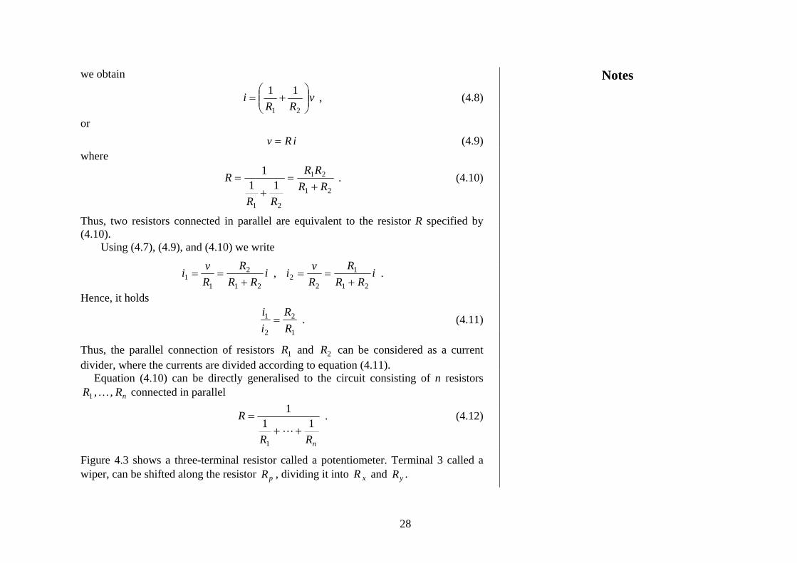
Figure 4.3 shows a three-terminal resistor called a potentiometer. Terminal 3 called a wiper, can be shifted along the resistor , dividing it into and . pR xR yR
Notes
28

RpRx
Ry3
R vy
i
V RpRx
Ry
Fig. 4.3. A potentiometer Fig. 4.4. Circuit containing a potentiometer
Let us consider the circuit shown in Fig. 4.4, containing a potentiometer. The circuit can be considered as a series connection of resistor and parallel connected resistors
and xR
yR R . Hence, the resistance faced by the voltage source is
RR
RRRR
y
yx ++= . (4.12)
Formula (4.12) enables us to find the current i
RRRR
R
vi
y
yx ++
= (4.13)
and then voltage yv
( ) vRRRRR
RRRR
RRiv
yyx
y
y
yy ++
=+
= . (4.14)
Notes
29

5. Resistive circuits. DC analysis
In this section we study circuits consisting of linear resistors and independent DC sources. We formulate some theorems governing these circuits, which enables us to analyse them efficiently.
5.1 Superposition theorem and its application Let us consider a linear circuit driven by n voltage sources
nSSS V,,V,V …21
, and m current sources
mSSS I,,I,I …21
.
The superposition theorem states that any branch current and any branch voltage in this circuit is given by the expression of the form
mn SmSSSnSS IkIkIkVhVhVh +++++++
2121 2121 , (5.1)
where coefficients and ( )n,,jh j …1= ( )m,,jk j …1= are constants and depend only on circuit parameters.
In other words, any branch current and any branch voltage is a linear combination of the voltage and current sources. Example 5.1 Let us consider a circuit consisting of linear resistors, a single voltage source and a single current source. We extract from this circuit the sources and an arbitrary resistor, as shown in Fig. 5.1. We wish to find the current i flowing through resistor R using the superposition theorem.
Notes
30

IS
i
RVS
Fig. 5.1. A circuit with extracted sources and a resistor
According to the superposition theorem
SS kIhVi += . (5.2)
Let and ShVi~ = SkIi~~ = , then
i~~i~i += . (5.3)
Note that if and i~i = 0=SI i~~i = if 0=SV .
If , then the branch containing the current source can be replaced by an open circuit (see Fig. 5.2). Thus, is the current flowing through resistor R in the circuit with the current source set to zero (removed). If 0
0=SIi~
=SV , then the branch containing the
voltage source can be replaced by a short circuit (see Fig. 5.3). Thus, i~~ is the current
flowing through resistor R in the circuit with the voltage source set to zero (short-circuited). The current can be regarded as a response of the circuit due to the voltage source acting alone. The current
i~
SV i~~ can be considered a response of the circuit due
to the current source acting alone. SI
Notes
31

i~
IS=0
R
VS
i~~
IS
R
VS=0
Fig. 5.2. The circuit shown in Fig. 5.1 driven Fig. 5.3. The circuit shown in Fig. 5.1. driven
by the voltage source VS by the current source IS
Generally, the response of the circuit due to several voltage and current sources is equal to the sum of the responses due to each source acting alone, that is with all other voltage sources replaced by short circuits and all other current sources replaced by open circuits. Example 5.2 Let us consider the circuit shown in Fig. 5.4, driven by a voltage source and a current source . We apply the superposition theorem to find voltage .
SV
SI 2v
R3
i2
v2R2IS
R1
VS
Fig. 5.4. A circuit driven by two sources
Notes
32

First we set the current source to zero. As a result, the circuit is driven only by the voltage source (see Fig. 5.5). SV
2i~
2v~
R3
R2
R1
VS
Fig. 5.5. Circuit of Fig. 5.4 driven only by the voltage source VS
In this circuit the same current 2i
~ traverses all the resistors. Hence, we find
321
2 RRRV
i~ S
++= ,
whereas the voltage 2v~ is, according to Ohm’s law, given by the equation
SvRRR
Ri~Rv~321
2222 ++== .
Now we set the voltage source to zero, obtaining the circuit shown in Fig. 5.6. SV
2i~~
2v~~
R3
R2IS
R1
Fig. 5.6. Circuit of Fig. 5.4 driven only by the current source IS
Notes
33

In this circuit the resistance faced by the current source equals
( )231
231
RRRRRR
+++
.
The product of this resistance and the current is voltage SI 2v~~
( )
SIRRRRRR
v~~231
2312 ++
+= .
The superposition theorem leads to the equation
( )SS I
RRRRRR
VRRR
Rv~~v~v
231
231
231
2222 ++
++
++=+= .
Notes
34

6. Three terminal resistive circuits
The three-terminal circuits shown in Figs 6.1 and 6.2 consist of three linear resistors. The circuit of Fig. 6.1 is called a Y circuit, whereas the one depicted in Fig. 6.2 is called a Δ circuit.
3Rv
1Rv2Rv
R1 R2
R3
i2
v2 i3
i1
v1
1
3
2
circuit
i2 i1 R12
R23R31
v2 v1
1
3
2
circuit
Fig. 6.1. Y circuit Fig. 6.2. Δ circuit
Notes
35

In a Y circuit it holds 213 iii += . (6.1) Hence, we find ( ) ( ) 23131213111 21
iRiRRiiRiRvvv RR ++=++=+= , (6.2) ( ) ( ) 23213213222 32
iRRiRiiRiRvvv RR ++=++=+= . (6.3)
To express and in terms of and in the Δ circuit, we apply current sources and to this circuit, as shown in Fig. 6.3.
1v 2v 1i 2i
1i 2i
i2 i1
R12
R23R31
v2 v1
1 2
3
Fig. 6.3. Δ circuit driven by two current sources
To find and we use the superposition theorem. First, we set current source to zero (see Fig. 6.4) and compute voltages
1v 2v 2i
1v~ and 2v~
Notes
36

( )
1231231
2312311 i
RRRRRR
v~+++
= , (6.4)
1231231
233123
2312
12 i
RRRRR
RRR
v~v~++
=+
= . (6.5)
i1
R12
R23R31
2v~v1
1 2
3
Fig. 6.4. The circuit shown in Fig. 6.3 with 02 =i
Next, we set current source to zero (see Fig. 6.5) and compute 1i 1v~~ and 2v~~
( )
2231231
3112232 i
RRRRRR
v~~+++
= , (6.6)
2311223
312331
3112
21 i
RRRRR
RRR
v~~v~~++
=+
= . (6.7)
Notes
37
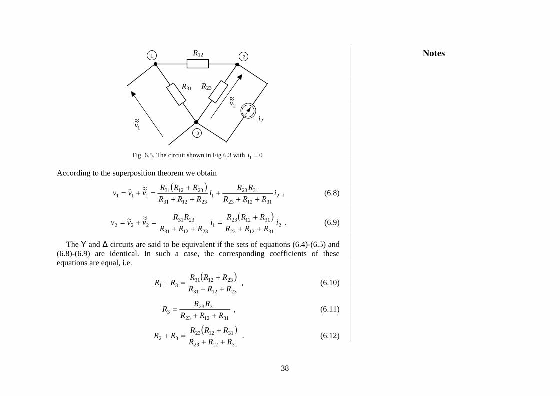
R12
R23R31
2v~~
1 2
3
i2 1v
~~
Fig. 6.5. The circuit shown in Fig 6.3 with 01 =i
According to the superposition theorem we obtain
( )
2311223
31231
231231
231231111 i
RRRRR
iRRR
RRRv~~v~v
+++
+++
=+= , (6.8)
( )
2311223
3112231
231231
2331222 i
RRRRRR
iRRR
RRv~~v~v
+++
=++
=+= . (6.9)
The Y and Δ circuits are said to be equivalent if the sets of equations (6.4)-(6.5) and (6.8)-(6.9) are identical. In such a case, the corresponding coefficients of these equations are equal, i.e.
( )
231231
23123131 RRR
RRRRR
+++
=+ , (6.10)
311223
31233 RRR
RRR
++= , (6.11)
( )
311223
31122332 RRR
RRRRR
+++
=+ . (6.12)
Notes
38

Solving this set of equations for , , we find 1R 2R 3R
312312
31121 RRR
RRR
++= , (6.13)
312312
23122 RRR
RRR
++= , (6.14)
312312
31233 RRR
RRR
++= . (6.15)
Formulas (6.13)-(6.15) give the resistances of the Y circuit which is equivalent to the Δ circuit. Solving the set of equations (6.12)-(6.14) for , , we find 12R 23R 31R
3
212112 R
RRRRR ++= , (6.16)
1
323223 R
RRRRR ++= , (6.17)
2
131331 R
RRRRR ++= . (6.18)
Formulas (6.16)-(6.18) give the resistances of the Δ circuit which is equivalent to the Y circuit.
The Y circuit is said to be balanced if YRRRR === 321 . Using in such a case, (6.16)-(6.18), we obtain ΔRRRR === 312312 , where YΔ RR 3= . (6.19)
Notes
39
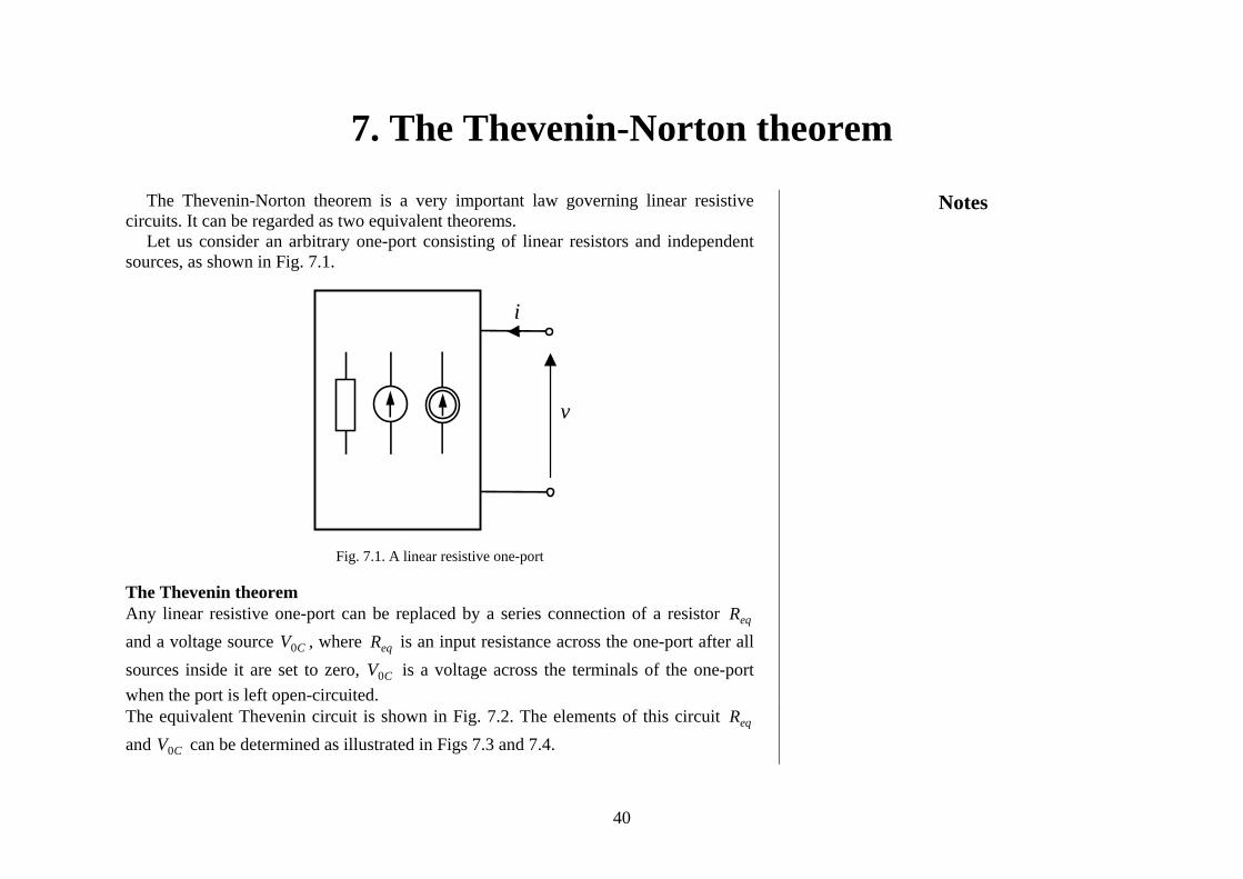
7. The Thevenin-Norton theorem
The Thevenin-Norton theorem is a very important law governing linear resistive circuits. It can be regarded as two equivalent theorems.
Let us consider an arbitrary one-port consisting of linear resistors and independent sources, as shown in Fig. 7.1.
v
i
Fig. 7.1. A linear resistive one-port The Thevenin theorem Any linear resistive one-port can be replaced by a series connection of a resistor and a voltage source , where is an input resistance across the one-port after all sources inside it are set to zero, is a voltage across the terminals of the one-port when the port is left open-circuited.
eqR
CV0 eqR
CV0
The equivalent Thevenin circuit is shown in Fig. 7.2. The elements of this circuit and can be determined as illustrated in Figs 7.3 and 7.4.
eqR
CV0
Notes
40

V0C
Req
v
i
Fig. 7.2. The Thevenin equivalent circuit
Req
i = 0
V0C
Fig. 7.3. Finding Req Fig. 7.4. Finding V0C
The Norton theorem Any linear resistive one-port can be replaced by a parallel connection of a linear resistor
and a current source . eqR SCI
eqR is defined as in the Thevenin theorem. is a current flowing through the short-circuited one-port.
SCI
Notes
41

The equivalent Norton circuit is shown in Fig. 7.5, whereas Fig. 7.6 shows the circuit enabling us to find . SCI
ISC Req v
i
ISC
i
Fig. 7.5. The equivalent Norton circuit Fig. 7.6. Finding Isc
The circuit shown in Fig. 7.6 can be replaced, on the basis of Thevenin’s theorem, by an equivalent circuit shown in Fig. 7.7.
V0C
Req ISC
Fig. 7.7. The circuit equivalent to the circuit of Fig. 7.6
Notes
42
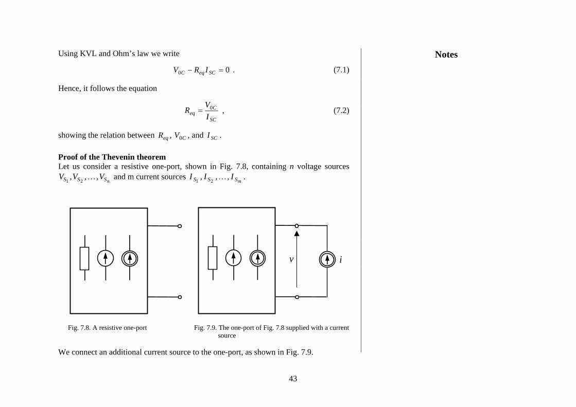
Using KVL and Ohm’s law we write
00 =− SCeqC IRV . (7.1) Hence, it follows the equation
SC
Ceq I
VR 0= , (7.2)
showing the relation between , , and . eqR CV0 SCI Proof of the Thevenin theorem Let us consider a resistive one-port, shown in Fig. 7.8, containing n voltage sources
and m current sources . nSSS V,,V,V …
21 mSSS I,,I,I …21
v i
Fig. 7.8. A resistive one-port Fig. 7.9. The one-port of Fig. 7.8 supplied with a current source
We connect an additional current source to the one-port, as shown in Fig. 7.9.
Notes
43

On the basis of the superposition theorem we obtain
. (7.3) ikIkVhv sj
m
jjsj
n
jj 0
11++= ∑∑
==
If , then the port terminals are open-circuited and 0=i CVv 0= . Hence, we have
. (7.4) sj
m
jjsj
n
jjC IkVhV ∑∑
==
+=11
0
If we set all the sources inside the one-port to zero, that is 021
====nSSS VVV … ,
021
====mSSS III … , then equation (7.3) reduces to
ikv 0= , (7.5) hence,
eqRivk ==0 (7.6)
and equation (7.3) can be rewritten in the form
iRVv eqC += 0 , (7.7)
where and are defined as in the Thevenin theorem. Equation (7.7) describes the circuit depicted in Fig. 7.8, being Thevenin’s equivalent circuit.
CV0 eqR
V0C
Req
v
i
Fig. 7.8. The Thevenin equivalent circuit
Notes
44

Note that the Thevenin circuit shown in Fig. 7.8 is equivalent to the circuit depicted in Fig. 7.9, being the Norton circuit. Thus, the Thevenin and Norton circuits are equivalent.
eq
C
RV0
eqR SCeq
C IRV
=0
Fig. 7.9. The circuit equivalent to the circuit shown in Fig. 7.8
Example Let us consider the one-port shown in Fig. 7.10.
E2
R2
E1
R1
V0C
Req
Fig. 7.10. An example one-port Fig. 7.11. Thevenin’s circuit The equivalent Thevenin circuit is shown in Fig. 7.11. We find the elements and
of this circuit. CV0
eqRAccording to Thevenin’s theorem is the input resistance of the one-port shown in Fig. 7.12.
eqR
Notes
45

R2R1
i
V0C
E2
R2
E1
R1
Fig. 7.12. A one-port enabling us Fig. 7.13. A circuit enabling us to find Req to find V0C
Hence, we have
21
21
RRRRReq +
= . (7.8)
To find we consider a circuit with open-circuited terminals shown in Fig. 7.13. In this circuit the same current i traverses all the elements. To find this current we apply KVL and Ohm’s law
CV0
21
21
RREEi
+−
= . (7.9)
Since the current flows through resistor , we have i 2R
21
2112
21
2122220 RR
RERERREEREiREV C +
+=
+−
+=+= . (7.10)
Notes
46

8. Node method
Kirchhoff’s laws and Ohm’s law enable us to analyse simple resistive circuits. However, such an approach is inefficient in the case of more complex circuits. In this Section we develop a general, very useful and commonly applied method, called the node method.
To explain this method we consider a circuit having nodes and introduce a concept of node-to-datum voltage. For this purpose we choose arbitrarily one of these nodes as a datum node. The potential of this node is set to zero, hence, it is grounded. For the remaining 1
n
−n nodes we introduce node-to-datum voltages (or simply node voltages) , between these nodes and the datum. The reference directions of the node
voltages are shown in Fig. 8.1. 11 −ne,,e …
e1
2
en-1e2
n-1 1
n
Fig. 8.1. Reference directions of the node voltages It is easy to see that voltage between any two nodes and k j can be expressed in terms of node voltages and . ke je
jkkj eev −= . (8.1)
Notes
47
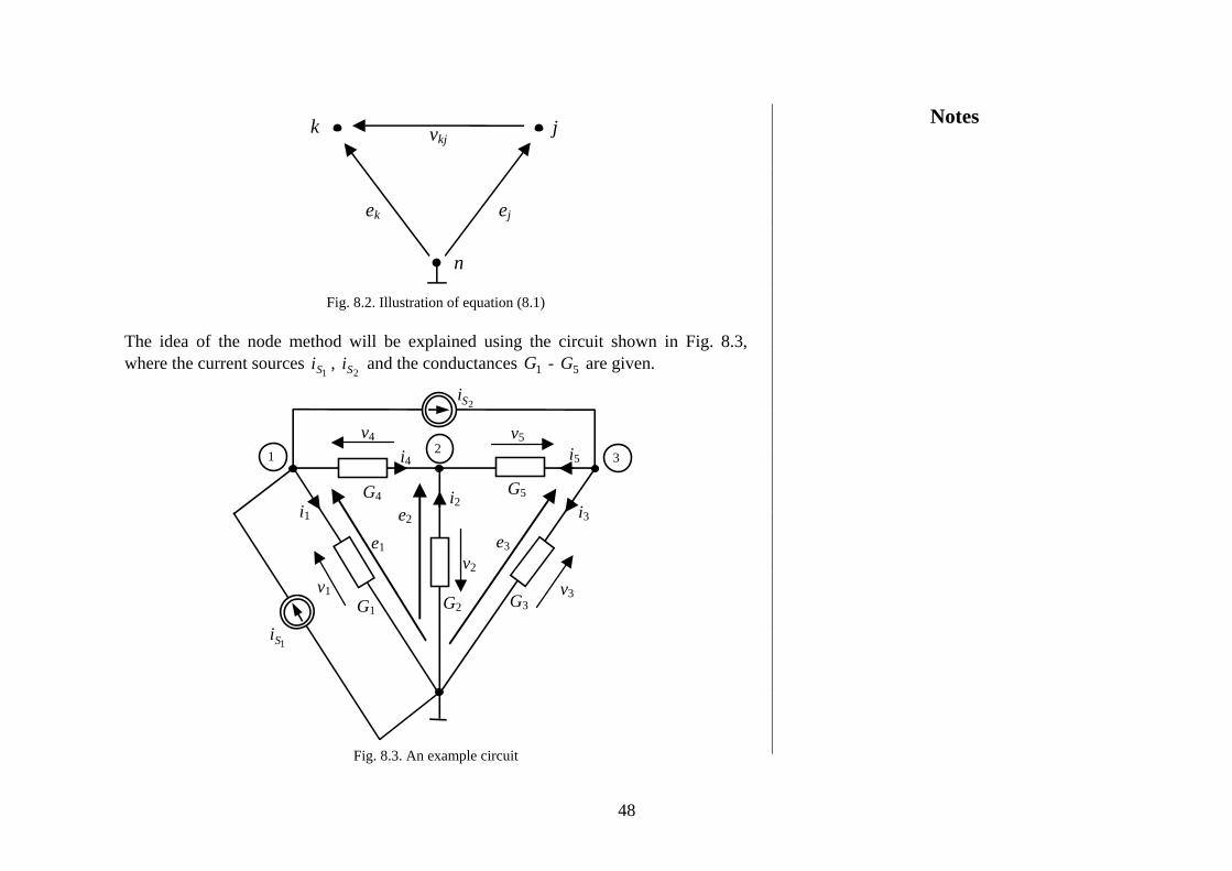
vkj
ek ej
j k
n
Fig. 8.2. Illustration of equation (8.1)
The idea of the node method will be explained using the circuit shown in Fig. 8.3, where the current sources , and the conductances - are given.
1Si 2Si 1G 5G
2Si
1Si
e3
G4
G3G2G1
i5i4
i3i2i1
v4
v3
v2
v1
v5
e2
e1
G5
1 2 3
Fig. 8.3. An example circuit
Notes
48

We choose the bottom node as a reference, introduce node voltages and write KCL equations at nodes 1, 2, 3 0
2141 =+−+ SS iiii ,
0542 =−−− iii , (8.2)
0253 =−+ Siii .
Next, we express the branch currents in terms of node voltages
( )
( )( ) ,eeGvGi
,eeGvGi,eGvGi
,eGeGvGi,eGvGi
235555
214444
33333
2222222
11111
−==−==
==−=−==
==
(8.3)
and substitute them into (8.2)
( )( ) ( )
( ) .ieeGeG,eeGeGeeG
,iieeGeG
S
SS
2
21
23533
23522214
21411
0=−+
=−−+−−
−=−+
(8.4)
Finally, we rearrange equations (8.4) as follows
( )( )( ) .ieGGeG
,eGeGGGeG
,iieGeGG
S
SS
2
21
35325
35252414
24141
0=++−
=−+++−
−=−+
(8.5)
The set of node equations (8.5) contains three unknowns , , . 1e 2e 3e
Notes
1 2
3
49

Let us replace the resistor by a voltage source , as shown in Fig. 8.4. 2G2SV
2Si
1Si
e3
G4
G3G1
i5i4
i3i2i1
v4
v3v1
v5
e2
e1
G5
1 2 3
2SV
Fig. 8.4. Circuit driven by current and voltage sources Equations written at node 1 and 3 are the same as in the previous case. Hence, we only need to write an equation at node 2. Since the current cannot be expressed in terms of the branch voltage, it is considered an additional variable. Thus, we obtain the following set of equations
2i
( )( ) ( )
( ) .ieeGeG,eeGieeG
,iieeGeG
S
SS
2
21
23533
2352214
21411
0=−+
=−−+−−
−=−+
(8.6)
Notes
1
2
3
50

This is a set of three equations with four unknown variables , , , . Therefore, we add another equation of the form
1e 2e 3e 2i
22 SVe = , (8.7)
where is the given voltage source. Substituting (8.7) into (8.6) we eliminate the variable and obtain the set of three equations in three variables , ,
2SV
2e 1e 3e 2i
( )( ) ( )
( ) .iVeGeG
,VeGiVeG
,iiVeGeG
SS
SS
SSS
22
22
212
3533
35214
1411
0
=−+
=−−+−−
−=−+
(8.8)
2Si
1Si
e3
G4
G3G2G1
i5i4
i3i2i1
v4
v3
v2
v1
v5
e2
e1
1 2 3
Fig. 8.5. Nonlinear resistor circuit
Notes 1
2
3
51

The node method can be also applied to circuits containing nonlinear resistors. It will be explained via an example circuit shown in Fig. 8.5, including a nonlinear resistor (semiconductor diode) described by the equation
( )155 −= veKi λ . (8.9)
To write the node equations we introduce temporarily the current as an additional variable
5i
( )( )
.iieG,ieGeeG
,iieeGeG
S
SS
2
21
533
522214
21411
0=+=−+−−
−=−+
(8.10)
Next we express in terms of the corresponding node voltages 5i
( ) ( )( )11 2355 −=−= −eev eKeKi λλ (8.11)
and substitute it into (8.10)
( )( ) ( )( )
( )( ) .ieKeG
,eKeGeeG
,iiveGeG
See
ee
SSS
223
23
212
1
01
33
22214
1411
=−+
=−−+−−
−=−+
−
−
λ
λ (8.12)
In this way, we obtain a set of three node equations, in three unknown variables, describing the nonlinear circuit shown in Fig. 8.5.
Notes
1
2
3
1
2
3
52

9. Simple nonlinear circuits
In this section we analyse very simple circuits consisting of nonlinear resistors by means of a graphical approach.
Series connection of resistors Figure 9.1 shows a circuit consisting of two nonlinear resistors connected in series.
i2
i1
v2
v1
i
v
Fig. 9.1. Two nonlinear resistors connected in series The resistors are specified by their characteristics depicted in Figs 9.2 and 9.3.
i1
v1
1
i2
v2
2
Fig. 9.2. The characteristic i1 – v1 Fig. 9.3. The characteristic i2 – v2
Notes
53

On the basis of KVL we write
21 vvv += . (9.1) Since the resistors are connected in series, the same current traverses each of them, hence, it holds
iii == 21 . (9.2)
On the basis of these equations we can find the characteristic vi − using a graphical approach. To trace the characteristic we add the voltages and specified by the characteristics
1v 2v
1vi − and , respectively, for each value of the current . 2vi − iThe graphical construction is illustrated in Fig. 9.4.
0 i
v2 v = v1+v2
v1
i
v1, v2, v
1
2
Fig. 9.4. Graphical construction for finding characteristic i-v
Parallel connection of resistors Figure 9.5. shows a circuit consisting of two nonlinear resistors connected in parallel.
Notes
54
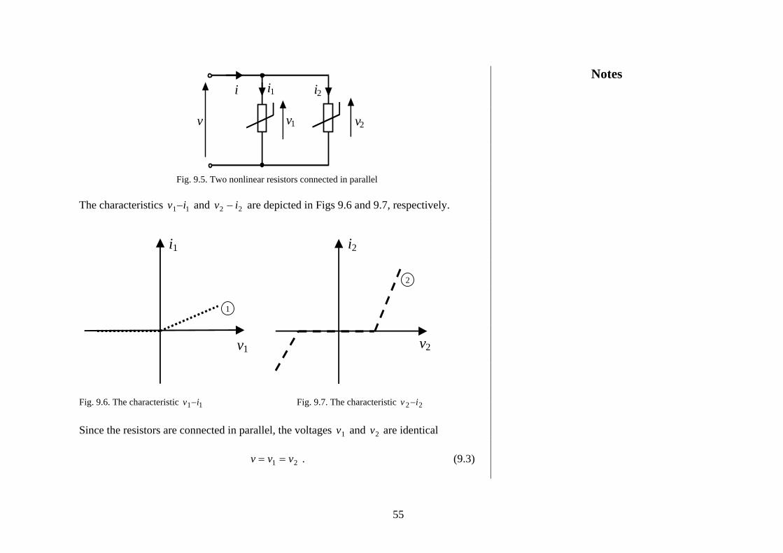
i1 i2
v1 v2
i
v
Fig. 9.5. Two nonlinear resistors connected in parallel
The characteristics and are depicted in Figs 9.6 and 9.7, respectively. 11 iv − 22 iv −
v1
i1
1
i2
v2
2
Fig. 9.6. The characteristic Fig. 9.7. The characteristic 11 iv − 22 iv − Since the resistors are connected in parallel, the voltages and are identical 1v 2v 21 vvv == . (9.3)
Notes
55

Using KCL at the top node we have
21 iii += . (9.4)
Thus, the characteristic iv − can be traced in a graphical manner by adding for each value of v the corresponding currents and (see Fig. 9.8). 1i 2i
i
i1 = i2
0 v
i1, i2, i
v
2
1
Fig. 9.8. Graphical construction for finding characteristic v-i
Operating points
Nonlinear circuits driven by DC sources have constant solutions (branch voltages and current), called operating points. The basic question of the analysis of this class of circuits is finding the operating points. If a circuit is simple, the operating point can be found using a graphical approach, To illustrate this approach we consider a typical biasing circuit depicted in Fig. 9.9, including a nonlinear resistor specified by the characteristic shown in Fig. 9.10. The linear part of this circuit, consisting of the DC voltage source E and resistor R , is described by the equation
bb RiEv += . (9.5)
Notes
56

B
ia
va
ib A
Rv
vb
R
E
0
va=f(ia)
ia
Fig. 9.9. Typical biasing circuit Fig. 9.10. Characteristic of the nonlinear resistor belonging to the circuit of Fig. 9.9 We transcribe this characteristic in the bb vi − plane to the aa vi − plane. Since
ab vv = and ab ii −= , we obtain aa RiEv −= . (9.6) Equation (9.6) describes a straight line, shown in Fig. 9.11. On the same plane we plot the characteristic
( )aa ifv = .
The point of intersection ( )aa v,i is the solution of the set of equations
( )aa ifv = ,
aa RiEv −= , hence, the intersection is the operating point of the circuit shown in Fig. 9.9.
Notes
57

REai
av
E
0
va
ia
Fig. 9.11. Graphical construction for finding the operation point
Notes
58

10. Controlled sources
Controlled sources are circuit elements very useful in the modeling of electronic devices. A controlled source is a two-port consisting of two branches. A primary branch is either a short circuit or an open circuit. A secondary branch is either a voltage source or a current source. The source waveform depends on a voltage or a current of the primary branch. Thus, there are four types of controlled sources. The controlled sources can be classified as linear or nonlinear. All the controlled sources are shown in Figs 10.1 – 10.4.
1i
2i
2v1ir
01 =v
a)
1i
2i
2v( )1ifr 01 =v
b)
Fig. 10.1. Current-controlled voltage sources (CCVS) a) linear, b) nonlinear
a)
2i
2v1gv
01 =i
1v
2i
2v( )1vfg
01 =i
1v
b)
Fig. 10.2. Voltage-controlled current sources a) linear, b) nonlinear
Notes
59

1i
a)
2i
2v1iα
01 =v
1i
2i
2v ( )1ifα
01 =v
b)
Fig. 10.3. Current-controlled current sources a) linear, b) nonlinear
a)
1vμ
2i
2v1v
01 =i
b)
2i
2v( )1vfμ1v
01 =i
Fig. 10.4. Voltage-controlled voltage sources a) linear, b) nonlinear
Controlled sources are very useful in modeling electronic devices. For example the Ebers-Moll model of an npn bipolar transistor contains two linear current controlled current sources, as illustrated in Fig. 10.5.
iC
iF iR
iE
iB
BE CvBE vBC
αF iF αR iR
Fig. 10.5. The Ebers-Moll model of an npn bipolar transistor
Notes
60

11. Capacitor
11.1 Introduction
A capacitor is a two-terminal element which stores an electric charge. The simplest example of a capacitor is shown in Fig. 11.1. It is made of two flat parallel metal plates in free space.
-q(t)
q(t) i(t)
d
v(t)
Fig. 11.1. Parallel plate capacitor When a current ( )ti is applied, then a charge ( ) ( )tCvtq = is induced on the upper plate and an equal but opposite charge is induced on the lower plate. The constant of proportionality, called capacitance, is given approximately by
d
AC 0ε= ,
Notes
61

where
mF10
361 9
0−=
πε
is the dielectric constant called permittivity, A is the plate area and is the separation of the plates. The units of capacitance are farads, abbreviated to F.
d
Equation
Cvq = (11.1)
defines the qv − characteristic of the capacitor. The characteristic is a straight line through the origin with a slope C , as shown in Fig. 11.2.
v
q
Fig. 11.2. Characteristic v-q of a linear capacitor
A capacitor whose characteristic is a straight line through the origin is called a linear capacitor. Otherwise, the capacitor is said to be nonlinear. An example qv − characteristic of a nonlinear capacitor is shown in Fig 11.3.
Notes
62

v
q
Fig. 11.3. Characteristic v-q of a nonlinear capacitor
The symbols of a linear and a nonlinear capacitor and the reference directions of ( )ti and ( ) are shown in Figs 11.4 and 11.5. In these figures q is the charge on this plate which is pointed by the reference arrow of the current i .
tv
v(t)
i(t) q(t)
C
q(t)
v(t)
i(t)
Fig. 11.4. Symbol of a linear capacitor Fig. 11.5. Symbol of a nonlinear capacitor
Notes
63

The current ( )ti is given by the equation
( ) ( )ttqti
dd
= . (11.2)
Using equation (11.1) and (11.2) we obtain
( )tvC
tCv
tqi
dd
dd
dd
=== . (11.3)
Equation (11.3) expresses capacitor current in terms of capacitor voltage. To express capacitor voltage in terms of capacitor current we replace the variable t with τ obtaining
( ) ( )τττ
ddvCi = . (11.4)
Next we integrate both sides of (11.4) between and 0 t
( ) ( )( )
( )( ))0()(dd
ddd
000
vtvCvCvCitv
v
tt
−=== ∫∫∫ τττττ .
Hence, it holds
( ) ( ) ( ) ττ diC
vtvt
∫+=0
10 . (11.5)
11.2 Continuity property
Let us replace in equation (11.5) by t tt d+
( ) ( ) ( ) ττ d10dd
0∫+
+=+tt
iC
vttv (11.6)
and assume that ( )ti is bounded for all , that is there exists a constant t L , such that ( ) Lti < for all . t
Notes
64

Subtracting equation (11.5) from (11.6) we have
( ) ( ) ( ) ττ d1dd
0∫+
=−+tt
iC
tvttv . (11.7)
As , then , hence, 0d →t ( ) 0dd
0
→∫+
ττtt
i ( ) ( )tvttv →+ d .
Thus, voltage across any linear capacitor is a continuous function of time. It means that this voltage cannot jump instantaneously from one value to another.
11.3 Energy stored in a capacitor
Consider a capacitor supplied with a generator as shown in Fig. 11.6.
v(t)
i(t)
C Generator
Fig. 11.6. A capacitor supplied with a generator
The energy delivered by the generator to the capacitor from time to is given by the equation
0t t
, (11.8) ( ) ( ) ( ) ( ) τττττ dd00
0 ivpt,tAt
t
t
t∫∫ ==
where is the instantaneous power entering the capacitor. p
Notes
65
Let ( ) 00 =tv , hence, no charge is stored in the capacitor. We choose this state as the state corresponding to zero energy, i.e. ( ) 00 =tw , where at 0tt = is the initial energy of the capacitor. Let us replace t by another variable τ in equation (11.3)
( ) ( )τττ
ddvCi =
and rewrite it in the form ( ) vCi dd =ττ . (11.9)
Substituting (11.9) into (11.8) yields
( ) ( ) ( )( ) ( )
( )20
2
00 )(
21
21dd
0
tvCvCvvCivt,tAtvtvt
t
==== ∫∫ τττ . (11.10)
A capacitor is an element that stores energy, but does not dissipate it. Hence, the energy stored in the capacitor at time t is given by the equation
( ) ( ) ( ) ( )t,tAt,tAtwtw 000 =+= . (11.11)
Since ( ) 00 =tw and is specified by (11.10), we have ( )t,tA 0
( ) ( )tCvtw 2
21
= . (11.12)
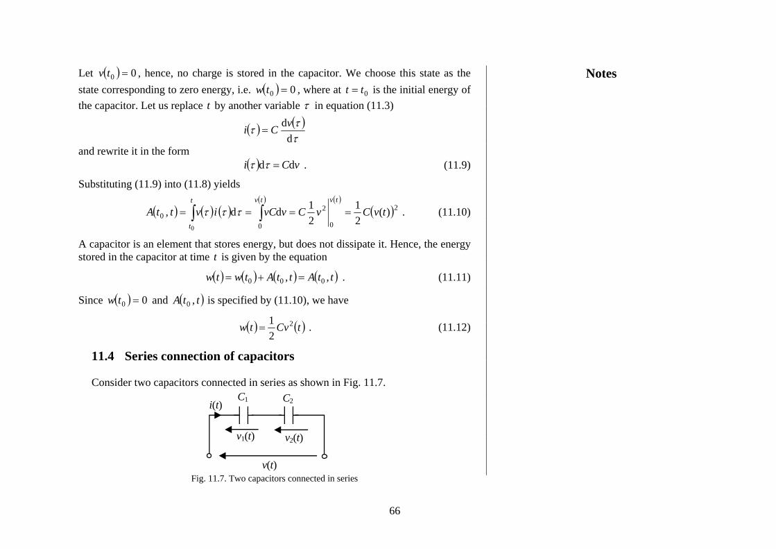
11.4 Series connection of capacitors
Consider two capacitors connected in series as shown in Fig. 11.7.
i(t)
v2(t)
C2
v1(t)
C1
v(t) Fig. 11.7. Two capacitors connected in series
Notes
66

Since the same current traverses both capacitors we write, on the basis of (11.5)
( ) ( ) ( ) ττ d1001
11 ∫+=t
iC
vtv , (11.13)
( ) ( ) ( ) ττ d1002
22 ∫+=t
iC
vtv . (11.14)
Using KVL yields
( ) ( ) ( )tvtvtv 21 += . (11.15)
At equation (11.15) becomes 0=t
( ) ( ) ( )000 21 vvv += . (11.16)
We add equations (11.13) and (11.14) together and apply (11.16)
( ) ( ) ( ) ττ d110021∫⎟⎟⎠
⎞⎜⎜⎝
⎛++=
t
iCC
vtv . (11.17)
Let
CCC111
21=+ , (11.18)
then
( ) ( ) ( ) ττ d100∫+=t
iC
vtv . (11.19)
Equation (11.19) describes the equivalent capacitor of two capacitors connected in series. The initial voltage of this capacitor is specified by (11.16), whereas the capacitance is given by (11.18).
Notes
67

11.5 Parallel connection of capacitors
Figure 11.8 shows two capacitors connected in parallel. Since voltages across the capacitors are identical, both capacitors have the same initial voltage ( )0v .
C1
i2(t) i1(t) i(t)
C2 v(t)
Fig. 11.8. Two capacitors connected in parallel
Currents flowing through the capacitors are given by the equations
( ) ( )ttvCti
dd
11 = , ( ) ( )ttvCti
dd
22 = .
Applying KCL at the top node and the above equations yields
( ) ( ) ( ) ( ) ( ) ( )ttvC
ttvCCtititi
dd
dd
2121 =+=+= ,
where
21 CCC += . (11.20)
Formula (11.20) gives the capacitance of the equivalent capacitor.
Notes
68

12. Inductor
12.1 Introduction
Figure 12.1 shows an inductor made of wire wound around a core, made of a nonmetallic material.
φ i(t)
v(t)
Fig. 12.1. An example inductor When the device is supplied with a time varying current source, a magnetic flux is induced and circulates inside the core. The magnetic flux linkage ( )tφ , being the total flux linked by all turns of the coil, is proportional to the current
( ) ( )tLit =φ , (12.1) where the coefficient L is called inductance. The units of magnetic flux are webers (W), the units of inductance are henrys (H).
Notes
69

If the core shown in Fig. 12.1 is a toroid made of material having the magnetic constant (permeability) 0μ , then the inductance is given by the formula
l
ANL2
0μ= , (12.2)
where mH104 4
0−⋅= πμ , is the number of turns, N A is the cross-sectional area of the
core, is the midcircumference along the core. lThe equation
Li=φ (12.3)
defines φ−i characteristic of the inductor. The characteristic is a straight line through the origin with a slope equal to L (see Fig. 12.2). In such a case the inductor is classified as linear.
0
slope = L
i
φ
Fig. 12.2. Characteristic of a linear inductor
Otherwise, if the characteristic is not a straight line through the origin, the inductor is called nonlinear. The typical characteristic of a nonlinear inductor is shown in Fig. 12.3.
Notes
70

0 i
φ
Fig. 12.3. Characteristic of a nonlinear inductor
The symbols of linear and nonlinear inductors are shown in Fig. 12.4.
v(t)
i(t)
L v(t)
i(t)
Fig. 12.4. Symbols of linear and nonlinear inductors
According to Faraday’s induction law
( ) ( )tttv
ddφ
= . (12.4)
Notes
71

Substituting (12.3) into (12.4) yields
( )tiLLi
tv
dd
dd
== . (12.5)
To express the current flowing through a linear inductor in terms of the voltage across the inductor we replace t with
i vτ and rewrite equation (12.5) in the form
( ) ( )τττ
ddiLv = . (12.6)
Next we integrate both sides of equation (12.6) between and 0 t
( ) ( )( )
( )( ))0()(dd
ddd
000
itiLiLiLvti
i
tt
−=== ∫∫∫ τττττ .
Hence, we have
( ) ( ) ( ) ττ d100∫+=t
vL
iti . (12.7)
12.2 Continuity property
Let us replace in equation (12.7) by t tt d+
( ) ( ) ( ) ττ d10dd
0∫+
+=+tt
vL
itti (12.8)
and assume that ( )tv is bounded for all , that is, there exists a constant t M such that ( ) Mtv < for all . Subtracting equation (12.7) from (12.8) yields t
( ) ( ) ( ) ( ) ( ) ττττττ d1dd1dd
0
d
0∫∫∫++
=⎟⎟⎠
⎞⎜⎜⎝
⎛−=−+
tt
t
ttt
vL
vvL
titti .
Notes
72

Since ( ) 0d1 d→∫
+ tt
tv
Lττ as , then 0d →t ( ) ( )titti →+ d . Thus, current flowing through
any linear inductor is a continuous function of time. This means that inductor current cannot jump instantaneously from one value to another.
12.3 Hysteresis
Ferromagnetic core inductors exhibit the hysteresis phenomenon as depicted in Fig. 12.5.
1
2
3
i2
i3 i4 i1 i
φ3
φ1
φ
Fig. 12.5. Hysteresis phenomenon
The characteristic shown in Fig. 12.5 is obtained by increasing the current from to
, next decreasing this current from to and after that increasing from to . Thus, the flux decreases according to the upper branch 2 and increases according to the lower branch 3. As a result, a close curve is traced. The magnetic flux becomes zero for the negative value and the positive value of the current.
i 01i 1i 3i 3i 1i
2i 4i
Notes
73

12.4 Energy stored in an inductor
Consider an inductor supplied with a generator as shown in Fig. 12.6.
v(t)
i(t)
L Generator
Fig. 12.6. An inductor supplied with a generator
The energy delivered by the generator to the inductor from time to is given by the equation
0t t
, (12.9) ( ) ( ) ( ) ( ) τττττ dd00
0 ivpt,tAt
t
t
t∫∫ ==
where p is the instantaneous power entering the inductor. Let ( ) 00 =ti , consequently also the magnetic flux equals zero and no magnetic field exists in the inductor. Such a state can be considered a state corresponding to zero energy stored. Let us substitute (12.6) into (12.9). Then, we have
( ) ( ) ( )( )
( )
( )
( )( ))()(
21
21dd
dd
0222
0000
titiLLiiiLiiLt,tAti
ti
ti
ti
t
t
−==== ∫∫ ττττ .
Since ( ) 00 =ti the energy initially stored in the inductor is also equal to zero, ( ) 00 =tw and the energy delivered to the inductor from 0tt = to is t
( ) ( )tLit,tA 20 2
1= . (12.10)
Notes
74

An inductor is an element that stores energy, but does not dissipate it. Hence, the energy stored in the inductor at time t is given by the equation
( ) ( ) ( ) ( )tLit,tAtwtw 200 2
1=+= . (12.11)
12.5 Series connection of inductors
Consider two inductors connected in series as shown in Fig. 12.7.
i(t) v2(t)
L2
v1(t)
L1
v(t)
Fig. 12.7. Two inductors connected in series
Since identical currents flow through the inductors, both inductors have the same initial current ( )0i . KVL leads to the equation
( ) ( ) ( )tvtvtv 21 += , where
( ) ( )ttiLtv
dd
11 = , ( ) ( )ttiLtv
dd
22 = .
Hence, we have
( ) ( ) ( ) ( ) ( ) ( )ttiL
ttiLL
ttiL
ttiLtv
dd
dd
dd
dd
2121 =+=+= ,
where
21 LLL += . (12.12)
Formula (12.12) gives the inductance of the equivalent inductor.
Notes
75

12.6 Parallel connection of inductors
Figure 12.13 shows two inductors connected in parallel.
L1
i2(t) i1(t)
i(t)
L2 v(t)
Fig. 12.13. Two inductors connected in parallel
We write KCL equation
( ) ( ) ( )tititi 21 +=
and substitute into this equation
( ) ( ) ( ) ττ d1001
11 ∫+=t
vL
iti
and
( ) ( ) ( ) ττ d1002
22 ∫+=t
vL
iti .
As a result we obtain
( ) ( ) ( ) ττ d100∫⎟⎠⎞
⎜⎝⎛+=
t
vL
iti , (12.13)
where ( ) ( ) ( )000 21 iii += (12.14)
Notes
76

and
LLL111
21=+ (12.15)
or
21
21
LLLL
L+
= . (12.16)
Thus, the parallel connection of two inductors can be replaced by a single inductor having the inductance specified by (12.16), with the initial condition (12.14).
Notes
77
13. Operational-amplifier circuits
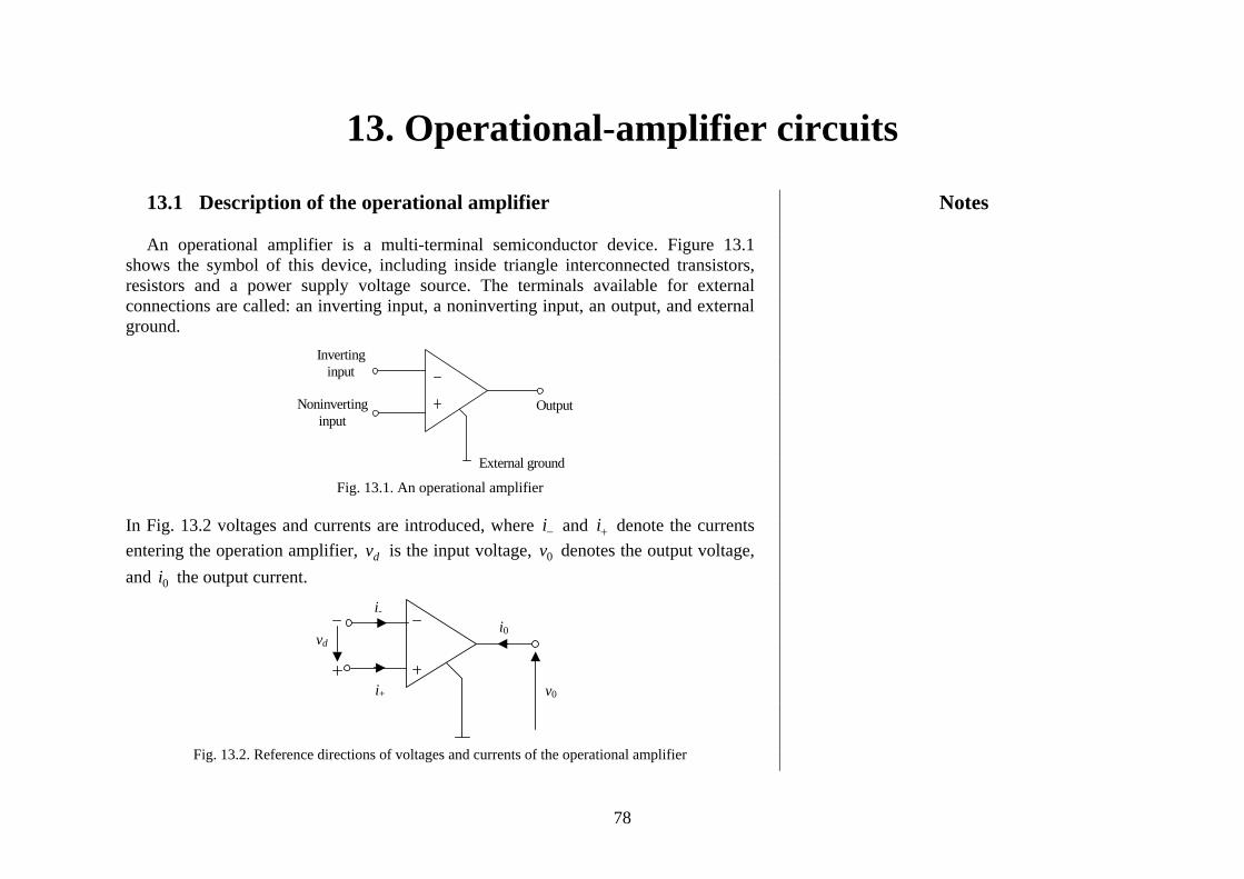
13.1 Description of the operational amplifier
An operational amplifier is a multi-terminal semiconductor device. Figure 13.1 shows the symbol of this device, including inside triangle interconnected transistors, resistors and a power supply voltage source. The terminals available for external connections are called: an inverting input, a noninverting input, an output, and external ground.
Noninvertinginput
Invertinginput
External ground
Output
Fig. 13.1. An operational amplifier
In Fig. 13.2 voltages and currents are introduced, where and denote the currents entering the operation amplifier, is the input voltage, denotes the output voltage, and the output current.
−i +i
dv 0v
0i
i+
i-
v0
vd i0
Fig. 13.2. Reference directions of voltages and currents of the operational amplifier
Notes
78

The operational amplifier is described by the following set of equations:
0=−i ,
0=+i ,
( )dvfv =0 ,
where ( )dvf is a function shown in Fig. 13.3. For belonging to a very small interval [
dv]εε ,− function ( ) is linear dvf ( ) Avf d = , where A equals at least 100 000.
0
ε -ε
vd (mV)
v0 (V)
Esat
-Esat
0.1 0.2 0.3-0.3 -0.2 -0.1
Fig. 13.3. The characteristic ( )dvfv =0 of the operational amplifier
At satEv ±=0 the function saturates. Since the slope ( )dvf A is very large we can assume that ∞=A . As a result we obtain the ideal model of the operational amplifier, having the characteristic ( ) shown in Fig. 13.4. dvfv =0
Notes
79

The characteristic is piecewise-linear and consists of three segments. They define three operating regions called: a linear region, a +saturation region, and a –saturation region.
Linear region
0
+ Saturation region
- Saturation region
vd
v0 = f (vd)
Esat
-Esat
Fig. 13.4. The characteristic of the ideal model of the operational amplifier
The linear region is described by the following equations:
0=−i ,
0=+i , (13.1)
0=dv . The output voltage in this region satisfies the inequality
satsat EvE <<− 0 (13.2) called the validating inequality.
Notes
80

In the +saturation region the operational amplifier is described by the equations
0=−i ,
0=+i , (13.3)
satEv =0 , and the output voltage satisfies the validating inequality
0>dv . (13.4) The above relationships lead to the model of the operational amplifier operating in the +saturation region, as shown in Fig. 13.5.
0v satE
0>dv
Fig. 13.5. The model of the operational amplifier operating in the +saturation region
In the –saturation region the operational amplifier is specified by the following set of equations:
0=−i ,
0=+i , (13.5)
satEv −=0 , whereas the validating inequality is
0<dv . (13.6)
Notes
81

Hence, we obtain the model of the operational amplifier operating in the –saturation region, depicted in Fig. 13.6.
0vsatE
0<dv
Fig. 13.6. The model of the operational amplifier operating in the –saturation region
13.2 Examples
To explain the method for the analysis of the circuits containing operational amplifiers we consider two examples. Example 13.1 Figure 13.7 shows a circuit called an inverter. We assume that operational amplifier operates in the linear region and express the output voltage in terms of the input voltage .
0v
iv
P
vi
i1
R2
R1
v2
i2
i+ = 0
i- = 0
v0
vd = 0 v1
Fig. 13.7. The inverter containing the operational amplifier
Notes
82

Since the operation amplifier operates in the linear region, it is described by the set of equations (13.1). Especially 0= , hence, dv
ivv =1 and 11
11 R
vRvi i== .
KCL applied at node P leads to the equation
12 ii = .
Consequently, it holds
ivRRiRiRv
1
212222 === .
Using KVL we write
20 vv −= . Thus, the output voltage equals
ivRRv
1
20 −= . (13.7)
The obtained result is valid if satisfies the validating inequality 0v
satsat EvE <<− 0 . Substituting (13.7) we obtain
satisat EvRRE <−<−
1
2 ,
or
satisat ERRvE
RR
2
1
2
1 <<− . (13.8)
Notes
83
Thus, the output voltage is specified by equation (13.7) if the input voltage is selected so that the inequality (13.8) is satisfied.
1
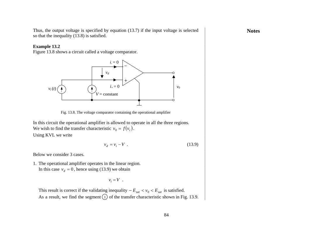
Example 13.2 Figure 13.8 shows a circuit called a voltage comparator.
vi (t)V = constant
i+ = 0
i- = 0
v0
vd
Fig. 13.8. The voltage comparator containing the operational amplifier
In this circuit the operational amplifier is allowed to operate in all the three regions. We wish to find the transfer characteristic ( )ivfv =0 . Using KVL we write
Vvv id −= . (13.9) Below we consider 3 cases. 1. The operational amplifier operates in the linear region.
0In this case =dv , hence using (13.9) we obtain
Vvi = .
This result is correct if the validating inequality satsat EvE <<− 0 is satisfied. As a result, we find the segment of the transfer characteristic shown in Fig. 13.9.
Notes
84
2. The operational amplifier operates in the +saturation region. 0>Thus, , and equation (13.9) gives dv satEv =0
2
3
. Vvi >
As a result, we obtain the segment of the transfer characteristic shown in Fig. 13.9.
3. The operational amplifier operates in the –saturation region. Similarly, as in case 2, we write the relations:
0<dv , satEv −=0 , Vvi < ,
which lead to segment of the characteristic (see Fig. 13.9).
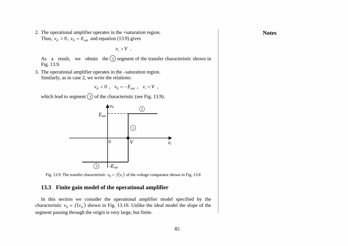
1
2
3
V 0 vi
v0
Esat
-Esat
Fig. 13.9. The transfer characteristic ( )ivfv =0 of the voltage comparator shown in Fig. 13.8
13.3 Finite gain model of the operational amplifier
In this section we consider the operational amplifier model specified by the characteristic ( )dvfv =0 shown in Fig. 13.10. Unlike the ideal model the slope of the segment passing through the origin is very large, but finite.
Notes
85

A > 100000
Slope A
0 ε
-ε
vd
v0 = f (vd)
Esat
-Esat
Fig. 13.10. The characteristic ( )dvfv =0 of nonideal model of the operational amplifier
In the linear region the model is described by the equation
dAvv =0
and the validating inequality
εε <<− dv . Hence, it follows the equivalent circuit shown in Fig. 13.11.
0=+i
0=−i
0v( )dvfv =0
dv
Fig. 13.11. The equivalent circuit of the operational amplifier operating in the linear region
Notes
86

In the +saturation region the mathematical representation of the model is
satEv =0 ,
ε>dv , whereas in the –saturation region the model is described by
satEv −=0 ,
ε−<dv , The corresponding equivalent circuits are shown in Figs 13.12 and 13.13.
0=+i
0=−i
0vsatEdv ε>dv
Fig. 13.12. The equivalent circuit of the operational amplifier operating in the +saturation region
0=+i
0=−i
0vsatEdv ε−<dv
Fig. 13.12. The equivalent circuit of the operational amplifier operating in the -saturation region
Notes
87
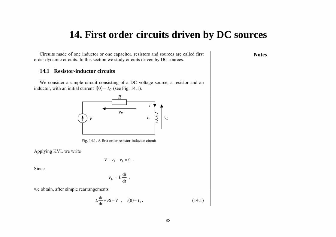
14. First order circuits driven by DC sources
Circuits made of one inductor or one capacitor, resistors and sources are called first order dynamic circuits. In this section we study circuits driven by DC sources.
14.1 Resistor-inductor circuits
We consider a simple circuit consisting of a DC voltage source, a resistor and an
inductor, with an initial current ( ) 00 Ii = (see Fig. 14.1).
V
i
R
L vL
vR
Fig. 14.1. A first order resistor-inductor circuit Applying KVL we write
0=−− LR vvV .
Since
tiLvL d
d= ,
we obtain, after simple rearrangements
VRitiL =+
dd , ( ) 00 Ii = . (14.1)
Notes
88

Equation (14.1) can be presented in the form
VL
iti 11
dd
=+τ
, (14.2)
where
RL
=τ (14.3)
is called a time constant. We rewrite equation (14.2) in the form
ττ
τ
τ
iRVi
LV
iVLt
i −=
−=−=
11dd
and separate the variables and i t
τt
RVi
i dd−=
− . (14.4)
Next, we integrate equation (14.4)
∫∫ −=−
t
RVi
i d1dτ
,
finding
KtRVi +−=−
τln ,
where the constant K may be written as AK ln= , where A is another constant.
Notes
89

Hence, we have
τt
ARVi
−=−
ln ,
or
τt
ARVi
−+= e . (14.5)
To determine A we write equation (14.5) at 0=t and set ( ) 00 Ii =
ARVI +=0 . (14.6)
Substituting A , given by (14.6) into equation (14.5) yields
( ) τt
RVI
RVti
−⎟⎠⎞
⎜⎝⎛ −+= e0 . (14.7)
When 0=t , we have , which is the correct initial conditions. When , the
second term on the right side of equation (14.7) vanishes, hence, it holds
( ) 00 Ii = ∞→t
( )RVi =∞ .
Thus, we have
( ) ( ) ( ) ( )( ) τt
iiiti−
∞−+∞= e0 , (14.8)
where ( )0i is the initial value of ( )ti , whereas ( )∞i is the steady-state value of ( )ti . Since the steady-state current is constant, the voltage across the inductor
tiLvL d
d=
equals zero.
Notes
90
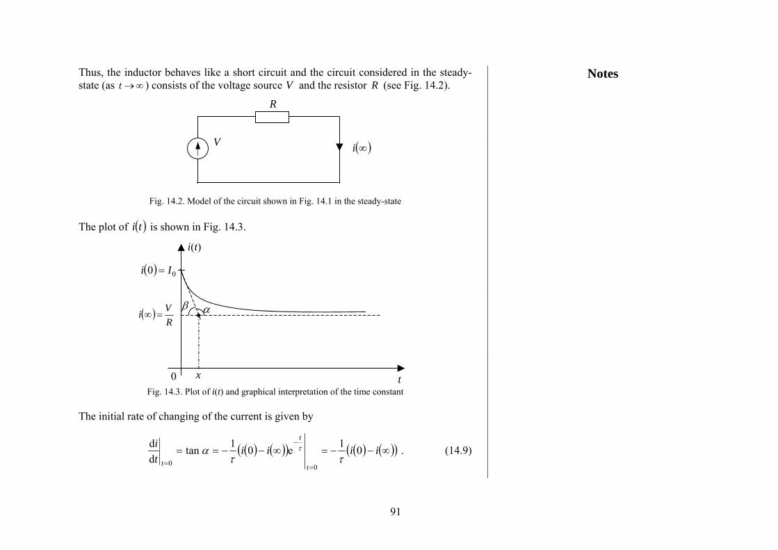
Thus, the inductor behaves like a short circuit and the circuit considered in the steady-state (as ∞→t ) consists of the voltage source V and the resistor R (see Fig. 14.2).
V
R
( )∞i
Fig. 14.2. Model of the circuit shown in Fig. 14.1 in the steady-state
The plot of ( )ti is shown in Fig. 14.3.
( ) 00 Ii =
β α
x
( )RVi =∞
0 t
i(t)
Fig. 14.3. Plot of i(t) and graphical interpretation of the time constant
The initial rate of changing of the current is given by
( ) ( )( ) ( ) ( )( )∞−−=∞−−===
−
=
iiiiti
t
t
t01e01tan
dd
00 ττα τ . (14.9)
Notes
91

On the other hand
( ) ( )( )x
iiti
t
∞−−=−=
=
0tandd
0β . (14.10)
Equalizing (14.9) and (14.10) we find
τ=x .
Thus, to find graphically the time constant, it is necessary to draw the tangent of the current at 0=t and determine its intercept with the horizontal line passing through the point ( )( )∞i,0 .
In a very special case, when 0=V , ( ) 0=∞i and equation (14.8) becomes
( ) τt
Iti−
= e0 . (14.11)
The plot of ( )ti is shown in Fig. 14.4 and the time constant x=τ .
x
0.368 I0
0
I0
t
i(t)
Fig. 14.4. Plot of i(t) in the circuit with V=0
At τ=t , ( ) 01
00 3680ee I.IIi === −−ττ
τ . Thus, in one time constant the current has declined to 0.368 of its initial value (see Fig. 14.4).
Notes
92

At τ5=t , ( ) 05
0 00670e5 I.Ii == −τ and the current is a negligible fraction of its initial value. Therefore, we usually assume that after 5 time constants the current is in the steady state. Example 14.1 The switch in the circuit shown in Fig. 14.5 is open until the steady state prevails and then it is closed. Assuming that the closing occurs at 0=t , we find the current ( ) . tiL
R1 V
iL R2
L vL
t = 0
Fig. 14.5. A first order circuit driven by a DC voltage source
When the switch is open, the circuit is in the steady state. The current is constant, hence,
the voltage across the inductor, given by tiLvL d
d= , is equal to zero. In such a case, the
inductor can be replaced by a short circuit and the circuit consists of the DC voltage source and resistors , connected in series. At the left hand side of 01R 2R =t , labeled
, the switch is open and −0
( )21
0RR
ViL +=− .
At the switch is closed. However, the current 0=t ( )ti L flowing through the inductor remains unchanged at this moment, due to the continuity property
( ) ( )21
00RR
Vii LL +== − . (14.12)
Notes
93
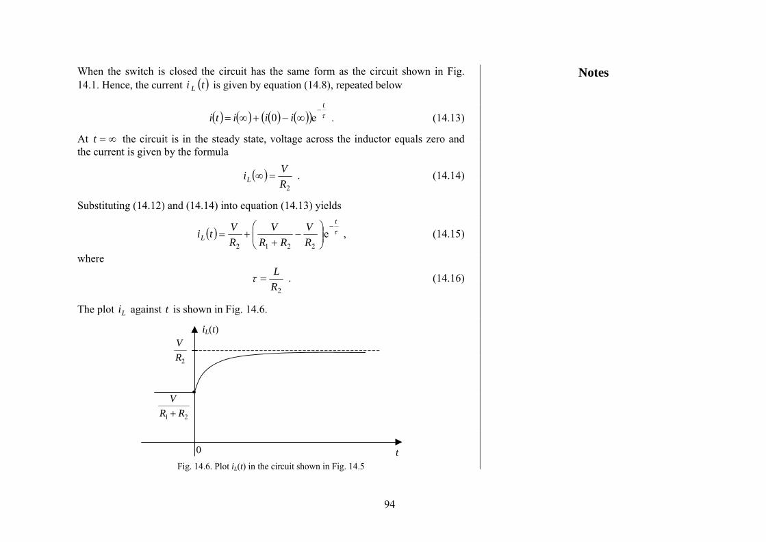
When the switch is closed the circuit has the same form as the circuit shown in Fig. 14.1. Hence, the current ( ) is given by equation (14.8), repeated below ti L
( ) ( ) ( ) ( )( ) τt
iiiti−
∞−+∞= e0 . (14.13)
At the circuit is in the steady state, voltage across the inductor equals zero and the current is given by the formula
∞=t
( )2R
ViL =∞ . (14.14)
Substituting (14.12) and (14.14) into equation (14.13) yields
( ) τt
L RV
RRV
RVti
−
⎟⎟⎠
⎞⎜⎜⎝
⎛−
++= e
2212 , (14.15)
where
2R
L=τ . (14.16)
The plot against is shown in Fig. 14.6. Li t
21 RRV+
2RV
0 t
iL(t)
Fig. 14.6. Plot iL(t) in the circuit shown in Fig. 14.5
Notes
94

Now we consider a general class of first order circuits consisting of DC sources, resistors, and one inductor. We extract the inductor from the circuit, obtaining the circuit shown in Fig. 14.7.
L vL
iL
Fig. 14.7. Circuit with the extracted inductor
Then, we apply the Thevenin theorem to reduce the circuit to the form shown in Fig. 14.8.
Req
V0C
L vL
iL
Fig. 14.8. The Thevenin circuit of the resistive one-port shown in Fig. 14.7
In this circuit the current is given by equation (14.8) repeated below
Notes
95

( ) ( ) ( ) ( )( ) τt
LLLL iiiti−
∞−+∞= e0 ,
where
( )eq
CL R
Vi 0=∞ and
eqRL
=τ .
14.2 Resistor-capacitor circuits
Another first order dynamic circuit is an RC circuit consisting of one capacitor,
resistors, and sources. In this section we study circuits driven by DC sources. Let us consider a simple RC circuit, driven by a DC voltage source, as shown in Fig.
14.9.
V iC
R
C vC
vR
Fig. 14.9. A first order RC circuit
To describe the circuit we write KVL equation
Vvv CR =+ ,
where CR Riv = and
t
vCi C
C dd
= .
Notes
96

Hence, we have
Vvt
vRC C
C =+d
d , (14.17)
We divide both sides of equation (14.17) by RC
VRC
vRCt
vC
C 11d
d=+
and define the time constant
RC=τ . (14.18)
As a result, we obtain the equation
Vvt
vC
C
ττ11
dd
=+ , (14.19)
with the initial condition
( ) 00 VvC = .
Thus, the circuit shown in Fig. 14.9 is described by equation (14.19). From a mathematical point of view this equation is similar to equation (14.2), therefore, its solution is as follows
( ) ( ) ( ) ( )( ) τt
CCCC vvvtv−
∞−+∞= e0 , (14.20)
where ( )∞Cv is the steady state solution, at ∞=t . Thus, the voltage at the steady state is constant, its derivative equals zero. This means that no current flows through the capacitor in the steady state. Consequently, the capacitor can be removed and the circuit, in the steady state, becomes as shown in Fig. 14.10.
Cv
Using KVL in the circuit depicted in Fig. 14.2 we find
( ) VvC =∞ .
Notes
97

( )∞Cv V R
( ) 0=∞Ci
Fig. 14.10. The circuit of Fig. 14.9 at the steady state
Figures 14.11 and 14.12 show the plot ( )tvC in two cases: when ( )0CvV > and when ( ). The graphical interpretation of the time constant is also shown in these
figures. 0CvV <
τ
( ) VvC =∞
0
vC(0)
t
vC(t)
Fig. 14.11. Plot ( )tvC , ( )0CvV >
τ
( ) VvC =∞
0
vC (0)
t
vC(t)
Fig. 14.12. Plot ( )tvC , ( )0CvV <
Notes
98

The current ( )tiC is given by
( ) ( )( ) ( ) ( ) ττ
τ
tCC
t
CCC
C Rvv
vvCt
vCi
−− −∞=⎟
⎠⎞
⎜⎝⎛∞−== e
0e1-0
dd .
Its plot is shown in Fig. 14.13.
0
iC(0)
t
iC(t)
Fig. 14.13. Plot of current iC against time
Alternatively, the current can be found as follows. Fist we compute the voltage
(see Fig. 14.9) using KVL Rv
( ) ( ) ( )( ) ( )( ) ττt
C
t
CCR vVVvVVtvVtv−−
−=⎟⎟
⎠
⎞
⎜⎜
⎝
⎛−+−=−= e0e0 .
Next, we apply Ohm’s law
( ) τt
CRC R
vVRvi
−−== e0 .
Now we consider a circuit consisting of DC sources, resistors, and one capacitor. We extract the capacitor from the circuit, obtaining the circuit shown in Fig. 14.14.
Notes
99

CvC
iC
Fig. 14.14. Circuit with the extracted capacitor
Next, we apply Thevenin’s theorem to reduce the circuit to the form shown in Fig. 14.15.
Req
V0C
C vC
iC
Fig. 14.15. The Thevenin circuit of the resistive one-port shown in Fig. 14.14
In this circuit the voltage is given by equation (14.20) repeated below ( )tvC
( ) ( ) ( ) ( )( ) τt
CCCC vvvtv−
∞−+∞= e0 (14.21)
where ( ) CC Vv 0=∞ and CReq=τ .
Notes
100

Example 14.2 In the circuit shown in Fig. 14.16 the switch has been open for a long time prior to 0 when it is closed. Find the voltage =t ( )tv for 0≥t . C
R3 = 5 Ω
R1 = 10 Ω
VS = 12 V iC (t)
R2 = 10 ΩC = 1μF
t = 0 vC (t)
Fig. 14.16. An example first order dynamic circuit
Since at , the circuit is in the steady state, no current flows through the
capacitor and the circuit becomes as shown in Fig. 14.17. −= 0t
R3
R1
VS ( ) 00 =−
Ci
( )−0Cv
Fig. 14.17. Model of the circuit shown in Fig. 14.16 at −= 0t
In the circuit of Fig. 14.17 it holds
( ) SC Vv =−0 .
Notes
101

Since the capacitor satisfies the continuity property
( ) ( ) SCC Vvv == −00 .
When the switch is closed the circuit has the form shown in Fig. 14.18.
R3
R1
VS R2 C vC (t)
Fig. 14.18 The circuit of Fig. 14.16 when the switch is closed
It consists of a resistive one-port terminated by the capacitor . Using Thevenin’s theorem we obtain the equivalent circuit shown in Fig. 14.19, where
C
Ω1021
213 =
++=
RRRRRReq ,
V6221
0 =+
= RRR
VV S
C .
Req
V0C iC
C vC (t)
Fig. 14.19. Circuit equivalent to the circuit of Fig. 14.18
Notes
102

In the circuit shown in Fig. 14.19 the voltage ( )tvC is given by equation (14.21) repeated below
( ) ( ) ( ) ( )( ) τt
CCCC vvvtv−
∞−+∞= e0 , where S . 10 5−== CReqτ
In the steady state the voltage is constant, hence, Cv 0d
d==
tv
Ci CC and
( ) V60 ==∞ CC Vv . Having ( ) V6=∞Cv , ( ) V120 == SC Vv , , we obtain S10 5−=τ
( ) ⎟⎟
⎠
⎞
⎜⎜
⎝
⎛+= −
− 510e66t
C tv .
The plot of ( )tvC is shown in Fig. 14.20.
t
vC (t)
12
6
0
Fig. 14.20. Plot of ( )tvC in the circuit shown in Fig. 14.17
Notes
103

15. Sinusoidal steady-state analysis
15.1 Preliminary discussion
The proceeding discussion was focused on the analysis of circuits driven by constant sources. However, many signals encountered in practice are time-varying. In power systems the sinusoidal signal is the most popular. In this section we concentrate on the analysis of linear circuits driven by sinusoidal sources.
Let us consider a sinusoidal signal
( ) tAtf ωcos= , (15.1)
where A is called an amplitude and ω is called an angular frequency measured in radians/second (abbreviated to sr ). The signal (15.1) repeats itself after every T seconds, where T is called a period. The product of ω and t is an angle in radians. The angle corresponding to one period is π2 radians. Therefore, we may write
Tωπ =2 or
ωπ2
=T . (15.2)
The number of periods completed each second is known as the frequency of the signal. Thus, the frequency is given by
f
T
f 1= .
The unit of frequency is hertz (abbreviated to Hz). Using equation (15.2) we have
fT
ππω 22== .
Notes
104
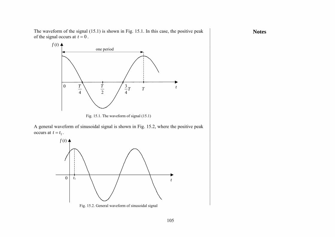
The waveform of the signal (15.1) is shown in Fig. 15.1. In this case, the positive peak of the signal occurs at 0=t .
one period
4T t T
43 0
2T
f (t)
T
Fig. 15.1. The waveform of signal (15.1)
A general waveform of sinusoidal signal is shown in Fig. 15.2, where the positive peak occurs at 1tt = .
t1 t 0
f (t)
Fig. 15.2. General waveform of sinusoidal signal
Notes
105

This signal can be expressed as follows
( ) ( ) ( ) ( )φωωωω +=−=−= tAttAttAtf coscoscos 11 (15.3)
where
112 tT
t πωφ −=−= (15.4)
is called an initial phase or simply a phase. Example 15.1 Let us consider a sinusoidal voltage, shown in Fig. 15.3.
5
11.51.5 t (ms) 0
v (t) (V)
Fig. 15.3. An example of a sinusoidal voltage
The quantities characterising this signal are as follows:
V5=A , ms10=T ,
Notes
106

Hz10010101
3 =⋅
=−
f ,
sr62810022 =⋅== ππω f ,
radians30511022
1 πππφ ..tT
−=−=−= .
In practice however, we use degrees for the phase, because we have a physical feel for angles measured in degrees.
°→180Since π , then °−=°⋅−→− 541803030 .. π . Using the obtained results we may write
( ) ( )°−= 54628cos5 ttv .
Note that for any integer it holds n
( ) ( )ntAtA πφωφω 2coscos ++=+ .
Hence, there are infinitely many phases specified by nπφ 2+ . To determine the phase uniquely we chose the positive peak of the sinusoidal signal closed to the origin, as in Example 15.1.
Consider two sinusoidal signals at the same frequency
( )atA)t(a φω += cos and ( )btB)t(b φω += cos .
If ba φφ ≠ , then the phase difference between them is defined as
ba φφ − . If ba φφ > then ( )ta is said to lead ( )tb by ( )ba φφ − . If ba φφ < , then ( )ta is said to lag behind ( )tb by ( )ab φφ − .
Notes
107

Example 15.2 We calculate the phase difference between the current
( ) ( )A10700cos20 °+= tti
and the voltage
( ) ( )V50700sin100 °+= ttv .
We cannot do it directly, because the current and the voltage have different forms, one is cosine whereas the other is sine. Therefore, we first convert ( )tv to a cosine expression using the trigonometric identity
( )°−= 90cossin αα .
As a result, we obtain
( ) ( ) ( )V40700cos1009050700cos100 °−=°−°+= tttv .
Hence, the phase difference between ( )tv and ( )ti is
°−=°−°−=− 501040iv φφ .
This means that ( )tv lags behind ( )ti by . °50
15.2 Phasor concept We will study linear circuits, driven by sinusoidal sources at the same frequency, in
the steady-state. In such a case, all branch currents and voltages have sinusoidal waveforms. The sinusoidal steady-state analysis is called AC analysis. An efficient approach to the AC analysis uses the concept of phasors.
Let us consider a sinusoidal signal
( )φω +tAmcos . (15.5)
To his signal we associate a complex number A called a phasor, according to the rule
Notes
108

. (15.6) φjemAA =
Thus, for the given sinusoid the phasor is specified uniquely. Conversely, knowing the frequency ω , the phasor A specifies uniquely the sinusoid by the formula
( ) ( )( ) ( )φωφωω +== + tAAA mt
mt
m coseReeRe jj . (15.7)
To illustrate graphically the relation between sinusoidal function (15.5) and associated phasor (15.6) we consider the expression
( )φωω += tm
t AA jj ee . (15.8)
In the complex plane this expression describes a vector rotating counter-clockwise at the angular velocity of ω , as shown in Fig. 15.4.
φ
( )tA ωjeIm
( )tA ωjeRe
φjemAA =
1je tA ω
2je tA ω
φcosmA0
( )φω +1cos tAm
( )φω +2cos tAm
Fig. 15.4. Rotating phasor
At , we have . This is a complex number that we may plot as a vector. For any expression (15.8) represents a vector having the same length
0=t φω jj ee mt AAA ==
0>t
mt AAA ==ωje and the phase equal to φω +t . Thus, the phase of the vector
increases, which means that it rotates counter-clockwise.
Notes
109

Next we project orthogonally the tip of the vector on the horizontal axis and label it ( ) . Hence, according to Euler’s formula, we obtain tx
( ) ( ) ( )φωφωφω +++=+ tAtAA mmt
m sinjcose j , ( ) ( )φω += tAtx mcos .
Thus, sinusoidal function (15.5) equals the orthogonal projection of the phasor rotating counter-clockwise at the angular velocity of ω .
15.3 Phasor formulation of circuit equations
Let us consider a linear circuit driven by sinusoidal sources, all at the same frequency ω . In the steady-state all branch voltages and currents in this circuit are sinusoidal at the frequency ω . Figure (15.5) shows an arbitrary node of the circuit.
i1(t)
i3(t) i4(t)
i2(t)
Fig. 15.5. A node of the circuit
The sinusoidal currents flowing through the branches meeting at this node are labeled as follows
( ) ( )11
cos1 im tIti φω += , ( ) ( )22
cos2 im tIti φω += ,
( ) ( )33
cos3 im tIti φω += , ( ) ( )44
cos4 im tIti φω += .
Notes
110
KVL applied at the node gives
( ) ( ) ( ) ( ) 04321 =+−− titititi . (15.9)
Now, we write this equation in terms of the phasors
04321 =+−− IIII . (15.10)
Below it is proved that equation (15.10) implies equation (15.9). tωjWe multiply both sides of equation (15.10) by e
(15.11) 0eeee j4
j3
j2
j1 =+−− tttt IIII ωωωω
and create the phasors of the sinusoidal currents ( ) ( )ti,,ti 41 … :
11
j1 e i
mII φ= , , , . 22
j2 e i
mII φ= 33
j3 e i
mII φ= 4
4
j4 e i
mII φ=
Hence, it holds ( ) ( ) ( ) ( ) 0eeee 4
43
32
21
1
jjjj =+−− ++++ iiii tm
tm
tm
tm IIII φωφωφωφω . (15.12)
Next, we apply Euler’s formula to each term of equation (15.12), finding after simple rearrangements
ααα jsincose j +=
( ) ( ) ( ) ( )( ) ( ) ( ) ( )[ ] .tItItItI
tItItItI
imimimim
imimimim
0sinsinsinsinj
coscoscoscos
4433211
44332211
2 =+++−+−++
++++−+−+
φωφωφωφω
φωφωφωφω (15.13)
Equation (15.13) holds if both the real and the imaginary part is equal to zero. Hence, we may write
( ) ( ) ( ) ( ) 0coscoscoscos44332211=+++−+−+ imimimim tItItItI φωφωφωφω .(15.14)
We recognize the terms of equation (15.14) as the sinusoidal currents ( ) ( )ti,,ti 41 … and rewrite this equation in the form
( ) ( ) ( ) ( ) 04321 =+−− titititi ,
Notes
111

being KCL equation (15.9). In this way, we have proved that equation (15.10) implies equation (15.9). Thus, in the sinusoidal steady-state KCL equations can be written down directly in terms of phasors, replacing any sinusoid by its phasor. Similarly, we prove that KVL equations can be written down directly in terms of phasors. Branch equations Linear resistor Let us consider a linear resistor as shown in Fig. 15.6.
R i(t)
v(t) Fig. 15.6. A linear resistor
The resistor is described by Ohm’s law
( ) ( )tRitv = , (15.15)
where we assume that and ( )ti ( )tv are sinusoids at the same frequency ω : ( ) ( )vm tVtv φω += cos , ( ) ( )im tIti φω += cos .
We form the corresponding phasors , and formulate the equation vmVV φje= i
mII φje=
RIV = . (15.16)
Below it is proved that equation (15.16) implies equation (15.15). tωjeLet us multiply both sides of equation (15.16) by
(15.17) tt RIV ωω jj ee =
and present the phasor and V I in the polar form
. tm
tm
iv RIV ωφωφ jjjj eeee =
Notes
112
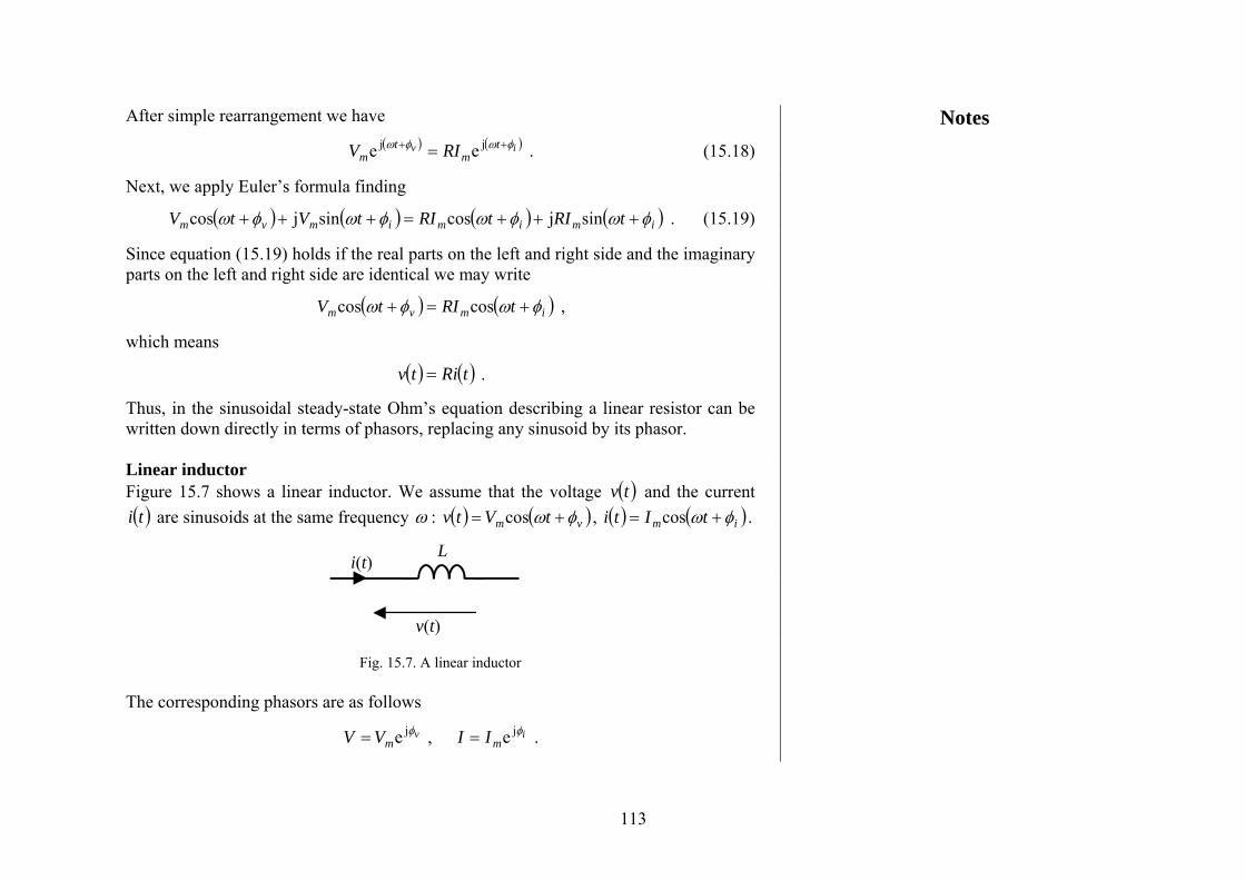
After simple rearrangement we have
( ) ( )iv tm
tm RIV φωφω ++ = jj ee . (15.18)
Next, we apply Euler’s formula finding
( ) ( ) ( ) ( )imimimvm tRItRItVtV φωφωφωφω +++=+++ sinjcossinjcos . (15.19)
Since equation (15.19) holds if the real parts on the left and right side and the imaginary parts on the left and right side are identical we may write
( ) ( )imvm tRItV φωφω +=+ coscos ,
which means
( ) ( )tRitv = .
Thus, in the sinusoidal steady-state Ohm’s equation describing a linear resistor can be written down directly in terms of phasors, replacing any sinusoid by its phasor. Linear inductor Figure 15.7 shows a linear inductor. We assume that the voltage ( )tv and the current ( ) are sinusoids at the same frequency ti ω : ( ) ( )vm tVtv φω += cos , ( ) ( )im tIti φω += cos .
L i(t)
v(t)
Fig. 15.7. A linear inductor The corresponding phasors are as follows
vmVV φje= , . i
mII φje=
Notes
113

In the time domain an inductor is described by the equation
( ) ( )ttiLtv
dd
= . (15.20)
We write the corresponding equation in terms of phasors
LIV ωj= (15.21)
and prove that equation (15.21) implies equation (15.20). For this purpose we multiply both sides of equation (15.21) by tωje
. (15.22) tt LIV ωω ω jj eje =
Since 2j
ejπ
= we rewrite equation (15.22) in the form
( ) ⎟⎠⎞
⎜⎝⎛ ++
+ = 2j
j eeπφω
φω ωi
vt
mt
m LIV . (15.23)
Next, we apply Euler’s formula to the exponential functions
( )
( )
.tLItLI
tVtV
imim
vmvm
⎟⎠⎞
⎜⎝⎛ +++⎟
⎠⎞
⎜⎝⎛ ++=
=+++
2sinj
2cos
sinjcosπφωωπφωω
φωφω (15.24)
Equation (15.24) is satisfied if the real parts on the left and right side are identical. Hence, we may write
( )
( ) ( )( ) ,tIt
LtLI
tLItV
imim
imvm
φωφωω
πφωωφω
+=+−=
=⎟⎠⎞
⎜⎝⎛ ++=+
cosddsin
2coscos
or
( ) ( )ttiLtv
dd
= .
Notes
114

Thus, equation (15.21) implies equation (15.20). Linear capacitor
C i(t)
v(t) Fig.15.8. A linear capacitor
In the time domain a linear capacitor is described by the equation
( ) ( )ttvCti
dd
= . (15.25)
The corresponding equation in terms of phasors is
CVI ωj= . (15.26)
It can be rewritten in the form
IC
IC
Vωω
jj
1−== . (15.27)
The crucial point is that, in terms of phasors, branch equations (15.15), (15.21) and (15.27) become algebraic equations with complex coefficients.
15.4 Impedance and admittance
Consider the circuit shown in Fig. 15.9, where the one-port consists of linear resistors, inductors and capacitors. Let the port voltage and the port current be sinusoidal functions of time. Their phasors are indicated in this figure.
We define the impedance of the one-port as the ratio of the voltage phasor and the current phasor
VI , that is
IVZ = . (15.28)
Notes
115

V
I
Fig. 15.9. A linear one-port
Setting vVV φje= and iII φje= we have
φjeZZ = (15.29)
where
IV
Z = and iv φφφ −= .
The impedance Z given by the expression (15.28) can be transformed into rectangular representation using Euler’s formula. As a result we obtain
φφ sinjcos ZZZ += . (15.30)
Denoting
RZZ == φcos and XZZ == φsin
we have
XRZ j+= , (15.31)
Notes
116

where R is called resistance or the resistive part of the impedance and X is called reactance or the reactive part of the impedance. Both R and X are measured in ohms. On the basis of (15.31) we find the magnitude of the impedance
22 XRZ += (15.32)
and the phase angle
RX1tan−=φ . (15.33)
The relationships (15.32) and (15.33) enable us to create a triangle in the complex plane, shown in Fig. 15.10. It is called an impedance triangle.
Z
φ
0
Im (Z)
Re (Z)
X
R
Fig. 15.10. The impedance triangle
Let us consider the series connection of two circuit elements specified by their
impedances and (see Fig. 15.11). 1Z 2Z
V
Z1 I
V1
Z2
V2
Fig. 15.11. Series connection of two elements
Notes
117

We write KVL equation
21 VVV +=
and find
2121 ZZ
IVV
IVZ +=
+== .
Thus, the impedance of two elements connected in series is the sum of their impedances.
The reciprocal of the impedance Z , labeled , is called the admittance Y
Z
Y 1= . (15.34)
The units of admittance are siemens, abbreviated to S. Substituting (15.29) into (15.34) gives
φφ
jj e1
e11 −===
ZZZY . (15.35)
Thus, the magnitude of the admittance is equal to the inverse of the magnitude of the impedance
Z
Y 1= , (15.36)
whereas the phase of the admittance equals the phase of the impedance with the opposite sign ( )φ− . Plugging (15.31) into (15.34) yields
222222 jjj
1XR
XXR
RXRXR
XRY
+−
+=
+−
=+
= .
Notes
118
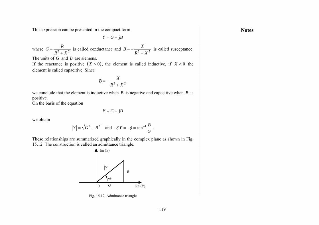
This expression can be presented in the compact form
BGY j+=
where 22 XRRG+
= is called conductance and 22 XRXB+
−= is called susceptance.
The units of and G B are siemens. (If the reactance is positive , the element is called inductive, if the
element is called capacitive. Since )0>X 0<X
22 XRXB+
−=
we conclude that the element is inductive when B is negative and capacitive when B is positive. On the basis of the equation
BGY j+=
we obtain 22 BGY += and
GBY 1tan −=−=∠ φ .
These relationships are summarized graphically in the complex plane as shown in Fig. 15.12. The construction is called an admittance triangle.
Y
-φ
0
Im (Y)
Re (Y)
B
G
Fig. 15.12. Admittance triangle
Notes
119
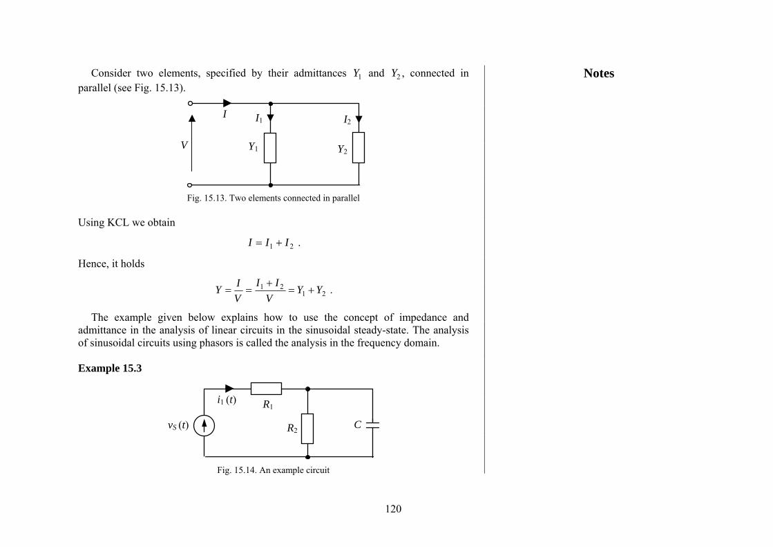
Consider two elements, specified by their admittances and , connected in parallel (see Fig. 15.13).
1Y 2Y
I2
Y2 V
I1 I
Y1
Fig. 15.13. Two elements connected in parallel
Using KCL we obtain
21 III += .
Hence, it holds
2121 YY
VII
VIY +=
+== .
The example given below explains how to use the concept of impedance and admittance in the analysis of linear circuits in the sinusoidal steady-state. The analysis of sinusoidal circuits using phasors is called the analysis in the frequency domain.
Example 15.3
C R2 vS (t)
i1 (t) R1
Fig. 15.14. An example circuit
Notes
120

Consider the circuit shown in Fig. 15.14, driven by the sinusoidal voltage source
( ) ( )V451000cos1414 °+= t.tvS .
We wish to find the steady state current ( )ti1 using the phasor concept. The phasor of ( )tvS is
. Ve1414 45j °= .VS
Figure 15.15 shows the circuit in a phasor format.
ZC Z2=R2 VS
I1 Z1=R1
Fig. 15.15. The circuit of Fig. 15.14 in phasor format
We compute the impedance faced by the voltage source. Since the elements specified by impedances and are connected in parallel we find the admittance 2Z CZ
C
CC ZZYYY 11
222 +=+= .
Hence, the impedance is CZ2
CR
CR
ZZZZ
YZ
C
C
CC
ω
ωj
j1
2
2
2
2
22
−
⎟⎠⎞
⎜⎝⎛−
=+
== .
Notes
121
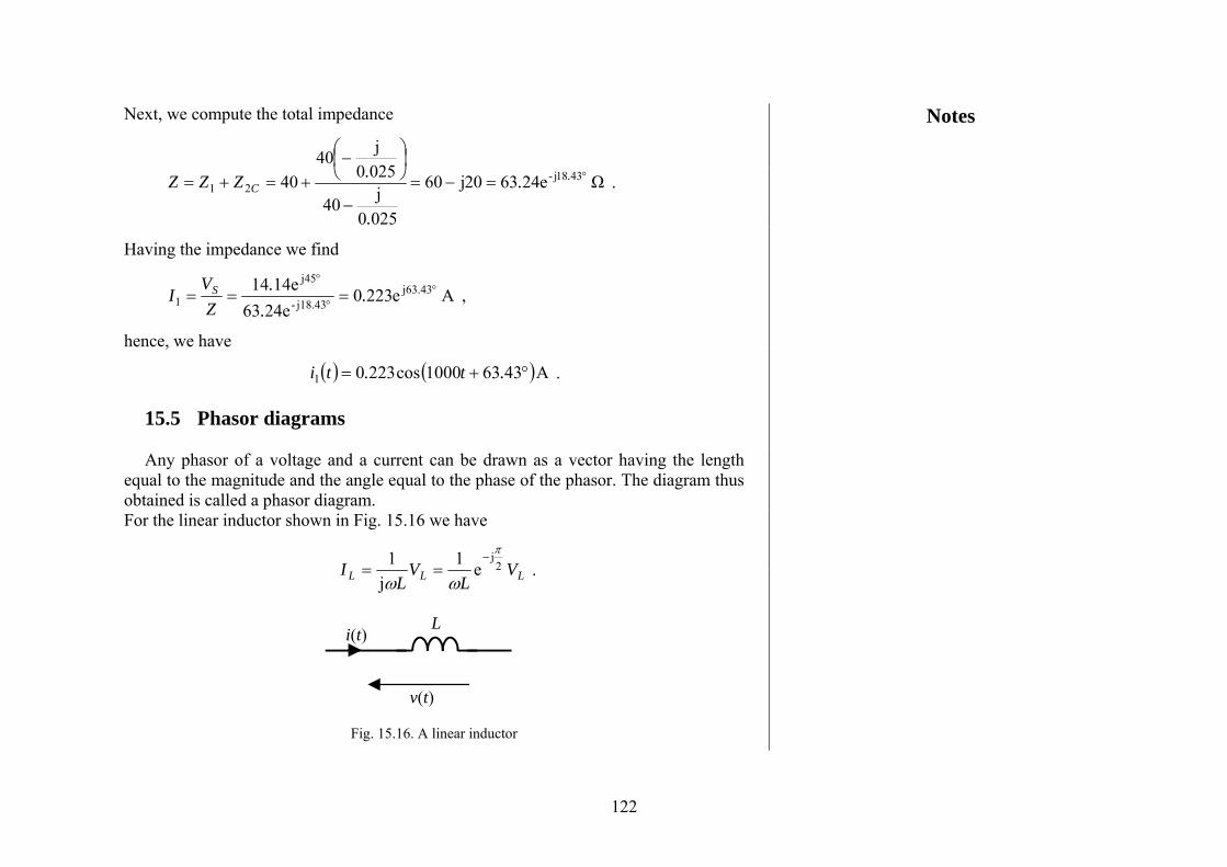
Next, we compute the total impedance
Ωe246320j60
0250j40
0250j40
40 4318j-21
°=−=−
⎟⎠⎞
⎜⎝⎛−
+=+= .C .
.
.ZZZ .
Having the impedance we find
Ae2230e2463e1414 43j63.
43j18.-
45j
1°
°
°
=== ...
ZV
I S ,
hence, we have
( ) ( )A43631000cos22301 °+= .t.ti .
15.5 Phasor diagrams
Any phasor of a voltage and a current can be drawn as a vector having the length equal to the magnitude and the angle equal to the phase of the phasor. The diagram thus obtained is called a phasor diagram. For the linear inductor shown in Fig. 15.16 we have
LLL VL
VL
I 2j
e1j1 π
ωω−
== .
L i(t)
v(t)
Fig. 15.16. A linear inductor
Notes
122

Using the voltage phasor as the horizontal reference we draw the phasor vertically downward as shown in Fig. 15.17.
LV LI
VL
2πφ −=i
IL Fig. 15.17. Phasor diagram of the inductor
We say that the inductor current lags behind the inductor voltage by 2π .
For the capacitor shown in Fig 15.18 we write
CCC IC
IC
V 2j
e1j π
ωω−
=−= .
C i(t)
v(t) Fig. 15.18. A linear capacitor
Assuming that 0=iφ we draw the phasor diagram as depicted in Fig. 15.19.
IC
2πφ −=v
VC Fig. 15.19. Phasor diagram of the capacitor
Notes
123

We say that capacitor voltages lag behind the capacitor current by 2π .
Now we draw a phasor diagram showing the current and voltages in the circuit shown in Fig. 15.20.
L1
V2 V3
C3R2
VS
I
V1
Fig. 15.20. An example circuit
Using KVL we write
321 VVVVS ++= .
We use a current phasor as the horizontal reference. Since 2j
111 ejπ
ωω ILILV == , the
voltage leads the current by 1V2π . Consequently the phasor is drawn vertically
upward (see Fig. 15.21).
1V
I
V1
Fig. 15.21. A simple phasor diagram
Notes
124
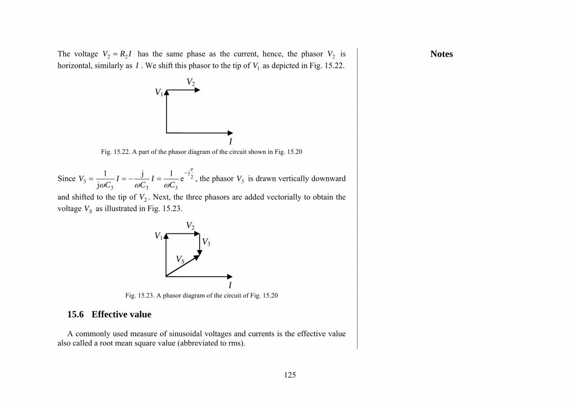
The voltage IRV 22 = has the same phase as the current, hence, the phasor is horizontal, similarly as
2VI . We shift this phasor to the tip of as depicted in Fig. 15.22. 1V
V2
I
V1
Fig. 15.22. A part of the phasor diagram of the circuit shown in Fig. 15.20
Since 2j
3333 e1j
j1 π
ωωω−
=−==C
IC
IC
V , the phasor is drawn vertically downward
and shifted to the tip of . Next, the three phasors are added vectorially to obtain the voltage as illustrated in Fig. 15.23.
3V
2V
SV
VS
V3
V2
I
V1
Fig. 15.23. A phasor diagram of the circuit of Fig. 15.20
15.6 Effective value
A commonly used measure of sinusoidal voltages and currents is the effective value
also called a root mean square value (abbreviated to rms).
Notes
125

For a sinusoidal voltage
( ) ( )vm tVtv φω += cos
it is defined as follows
( )( ) ( )( )∫∫ +===T
vm
T
rmseff ttVT
ttvT
VV0
2
0
2 dcos1d1 φω . (15.37)
To integrate, we apply the trigonometric identity
( )αα 2cos121cos2 +=
finding
( ) ( )( )
( ) .ttVTV
ttVttV
T
vmm
T
vm
T
vm
∫
∫∫
++=
=++=+
0
22
0
2
0
22
d22cos21
21
d22cos121dcos
φω
φωφω
(15.38)
In the interval T−0 there are exactly two periods of the function ( )vt φω 22cos + , consequently
. ( ) 0d22cos0
=+∫T
v tt φω
Hence, we have
( ) TVtt m
T
vm2
0
22
21d22cosV =+∫ φω
and
Notes
126

22
11 2 mmrmseff
VTV
TVV === . (15.39)
Similarly we define the effective (rms) value of the sinusoidal current
( ) ( )im tIti φω += cos
finding
2m
rmseffI
II == . (15.40)
Notes
127

16. Power in sinusoidal steady state
16.1 The instantaneous and average power
Power is a very important quantity in electrical engineering, electronics, communications, and power systems. Hence, the question arises how to define power in sinusoidal circuits.
Consider a one-port consisting of resistors, inductors and capacitors (see Fig. 16.1) with sinusoidal port voltage
( ) ( )Vcos vm tVtv φω += (16.1)
and port current
( ) ( )Acos im tIti φω += . (16.2)
V
I
Fig. 16.1. A one-port consisting of resistors, inductors and capacitors
The instantaneous power received by the one-port is given by
( ) ( ) ( ) ( ) ( )ivmm ttIVtitvtp φωφω ++== coscos . (16.3)
Notes
128

Using the trigonometric identity
( ) ( )( )yxyxyx −++= coscos21coscos
we obtain
( ) ( ) ( )ivmm
ivmm IVtIVtp φφφφω −+++= cos
22cos
2 . (16.4)
Thus, the instantaneous power is the sum of two components. The first one is a sinusoid whose frequency is twice of the voltage and current. The second component is a constant. Thus, the waveform of ( )tp is a sinusoid having the angular frequency ω2 shifted upward by the value equal to the second term.
Average power, labeled , is defined as the mean value of the instantaneous power over an interval of
avPT , where T is a period of the voltage or current
( ) ttpT
PT
av d1
0∫= . (16.5)
Substituting (16.4) into (16.5) yields
( ) ( )( )∫ −+++=T
0dcos2cos
21 tt
IVT
P ivivmm
av φφφφω .
The integral of the sinusoid ( )ivt φφω ++2cos , having the period 2T , over the interval
to 0 T is zero, because the total area under the waveform of this sinusoid is equal to zero. Hence, we have
( ) φφφφ coscos2
dcos2
1 T
0effeff
mmiv
mmav IV
IVt
IVT
P ==−= ∫ , (16.6)
Notes
129

where iv φφφ −= is called a power factor. Note that ⎥⎦⎤
⎢⎣⎡−∈
22ππφ , , 0cos ≥φ and the
average power is a real, nonnegative number.
16.2 The complex power
Another power useful in the AC analysis of circuits is the complex power defined as follows
∗= IVP21 , (16.7)
where is the phasor of the port voltage whereas V ∗I is the complex conjugate of the port current phasor. Hence, it holds
( )
( ) ( )
.effIeffVeffIeffVmImVmImV
IVIV
IVIVP
VV
IVIV
φφφφ
φφφφ
φφφφ
sinjcossin21jcos
21
sin21jcos
21
e21ee
21 jj-j
+=+=
=−+−=
=== −
(16.8)
Thus, the complex power is a complex number. The real part of this number is, according to (16.6), the average power
( )PPav Re= .
Let XRZ j+= and be the impedance and admittance of the one-port, respectively (see Fig. 16.1). Then using (16.7) we obtain
BGY j+=
( ) ( )
,RIRIRI
XRIIIZPP
effm
av
222
2
21
21
j21Re
21ReRe
===
=⎥⎦⎤
⎢⎣⎡ +=⎟
⎠⎞
⎜⎝⎛== ∗
(16.9)
Notes
130

or
( )
( ) .GVGVVGVBG
VVYVYVP
effm
av
2222
21
21j
21Re
21Re
21Re
===⎥⎦⎤
⎢⎣⎡ −=
=⎥⎦⎤
⎢⎣⎡=⎥⎦
⎤⎢⎣⎡= ∗∗∗
(16.10)
The imaginary part of the complex power, labeled , is called a reactive power, that is (see (16.8))
xP
( ) φφ sinsin21Im effeffmmx IVIVPP === . (16.11)
Similarly, as in the case of the average power, we find some alternative expression for the reactive power
( ) ( )
.XIIXIXIXIR
IXRIIZPP
effm
x
22222
2
21
21j
21Im
j21Im
21ImIm
===⎥⎦⎤
⎢⎣⎡ +=
=⎥⎦⎤
⎢⎣⎡ +=⎟
⎠⎞
⎜⎝⎛== ∗
(16.12)
or
( ) ( )
( ) .BVBVVBVBG
VVYVYVPP
effm
x
2222
21
21j
21Im
21Im
21ImIm
−=−=−=⎥⎦⎤
⎢⎣⎡ −=
=⎥⎦⎤
⎢⎣⎡=⎥⎦
⎤⎢⎣⎡== ∗∗∗
(16.13)
Thus, the complex power is the complex number whose real part is the average power and the imaginary part is the reactive power
xav PPP j+= . (16.14)
Using (16.8) we obtain
Notes
131

( )φφφφ jsincos21sin
21jcos
21
+=+= IVIVIVP .
By virtue of Euler’s formula it holds
φφφ jjj ee21e
21
effeffmm IVIVIVP === . (16.15)
Expression (16.14) and (16.15) lead to the equations
222xav PPP += (16.16)
and
av
x
PP
=φtan . (16.17)
They enable us to create the geometrical construction called a power triangle. Two variants of the power triangle are shown in Fig. 16.2.
P
φ
Px > 0
Pav
a)
P
φ
Px < 0
Pav
b)
Fig. 16.2. Two variants of the power triangle
Consider the one-port consisting of resistors, inductors and capacitors, supplied with
a sinusoidal source ( ) as shown in Fig. 16.3. tv
Notes
132

v (t)
i(t)
Fig. 16.3. One-port RLC driven by a sinusoidal voltage source
It can be proved that the complex power P of the one-port is equal to the sum of the complex powers of all elements of the one-port, i.e. kP
, (16.18) ∑=
=b
kkPP
1
where is the number of the elements. bSince
xav PPP j+= and ( ) ( ) b,,k,PPP kxkavk …1j =+= ,
equation (16.18) leads to two equations
, (16.19) ( )∑=
=b
kkavav PP
1
. (16.20) ( )∑=
=b
kkxx PP
1
Notes
133

16.3 Measurement of the average power
To measure the average power we use a wattmeter. The wattmeter is an instrument having a current coil and a voltage coil. To measure the average power of a load the coils are connected as shown in Fig. 16.4.
*
*i(t)
v(t) Load
Fig. 16.4. Measurement of the average power
The current coil is connected in series to the load, whereas the voltage coil is connected in parallel to the load. There is ∗ mark on each of the coils. They are connected as shown in Fig. 16.4. The wattmeter reading is given by
( ) ( )V,IIVVI effeff ∠=∗ cosRe21 , (16.21)
where I and are phasor of the sinusoidal voltage V ( )tv and current ( )ti , respectively. For an ideal wattmeter the impedance of the current coil tends to zero and the impedance of the voltage coil tends to infinity. As a result, the ideal wattmeter does not introduce any disturbance in the circuit. Both the current and the voltage remains the same as without the wattmeter, ( ) φ=∠ V,Icos and the wattmeter reading is the average power consumed by the load.
Notes
134

16.4 Theorem on the maximum power transfer
Consider the circuit consisting of a sinusoidal voltage source, represented by phasor and impedance , and the load represented by impedance (see Fig. 16.5). We
want to find so that the average power entering the load is maximum. SV SZ LZ
LZ
ZL Zs
I Vs
Fig. 16.5. Simple circuit terminated by load ZL
Let the impedances and be given in rectangular form SZ LZ
SSS XRZ j+= , LLL XRZ j+= .
On the basis of (16.9) the average power delivered to the load is
Lav RIP 2
21
= .
Since
LS
S
ZZV
I+
=
it follows
( ) ( ).
XXRRRV
XRXR
RVRZZ
VR
ZZV
P
LSLS
LS
LLSS
LSL
LS
SL
LS
Sav
222
22
2
22
21
jj21
21
21
+++=
=+++
=+
=+
=
Notes
135
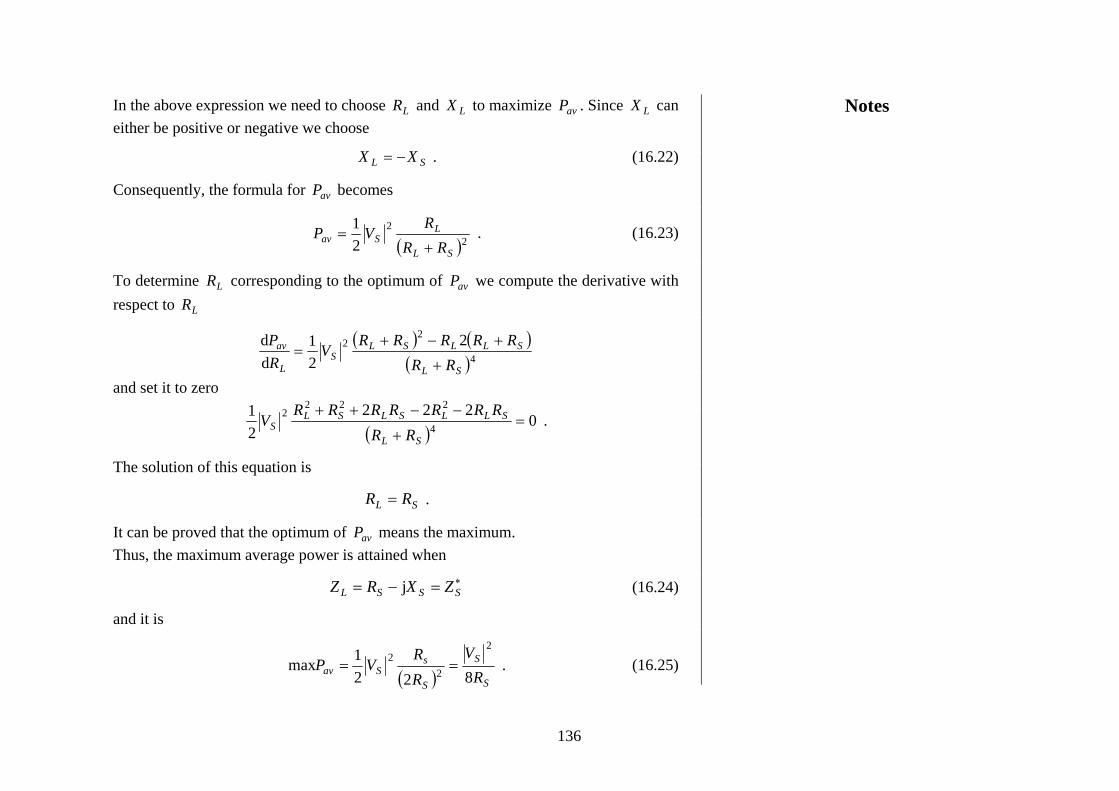
In the above expression we need to choose and to maximize . Since can either be positive or negative we choose
LR LX avP LX
SL XX −= . (16.22)
Consequently, the formula for becomes avP
( )2
2
21
SL
LSav
RRR
VP+
= . (16.23)
To determine corresponding to the optimum of we compute the derivative with respect to
LR avP
LR
( ) ( )( )4
22 2
21
dd
SL
SLLSLS
L
av
RRRRRRR
VRP
+
+−+=
and set it to zero
( )
0222
21
4
2222 =
+
−−++
SL
SLLSLSLS
RRRRRRRRR
V .
The solution of this equation is
. SL RR =
It can be proved that the optimum of means the maximum. avPThus, the maximum average power is attained when
(16.24) ∗=−= SSSL ZXRZ j
and it is
( ) S
S
S
sSav R
V
RR
VP822
1max2
22 == . (16.25)
Notes
136

17. Resonant circuits
17.1 Series resonant circuit
Let us consider the circuit shown in Fig. 17.1 consisting of an inductor, a capacitor and a resistor connected in series, driven by a sinusoidal voltage source.
L
VC VR
C
RVS
I
VL
Fig. 17.1. Series resonant circuit
Suppose that the voltage source is
( ) ( )SSS tVtvm
φω += cos ,
then the phasor associated to this voltage equals
. SmSS VV φje=
In Fig. 17.1 , , and are the phasors of the voltages across the elements whereas LV CV RVI is the phasor of the current traversing all the elements. The circuit can be considered a one-port supplied with a voltage source. The impedance of this circuit is given by
XRC
LRRZ j1 jC1j-Lj +=⎟
⎠⎞
⎜⎝⎛ −+=+=
ωω
ωω , (17.1)
Notes
137

where
( )C
LXXω
ωω 1−== . (17.2)
The reactance X of the one-port is a monotonically increasing function of ω , for ( )∞∈ ,0ω . It becomes zero at 0ωω = , i.e.
01
00 =−
CL
ωω . (17.3)
Solving equation (17.3) for 0ω yields
LC1
0 =ω . (17.4)
The frequency 0ω is called a resonant frequency and the circuit at this frequency is said to be in resonance. Since ( ) 00 =ωX , the impedance in resonance is equal to the resistance
( ) RXRZ =+= 00 j ω . (17.5)
Hence, the current in resonance is given by
R
VZV
I SS ==0
0 . (17.6)
At an arbitrary frequency ω the impedance of the one-port equals
( ) ( )ωω XRZ j+= . (17.7)
For each ω the impedance is represented by a vector in the complex plain as shown in Fig. 17.2. As ω varies in the interval ( )∞,0 the tip of this vector traces a straight line parallel to the imaginary axis. At 0ωω = the reactance of this impedance equals zero and its magnitude is the smallest.
Notes
138
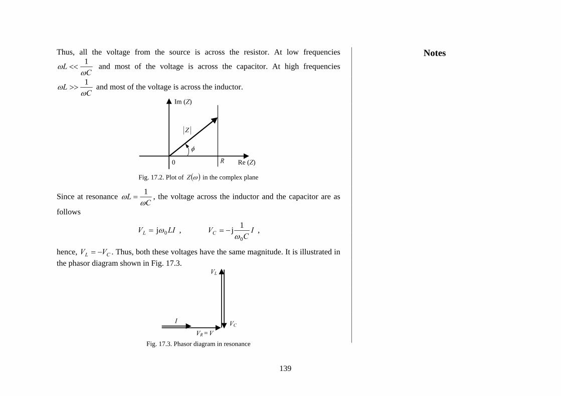
Thus, all the voltage from the source is across the resistor. At low frequencies
CL
ωω 1
<< and most of the voltage is across the capacitor. At high frequencies
CL
ωω 1
>> and most of the voltage is across the inductor.
Z
φ
0
Im (Z)
Re (Z) R
Fig. 17.2. Plot of ( )ωZ in the complex plane
Since at resonance C
Lω
ω 1= , the voltage across the inductor and the capacitor are as
follows
LIVL 0jω= , IC
VC0
1jω
−= ,
hence, CL VV −= . Thus, both these voltages have the same magnitude. It is illustrated in the phasor diagram shown in Fig. 17.3.
I
VL
VR = V VC
Fig. 17.3. Phasor diagram in resonance
Notes
139

At resonance the ratio of the magnitude of the voltage across the inductor (or capacitor) to the magnitude of the source voltage is called a quality factor and labeled Q
m
m
m
m
S
C
S
L
VV
VV
Q == at 0ωω = . (17.8)
Since
mCCmLL IC
VVLIVVmm
00
1ω
ω =====
and mSS RIVV
m== ,
then
CRR
LQ
0
0 1ω
ω== . (17.9)
Now we consider the ratio of the phasor of the voltage across the resistor to the phasor of the source voltage at any frequency ω . Since
⎟⎠⎞
⎜⎝⎛ −+
==
CLR
VRRIV S
R
ωω 1j
, (17.10)
then it holds
⎟⎠⎞
⎜⎝⎛ −+
=
CLR
RVV
S
R
ωω 1j
. (17.11)
Expression (17.11) can be rearranged as follows
⎟⎟⎠
⎞⎜⎜⎝
⎛−+
=
⎟⎟⎠
⎞⎜⎜⎝
⎛−+
=
ωω
ωωω
ωω
ω 0
0
020 j1
1
j1
1
RL
RLV
V
S
R . (17.12)
Notes
140

Using (17.9) we have
⎟⎟⎠
⎞⎜⎜⎝
⎛−+
=
ωω
ωω 0
0j1
1
QVV
S
R , (17.13)
hence, it holds
( )( ) 2
0
0
21
1
⎟⎟⎠
⎞⎜⎜⎝
⎛−+
==
ωω
ωωQ
VV
VV
Sm
Rm
S
R . (17.14)
Plots of SR VV versus ω , at different quality factors, are shown in Fig. 17.4.
ω
s
R
VV
1
0 ω0
Q=20
Q=5
Fig. 17.4. Plots of SR VV against frequency ω
Notes
141

At the resonance frequency SR VV is equal to 1, whereas at 0=ω and ∞=ω the ratio equals zero. Therefore the voltage across the resistor R is the same as the source voltage at the resonant frequency. This voltage is slightly reduced for the frequencies close to the resonance frequency and considerably reduced at low and high frequencies. Such a circuit is called a bandpass filter. The passband is defined as a range of the frequencies in the neighbourhood of the resonant frequency such that at the edges of the passband
( )( ) 2
1=
Sm
Rm
VV
. (17.15)
Substituting (17.14) into (17.15) gives
2
1
1
12
0
0
2
=
⎟⎟⎠
⎞⎜⎜⎝
⎛−+ωω
ωωQ
. (17.16)
We rearrange equations (17.16) as follows
,Q 212
0
0
2 =⎟⎟⎠
⎞⎜⎜⎝
⎛−+ωω
ωω ,Q 1
20
0
2 =⎟⎟⎠
⎞⎜⎜⎝
⎛−ωω
ωω
Q10
0±=−
ωω
ωω .
Hence, we have
Q1
2
0
0
2 =−ωω
ωω
, Q1
1
0
0
1 −=−ωω
ωω
.
or
Q
2020
22
ωωωω =− ,
Q102
021
ωωωω −=− .
Notes
142

Next we subtract both sides of the above equations
( )1202
122 ωω
ωωω +=−
Q . (17.17)
Dividing equation (17.17) by ( )12 ωω + we obtain the following expression for the passband
Q
012
ωωω =− . (17.18)
The passband is illustrated in Fig. 17.5.
the passband
ω1 ω2
ω0 ω
( )( )mS
mR
S
R
VV
VV
=
1
0
21
Fig. 17.5. The passband of a resonant circuit
Notes
143

17.2 Parallel resonant circuit
Another type of a resonant circuit is the parallel resonant circuit shown in Fig. 17.6. The circuit is driven by sinusoidal source current represented by the phasor . In Fig. 17.6 , , are phasors of the currents flowing through the circuit elements and is the phasor of the voltage across the parallel connection of these elements.
SI
CI LI RI V
IS
IC IL IR
V C L R
RG 1=
Fig. 17.6. Parallel resonant circuit
The admittance of the one-port faced by the source is
⎟⎠⎞
⎜⎝⎛ −+=++=
LCG
LCGY
ωω
ωω 1j
j1j . (17.19)
The imaginary part of (susceptance) is a function of the frequency Y ω
( )L
CBω
ωω 1−= . (17.20)
The frequency 0ωω = such that ( ) 00 =ωB is called a resonant frequency. To find this frequency, we solve the equation
01
00 =−
LC
ωω , (17.21)
finding
LC1
0 =ω . (17.22)
Notes
144

At the resonance it holds
RS IGVYVI === . (17.23)
Furthermore, since
VLL
VI L00
1jj ωω
−== (17.24)
and CVIC 0jω= , (17.25)
then CL II −= or 0=+ CL II . (17.26)
Thus, all the current from the current source goes through the resistor and the currents in the inductor and capacitor add to zero. The phasor diagram is shown in Fig. 17.7.
IC
V
IL
IR=IS
IS
IC IL
IR
C L R
I=0
Fig. 17.7. The phasor diagram Fig. 17.8. Parallel resonant circuit at 0ωω = of the resonant circuit Figure 17.8 illustrates equation (17.26).
Let us consider the ratio of the currents and at an arbitrary frequency RI SI ω and rearrange it as follows
Notes
145

.RC
RCLCG
GYVGV
II
S
R
⎟⎟⎠
⎞⎜⎜⎝
⎛−+
=
=
⎟⎟⎠
⎞⎜⎜⎝
⎛−+
=⎟⎠⎞
⎜⎝⎛ −+
==
ωω
ωωω
ωω
ωωω
0
00
20
j1
1
j1
11j
(17.27)
Since RG
=1 and 2
01 ω=
LC, then we may write
( )( )
( )( )Sm
Cm
II
VGVC
GC
R
CRC ====
0
00000 1 ω
ωωωωω . (17.28)
The ratio of the current and ( )mCI ( )mSI is called a quality factor of the parallel resonant circuit and labeled . Since at the resonance Q ( ) ( )mLmC II = , we have
( )( )
( )( ) L
RCRII
II
QmS
mL
mS
mC
00 ω
ω ==== . (17.29)
Substituting (17.29) into (17.27) yields
⎟⎟⎠
⎞⎜⎜⎝
⎛−+
=
ωω
ωω 0
0j1
1
QII
S
R . (17.30)
Hence, we obtain the equation
( )( ) 2
0
0
21
1
⎟⎟⎠
⎞⎜⎜⎝
⎛−+
==
ωω
ωωQ
II
II
mS
mR
S
R , (17.31)
illustrated in Fig. 17.8 for two values of . Q
Notes
146

ω
S
R
II
1
0 ω0
Q=20
Q=5
Fig. 17.9. Plots of SR II for different values of Q
The plots shown in Fig. 17.9 have the same shapes as in Fig. 17.5 and can be similarly interpreted. Thus, the parallel resonant circuit is a bandpass filter which passes the current through the resistor at the resonant frequency, slightly reduces the current in the neighbourhood of this frequency and considerably reduces it at a low frequency and at a high frequency. Similarly, as in the case of a series resonant circuit, the passband is defined as a range of the frequencies in the neighbourhood of the resonant frequency such that at the edges of the passband it holds
2
1=
S
R
II
. (17.32)
Hence, we obtain the following expression for the passband
Q
012
ωωω =− . (17.33)
Notes
147

18. Coupled inductors
In this section we study the circuits in which two inductors are coupled magnetically. 18.1 Basic properties Let us consider two coils, placed near each other, as shown in Fig. 18.1. If we supply
the first coil with a generator so that the current varies with time and have the second coil open, then a time-varying magnetic flux
1iφ is produced. It induces a voltage in the
second coil.
i2 = 0
v2
i1
v1
φ
Fig. 18.1. Two magnetically coupled inductors
Now we consider the case where currents and flow through the inductors. If the
core is made of nonmetallic material, the following equations relate the currents and the fluxes leakages associated with the inductors
1i 2i
Notes
148

, (18.1)
iLMi,MiiL
2212
2111
+=+=
φφ
where is the self-inductance of the inductor 1, is the self-inductance of the inductor 2, and
1L 2LM is called a mutual inductance of the inductors 1 and 2. The equality
of both mutual inductances is established in physics. By Faraday’s law we have
.
ti
Lti
Mt
v
,tiM
tiL
tv
dd
dd
dd
dd
dd
dd
22
122
211
11
+==
+==
φ
φ
(18.2)
The mutual inductance M enables us to define the coefficient of coupling as follows k
21LL
Mk = . (18.3)
It can be shown that . 1≤k
φ1
φ2φ2
φ1i1i1
i2
i2
(a) (b) Fig. 18.2. Coupled inductors with dotted terminals
Notes
149

The mutual inductance M may be positive or negative. The sign of M is specified by the reference directions of the currents and the physical arrangement of the coils. To determine the sign of M , we place a dot mark in each inductor so that, when both currents of the inductors enter them through the dotted terminals, then the fluxes due to these two currents add. This is illustrated in Fig. 18.2. Next, we determine the sign of the mutual inductance M as follows. We arbitrarily assign the reference directions of the currents and . If the reference directions of these currents are such that both currents enter the inductors through the dotted terminals or leave the inductors through the dotted terminals, then
1i 2i
M is positive. If one current enters the inductor through the dotted terminal and the other leaves the inductor through the dotted terminal, then M is negative. Thus, if M is positive, then both fluxes due to the currents and add. If 1i 2i M is negative, they subtract.
According to the rule M in Fig. 18.3a is positive, whereas in Fig. 18.3b is negative.
(a) (b)
v1
v2v2
v1i1i1
i2 i2
Fig. 18.3. Coupled inductors with positive (Fig. 18.3a) and negative (Fig. 18.3b) mutual inductance M
Dotted terminals enable us to specify the sign of M without knowing the physical arrangement of the coils. Therefore, they are introduced in circuit diagrams as shown in Fig. 18.4.
Notes
150
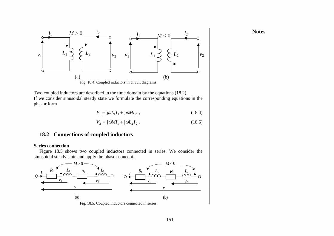
v2
M > 0
v2
M < 0
L1
i2 i1
L2 v1 L1
i2 i1
L2 v1
(a) (b) Fig. 18.4. Coupled inductors in circuit diagrams
Two coupled inductors are described in the time domain by the equations (18.2). If we consider sinusoidal steady state we formulate the corresponding equations in the phasor form
2111 jj MIILV ωω += , (18.4)
2212 jj ILMIV ωω += . (18.5)
18.2 Connections of coupled inductors Series connection
Figure 18.5 shows two coupled inductors connected in series. We consider the sinusoidal steady state and apply the phasor concept.
L2 R2
v2 v1
M > 0 L1 R1
v
I L2 R2
v2 v1
M < 0
L1 R1
v
I
(a) (b) Fig. 18.5. Coupled inductors connected in series
Notes
151

The voltage across the connection is given by V
( ) ( )
( )[ ] .IMLLRR
MIILIRMIILIRVVV
2j
jjjj
2121
221121
++++=
=+++++=+=
ω
ωωωω
Hence, we obtain the impedance of this connection, as follows
( ) eqeq LRMLLRRIVZ ωω j2j 2121 +=++++== , (18.6)
where
21 RRReq += (18.7)
and
MLLLeq 221 ++= . (18.8)
Equation (18.6) states that the series connection shown in Fig. 18.5 can be replaced by the equivalent circuit shown in Fig. 18.6.
Leq Req
V
I
Fig. 18.6. Equivalent circuit to the circuit depicted in Fig. 18.5
Note that the equivalent inductance is given by equation (18.8), where M can be either positive or negative. Figure 18.7a shows a phasor diagram for , whereas Fig. 18.8b shows a phasor diagram for 0
0>M<M .
Notes
152
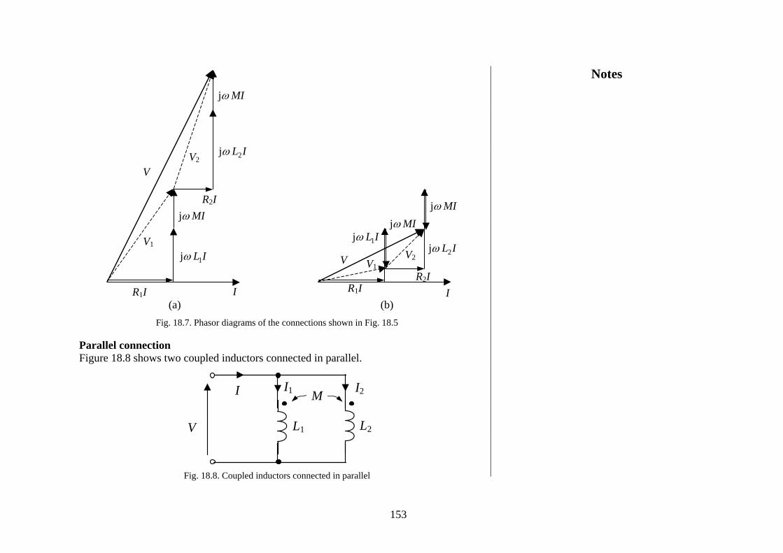
(b)
MIωj
IL2jωIL1jω
MIωj
V2V1
VR2I
R1I I
MIωj
IL2jω
IL1jω
MIωj
V2
V1
V
R2I
R1I I (a)
Fig. 18.7. Phasor diagrams of the connections shown in Fig. 18.5
Parallel connection Figure 18.8 shows two coupled inductors connected in parallel.
M
L1
I2 I1 I
L2 V
Fig. 18.8. Coupled inductors connected in parallel
Notes
153

We analyse this connection in the sinusoidal steady state using the phasor concept. As a result, we write the equations
211 jj MIILV ωω += , (18.9)
122 jj MIILV ωω += . (18.10)
Next, we solve equation (18.9) for 2I
11
2 jI
ML
MVI −=ω
(18.11)
and substitute (18.11) into (18.10)
111
22 jjj
j MIIMLL
MVLV ωωω
ω +−= .
Hence, we find the current 1I
( )
VLLM
LMV
MLL
M
ML
I21
2
2
21
2
1jj
1
−
−=
⎟⎠
⎞⎜⎝
⎛ −
−=
ωω
. (18.12)
Similarly, we obtain
( )
VLLM
LMI
212
12
j −
−=
ω . (18.13)
Taking into account (18.12) and (18.13) we have
( )
VLLM
MLLIII
212
2121
j
2
−
+−−=+=
ω . (18.14)
Notes
154

Equation (18.14) leads to
ILV eqωj= , (18.15) where
MLL
MLLLeq 221
221
−+−
= . (18.16)
Thus, the parallel connection of the coupled inductors, depicted in Fig. 18.8, is equivalent to the single inductor having the inductance specified by (18.16). To illustrate the method for the analysis of circuits containing coupled inductors, we consider the circuit shown in Fig. 18.9.
M
RLV2
R1
L1
I2 I1
V1 L2 VS
Fig. 18.9. A circuit containing coupled inductors
First we write the equations for and 1V 2V
2111 jj MIILV ωω += , (18.17)
1222 jj MIILV ωω += . (18.18)
Then, we apply KVL in the two loops
111 VIRVS += , (18.19)
022 =+VIRL . (18.20)
Notes
155
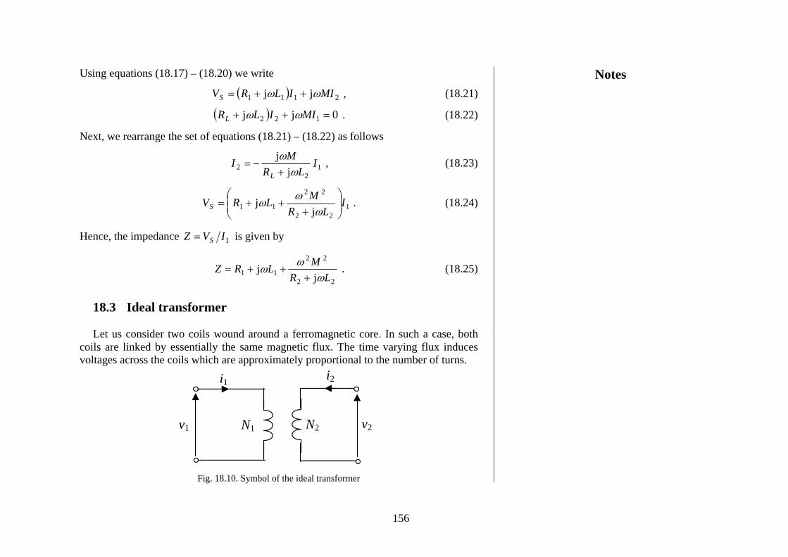
Using equations (18.17) – (18.20) we write
( ) 2111 jj MIILRVS ωω ++= , (18.21)
( ) 0jj 122 =++ MIILRL ωω . (18.22)
Next, we rearrange the set of equations (18.21) – (18.22) as follows
12
2 jj I
LRMI
L ωω+
−= , (18.23)
122
22
11 jj I
LRMLRVS ⎟⎟
⎠
⎞⎜⎜⎝
⎛
+++=
ωωω . (18.24)
Hence, the impedance 1IVZ S= is given by
22
22
11 jj
LRMLRZω
ωω+
++= . (18.25)
18.3 Ideal transformer
Let us consider two coils wound around a ferromagnetic core. In such a case, both
coils are linked by essentially the same magnetic flux. The time varying flux induces voltages across the coils which are approximately proportional to the number of turns.
v2 N1
i2 i1
v1 N2
Fig. 18.10. Symbol of the ideal transformer
Notes
156
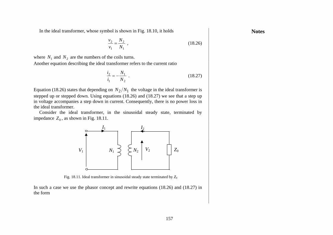
In the ideal transformer, whose symbol is shown in Fig. 18.10, it holds
1
2
1
2
NN
vv
= , (18.26)
where and are the numbers of the coils turns. 1N 2NAnother equation describing the ideal transformer refers to the current ratio
2
1
1
2
NN
ii
−= . (18.27)
Equation (18.26) states that depending on 12 NN the voltage in the ideal transformer is stepped up or stepped down. Using equations (18.26) and (18.27) we see that a step up in voltage accompanies a step down in current. Consequently, there is no power loss in the ideal transformer.
Consider the ideal transformer, in the sinusoidal steady state, terminated by impedance , as shown in Fig. 18.11. 0Z
Z0 V2 N1
I2 I1
V1 N2
Fig. 18.11. Ideal transformer in sinusoidal steady state terminated by Z0
In such a case we use the phasor concept and rewrite equations (18.26) and (18.27) in the form
Notes
157
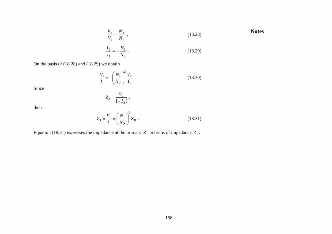
1
2
1
2
NN
VV
= , (18.28)
2
1
1
2
NN
II
−= . (18.29)
On the basis of (18.28) and (18.29) we obtain
2
22
2
1
1
1
IV
NN
IV
⎟⎟⎠
⎞⎜⎜⎝
⎛−= . (18.30)
Since
( )2
20 I
VZ−
= ,
then
0
2
2
1
1
11 Z
NN
IV
Z ⎟⎟⎠
⎞⎜⎜⎝
⎛== . (18.31)
Equation (18.31) expresses the impedance at the primary in terms of impedance . 1Z 0Z
Notes
158

19. Three-phase systems
19.1 Introduction Three-phase systems are commonly used in the generation, transmission and
distribution of electric power. Power in a three-phase system is constant rather than pulsating and three-phase motors start and run much better than single-phase motors. A three-phase system is a generator-load pair in which the generator produces three sinusoidal voltages of equal amplitude and frequency but differing in phase by 120° from each other.
The phase voltages , and ( )tva ( )tvb ( )tvc are as follows
( )( ) ,tVv
tVv
tVv
mc
mb
ma
240cos
120cos
cos
−=
−=
=
ω
ω
ω
(19.1)
whereas the corresponding phasors are
.VV
VV
VV
mc
mb
ma
240j
120j
e
e−
−
=
=
=
(19.2)
A three-phase system is shown in Fig 19.1. In a special case, all impedances are identical
ZZZZ cba === . (19.3)
Such a load is called a balanced load and is described by equations
ZV
IZ
VI
ZV
I cc
bb
aa === .
Notes
159

In
Ia Za Va
Ic Zc Vc
Ib Zb Vb
Fig. 19.1. Four-wire, three-phase system
Using KCL, we have
( )cbacban VVVZ
IIII ++=++=1 , (19.4)
where
( ) .VV
VVVV
mm
mcba
023j
21
23j
211240jsin240cos120jsin120cos1
ee1 240j120j
=⎟⎟⎠
⎞⎜⎜⎝
⎛+−−−=−+−+=
=⎟⎠⎞⎜
⎝⎛ ++=++ −−
Setting the above result into (19.4), we obtain
0=nI . (19.5)
Since the current flowing though the fourth wire is zero, the wire can be removed (see Fig. 19.2). The system of connecting the voltage sources and the load branches, as depicted in Fig. 19.2, is called a Y-system or a star system. Point n is called the neutral point of the generator and point n′ is called the neutral point of the load.
Notes
160
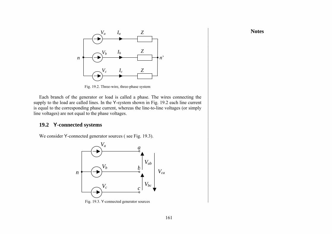
n’ n
Ia Z Va
Ic Z Vc
Ib Z Vb
Fig. 19.2. Three-wire, three-phase system
Each branch of the generator or load is called a phase. The wires connecting the
supply to the load are called lines. In the Y-system shown in Fig. 19.2 each line current is equal to the corresponding phase current, whereas the line-to-line voltages (or simply line voltages) are not equal to the phase voltages.
19.2 Y-connected systems
We consider Y-connected generator sources ( see Fig. 19.3).
Vca
c Vbc
Vab
n
a Va
Vc
bVb
Fig. 19.3. Y-connected generator sources
Notes
161
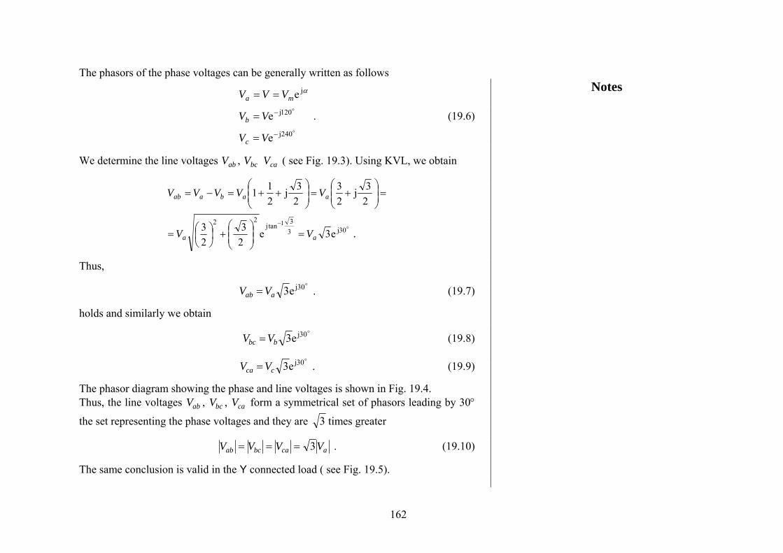
The phasors of the phase voltages can be generally written as follows
. (19.6) 240j
120j
j
e
e
e
−
−
=
=
==
VV
VV
VVV
c
b
maα
We determine the line voltages , ( see Fig. 19.3). Using KVL, we obtain abV bcV caV
.VV
VVVVV
aa
aabaab
30j33tanj
22
e3e23
23
23j
23
23j
211
1
=⎟⎟⎠
⎞⎜⎜⎝
⎛+⎟
⎠⎞
⎜⎝⎛=
=⎟⎟⎠
⎞⎜⎜⎝
⎛+=⎟⎟
⎠
⎞⎜⎜⎝
⎛++=−=
−
Thus,
30je3aab VV = . (19.7)
holds and similarly we obtain
30je3bbc VV = (19.8)
30je3cca VV = . (19.9)
The phasor diagram showing the phase and line voltages is shown in Fig. 19.4. Thus, the line voltages , , form a symmetrical set of phasors leading by 30°
the set representing the phase voltages and they are abV bcV caV
3 times greater
acabcab VVVV 3=== . (19.10)
The same conclusion is valid in the Y connected load ( see Fig. 19.5).
Notes
162

Vc
Vbc Vb
30° Va
Vab
30°
30°
Vca
Fig. 19.4. Phasor diagram
Va
c
b
a
Vbc
Vb Vc
Zc=Z
Za=Z
Zb=Z
Vab
Vca
Fig. 19.5. Y-connected load
Notes
163
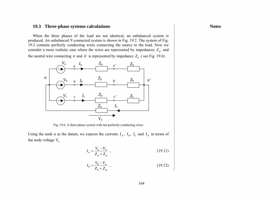
19.3 Three-phase systems calculations
When the three phases of the load are not identical, an unbalanced system is produced. An unbalanced Y-connected system is shown in Fig. 19.2. The system of Fig. 19.2 contains perfectly conducting wires connecting the source to the load. Now we consider a more realistic case where the wires are represented by impedances and the neutral wire connecting and
pZn n′ is represented by impedance ( see Fig. 19.6). nZ
c
b
a
Vn
Zn
c’
a’
b’Zp
Zp
Zp
In
n’ n
Ia Za Va
Ic Zc Vc
Ib Zb Vb
Fig. 19.6. A three-phase system with not perfectly conducting wires
Using the node n as the datum, we express the currents , , and in terms of the node voltage
aI bI cI nI
nV
pa
naa ZZ
VVI
+−
= , (19.11)
pb
nbb ZZ
VVI+−
= , (19.12)
Notes
164

pc
ncc ZZ
VVI+−
= , (19.13)
n
nn Z
VI = . (19.14)
Hence, we obtain the node equation
0=+−
−+−
−+−
−pc
nc
pb
nb
pa
na
n
n
ZZVV
ZZVV
ZZVV
ZV .
Solving this equation for we have nV
pcpbpan
pc
c
pb
b
pa
a
n
ZZZZZZZ
ZZV
ZZV
ZZV
V
++
++
++
++
++
+=
1111 . (19.15)
The above relationships enable us to formulate a method for the analysis of three-phase systems. The method consists of three steps as follows: ( i ) Determine using (19.15). nV( ii ) Calculate the currents , , and applying (19.11) - (19.14). aI bI cI nI( iii ) Find the phase and line voltages using Kirchhoff’s and Ohm’s laws. When the neutral wire is removed, the system contains three connecting wires and is called a three-wire system. In such a case, we set ∞→nZ into (19.15)
pcpbpa
pc
c
pb
b
pa
a
n
ZZZZZZ
ZZV
ZZV
ZZV
V
++
++
+
++
++
+=
111 . (19.16)
Notes
165

The balanced system can be considered as a special case of the unbalanced system, where ZZZZ cba === . Using (19.16), we obtain
( )
03
1
=
+
+++
=
p
cbap
n
ZZ
VVVZZ
V . (19.17)
Consequently, the relationships (19.11)-(19.13) reduce to
p
aa ZZ
VI
+= , (19.18)
p
bb ZZ
VI
+= , (19.19)
p
cc ZZ
VI
+= . (19.20)
Since and , we have and . 120je−= ab VV 240je−= ac VV 120je−= ab II 240je−= ac IIHence, we need to calculate onlyaI using (19.18), which can be executed applying the one-phase circuit, described by equation (19.18), shown in Fig. 19.7.
n’
aV ′
n
Z
Zp Ia Va
Fig. 19.7. One-phase circuit
This means that the analysis of a balanced three-phase system can be reduced to the analysis of one-phase system depicted in Fig. 19.7.
Notes
166
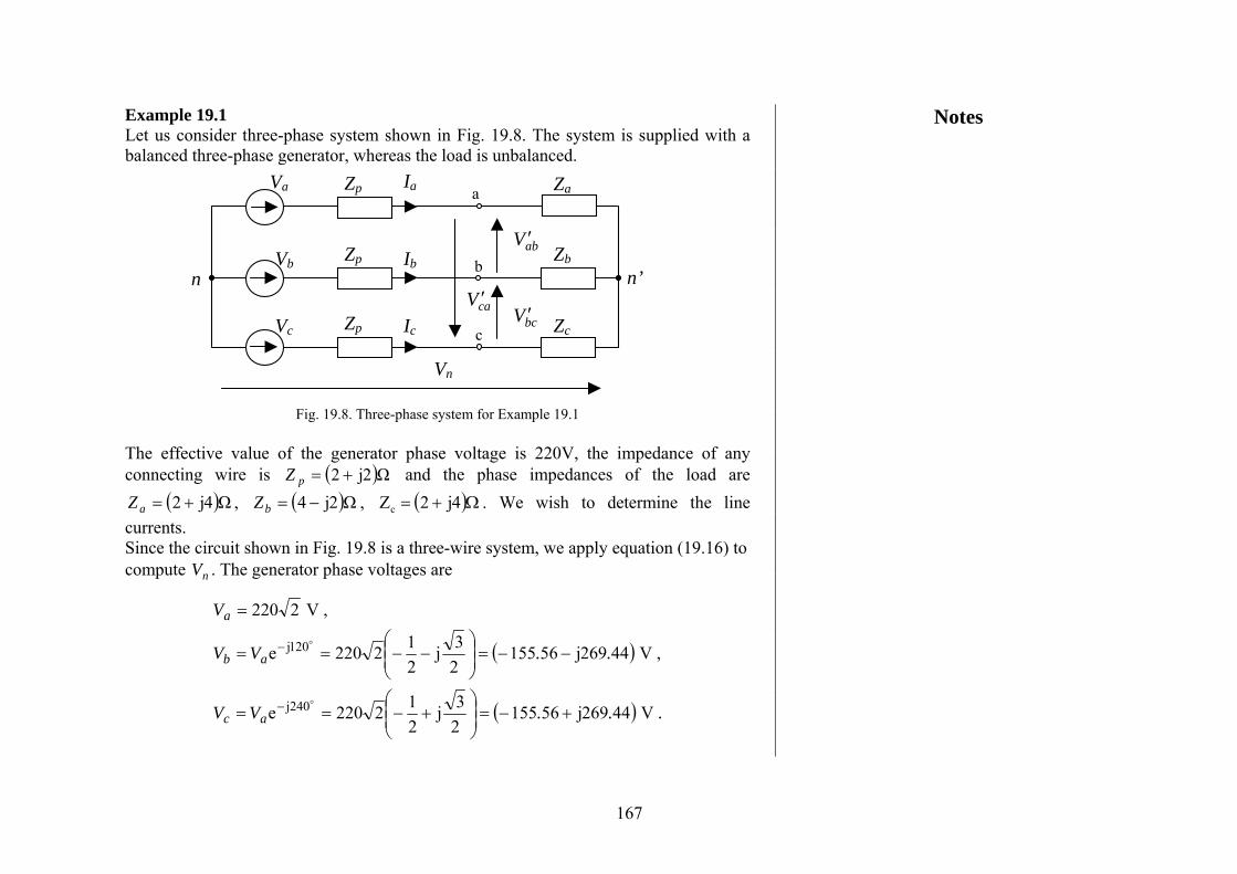
Example 19.1 Let us consider three-phase system shown in Fig. 19.8. The system is supplied with a balanced three-phase generator, whereas the load is unbalanced.
c
a
bZp
Zp
Zp
Vn
caV ′bcV ′
abV ′
n’ n
Ia Za Va
Ic Zc Vc
Ib Zb Vb
Fig. 19.8. Three-phase system for Example 19.1
The effective value of the generator phase voltage is 220V, the impedance of any connecting wire is ( ) and the phase impedances of the load are
( )Ω2j2 +=pZ
Ω4j2 +=aZ , , ( )Ω2j4 −=bZ ( )Ω+= 4j2Zc . We wish to determine the line currents. Since the circuit shown in Fig. 19.8 is a three-wire system, we apply equation (19.16) to compute . The generator phase voltages are nV
( )
( ) ...VV
..VV
V
ac
ab
a
V44269j5615523j
212220e
,V44269j5615523j
212220e
,V2220
240j
120j
+−=⎟⎟⎠
⎞⎜⎜⎝
⎛+−==
−−=⎟⎟⎠
⎞⎜⎜⎝
⎛−−==
=
−
−
Notes
167

Using (19.16), we find
( ) ( )
( ) ...
....
Vn V261j597
6j41
61
6j41
6j444269j56155
644269j56155
6j42220
−=
+++
+
++−
+−−
++
=
Next, we compute the line currents using (19.11) – (19.13)
( )
( )
( ) .......ZZVV
I
......ZZVV
I
....ZZVV
I
pc
ncc
pb
nbb
pa
naa
A6354j68182j24j2
261j59744269j56155
,A7034j18422j22j4
261j59744269j56155
,A9419j49232j24j2
261j5972220
+=+++
+−+−=
+−
=
−−=++−
+−−−=
+−
=
−=++++−
=+−
=
19.4 Power in three-phase circuits
In balanced systems, the average power consumed by each load branch is the same
and given by
φcoseffeffav IVP~ = , (19.21)
where is the effective value of the phase voltage, is the effective value of the phase current and
effV effIφ is the angle of the impedance. The total average power consumed
by the load is the sum of those consumed by each branch, hence, we have
φcos33 effeffavav IVP~P == . (19.22)
In balanced Y systems, the phase current has the same effective value as the line current ( )
Leffeff II = , whereas the line voltage has the effective value ( )LeffV which is
Notes
168

3 times greater than the effective value of the phase voltage, ( ) effLeff VV 3= . Hence, using (19.22), we obtain
( ) ( ) ( ) ( ) φφ cos3cos
33
LeffLeffLeffLeff
av IVIV
P == . (19.23)
Similarly, we derive the reactive power
( ) ( ) φsin3LeffLeffx IVP = . (19.24)
In unbalanced systems, we add the powers of each phase
( ) ( ) ( ) ( ) ( ) ( ) cceffceffbbeffbeffaaeffaeffav IVIVIVP φφφ coscoscos ++= (19.25)
( ) ( ) ( ) ( ) ( ) ( ) cceffceffbbeffbeffaaeffaeffx IVIVIVP φφφ sinsinsin ++= . (19.26)
In order to measure the average power in a three-phase Y-connected load, we use three wattmeters connected as shown in Fig. 19.9. The reading of the ideal wattmeter W1 is
( ) ( ) ( ) ( ) ( ) aaaeffaeffaamamaaW PIVIVIVP ==== ∗ φφ coscos21Re
21
1 .
Similarly, W2 and W3 measure the average power of the load branch b and c, respectively. Thus, the sum of the three readings will give the total average power. This method of the average power measurement is valid for both balanced and unbalanced Y-connected loads. Note that in the case of a balanced Y-connected load all three readings are identical and therefore, we use only one wattmeter.
For measuring average power in a three-phase three-wire system, we can use a method applying two wattmeters. In this method two wattmeters are connected by choosing any one line as the common reference for the voltage coils of the wattmeters. The current coils are connected in series with the other two lines ( see Fig. 19.10) and the asterisk terminals of each wattmeter are short-circuited ( see Fig. 19.10).
Notes
169

n’
*
*
*
*
*
*
i c’
b’
a’
Vc
Vb
Zb
Ia Za
Va
Zc
Ib
W2
W1
W3
Fig. 19.9. Three-wattmeter measurement system
*
*
*
*
c Vbc
Vac b
a Ia
Ic
Ib LoadW2
W1
Fig. 19.10. Two-wattmeter measurement system
Notes
170

The indications of the wattmeters are
( )∗= aacW IVP Re21
1 , (19.27)
( )∗= bbcW IVP Re21
2 . (19.28)
The Y-connected load is shown in Fig. 19.11.
c Vbc
Vac b
a
Vc
Vb
Zb
Ia
Za
Va
Ic
Zc
Ib
Fig. 19.11. Y-connected load
Since caac VVV −= and cbbc VVV −= , we obtain
( )( ) ( )
( )( ) ( ) .IVIVIVVP
,IVIVIVVP
bcbbbcbW
acaaacaW
∗∗∗
∗∗∗
−=−=
−=−=
Re21Re
21
Re21Re
21
2
1
The sum of and gives 1WP
2WP
( )[ ]∗∗∗∗ +−+=+ bacbbaaWW IIVIVIVPP Re21
21 . (19.29)
Notes
171

The currents , , satisfy KCL aI bI cI
0=++ cba III . Hence, it holds , 0=++ ∗∗∗
cba IIIor . (19.30) 0=−=+ ∗∗∗
cba III
Substituting (19.30) into (19.29) we have
[ ] avccbbaaWW PIVIVIVPP =++=+ ∗∗∗Re21
21 . (19.31)
Equation (19.31) says that the sum of the two wattmeters readings in a Y-connected system equals the total average power consumed by the load.
Let us consider a balanced Y-connected load and calculate the instantaneous power delivered by the generator to the load
( ) ( ) ( ) ( ) ( ) ( ) ( )titvtitvtitvtp ccbbaa ++= , (19.32) where
( )( ) ( )( ) ( ) ,tVtv
,tVtv
,tVtv
mc
mb
ma
240cos
120cos
cos
−=
−=
=
ω
ω
ω
(19.33)
and
( ) ( )( ) ( )( ) ( ) ,tIti
,tIti
,tIti
mc
mb
ma
φω
φω
φω
−−=
−−=
−=
240cos
120cos
cos
(19.34)
where ( )tva , ( )tvb , are the voltages of the load branches, ( )tvc ( )tia , ( )tib , are the currents of the load branches and
( )tic
φ is the angle of the load impedance. We substitute (19.33)-( 19.34) in (19.32)
Notes
172

( ) ( ) ( ) ( )
( ) ( )]240cos240cos
120cos120coscos[cos
φωω
φωωφωω
−−−+
+−−−+−=
tt
ttttIVtp mm
and use the trigonometric identity
( ) ( )[ ]yxyxyx ++−=⋅ coscos21coscos ,
finding
( ) ( ) ( ) ( )[ ]φωφωφωφ −−+−−+−+= 4802cos2402cos2coscos321 tttIVtp mm .
Since
( ) ( ) ( ) ,ttt 04802cos2402cos2cos =−−+−−+− φωφωφω
we obtain
( ) aveffeffmm PIVIVtp === φφ cos3cos23 . (19.35)
Thus, the total instantaneous power ( )tp delivered by a three-phase generator to the balanced load is constant and equals the average power consumed by the load.
Notes
173

Reference books
[1] Chua L.O., Desoer C.A., Kuh E.S.: Linear and Nonlinear Circuits. McGraw-Hill, Inc., 1981.
[2] Cook N.P.: Electronics. A Complete Course. Pearson Education Inc., 2004.
[3] Dorf R.C.: Introduction to Electric Circuits. J. Wiley & Sons Ltd., 1989. [4] Dorf R.C.: The Electrical Engineering Handbook. CRC Press., 1997. [5] Madhu S.: Linear Circuit Analysis. Prentice-Hall, Inc., 1988. [6] Smith R.J.: Circuits, Devices, and Systems. J. Wiley & Sons, 1984.
174