ELDO Tutorial
29
Simulation for an Inverter Circuit Using the Design Architect-IC (DA-IC) Santa Clara University Department of Electrical Engineering Revised by Arpita Sharan Under Guidance of Dr Samiha Mourad & Dr Shoba Krishnan Date of Last Revision: October 3, 2006 “All logos and trademarks are the property of their respective owners. Mentor and Mentor Graphics are registered trademarks of Mentor Graphics Corporation, 8005 SW Boeckman Road , Wilsonville , OR 97070-7777 .” Disclaimer - “Information is provided ‘as is’ without warranty of any kind. No statement is made and no attempt has been made to examine the information, either with respect to operability, origin, authorship, or otherwise. Please use this information at your own risk. We recommend using it on a copy of your data to be sure you understand what it does under your conditions. Keep your master intact until you are satisfied with the use of this information within your environment.” Copyright©2006
-
Upload
vinit-patel -
Category
Documents
-
view
95 -
download
0
description
Analog
Transcript of ELDO Tutorial

Simulation for an Inverter Circuit Using
the Design Architect-IC (DA-IC)
Santa Clara University
Department of Electrical Engineering
Revised by Arpita Sharan Under Guidance of Dr Samiha Mourad & Dr Shoba Krishnan Date of Last Revision: October 3, 2006
“All logos and trademarks are the property of their respective owners. Mentor and Mentor Graphics are registered trademarks of Mentor Graphics Corporation, 8005 SW Boeckman Road , Wilsonville , OR 97070-7777 .”
Disclaimer - “Information is provided ‘as is’ without warranty of any kind. No statement is made and no attempt has been made to examine the information, either with respect to operability, origin, authorship, or otherwise. Please use this information at your own risk. We recommend using it on a copy of your data to be sure you understand what it does under your conditions. Keep your master intact until you are satisfied with the use of this information within your environment.”
Copyright©2006

Table of Contents
1. Objective .......................................................................................................................... 4
2. Basic Test Circuit Creation .............................................................................................. 5
Adding Instance to the test circuit .................................................................................. 5
Setting up the simulation parameters .............................................................................. 7
Setting up the simulator / Viewer .................................................................................... 8
2. DC Analysis ................................................................................................................... 10
Editing and simulating the test circuit .......................................................................... 10
Setting up the simulation parameters ............................................................................. 11
Executing the simulation setup ...................................................................................... 13
Viewing the results using EZWave viewer ................................................................... 13
Printing the plots: ........................................................................................................... 14
3. DC Operating Point Analysis ........................................................................................ 16
Editing and simulating the test circuit .......................................................................... 16
Setting up the simulation parameters ............................................................................. 16
Viewing the results using EZWave viewer ................................................................... 17
Power consumption of the circuit .................................................................................. 18
4. Transient Analysis ......................................................................................................... 20
Editing and simulating the test circuit .......................................................................... 20
Setting up the simulation parameters ............................................................................. 21
Setting up the signals to be probed ................................................................................ 22
Executing the simulation setup ...................................................................................... 23
Viewing the results using EZWave viewer ................................................................... 23
5. AC Analysis ................................................................................................................... 26
Editing and simulating the test circuit ........................................................................... 26
Setting up the simulation parameters ............................................................................. 27
Setting up the signals to be probed ................................................................................ 28
Copyright©2006

Executing the simulation setup ..................................................................................... 28
Viewing the results using EZWave viewer ................................................................... 28
Copyright©2006

1. Objective
This Tutorial contains a step-by-step procedure for simulating an inverter circuit in the Mentor Graphics Design Architect tool. It covers DC Analysis, Transient Analysis, DC Operating Point Analysis and AC Analysis simulation of the inverter circuit.
This tutorial assumes that the schematic of the inverter is already created. For help with creating schematic and symbol, please refer to Schematic Entry tutorial for Inverter Circuits.
Copyright©2006

2. Basic Test Circuit Creation
Open icstudio from the command prompt as mentioned in the Schematic Entry tutorial
Create a new view in the created library (Demo_Inverter) and name it as test_inverter with view type as Schematic. We will use this sheet to create basic test circuit required for the simulations.
Adding Instance to the test circuit
A new schematic entry sheet opens in DA-IC. In this test_inverter sheet, i. Add an inverter symbol (that you generated in the schematic entry tutorial) click
Add Instance from schematic_edit palette on RHS. ii. In the Choose Symbol popup window, click Browse, navigate and select inverter
and click OK. Place this symbol of the inverter in the sheet as shown in the figure below.
Copyright©2006

iii. Add a PORTIN, PORTOUT, VDD and Ground from Generic Libiv. Name the ports as INPUT & OUTPUT respectively and wire them to the IN and
OUT pins of the inverter symbol as shown in the figure.v. Add a DC source by selecting IC_Library Sources Library DC.
vi. Highlight the DC source, right click mouse, PropertiesEdit to modify the voltage value of the source from 1V to 3.3V.
vii. Connect the positive node of the DC source to VDD symbol and negative terminal to the Ground symbol. The circuit should look like as shown in the figure below.
Copyright©2006

viii. Click Check & Save the sheet. And then click on simulation from the schematic_edit palette on the RHS to enter the simulation mode. A popup window appears with a Warning message that the schematic will be closed. Click OK to accept default options.
Setting up the simulation parameters
In the simulation mode (schematic_sim palette), Click the right mouse button Lib/Temp/Inc Library. Type /opt/mentor-2004.3/sol/adk2_5/technology/ic/models/tsmc035.mod in
Library path box and click OK. This includes the TSMC0.35 micron BSIM model for the simulations.
The screen now would look like the figure included below
Copyright©2006

Setting up the simulator / Viewer
In the simulation mode (schematic_sim palette), Click Session -> Simulator / Viewer. Select Eldo under Simulator and EZwave under Viewer and click OK.
Copyright©2006

Click on check & save and then click on end simulation to get back in schematic_edit mode.
Copyright©2006

2. DC Analysis
For DC analysis, we sweep the input voltage from 0V to 3.3V and view its effect on the output.
Editing and simulating the test circuit
1) Open the test_inverter sheet that you had created with the symbol of your inverter and make sure that you are in schematic_edit mode.
2) Add a DC voltage source between the INPUT pin and Ground as shown in the following figure. Name this source as VIN. (Note that the value of the DC voltage source is 1V, by default. For DC analysis, this value does not matter and so you can leave it as it is!)
Copyright©2006
3) Click Check & save the sheet and then enter the simulation mode by clicking on simulation from the schematic_edit palette on RHS. Click OK to accept default options in the Warning popup window appeared.
Setting up the simulation parameters
On the schematic_sim palette: Click on Lib/Temp/Inc Library to make sure that
/opt/mentor-2004.3/sol/adk2_5/technology/ic/models/tsmc035.mod appears in library path box and click OK.
Click Setup Analyses. In the Setup Simulation Analysis window that appears, select DC and
click on Setup associated with DC. In the Setup box that appears, select Source and select VIN for Voltage source, put 0 in the start field, 3.3 in the stop field and 0.01 in the step field and then click OK.
Copyright©2006

Select the wires connected to INPUT and OUTPUT pins on the sheet. Click Setup Outputs Save from the Menu Bar. This opens the Set
Plots dialog box. Select Voltage for the Plot type and from Advanced tab select DC for the
Analysis type and click OK. Setup Difference Plot window will appear. Select individually for the
plot type.
Copyright©2006

Executing the simulation setup
On the schematic_sim palette: Click Execute Netlist. This opens up a new window that starts
netlister. Check the netlist created for any errors. If there are any errors, correct them before proceeding further. Else close the window by pressing Enter key.
Click Execute Run Eldo. This starts Eldo in a new shell window and it may take few seconds before the simulation is complete. You may scroll down the window to see the DC simulation results. Press Enter key to close the Shell Window.
Viewing the results using EZWave viewer
Copyright©2006

To view the results of your DC analysis in EZWave, do the following:On the schematic_sim palette:
Click Results -> View Waves. A new window will open with waveform plot as shown below.
Printing the plots:
To Print your waveform: Click File -> Print. Type `laser` for the printer name & Click OK.
Copyright©2006

Copyright©2006

3. DC Operating Point Analysis
In this section, you will find the DC operating point of several nodes in the circuit and look at the transfer function of the input.
Editing and simulating the test circuit
Open the test_inverter sheet that you had created with the symbol of your inverter and make sure that you are in schematic edit mode. The setup is exactly similar to the DC Analysis setup and we will carry out DCOP analysis for input voltage of 1V.
Add a DC voltage source between the INPUT pin and ground as shown in the following figure. Name this source as VIN and make sure that its value is 1V.
Setting up the simulation parameters
On the schematic_sim palette: Click Setup Analyses. Select DCOP in the dialog box that appears, and then
click OK.
Copyright©2006

Click ExecuteNetlist and then Run ELDO.
Viewing the results using EZWave viewer
The next step is to view the results of your simulation run.To see all the DC voltages and currents in your schematic,
Click Results DCOP Add monitor All Nets – Voltages Again click DCOP Add monitor All Pins - Current
Copyright©2006

Current and Voltage values at various nodes will be displayed as shown in the above figure.
Alternately, you can select voltages or current option, if you want to see only voltages or currents.
Power consumption of the circuit
The power consumption of the circuit for the given operating point is calculatedduring the DCOP simulation.
To check it out, Click on Results ASCII Files, right click mouse button View Log. Scroll down in the log window to find the information about the power
consumption as shown in the figure below:
Copyright©2006

Copyright©2006

4. Transient Analysis
In this section, you will provide a pulse at the input and view the input & output waveforms.
Editing and simulating the test circuit Open the test_inverter sheet that you had created with the symbol of your
inverter and make sure that you are in schematic_edit mode. Add a PULSE voltage source between the INPUT pin and Ground as shown in
the following figure. Name this sourse as VIN and change the attributes as:
Initial_value = 0, Pulse_value = 3.3V, Delay = 0, t_rise = 1ns, t_fall = 1ns, Width = 20ns Period = 50ns
( You can use either SHIFT + F7 to change these values one at a time or you may change all the values by first selecting the PULSE voltage source and then Right clicking the mouse to select Properties Edit. Make sure you click Apply after changing each parameter.)
Copyright©2006

Check & save the sheet and then enter the simulation mode by clicking on simulation from the schematic_edit palette on RHS. Click OK to accept default options in the Warning popup window appeared.
Setting up the simulation parameters
On the schematic_sim palette: Click on Lib/Temp/Inc -> Library to make sure that
/opt/mentor-2004.3/sol/adk2_5/technology/ic/models/tsmc035.mod appears in library path box and click OK.
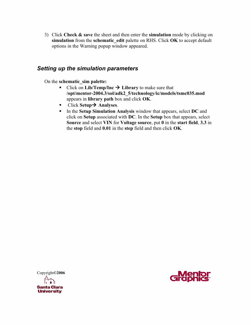
Click Setup -> Analyses. In the Setup Simulation Analysis window that appears, select Transient and click on Setup associated with it.
In the Setup box that appears type 0.1nS in the Output Start Time, 300nS in the Stop Time field and 1nS in Max Time Step field. Then click OK.
Copyright©2006
Setting up the signals to be probed
You need to setup the signals to be plotted and probed in order to view the results after simulation. To view the input and output waveforms of your inverter,
Highlight INPUT and OUTPUT wires on the sheet Click Setup Wave Outputs. Select Voltage for Plot Type; check TRAN for
Analysis type in Advanced and then click OK Setup Difference Plot window will appear select individually for the plot type.
Copyright©2006

Executing the simulation setup
Click Execute -> Netlist Click Execute -> Run ELDO
Viewing the results using EZWave viewer
On the Schematic_sim palette: Select Results ASCII Files from the palette menu to see netlist and log files. Click Results View Waves. Waveform window will appear with both input
and output waveforms mixed into each other as shown in the figure
Copyright©2006

To view the Input & Output waveforms separately, select V (OUTPUT) from Currently Open database test_inverter_eldonet TRAN V (OUTPUT) and click delete and then right click on V (OUTPUT) and click PLOT. Two different plots as shown below will appear.
Copyright©2006

Copyright©2006

5. AC Analysis
In this section, you will run AC analysis and trace and measure your results. In AC Analysis, the input signal is swept over a range of frequencies. First you have to disable the earlier Transient setup that you applied during the transient analysis.
Follow these steps to do AC Analysis on the circuit
Editing and simulating the test circuit
1) Open the test_inverter sheet that you had created with the symbol of your inverter and make sure that you are in schematic_edit mode.
2) Add an AC voltage source between the INPUT pin and Ground as shown in the following figure. Name this source as VIN.
3) Change the value of Mag field to 3.3 V
Copyright©2006

4) Click Check & save the sheet and then enter the simulation mode by clicking on simulation from the schematic_edit palette on RHS. Click OK to accept default options in the Warning popup window appeared.
Setting up the simulation parameters
On the schematic_sim palette: Click Setup -> Analysis. Check AC and click on the Setup box associated with
it. Select the Decade button for Sweep type. For this circuit you will perform an AC sweep of input frequency from 1 to 10G. Enter these values in the Start Freq and Stop Freq respectively. Click OK
Copyright©2006

Setting up the signals to be probed
You need to setup the signals to be plotted and probed in order to view the results after simulation. To view output waveforms of your inverter,
Highlight INPUT and OUTPUT wires Click Setup Output Save Selected components tab. Check AC, select DB-Phase, and then click OK. Setup Difference Plot window will appear select individually for the plot type.
Executing the simulation setup
Click Execute -> Netlist Then click Execute -> Run ELDO.
Viewing the results using EZWave viewer
Select Results -> ASCII Files -> View Log from the palette menu to see netlist. Make sure it does not show any ERROR.
To view the results of your AC analysis, invoke the EZWave viewer by clicking on Results -> View Waves
Copyright©2006

Copyright©2006
Finally I understand this stuff!


![Eldo Ontology For E Learning Design[M Giacomantonio]2](https://static.fdocuments.us/doc/165x107/5490c2aeb47959aa048b47d8/eldo-ontology-for-e-learning-designm-giacomantonio2.jpg)