BSA Electricity Merit Badge Electricity Merit Badge Basic Electricity.
ELCT 871: Advanced Semiconductor Devicesee.sc.edu/personal/faculty/simin/elct871/01...
19
ELCT 871: Advanced Semiconductor Devices
Transcript of ELCT 871: Advanced Semiconductor Devicesee.sc.edu/personal/faculty/simin/elct871/01...

ELCT 871: Advanced
Semiconductor Devices
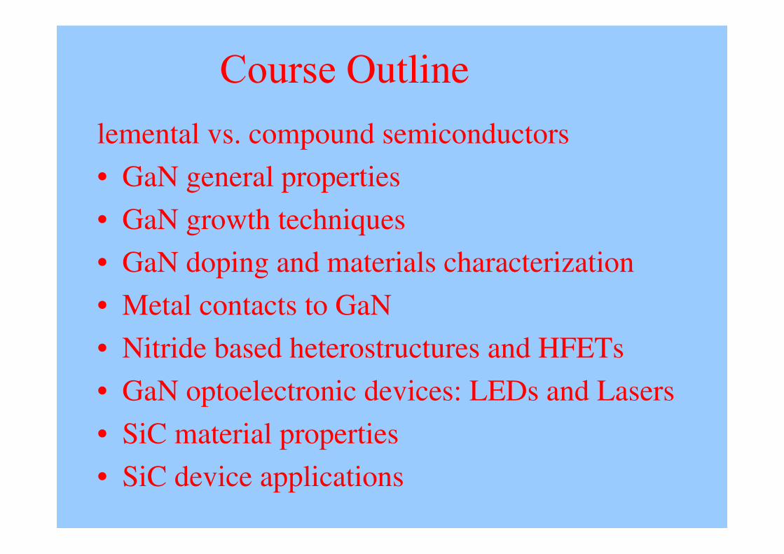
Course Outline
lemental vs. compound semiconductors
• GaN general properties
• GaN growth techniques
• GaN doping and materials characterization
• Metal contacts to GaN
• Nitride based heterostructures and HFETs
• GaN optoelectronic devices: LEDs and Lasers
• SiC material properties
• SiC device applications

Semiconductor electronic devices tree
Semiconductor devices
Elemental semiconductors Compound semiconductors*
Low power
High speed
High power
Low speed
Low power
High speed
High power
High speed
SiC MESFETs
Wide bandgap
Nitride HEMTs
Si and strained
Si MOSFETs,
SiGe HBTs
Power BJT,
IGBTs,
Thyristors etc.
LDMOS
DMOS
High power
High speed
pHEMTs,
HBTs
*Optoelectronic devices : Lasers and LEDs

Lattice constant vs. bandgap for
common semiconductors

Common semiconductors comparison
Properties Si
(----)
GaAs
(AlGaAs/
InGaAs)
InP
(InAlAs/
InGaAs)
4H- SiC
(----)
GaN
(AlGaN/
GaN)
Bandgap (eV) 1.11 1.42 1.35 3.26 3.42
µe (cm2/Vs) 1500 8500
(10000)
5400
(10000)700 900
(2000)
Vsat
(× 107 cm/s)
1 1
(2.1)
1
(2.3)
2 1.5
(2.7)
2DEG density
(cm-2)
NA < 4×10¹² < 4×10¹² NA 1-2 ×10¹³
EB (106 V/cm) 0.3 0.4 0.5 2 3.3
Dielectric
constant
11.8 12.8 12.5 10 9
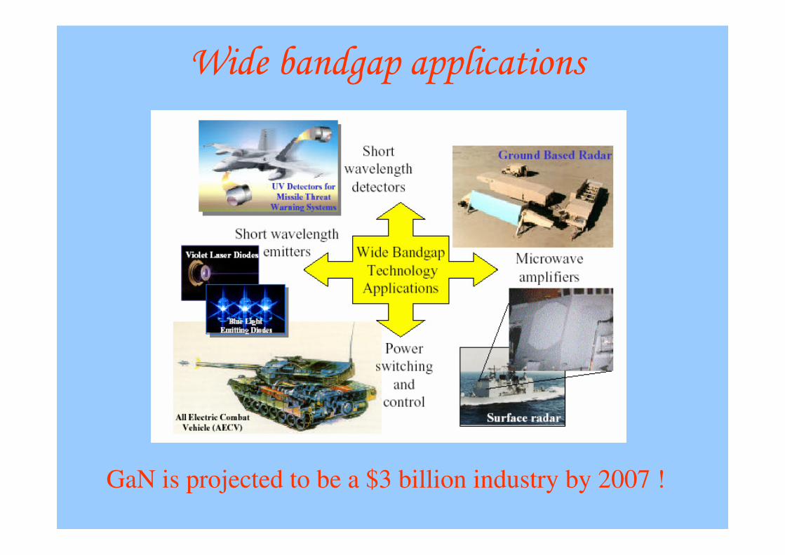
Wide bandgap applications
GaN is projected to be a $3 billion industry by 2007 !
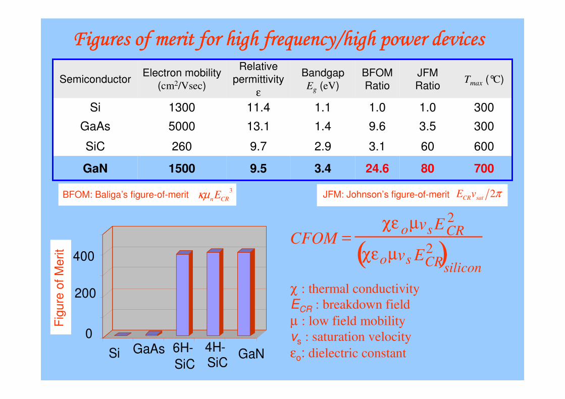
Figures of merit for high frequency/high power devicesFigures of merit for high frequency/high power devicesFigures of merit for high frequency/high power devicesFigures of merit for high frequency/high power devices
7008024.63.49.51500GaN
600603.12.99.7260SiC
3003.59.61.413.15000GaAs
3001.01.01.111.41300Si
Tmax (°C)JFM
Ratio
BFOM
Ratio
BandgapEg (eV)
Relative
permittivity
ε
Electron mobility (cm2/Vsec)
Semiconductor
BFOM: Baliga’s figure-of-merit3
n CREκµ 2CR satE v π
CFOM =χε oµvsECR
2
χεoµvs ECR2( )
silicon
χ : thermal conductivityE
CR: breakdown field
µ : low field mobilityvs : saturation velocity
εo: dielectric constant
0
200
400
Si GaAs 6H-
SiC
4H-SiC
GaN
Fig
ure
of
Merit
JFM: Johnson’s figure-of-merit

Advantages for Nitride Electronic DevicesAdvantages for Nitride Electronic DevicesAdvantages for Nitride Electronic DevicesAdvantages for Nitride Electronic Devices
• High mobility
• High saturation velocity
• High sheet carrier concentration
• High breakdown field
• Wide bandgap ( )
• Growth on SiC substrate
• Chemical inertness
• Good ohmic contacts
• No micropipes
High microwave power,
Power electronic devices
High temperature operation
Holds promise for reliable
device fabrication
Properties Advantages
• SiO2/AlGaN and SiO2/GaN good
quality interfaces
Insulated Gate
transistors possible
kTE
VCiGNNn
2/exp−=

Power densities for AlGaN/GaN HEMTs vs. Time
Highest reported value of power density of 32 W/mm, EDL, April, 2004
0
5
10
15
20
25
30
35
96 98 00 02 04 06
Ou
tpu
t P
ow
er d
ensi
ty (
W/m
m)
Years
Best GaAs device
~1.2 W/mm
Best SiC device ~5.5
W/mm
Field-plated gate used to
enhance breakdown voltage

Size reduction with same output power

Applications in power electronics
Schottky metal Low doped GaN n+ substrate Ohmic metal
VB = Reverse breakdown voltage
EM = Maximum electric field strength at breakdown
ρs = substrate resistivity
Ws = thickness of substrate
A = cross-sectional area
CSMBON RWEVR +⋅+⋅⋅= µε )/4(32 (per unit area)ρs
Advantage: Higher VB for same Ron, and lower Ron for the same VB
( ) [ ]( )FONBFF JARnTAJenkTV ⋅⋅++= ∗∗ φ2/ln/
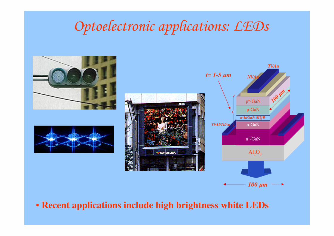
Optoelectronic applications: LEDs
Pd/Ag/Au
Al2O3
n+-GaN
n-GaN
n-InGaN MQW
p-GaN
p+-GaN
Ni/Au
Ti/Au
Ti/Al/Ti/Au
100 µm
t= 1-5 µm
100 µm
• Recent applications include high brightness white LEDs

Nitride based lasers
• Purple - Blue CW Lasers (> 104 hour lifetime easily achieved)
• Blue lasers are used for increasing storage capacities of DVDs
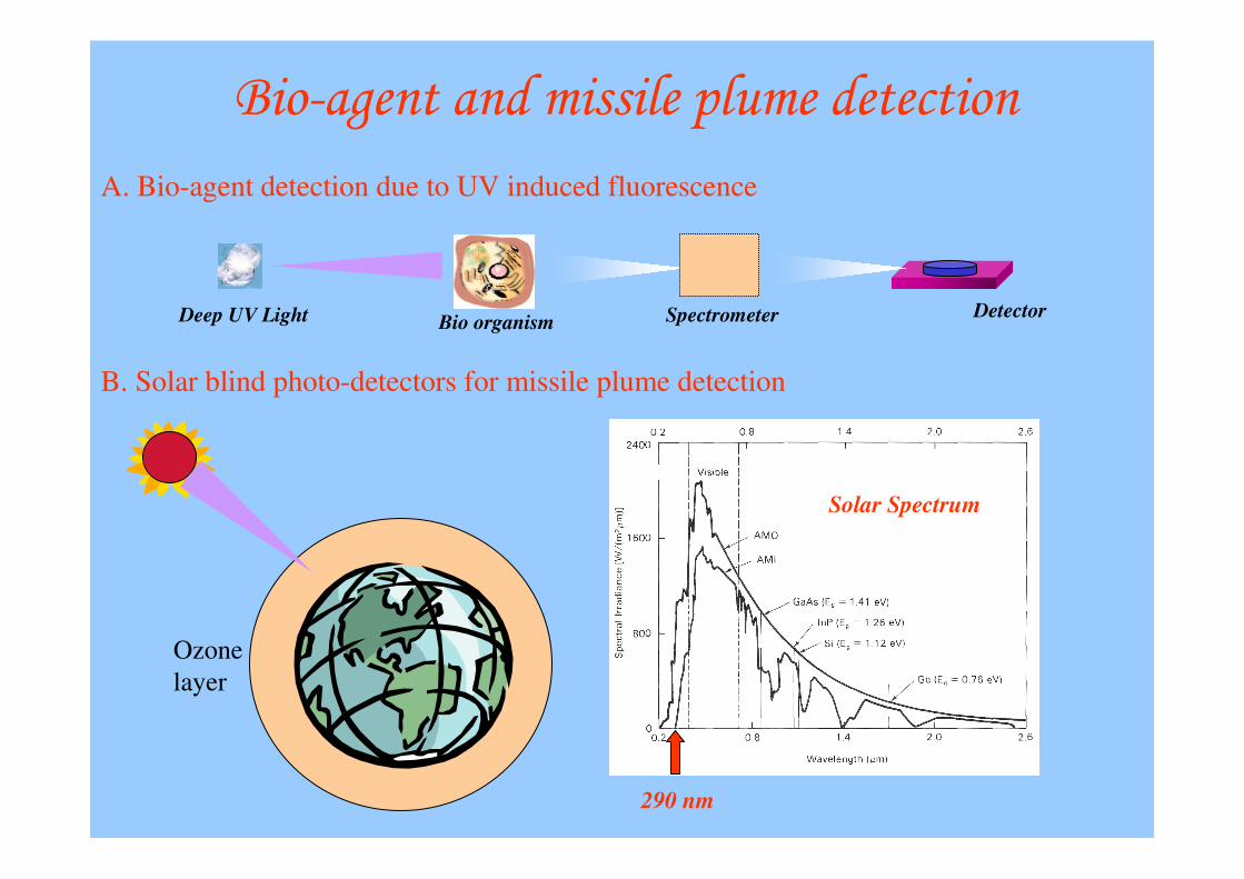
Bio-agent and missile plume detection
Ozone
layer
290 nm
Bio organismDetectorDeep UV Light Spectrometer
Solar Spectrum
A. Bio-agent detection due to UV induced fluorescence
B. Solar blind photo-detectors for missile plume detection
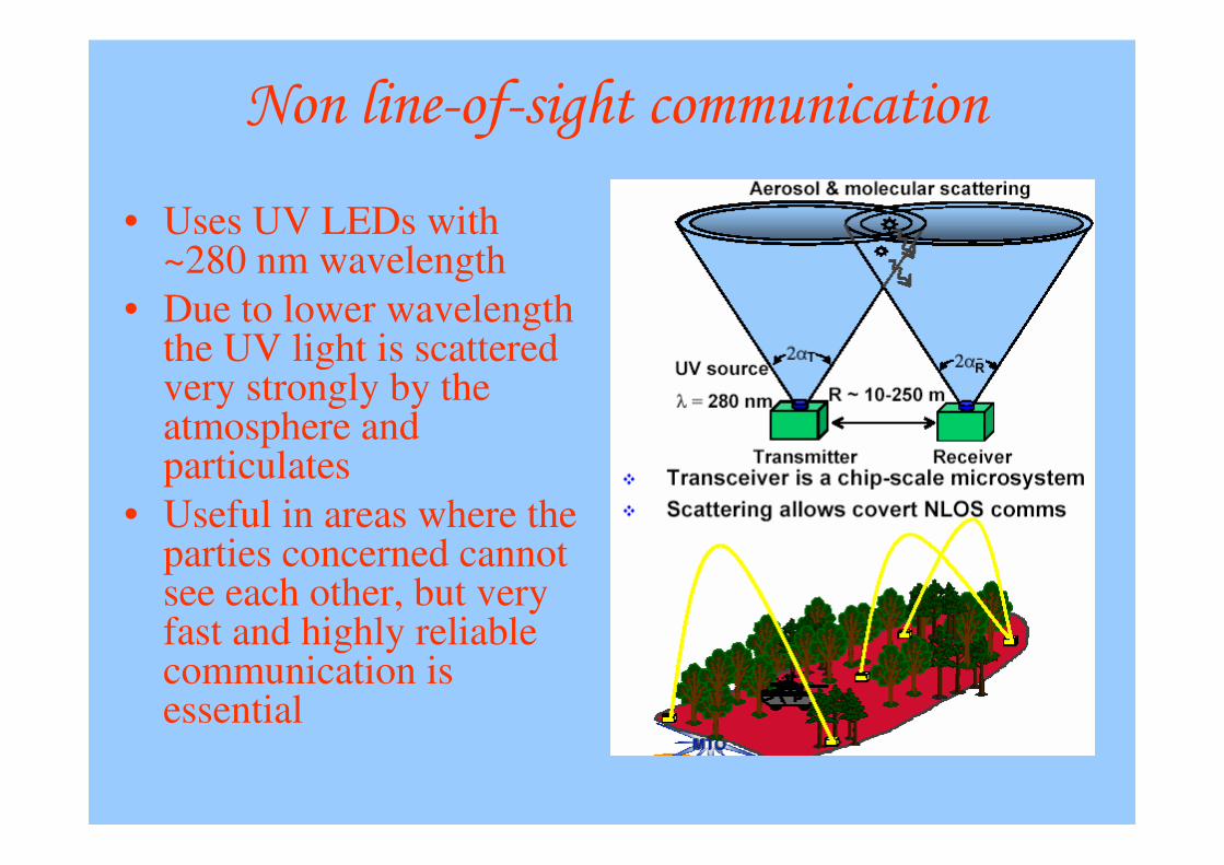
Non line-of-sight communication
• Uses UV LEDs with ~280 nm wavelength
• Due to lower wavelength the UV light is scattered very strongly by the atmosphere and particulates
• Useful in areas where the parties concerned cannot see each other, but very fast and highly reliable communication is essential
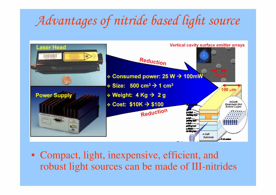
Advantages of nitride based light source
• Compact, light, inexpensive, efficient, and robust light sources can be made of III-nitrides
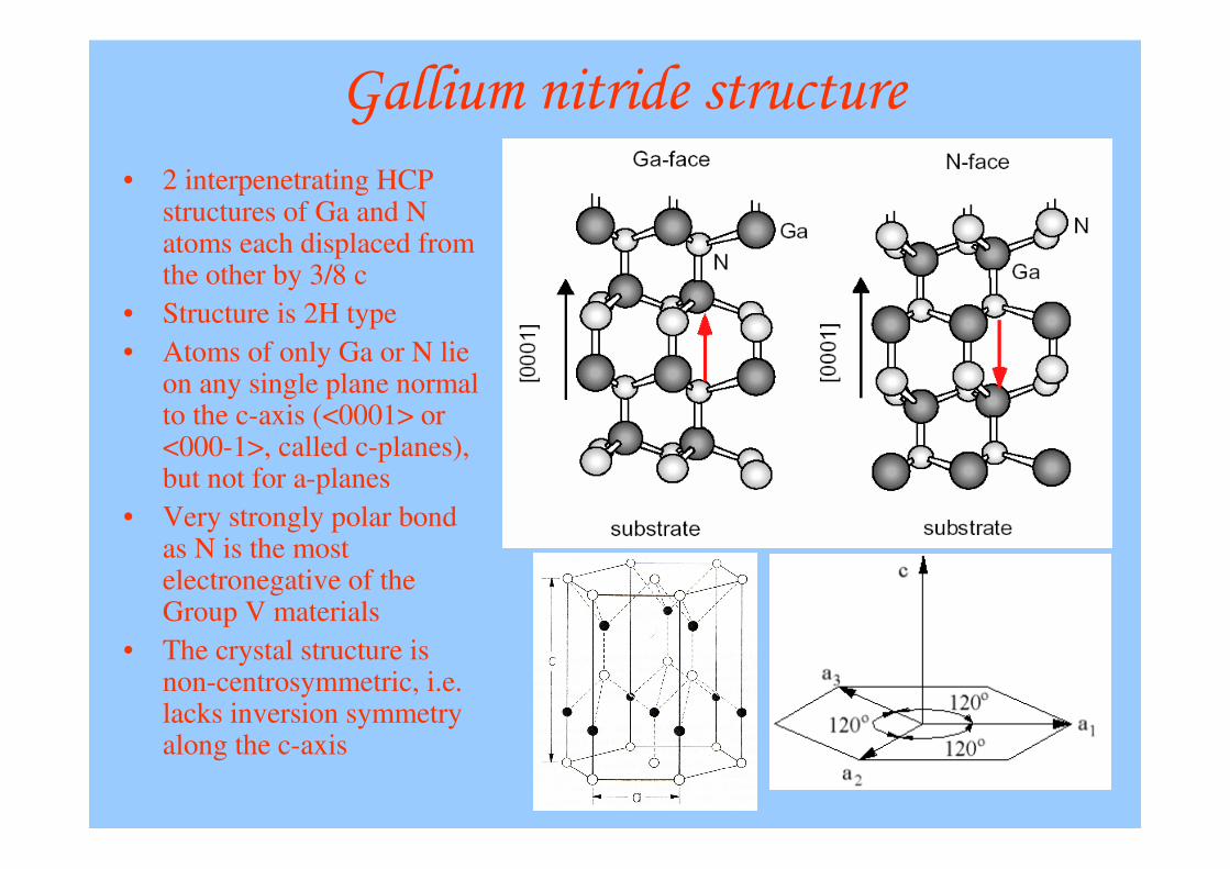
Gallium nitride structure
• 2 interpenetrating HCP structures of Ga and N atoms each displaced from the other by 3/8 c
• Structure is 2H type
• Atoms of only Ga or N lie on any single plane normal to the c-axis (<0001> or <000-1>, called c-planes), but not for a-planes
• Very strongly polar bond as N is the most electronegative of the Group V materials
• The crystal structure is non-centrosymmetric, i.e. lacks inversion symmetry along the c-axis

SiC polytypes
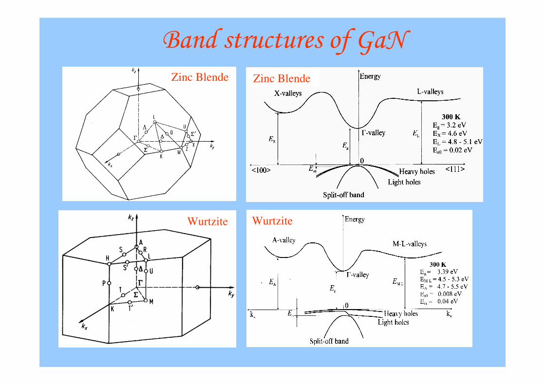
Band structures of GaN
Zinc BlendeZinc Blende
WurtziteWurtzite