Elayampalayam, Tiruchengode 637 205 Programme M.E ...vcenggw.ac.in/pdf/ae/ae_syllabus-2014.pdf ·...
31
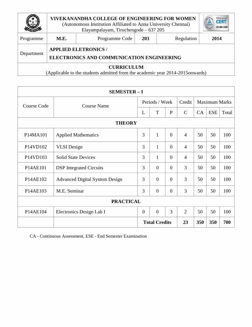
VIVEKANANDHA COLLEGE OF ENGINEERING FOR WOMEN (Autonomous Institution Affiliated to Anna University Chennai) Elayampalayam, Tiruchengode – 637 205 Programme M.E. Programme Code 203 Regulation 2014 Department APPLIED ELETRONICS / ELECTRONICS AND COMMUNICATION ENGINEERING CURRICULUM (Applicable to the students admitted from the academic year 2014-2015onwards) SEMESTER – I Course Code Course Name Periods / Week Credit Maximum Marks L T P C CA ESE Total THEORY P14MA101 Applied Mathematics 3 1 0 4 50 50 100 P14VD102 VLSI Design 3 1 0 4 50 50 100 P14VD103 Solid State Devices 3 1 0 4 50 50 100 P14AE101 DSP Integrated Circuits 3 0 0 3 50 50 100 P14AE102 Advanced Digital System Design 3 0 0 3 50 50 100 P14AE103 M.E. Seminar 3 0 0 3 50 50 100 PRACTICAL P14AE104 Electronics Design Lab I 0 0 3 2 50 50 100 Total Credits 23 350 350 700 CA - Continuous Assessment, ESE - End Semester Examination
Transcript of Elayampalayam, Tiruchengode 637 205 Programme M.E ...vcenggw.ac.in/pdf/ae/ae_syllabus-2014.pdf ·...
VIVEKANANDHA COLLEGE OF ENGINEERING FOR WOMEN(Autonomous Institution Affiliated to Anna University Chennai)
Elayampalayam, Tiruchengode – 637 205
Programme M.E. Programme Code 203 Regulation 2014
DepartmentAPPLIED ELETRONICS /
ELECTRONICS AND COMMUNICATION ENGINEERING
CURRICULUM(Applicable to the students admitted from the academic year 2014-2015onwards)
SEMESTER – I
Course Code Course NamePeriods / Week Credit Maximum Marks
L T P C CA ESE Total
THEORY
P14MA101 Applied Mathematics 3 1 0 4 50 50 100
P14VD102 VLSI Design 3 1 0 4 50 50 100
P14VD103 Solid State Devices 3 1 0 4 50 50 100
P14AE101 DSP Integrated Circuits 3 0 0 3 50 50 100
P14AE102 Advanced Digital System Design 3 0 0 3 50 50 100
P14AE103 M.E. Seminar 3 0 0 3 50 50 100
PRACTICAL
P14AE104 Electronics Design Lab I 0 0 3 2 50 50 100
Total Credits 23 350 350 700
CA - Continuous Assessment, ESE - End Semester Examination

VIVEKANANDHA COLLEGE OF ENGINEERING FOR WOMEN(Autonomous Institution Affiliated to Anna University Chennai)
Elayampalayam, Tiruchengode – 637 205
Programme M.E. Programme Code 203 Regulation 2014
DepartmentAPPLIED ELETRONICS /
ELECTRONICS AND COMMUNICATION ENGINEERING
CURRICULUM(Applicable to the students admitted from the academic year 2014-2015onwards)
SEMESTER – II
Course Code Course NamePeriods / Week Credit Maximum Marks
L T P C CA ESE Total
THEORY
P14AE205Analysis and Design of AnalogIntegrated Circuits
3 0 0 3 50 50 100
P14AE206 Digital Control Engineering 3 0 0 3 50 50 100
P14AE207 Power Electronics 3 0 0 3 50 50 100
P14AE208 Embedded Systems Design 3 0 0 3 50 50 100
Elective – I 3 0 0 3 50 50 100
Elective – II / R&D project withconvener approval
3 0 0 3 50 50 100
PRACTICAL
P14AE209 Electronics Design Lab II 0 0 3 2 50 50 100
Total Credits 20 350 350 700
CA - Continuous Assessment, ESE - End Semester Examination

VIVEKANANDHA COLLEGE OF ENGINEERING FOR WOMEN(Autonomous Institution Affiliated to Anna University Chennai)
Elayampalayam, Tiruchengode – 637 205
Programme M.E. Programme Code 203 Regulation 2014
DepartmentAPPLIED ELETRONICS /
ELECTRONICS AND COMMUNICATION ENGINEERING
CURRICULUM(Applicable to the students admitted from the academic year 2014-2015onwards)
SEMESTER – III
Course Code Course NamePeriods / Week Credit Maximum Marks
L T P C CA ESE Total
THEORY
Elective – III 3 0 0 3 50 50 100
Elective - IV 3 0 0 3 50 50 100
Institute Elective / Elective - V 3 0 0 3 50 50 100
PRACTICAL
P14AE310 Project Stage I 0 0 12 6 50 50 100
Total Credits 15 200 200 400
CA - Continuous Assessment, ESE - End Semester Examination

VIVEKANANDHA COLLEGE OF ENGINEERING FOR WOMEN(Autonomous Institution Affiliated to Anna University Chennai)
Elayampalayam, Tiruchengode – 637 205
Programme M.E. Programme Code 203 Regulation 2014
DepartmentAPPLIED ELETRONICS /
ELECTRONICS AND COMMUNICATION ENGINEERING
CURRICULUM(Applicable to the students admitted from the academic year 2014-2015onwards)
SEMESTER – IV
Course Code Course NamePeriods / Week Credit Maximum Marks
L T P C CA ESE Total
PRACTICAL
P14AE411 Project Stage II 0 0 24 12 50 50 100
Total Credits 12 50 50 100
CA - Continuous Assessment, ESE - End Semester Examination
*Project stage 2 is a continuation of project stage 1

LIST OF ELECTIVES
Course Code Course NamePeriods / Week Credit Maximum Marks
L T P C CA ESE Total
THEORY
P14AEE01 Digital Image Processing 3 0 0 3 50 50 100
P14CSE16 Neural Networks and Its Applications 3 0 0 3 50 50 100
P14AEE02 Robotics 3 0 0 3 50 50 100
P14AEE03 Design and Analysis of Algorithms 3 0 0 3 50 50 100
P14AEE04 Reliability Engineering 3 0 0 3 50 50 100
P14AEE05Electromagnetic Interference andCompatibility in System Design
3 0 0 3 50 50 100
P14VDE04 RF Microelectronics chip design 3 0 0 3 50 50 100
P14AEE06 Hardware Software Co-Design 3 0 0 3 50 50 100
P14VDE01 Physics of Nano electronic Devices I 3 0 0 3 50 50 100
P14AEE07 ASIC Design 3 0 0 3 50 50 100
P14AEE08 Low Power VLSI Design 3 0 0 3 50 50 100
P14AEE09 VLSI Signal Processing 3 0 0 3 50 50 100
P14VDE04 CMOS Analog VLSI Design 3 0 0 3 50 50 100
P14VD210 Foundations of VLSI CAD 3 0 0 3 50 50 100
P14AEE10 High Performance Computer Networks 3 0 0 3 50 50 100
CA - Continuous Assessment, ESE - End Semester Examination

VIVEKANANDHA COLLEGE OF ENGINEERING FOR WOMEN(Autonomous Institution Affiliated to Anna University Chennai)
Elayampalayam, Tiruchengode – 637 205
Programme M.E. Programme Code Regulation 2014
DepartmentVLSI DESIGN , POWER SYSTEMS &APPLIED ELECTRONICS
Semester I
Course Code Course NamePeriods Per Week Credit Maximum Marks
L T P C CA ESE Total
P14MA101 APPLIED MATHEMATICS 3 1 0 4 50 50 100
Objectives
At the end of the course Student would be exposed to fundamental knowledge inOne Dimensional random variables, Testing the hypothesis.
Linear programming, Computational methods in Engineering and Various Queuing models.
Random Variables- Probability Function-Moments-Moment Generating Function & their Properties-Binomial, Poisson, Geometric, Uniform, Exponential Distributions, Testing of Hypothesis, BasicDefinitions:- ( Population, Sampling, Tests of Significance, Testing a Hypothesis, Null Hypothesis,Alternative Hypothesis, Level of Significance, Types of Errors ) – Testing of Hypothesis using : ‘t’-Test ,‘F’-Test , Chi Square Test ( ψ2) - Test for Independence of Attributes & Goodness of Fit. LinearProgramming, Formulation-Graphical solution-Simplex Method -Transportation and Assignment problems.Dynamic Programming-principle of optimality-forward and backward recursion-DP Applications (Cargoloading method)-Problems of dimensionality. Queuing Models, Introduction-Markovian Models: M/M/1:infinite capacity-M/M/C: infinite capacity-M/M/1: finite capacity – M/M/C: finite capacity, Little’sformula.
Total Periods 60
REFERENCES:
1. B.V.Ramana – ‘Higher Engineering Mathematics’, by Tata McGraw Hill Publishing Pvt Ltd – NewDelhi, 2008th Edition.
2. Taha, H.A. “Operations Research: An Introduction, Seventh Edition, Person Education Edition, Asia,New Delhi(2002).
3. Moon,T.K., Sterling,W.C., Mathematical methods and algorithms for signal processing, PearsonEducation,2000
4. Donald Gross and Carl M.Harris, Fundamentals of queuing theory,2nd Edition, john Wiley and Sons,New York(1985)
5. Richard Johnson, Miller & Freund’s Probability and statistics for Engineers,7 th Edition, Prentice-Hallof India, Private Ltd., New Delhi(2007)

VIVEKANANDHA COLLEGE OF ENGINEERING FOR WOMEN(Autonomous Institution Affiliated to Anna University Chennai)
Elayampalayam, Tiruchengode – 637 205
Programme M.E. Programme Code Regulation 2014
DepartmentVLSI DESIGN &APPLIED ELECTRONICS/ ELECTRONICS AND COMMUNICATIONENGINEERING
Semester I
Course Code Course NamePeriods Per Week Credit Maximum Marks
L T P C CA ESE Total
P14VD102 VLSI DESIGN 3 1 0 4 50 50 100
Objectives
To understand the concepts of NMOS and PMOS transistors. To understand the Basic CMOS technology.
To Study the Multiplexers. To understand the concepts of Basics of CMOS testing.
To understand the concepts of digital design with VHDL.
Review of MOS transistor models. CMOS logic families including static, dynamic and dual rail logic.Integrated Circuit Layout: Design Rules, Parasitics. Building blocks: ALU's, FIFO's, counters. VLSI systemdesign: data and control path design, floor planning, Design methodology: Introduction to hardwaredescription languages (VHDL), logic, and circuit and layout verification. Design examples.
Total Periods 60REFERENCES:
1. N. Weste and K. Eshranghian, Principles of CMOS VLSI Design, Addison Wesley. 19852. L. Glaser and D. Dobberpuhl, The Design and Analysis of VLSI Circuits, Addison Wesley, 19853. C. Mead and L. Conway, Introduction to VLSI Systems, Addison Wesley, 19794. J. Rabaey, Digital Integrated Circuits: A Design Perspective, Prentice Hall India, 1997

VIVEKANANDHA COLLEGE OF ENGINEERING FOR WOMEN(Autonomous Institution Affiliated to Anna University Chennai)
Elayampalayam, Tiruchengode – 637 205
Programme M.E. Programme code Regulation 2014
DepartmentVLSI DESIGN &APPLIED ELECTRONICS/ ELECTRONICS AND COMMUNICATIONENGINEERING
Semester I
Course Code Course NamePeriods Per Week Credit Maximum Marks
L T P C CA ESE Total
P14VD103 SOLID STATE DEVICES 3 1 0 4 50 50 100
Objectives To study the Fundamentals of physics. To study the different level of flow in detail.
Electrons in solids, Band theory, Charge carriers in semiconductors, Boltzmann Transport Equation, p-njunctions, Schottky and MIS contacts, Field-effect transistors, Bipolar transistors, Optoelectronic andphotovoltaic devices.
Total Periods 60REFERENCES:
1. Ben.G. Streetman and Sanjay Banerjee, Solid State Electronic Devices, Prentice Hall, 6/E 2005
2. Sze and Ng, Physics of Semiconductor Devices, Wiley-Interscience, 3/E 2006

VIVEKANANDHA COLLEGE OF ENGINEERING FOR WOMEN(Autonomous Institution Affiliated to Anna University Chennai)
Elayampalayam, Tiruchengode – 637 205
Programme M.E. Programme Code 203 Regulation 2014
DepartmentAPPLIED ELECTRONICS /ELECTRONICS AND COMMUNICATIONENGINEERING
Semester I
Course Code Course NamePeriods Per Week Credit Maximum Marks
L T P C CA ESE Total
P14AE101 DSP INTEGRATED CIRCUITS 3 0 0 3 50 50 100
Objectives To study the advanced digital signal processors and IC technologies. To explore the concepts of multi rate signal processing and multi rate filters. To study the complex multipliers and VLSI layouts.
Standard digital signal processors, Application specific IC’s for DSP, DSP systems, DSP system design,Integrated circuit design. MOS transistors, MOS logic, VLSI process technologies Transfer functions, Signalflow graphs, Filter structures, Adaptive DSP algorithms, , FFT-The Fast Fourier Transform Algorithm, Imagecoding, Discrete cosine transforms.FIR filters, FIR filter structures, FIR chips, IIR filters, Specifications of IIR filters, Mapping of analog transferfunctions, Mapping of analog filter structures,, Sampling rate change with a ratio L/M, Multi-rate filters. Finiteword length effects -Parasitic oscillations, Scaling of signal levels, Round-off noise, Measuring round-off noise,Coefficient sensitivity, Sensitivity and noise.DSP system architectures, Standard DSP architecture, Ideal DSP architectures, Multiprocessors and multi-computers, Systolic and Wave front arrays, Shared memory architecture with Bit – serial PEs. Conventionalnumber system, Redundant Number system, Residue Number System, Layout of VLSI circuits, FFT processor,DCT processor and Interpolator as case studies. CORDIC algorithm.
Total Periods 45REFERENCES:
1. Lars Wan hammer, “DSP Integrated Circuits”, Academic press, New York 19992. Oppenheim A.V. et.al, ‘Discrete-time Signal Processing’ Pearson Education,2000
FURTHER READINGS:
1. Emmanuel C. Ifeachor, Barrie W. Jervis, “ Digital signal processing – A practical approach”,Second edition, Pearson education, Asia 2001practical approach”, Second edition, Pearson education, Asia 2001
2. Keshab K.Parhi, ‘VLSI digital Signal Processing Systems design and Implementation’ JohnWiley & Sons, 1999

VIVEKANANDHA COLLEGE OF ENGINEERING FOR WOMEN(Autonomous Institution Affiliated to Anna University Chennai)
Elayampalayam, Tiruchengode – 637 205
Programme M.E. Programme Code 203 Regulation 2014
DepartmentAPPLIED ELECTRONICS /ELECTRONICS ANDCOMMUNICATION ENGINEERING
Semester I
Course Code Course NamePeriods Per Week Credit Maximum Marks
L T P C CA ESE Total
P14AE102 ADVANCED DIGITAL SYSTEMDESIGN
3 0 0 3 50 50 100
Objectives
To provide an in-depth knowledge of synchronous and asynchronous sequentialcircuits analysis and design.
To provide the basics of fault diagnosis and testing algorithms. To study the design of synchronous sequential circuits using PLDs.
To study the design of digital systems using VHDL.Analysis of clocked synchronous sequential circuits and modeling- State diagram, state table, state tableassignment and reduction-Design of synchronous sequential circuits design of iterative circuits-ASM chartand realization using ASM Analysis of asynchronous sequential circuit – flow table reduction-races-stateassignment-transition table and problems in transition table- design of asynchronous sequential circuit-Static, dynamic and essential hazards – data synchronizers – mixed operating mode asynchronous circuits –designing vending machine controller Fault table method-path sensitization method – Tolerance techniques– The compact algorithm – Fault in PLA – Test generation-DFT schemes – Built in self-test Programminglogic device families – Designing a synchronous sequential circuit using PLA/PAL – Realization of finitestate machine using PLD – FPGA –concurrent and sequential statements – packages- Data flow –Behavioral – structural modeling – compilation and simulation of VHDL code –Test bench - Realization ofcombinational and sequential circuits using HDL – Registers – counters – sequential machine – serial adder– Multiplier- Divider – Design of simple microprocessor
Total Periods 45REFERENCES:
1. Charles H.Roth,Jr “Fundamentals of Logic Design” Thomson Learning 2004FURTHER READINGS:
1. Nripendra N Biswas, “Logic Design Theory” Prentice Hall of India,20012. ParagK.Lala, “Fault Tolerant and Fault Testable Hardware Design” B S Publications,20023. ParagK.Lala, “Digital system DesignusingPLD”BSPublications,20034. Charles H Roth Jr.”Digital System Design using VHDL” Thomson learning, 20045. Douglas L.Perry “VHDL programming by Example” Tata McGraw.Hill - 2006

VIVEKANANDHA COLLEGE OF ENGINEERING FOR WOMEN(Autonomous Institution Affiliated to Anna University Chennai)
Elayampalayam, Tiruchengode – 637 205Programme M.E. Programme Code 203 Regulation 2014
DepartmentAPPLIED ELECTRONICS /ELECTRONICS ANDCOMMUNICATION ENGINEERING
Semester I
Course Code Course NamePeriods Per Week Credit Maximum Marks
L T P C CA ESE Total
P14AE104 ELECTRONIC DESIGN LAB I 0 0 3 2 50 50 100
LIST OF EXPERIMENTS:
1. System design using PIC Microcontroller.
2. Implementation of Adaptive Filters, periodogram and multistage multirate system in DSP Processor
3. Simulation of QMF using Simulation Packages
4. Modeling of Sequential Digital system using VHDL.
5. Modeling of Sequential Digital system using Verilog.
6. Design and Implementation of ALU using FPGA.
7. Simulation of NMOS and CMOS circuits using SPICE.
8. System design using 16- bit Microprocessor.
TOTAL PERIODS:60 HOURS

VIVEKANANDHA COLLEGE OF ENGINEERING FOR WOMEN(Autonomous Institution Affiliated to Anna University Chennai)
Elayampalayam, Tiruchengode – 637 205
Programme M.E. Programme Code 203 Regulation 2014
DepartmentAPPLIED ELECTRONICS /ELECTRONICS ANDCOMMUNICATION ENGINEERING
Semester II
Course Code Course NamePeriods Per Week Credit Maximum Marks
L T P C CA ESE Total
P14AE205ANALYSIS AND DESIGN OFANALOG INTEGRATEDCIRCUITS
3 0 0 3 50 50 100
Objectives
To analyze and design integrated circuit active devices.
To analyze the Operational Amplifiers and Circuit configuration for linear IC. To analyze and design Phase Locked Loop and Analog Multiplier.
To provide in-depth knowledge in MOS Operational Amplifiers.Depletion region of PN junction– Large signal behavior of Bipolar Transistors–small signal model ofbipolar transistors – large signal behavior of MOSFET – small signal of MOS transistors – short channeleffects in MOS transistors– Weak inversion in MOS transistors – substrate current flow in MOS transistor.Current sources, Analysis of differential amplifiers with active load using BJT and FET, supply andtemperature independent biasing technique, voltage references, output stages: current follower Analysis ofoperational amplifier circuit, single stage and multistage amplifier and operational amplifiers noise Analysisof four quadrant and variable trans conductance multiplier, voltage controlled oscillator, closed loopanalysis of PLL-monolithic PLL design in integrated circuits: circuit noise calculations-equivalent noiseinput generators-noise bandwidth-noise figure and noise temperature MOS current mirrors-simple, cascade,Wilson and CMOS class AB output stages-two stage MOS operational amplifiers, with cascade, telescopic-cascode operational amplifiers-MOS folded cascade and MOS active cascade operational amplifiers.
Total Periods 45
REFERENCES:
1.Gray, Meyer, Lewis and Hurst, “Analysis and design of analog ICs”, Fourth Edition, WilleyInternational,2002
2. Behzad Razavi, ”Principles of data conversion system design”, S.Chand and company Ltd,2000
FURTHER READINGS:
1.Nandita Dasgupta, Amitava Dasgupta, ”Semiconductor devices ,modeling and technology”,Prentice Hall of India Pvt Ltd,2004
2. Grebene, Bipolar and MOS Analog Integrated ciruit design”, John Wiley and sons.Inc.2003
3.Phillip. E.Allen Douglas R Holberg ,CMOS Analog Integrated circuit design”, Second Edition –Oxford University Press.2003

VIVEKANANDHA COLLEGE OF ENGINEERING FOR WOMEN(Autonomous Institution Affiliated to Anna University Chennai)
Elayampalayam, Tiruchengode – 637 205
Programme M.E. Programme Code 203 Regulation 2014
DepartmentAPPLIED ELECTRONICS /ELECTRONICS AND COMMUNICATIONENGINEERING
Semester II
Course Code Course NamePeriods Per Week Credit Maximum Marks
L T P C CA ESE Total
P14AE206 DIGITAL CONTROLENGINEERING
3 0 0 3 50 50 100
Objectives To understand the different types of controllers. To enhance the sampling techniques.
Design of different digital control algorithms.
Review of frequency and time response analysis and specifications of control systems, need for controllers,continues time compensations, continues time PI, PD, PID controllers, digital PID controllersSignal Processing in Digital Control Sampling, time and frequency domain description, aliasing, holdoperation, mathematical model of sample and hold, zero and first order hold, factors limiting the choiceof sampling rate, reconstruction. Modeling and Analysis of Sampled Data Control System Differenceequation description, Z-transform method of description, pulse transfer function, time and frequencyresponse of discrete time control systems, stability of digital control systems, Jury's stability test, statevariable concepts, first companion, second companion, Jordan canonical models, discrete state variablemodels, elementary principles. Design of Digital Control Algorithms Review of principle of compensatordesign, Z-plane specifications, digital compensator design using frequency response plots, discreteintegrator, discrete differentiator, development of digital PID controller, transfer function, design in the Z-plane. Algorithm development of PID control algorithms, software implementation, Implementation usingmicroprocessors and microcontrollers, finite word length effects, choice of data acquisition systems,microcontroller based temperature control systems, microcontroller based motor speed control systems.
Total Periods 45REFERENCES:
1. M.Gopal, "Digital Control and Static Variable Methods", Tata McGraw Hill, NewDelhi, 1997.
2. John J. D'Azzo, "Constantive Houpios, Linear Control System Analysis and Design", McGraw Hill,1995.

VIVEKANANDHA COLLEGE OF ENGINEERING FOR WOMEN(Autonomous Institution Affiliated to Anna University Chennai)
Elayampalayam, Tiruchengode – 637 205
Programme M.E. Programme Code 203 Regulation 2014
DepartmentAPPLIED ELECTRONICS /ELECTRONICS ANDCOMMUNICATION ENGINEERING
Semester II
Course Code Course NamePeriods Per Week Credit Maximum Marks
L T P C CA ESE Total
P14AE207 POWER ELECTRONICS 3 0 0 3 50 50 100
Objectives
To get an overview of different types of power semi-conductor devices and theirswitching characteristics.
To understand the operation, characteristics and performance parameters of controlledrectifiers.
To study the operation, switching techniques and basic topologies of DC-DCswitching regulators.
To learn the different modulation techniques of pulse width modulated inverters andto understand the harmonic reduction methods.
To study the operation of AC voltage controller and Matrix converters.
Study of switching devices,- Frame, Driver and snubber circuit of SCR,TRIAC,BJT,IGBT, MOSFET,-Turn-onandturn-offcharacteristics,switchinglosses,Commutation circuits for SCR. Bipolar transistor action,minority carrier distribution, low frequency common-base current gain, non-ideal effects, equivalent circuitmodels, frequency limitations, large signal switching, DC to DC Converter, AC to AC Converters,Inverters,Single phase and three phase (both1200 modeand1800 mode) inverters-PWM techniques: Sinusoidal PWM,modified sinusoidal PWM - multiple PWM–Introduction to space vector modulations –Voltage andharmonic control- Series resonant inverter – Current source inverter.
Total Periods 45REFERENCES:
1. M.H. Rashid, ‘Power Electronics: Circuits, Devices and Applications’, Pearson Education, PHI ThirdEdition, New Delhi 2004.
2. Philip T.Krein, “Elements of Power Electronics” Oxford University Press, 2004 Edition.FURTHER READINGS:
1. Ashfaq Ahmed, ‘‘Power Electronics for Technology” Pearson Education, Indian reprint, 2003.
2. P.S.Bimbra “Power Electronics” Khanna Publishers, Third Edition2003.
3.NedMohan, Tore. M.Undeland, William.P.Robbins, ‘Power Electronics: Converters, Applicationand Design’,John Wiley and Sons, Third edition,2003.

VIVEKANANDHA COLLEGE OF ENGINEERING FOR WOMEN(Autonomous Institution Affiliated to Anna University Chennai)
Elayampalayam, Tiruchengode – 637 205
Programme M.E. Programme Code Regulation 2014
DepartmentAPPLIED ELECTRONICS & VLSI DESIGN/ ELECTRONICS AND COMMUNICATIONENGINEERING
Semester II
Course Code Course NamePeriods Per Week Credit Maximum Marks
L T P C CA ESE Total
P14AE208 EMBEDDED SYSTEMS DESIGN 3 0 0 3 50 50 100
Objectives To study embedded systems design. To study different level of Design trade offs.
The concept of embedded systems design. Embedded microcontroller cores, embedded memories. Examplesof embedded systems; Technological aspects of embedded systems: interfacing between analog and digitalblocks, signal conditioning, digital signal processing. Sub-system interfacing, interfacing with externalsystems, user interfacing. Design tradeoffs due to process compatibility, thermal considerations, etc;Software aspects of embedded systems: real time programming languages and operating systems forembedded systems.
Total Periods 45REFERENCES:
1. J.W. Valvano, "Embedded Microcomputer System: Real Time Interfacing", Brooks/Cole, 2000.2. Jack Ganssle, "The Art of Designing Embedded Systems", Newnes, 1999.3. V.K. Madisetti, "VLSI Digital Signal Processing", IEEE Press (NY, USA), 1995.4. David Simon, "An Embedded Software Primer", Addison Wesley, 2000.
5. K.J. Ayala, "The 8051 Microcontroller: Architecture, Programming, and Applications", PenramIntl, 1996.

VIVEKANANDHA COLLEGE OF ENGINEERING FOR WOMEN(Autonomous Institution Affiliated to Anna University Chennai)
Elayampalayam, Tiruchengode – 637 205
Programme M.E. Programme Code 203 Regulation 2014
DepartmentAPPLIED ELECTRONICS/ELECTRONICS ANDCOMMUNICATION ENGINEERING
Semester II
Course Code Course NamePeriods Per Week Credit Maximum Marks
L T P C CA ESE Total
P14AE209 ELECTRONICS DESIGN LAB II 0 0 3 2 50 50 100
LIST OF EXPERIMENTS:
1. System design using PLL.
2. System design using CPLD.
3. Alarm clock using embedded micro controller.
4. Model train controller using embedded micro controller.
5. Elevator controller using embedded micro controller.
6. Simulation of Non adaptive Digital Control System using MAT LAB control system Toolbox.
7. Simulation of Adaptive Digital Control System using MAT LAB control system toolbox.
TOTAL: 45 PERIODS

VIVEKANANDHA COLLEGE OF ENGINEERING FOR WOMEN(Autonomous Institution Affiliated to Anna University Chennai)
Elayampalayam, Tiruchengode – 637 205
Programme M.E. Programme Code 203 Regulation 2014
DepartmentAPPLIED ELECTRONICS /ELECTRONICS ANDCOMMUNICATION ENGINEERING
Semester
Course Code Course NamePeriods Per Week Credit Maximum Marks
L T P C CA ESE Total
P14AEE01 DIGITAL IMAGE PROCESSING 3 0 0 3 50 50 100
Objectives
To study the fundamentals of digital image and to understand mathematically thevarious image transform techniques.
To study about various image enhancement and restoration techniques. To learn about image segmentation and recognition schemes. To understand the need for image compression and study various compression
techniques.
Elements of digital image processing systems, Vidicon and Digital Camera working principles, Elements ofvisual perception, brightness, contrast, hue, saturation, Mach Band effect, Image sampling, Quantization,Dither, Two dimensional mathematical preliminaries, 1D DFT, 2D transforms - DFT, DCT, Discrete Sine,Walsh, Hadamard, Slant, Haar, KLT, SVD, Wavelet transform. Histogram modification, Noise distributions,Spatial averaging, Directional Smoothing, Median, Geometric mean, Harmonic mean, Contra-harmonic andYp mean filters, Design of 2D FIR filters. Image restoration - degradation model, Unconstrained andConstrained restoration, Inverse filtering-removal of blur caused by uniform linear motion, Wiener filtering,Geometric transformations-spatial transformations, Gray Level interpolation.Image segmentation - Edge detection, Edge linking and boundary detection, Region growing, Regionsplitting and Merging, Image Recognition - Patterns and pattern classes, Matching by minimum distanceclassifier, Matching by correlation., Neural networks-Back propagation network and training, Neuralnetwork to recognize shapes. Need for data compression, Huffman, Run-Length Encoding, Shift codes,Arithmetic coding, Vector Quantization, Block Truncation Coding, Transform coding, JPEG standard, JPEG2000, EZW, SPIHT, MPEG.
Total Periods 45REFERENCES:1. Dr.S.Jayaraman, Digital Image Processing TMH New Delhi ,2009
2. Rafael C- Gonzalez- Richard E-Woods- ‘Digital Image Processing’- Pearson Education- Inc-- SecondEdition- 2004
3. Anil K- Jain- ‘Fundamentals of Digital Image Processing’- Pearson/Prentice Hall of India- 2002FURTHER READING:
1. Rafael C. Gonzalez, Richard E. Woods, Steven Eddins,” Digital Image Processing using MATLAB”,Pearson Education, Inc., 2004.
2. D.E. Dudgeon and R.M. Mersereau, “Multidimensional Digital Signal Processing”, Prentice HallProfessional Technical Reference, 1990.
3. William K-Pratt- ‘Digital Image Processing’- John Wiley- NewYork- 2002
4. Milan Sonka et al, “Image Processing, Analysis and Machine Vision”, Brookes/Cole, Vikas PublishingHouse, 2nd edition, 1999;

5. Sid Ahmed, M.A., “Image Processing Theory, Algorithms and Architectures”, McGrawHill, 1995.
Course Code Course NamePeriods Per Week Credit Maximum Marks
L T P C CA ESE Total
P14CSE NEURAL NETWORKS AND ITSAPPLICATIONS
3 0 0 3 50 50 100
Objectives
To study the basic network learning algorithms.
To understand the concept of radial basis networks and functions. To study the committee machines and neuro dynamics systems. To study the attractor neural networks and adaptive resonance theory.
To understand the concept of self organizing maps and pulsed neuron models.
Introduction: Biological neurons and memory: Structure and function of a single neuron; Artificial NeuralNetworks (ANN); Typical applications of ANNs : Classification, Clustering, Vector Quantization, PatternRecognition, Function Approximation, Forecasting, Control, Optimization; Basic Approach of the workingof ANN - Training, Learning and Generalization. Supervised Learning: Single-layer networks; Perceptron-Linear separability, Training algorithm, Limitations; Multi-layer networks-Architecture, Back PropagationAlgorithm (BTA) and other training algorithms, Applications. Adaptive Multi-layer networks-Architecture,training algorithms; Recurrent Networks; Feed-forward networks; Radial-Basis-Function (RBF) networks.Unsupervised Learning: Winner-takes-all networks; Hamming networks; Maxnet; Simple competitivelearning; Vector-Quantization; Counter propagation networks; Adaptive Resonance Theory; Kohonen'sSelf-organizing Maps; Principal Component Analysis. Associated Models: Hopfield Networks, Brain-in-a-Box network; Boltzmann machine Optimization Methods: Hopfield Networks for-TSP, Solution ofsimultaneous linear equations; Iterated Gradient Descent; Simulated Annealing; Genetic Algorithm.
Total Periods 45REFERENCES:
1. K. Mehrotra, C.K. Mohan and Sanjay Ranka, Elements of Artificial Neural Networks, MIT Press,1997 - [Indian Reprint Penram International Publishing (India), 1997]
2. Simon Haykin, Neural Networks - A Comprehensive Foundation, Macmillan Publishing Co.,New York, 1994.
3. A Cichocki and R. Unbehauen, Neural Networks for Optimization and Signal Processing, JohnWiley and Sons, 1993.
4. J. M. Zurada, Introduction to Artificial Neural Networks, (Indian edition) Jaico Publishers,Mumbai, 1997.
VIVEKANANDHA COLLEGE OF ENGINEERING FOR WOMEN(Autonomous Institution Affiliated to Anna University Chennai)
Elayampalayam, Tiruchengode – 637 205
Programme M.E Programme Code 201 Regulation 2014
DepartmentAPPLIED ELECTRONICS /ELECTRONICS ANDCOMMUNICATION ENGINEERING
Semester

Course Code Course NamePeriods Per Week Credit Maximum Marks
L T P C CA ESE Total
P14AEE02 ROBOTICS 3 0 0 3 50 50 100
Objectives To study the CMOS & BiCMOS design circuits
To understand the sampled data filter and sensor. To derive First-order and Second SC Circuits equations.
Basic CMOS Circuit Techniques, Continuous Time and Low- Voltage signal Processing, Continuous-TimeSignal Processing-Sampled-Data Signal Processing-Switched-Current Data Converters-PracticalConsiderations in SI Circuits Biologically-Inspired, First-order and Second SC Circuits-BilinearTransformation- Cascade Design-Switched- CapacitorLadderFilter-SynthesisofSwitched-CurrentFilter-Nyquistrate A/D Converters- Modulators for Oversampled A/D Conversion-First and Second Order andMultibit Sigma- Delta Modulators-Interpolative Modulators –Cascaded Architecture-Decimation Filters-Sensors-Sensor Interfaces. Fault modeling and Simulation - Testability-Analysis Technique-Ad Hoc Methodsand General Guidelines-Scan Techniques-Boundary Scan-Built-in Self Test- Analog Test Buses- Design forElectron-Beam Testablity. Statistical Modeling and Simulation, Analog Computer- Aided Design and Analogand Mixed Analog-Digital Layout
Total Periods 45
REFERENCES:
1. Mohammed Ismail, Terri Fief, “Analog VLSI signal and Information Processing", McGraw- HillInternational Editons,1994
2. Malcom R.Haskard, Lan C.May, “Analog VLSI Design- NMOSandCMOS",PrenticeHall,1998
3. Randall L Geiger, Phillip E.Allen," Noel K.Strader, VLSI Design Techniques for Analog and DigitalCircuits", McGrawHill International Company, 1990
4. Jose E.France,YannisTsividis,“Design of Analog-Digital VLSI Circuits for Telecommunication andsignal Processing ", Prentice Hall, 1994
VIVEKANANDHA COLLEGE OF ENGINEERING FOR WOMEN(Autonomous Institution Affiliated to Anna University Chennai)
Elayampalayam, Tiruchengode – 637 205
Programme M.E. Programme Code 203 Regulation 2014
DepartmentAPPLIED ELECTRONICS/ELECTRONICS ANDCOMMUNICATION ENGINEERING
Semester

VIVEKANANDHA COLLEGE OF ENGINEERING FOR WOMEN(Autonomous Institution Affiliated to Anna University Chennai)
Elayampalayam, Tiruchengode – 637 205
Programme M.E. Programme Code 203 Regulation 2014
DepartmentAPPLIED ELECTRONICS/ELECTRONICS ANDCOMMUNICATION ENGINEERING
Semester
Course Code Course NamePeriods Per Week Credit Maximum Marks
L T P C CA ESE Total
P14AEE03 DESIGN AND ANALYSIS OFALGORITHMS
3 0 0 3 50 50 100
Objectives To study in depth about different types of design techniques of different algorithms.
To study the different types of searching and sorting algorithms. To study and analysis the graph theory based algorithms for specific applications.
Polynomial and Exponential algorithms, big "oh" and small "oh" notation, exact algorithms and heuristics,direct / indirect / deterministic algorithms, static and dynamic complexity, stepwise refinement. Subgoalsmethod, working backwards, work tracking, branch and bound algorithms for traveling salesman problemand knapsack problem, hill climbing techniques, divide and conquer method, dynamic programming, greedymethods. Sequential search, binary search, block search, Fibonacci search, bubble sort, bucket sorting, quicksort, heap sort, average case and worst case behavior. Minimum spanning, tree, shortest path algorithms, R-connected graphs, Even's and Kleitman's algorithms, ax-flow min cut theorem, Steiglitz's link deficitalgorithm. NP Completeness Approximation Algorithms, NP Hard Problems, Strasseu's MatrixMultiplication Algorithms, Magic Squares, Introduction To Parallel Algorithms and Genetic Algorithms,Monte-Carlo Methods, Amortised Analysis.
Total Periods 45REFERENCES:
1. Sara Baase, "Computer Algorithms: Introduction to Design and Analysis", Addison Wesley,1988.
2. T.H.Cormen, C.E.Leiserson and R.L.Rivest, "Introduction to Algorithms", McGraw Hill, 1994.3. E.Horowitz and S.Sahni, "Fundamentals of Computer Algorithms", Galgotia Publications, 1988.
4. D.E.Goldberg, "Genetic Algorithms : Search Optimization and Machine Learning", AddisonWesley, 1989

VIVEKANANDHA COLLEGE OF ENGINEERING FOR WOMEN(Autonomous Institution Affiliated to Anna University Chennai)
Elayampalayam, Tiruchengode – 637 205
Programme M.E. Programme Code 203 Regulation 2014
DepartmentAPPLIED ELECTRONICS/ELECTRONICS ANDCOMMUNICATION ENGINEERING
Semester
Course Code Course NamePeriods Per Week Credit Maximum Marks
L T P C CA ESE Total
P14AEE04 RELIABILITY ENGINEERING 3 0 0 3 50 50 100
Objectives
Apply engineering knowledge to prevent or reduce frequency of failures. Identify and correct the causes of the failures. Define methods to mitigate the failures that occur if their causes have not been
corrected. Apply techniques to estimate the reliability of new designs and analyze reliability data.
Statistical distribution, statistical confidence and hypothesis test, probability plotting techniques–Weibull,extreme value, hazard, Safety margin and loading roughness on reliability. Analysis of variance Taguchimethod, Reliability prediction, Reliability modeling, Block diagram and Fault tree Analysis, Electronic systemreliability prediction, Reliability in electronic system design CUSUM charts, Exploratory data analysis andproportional hazards modeling, reliability demonstration, reliability growth monitoring. Control of productionvariability, Acceptance sampling, Quality control and stress screening, Production failure reporting,Maintenance schedules, Design for maintainability, Integrated reliability programs
Total Periods 45REFERENCES:
1. Patrick D.T.O’Connor, David Newton and Richard Bromley, Practical Reliability Engineering,Fourth Edition, John Wiley & Sons,2002
2. DavidJ.Klinger, Yoshinao Nakada and Maria A.Menendez,Von Nostr and Reinhold, New York,"AT & T Reliability Manual", 5th Edition,1998.
3. GreggK.Hobbs, "Accelerated Reliability Engineering- HALT and HASS", John Wiley &Sons,NewYork, 2000
4. Lewis, "Introduction to Reliability Engineering", 2nd Edition, Wiley International, 1996.

VIVEKANANDHA COLLEGE OF ENGINEERING FOR WOMEN(Autonomous Institution Affiliated to Anna University Chennai)
Elayampalayam, Tiruchengode – 637 205
Programme M.E. Programme Code 203 Regulation 2014
DepartmentAPPLIED ELECTRONICS /ELECTRONICS ANDCOMMUNICATION ENGINEERING
Semester
Course Code Course NamePeriods Per Week Credit Maximum Marks
L T P C CA ESE Total
P14AEE05ELECTROMAGNETICINTERFERENCEAND COMPATIBILITY IN SYSTEMDESIGN
3 0 0 3 50 50 100
Objectives
To study the Electromagnetic Interference concepts, coupling principles and ControlTechniques.
To design PCB for Electromagnetic compatibility. To study instruments and measurements for Electromagnetic Interference.
EMI-EMC definitions and Units of parameters; Sources and victim of EMI; Conducted and Radiated EMIEmission and Susceptibility; Transient EMI, ESD; Radiation Hazards. Shielding, Filtering, Grounding, Bonding,Isolation transformer, Transient suppressors, Cable routing, Signal control. Conducted, radiated and transientcoupling; Common ground impedance coupling; Common mode and ground loop coupling; Differential modecoupling; Near field cable to cable coupling, cross talk; Field to cable coupling; Power mains and Power supplycoupling. Component selection and mounting; PCB trace impedance; Routing; Cross talk control; Powerdistribution decoupling; Zoning; Grounding; VIAs connection; Terminations. Open area test site; TEM cell; EMItest shielded chamber and shielded ferrite lined anechoic chamber; Tx /Rx Antennas, Sensors, Injectors / Couplers,and coupling factors; EMI Rx and spectrum analyzer; Civilian standards-CISPR, FCC, IEC, EN; Militarystandards-MIL461E/462.
Total Periods 45REFERENCES:
1. V.P.Kodali, “Engineering EMC Principles, Measurements and Technologies”, IEEE Press, NewYork,1996.
2. Henry W.Ott.,“Noise Reduction Techniques in Electronic Systems”, A Wiley Inter Science Publications,John Wiley and Sons, Newyork, 1988.
3. Bemhard Keiser, “Principles of Electromagnetic Compatibility”, 3rd Edition, Artech house, Norwood,1986.
4. C.R.Paul, “Introduction to Electromagnetic Compatibility”, John Wiley and Sons, Inc, 1992.5. Don R.J.White Consultant Incorporate, “Handbook of EMI/EMC” , Vol I-V, 1988.

VIVEKANANDHA COLLEGE OF ENGINEERING FOR WOMEN(Autonomous Institution Affiliated to Anna University Chennai)
Elayampalayam, Tiruchengode – 637 205
Programme M.E. Programme Code Regulation 2014
DepartmentVLSI DESIGN & APPLIED ELECTRONICS/ELECTRONICS AND COMMUNICATIONENGINEERING
Semester
Course Code Course NamePeriods Per Week Credit Maximum Marks
L T P C CA ESE Total
P14VDE04RF MICROELECTRONICSCHIP DESIGN
3 0 0 3 50 50 100
Objectives To study about Resonator-less VCO. To study the VLSI implementation. To study of Linearization techniques.
Introduction to RF and Wireless Technology: Complexity, design and applications. Choice of Technology.Basic concepts in RF Design: Nonlinearly and Time Variance, inter-symbol Interference, random processesand Noise. Definitions of sensitivity and dynamic range, conversion Gains and Distortion. Analog andDigital Modulation for RF circuits: Comparison of various techniques for power efficiency. Coherent andNon coherent defection. Mobile RF Communication systems and basics of Multiple Access techniques.Receiver and Transmitter Architectures and Testing heterodyne, Homodyne, Image-reject, Direct-IF and sub-sampled receivers. Direct Conversion and two steps transmitters. BJT and MOSFET behavior at RFfrequencies Modeling of the transistors and SPICE models. Noise performance and limitation of devices.Integrated Parasitic elements at high frequencies and their monolithic implementation. Basic blocks in RFsystems and their VLSI implementation: Low Noise Amplifiers design in various technologies, Design ofMixers at GHz frequency range. Various Mixers, their working and implementations, Oscillators: Basictopologies VCO and definition of phase noise. Noise-Power trade-off. Resonator-less VCO design.Quadrature and single-sideband generators, Radio Frequency Synthesizes: PLLS, Various RF synthesizerarchitectures and frequency dividers, Power Amplifiers design. Linearization techniques, Design issues inintegrated RF filters; Some discussion on available CAD tools for RF VLSI designs.
Total Periods 45
REFERENCES:
1. B.Razavi, RF Microelectronics, Prentice-Hall PTR,1998
2. T.H.Lee, The Design of CMOS Radio-Frequency Integrated Circuits", Press, 1998
3. R.Jacob Baker, H.W.Li, and D.E. Boyce, CMOS Circuit Design ,Layout and Simulation, Prentice-Hall of ,1998
4. Y.P. Tsividis Mixed Analog and Digital VLSI Devices and Technology, McGraw Hill,1996
VIVEKANANDHA COLLEGE OF ENGINEERING FOR WOMEN(Autonomous Institution Affiliated to Anna University Chennai)
Elayampalayam, Tiruchengode – 637 205
Programme M.E. Programme Code 203 Regulation 2014
DepartmentAPPLIED ELECTRONICS /ELECTRONICS ANDCOMMUNICATION ENGINEERING
Semester
Course Code Course NamePeriods Per Week Credit Maximum Marks
L T P C CA ESE Total
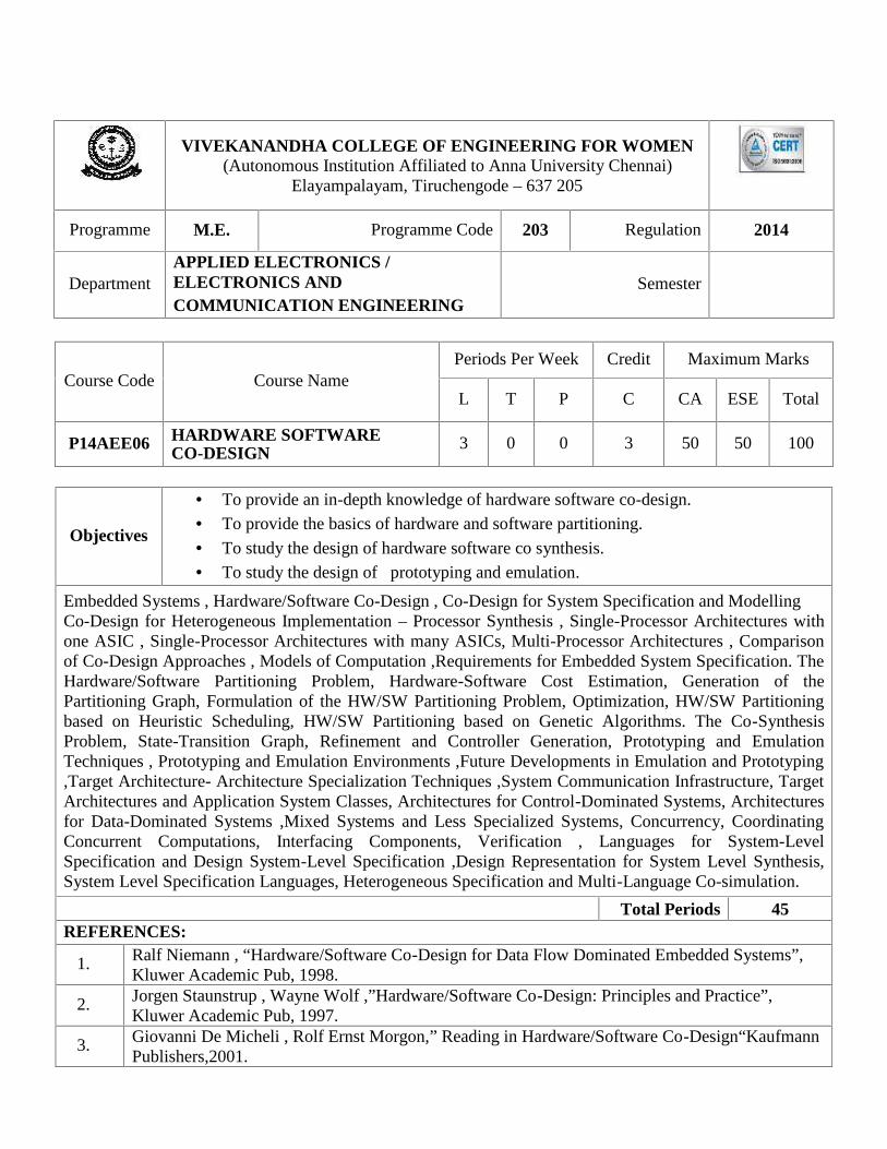
P14AEE06 HARDWARE SOFTWARECO-DESIGN
3 0 0 3 50 50 100
Objectives
To provide an in-depth knowledge of hardware software co-design. To provide the basics of hardware and software partitioning.
To study the design of hardware software co synthesis. To study the design of prototyping and emulation.
Embedded Systems , Hardware/Software Co-Design , Co-Design for System Specification and ModellingCo-Design for Heterogeneous Implementation – Processor Synthesis , Single-Processor Architectures withone ASIC , Single-Processor Architectures with many ASICs, Multi-Processor Architectures , Comparisonof Co-Design Approaches , Models of Computation ,Requirements for Embedded System Specification. TheHardware/Software Partitioning Problem, Hardware-Software Cost Estimation, Generation of thePartitioning Graph, Formulation of the HW/SW Partitioning Problem, Optimization, HW/SW Partitioningbased on Heuristic Scheduling, HW/SW Partitioning based on Genetic Algorithms. The Co-SynthesisProblem, State-Transition Graph, Refinement and Controller Generation, Prototyping and EmulationTechniques , Prototyping and Emulation Environments ,Future Developments in Emulation and Prototyping,Target Architecture- Architecture Specialization Techniques ,System Communication Infrastructure, TargetArchitectures and Application System Classes, Architectures for Control-Dominated Systems, Architecturesfor Data-Dominated Systems ,Mixed Systems and Less Specialized Systems, Concurrency, CoordinatingConcurrent Computations, Interfacing Components, Verification , Languages for System-LevelSpecification and Design System-Level Specification ,Design Representation for System Level Synthesis,System Level Specification Languages, Heterogeneous Specification and Multi-Language Co-simulation.
Total Periods 45REFERENCES:
1. Ralf Niemann , “Hardware/Software Co-Design for Data Flow Dominated Embedded Systems”,Kluwer Academic Pub, 1998.
2. Jorgen Staunstrup , Wayne Wolf ,”Hardware/Software Co-Design: Principles and Practice”,Kluwer Academic Pub, 1997.
3. Giovanni De Micheli , Rolf Ernst Morgon,” Reading in Hardware/Software Co-Design“KaufmannPublishers,2001.

VIVEKANANDHA COLLEGE OF ENGINEERING FOR WOMEN(Autonomous Institution Affiliated to Anna University Chennai)
Elayampalayam, Tiruchengode – 637 205
Programme M.E. Programme Code Regulation 2014
DepartmentVLSI DESIGN & APPLIED ELECTRONICS/ ELECTRONICS AND COMMUNICATIONENGINEERING
Semester
Course Code Course NamePeriods Per Week Credit Maximum Marks
L T P C CA ESE Total
P14VDE01PHYSICS OF NANOELECTRONIC DEVICES I
3 0 0 3 50 50 100
Objectives To study about atom, tunneling.
To study the different level Fermi-Dirac statistics. To explore modeling of scattering in semiconductors.
Particles and waves, the time-independent Schrödinger equation, states and operators, particle-in-a-box,density-of-states, harmonic oscillator, hydrogen atom, tunneling, two-level systems; Electrons in a crystallattice, quantum well, wire and dot devices, interacting quantum wells, scanning probe microscopy, excitonsin semiconductors, spin-1/2 systems and quantum bits; Identical particles fermions and bosons, fieldquantization: phonons and photons; Classical and quantum density, entropy and information, statisticalensembles, Bose-Einstein and Fermi-Dirac statistics applications to electronic devices; Non-equilibriumstatistical mechanics transition probabilities, the master equation, the Boltzmann Transport Equation forelectrons in solids; Perturbation theory, scattering rates and lifetimes in electronic devices; phononscattering in semiconductors, absorption and emission of photons in semiconductors: lasers and solar cells.
Total Periods 45REFERENCES:
1. Rainer Waser, Nano Electronics and Technology, Wiley VCH, 2003.2. Charles Poole, Introduction to Nano Technology, Wiley Interscience, 2003.
3. C.Wasshuber, Simon, Simulation of Nano Structures Computational Single-Electronics, Springer-Verlag, 2001.
4. Rainer Waser, Nano Electronics and information technology advanced electronic materials andnoveldevices, Wiley –VcH Verlag GmBh-KgaH, Germany, 2005.
5. A. Mark Reed and Takhee Lee, Molecular Nano Electronics, American Scientific Publisher,California, 2003.
6. Y.Takahashi. A Comparative Study of Single-Electron Memories, IEEE Trans. Electron Devices,1998, pp.2365–2371.

VIVEKANANDHA COLLEGE OF ENGINEERING FOR WOMEN(Autonomous Institution Affiliated to Anna University Chennai)
Elayampalayam, Tiruchengode – 637 205
Programme M.E. Programme code Regulation 2014
DepartmentVLSI DESIGN & APPLIED ELECTRONICS/ ELECTRONICS AND COMMUNICATIONENGINEERING
Semester
Course code Course NamePeriods Per Week Credit Maximum Marks
L T P C CA ESE Total
P14AEE07 ASIC DESIGN 3 0 0 3 50 50 100
Objectives To study about ASIC fundamentals. To study the different level of ASIC flow in detail.
To explore modeling of ASIC design.Introduction to ASIC, ASIC library design, Programmable ASICs, Programmable ASIC logic cells, I/O cellsand interconnects, Programmable ASIC design software, low level design entry, logic synthesis, simulation,Test, ASIC construction. System partition - FPGA partitioning - partitioning methods - floor planning -placement - physical design flow –global routing - detailed routing - special routing - circuit extraction -DRC.
Total Periods 45REFERENCES:
1. M.J.S .Smith, "Application - Specific Integrated Circuits" - Addison -Wesley Longman Inc.,1997.
2. Andrew Brown, " VLSI Circuits and Systems in Silicon", McGraw Hill, 1991
3. S.D. Brown, R.J. Francis, J. Rox, Z.G. Uranesic, " Field Programmable Gate Arrays ", KluwerAcademic Publishers, 1992.
4. Mohammed Ismail and Terri Fiez, "Analog VLSI Signal and Information Processing ", McGrawHill, 1994.
5. S. Y. Kung, H. J. Whilo House, T. Kailath, "VLSI and Modern Signal Processing ", PrenticeHall, 1985.
6. Jose E. France, Yannis Tsividis, " Design of Analog - Digital VLSI Circuits forTelecommunication and Signal Processing ", Prentice Hall, 1994.

VIVEKANANDHA COLLEGE OF ENGINEERING FOR WOMEN(Autonomous Institution Affiliated to Anna University Chennai)
Elayampalayam, Tiruchengode – 637 205
Programme M.E. Programme Code Regulation 2014
DepartmentVLSI DESIGN & APPLIED ELECTRONICS/ ELECTRONICS AND COMMUNICATIONENGINEERING
Semester
Course Code Course NamePeriods Per Week Credit Maximum Marks
L T P C CA ESE Total
P14AEE08 LOW POWER VLSI DESIGN 3 0 0 3 50 50 100
Objectives
To study the principle of low power design. To explore the concept of power optimization and estimation analysis. To understand the layout design and special techniques. To study the software design for low power techniques.
Hierarchy of limits of power – Sources of power consumption – Physics of power dissipation in CMOS FETdevices- Basic principle of low power design. Logical level power optimization – Circuit level low powerdesign – Circuit techniques for reducing power consumption in adders and multipliers– Reducing powerconsumption in memories – Low power clock, Interconnect and layout design – Advanced techniques –Special techniques Power estimation techniques – Logic level power estimation – Simulation poweranalysis– Probabilistic power analysis. Synthesis for low power –Behavioral level transforms- Softwaredesign for low power
Total Periods 45
REFERENCES:
1. K.Roy and S.C. Prasad , LOW POWER CMOS VLSI circuit design, Wiley,2000
2. Dimitrios Soudris, Chirstian Pignet, Costas Goutis, DESIGNING CMOS CIRCUITS FOR LOWPOWER, Kluwer,2002
3. J.B. Kuo and J.H Lou, Low voltage CMOS VLSI Circuits, Wiley 1999.4. A.P.Chandrakasan and R.W. Broadersen, Low power digital CMOS design, Kluwer, 1995.5. Gary Yeap, Practical low power digital VLSI design, Kluwer,1998.6. Abdellatif Bellaouar, Mohamed.I. Elmasry, “Low power digital VLSI design”, s Kluwer, 1995.
7. James B. Kuo, Shin – chia Lin, Low voltage SOI CMOS VLSI Devices and Circuits.John Wiley and sons, inc 2001
VIVEKANANDHA COLLEGE OF ENGINEERING FOR WOMEN(Autonomous Institution Affiliated to Anna University Chennai)
Elayampalayam, Tiruchengode – 637 205
Programme M.E. Programme Code Regulation 2014
DepartmentVLSI DESIGN & APPLIED ELECTRONICS/ ELECTRONICS AND COMMUNICATIONENGINEERING
Semester
Course Code Course NamePeriods Per Week Credit Maximum Marks
L T P C CA ESE Total
P14AEE09 VLSI SIGNAL PROCESSING 3 0 0 3 50 50 100
Objectives
To study the DSP Systems, Pipelining and parallel processing of FIR Filters.
To understand the concept of Retiming, Algorithmic strength reduction. To explore the Fast Convolution, Pipelining and Parallel Processing of IIR Filters. To understand Scaling, Round-Off Noise, Bit-Level Arithmetic Architectures and
Numerical Strength Reduction, Synchronous, Wave and Asynchronous Pipelining.Introduction To DSP Systems -Typical DSP algorithms; Iteration Bound – data flow graph representations,bound and iteration bound, Longest path Matrix algorithm; Pipelining and parallel processing – Pipeliningof FIR digital filters Retiming - definitions and properties; Unfolding – an algorithm for Unfolding,properties of unfolding, sample period reduction and parallel processing application; filters and transforms –2-parallel FIR filter, 2-parallel fast FIR filter, DCT algorithm architecture transformation, Fast convolutionLook-Ahead pipelining in first-order IIR filters Clustered look-ahead pipelining, Design of Lyon’s bit-serialmultipliers using Horner’s rule, bit-serial FIR filter, CSD representation, Numerical strength reduction –sub-expression elimination, multiple constant multiplication, iterative matching,
Total Periods 45REFERENCES:
1. Keshab K. Parhi, “VLSI Digital Signal Processing Systems, Design and implementation”, Wiley,Interscience, 2007.
2. U. Meyer – Baese, “Digital Signal Processing with Field Programmable Gate Arrays”, Springer,Second Edition, 2004.

VIVEKANANDHA COLLEGE OF ENGINEERING FOR WOMEN(Autonomous Institution Affiliated to Anna University Chennai)
Elayampalayam, Tiruchengode – 637 205
Programme M.E. Programme Code Regulation 2014
DepartmentVLSI DESIGN & APPLIED ELECTRONICS/ ELECTRONICS AND COMMUNICATIONENGINEERING
Semester
Course Code Course NamePeriods Per Week Credit Maximum Marks
L T P C CA ESE Total
P14VD104 CMOS ANALOG VLSI DESIGN 3 0 0 3 50 50 100
Objectives To study the Fundamentals of cascade circuits. To study the Fundamentals Basic MOS models.
Introduction to analog VLSI and mixed signal issues in CMOS technologies. Basic MOS models, SPICEModels and frequency dependent parameters. Basic MNOS/CMOS gain stage, cascade and cascade circuits.Frequency response, stability and noise issues in amplifiers. CMOS analog blocks: Current Sources andVoltage references. Differential amplifier and OPAMP design. Frequency Synthesizers and Phased lock-loop. Non-linear analog blocks: Comparators, Charge-pump circuits and Multipliers. Data converters.Analog Interconnects. Analog Testing and Layout issues. Low Voltage and Low Power Circuits.Introduction to RF Electronics. Basic concepts in RF design.
Total Periods 45REFERENCES:
1. R.JacobBaker, H.W.Li, and D.E. Boyce CMOS Circuit Design ,Layout and Simulation, Prentice-Hall of , 1998
2. Mohammed Ismail and Terri Faiz Analog VLSI Signal and Information Process, McGraw-Hill Bookcompany, 1994
3. Paul R. Gray and R.G.Meyer, Analysis and design of Analog Integrated circuits John Wiley andsons,,(3rd Edition), 1993
4. B. Razavi, RF Microelectronics, Prentice-Hall PTR, 1998
5. Journals: 1) IEEE Journal of Solid state Circuits2) IEEE Trans. on Communications

VIVEKANANDHA COLLEGE OF ENGINEERING FOR WOMEN(Autonomous Institution Affiliated to Anna University Chennai)
Elayampalayam, Tiruchengode – 637 205
Programme M.E. Programme Code Regulation 2014
DepartmentVLSI DESIGN & APPLIED ELECTRONICS/ ELECTRONICS AND COMMUNICATIONENGINEERING
Semester
Course Code Course NamePeriods Per Week Credit Maximum Marks
L T P C CA ESE Total
P14VD210 FOUNDATIONS OF VLSI CAD 3 0 0 3 50 50 100
Objectives To study about complementary orthogonality.
To study the different level linear equations and Graphs. To explore modeling of Data structures such as stacks.
Matrices: Linear dependence of vectors, solution of linear equations, bases of vector spaces, orthogonality,complementary orthogonal spaces and solution spaces of linear equations; Graphs: representation of graphsusing matrices; Paths, connectedness; circuits, cutsets, trees; Fundamental circuit and cutset matrices;Voltage and current spaces of a directed graph and their complementary orthogonality; Algorithms and datastructures: efficient representation of graphs; Elementary graph algorithms involving BFS and DFS trees,such as finding connected and 2- connected components of a graph, the minimum spanning tree, shortestpath between a pair of vertices in a graph; Data structures such as stacks, linked lists and queues, binarytrees and heaps. Time and space complexity of algorithms.
Total Periods 45REFERENCES:
1. K. Hoffman and R.E. Kunze, Linear Algebra, Prentice Hall (India), 19862. T.Cormen, C.Leiserson and R.A.Rivest, Algorithms, MIT Press and McGraw-Hill, 1990

VIVEKANANDHA COLLEGE OF ENGINEERING FOR WOMEN(Autonomous Institution Affiliated to Anna University Chennai)
Elayampalayam, Tiruchengode – 637 205
Programme M.E. Programme Code 203 Regulation 2014
DepartmentAPPLIED ELECTRONICS /ELECTRONICS AND
COMMUNICATION ENGINEERINGSemester
Course Code Course NamePeriods Per Week Credit Maximum Marks
L T P C CA ESE Total
P14VDE01HIGH PERFORMANCECOMPUTER NETWORKS
3 0 0 3 50 50 100
Objectives
To develop a comprehensive understanding of network architectures, protocols,control and performances
To focus on the convergence of computer networking, and wireless networks thatexplains current and emerging networking technologies.
Multimedia Networking Applications, VPN-Remote-Access VPN, site-to-site VPN, Tunneling to PPP,Security in VPN. MPLS operation, Routing, Tunneling and use of FEC, Traffic Engineering, and MPLSbased VPN, overlay networks - P2P connections. Traffic Modeling, Little’s theorem, Need for modeling,Poisson modeling and its failure, Non- Poisson models, Network performance evaluation. Principles ofcryptography – Authentication – integrity – key distribution and certification. Access control and fire wallsattacks and counter measures - security in many layers. Infrastructure for network management– Theinternet standard management framework – SMI, MIB, SNMP, Security and administration – ASN.1.
Total Periods 45REFERENCES:
1.Walrand .J. Varatya, High performance communication network, Margan Kanffman – HarcourtAsia Pvt. Ltd. 2nd Edition, 2000.
2.J.F. Kurose & K.W. Ross,”Computer Networking- A top down approach featuring the internet”,Pearson, 2nd Edition, 2003.
3. Nader F.Mir, Computer and Communication Networks, first edition.FURTHER READINGS:
1.Aunuragkumar, D. Manjunath, Joy kuri, “Communication Networking”, Morgan KaufmannPublishers, 1ed 2004.
2. Larry l.Peterson & BruceS.David, “Computer Networks: A System Approach”-1996


![Vivekanandha College of Engineering for Women - Tiruchengode PROJECT REPORT-UG re.doc · Web viewVIVEKANANDHA COLLEGE OF ENGINEERING FOR WOMEN [Autonomous] Approved by AICTE, New](https://static.fdocuments.us/doc/165x107/613732a20ad5d206764876eb/vivekanandha-college-of-engineering-for-women-tiruchengode-project-report-ug-redoc.jpg)