EL9800 Base Board - Beckhoff Electrically Erasable Programmable Read Only Memory. ... Introduction...
32
EL9800 Base Board Version: 4.0.1 Date: 2016-08-25
Transcript of EL9800 Base Board - Beckhoff Electrically Erasable Programmable Read Only Memory. ... Introduction...

EL9800 Base Board Version: 4.0.1 Date: 2016-08-25


Content
EL9800 1
Content
1 Legal Notice 5
1.1 Trademarks 5
1.2 Patent Pending 5
1.3 Disclaimer 5
1.4 Copyright 5
1.5 Safety Instructions 6
1.5.1 Delivery Status 6
1.5.2 Description of safety symbols 6
1.6 Documentation issue status 7
2 Product overview 8
2.1 Power Supply 9
2.2 Process Data Interface for EtherCAT postage stamps 10
2.2.1 Process data interface dependent pinout of the headers J202 and TP202 11
2.3 PDI-Selection 12
2.4 8/16 Bit µC-PDI-Interface 14
2.5 32 Bit Digital-PDI-Interface 16
2.6 PIC PDI-Interface 18
2.7 SPI-PDI-Interface 21
2.8 Distributed Clocks 21
2.9 FPGA-Programmer 22
2.10 PIC-Programmer 23
3 Altera Quartus II Programmer™ 25
3.1 Selecting the programming hardware 26
3.2 Conversion of a SOF-File in the JIC-file format 27
3.3 Choosing the programming file 29
3.4 Programming of the FPGA/EEPROM 29
4 Appendix 30
4.1 Support and Service 30
4.1.1 Beckhoff's branch offices and representatives 30
4.2 Beckhoff Headquarters 30

Content
2 EL9800
TABLES
Table 1 Pinout of the headers J202 and TP202 ......................................................................................... 11 Table 2 Positions of the PDI-Selector ......................................................................................................... 12 Table 3 Pinout of the connectors TP208 and J208 .................................................................................... 14 Table 4 Pinout of the connector TP206 ...................................................................................................... 15 Table 5 Port configuration of the digital PDI ............................................................................................... 16 Table 6 Definition of the OE_CONF and OE_EXT signals ......................................................................... 16 Table 7 Pinout of the connectors TP207 and J207 .................................................................................... 17 Table 8 Pinout of the connector J900 ......................................................................................................... 18 Table 9 Location of the inputs and output ports on the PIC- ...................................................................... 19 Table 10 Connection of SPI-interface, EEPROM and programming interface with the PIC24H ............... 19 Table 11 Pinout of the connectors TP209 and J209 .................................................................................. 19 Table 12 Pinout of the connector J510 ....................................................................................................... 20 Table 13 Pinout of the connector J1005 ..................................................................................................... 20 Table 14 Pinout of the connectors TP204 and J204 .................................................................................. 21

Content
EL9800 3
FIGURES
Figure 1 Overview about the EL9800 ............................................................................................................8 Figure 2 Power Supply ..................................................................................................................................9 Figure 3 Pinout of the header J1203 .............................................................................................................9 Figure 4 Header J1200 – Selection of the PDI header voltage .....................................................................9 Figure 5 Connection area fort he EtherCAT postage stamp ...................................................................... 10 Figure 6 Pinout of the connectors J202 and TP202 ................................................................................... 10 Figure 7 PDI-Selection Area ....................................................................................................................... 12 Figure 8 Pinout of the connector J1201 ..................................................................................................... 13 Figure 9 µ-Controller PDI-Interface ............................................................................................................ 14 Figure 10 Power pins on the connectors TP208 and J208 ........................................................................ 14 Figure 11 Digital IO PDI-Interface .............................................................................................................. 16 Figure 12 Voltages on the headers TP207 und J207 ................................................................................. 18 Figure 13 PIC PDI-Interface ....................................................................................................................... 18 Figure 14 Configuration and Status-Area of the Distributed Clocks .......................................................... 21 Figure 15 FPGA Programming Interface .................................................................................................... 22 Figure 16 PIC Programming Interface ........................................................................................................ 23 Figure 17 Quartus II Programmer™ ........................................................................................................... 25 Figure 18 Hardware Setup Dialog .............................................................................................................. 26 Figure 19 Setup Dialog – USB Blaster selected......................................................................................... 26 Figure 20 Quartus II Programmer Dialog after „Auto-Detect“ processing .................................................. 27 Figure 21 Convert Programming Files ....................................................................................................... 28 Figure 22 Selection of the programming file ............................................................................................... 29
Content
4 EL9800
ABBREVIATIONS
DC Direct Current
EEPROM Electrically Erasable Programmable Read Only Memory. Non-volatile memory used
to store ESC configuration and description.
ESC EtherCAT Slave Controller
EtherCAT Real-time Standard for Industrial Ethernet Control Automation Technology
GND-Earth Ground-Earth
LED Light Emitting Diode, used as an indicator
PCB Printed Circuit Board
PDI Process Data interface
SPI Serial Peripheral Interface
RJ45 FCC Registered Jack, standard Ethernet connector (8P8C)

Legal Notice
EL9800 5
1 Legal Notice
1.1 Trademarks
Beckhoff®, TwinCAT®, EtherCAT®, Safety over EtherCAT®, TwinSAFE® and XFC® are registered trade-
marks of and licensed by Beckhoff Automation GmbH. Other designations used in this publication may be
trademarks whose use by third parties for their own purposes could violate the rights of the owners.
1.2 Patent Pending
The EtherCAT Technology is covered, including but not limited to the following German patent applica-
tions and patents: DE10304637, DE102004044764, DE102005009224, DE102007017835 with corre-
sponding applications or registrations in various other countries.
1.3 Disclaimer
The documentation has been prepared with care. The products described are, however, constantly under
development. For that reason the documentation is not in every case checked for consistency with per-
formance data, standards or other characteristics. In the event that it contains technical or editorial errors,
we retain the right to make alterations at any time and without warning. No claims for the modification of
products that have already been supplied may be made on the basis of the data, diagrams and descrip-
tions in this documentation.
1.4 Copyright
© Beckhoff Automation GmbH 05/2009.
The reproduction, distribution and utilization of this document as well as the communication of its contents
to others without express authorization are prohibited. Offenders will be held liable for the payment of
damages. All rights reserved in the event of the grant of a patent, utility model or design.

Legal Notice
6 EL9800
1.5 Safety Instructions
Consider the following safety instructions and descriptions!
Product specific safety instructions are to be found on the following pages or in the areas mounting, wir-
ing, commissioning etc.
1.5.1 Delivery Status
All the components are supplied in particular hardware and software configurations appropriate for the application. Modifications to hardware or software configurations other than those described in the docu-mentation are not permitted, and nullify the liability of Beckhoff Automation GmbH. Product specific safety instructions are to be found on the following pages or in the areas mounting, wiring, commissioning etc.
1.5.2 Description of safety symbols
The following safety symbols are used in this documentation. They are intended to alert the reader to the
associated safety instructions.
DANGER
Acute risk of injury!
If you do not adhere the safety advise adjoining this symbol, there is immediate danger to life and health of individuals!
WARNING
Risk of injury!
If you do not adhere the safety advise adjoining this symbol, there is danger to life and health of individuals!
CAUTION
Hazard to individuals, environment and devices!
If you do not adhere the safety advise adjoining this symbol, there is obvious hazard to individuals, environment and materials!
Note
Note or pointer
This symbol indicates information that contributes to better understanding.

Legal Notice
EL9800 7
1.6 Documentation issue status
Version Comment
4.0.0 First version – Introduction of the EL9800.6A version
PIC programmer changed from “ICD2” to “PICkit OnBoard”
4.0.1 Pin 1 marking changed for connector J1005
Product overview
8 EL9800
2 Product overview
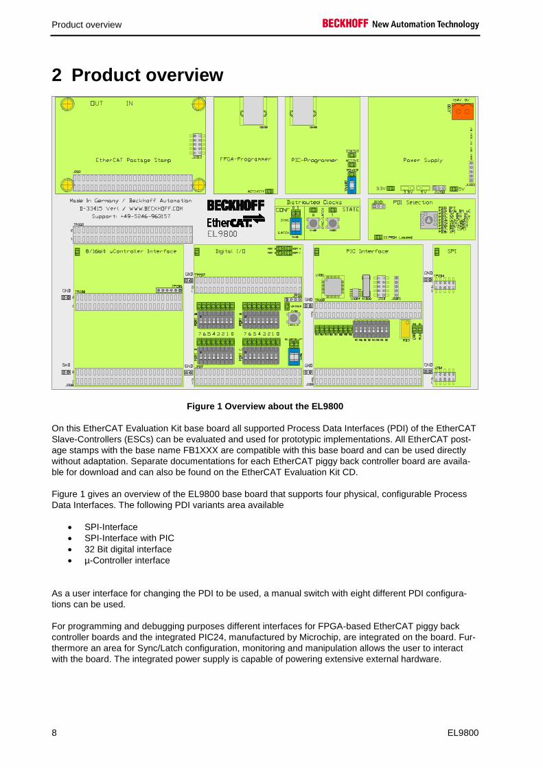
Figure 1 Overview about the EL9800
On this EtherCAT Evaluation Kit base board all supported Process Data Interfaces (PDI) of the EtherCAT
Slave-Controllers (ESCs) can be evaluated and used for prototypic implementations. All EtherCAT post-
age stamps with the base name FB1XXX are compatible with this base board and can be used directly
without adaptation. Separate documentations for each EtherCAT piggy back controller board are availa-
ble for download and can also be found on the EtherCAT Evaluation Kit CD.
Figure 1 gives an overview of the EL9800 base board that supports four physical, configurable Process
Data Interfaces. The following PDI variants area available
SPI-Interface
SPI-Interface with PIC
32 Bit digital interface
µ-Controller interface
As a user interface for changing the PDI to be used, a manual switch with eight different PDI configura-
tions can be used.
For programming and debugging purposes different interfaces for FPGA-based EtherCAT piggy back
controller boards and the integrated PIC24, manufactured by Microchip, are integrated on the board. Fur-
thermore an area for Sync/Latch configuration, monitoring and manipulation allows the user to interact
with the board. The integrated power supply is capable of powering extensive external hardware.
Product overview
EL9800 9
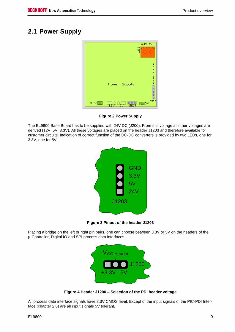
2.1 Power Supply
Figure 2 Power Supply
The EL9800 Base Board has to be supplied with 24V DC (J200). From this voltage all other voltages are
derived (12V, 5V, 3.3V). All these voltages are placed on the header J1203 and therefore available for
customer circuits. Indication of correct function of the DC-DC converters is provided by two LEDs, one for
3.3V, one for 5V.
J1203
24V
5V
3.3V
GND
Figure 3 Pinout of the header J1203
Placing a bridge on the left or right pin pairs, one can choose between 3.3V or 5V on the headers of the
µ-Controller, Digital IO and SPI process data interfaces.
+3.3V 5V
VCC Header
J1200
Figure 4 Header J1200 – Selection of the PDI header voltage
All process data interface signals have 3.3V CMOS level. Except of the input signals of the PIC-PDI Inter-
face (chapter 2.6) are all input signals 5V tolerant.

Product overview
10 EL9800
2.2 Process Data Interface for EtherCAT postage stamps
Figure 5 Connection area fort he EtherCAT postage stamp
Within this area all EtherCAT postage stamps are attached to the base board. Communication between
EtherCAT postage stamp and the EL9800 base boards takes place over the connector J202. In case of
FPGA-based EtherCAT Slave Controller boards configuration and debugging of the FPGA is done using
the connector J203. The headers J202 and TP202 pinouts are identical. Therefore all process data sig-
nals of any EtherCAT postage stamp can be measures without delay or be used for external customer
circuitry. The signal definition on the two connectors, despite of the power supply pins, may differ from
EtherCat postage stamp to EhterCAT postage stamp.
2
9
20
27
38
45
48 50
49
VCC (5V)
+3.3V
GND
1 Pin Number
56
551
Figure 6 Pinout of the connectors J202 and TP202
Figure 6 shows the pinout of the connectors J202 and TP202 with power in- and outputs signals. Each
EtherCAT postage Stamp supplies its own IO-voltage of 3.3V on the pin 49 on the connectors J202 and
TP202.
Maximal transfer rates between an EtherCAT postage stamp and external circuitry can be achieved when
interfacing with the connector TP202. In this case direct communication between both devices is estab-
lished, bypassing the PDIs bus drivers.
Product overview
EL9800 11
2.2.1 Process data interface dependent pinout of the headers J202 and TP202
The pinout of the headers J202 and TP202 are depending on the choice of the process data interface on
the EL9800 base board. In Table 1 the pinout of these headers are listed for the process interfaces Digital
IO, SPI and the different Microcontroller interfaces.
Table 1 Pinout of the headers J202 and TP202
Pin number Digital IO SPI 8/16bit sync./as. µC
1 I/O[0] GPI[6] A[0]
2 GND
3 I/O[2] GPI[4] A[2]
4 I/O[1] GPI[5] A[1]
5 I/O[4] GPO[6] A[4]
6 I/O[3] GPO[7] A[3]
7 I/O[6] GPO[4] A[6]
8 I/O[5] GPO[5] A[5]
9 GND
10 I/O[7] GPI[3] A[7]
11 I/O[9] GPI[1] A[9]
12 I/O[8] GPI[2] A[8]
13 I/O[11] GPO[3] A[11]
14 I/O[10] GPI[0] A[10]
15 I/O[13] EEPROM Loaded
16 I/O[12] GPO[2] A[12]
17 I/O[15] GPI[11] CPU_CLK_IN
18 I/O[14] GPO[1] A[13]
19 I/O[16] GPI[7] D[0]
20 GND
21 I/O[18] SPI_SEL D[2]
22 I/O[17] GPO[8] D[1]
23 I/O[20] GPO[11] D[4]
24 I/O[19] GPO[10] D[3]
25 I/O[22] SPI_INT D[6]
26 I/O[21] GPI[8] D[5]
27 GND
28 I/O[23] GPI[10] D[7]
29 I/O[25] GPO[13] D[8]
30 I/O[24] SPI_D_IN D[8]
31 I/O[27] GPO[15] D[11]
32 I/O[26] SPI_D_OUT D[10]
33 I/O[29] GPI[13] D[13]
34 I/O[28] GPI[12] D[12]
35 I/O[31] GPI[15] D[15]
36 I/O[30] GPI[14] D[14]
37 WD_TRIGGER SPI_CLK nCS
38 GND
39 SOF N.C. RDnWR/nWR
40 OUT_VALID N.C. nTS/nRD
41 SYNC[0]/LATCH[0]
Product overview
12 EL9800
Pin number Digital IO SPI 8/16bit sync./as. µC
42 N.C. N.C. nBHE
43 LATCH_IN N.C. IRQ
44 SYNC[1]/LATCH[1]
45 GND
46 OE N.C. nTA/nBUSY
47 N.C.
48 VCC
49 3.3V Out
50 VCC (5V Input)
51 CLK25_OUT N.C. A[15]
52 OE_CONF GPO[0] A[14]
53 Not Used
54 Not Used
55 Not Used
56 Not Used
Note
Usage of the FB1111-0142 with differing PDIs
The usage of the FB1111-0142 with the PDIs SPI and µ-Controller is only supported
for evaluation purposes in combination with the EL9800 base board. Therefore the
pinout of the headers J202 and TP202 is not supported in these cases.
In custom devices the usage of postage stamps with the appropriate PDI is recom-
mended.
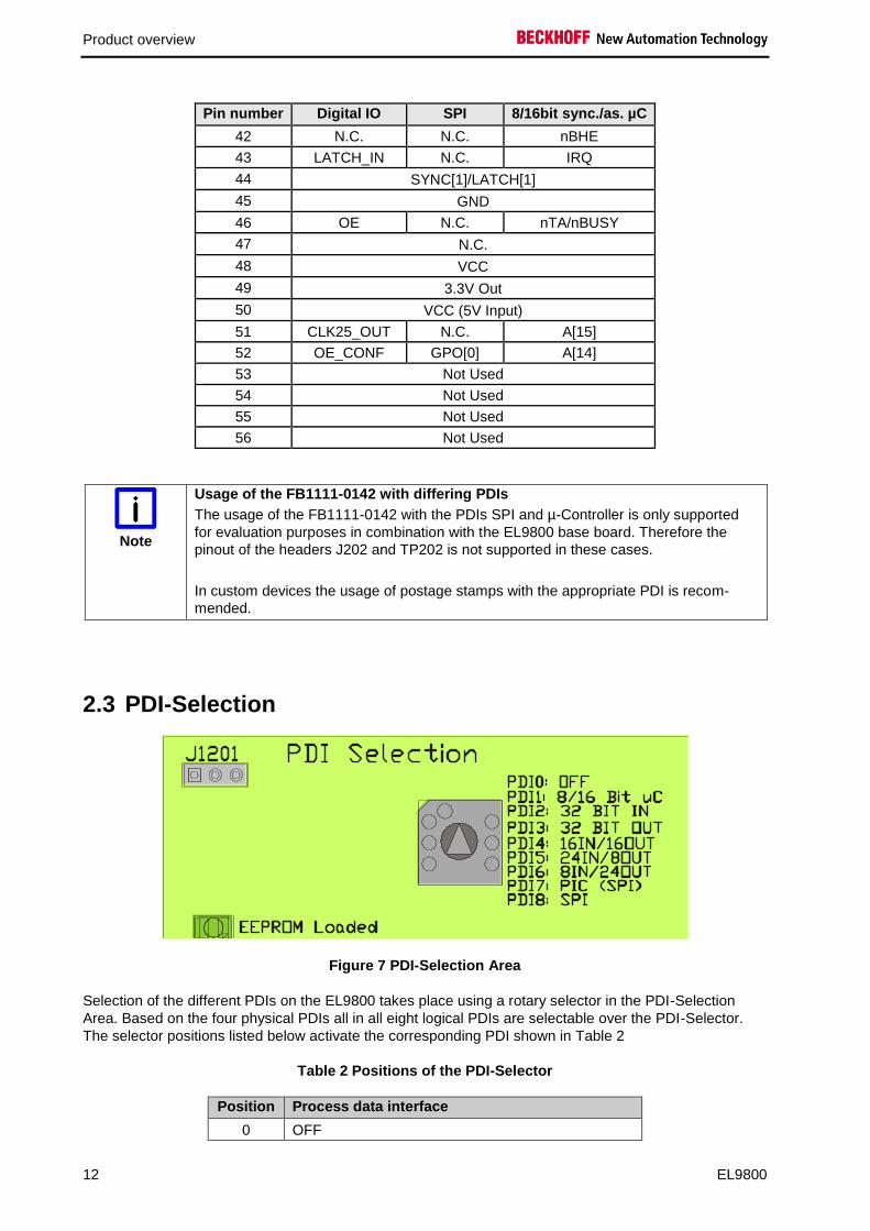
2.3 PDI-Selection
Figure 7 PDI-Selection Area
Selection of the different PDIs on the EL9800 takes place using a rotary selector in the PDI-Selection
Area. Based on the four physical PDIs all in all eight logical PDIs are selectable over the PDI-Selector.
The selector positions listed below activate the corresponding PDI shown in Table 2
Table 2 Positions of the PDI-Selector
Position Process data interface
0 OFF

Product overview
EL9800 13
1 8/16 Bit µ-Controller Interface
2 32 Bit digital Interface - 32 Inputs
3 32 Bit digital Interface - 32 Outputs
4 32 Bit digital Interface - 16 Inputs / 16 Outputs
5 32 Bit digital Interface - 24 Inputs / 8 Outputs
6 32 Bit digital Interface - 8 Inputs / 24 Outputs
7 PIC (SPI)
8 SPI
All postage stamps indicate successful loading of the EtherCAT configuration from the EEPROM with an
LED in the EL9800 base board.
The EL9800 base board supports automatic differentiation between FPGA-based postage stamps and
ASIC (e.g. ET1100) based ones. Therefore the programming voltage on the connector J203 is detected
and evaluated. In case of a missing programming voltage the behaviour of the EL9800 base board can be
configured using the connector J1202. Figure 8 shows the pinout of the connector J1202.
+3.3V GND
FB-Detect
Figure 8 Pinout of the connector J1201
The delivery status of this connector is not bridged. FB-Detect has to be bridged to +3.3V, when FB1111-
140 and FB1111-141 postage stamps are used in combination with the EL9800 evaluation board. Pre-
condition for correct communication between EtherCAT postage stamp and EL9800 base board is the
correct configuration of the EtherCAT device. As well on the IP-Core based FPGA postage stamps as on
ET1100-ASIC based postage stamps the process data interface has to be configured by loading the spe-
cific binary file into the configuration EEPROM (*bin).

Product overview
14 EL9800
2.4 8/16 Bit µC-PDI-Interface
Figure 9 µ-Controller PDI-Interface
Within this area customer specific µ-Controller hardware can be attached as well as the communication
between EtherCAT-Slave-Controller and µ-Controller can be monitored. µ-Controller with 8 and 16 bit
data with are supported by the EL9800 base board. An address space of 16 Bit is available on the con-
nectors J208/TP208 and TP206. The logical levels are implemented in accordance with the Intel configu-
ration (C166, SH1, etc.)
2
VCC
GND
1 Pin Number
50
491
Figure 10 Power pins on the connectors TP208 and J208
Both of the connectors TP208 and J208 (Figure 10) have an identical signal and power pinout. While
connector TP208 is assigned to measuring purposes, the connector J208 is designated for interfacing
external hardware.Table 3 lists the pinout of the connectors TP208 and J208.
Table 3 Pinout of the connectors TP208 and J208
Pin Signal Pin Signal
1 GND 2 Vcc

Product overview
EL9800 15
3 A0 4 A1
5 A2 6 A3
7 A4 8 A5
9 A6 10 A7
11 GND 12 Vcc
13 A8 14 A9
15 A10 16 A11
17 A12 18 A13
19 GND 20 Vcc
21 D0 22 D1
23 D2 24 D3
25 D4 26 D5
27 D6 28 D7
29 GND 30 Vcc
31 D8 32 D9
33 D10 34 D11
35 D12 36 D13
37 D14 38 D15
39 GND 40 Vcc
41 nCS 42 nRD (nTS)
43 nWR 44 nBHE
45 nBUSY (nTA) 46 nINT
47 Port E4 (SYNC0) 48 Port E5 (SYNC1)
49 GND 50 Vcc
Additional signals like the upper address lines of the µ-Controfller interface are lead through the connect-
or TP206. The pinout of this connector is shown in Table 4.
Table 4 Pinout of the connector TP206
Pin Signal
1 VCC
2 A14
3 A15
4 CPU_CLK_IN
5 EEPROM_Loaded
6 GND

Product overview
16 EL9800
2.5 32 Bit Digital-PDI-Interface
Figure 11 Digital IO PDI-Interface
Additional to the input and output signals the digital process data interface contains configuration and
status signals. Using the PDI-Selector byte wise configuration of the 32 digital signals is supported. The
following combinations are selectable (Table 5).
Table 5 Port configuration of the digital PDI
Position Process Data Interface Port A Port B Port C Port D
2 32 Bit digital Interface - 32 Inputs IN IN IN IN
3 32 Bit digital Interface - 32 Outputs OUT OUT OUT OUT
4 32 Bit digital Interface - 16 Inputs / 16 Outputs IN IN OUT OUT
5 32 Bit digital Interface - 24 Inputs / 8 Outputs IN IN IN OUT
6 32 Bit digital Interface - 8 Inputs / 24 Outputs IN OUT OUT OUT
Four LEDs in the top right edge of the digital PDI area are showing the configuration of the data bytes.
The LEDs are active, if the corresponding Byte (Port A to Port D) is configured as an output from the
EtherCAT postage stamps view. Furthermore eight LEDs and Switches are assigned to each port, for
input and output purposes respectively.
The lower right section of the digital PDI interface is assigned to configuration and status indication of the
digital PDI. The Switch SW904 configures the signals OE_CONG and OE_EXT according to Table 6.
Table 6 Definition of the OE_CONF and OE_EXT signals
Signal Function Polarity
OE_CONF Output Configuration – Behavior of the output signals in case of a falling edge of the WD_STATE signal. Or when OE_EXT is low re-spectively
Positive
OE_EXT Output Enable – Enables the output of the output signals. Positive
Manual latching in of the input data can be controlled by activating the switch SW905. Furthermore the
state of the EtherCAT-Slave-Controllers (ESC) watchdog is indicated by the “WD-State” LED is active. In

Product overview
EL9800 17
opposite the LED is inactive, if the watchdog has fallen off. Again the connectors TP207 (Measuring) and
J207 (external hardware) have an identical pinout, as shown in Table 7.
Table 7 Pinout of the connectors TP207 and J207
Pin Signal Pin Signal
1 I/O 0 2 I/O 1
3 I/O 2 4 I/O 3
5 I/O 4 6 I/O 5
7 I/O 6 8 I/O 7
9 GND 10 Vcc
11 I/O 8 12 I/O 9
13 I/O 10 14 I/O 11
15 I/O 12 16 I/O 13
17 I/O 14 18 I/O 15
19 GND 20 Vcc
21 I/O 16 22 I/O 17
23 I/O 18 24 I/O 19
25 I/O 20 26 I/O 21
27 I/O 22 28 I/O 23
29 GND 30 Vcc
31 I/O 24 32 I/O 25
33 I/O 26 34 I/O 27
35 I/O 28 36 I/O 29
37 I/O 30 38 I/O 31
39 GND 40 Vcc
41 IN Valid 42 OUT valid
43 Port E2 44 Port E3
45 Port E4 (SYNC0) 46 Port E5 (SYNC1)
47 Port E6 48 Port E7
49 GND 50 Vcc
Product overview
18 EL9800
Additional signals are available on the connector J900 (Table 8).
Table 8 Pinout of the connector J900
Pin Signal
1 VCC
2 WD_STATE
3 OE_CONF
4 GND
2
VCC
GND
1 Pin Number
50
491
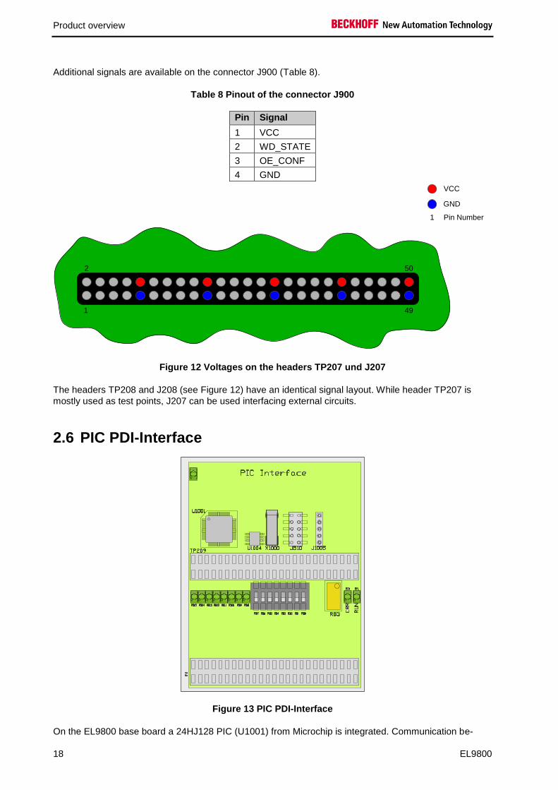
Figure 12 Voltages on the headers TP207 und J207
The headers TP208 and J208 (see Figure 12) have an identical signal layout. While header TP207 is
mostly used as test points, J207 can be used interfacing external circuits.
2.6 PIC PDI-Interface
Figure 13 PIC PDI-Interface
On the EL9800 base board a 24HJ128 PIC (U1001) from Microchip is integrated. Communication be-
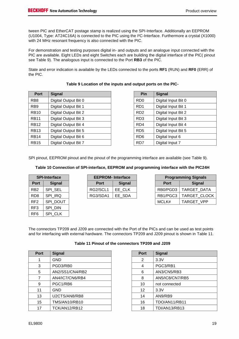
Product overview
EL9800 19
tween PIC and EtherCAT postage stamp is realized using the SPI-Interface. Additionally an EEPROM
(U1004, Type: AT24C16A) is connected to the PIC using the I²C-Interface. Furthermore a crystal (X1000)
with 24 MHz resonant frequency is also connected with the PIC.
For demonstration and testing purposes digital in- and outputs and an analogue input connected with the
PIC are available. Eight LEDs and eight Switches each are building the digital interface of the PIC( pinout
see Table 9). The analogous input is connected to the Port RB3 of the PIC.
State and error indication is available by the LEDs connected to the ports RF1 (RUN) and RF0 (ERR) of
the PIC.
Table 9 Location of the inputs and output ports on the PIC-
Port Signal Pin Signal
RB8 Digital Output Bit 0 RD0 Digital Input Bit 0
RB9 Digital Output Bit 1 RD1 Digital Input Bit 1
RB10 Digital Output Bit 2 RD2 Digital Input Bit 2
RB11 Digital Output Bit 3 RD3 Digital Input Bit 3
RB12 Digital Output Bit 4 RD4 Digital Input Bit 4
RB13 Digital Output Bit 5 RD5 Digital Input Bit 5
RB14 Digital Output Bit 6 RD6 Digital Input 6
RB15 Digital Output Bit 7 RD7 Digital Input 7
SPI pinout, EEPROM pinout and the pinout of the programming interface are available (see Table 9).
Table 10 Connection of SPI-interface, EEPROM and programming interface with the PIC24H
SPI-Interface EEPROM- Interface Programming Signals
Port Signal Port Signal Port Signal
RB2 SPI_SEL RG2/SCL1 EE_CLK RB0/PGD3 TARGET_DATA
RD8 SPI_IRQ RG3/SDA1 EE_SDA RB1/PGC3 TARGET_CLOCK
RF2 SPI_DOUT MCLK# TARGET_VPP
RF3 SPI_DIN
RF6 SPI_CLK
The connectors TP209 and J209 are connected with the Port of the PICs and can be used as test points
and for interfacing with external hardware. The connectors TP209 and J209 pinout is shown in Table 11.
Table 11 Pinout of the connectors TP209 and J209
Port Signal Port Signal
1 GND 2 3.3V
3 PGD3/RB0 4 PGC3/RB1
5 AN2/SS1/CN4/RB2 6 AN3/CN5/RB3
7 AN4/IC7/CN6/RB4 8 AN5/IC8/CN7/RB5
9 PGC1/RB6 10 not connected
11 GND 12 3.3V
13 U2CTS/AN8/RB8 14 AN9/RB9
15 TMS/AN10/RB10 16 TDO/AN11/RB11
17 TCK/AN12/RB12 18 TDI/AN13/RB13
Product overview
20 EL9800
19 U2RTS/AN14/RB14 20 AN15/OCFB/CN12/RB15
21 GND 22 3.3V
23 SCK2/CN8/RG6 24 SDI2/CN9/RG7
25 SDO2/CN10/RG8 26 SS2/T5CK/CN11/RG9
27 RG12 28 RG13
29 RG14 30 RG15
31 GND 32 3.3V
33 RF0 34 RF1
35 U1RX/SDI1/RF2 36 U1TX/SDO1/RF3
37 U2RX/SDA2/CN17/RF4 38 U2TX/SCL2/CN18/RF5
39 GND 40 3.3V
41 U1RTS/SCK1/INT0/RF6 42 IC1/INT1/RD8
43 EEPROM_Loaded 44 AN17/T3CK/T6CK/RC2
45 PGD2//RC13 46. PGC2//RC14
47 GND 48 3.3V
49 IC3/INT3/RD10(SYNC0) 50 IC4/INT4/RD11 (SYNC1)
The SPI-signals together with the Sync-Signals and the EEPROM_Loaded signal are additionally fed out
on the connector J510. The pinout of this header is listed in Table 12.
Table 12 Pinout of the connector J510
Pin Signal Pin Signal
1 SPI_CLK_IN 2 3.3V
3 EEPROM_LOADED 4 SYNC0/LATCH0
5 SPI_DIN 6 SPI_SEL
7 SPI_DOUT 8 SYNC1/LATCH1
9 SPI_INTERRUPT 10 GND
Table 13 Pinout of the connector J1005
Pin Signal
1 3.3V
2 RC14/PGC2
3 RC13/PGD2
4 MCLR#
5 GND
Product overview
EL9800 21
2.7 SPI-PDI-Interface
Similar to the µ-Controller interface this interface only consists of two connectors (TP204 and J204),
which can as well be used as test points as for connection with external hardware. Again the pinout of
both connectors is identical and therefore listed in Table 14.
Table 14 Pinout of the connectors TP204 and J204
Pin Signal Pin Signal
1 SPI_CLK_IN 2 3.3V
3 EEPROM_LOADED 4 SYNC0/LATCH0
5 SPI_DIN 6 SPI_SEL
7 SPI_DOUT 8 SYNC1/LATCH1
9 SPI_INTERRUPT 10 GND
The maximum achievable data transfer rates using this interface are depending mainly from the Ether-
CAT-Slave-Controller used in combination with the EL9800 base board. Data transfer rates are also de-
pending on the bus driver (SN74LVC245A from Texas Instruments) used on the base board. Details in-
formation about these rates can be found in both devices datasheets.
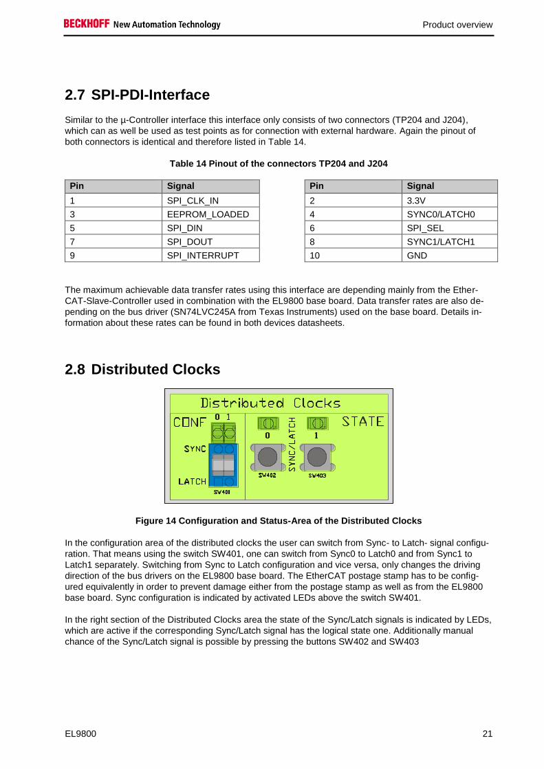
2.8 Distributed Clocks
Figure 14 Configuration and Status-Area of the Distributed Clocks
In the configuration area of the distributed clocks the user can switch from Sync- to Latch- signal configu-
ration. That means using the switch SW401, one can switch from Sync0 to Latch0 and from Sync1 to
Latch1 separately. Switching from Sync to Latch configuration and vice versa, only changes the driving
direction of the bus drivers on the EL9800 base board. The EtherCAT postage stamp has to be config-
ured equivalently in order to prevent damage either from the postage stamp as well as from the EL9800
base board. Sync configuration is indicated by activated LEDs above the switch SW401.
In the right section of the Distributed Clocks area the state of the Sync/Latch signals is indicated by LEDs,
which are active if the corresponding Sync/Latch signal has the logical state one. Additionally manual
chance of the Sync/Latch signal is possible by pressing the buttons SW402 and SW403

Product overview
22 EL9800
2.9 FPGA-Programmer
Figure 15 FPGA Programming Interface
If FPGA-based EtherCAT postage stamps are used in combination with the EL9800 base board, these
postage stamps can be programmed and debugged using the integrated FPGA programming hardware
on the EL9800. The FPGA-Programmers USB-Port has to be connected with the PC using the USB ca-
ble, which is provided with this Evaluation Kit. A FPGA based EtherCAT postage stamp can as well be
programmed using the TwinCAT Systemmanager as well as the Altera Quartus II Programmer. The pro-
gramming hardware on the EL9800 evaluation board supports programming of Altera FPGAs only (e.g.
FB1122).
Programming activity is indicated by the “ACTIVITY” LED on the board.
Detailed information about the programming operation using the Altera Quartus programmer is given in
chapter 3.

Product overview
EL9800 23
2.10 PIC-Programmer
Figure 16 PIC Programming Interface
The PIC24H integrated on the EL9800 base board can be programmed using this interface. If its USB-
port is connected with the PC using the USB-cable delivered with this Evaluation Kit, the PIC can be pro-
grammed with the development software “MPLAB” from Microchip.
If power is supplied to the EL9800 base board then the PIC programming interface can be activated by
turning on the switch SW600. Different LEDs are showing the programming state during programming
operation. The “POWER”-LED is switched on, when SW600 is in position “ON”. The “ACTIVE”-LED is
flashing during the programming process. When the target device is programmes successfully, then the
“STATUS”-LED flashes green. If it fails, the LED turns red.
A freeware version of the development environment MPLAB can be found on the Evaluation Kit CD.
CAUTION
Possible malfunction of the PIC Programming Interface
At the beginning of the programming sequence an operating system may be down-loaded onto the programming interface. During the download operation neither power may be cycled nor may the position of the switch SW600 be altered.
Not obeying this warning leads to an incomplete download of the operating system that will cause the permanent malfunction of the programming interface.
In order to achieve a successful programming of the PIC the steps listed below should be followed:
1. Turn on the power supply
2. Switch on the programming interface. Switch SW800 in „ON“-Position.
3. Connect the programming interface of the EL9800 with the PC, using the USB-Cable, delivered
together with this Evaluation KIT.
4. Start development environment MPLAB from Micochip

Product overview
24 EL9800
5. Select programming device
a. MPLAB 8: In the menu choose “Programmer => Select Programmer => Licensed Program-
mer”
If the debugger is connected properly the debugger outputs shows:
“EL9800 PICkit OnBoard Programmer by Beckhoff Automation”
b. MPLAB X: Choose “Project Settings”. Select “Conf:” In the “Hardware Tool” Window select
“Other Tools => Licensed Debugger”. Select the programmer that should be listed as
“EL9800 PICkit OnBoard Programmer .- SA: BA20XXXXXXXX”
6. Follow the programming process of the specific MPLAB version

Altera Quartus II Programmer™
EL9800 25
3 Altera Quartus II Programmer™
Using the onboard FPGA-Programmer interface described in chapter 2.9, FPGAs from the manufacturer
Altera can be programmed with. Therefore the programming software Altera Quartus II Programmer™
can be downloaded from the Altera website (www.altera.com) for free, which runs independent from the
Quartus™ development environment.
Figure 17 Quartus II Programmer™
In the following the steps necessary to program a FPGA-based EtherCAT postage stamp are described:
1. Choose the programming hardware
2. Conversion of the SOF-File in the JIC format
3. Selecting the program file
4. Programming of a FPGA or EEPROM
Altera Quartus II Programmer™
26 EL9800
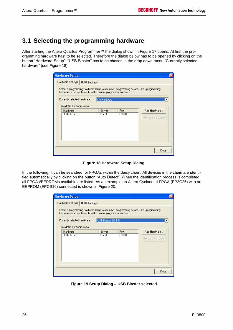
3.1 Selecting the programming hardware
After starting the Altera Quartus Programmer™ the dialog shown in Figure 17 opens. At first the pro-
gramming hardware hast to be selected. Therefore the dialog below has to be opened by clicking on the
button “Hardware-Setup”. “USB-Blaster” has to be chosen in the drop down menu “Currently selected
hardware” (see Figure 18).
Figure 18 Hardware Setup Dialog
In the following, it can be searched for FPGAs within the daisy chain. All devices in the chain are identi-
fied automatically by clicking on the button “Auto Detect”. When the identification process is completed,
all FPGAs/EEPROMs available are listed. As an example an Altera Cyclone III FPGA (EP3C25) with an
EEPROM (EPCS16) connected is shown in Figure 20.
Figure 19 Setup Dialog – USB Blaster selected

Altera Quartus II Programmer™
EL9800 27
Figure 20 Quartus II Programmer Dialog after „Auto-Detect“ processing
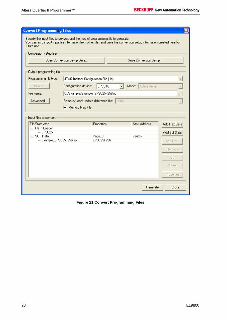
3.2 Conversion of a SOF-File in the JIC-file format
In the example the EEPROM, connected with the FPGA, can be programmed using the “JTAG-Indirect”
Mode exclusively. Therefore the binary files generated from the Altera Quartus II™ have to be converted
in the JIC-format before programming of the EEPROM can take place. Selecting the “File” menu and
choosing „Convert Programming File…“ the „Convert Programming Files…” dialog (see Figure 21) is
opened. FPGA type, EEPROM, source and destination file format have to be set before the conversion
process can be started.
The steps below have to be followed to convert the programming file in the JIC-format:
1. „Programming file type“ JTAG Indirect Configuration File (.jic) auswählen
2. „Configuration device:“ EPCS16 (In case of the EtherCAT postage stamp FB1122)
3. „File Name:“ File and path name of the JIC-file has to be entered here.
4. Select „Flash Loader“ and click on „Add Device“. At this point select the FPAG-Type, which in this
case is the Cyclone III EP3C25.
5. Select „SOF Data“ and click on „Add File“ to select the SOF source file.
6. Start the conversion process by clicking on „Generate“ and confirm opening messages.
Altera Quartus II Programmer™
28 EL9800
Figure 21 Convert Programming Files

Altera Quartus II Programmer™
EL9800 29
3.3 Choosing the programming file
After successful conversion of the SOF-file, the programming of the EEPROM can take place. As shown
in Figure 22the EEPROM (EPCS16) has to be chosen. The programming file has then to be set by click-
ing on the button “Change File”.
Figure 22 Selection of the programming file
The last step is to configure the programming process, by setting check marks on “Program/Configure”
and “Verify”.
3.4 Programming of the FPGA/EEPROM
The programming process is then started by clicking on the button „Start“. In the message field the pro-
gramming process is logged. And in case of a faulty programming process an error message is displayed
in this field.

Appendix
30 EL9800
4 Appendix
4.1 Support and Service
Beckhoff and their partners around the world offer comprehensive support and service, making available
fast and competent assistance with all questions related to Beckhoff products and system solutions.
4.1.1 Beckhoff's branch offices and representatives
Please contact your Beckhoff branch office or representative for local support and service on Beckhoff
products!
The addresses of Beckhoff's branch offices and representatives round the world can be found on her
internet pages: http://www.beckhoff.com
You will also find further documentation for Beckhoff components there.
4.2 Beckhoff Headquarters
Beckhoff Automation GmbH
Eiserstr. 5
33415 Verl
Germany
phone: + 49 (0) 5246/963-0
fax: + 49 (0) 5246/963-198
e-mail: [email protected]
web: www.beckhoff.com
Beckhoff Support
Support offers you comprehensive technical assistance, helping you no only with the application of indi-
vidual Beckhoff products, but also with other, wide-ranging services:
support
design, programming and commissioning of complex automation systems
and extensive training program for Beckhoff system components
hotline: + 49 (0) 5246/963-157
fax: + 49 (0) 5246/963-9157
e-mail: [email protected]
Beckhoff Service
The Beckhoff Service Center supports you in all matters of after-sales service:
on-site service
repair service
spare parts service
hotline service
hotline: + 49 (0) 5246/963-460
fax: + 49 (0) 5246/963-479
e-mail: [email protected]