Efficient three-color white organic light-emitting diodes ...
6
Efficient three-color white organic light-emitting diodes with a spaced multilayer emitting structure Fei Yan, Guichuan Xing, Rui Chen, Hilmi Volkan Demir, Handong Sun, Tze Chien Sum, and Xiao Wei Sun Citation: Applied Physics Letters 106, 023302 (2015); doi: 10.1063/1.4905599 View online: http://dx.doi.org/10.1063/1.4905599 View Table of Contents: http://scitation.aip.org/content/aip/journal/apl/106/2?ver=pdfcov Published by the AIP Publishing Articles you may be interested in Using interlayer step-wise triplet transfer to achieve an efficient white organic light-emitting diode with high color- stability Appl. Phys. Lett. 104, 193303 (2014); 10.1063/1.4876215 Full phosphorescent white-light organic light-emitting diodes with improved color stability and efficiency by fine tuning primary emission contributions AIP Advances 4, 027103 (2014); 10.1063/1.4865209 Organic light-emitting diodes for lighting: High color quality by controlling energy transfer processes in host- guest-systems J. Appl. Phys. 111, 033102 (2012); 10.1063/1.3679549 Color control of multilayer stacked white polymer light-emitting diodes using a quantum dot as an interlayer Appl. Phys. Lett. 94, 093303 (2009); 10.1063/1.3079814 Efficient nondoped white organic light-emitting diodes based on electromers Appl. Phys. Lett. 89, 123503 (2006); 10.1063/1.2357008 This article is copyrighted as indicated in the article. Reuse of AIP content is subject to the terms at: http://scitation.aip.org/termsconditions. Downloaded to IP: 139.179.65.117 On: Thu, 15 Jan 2015 09:30:34
Transcript of Efficient three-color white organic light-emitting diodes ...

Efficient three-color white organic light-emitting diodes with a spaced multilayeremitting structureFei Yan, Guichuan Xing, Rui Chen, Hilmi Volkan Demir, Handong Sun, Tze Chien Sum, and Xiao Wei Sun Citation: Applied Physics Letters 106, 023302 (2015); doi: 10.1063/1.4905599 View online: http://dx.doi.org/10.1063/1.4905599 View Table of Contents: http://scitation.aip.org/content/aip/journal/apl/106/2?ver=pdfcov Published by the AIP Publishing Articles you may be interested in Using interlayer step-wise triplet transfer to achieve an efficient white organic light-emitting diode with high color-stability Appl. Phys. Lett. 104, 193303 (2014); 10.1063/1.4876215 Full phosphorescent white-light organic light-emitting diodes with improved color stability and efficiency by finetuning primary emission contributions AIP Advances 4, 027103 (2014); 10.1063/1.4865209 Organic light-emitting diodes for lighting: High color quality by controlling energy transfer processes in host-guest-systems J. Appl. Phys. 111, 033102 (2012); 10.1063/1.3679549 Color control of multilayer stacked white polymer light-emitting diodes using a quantum dot as an interlayer Appl. Phys. Lett. 94, 093303 (2009); 10.1063/1.3079814 Efficient nondoped white organic light-emitting diodes based on electromers Appl. Phys. Lett. 89, 123503 (2006); 10.1063/1.2357008
This article is copyrighted as indicated in the article. Reuse of AIP content is subject to the terms at: http://scitation.aip.org/termsconditions. Downloaded to IP:
139.179.65.117 On: Thu, 15 Jan 2015 09:30:34
Efficient three-color white organic light-emitting diodes with a spacedmultilayer emitting structure
Fei Yan,1 Guichuan Xing,2 Rui Chen,2,3 Hilmi Volkan Demir,1,2 Handong Sun,2,4,a)
Tze Chien Sum,2,a) and Xiao Wei Sun1,a)
1LUMINOUS! Center of Excellence for Semiconductor Lighting and Displays, School of Electricaland Electronic Engineering, Nanyang Technological University, 50 Nanyang Avenue, Singapore 6397982Division of Physics and Applied Physics, School of Physical and Mathematical Sciences, NanyangTechnological University, Singapore 6373713Department of Electrical and Electronic Engineering, South University of Science and Technology of China,Shenzhen, Guangdong 518055, People’s Republic of China4Centre for Disruptive Photonic Technologies (CDPT), Nanyang Technological University, Singapore,Singapore 637371
(Received 21 October 2014; accepted 26 December 2014; published online 12 January 2015)
By employing a spaced multilayer structure in a uniformly mixed P and N co-host, we developed a
three-color white organic light emitting device with a stable Commission Internationale de
L’Eclairage coordinates insensitive to the applied bias voltage. This insensitivity was achieved by
suppressing the exciton quenching and shifting recombination zone effectively. Besides the achieved
stable color coordinates of (0.411 6 0.007, 0.382 6 0.003), a high power efficiency of 30.7 lm/W and
high color rendering index >80 were realized simultaneously. VC 2015 AIP Publishing LLC.
[http://dx.doi.org/10.1063/1.4905599]
As a new technology in flat panel displays, organic
light-emitting diode (OLED) displays have achieved a great
success, which have been visibly demonstrated by the com-
mercial 5500 TV manufactured by LG and Samsung.1–10 As
the next important application, OLED lighting is lags behind
relatively in the commercial aspect. Although white OLED
(WOLED) has not demonstrated itself as a lighting device in
the commercial market, it is actually used for the state-of-
the-art OLED TV-despite of the patterning difficulty in
OLED displays.11 Thus, it is interesting to recognize that
OLED display and WOLED lighting are becoming one tech-
nology, and their development will converge. The require-
ments for WOLED include high power efficiency under high
luminance (namely, high luminous efficiency and low driv-
ing voltage), high color rendering index (CRI), and voltage
independent emission spectra.1–10
To achieve white emission, there are mainly two scenarios.
The first is the device with one white emissive layer doped with
red (R), green (G), and blue (B) dopants. While the other one is
the device containing stacked RGB emissive sub-layers.
Considering both display and lighting applications, the latter
one becomes the present choice.7,8,12–14 Normally, the mobili-
ties of electron and hole differ by orders of magnitude or
even worse for various functional layers in the OLED structure,
and they are electrical field dependent.15,16 As a result, the
recombination zone shifts with the change of driving voltage,
leading to voltage dependent emissive spectra.8,12,13 Generally,
it is difficult to obtain satisfactory performance for the parame-
ters mentioned above for WOLED in the same device
simultaneously.8,12,13 If the recombination zone could cover
RGB emissive sub-layers uniformly at any driving voltage, the
emission could be engineered to be bias-insensitive. But for
conventional structures, the recombination zone cannot extend
to all the emissive sub-layers uniformly unless the thicknesses
of the RGB emissive sub-layers could be decreased. However
as the thickness reduces, the amount of dopant molecules is
also decreased, leading to a significant drop of luminance and
efficiency. In this work, we designed and realized a spaced mul-
tilayer structure (SMS) device, exhibiting high efficiency, stable
spectra, and high CRI simultaneously.
All chemicals used in this work are commercially available.
Patterned indium tin oxide (ITO) glass substrates (10 X/sq.)
were used in our experiments. First, the ITO substrates were
cleaned with de-ionized water, isopropanol, acetone in
sequence. Then they were oven-dried and treated in O2
plasma. All functional films and aluminum electrode were
fabricated by thermal evaporation in a single run at a base
pressure of less than 4� 10�4 Pa without breaking the vac-
uum. All the organics and other compounds were evaporated
at a rate of about 0.1–0.2 nm s�1, and the aluminum electro-
des were evaporated at a rate of 0.8–1 nm s�1. A shadow
mask was used to define the cathode and we could obtain
eight devices (with emissive area of 4 � 4 mm2) on each sub-
strate. The luminance-current-voltage (L-I-V) characteristics
and electroluminescence (EL) spectra were measured simul-
taneously with a Keithley 2400 source meter and a
Photoresearch PR-650 spectrometer. For transient photolu-
minescence (PL) experiment, the laser source was Coherent
LibraTM
regenerative amplifier (50 fs, 1 KHz, 800 nm) seeded
by a Coherent VitesseTM
oscillator (50 fs, 80 MHz). 325-nm
laser pulses were generated from the Coherent OPerA-Solo
optical parametric amplifier. The laser pulses (circular spot,
diameter 1.5 mm) were directed to the films. The emission
from the samples was collected at a backscattering angle of
150� by a pair of lenses into an Optronis OptoscopeTM
streak
camera system which has an ultimate temporal resolution of
a)Authors to whom correspondence should be addressed. Electronic addresses:
[email protected], [email protected], and [email protected]
0003-6951/2015/106(2)/023302/5/$30.00 VC 2015 AIP Publishing LLC106, 023302-1
APPLIED PHYSICS LETTERS 106, 023302 (2015)
This article is copyrighted as indicated in the article. Reuse of AIP content is subject to the terms at: http://scitation.aip.org/termsconditions. Downloaded to IP:
139.179.65.117 On: Thu, 15 Jan 2015 09:30:34

�10 ps. All measurements were carried out at room tempera-
ture in ambient atmosphere.
Both P and N doping were applied to the charge injec-
tion layers to lower down the driving voltage and enhance
the power efficiency; 4,40,400-tris(N-3-methyphenyl-N-phenyl-
amino)triphenylamine (m-MTDATA) doped with 2,3, 5,6-
tetrafluoro-7,7,8,8-tetracyanoquinodimethane (F4-TCNQ), and
3,5-Tris(1-phenyl-1H-benziMidazol-2-yl)benzene (TPBi) doped
with cesium carbonate (Cs2CO3) were used as P-type hole
injection and N-type electron injection layer, respectively.
For the emissive layer (EML), a blended film of 4,40,400-Tri-
9-carbazolyltriphenylamine (TCTA) and TPBi with a 1:1
weight ratio was employed as the PN co-host for better
charge balance. The phosphorescent materials of bis(1-phe-
nyl-isoquinoline)(acetylacetonato)iridium(III) (Ir(piq)2 acac)
and bis(3,5-difluoro-2–(2-pyridyl)phenyl-(2-arboxypyridyl)
iridium(III) (FIrpic) were selected as red and blue emitting
dopants, respectively. In order to obtain a high CRI white
emissive spectrum, the bis(2-phenylbenzothiazolato)(acetyl
acetonate)iridium(III) ((BT)2Iracac) was selected as the
complementary yellow emitting dopant. The hole transport ma-
terial used was N,N0-di(naphthalene-1-yl)-N,N0-iphenyl-benzi-
dine (NPB).
The PN co-host is supposed to have a broader recombi-
nation zone compared to single host, resulting in a lower
concentration of both polarons and excitons.17,18 Furthermore,
the broader emission zone is beneficial to cover multi mono-
chromic emission sub-layer in the WOLEDs for a voltage in-
dependent emissive spectrum. In order to investigate the
influence of SMS comparing to normal emissive structure,
we fabricated the blue monochrome emissive device before
the WOLEDs. Four OLEDs of the PN co-host structure were
fabricated and compared (Fig. 1); Device i: ITO\m-
MTDATA:F4-TCNQ (5% wt., 30 nm)\NPB (15 nm)\TCTA
(15 nm)\EMi\TPBi (30 nm)\TPBi:Cs2CO3 (10% wt., 30 nm)
\Al (100 nm), where i¼ 1, 2, 3, and 4. The structures of all
EMi are indicated in Table I. The R, Y, and B represent the
red TcTa:TPBi:Ir(piq)2acac (1:1:x% wt.), yellow TCTA:
TPBi:(BT)2Iracac (1:1:x% wt.), and blue TCTA:TPBi:
FIrpic (1:1:x% wt.) emissive sub-layer, respectively. In the
devices with the SMS, the host of TCTA:TPBi (1:1 wt) film
between the emitting layers was also called spacer (S).
Device 1 is a monochrome control device with a normal
guest-host structure. Device 2 is another monochrome con-
trol device with the SMS. Device 3 is the three-color white
device with the SMS. Device 4 is the target three-color white
device based on device 3. For all devices, the amount of all
three color dopant molecules is the same.
Fig. 2 shows the plots of current density-voltage, lumi-
nous efficiency-luminance, and power efficiency-luminance
of devices 1, 2, 3, and 4. For the monochrome OLED device
1, the onset driving voltage (at about 1 cd/m2) was about
2.6 V (Fig. 2), which is close to the photon energy radiated
from FIrpic exciton (478 nm). Due to the P and N doped
injection layers and uniform host, there is almost no energy
barrier for holes and electrons to inject and transport.
Additionally, because of a better charge balance of the P and
N co-host, the device shows a maximum luminous efficiency
of about 37.3 cd/A at 150 cd/m2 and a maximum power effi-
ciency of about 42.1 lm/W at 3.5 cd/m2. Comparing to device
1, the maximum luminous efficiency of device 2 with the
SMS is 35.9 cd/A at 143 cd/m2, slightly lower compared to
device 1, which is probably caused by the backward energy
transfer from FIrpic exciton to TPBi (triplet state of 2.6 eV)
molecule in the spacer between two emissive sub-layers.7
Additionally, the driving voltage of device 2 with the SMS is
FIG. 1. The structures of devices 1, 2, 3, and 4.
TABLE I. The EM structure of all devices. The R, Y, and B represent the
red TcTa:TPBi:Ir(piq)2acac (1:1:x% wt.), yellow TCTA:TPBi:(BT)2Iracac
(1:1:x% wt.), and blue TCTA:TPBi:FIrpic (1:1:x% wt.) emissive sub-layer,
respectively.
Device Emissive layer structure
EM1 B (7% wt., 20 nm)
EM2 [B (7% wt., 3.5 nm)\S (3 nm)]*5\B (7% wt., 2.5 nm)
EM3 R (7% wt., 3 nm)\S (3 nm)\Y (7% wt., 3 nm)\S (3 nm)\B
(7% wt., 4 nm)\S (3 nm)\R (7% wt., 3 nm)\S (3 nm)\Y
(7% wt., 3 nm)\S (3 nm)\B (7% wt., 4 nm)
EM4 B (7% wt., 5 nm)\S (2 nm)\R (5% wt., 2 nm)\S (2 nm)\Y
(5% wt., 2 nm)\S (2 nm)\B (7% wt., 3 nm)\S (2 nm)\Y
(5% wt., 1.5 nm)\S (2 nm)\R (5% wt., 1.5 nm)\S (2 nm)\B
(7% wt., 2 nm)\S (2 nm)\Y (5% wt., 0.5 nm)\S (2 nm)\R
(5% wt., 0.5 nm)\S (2 nm)\B (10% wt., 2 nm).
FIG. 2. The current density-voltage and luminous efficiency-luminance
curves of devices 1, 2, 3, and 4. The power efficiency plots versus luminance
of devices 1, 2, 3, and 4 are shown in inset.
023302-2 Yan et al. Appl. Phys. Lett. 106, 023302 (2015)
This article is copyrighted as indicated in the article. Reuse of AIP content is subject to the terms at: http://scitation.aip.org/termsconditions. Downloaded to IP:
139.179.65.117 On: Thu, 15 Jan 2015 09:30:34
slightly higher comparing to device 1, which is related to
more interfaces of the SMS. The maximum power efficiency
of device 2 was 39.6 lm/W at 3.3 cd/m2. However, it is note
that the luminous efficiency drop for device 2 (dropped by
21% from 35.9 cd/A at 143 cd/m2 to 28.2 cd/A at 11290 cd/
m2) at high luminance was improved significantly compared
to device 1 (dropped by 36% from 37.3 cd/A at 150 cd/m2 to
26.1 cd/A at 10470 cd/m2). Though the amount of monochromic
dopant molecules is the same for devices 1 and 2, and the
concentration of dopant for each emissive sub-layer in de-
vice 2 is also the same to device 1, due to the spaced recom-
bination zone structure, the distance between two Ir-complex
dopants divided by the spacer exceeds the effective radius of
exiton-exciton interactions (Fig. 1). Thus, the triplet-triplet
exciton annihilation process caused by exciton-exciton inter-
action, especially under higher driving current density, was
suppressed effectively, leading to a slower luminous effi-
ciency roll-off.17–19 In order to compare the luminous effi-
ciency droop between devices 1 and 2, following Baldo
et al.,20 we defined a critical current density (J0) as the lumi-
nous efficiency drop to 70% of the maximum value. As indi-
cated in Fig. 2, for device 1, J0 is about 40 mA/cm2 when the
luminous efficiency is 26.1 cd/A (the corresponding maxi-
mum luminous efficiency is 37.3 cd/A at 0.2 mA/cm2).
While for device 2 with SMS, J0 is about 80 mA/cm2 when
the luminous efficiency is 24.5 cd/A, compared to the maxi-
mum luminous efficiency of 35.8 cd/A at 0.4 mA/cm2.
Based above works the three-color white device 3 with
the SMS was fabricated, and the maximum luminous effi-
ciency is about 32.2 cd/A at 64.5 cd/m2 (dropped by 24.8%
to 24.2 cd/A at 9690 cd/m2) (Fig. 2), which is comparatively
smaller than those of devices 1 and 2. The maximum power
efficiency was about 36.8 lm/W at 3.1 cd/m2 and it decreased
to 12.5 lm/W at 9690 cd/m2, which accounts for about 66%
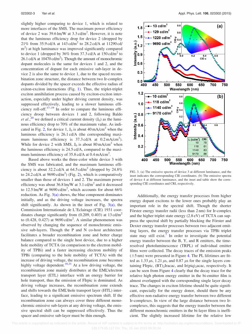
reduction. As Fig. 3(a) shows, the blue component dominates
initially, and as the driving voltage increases, the spectra
shift significantly. As shown in the inset of Fig. 3(a), the
Commission Internationale de L’Eclairage (CIE) 1931 coor-
dinates change significantly from (0.209, 0.403) at 13 cd/m2
to (0.428, 0.427) at 9690 cd/m2. A similar phenomenon was
observed by changing the sequence of monochromic emis-
sive sub-layers. Though the P and N co-host architecture
facilitates a broader recombination zone and better charge
balance compared to the single host device, due to a higher
hole mobility of TCTA (in comparison to the electron mobil-
ity of TPBi) and a faster increasing electron mobility of
TPBi (comparing to the hole mobility of TCTA) with the
increase of driving voltage, the recombination zone becomes
highly voltage dependent.18,21 At a low driving voltage, the
recombination zone mainly distributes at the EML\electron
transport layer (ETL) interface with an energy barrier for
hole transport, thus the emission of FIrpic is dominated. As
driving voltage increases, the recombination zone extends
and shifts towards the EML\hole transport layer (HTL) inter-
face, leading to a significant emissive spectrum shift. If the
recombination zone can always cover three different mono-
chromic emissive sub-layers at any driving voltage, the emis-
sive spectral shift can be suppressed effectively. Thus the
spacer and emissive sub-layer must be thin enough.
Additionally, the energy transfer processes from higher
energy dopant excitons to the lower ones probably play an
important role in the spectral shift. Though the shorter
F€orster energy transfer radii (less than 2 nm) for Ir-complex
and the higher triplet state energy (2.8 eV) of TCTA can sup-
press the spectral shift by partially blocking the F€orster and
Dexter energy transfer processes between two adjacent emit-
ting layers, the energy transfer processes via TPBi triplet
state may still exist.7 In order to investigate the potential
energy transfer between the B, Y, and R emitters, the time-
resolved photoluminescence (TRPL) of individual emitter
films were collected. The decay traces of the emission peaks
(65 nm) were presented in Figure 4. The PL lifetimes are fit-
ted as 1.33 ls, 1.21 ls, and 0.87 ls for the single layers con-
taining FIrpic, (BT)2Iracac, and Ir(piq)2acac, respectively. It
can be seen from Figure 4 clearly that the decay trace for the
relative high photon energy emitter in the bi-emitter film is
almost overlapped with the corresponding single layer decay
trace. The changes in exciton lifetime should be quite signifi-
cant, especially for the energy donor, should there be any
effective non-radiative energy transfer between two different
Ir-complexes. In view of the large distance between two Ir-
complexes, this suggests that the energy transfer between the
different monochromic emitters in the bi-layer films is ineffi-
cient. The slightly increased lifetime for the relative low
FIG. 3. (a) The emissive spectra of device 3 at different luminance, and the
inset indicates the corresponding CIE coordinates. (b) The emissive spectra
of device 4 at different luminance, and the inset and table show the corre-
sponding CIE coordinates and CRI, respectively.
023302-3 Yan et al. Appl. Phys. Lett. 106, 023302 (2015)
This article is copyrighted as indicated in the article. Reuse of AIP content is subject to the terms at: http://scitation.aip.org/termsconditions. Downloaded to IP:
139.179.65.117 On: Thu, 15 Jan 2015 09:30:34

photon energy emitter in the bi-emitter film should be caused
by the relative high energy photon re-absorbed by this
emitter.22
To weaken the spectral shift caused by the recombina-
tion zone shift and re-absorption of lower emitters, the thick-
ness of emissive sub-layers and spacer were reduced for
device 4 compared to device 3. Furthermore, in order to
weaken the influence of non-radiative energy transfer pro-
cess, the amounts of all monochromic dopant in the emissive
sub-layers were adjusted, and the optimized three-color
white device 4 was designed and fabricated. Because there is
a relatively thicker and larger energy barriers for electron
and hole at EML\HTL and EML\ETL interfaces, respec-
tively, the charge and exciton densities are correspondingly
larger. Thus, we allocated the two blue monochromic layers
at these two interfaces to ensure the relative intensity of
FIrpic compared to the other two components. Similarly, in
order to weaken the likely influence of non-radiative energy
transfer, the sequence of the monochromic layers were also
adjusted to ensure the spectral stability. From the spectral
shift indicated in Fig. 3(a) and emission layer structure of de-
vice 3 (Fig. 1), the recombination zone width was extended
from less than 9 nm to more than 16 nm. A spacer thickness
of 2 nm was selected for in device 4, which is to balance the
spectral shift caused by recombination zone shift and energy
transfer between different emissive excitons. To ensure a stable
emission of blue color as the driving voltage varies, the FIrpic
concentration of the emissive sub-layer close to EML\ETL
interface was increased to 10% wt., and the amount of FIrpic in
the whole emissive layer is more than those of (BT)2Iracac and
Ir(piq)2acac. As Fig. 2 shows, device 4 exhibits a maximum lu-
minous efficiency of about 29.7 cd/A at 118 cd/m2, which
reduces to 22.9 cd/A at 9170 cd/m2. The corresponding drop is
about 22%. The power efficiency of the device is 30.7 lm/W at
5.7 cd/m2 and 11.7 lm/W at 9170 cd/m2, which accounts for
60% drop. As shown in Fig. 3(b), the CIE 1931 coordinates of
device 4 fall in the warm white range. As the driving voltage
varies, coordinates (0.411 6 0.007, 0.382 6 0.003) have a little
change as the luminance increases from about 10 cd/m2 to about
10 000 cd/m2. Additionally, the CRIs at various luminance are
also excellent as indicated in the inset table in Fig. 3(b); at about
10 000 cd/m2, the CRI is 86.
In conclusion, employing P and N doped charge injec-
tion layer, P and N co-host, and SMS emissive layer, a
three-color WOLED was developed, which exhibited a good
overall performance, including high power efficiency, slower
efficiency roll off at high luminance, stable emissive spectra,
and high CRI.
This work was financially supported by National Research
Foundation of Singapore (Grant Nos. NRF-CRP11-2012-01
and NRF-CRP6-2010-2).
1S. Kalluri, R. R. Jerry, and C. Charles, in Conference on Head- and
Helmet-Mounted Displays XVII/Conference on Display Technologies and
Applications for Defense, Security, and Avionics VI, Baltimore, MD,
25–26 April 2012.2Z. Ma, P. Sonar, and Z. Chen, Curr. Org. Chem. 14, 2034–2069 (2010).3A. Laaperi, J. Soc. Inf. Disp. 16, 1125–1130 (2008).4O. N. Ermakov, M. G. Kaplunov, O. N. Efimov, and S. A. Stakharny,
Proc. SPIE 6636, A6360 (2007).5Y. L. Lei, Y. Jin, D. Y. Zhou, W. Gu, X. B. Shi, L. S. Liao, and S. T. Lee,
Adv. Mater. 24, 5345 (2012).6H. Sasabe, J. Takamatsu, T. Motoyama, S. Watanabe, G. Wagenblast, N.
Langer, O. Molt, E. Fuchs, C. Lennartz, and J. Kido, Adv. Mater. 22,
5003–5007 (2010).7S. Reineke, F. Lindner, G. Schwartz, N. Seidler, K. Walzer, B. L€ussem,
and K. Leo, Nature 459, 234–238 (2009).8C. Murawski, K. Leo, and M. C. Gather, Adv. Mater. 25, 6801–6827
(2013).9B. W. D’Andrade and S. R. Forrest, Adv. Mater. 16, 1585–1595 (2004).
10B. W. D’Andrade, J. Brooks, V. Adamovich, M. E. Thompson, and S. R.
Forrest, Adv. Mater. 14, 1032–1036 (2002).
FIG. 4. The transient photoluminescence plots of (a) Firpic in film A and D
(monitored at 478 nm), and (BT)2Iracac in films B and D (monitored at
560 nm), (b) Firpic in films A and E (monitored at 478 nm), and Ir(piq)2acac
in films C and E (monitored at 620 nm), (c) (BT)2Iracac in films B and F
(monitored at 560 nm), and Ir(piq)2acac in films C and F (monitored at
620 nm). The solid lines are correspondingly fitting curves. The R, Y, and B
represent the TcTa:TPBi:Ir(piq)2acac (1:1:7% wt.), TCTA:TPBi:(BT)2Iracac
(1:1:7% wt.), and TCTA:TPBi:FIrpic (1:1:7% wt.) film, respectively.
023302-4 Yan et al. Appl. Phys. Lett. 106, 023302 (2015)
This article is copyrighted as indicated in the article. Reuse of AIP content is subject to the terms at: http://scitation.aip.org/termsconditions. Downloaded to IP:
139.179.65.117 On: Thu, 15 Jan 2015 09:30:34

11C. W. Han, K. M. Kim, S. J. Bae, H. S. Choi, J. M. Lee, T. S. Kim, Y. H.
Tak, S. Y. Cha, and B. C. Ahn, Dig. Tech. Pap. - Soc. Inf. Disp. Int. Symp.
43, 279–281 (2012).12M. C. Gather, R. Alle, H. Becker, and K. Meerholz, Adv. Mater. 19, 4460 (2007).13A. K€ohnen, K. Meerholz, M. Hagemann, M. Brinkmann, and S. Sinzinger,
Appl. Phys. Lett. 92, 33305 (2008).14B. Zhao, Z. Su, W. Li, B. Chu, F. Jin, X. Yan, T. Zhang, F. Zhang, D. Fan,
Y. Gao, J. Wang, H. Pi, and J. Zhu, Nanoscale Res. Lett. 8, 529 (2013).15A. K€ohler, Nat. Mater. 11, 836–837 (2012).16I. I. Fishchuk, A. Kadashchuk, M. Ullah, H. Sitter, A. Pivrikas, J. Genoe,
and H. B€assler, Phys. Rev. B 86, 045207 (2012).
17S. Lee, K. Kim, D. Limbach, Y. Park, and J. Kim, Adv. Funct. Mater. 23,
4105–4110 (2013).18S. Kim, J. Jang, K. Yook, and J. Lee, Appl. Phys. Lett. 92, 023513
(2008).19M. Gather, A. K€ohnen, and K. Meerholz, Adv. Mater. 23, 233–248
(2011).20M. A. Baldo, C. Adachi, and S. R. Forrest, Phys. Rev. B 62, 10967 (2000).21L. Xia, Z. Chen, B. Qu, J. Luo, S. Kong, Q. Gong, and J. Kido, Adv.
Mater. 23, 926–952 (2011).22M. I. Sluch, A. S. Averjushkin, O. I. Tolstikhin, and A. G. Vitukhnovsky,
Phys. Scr. 50, 585 (1994).
023302-5 Yan et al. Appl. Phys. Lett. 106, 023302 (2015)
This article is copyrighted as indicated in the article. Reuse of AIP content is subject to the terms at: http://scitation.aip.org/termsconditions. Downloaded to IP:
139.179.65.117 On: Thu, 15 Jan 2015 09:30:34