Efficient Carry Generation Technique Incorporating
16
-
Upload
gokul-krishnan -
Category
Documents
-
view
218 -
download
0
Transcript of Efficient Carry Generation Technique Incorporating

8/7/2019 Efficient Carry Generation Technique Incorporating
http://slidepdf.com/reader/full/efficient-carry-generation-technique-incorporating 1/16

8/7/2019 Efficient Carry Generation Technique Incorporating
http://slidepdf.com/reader/full/efficient-carry-generation-technique-incorporating 2/16
` Dynamic power consumption is a major concern for designing various modern
age information systems and computers.
` Recent advances in low power VLSI design results in charge recovery based
adiabatic logic concept, which proves to be a potential parametric to design
CMOS circuits for various low power applications.
` Research in this domain is fueled by the fact that instead of discharging the
load capacitance to ground, the charge flows back to power supply and can be
reused.
` Keeping the advantages of energy recovery logic in mind, we demonstrate low
energy carry break logic exploiting certain aspects of carry generation based on
the bit positions in input vectors.
` Design has been implemented in 90 nm TSMC process, showing 70%
improvement in power.

8/7/2019 Efficient Carry Generation Technique Incorporating
http://slidepdf.com/reader/full/efficient-carry-generation-technique-incorporating 3/16
` E nergy E fficiency has been a major design concern in various high performance
and mobile computing systems over the past few years.
` Consequently, several approaches have been developed to improve Power metric.
` Adiabatic Logic category is a powerful contrivance in growing low power domain
which performs computation in reversible manner, leads to potentially zero energy
consumption with the use of AC Power supply.
` Ideally in adiabatic logic, each charge could be recycled infinite number of times,
but practically, it is not possible because of the energy loss due to the switching
resistance of the transistors.
` In this work, we present a carry generation logic circuit for adders which shows a
good improvement in power consumption, taking various advantages introduced
by adiabatic logic into account.

8/7/2019 Efficient Carry Generation Technique Incorporating
http://slidepdf.com/reader/full/efficient-carry-generation-technique-incorporating 4/16
` CMOS transistors dissipate power when they switch while charging and
discharging the capacitance C through a component having resistivity R.
` The energy dissipated when charging of the gate is proportional to R.C *CV2
where T is the time it takes the gate to charge or discharge.
` The constant of proportionality depends on the slope of power clock voltage
signal waveform. In non-reversible circuits, the charging time T is proportional to
RC.
` Reversible logic uses the fact that a single clock cycle is much longer then RC
and thus attempts to spread the charging of the gate over the whole cycle and
thus reduces the energy dissipated.
T

8/7/2019 Efficient Carry Generation Technique Incorporating
http://slidepdf.com/reader/full/efficient-carry-generation-technique-incorporating 5/16
` Ideally then, by increasing the time T over which computation is performed andby using reversible logic to avoid the destruction of information, it should bepossible to create a circuit which computes with vanishingly low energydissipation as the time allowed for that computation extends indefinitely.
` That¶s why we should avoid using adiabatic while going for faster designs. Inorder to extend the charging time of the gate we make sure never to turn on atransistor that has a potential difference between source and drain, andfurthermore, once the transistor is turned on, energy flows through it in a
gradual and controlled manner [1].` The second rule that adiabatic circuits must follow is never to turn off a
transistor when there is current flowing through it.` The reason for this follows from the fact that transistors are not perfect switches
going from on to off instantly. Instead, it gradually changes from on to off withthe speed at which the gate voltage changes.
` Thus the transistor is in an ³in between´ state for a long period of time. Duringthis time, the voltage drop across the transistor greatly increases yet theresistance is not high enough to bring power dissipation to zero.
` Thus source-drain voltage can be changed only when the device is OFF.
8/7/2019 Efficient Carry Generation Technique Incorporating
http://slidepdf.com/reader/full/efficient-carry-generation-technique-incorporating 6/16
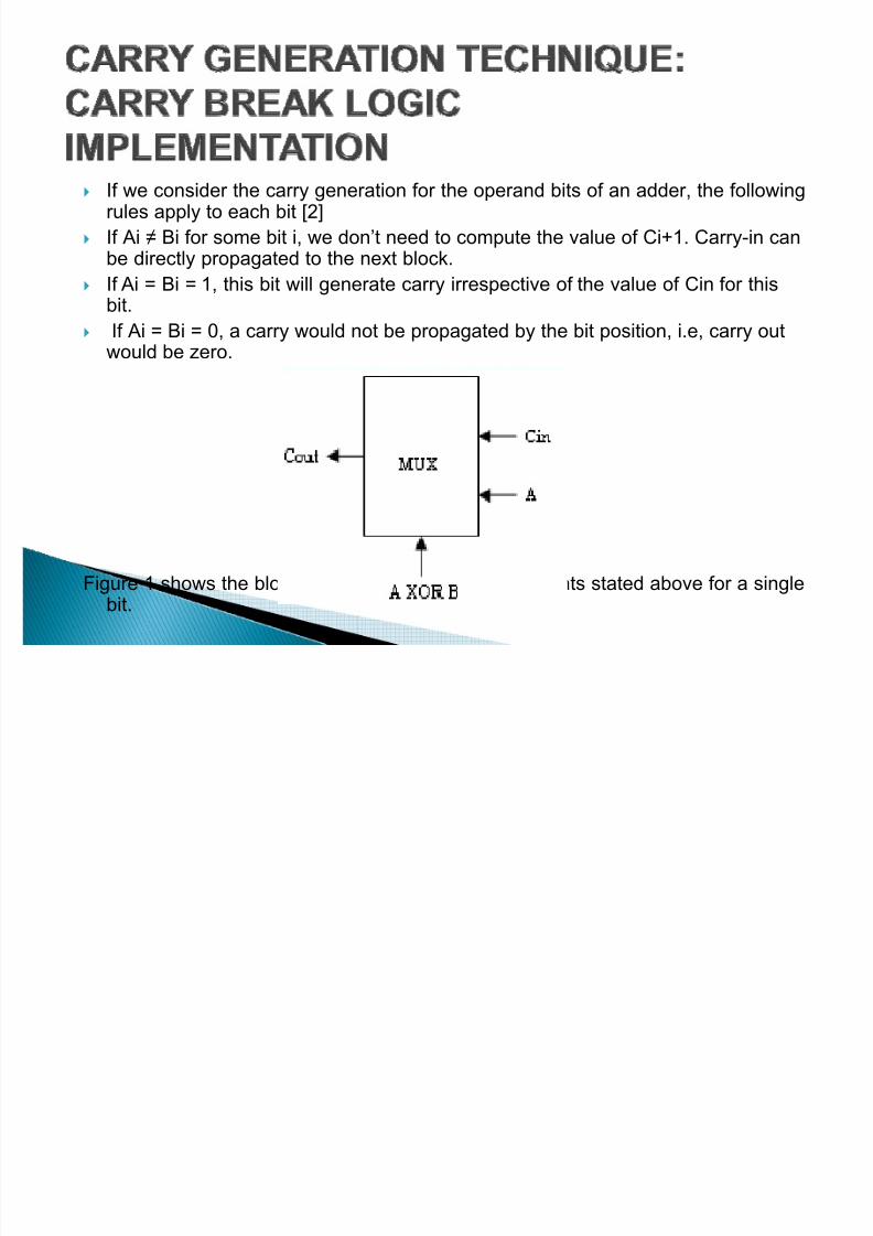
` If we consider the carry generation for the operand bits of an adder, the followingrules apply to each bit [2]
` If Ai Bi for some bit i, we don¶t need to compute the value of Ci+1. Carry-in canbe directly propagated to the next block.
` If Ai = Bi = 1, this bit will generate carry irrespective of the value of Cin for thisbit.
` If Ai = Bi = 0, a carry would not be propagated by the bit position, i.e, carry outwould be zero.
Figure 1 shows the block representation of the statements stated above for a single
bit.

8/7/2019 Efficient Carry Generation Technique Incorporating
http://slidepdf.com/reader/full/efficient-carry-generation-technique-incorporating 7/16
` Thus for large operands, there is no need to wait for the carry from the previous lock. Itcan be ³broken´ at bit positions where Ai=Bi. In other words, carry in can beasynchronously set to µ1¶ for the (i+1)-bit if Ai=Bi=1and µ0¶ if Ai=Bi=0.
Figure 2 shows block diagram for four-bit MCBA [5] slice that consists of three types of blocks
8/7/2019 Efficient Carry Generation Technique Incorporating
http://slidepdf.com/reader/full/efficient-carry-generation-technique-incorporating 8/16
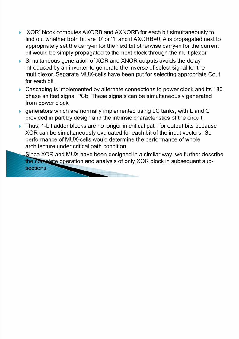
` µXOR¶ block computes AXORB and AXNORB for each bit simultaneously to
find out whether both bit are µ0¶ or µ1¶ and if AXORB=0, A is propagated next toappropriately set the carry-in for the next bit otherwise carry-in for the currentbit would be simply propagated to the next block through the multiplexor.
` Simultaneous generation of XOR and XNOR outputs avoids the delayintroduced by an inverter to generate the inverse of select signal for themultiplexor. Separate MUX-cells have been put for selecting appropriate Cout
for each bit.` Cascading is implemented by alternate connections to power clock and its 180
phase shifted signal PCb. These signals can be simultaneously generatedfrom power clock
` generators which are normally implemented using LC tanks, with L and Cprovided in part by design and the intrinsic characteristics of the circuit.
` Thus, 1-bit adder blocks are no longer in critical path for output bits becauseXOR can be simultaneously evaluated for each bit of the input vectors. Soperformance of MUX-cells would determine the performance of wholearchitecture under critical path condition.
` Since XOR and MUX have been designed in a similar way, we further describethe complete operation and analysis of only XOR block in subsequent sub-sections.

8/7/2019 Efficient Carry Generation Technique Incorporating
http://slidepdf.com/reader/full/efficient-carry-generation-technique-incorporating 9/16
` The XOR cell consists of true and complementary pass transistor NMOSfunctional blocks (O, Ob), and a cross coupled PMOS latch (MP1, MP2), asillustrated in Figure3.
` The power is supplied through a sinusoidal power-clock (PC). When PCstarts rising from low, input states make a conduction path from the power clock (PC) through one of the functional blocks to the corresponding outputnode and allow it to follow the power clock.
` The other node will be tristate and kept close to 0V by its load capacitance.This in turn causes one of the PMOS transistors to conduct and charge thenode that should go HIGH, up to the peak of PC.
` The output state is valid at around the top of the power clock. The power clock will then ramp down toward zero, recovering the energy stored on theoutput node capacitance.
` The cell also needs VDD and Gnd to bias the substrate and the wells in thecircuit.

8/7/2019 Efficient Carry Generation Technique Incorporating
http://slidepdf.com/reader/full/efficient-carry-generation-technique-incorporating 10/16
` Figure 3 XOR Logic

8/7/2019 Efficient Carry Generation Technique Incorporating
http://slidepdf.com/reader/full/efficient-carry-generation-technique-incorporating 11/16
` Figure 4 shows the timing of the signals for XOR logic obtained from HSPIC E simulations at 10 MHz in 90nm CMOS Technology.
` There are two very basic advantages of this circuit implementation. First, thevalue of AXORB and AXNORB are calculated simultaneously to serve thepurpose of select signal for MUX implementation.
` Secondly, it is also the part of the logic required to generate the sum, thusreducing the number of transistors required for the implementation.
Figure 4 illustrates adiabatic logic exclusive-or circuit (Signal A)

8/7/2019 Efficient Carry Generation Technique Incorporating
http://slidepdf.com/reader/full/efficient-carry-generation-technique-incorporating 12/16

8/7/2019 Efficient Carry Generation Technique Incorporating
http://slidepdf.com/reader/full/efficient-carry-generation-technique-incorporating 13/16
Figure 5 XOR output, select input for MUX (BROWN)

8/7/2019 Efficient Carry Generation Technique Incorporating
http://slidepdf.com/reader/full/efficient-carry-generation-technique-incorporating 14/16
Figure 5 Carry out Co3 (Y E LLOW), Cob3: R E D

8/7/2019 Efficient Carry Generation Technique Incorporating
http://slidepdf.com/reader/full/efficient-carry-generation-technique-incorporating 15/16
` Adder has been designed in 90nm TSMC Technology at operatingfrequency of 10MHz. It shows 76.2% improvement in energy consumptionwhile compared with conventional design. For the fair comparison, thedesign has been compared with the conventional CMOS logic implementedin the same 90nm node. The results are listed in the Table1
SINO. Power Consumption ResultsTest Circuit Avg power,Subhead
Peak power
1 XOR 8.876e-09,4.623e-06
Adiabatic
4.068e-08,2.511e-05
Conventional
2 ADD 3.749e-09,1.013e-06
Adiabatic
1.541e-08,4.083e-05
Conventional
8/7/2019 Efficient Carry Generation Technique Incorporating
http://slidepdf.com/reader/full/efficient-carry-generation-technique-incorporating 16/16
` The circuit has been tested for 10MHz operating frequency and it showsconsiderable 70-78% energy gain.
` This design uses a two phase power clock, PC and PCb. It doesn't take intoaccount the design aspect of power clock generator, which should have theability to transfer energy bi directionally to and from the energy tank and thepower-clock node without dissipating much of that energy in the process.
` So a good eye on the circuit implementations of these time varying sourcesmay add to the advantages introduced by this design.