Effects of soft beam energy on the microstructure of Pb37Sn, Au20Sn, and Sn3.5Ag0.5Cu solder joints...
8
Optics and Lasers in Engineering 46 (2008) 75–82 Effects of soft beam energy on the microstructure of Pb37Sn, Au20Sn, and Sn3.5Ag0.5Cu solder joints in lensed-SM-fiber to laser-diode-affixing application C.W. Tan a,b , Y.C. Chan a, , Bernard Leung b , H.D. Liu b a Department of Electronic Engineering, City University of Hong Kong, 83 Tat Chee Avenue, Kowloon, Hong Kong b Photonic Manufacturing Service Ltd., 1607, New East Ocean Centre, 9 Science Museum Road, Tsimshatsui East, Hong Kong Received 1 January 2007; received in revised form 1 May 2007; accepted 1 June 2007 Available online 13 August 2007 Abstract This paper reports on the effectiveness of soft beam energy as a heat source to form an optimum solder joint to fix a lensed fiber permanently on a Ni/Au-plated substrate. Solders, i.e., Pb37Sn, Au20Sn, and Sn3.5Ag0.5Cu (SAC) [wt%] were evaluated for this fluxless application. The microstructures of the solder joints have been examined using scanning electron microscopy (SEM), in order to understand the response of these solder materials to the focussed white light. Obviously, the exposure time has a greater effect on the soldering temperature before reaching the peak temperature, which is determined by the power. A power setting of 40 W can reach approximately 340 1C, 30 W can reach about 310 1C while 25 W can easily reach 260 1C. In general, a higher soldering temperature than the melting temperature is required to form good wetting solder joints for fluxless applications. However, too high an input thermal energy may result in premature aging for the cases of Pb37Sn and SAC, and lateral cracks for the case of Au20Sn. The thermal cracks and voids observed in Au20Sn solder joint were attributed to the fact that the soft beam heating profile does not suit the AuSn preform. Out of these three solder types, SAC demonstrated just the right response to the soft beam, i.e., good wetting, fine and homogeneous structure, and no cracks or other visible failures. r 2007 Elsevier Ltd. All rights reserved. Keywords: Dendrites; Globular; Fluxless soldering; Lamellar; Microstructure 1. Introduction The most critical assembly process in packaging a laser diode in a butterfly package is the lensed fiber to laser diode alignment and affixing. Fig. 1 shows the schematic diagrams of this lensed-fiber-affixing joint, which requires sub-micrometer accuracy for the maximum optical power coupling efficiency. A laser-welding technique is the most popular method to permanently fix the lensed fiber that is attached in a metal ferrule onto the heat sink using a weld clip, as shown in Fig. 1a. Alternatively, focused light energy beams such as laser beams and soft beams have been increasingly employed to provide sufficient heat energy to melt solder materials [1]. These soldered joints that hold permanently metallized fibers to gold-plated substrates are shown in Fig. 1b. Soldering is a metallurgical joining technique in which the molten solder spreads upon and chemically reacts with the solder pad metallization. The optimum microstructure re- quired for a solder joint is a large-grained, finely divided eutectic or near-eutectic structure [2,3]. This can be achieved by minimizing heat input and process time which causes rapid cooling during a soft beam soldering process. A bare substrate, Kovar TM in this case, is not suited to direct soldering; thus, it is often electroplated with Au/Ni metallization to enhance its solderability. The noble Au surface layer is critical to the success of fluxless soldering where it prevents oxidation of the underlying Ni layer before and during soldering. Fluxes are undesirable for this application because the flux residue may flake-off and interfere with optical signals transmitted between the fiber and the laser diode inside the package [4–7]. ARTICLE IN PRESS www.elsevier.com/locate/optlaseng 0143-8166/$ - see front matter r 2007 Elsevier Ltd. All rights reserved. doi:10.1016/j.optlaseng.2007.06.007 Corresponding author. E-mail address: [email protected] (Y.C. Chan).
Transcript of Effects of soft beam energy on the microstructure of Pb37Sn, Au20Sn, and Sn3.5Ag0.5Cu solder joints...
ARTICLE IN PRESS
0143-8166/$ - se
doi:10.1016/j.op
�CorrespondE-mail addr
Optics and Lasers in Engineering 46 (2008) 75–82
www.elsevier.com/locate/optlaseng
Effects of soft beam energy on the microstructure of Pb37Sn, Au20Sn,and Sn3.5Ag0.5Cu solder joints in lensed-SM-fiber to
laser-diode-affixing application
C.W. Tana,b, Y.C. Chana,�, Bernard Leungb, H.D. Liub
aDepartment of Electronic Engineering, City University of Hong Kong, 83 Tat Chee Avenue, Kowloon, Hong KongbPhotonic Manufacturing Service Ltd., 1607, New East Ocean Centre, 9 Science Museum Road, Tsimshatsui East, Hong Kong
Received 1 January 2007; received in revised form 1 May 2007; accepted 1 June 2007
Available online 13 August 2007
Abstract
This paper reports on the effectiveness of soft beam energy as a heat source to form an optimum solder joint to fix a lensed fiber
permanently on a Ni/Au-plated substrate. Solders, i.e., Pb37Sn, Au20Sn, and Sn3.5Ag0.5Cu (SAC) [wt%] were evaluated for this fluxless
application. The microstructures of the solder joints have been examined using scanning electron microscopy (SEM), in order to
understand the response of these solder materials to the focussed white light. Obviously, the exposure time has a greater effect on the
soldering temperature before reaching the peak temperature, which is determined by the power. A power setting of 40W can reach
approximately 340 1C, 30W can reach about 310 1C while 25W can easily reach 260 1C. In general, a higher soldering temperature than
the melting temperature is required to form good wetting solder joints for fluxless applications. However, too high an input thermal
energy may result in premature aging for the cases of Pb37Sn and SAC, and lateral cracks for the case of Au20Sn. The thermal cracks
and voids observed in Au20Sn solder joint were attributed to the fact that the soft beam heating profile does not suit the AuSn preform.
Out of these three solder types, SAC demonstrated just the right response to the soft beam, i.e., good wetting, fine and homogeneous
structure, and no cracks or other visible failures.
r 2007 Elsevier Ltd. All rights reserved.
Keywords: Dendrites; Globular; Fluxless soldering; Lamellar; Microstructure
1. Introduction
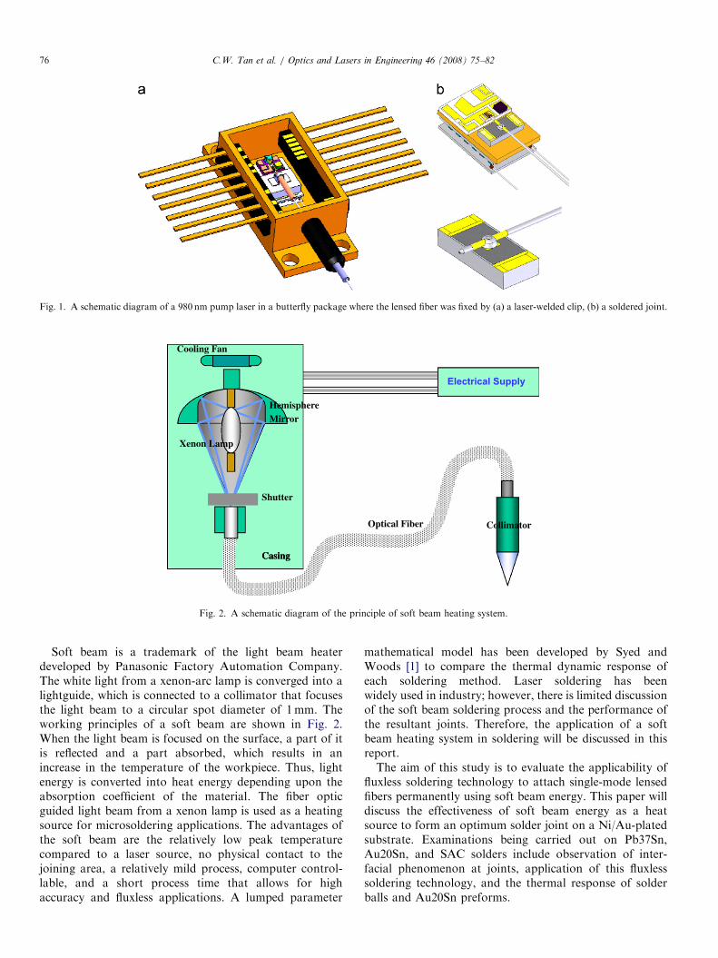
The most critical assembly process in packaging a laserdiode in a butterfly package is the lensed fiber to laserdiode alignment and affixing. Fig. 1 shows the schematicdiagrams of this lensed-fiber-affixing joint, which requiressub-micrometer accuracy for the maximum optical powercoupling efficiency. A laser-welding technique is the mostpopular method to permanently fix the lensed fiber that isattached in a metal ferrule onto the heat sink using a weldclip, as shown in Fig. 1a. Alternatively, focused lightenergy beams such as laser beams and soft beams havebeen increasingly employed to provide sufficient heatenergy to melt solder materials [1]. These soldered joints
e front matter r 2007 Elsevier Ltd. All rights reserved.
tlaseng.2007.06.007
ing author.
ess: [email protected] (Y.C. Chan).
that hold permanently metallized fibers to gold-platedsubstrates are shown in Fig. 1b.Soldering is a metallurgical joining technique in which the
molten solder spreads upon and chemically reacts with thesolder pad metallization. The optimum microstructure re-quired for a solder joint is a large-grained, finely dividedeutectic or near-eutectic structure [2,3]. This can be achievedby minimizing heat input and process time which causes rapidcooling during a soft beam soldering process. A bare substrate,KovarTM in this case, is not suited to direct soldering; thus, itis often electroplated with Au/Ni metallization to enhance itssolderability. The noble Au surface layer is critical to thesuccess of fluxless soldering where it prevents oxidation of theunderlying Ni layer before and during soldering. Fluxes areundesirable for this application because the flux residue mayflake-off and interfere with optical signals transmitted betweenthe fiber and the laser diode inside the package [4–7].
ARTICLE IN PRESS
Fig. 1. A schematic diagram of a 980 nm pump laser in a butterfly package where the lensed fiber was fixed by (a) a laser-welded clip, (b) a soldered joint.
Electrical Supply
Cooling Fan
Xenon Lamp
Shutter
HemisphereMirror
Casing
Optical Fiber
Casing
Collimator
Fig. 2. A schematic diagram of the principle of soft beam heating system.
C.W. Tan et al. / Optics and Lasers in Engineering 46 (2008) 75–8276
Soft beam is a trademark of the light beam heaterdeveloped by Panasonic Factory Automation Company.The white light from a xenon-arc lamp is converged into alightguide, which is connected to a collimator that focusesthe light beam to a circular spot diameter of 1mm. Theworking principles of a soft beam are shown in Fig. 2.When the light beam is focused on the surface, a part of itis reflected and a part absorbed, which results in anincrease in the temperature of the workpiece. Thus, lightenergy is converted into heat energy depending upon theabsorption coefficient of the material. The fiber opticguided light beam from a xenon lamp is used as a heatingsource for microsoldering applications. The advantages ofthe soft beam are the relatively low peak temperaturecompared to a laser source, no physical contact to thejoining area, a relatively mild process, computer control-lable, and a short process time that allows for highaccuracy and fluxless applications. A lumped parameter
mathematical model has been developed by Syed andWoods [1] to compare the thermal dynamic response ofeach soldering method. Laser soldering has beenwidely used in industry; however, there is limited discussionof the soft beam soldering process and the performance ofthe resultant joints. Therefore, the application of a softbeam heating system in soldering will be discussed in thisreport.The aim of this study is to evaluate the applicability of
fluxless soldering technology to attach single-mode lensedfibers permanently using soft beam energy. This paper willdiscuss the effectiveness of soft beam energy as a heatsource to form an optimum solder joint on a Ni/Au-platedsubstrate. Examinations being carried out on Pb37Sn,Au20Sn, and SAC solders include observation of inter-facial phenomenon at joints, application of this fluxlesssoldering technology, and the thermal response of solderballs and Au20Sn preforms.
ARTICLE IN PRESSC.W. Tan et al. / Optics and Lasers in Engineering 46 (2008) 75–82 77
2. Experimental methodology
In this joint configuration, the substrate is an Au/Ni-plated KovarTM heat sink. Pb37Sn solder balls with adiameter of 30 mm, SAC solder balls with a diameter of30 mm, and Au20Sn preform with a thickness of 30 mm wereused, to enable the control of the solder volume for eachtype of solder. A Panasonic YB02AC5 soft beam heatingsystem was used to prepare the soldered joints. As acomparison, a Unitek Miyachi LW52E Nd:YAG pulsedlaser source was used to simulate the extremely high peaktemperature and rapid cooling profile that accompaniesthis technique.
The temperature of the solder and the components mustbe monitored to ensure good solder quality. An OMEGA-ETTE HH306 Thermometer/Datalogger was used tomeasure the temperature profile at 1 s recording intervalsof various power and shutter open time settings as listed inTable 1. The focused white light was targeted on the Au/Nisubstrate and a thermocouple was attached to the substrateusing thermally conductive adhesive. The thermal signa-tures were obtained from the temperature–time diagrams,which indicate the minimum required conditions for goodjoints, maximum allowable thermal load of the compo-nents, and other process conditions.
Table 2 shows the parameters used to melt each soldertype. Based on the melting temperatures listed in Table 2,for a beam power giving a peak temperature lower thanthese, it is not possible to solder the solder ball onto thesubstrate without the application of flux. A Philips XL 40field emission gun (FEG) scanning electron microscopy(SEM) equipped with an X-ray energy-dispersive spectro-meter (EDX) was used to examine the microstructure andinterfacial phenomenon of the cross-sectioned solder joints.The chemical composition analysis was carried out by theEDX spectrometer (EDAX 10mm2 Si(Li) STUW detector)
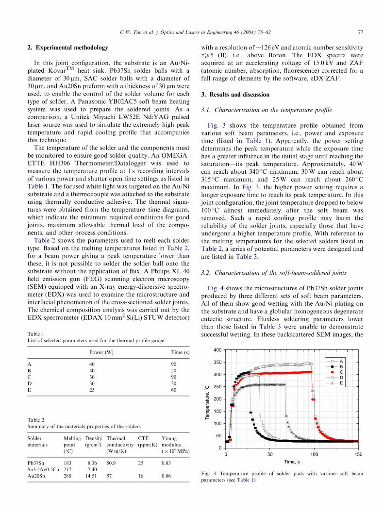
Table 1
List of selected parameters used for the thermal profile gauge
Power (W) Time (s)
A 40 90
B 40 20
C 30 90
D 30 30
E 25 60
Table 2
Summary of the materials properties of the solders
Solder
materials
Melting
point
(1C)
Density
(g/cm3)
Thermal
conductivity
(Wm/K)
CTE
(ppm/K)
Young
modulus
(� 106MPa)
Pb37Sn 183 8.36 50.9 25 0.03
Sn3.5Ag0.5Cu 217 7.40 – – –
Au20Sn 280 14.51 57 16 0.06
with a resolution of �126 eV and atomic number sensitivityzX5 (B), i.e., above Boron. The EDX spectra wereacquired at an accelerating voltage of 15.0 kV and ZAF(atomic number, absorption, fluorescence) corrected for afull range of elements by the software, eDX-ZAF.
3. Results and discussion
3.1. Characterization on the temperature profile
Fig. 3 shows the temperature profile obtained fromvarious soft beam parameters, i.e., power and exposuretime (listed in Table 1). Apparently, the power settingdetermines the peak temperature while the exposure timehas a greater influence in the initial stage until reaching thesaturation—its peak temperature. Approximately, 40Wcan reach about 340 1C maximum, 30W can reach about315 1C maximum, and 25W can reach about 260 1Cmaximum. In Fig. 3, the higher power setting requires alonger exposure time to reach its peak temperature. In thisjoint configuration, the joint temperature dropped to below100 1C almost immediately after the soft beam wasremoved. Such a rapid cooling profile may harm thereliability of the solder joints, especially those that haveundergone a higher temperature profile. With reference tothe melting temperatures for the selected solders listed inTable 2, a series of potential parameters were designed andare listed in Table 3.
3.2. Characterization of the soft-beam-soldered joints
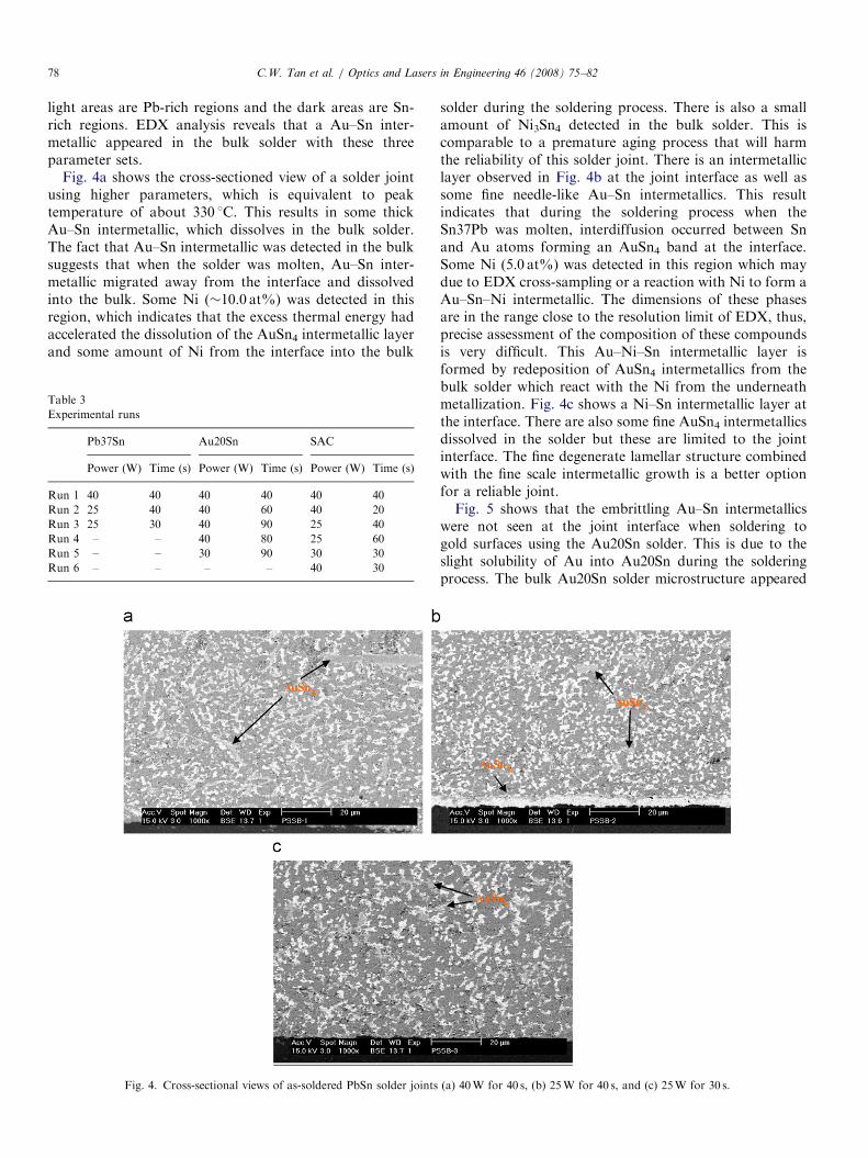
Fig. 4 shows the microstructures of Pb37Sn solder jointsproduced by three different sets of soft beam parameters.All of them show good wetting with the Au/Ni plating onthe substrate and have a globular homogeneous degenerateeutectic structure. Fluxless soldering parameters lowerthan those listed in Table 3 were unable to demonstratesuccessful wetting. In these backscattered SEM images, the
150100500
0
50
100
150
200
250
300
350
400
Te
mp
era
ture
, ° C
Time, s
A
B
C
D
E
Fig. 3. Temperature profile of solder pads with various soft beam
parameters (see Table 1).
ARTICLE IN PRESSC.W. Tan et al. / Optics and Lasers in Engineering 46 (2008) 75–8278
light areas are Pb-rich regions and the dark areas are Sn-rich regions. EDX analysis reveals that a Au–Sn inter-metallic appeared in the bulk solder with these threeparameter sets.
Fig. 4a shows the cross-sectioned view of a solder jointusing higher parameters, which is equivalent to peaktemperature of about 330 1C. This results in some thickAu–Sn intermetallic, which dissolves in the bulk solder.The fact that Au–Sn intermetallic was detected in the bulksuggests that when the solder was molten, Au–Sn inter-metallic migrated away from the interface and dissolvedinto the bulk. Some Ni (�10.0 at%) was detected in thisregion, which indicates that the excess thermal energy hadaccelerated the dissolution of the AuSn4 intermetallic layerand some amount of Ni from the interface into the bulk
Table 3
Experimental runs
Pb37Sn Au20Sn SAC
Power (W) Time (s) Power (W) Time (s) Power (W) Time (s)
Run 1 40 40 40 40 40 40
Run 2 25 40 40 60 40 20
Run 3 25 30 40 90 25 40
Run 4 – – 40 80 25 60
Run 5 – – 30 90 30 30
Run 6 – – – – 40 30
Fig. 4. Cross-sectional views of as-soldered PbSn solder joints
solder during the soldering process. There is also a smallamount of Ni3Sn4 detected in the bulk solder. This iscomparable to a premature aging process that will harmthe reliability of this solder joint. There is an intermetalliclayer observed in Fig. 4b at the joint interface as well assome fine needle-like Au–Sn intermetallics. This resultindicates that during the soldering process when theSn37Pb was molten, interdiffusion occurred between Snand Au atoms forming an AuSn4 band at the interface.Some Ni (5.0 at%) was detected in this region which maydue to EDX cross-sampling or a reaction with Ni to form aAu–Sn–Ni intermetallic. The dimensions of these phasesare in the range close to the resolution limit of EDX, thus,precise assessment of the composition of these compoundsis very difficult. This Au–Ni–Sn intermetallic layer isformed by redeposition of AuSn4 intermetallics from thebulk solder which react with the Ni from the underneathmetallization. Fig. 4c shows a Ni–Sn intermetallic layer atthe interface. There are also some fine AuSn4 intermetallicsdissolved in the solder but these are limited to the jointinterface. The fine degenerate lamellar structure combinedwith the fine scale intermetallic growth is a better optionfor a reliable joint.Fig. 5 shows that the embrittling Au–Sn intermetallics
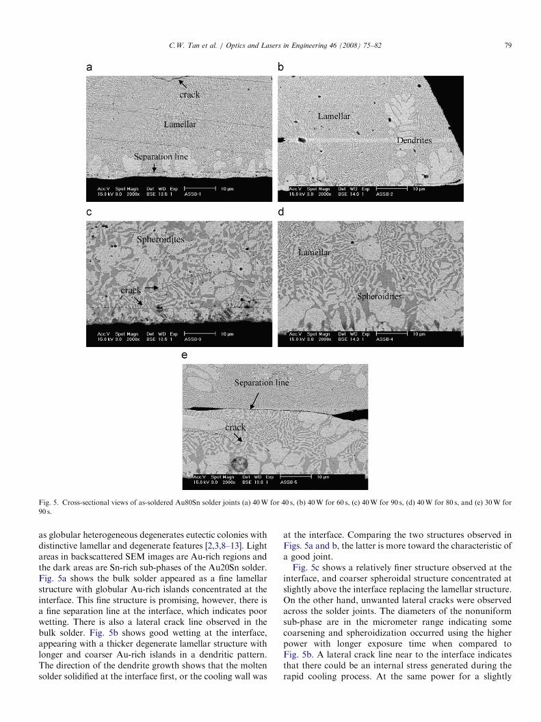
were not seen at the joint interface when soldering togold surfaces using the Au20Sn solder. This is due to theslight solubility of Au into Au20Sn during the solderingprocess. The bulk Au20Sn solder microstructure appeared
(a) 40W for 40 s, (b) 25W for 40 s, and (c) 25W for 30 s.
ARTICLE IN PRESS
Fig. 5. Cross-sectional views of as-soldered Au80Sn solder joints (a) 40W for 40 s, (b) 40W for 60 s, (c) 40W for 90 s, (d) 40W for 80 s, and (e) 30W for
90 s.
C.W. Tan et al. / Optics and Lasers in Engineering 46 (2008) 75–82 79
as globular heterogeneous degenerates eutectic colonies withdistinctive lamellar and degenerate features [2,3,8–13]. Lightareas in backscattered SEM images are Au-rich regions andthe dark areas are Sn-rich sub-phases of the Au20Sn solder.Fig. 5a shows the bulk solder appeared as a fine lamellarstructure with globular Au-rich islands concentrated at theinterface. This fine structure is promising, however, there isa fine separation line at the interface, which indicates poorwetting. There is also a lateral crack line observed in thebulk solder. Fig. 5b shows good wetting at the interface,appearing with a thicker degenerate lamellar structure withlonger and coarser Au-rich islands in a dendritic pattern.The direction of the dendrite growth shows that the moltensolder solidified at the interface first, or the cooling wall was
at the interface. Comparing the two structures observed inFigs. 5a and b, the latter is more toward the characteristic ofa good joint.Fig. 5c shows a relatively finer structure observed at the
interface, and coarser spheroidal structure concentrated atslightly above the interface replacing the lamellar structure.On the other hand, unwanted lateral cracks were observedacross the solder joints. The diameters of the nonuniformsub-phase are in the micrometer range indicating somecoarsening and spheroidization occurred using the higherpower with longer exposure time when compared toFig. 5b. A lateral crack line near to the interface indicatesthat there could be an internal stress generated during therapid cooling process. At the same power for a slightly
ARTICLE IN PRESSC.W. Tan et al. / Optics and Lasers in Engineering 46 (2008) 75–8280
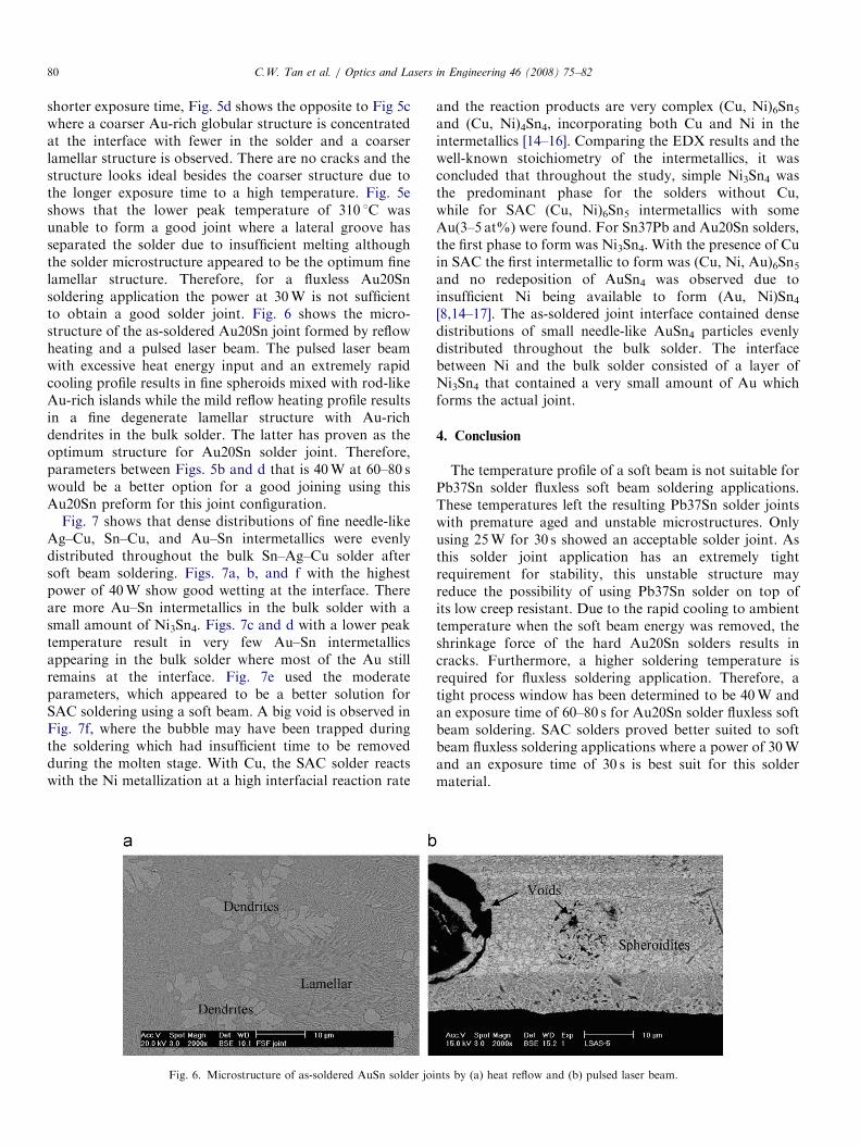
shorter exposure time, Fig. 5d shows the opposite to Fig 5cwhere a coarser Au-rich globular structure is concentratedat the interface with fewer in the solder and a coarserlamellar structure is observed. There are no cracks and thestructure looks ideal besides the coarser structure due tothe longer exposure time to a high temperature. Fig. 5eshows that the lower peak temperature of 310 1C wasunable to form a good joint where a lateral groove hasseparated the solder due to insufficient melting althoughthe solder microstructure appeared to be the optimum finelamellar structure. Therefore, for a fluxless Au20Snsoldering application the power at 30W is not sufficientto obtain a good solder joint. Fig. 6 shows the micro-structure of the as-soldered Au20Sn joint formed by reflowheating and a pulsed laser beam. The pulsed laser beamwith excessive heat energy input and an extremely rapidcooling profile results in fine spheroids mixed with rod-likeAu-rich islands while the mild reflow heating profile resultsin a fine degenerate lamellar structure with Au-richdendrites in the bulk solder. The latter has proven as theoptimum structure for Au20Sn solder joint. Therefore,parameters between Figs. 5b and d that is 40W at 60–80 swould be a better option for a good joining using thisAu20Sn preform for this joint configuration.
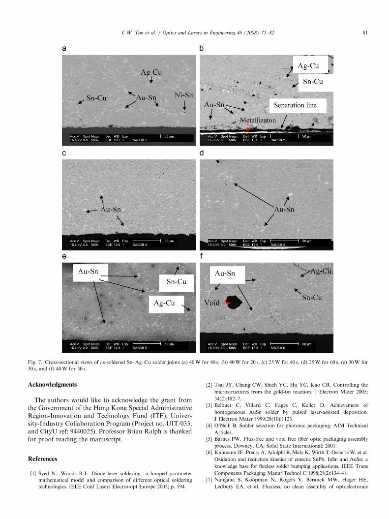
Fig. 7 shows that dense distributions of fine needle-likeAg–Cu, Sn–Cu, and Au–Sn intermetallics were evenlydistributed throughout the bulk Sn–Ag–Cu solder aftersoft beam soldering. Figs. 7a, b, and f with the highestpower of 40W show good wetting at the interface. Thereare more Au–Sn intermetallics in the bulk solder with asmall amount of Ni3Sn4. Figs. 7c and d with a lower peaktemperature result in very few Au–Sn intermetallicsappearing in the bulk solder where most of the Au stillremains at the interface. Fig. 7e used the moderateparameters, which appeared to be a better solution forSAC soldering using a soft beam. A big void is observed inFig. 7f, where the bubble may have been trapped duringthe soldering which had insufficient time to be removedduring the molten stage. With Cu, the SAC solder reactswith the Ni metallization at a high interfacial reaction rate
Fig. 6. Microstructure of as-soldered AuSn solder joi
and the reaction products are very complex (Cu, Ni)6Sn5and (Cu, Ni)4Sn4, incorporating both Cu and Ni in theintermetallics [14–16]. Comparing the EDX results and thewell-known stoichiometry of the intermetallics, it wasconcluded that throughout the study, simple Ni3Sn4 wasthe predominant phase for the solders without Cu,while for SAC (Cu, Ni)6Sn5 intermetallics with someAu(3–5 at%) were found. For Sn37Pb and Au20Sn solders,the first phase to form was Ni3Sn4. With the presence of Cuin SAC the first intermetallic to form was (Cu, Ni, Au)6Sn5and no redeposition of AuSn4 was observed due toinsufficient Ni being available to form (Au, Ni)Sn4[8,14–17]. The as-soldered joint interface contained densedistributions of small needle-like AuSn4 particles evenlydistributed throughout the bulk solder. The interfacebetween Ni and the bulk solder consisted of a layer ofNi3Sn4 that contained a very small amount of Au whichforms the actual joint.
4. Conclusion
The temperature profile of a soft beam is not suitable forPb37Sn solder fluxless soft beam soldering applications.These temperatures left the resulting Pb37Sn solder jointswith premature aged and unstable microstructures. Onlyusing 25W for 30 s showed an acceptable solder joint. Asthis solder joint application has an extremely tightrequirement for stability, this unstable structure mayreduce the possibility of using Pb37Sn solder on top ofits low creep resistant. Due to the rapid cooling to ambienttemperature when the soft beam energy was removed, theshrinkage force of the hard Au20Sn solders results incracks. Furthermore, a higher soldering temperature isrequired for fluxless soldering application. Therefore, atight process window has been determined to be 40W andan exposure time of 60–80 s for Au20Sn solder fluxless softbeam soldering. SAC solders proved better suited to softbeam fluxless soldering applications where a power of 30Wand an exposure time of 30 s is best suit for this soldermaterial.
nts by (a) heat reflow and (b) pulsed laser beam.
ARTICLE IN PRESS
Fig. 7. Cross-sectional views of as-soldered Sn–Ag–Cu solder joints (a) 40W for 40 s, (b) 40W for 20 s, (c) 25W for 40 s, (d) 25W for 60 s, (e) 30W for
30 s, and (f) 40W for 30 s.
C.W. Tan et al. / Optics and Lasers in Engineering 46 (2008) 75–82 81
Acknowledgments
The authors would like to acknowledge the grant fromthe Government of the Hong Kong Special AdministrativeRegion-Innovation and Technology Fund (ITF), Univer-sity-Industry Collaboration Program (Project no. UIT/033,and CityU ref: 9440025). Professor Brian Ralph is thankedfor proof reading the manuscript.
References
[1] Syed N., Woods R.L. Diode laser soldering—a lumped parameter
mathematical model and comparison of different optical soldering
technologies. IEEE Conf Lasers Electro-opt Europe 2003; p. 594.
[2] Tsai JY, Chang CW, Shieh YC, Hu YC, Kao CR. Controlling the
microstructures from the gold-tin reaction. J Electron Mater 2005;
34(2):182–7.
[3] Belouet C, Villard C, Fages C, Keller D. Achievement of
homogeneous AuSn solder by pulsed laser-assisted deposition.
J Electron Mater 1999;28(10):1123.
[4] O’Neill B. Solder selection for photonic packaging. AIM Technical
Articles.
[5] Barnes PW. Flux-free and void free fiber optic packaging assembly
process. Downey, CA: Solid State International; 2001.
[6] Kuhmann JF, Preuss A, Adolphi B, Maly K, Wirth T, Oesterle W, et al.
Oxidation and reduction kinetics of eutectic SnPb, InSn and AuSn: a
knowledge base for fluxless solder bumping applications. IEEE Trans
Components Packaging Manuf Technol C 1998;21(2):134–41.
[7] Nangalia S, Koopman N, Rogers V, Beranek MW, Hager HE,
Ledbury EA, et al. Fluxless, no clean assembly of optoelectronic
ARTICLE IN PRESSC.W. Tan et al. / Optics and Lasers in Engineering 46 (2008) 75–8282
devices with PADS. In: Proceedings of the IEEE electronic
components and technology conference, 1997. p. 755–62.
[8] Lee JH, Park JW, Shin DH, Kim YS. Kinetics of the Au–Ni–Sn
ternary intermetallic layer redeposition at the solder/under-bump
metallurgy interface during aging treatment. J Electron Mater
2004;33(1):28–33.
[9] Ivey DG. Microstructural characterization of Au/Sn solder for
packaging in optoelectronic applications. Micron 1998;29(4):281–7.
[10] Yamada T, Miura K, Kajihara M, Kurokawa N, Sakamoto K.
Kinetics of reactive diffusion between Au and Sn during annealing at
solid-state temperatures. Mater Sci Eng, A 2005;390:118–26.
[11] Anhock S, Oppermann H, Kallmayer C, Aschenbrenner R, Thomas
L, Reichl H. Investigations of Au/Sn alloys on different end-
metallizations for high temperature applications. In: Proceedings of
IEEE/CPMT Int’l electronic manufacturing technology symposium,
Berlin, German, 1998. p. 156–64.
[12] Beranek MW, Rassaian M, Tang CH, St. John CL, Loebs VA.
Characterization of 63Sn37Pb and 80Au20Sn solder sealed optical
fiber feedthroughs subjected to repetitive thermal cycling. IEEE
Trans Adv Packaging 2001;24(4):576–85.
[13] Kuang JH, Sheen MT, Chang CFH, Chen CC, Wang GL, Cheng
WH. Effect of temperature cycling on joint strength of PbSn and
AuSn solders in laser packages. IEEE Trans Adv Packaging
2001;24(4):563–8.
[14] Alam MO, Chan YC, Tu KN, Kivilahti JK. Effect of 0.5wt%Cu in
Sn-3.5%Ag solder balls on the solid state interfacial reaction with
Au/Ni/Cu bond pads for ball grid array (BGA) applications. Chem
Mater Commun 2005;17(9):2223–6.
[15] Islam MN, Chan YC. Interfacial reactions of Cu-containing lead-free
solders with Au/NiP metallization. J Electron Mater 2005;34(5):662–9.
[16] Laurila T, Vuorinen V, Mattila T, Kivilahti JK. Analysis of the
redeposition of AuSn4 on Ni/Au contact pads when using SnPbAg,
SnAg and SnAgCu solders. J Electron Mater 2005;34(1):103–11.
[17] Mita M, Miura K, Takenaka T, Kajihara M, Kurokawa N,
Sakamoto K. Effect of Ni on reactive diffusion between Au and Sn
at solid-state temperatures. Mater Sci Eng, B 2006;126(1):37–43.