Effectiveness of PCB Perimeter Via Fencing - NDSUbraaten/EMC_2016_1.pdf · The PCB design was...
6
Effectiveness of PCB Perimeter Via Fencing Radially Propagating EMC Emissions Reduction Technique Waylon Lindseth North Dakota State University, Electrical Engineering Department Student John Deere Electronic Solutions, Electrical Engineer Fargo, ND, USA [email protected] Abstract – Via fencing around the periphery of a printed circuit board is a practice to attempt to eliminate radially propagated energy from the edge of a board. This study comparatively analyzed via fenced boards against unfenced boards as well as investigated other emission related design variables including trace distance from the PCB edge, termination loads, and via fence spacing. The S 21 measurements were taken with a network analyzer and a horn antenna with the PCB trace as the source. Frequency sweeps from 1-8.5GHz showed that via fencing attenuated as much as 21dB at some frequencies, concluding that via fencing was definitively beneficial. Trace distances to the edge of the board showed mixed results at lower frequencies, but gave higher emissions with smaller distances to the edge at higher frequencies. Varying loads yielded results showing emissions for given loads were highly dependent on frequency with the exception of the dominant short-circuit load. Via fence spacing was shown to be significant, but only loosely followed the 1/8 th wavelength rule of thumb. This study proved to be very important for the electronics industry as EMC regulations are increasingly harder to meet with shrinking die process technologies and rising clock frequencies. Keywords – Printed circuit board, via fencing, radial propagating emissions. I. INTRODUCTION One of the dominant mechanisms [1] of emissions is radially propagated electromagnetic waves excited by currents through vias and traces which are funneled by pseudo-waveguides by the top and bottom layer ground and/or power planes. Most of the energy is transmitted into air from the PCB’s edge causing EMC radiated emissions as shown in Fig. 1. The frequencies of the radiated energy are dependent on the via heights (PCB thickness) and trace lengths, and amplitudes change with the distance through the dielectric and its properties. Other variables, such as substrates (dielectrics), will not be examined in this study. To combat this problem some designers have used the 20-H Rule which is a practice of recessing one plane by a distance of twenty times the distance between the two parallel planes. This practice has been studied and shown to only minimally reduce emissions [2] and in some cases, such as a 2 layer stack-up, the emissions were increased [3] due to the recessed plane allowing the opposite plane to become a patch antenna – transferring the emissions from the X and Y axis to the Z axis. Fig. 1. Sources including (1) vias and (2) internal asymmetric stripline traces. Ground planes are effective waveguide for (3) incident wave and the (4) transmitted wave. Fig. 2. Cross-sectional view of the via fencing theory: Sources including (1) vias and (2) internal asymmetric stripline trace and ground planes as waveguide for (3) incident wave as before, but (4) ground stitching vias creates an impedance boundary that (5) reflects the wave internally. This also removes valuable layout real estate which makes the practice inefficient and ineffective. One concept that is more practical in current designs is utilizing impedance boundaries as an advantage, illustrated by Figure 2. The goal of minimizing transmitted energy is achieved by maximizing reflected energy. A normal PCB provides what is effectively an infinite (open) impedance boundary. Knowing that with open impedance boundaries energy can be measured coming from the edge of the PCB, other impedance boundary values should be investigated. The top and bottom ground planes in the Z direction and the perimeter ground terminations in the X and Y directions create a three dimensional zero-impedance boundary. This theoretically keeps the energy internal to the PCB structure since it is reflected from the perimeter keeping it from being emitted. This can be done with edge plating or via fencing, but edge plating has many negative side-effects [4] including the need for unmasked copper bands around the perimeter of both planes for the plating to connect to, the inability for 100% coverage due to handling needs during manufacturing, and only selective chemical nickel-gold finishes suitable as choices. 978-1-5090-1442-2/16/$31.00 ©2016 IEEE 627
Transcript of Effectiveness of PCB Perimeter Via Fencing - NDSUbraaten/EMC_2016_1.pdf · The PCB design was...

Effectiveness of PCB Perimeter Via FencingRadially Propagating EMC Emissions Reduction Technique
Waylon LindsethNorth Dakota State University, Electrical Engineering Department Student
John Deere Electronic Solutions, Electrical EngineerFargo, ND, USA
Abstract – Via fencing around the periphery of a printed circuitboard is a practice to attempt to eliminate radially propagatedenergy from the edge of a board. This study comparativelyanalyzed via fenced boards against unfenced boards as well asinvestigated other emission related design variables includingtrace distance from the PCB edge, termination loads, and viafence spacing. The S21 measurements were taken with a networkanalyzer and a horn antenna with the PCB trace as the source.Frequency sweeps from 1-8.5GHz showed that via fencingattenuated as much as 21dB at some frequencies, concluding thatvia fencing was definitively beneficial. Trace distances to the edgeof the board showed mixed results at lower frequencies, but gavehigher emissions with smaller distances to the edge at higherfrequencies. Varying loads yielded results showing emissions forgiven loads were highly dependent on frequency with theexception of the dominant short-circuit load. Via fence spacingwas shown to be significant, but only loosely followed the 1/8th
wavelength rule of thumb. This study proved to be veryimportant for the electronics industry as EMC regulations areincreasingly harder to meet with shrinking die processtechnologies and rising clock frequencies.
Keywords – Printed circuit board, via fencing, radialpropagating emissions.
I. INTRODUCTION
One of the dominant mechanisms [1] of emissions is radiallypropagated electromagnetic waves excited by currents throughvias and traces which are funneled by pseudo-waveguides bythe top and bottom layer ground and/or power planes. Most ofthe energy is transmitted into air from the PCB’s edge causingEMC radiated emissions as shown in Fig. 1. The frequencies ofthe radiated energy are dependent on the via heights (PCBthickness) and trace lengths, and amplitudes change with thedistance through the dielectric and its properties. Othervariables, such as substrates (dielectrics), will not be examinedin this study.
To combat this problem some designers have used the 20-HRule which is a practice of recessing one plane by a distance oftwenty times the distance between the two parallel planes. Thispractice has been studied and shown to only minimally reduceemissions [2] and in some cases, such as a 2 layer stack-up, theemissions were increased [3] due to the recessed planeallowing the opposite plane to become a patch antenna –transferring the emissions from the X and Y axis to the Z axis.
Fig. 1. Sources including (1) vias and (2) internal asymmetric stripline traces.Ground planes are effective waveguide for (3) incident wave and the (4)
transmitted wave.
Fig. 2. Cross-sectional view of the via fencing theory: Sources including (1)vias and (2) internal asymmetric stripline trace and ground planes as
waveguide for (3) incident wave as before, but (4) ground stitching viascreates an impedance boundary that (5) reflects the wave internally.
This also removes valuable layout real estate which makes thepractice inefficient and ineffective.
One concept that is more practical in current designs isutilizing impedance boundaries as an advantage, illustrated byFigure 2. The goal of minimizing transmitted energy isachieved by maximizing reflected energy. A normal PCBprovides what is effectively an infinite (open) impedanceboundary. Knowing that with open impedance boundariesenergy can be measured coming from the edge of the PCB,other impedance boundary values should be investigated.
The top and bottom ground planes in the Z direction andthe perimeter ground terminations in the X and Y directionscreate a three dimensional zero-impedance boundary. Thistheoretically keeps the energy internal to the PCB structuresince it is reflected from the perimeter keeping it from beingemitted. This can be done with edge plating or via fencing, butedge plating has many negative side-effects [4] including theneed for unmasked copper bands around the perimeter of bothplanes for the plating to connect to, the inability for 100%coverage due to handling needs during manufacturing, andonly selective chemical nickel-gold finishes suitable as choices.
978-1-5090-1442-2/16/$31.00 ©2016 IEEE 627

There have been multiple studies and reports about thegeneral subject of via fencing but their work is limited toanalyzing the via itself as the source of radiation [1] and viafencing being used to minimize crosstalk [5] between signalsinternal to the design.
The rule of thumb that a stub starts to become reactive as itapproached 1/8th of a wavelength has been known and followedsince the early 70’s [5]. This same principle shows that thespace between vias also starts to look reactive as the spacingapproaches 1/8th of a wavelength. That supposedly means thatif the spacing between ground fencing vias is less than 1/8th ofa wavelength, via fencing should appear to be the same as asolid ground impedance barrier. To utilize the 1/8th wavelengthprinciple for this study, the well-known frequency-to-wavelength equation was altered slightly to reflect the 1/8th
wavelength as shown in Eq. 1.
The relationship of frequency to wavelength – and with Eq.1 also via fencing – is shown in Table I. According to this 1/8th
wavelength rule, for an emission regulation ceiling of 2 GHz,via spacing of about 375 mils should be enough to suppress theradiation of any frequencies of interest.
TABLE I. RELATION BETWEEN WAVELENGTH AND VIA SPACING
Spacing (mils) λ (in) Frequency (GHz)
25 0.20 30.274
50 0.40 15.137
100 0.80 7.568
150 1.20 5.046
200 1.60 3.784
300 2.40 2.523
500 4.00 1.514
1000 8.00 0.757
This study was intended to determine whether perimeter viafencing for reducing EMC emissions is effective whencompared to adequate ground paths through vias for sub-10GHz frequencies. To expand on this subject, this paper willalso address other potential questions regarding via fencing andPCB design. While identifying the variables involved thatmight have effect on radially propagating emissions, it wasdiscovered that this study could address multiple aspects ofPCB design. The derived secondary purposes of the studyencompassed the effects of parallel distance from a signal traceto the edge of the board, varying termination loads, and if the1/8th wavelength rule of thumb correctly estimates via fencingspacing.
Fig. 3. Expanded view of the study’s PCB design and antenna: (1) Top andbottom conductor layers as ground planes. (2) Vias used to connect trace
antenna to load/coaxial header. (3) Internal conductor layer 3 with atrace used as an antenna. (4) Notice conductor layer 2 is missing.
II. METHODS
Prototype FabricationThe PCB design was intended to emulate industry
electronic design practices as closely as possible to make thevalue higher for current electronic and PCB design. For thisreason FR408 material was chosen as the dielectric materialand 1 ounce copper layers with silver finish. The board outlinewas chosen to be 4 inches by 4 inches due to panelizingreasons and to increase the ease of handling. All vias were acommon 15 mil drill hole with 1 mil plating.
A 3 layer PCB was designed using the external conductivelayers used as the ground planes and a single trace on theinternal layer serves as the sourcing antenna as shown in Figure3. This resulting asymmetric stack-up was chosen to emulatenormal 4-layer PCB manufacturing practices.
The antenna length was chosen to be 2.15 inches, being anapproximate resonant length for 5.49 GHz, which is at the highend for DDR DQ and other high speed transmission lineslengths and well within the 1-8.5 GHz capability of the VNAused for this study.
. Using a Saturn PCB Design Tool [7], the trace width toobtain 50Ω characteristic impedance was 13 mils when usingthe asymmetrical stripline parameters and the FR408 relativepermittivity of 3.8. A standard 62 mil board thickness meantthe height from the layer 3 trace to the bottom layer is 9.45mils, and the distance from the top conductive layer is 49 mils.
To make sure the different designs can be objectivelycompared, both the fenced and the unfenced boards weredesigned to have identical numbers of vias. This, in theory,created the same number of paths to ground and avoidedcontamination of the study by eliminating any unwantedvariables. For a similar reason, all eight of the PCB designswere made into one panel to avoid any potential platingdifferences between fabrication runs.
Study Variables AddressedTo address the study’s first and main facet of whether via
fencing helps when compared to unfenced boards, there weretwo major layout topologies. Four of the boards had perimetervia fencing and four had vias only on the two sides that areperpendicular to the trace antenna and have no bearing on the
628
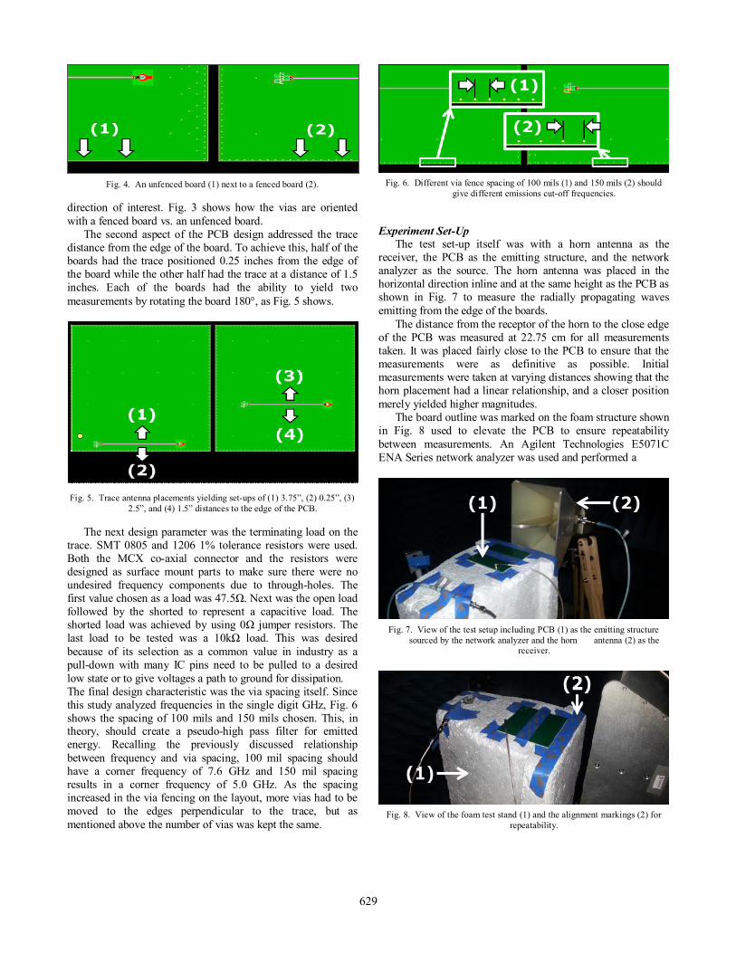
Fig. 4. An unfenced board (1) next to a fenced board (2).
direction of interest. Fig. 3 shows how the vias are orientedwith a fenced board vs. an unfenced board.
The second aspect of the PCB design addressed the tracedistance from the edge of the board. To achieve this, half of theboards had the trace positioned 0.25 inches from the edge ofthe board while the other half had the trace at a distance of 1.5inches. Each of the boards had the ability to yield twomeasurements by rotating the board 180°, as Fig. 5 shows.
Fig. 5. Trace antenna placements yielding set-ups of (1) 3.75”, (2) 0.25”, (3)2.5”, and (4) 1.5” distances to the edge of the PCB.
The next design parameter was the terminating load on thetrace. SMT 0805 and 1206 1% tolerance resistors were used.Both the MCX co-axial connector and the resistors weredesigned as surface mount parts to make sure there were noundesired frequency components due to through-holes. Thefirst value chosen as a load was 47.5Ω. Next was the open loadfollowed by the shorted to represent a capacitive load. Theshorted load was achieved by using 0Ω jumper resistors. Thelast load to be tested was a 10kΩ load. This was desiredbecause of its selection as a common value in industry as apull-down with many IC pins need to be pulled to a desiredlow state or to give voltages a path to ground for dissipation.The final design characteristic was the via spacing itself. Sincethis study analyzed frequencies in the single digit GHz, Fig. 6shows the spacing of 100 mils and 150 mils chosen. This, intheory, should create a pseudo-high pass filter for emittedenergy. Recalling the previously discussed relationshipbetween frequency and via spacing, 100 mil spacing shouldhave a corner frequency of 7.6 GHz and 150 mil spacingresults in a corner frequency of 5.0 GHz. As the spacingincreased in the via fencing on the layout, more vias had to bemoved to the edges perpendicular to the trace, but asmentioned above the number of vias was kept the same.
Fig. 6. Different via fence spacing of 100 mils (1) and 150 mils (2) shouldgive different emissions cut-off frequencies.
Experiment Set-UpThe test set-up itself was with a horn antenna as the
receiver, the PCB as the emitting structure, and the networkanalyzer as the source. The horn antenna was placed in thehorizontal direction inline and at the same height as the PCB asshown in Fig. 7 to measure the radially propagating wavesemitting from the edge of the boards.
The distance from the receptor of the horn to the close edgeof the PCB was measured at 22.75 cm for all measurementstaken. It was placed fairly close to the PCB to ensure that themeasurements were as definitive as possible. Initialmeasurements were taken at varying distances showing that thehorn placement had a linear relationship, and a closer positionmerely yielded higher magnitudes.
The board outline was marked on the foam structure shownin Fig. 8 used to elevate the PCB to ensure repeatabilitybetween measurements. An Agilent Technologies E5071CENA Series network analyzer was used and performed a
Fig. 7. View of the test setup including PCB (1) as the emitting structuresourced by the network analyzer and the horn antenna (2) as the
receiver.
Fig. 8. View of the foam test stand (1) and the alignment markings (2) forrepeatability.
629
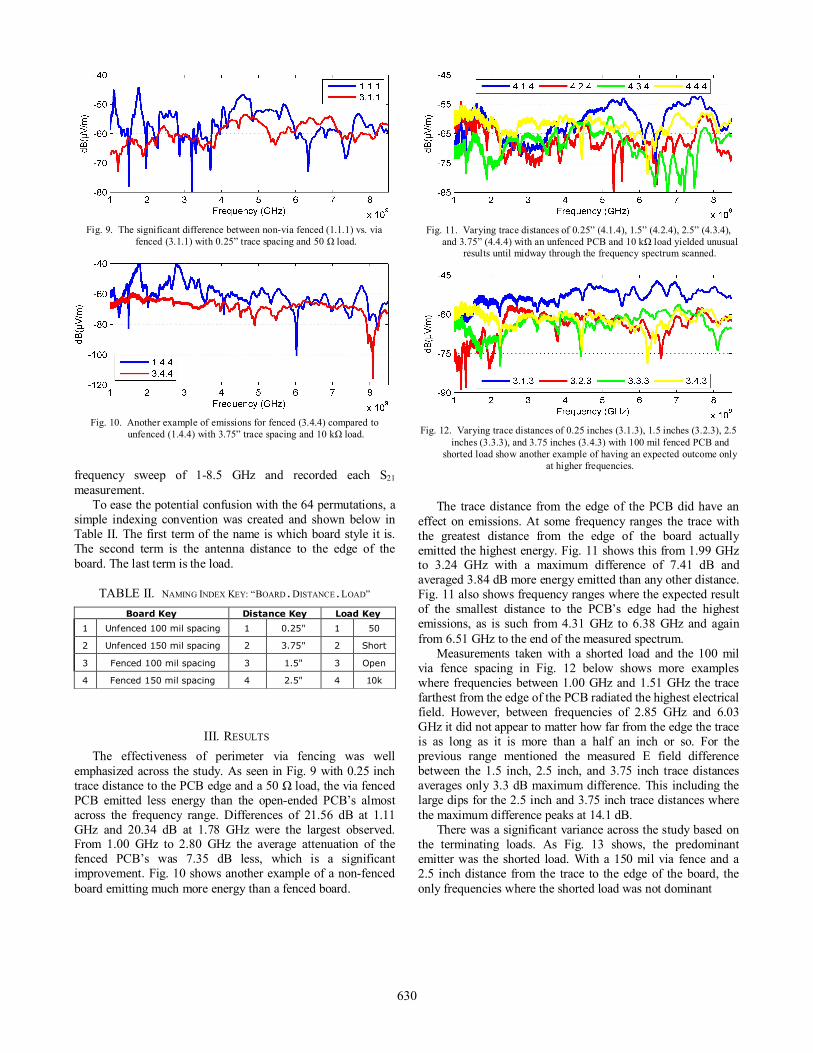
Fig. 9. The significant difference between non-via fenced (1.1.1) vs. viafenced (3.1.1) with 0.25” trace spacing and 50 Ω load.
Fig. 10. Another example of emissions for fenced (3.4.4) compared tounfenced (1.4.4) with 3.75” trace spacing and 10 kΩ load.
frequency sweep of 1-8.5 GHz and recorded each S21measurement.
To ease the potential confusion with the 64 permutations, asimple indexing convention was created and shown below inTable II. The first term of the name is which board style it is.The second term is the antenna distance to the edge of theboard. The last term is the load.
TABLE II. NAMING INDEX KEY: “BOARD . DISTANCE . LOAD”
Board Key Distance Key Load Key1 Unfenced 100 mil spacing 1 0.25" 1 50
2 Unfenced 150 mil spacing 2 3.75" 2 Short
3 Fenced 100 mil spacing 3 1.5" 3 Open
4 Fenced 150 mil spacing 4 2.5" 4 10k
III. RESULTS
The effectiveness of perimeter via fencing was wellemphasized across the study. As seen in Fig. 9 with 0.25 inchtrace distance to the PCB edge and a 50 Ω load, the via fencedPCB emitted less energy than the open-ended PCB’s almostacross the frequency range. Differences of 21.56 dB at 1.11GHz and 20.34 dB at 1.78 GHz were the largest observed.From 1.00 GHz to 2.80 GHz the average attenuation of thefenced PCB’s was 7.35 dB less, which is a significantimprovement. Fig. 10 shows another example of a non-fencedboard emitting much more energy than a fenced board.
Fig. 11. Varying trace distances of 0.25” (4.1.4), 1.5” (4.2.4), 2.5” (4.3.4),and 3.75” (4.4.4) with an unfenced PCB and 10 kΩ load yielded unusual
results until midway through the frequency spectrum scanned.
Fig. 12. Varying trace distances of 0.25 inches (3.1.3), 1.5 inches (3.2.3), 2.5inches (3.3.3), and 3.75 inches (3.4.3) with 100 mil fenced PCB and
shorted load show another example of having an expected outcome onlyat higher frequencies.
The trace distance from the edge of the PCB did have aneffect on emissions. At some frequency ranges the trace withthe greatest distance from the edge of the board actuallyemitted the highest energy. Fig. 11 shows this from 1.99 GHzto 3.24 GHz with a maximum difference of 7.41 dB andaveraged 3.84 dB more energy emitted than any other distance.Fig. 11 also shows frequency ranges where the expected resultof the smallest distance to the PCB’s edge had the highestemissions, as is such from 4.31 GHz to 6.38 GHz and againfrom 6.51 GHz to the end of the measured spectrum.
Measurements taken with a shorted load and the 100 milvia fence spacing in Fig. 12 below shows more exampleswhere frequencies between 1.00 GHz and 1.51 GHz the tracefarthest from the edge of the PCB radiated the highest electricalfield. However, between frequencies of 2.85 GHz and 6.03GHz it did not appear to matter how far from the edge the traceis as long as it is more than a half an inch or so. For theprevious range mentioned the measured E field differencebetween the 1.5 inch, 2.5 inch, and 3.75 inch trace distancesaverages only 3.3 dB maximum difference. This including thelarge dips for the 2.5 inch and 3.75 inch trace distances wherethe maximum difference peaks at 14.1 dB. There was a significant variance across the study based onthe terminating loads. As Fig. 13 shows, the predominantemitter was the shorted load. With a 150 mil via fence and a2.5 inch distance from the trace to the edge of the board, theonly frequencies where the shorted load was not dominant
630

Fig. 13. Varying loads of 50Ω (4.3.1), open (4.3.2), short (4.3.3), and 10kΩ(4.3.4) with a 150 mil fenced board and 2.5” trace distance.
Fig. 14. Resistive load compare of 50 Ω (blue) and 10 kΩ (red) terminationswith a 150 mil fenced board and 1.5” trace distance.
were the small frequency ranges of 1.48 GHz to 2.00 GHz,from 4.51 GHz to 4.72 GHz, and again from 5.06 GHz to5.31GHz. The open load had a maximum margin of 17.23 dBat 6.98 GHz which is a very high difference. It was noted thatthe 50 Ω load did not have the least emissions across the testedspectrum as hypothesized. It was the lowest for certain rangesas shown from 1.24 GHz to 2.66 GHz and again from 3.70GHz to 5.33 GHz with the exception of the two valleys thatbriefly intersect; the shorted load at 4.03 GHz and the openload at 4.65 GHz.
There was a switching of dominance of emissions betweenthe 50 Ω load and the 10 kΩ loads when directly compared inFig. 14. From 1.00 GHz to 2.22 GHz the 10 kΩ load emittedon average 8.31 dB more than the 50 Ω load; which is whatwas hypothesized. Unexpectedly, the two cross and exchangeplaces and up to 3.53 GHz the 50 Ω load emits on average 6.55dB more. For the rest of the frequencies the 10 kΩ load edgesthe 50 Ω load for emissions by a small 1.54 dB margin onaverage, but with difference as high as 26.73 dB at 7.06 GHz.
The results for varying via spacing in Fig. 15 showed the100 mil spaced fencing and the 150 mil spaced fencingmeasurements were virtual copies of each other until the 4.20GHz mark, where up to that point they averaged a difference ofonly 1.36 dB. After around 4.6 GHz the emissions for the twofenced boards are continuously dissimilar from each other. The150 mil spaced board had a calculated corner frequency of 5.05GHz, but even beyond 7 GHz the unfenced board and the 150mil fenced boards measure quite different magnitudes. The oneexception is from 7.58 GHz to 7.71 GHz where the measuredvalues of all three boards were within 5 dB.
Fig. 15. The 1/8th wavelength rule was tested by comparing the unfenced(1.4.1) against 100 mil spaced (3.4.1) and 150 mil spaced via fencing
(4.4.1) with 3.75” trace distance and 50 Ω load configuration.
IV. DISCUSSION
The effectiveness of perimeter via fencing for radiallypropagating emissions was evident in the study. The benefit ofvia fenced PCB’s when compared to the unfenced PCB’s withrespect to emissions was reinforced in every direct comparativemeasurement at a majority of frequencies, albeit not uniformlyacross all frequencies and configurations. A secondaryobservation when measuring via fenced boards was thatfencing seemed to stabilize the peaks and valleys in someplaces, however again, not across all frequencies andconfigurations. The measurements on fenced boards had muchsmaller ∆dB and lessened the more drastic slopes and changesof electric field magnitudes across frequencies than the open-ended boards.
The trace distance from the edge of the PCB did have aneffect on emissions, but not consistently in the wayhypothesized in the introduction of this study. There was anunexpected result of the trace farthest from the board edgeemitted more than any other trace at some lower frequencies,but for the most part the trace spaced only a quarter of an inchfrom the edge dominated the emissions as expected. Thesemixed results means that a design rule for whether or not viafencing should be used cannot be based on trace distance fromthe edge of the PCB alone.
Varying loads yielded different results for emissions. Atspecific frequencies the difference in magnitude was negligiblefor all load/trace distance/board style configurations, but insome cases it mattered greatly. The short circuit had the highestemissions over most of the frequency ranges which is whatmany capacitive loads would look like at these higherfrequencies. The open circuit load emulated something like atest point and had the least emissions about half the time. Whenthe 50Ω load was directly compared to the 10kΩ load therewas a switching of dominance between 1GHz to 3.5GHz that isattributed to the internal resonance due to the PCB dimensions.This goes to show – like the varying trace distance compare – adesign rule for whether or not via fencing should be usedcannot be based on what termination load is used alone.
Spacing between the vias of perimeter fencing did have asmall amount of influence on the measured emissions, but for
631
this study the results were less than conclusive. Neither of thetwo boards emulated the reference unfenced board andcontinued to attenuate emissions well past the calculatedfrequency using the 1/8th wavelength rule. The plots did seemto converge relative to the unfenced board, but there wasenough difference to doubt the effectiveness of the 1/8th
wavelength rule of thumb for via spacing.This study used very carefully controlled variables in a
minimally populated board and layout. It should be noted that afull electronics design will have multiple sources with multipleloads and a vast difference in trace distances from the edges ofthe board.
A real-world design will also have a number of vias alreadyin the design by necessity. Via fencing will add to the numberin the design, not just be repositioned. Additional vias are notusually an adder for unit cost as the set-up is what is timeconsuming. Going from 1,000 vias to 2,000 will only add acouple pennies on even moderately low annual unit volumes.
Via fencing as a practice could have some potentialnegative side-effects to signal integrity since the energy doeshave to couple to something. There could also be some concernto introducing some internal resonance issues, and both ofthese concerns should be noted when attempting to put viafencing into practice for PCB design.
There are also some possible ramifications to perimetervias for manufacturing purposes, such as potential foraccidental grounding of a metal enclosure. This would cause alack of case isolation – and creating a possible antenna for avehicle level EMC emission source – if a unit is so designed.
ACKNOWLEDGMENT
The author would like to thank Ryan King, Brian Booth,Dave Gira, and Will Cooper for their assistance in the study.An additional thank you is directed to John Deere ElectronicSolutions for the funding of the study.
REFERENCES
[1] F. Gisin, Z. Pantic-Tanner, “Minimizing EMI Caused byRadially Propagating Waves Inside High Speed Digital LogicPCBs”.
[2] H. Chen. "Effects of 20-H Rule and Shielding Vias onElectromagnetic Radiation From Printed Circuit Boards"
[3] M. Montrose, L. Enxiao, E-P. Li, “Analysis on the Effectivenessof Printed Circuit Board Edge Termination Using DiscreteComponents Instead of Implementing the 20-H Rule”.
[4] D. Stans, “Copper and the board edge”, Euro Circuits PCBDesign & Layout Guide
[5] A. Suntives, A. Khajoocizadeh, R. Abhari, “Using Via Fencingfor Crosstalk Reduction in PCB Circuits”.
[6] S. Hageman, “Via Spacing on High-performance PCB’s”.[7] Saturn PCB Design Toolkit Version 6.86, Saturn PCB Design
Inc. site.
632