Effect of stress migration on electromigration for nano ...
225
This document is downloaded from DR‑NTU (https://dr.ntu.edu.sg) Nanyang Technological University, Singapore. Effect of stress migration on electromigration for nano scale advanced interconnects Anson Heryanto 2012 Anson, Heryanto. (2012). Effect of stress migration on electromigration for nano scale advanced interconnects. Doctoral thesis, Nanyang Technological University, Singapore. https://hdl.handle.net/10356/50271 https://doi.org/10.32657/10356/50271 Downloaded on 24 Feb 2022 06:49:03 SGT
Transcript of Effect of stress migration on electromigration for nano ...

This document is downloaded from DR‑NTU (https://dr.ntu.edu.sg)Nanyang Technological University, Singapore.
Effect of stress migration on electromigration fornano scale advanced interconnects
Anson Heryanto
2012
Anson, Heryanto. (2012). Effect of stress migration on electromigration for nano scaleadvanced interconnects. Doctoral thesis, Nanyang Technological University, Singapore.
https://hdl.handle.net/10356/50271
https://doi.org/10.32657/10356/50271
Downloaded on 24 Feb 2022 06:49:03 SGT

EFFECT OF STRESS MIGRATION ON ELECTROMIGRATION FOR
NANO SCALE ADVANCED INTERCONNECTS
ANSON HERYANTO
SCHOOL OF ELECTRICAL AND ELECTRONIC ENGINEERING
2012

EFFECT OF STRESS MIGRATION ON
ELECTROMIGRATION FOR NANO SCALE ADVANCED INTERCONNECTS
ANSON HERYANTO
School of Electrical and Electronic Engineering
A thesis submitted to the Nanyang Technological University
in partial fulfillment of the requirement for the degree of
Doctor of Philosophy
2012

i
ACKNOWLEDGEMENTS
I would first and foremost like to thank my research advisor, Professor Pey
Kin Leong, for giving me this precious opportunity to pursue Ph.D study in the field
of advanced interconnects reliability. I thank him for his patience and guidance. He
has always been encouraging and inspiring throughout my study.
This work would not have been possible without the collaboration with
GLOBALFOUNDRIES Singapore. It is a privilege for University research project
to have access to test samples that have been processed using leading edge
technologies. In particular, I would like to thank my mentor, Dr. Lim Yeow Kheng,
for his guidance, helping me in understanding the stress migration problem at the
beginning of this research, and support towards the completion of this work. I am
also thankful to Dr. Liu Wei for supplying wafers for my experiments.
I would like to thank Dr. Gan Chee Lip (NTU) for testing support and
fruitful discussions. Also, thanks to Dr. Wei Jun (SIMTech) for the packaging
support and valuable discussions. I would also like to thank Mr. Nagarajan
Raghavan (NTU) for his useful discussions and proofreading the manuscript.
I am grateful to Institute of Microelectronics (IME) for an internship
opportunity, working on the through silicon via (TSV) project. I would especially
like to thank Dr. Alastair Trigg, my supervisor in IME, for his assistance and
advice. I am also thankful for the people of TSV group, including Dr. Gao Shan, Dr.
Kwon Woon Seong and Dr. Che Faxing, for their support.
I thank all the members of the Prof. Pey’s research group for a wonderful
experience. Thank you to everyone: Shubhakar, Dexter Tan, Ong Chio Yin, Chin

ii
Yoke King, Ong Beng Sheng, Chen Yining, Qin Hailang, Rahmat, Zin Zar Lwin,
Liu Wenhu, Lu Wei Jie and Wu Xing.
I would like to thank Dr. Chan Lap, Dr. Leong Kam Chew, Dr. Ng Chee
Mang and Dr. Tan Juan Boon (GLOBALFOUNDRIES Singapore), who have given
me continuous support throughout this work.
I wish to acknowledge the financial support of Nanyang Technological
University - GLOBALFOUNDRIES Singapore graduate research scholarship.
Lastly, I would like to thank my father, mother and sisters, for encouraging
me to pursue Ph.D study. All of them have been tremendously supportive over the
years.

iii
TABLE OF CONTENTS Acknowledgement…………………………………………………………….……..i
Table of Contents……………………………………………………….…………..iii
Summary…………………………………………………………………………vii
Acronyms……………..………………………………………………….………….x
List of Figures………………………………………………………….………..xiii
List of Tables………………………………………………………….………..xxii
Chapter 1 – Introduction 1
1.1 Background………………………………………………………….…………..1
1.1.1 Scaling and its Challenges…………………………………………..1
1.1.2 Reliability Concerns of Cu Interconnect…………………………….5
1.2 Motivation for Present Research………………………………...………………7
1.3 Objectives………………………………………………………………………..9
1.4 Organization of the Thesis.………………………………...………………..…10
1.5 Contributions of this Study………………………...…………………………..11
Chapter 2 – Literature Review 15
2.1 Stress Migration……………………………………………………………….15
2.1.1 Fundamentals of Stress Migration………………………………..16
2.1.2 Stress Migration Failure Modes……………………………………18
2.1.3 In-situ Stress Migration…………………………………………….24
2.2 Electromigration………………………………………………………………27
2.2.1 Fundamentals of Electromigration……………………………….27
2.2.2 1D Electromigration Model………………………………………..32
2.2.3 In-situ Electromigration……………………………………………34
2.2.4 Electromigration Diffusion Paths in Cu Lines…………………...36
2.2.5 Electromigration Failure Modes…………………………………...38
2.3 Effect of Stress-Induced-Voiding on Electromigration………....…………….42
2.4 Summary……………………………………………………….……………...45

iv
Chapter 3 – Experimental and Simulation Details 47
3.1 Experimental Setup…………………………………………………………..47
3.2 Testing and Analysis………..………………………………………………...52
3.2.1 Electrical Testing.………………………………………………..52
3.2.2 Physical Failure Analysis………...………………………………...55
3.2.3 Joule Heating Test………………………………………………….57
3.2.4 Statistical Analysis……….………………………………………...60
3.3 Simulation Details…………………………………………………………..64
3.3.1 Finite Element Simulation Model Approach…………………….65
3.3.2 Validation of Simulation Model…………………………………...66
3.4 Summary………………………………………………………………………71
Chapter 4 – The Effect of Dielectric Slots on Copper Interconnect
Reliability 73
4.1 Introduction…………………………………………………………….…..…..73
4.2 Fabrication Scheme of Cu Interconnect with Dielectric Slots……….……...74
4.3 Design Integration Challenges…………………………………………………76
4.4 Effect of Dielectric Slots on Stress Migration Reliability……………………..77
4.5 Effect of Dielectric Slots on Electromigration Reliability……………………..80
4.6 Discussion……………………………………………………………………...85
4.7 Summary……………………………………………………………………….89
Chapter 5 – The Effect of Stress Migration on Electromigration in
Dual Damascene Copper Interconnects 91
5.1 Introduction…………………………………………………………………….91
5.2 Mass Transport Equation………………………………………………………93
5.3 Test Structure Design…………………………………………………………..94
5.4 Testing Methodology…………………………………………………………..97
5.5 Experimental Results…………………………………………………………..98
5.5.1 SM/EM Interaction in the Lower Metal Interconnects………....….98

v
5.5.2 SM/EM Interaction in the Upper Metal Interconnects………..…..102
5.6 Simulation………………………………………………………………..…...105
5.7 Proposed Failure Mechanism…………………………………………………108
5.8 Summary……………………………………………………………………...115
Chapter 6 – The Influence of Stress Migration on Electromigration
Parameters in Dual Damascene Copper Interconnects 117
6.1 Introduction…………………………………………………………………...117
6.2 Experiment……………………………………………………………………118
6.3 Characterization of Activation Energy….……………………………………118
6.4 Characterization of Current Density Exponent.………………………………122
6.5 Dielectric Permittivity Scaling Effect…………………………….…………..125
6.6 Short Length Effect………………………………………………………...…129
6.8 Summary……………………………………………………………………...134
Chapter 7 – Stress Migration Risk on Electromigration Reliability
in Advanced Narrow Line Copper Interconnects 137
7.1 Introduction…………………………………………………………………...137
7.2 Experiment……………………………………………………………………138
7.3 Electrical Characterization……………………………………………………139
7.4 The Effect of SM on EM for Narrow Cu Interconnects…..………………….142
7.5 Approximation of Electromigration Void Nucleation and Growth time….…145
7.6 Summary……………………………………………………………………...149
Chapter 8 – Conclusion and Recommendations 1 5 1
8.1 Conclusion…………………………………………………………………...151
8.2 Recommendations……………………………………………………………154
Author’s Publications…………………………………………………..…………157
Bibliography………………………………………..…………………..…………158

vi
Appendix A - Microstructural Evolution of Copper TSV During Annealing and its
Effect on the Via Protrusion for TSV Wafer Fabrication…………..…….………167
Appendix B – Resistance Degradation Trends……………………..…….………192
Appendix C – Procedure to determine Ea and n……………………..…….……200

vii
SUMMARY
The interconnect system is a significant part of the integrated circuit because
of its function to connect millions of transistors, and routing signals into and out of
the chip. Therefore, investigating its reliability is a priority for the industry to
ensure that the chip lifetime will meet the requirements. In order to evaluate
reliability, tests must be performed under a harsher, but nonetheless representative,
environment than those expected under normal use in order to obtain failure
statistics in reasonable times.
The most common accelerated reliability test for the Cu interconnects is
stress migration (SM) and electromigration (EM) test, where they are typically
investigated separately. The objective of SM test is to study the metal failure
mechanism due to intrinsic thermomechanical stresses. On the other hand, the
purpose of EM test is to study the reliability of copper line with respect to electrical
current density. Typical accelerated EM testing conditions are at high temperature,
i.e., 300-350°C for Cu interconnects. However, the thermal stress at this
temperature will be very low because it is closed to stress free temperature of the
metal lines, which is around 300°C. As a result, the effect of intrinsic thermal stress
on the reliability and lifetime of metal lines is seldom properly accounted for and
current reliability projections based on standard EM test algorithms may be an
overestimate.
However at use condition, we might find that SM and EM could actually co-
exist concurrently and have non-negligible contributions to the physics of failure.
SM might occur all the time when the chip is working, typically at temperatures

viii
around 100-125°C. At the same time, EM might occur due to the electron wind
force through the interconnects. Therefore, it is important to understand the
interaction of SM and EM since both can play a collective role in causing
interconnect failure at chip operating condition. Despite many extensive studies on
the stress migration and electromigration reliability, so far there is no study to
describe and explain the interaction between these two failure mechanisms.
Therefore, there is a great interest to gain some understanding of SM and EM
interaction, hence the reliability risk can be more accurately forecasted.
Our study is started with the investigation of individual SM and EM
reliability of Cu interconnect with dielectric slot. The purpose of this work is to
obtain a good understanding of SM and EM behavior, as the basic to study the
interaction between these two failure mechanisms. The possible SM and EM failure
mechanisms, design and the process integration challenges are discussed.
Next, we present a study on SM and EM interaction in lower (MX structure)
and upper metal (MX+1 structure) of dual-damascene Cu/low-κ interconnects. It is
found that both mechanisms are dependent; statistical analysis shows that EM
failure time is affected by the presence of residual stress induced by SM. This effect
was more severe in the lower metal. The reliability implication of the residual stress
in copper interconnects on the EM is further investigated with various failure
analysis techniques and three-dimensional finite element simulation. A failure
mechanism model for stress evolution and void formation is proposed to provide
insight into the interaction between these two failure mechanisms.
This study is further expanded to investigate the effect of stress migration on
electromigration activation energy and current density exponent. A simple empirical

ix
method to extrapolate the interconnect lifetime accounting for the effect of both SM
and EM will be discussed. In addition, we investigated also the influence of SM on
other important EM parameters, i.e., permittivity scaling and short length effect, as
it is important for the assessment of further technology scaling and interconnect
design.
Lastly, we carried out experiments in advanced narrow line copper
interconnects to study the influence of SM risk on its EM reliability. As opposed to
the current understanding that SM is not a concern for the narrow metal lines due to
limited availability of vacancies for voiding, we found that SM does have serious
wear-out effects. The high intrinsic tensile stress in the line is suspected to be
responsible for this early void nucleation. In addition, we developed a Monte Carlo
simulation model to estimate the void nucleation and growth time using the EM-
only and SM+EM degradation tests.

x
ACRONYMS
ADV active diffusion volume
AIC akaike information criterion
ALT accelerated life test
BEOL backend of line
CMOS complementary metal-oxide-semiconductor
CMP chemical mechanical polishing
CTE coefficient of thermal expansion
D.O.F. degrees of freedom
DOE design of experiment
DRAM dynamic random access memory
E&M expectation and maximization
Ea activation energy
EM electromigration
EWF electron wind force
FEA finite element analysis
FEM finite element modeling
FGA forming gas anneal
FIB focused ion beam
HAADF-STEM high-angle annular dark-field field scanning
transmission electron microscopy
IC integrated circuits
ILD inter layer dielectric

xi
ITRS international technology roadmap for
semiconductors
MLE maximum likelihood estimation
n current density exponent
p.d.f probability density function
PECVD plasma-enhanced chemical vapor deposition
PVC passive voltage contrast
PVD physical vapor deposition
RC resistance-capacitance
RIE reactive ion etching
SEM scanning electron microscopy
SFT stress free temperature
SIV stress-induced voiding
SM stress migration
SoC system-on-chip
TCR the temperature coefficient of resistivity
TEM transmission electron microscope
tgrow void growth time
TIVA thermally induced voltage alteration
TTF time to failure
tnucl void nucleation time
TXM transmission x-ray microscopy
ULSI ultra-large scale integration
XRD x-ray diffraction
xii
κ dielectrics constant
σcrit critical stress for void nucleation

xiii
LIST OF FIGURES
Figure Page
1.1 Moore’s Law trend which predicts that the number of transistors on an integrated circuit doubles every two years.
2
1.2 Interconnect system cross-sectional model with parasitic capacitances included.
3
1.3 IBM air gap microprocessor-empty space used to lower the ILD dielectric constant.
5
1.4 Predicted trends in the (a) reduction of the feature size (M1 pitch), (b) higher current density required at operating condition, and (c) minimum effective dielectric constant needed, as depicted by the International Technology Roadmap for Semiconductors (ITRS) 2010.
6
2.1 Schematic illustration of the temperature dependence of thermomechanical stress in an interconnect and vacancy diffusivity, which leads to a peak in the rate of stress migration at an intermediate temperature range.
17
2.2 Tensile stress in Cu due to cap deposition. (a) After Cu CMP (25°C); (b) The deposition of the capping layer (SiN) occurs at a relatively high temperature (> 300°C); (c ) After cooling back to room temperature.
18
2.3 (a) Cross-section analysis of void-formation beneath a via, placed over a wide metal lead. (b) SEM micrograph of a stress-induced damaged via taken at a high tilted angle. The dotted line indicates the extent of the void growth that caused an open circuit beneath the gouging via.
19
2.4 Cross-sectional analysis of void-formation within a via.
19
2.5 Schematic diagram illustrating the vacancy generation and accumulation process in the SM mechanism. (a) Vacancy generation through grain growth in constrained metal leads (b) Small grains that are constrained by the barrier and capping layers that undergo grain growth will be unable to eliminate the
21

xiv
trapped vacancies at a free surface (c) Stress gradient developed beneath the via serves as a driving force to attracts vacancies to coalesce into voids.
2.6 Schematic diagrams of SM failure mechanisms within via.
22
2.7 Dependence of SM failure rate on the metal width for (a) lower-metal structure and (b) upper metal structure. In both cases, wide metal is more prone to failure compare to the narrow metal.
23
2.8 Diffusion area for narrow and wide lines. The wide line is more susceptible to SM failure compare to the narrow line because it can provide more vacancies supply.
24
2.9 Time series of TXM micrographs showing the void .evolution during the SM experiment at 175 °C. The sample was thermally stressed at 175°C for (a) 80 hours, (b) 90 hours, (c) 95 hours, and 100 hours, respectively.
26
2.10 Series of SEM images recorded during FIB milling of the SM test structure after the void evolution experiment in the TXM for 100 h at 175 °C.
26
2.11 Illustration of the electromigration mechanism. Electrons collide with the copper ions resulting in a momentum transfer to the copper ions, which initiates a mass transport of Cu towards the anode terminal.
28
2.12 The failure distributions of (a) M1-type and (b) M2-type test structures, as a function of the (jL) product. From this figure, it can be inferred that the (jL)c of M1 is 2100A/cm, while for M2, it is ~ 3700A/cm.
31
2.13 Stress evolution as a function of location along the interconnect at different time instants in a 1D line segment (a) before (b) after void nucleation.
34
2.14 SEM image of mass depletion at (I) cathode and mass accumulation at the (II) anode end of a 0.18μm wide line at: (a) 0 h, (b) 9 h, (c) 46 h, and (d) 74 h.
36
2.15 Different possible diffusion paths for Cu atoms during electromigration in the Cu interconnect system.
37
2.16 SEM images show various EM failures in M2 line. (a) voids at 40
xv
the cathode end of the M2 line, (b) in the trench and (c) inside the via.
2.17 SEM images show various EM failures in M1 test structures: (A)
narrow slit void under the via, (B) voids under the via, but displaced along the line-length and (C) void in the line attached to the via.
41
2.18 An electromigration-induced slit-like opening at the tip of a stress void. Stress voiding gives rise to a wider area of depletion at the top of the stripe.
43
2.19 Determination of (a) current density exponent (n) and (b) EM activation energy (Ea) for M1-line test structures with and without pre-existing stress-induced voids.
45
3.1 A sequential flow chart of the experimental work carried out in this study.
47
3.2 Process flow for interconnect test structure fabrication involving - (a) Dielectric deposition, (b) Trench / via patterning, (c) Metal barrier deposition, Cu seed deposition and Cu electroplate fill, (d) Cu and metal barrier CMP and (e) Nitride barrier passivation.
49
3.3 (a) Mechanical dicing process using the single cut method to dice the Si wafer into individual chips. (b) A photo of a diced Si wafer.
51
3.4 Schematic diagram of wire bonding. The wires shown connect the chip bond pad to the lead frame.
51
3.5 Photo of the (a) EM testing chamber XACT-810 and the (b) burn-in-board to place the samples for testing.
55
3.6 PVC image of a via chain test structure after SM test to localize the defective metal area.
57
3.7 Schematic diagram of the four-terminal EM test structure used for joule heating test.
59
3.8 Joule heating measurement for a Cu-based interconnect structure. (a) Resistance vs. temperature at nominal current density (b) rise in temperature, ∆T, as a function of the current density, j, which is increased to an extreme value at elevated temperature over a short span of time.
60

xvi
3.9 (a) XRD measurements of the thermal stress and (b) the linear
relation between lattice spacing and sin2ψ used to determine the principal stress / strain values.
68
3.10 A unit segment of the Cu interconnect structure showing finite element “mesh” discretization used for the calculations. Considering the symmetry, only a half-line model was employed.
69
3.11 Stress component distribution for various line-width/pitch dimensions in the simulated Cu/SiO2 model.
70
3.12 (a) Comparison between the measured X-ray data and FEA results for TEOS passivated Cu lines as reported by S.H. Rhee et al. (b) The thermal stress data obtained from the simulation model developed in this work.
71
4.1 Schematic diagram of the top view of the dielectric slot in the bottom Cu metal lead (M1).
75
4.2 Schematic diagram illustrating the process flow involved in patterning and fabrication of thedielectric slot in the wide bottom Cu metal lead level.
75
4.3 Impact on interconnect resistance for varying dielectric slot dimensions. (a) Slot length, L, varied with a fixed width of 0.3μm and (b) Slot width, W, varied with a fixed length of 1.2μm. The insert shows the location of a 0.19μm via in a 2μm x 10μm Cu metal lead.
77
4.4 (a) SM reliability improves drastically for wide bottom Cu interconnects with dielectric slots. (b) Similar SM robustness is demonstrated for wide bottom Cu interconnects with dielectric slots as compared to that with dual-via structures.
78
4.5 Significant improvement of SM reliability for wide Cu interconnects with dielectric slot. Physical failure analysis of wide Cu metal leads after SM Test for (a) a conventional test structure shows significant voiding extending into the Cu line, while for the (b) test structure with a dielectric slot, no voiding is observed
78
4.6 Cumulative failure distribution plot for SM tests on different dielectric slot design structures. The control sample with no dielectric slot had the highest failure rate, followed by the
79

xvii
segmented slots at the center of the block, long slots at the center of the block and long slots at the edges of the block, near the via.
4.7 Joule heating four-point probe measurement of the temperature
rise (∆T) in conventional and dielectric slot test structures.
81
4.8 EM lognormal cumulative failure distribution plot for the standard and dielectric slot test structures.
82
4.9 (a) EM resistance evolution trend and (b) TEM analysis of the EM-failed samples for the standard slotless test structure.
82
4.10 (a) EM resistance evolution trend and TEM analysis of the EM-failed samples for the dielectric slot test structure during (b) void nucleation, and (c) void growth.
83
4.11 Top down SEM analysis of an EM degraded sample for the dielectric slot test structure at the instance of the first resistance jump.
84
4.12 Schematic diagram of the finite element model used in the simulation.
85
4.13 Simulated hydrostatic stress distribution for an SM test condition at T = 200ºC and postulated vacancy transport mechanism for the (a) conventional slot-less and (b) dielectric slotted test structures. The units of the stress scale are expressed in MPa.
87
4.14 Schematic diagram of the electron flow path in the interconnect with a dielectric slot. The presence of the dielectric slot is not effective in blocking electron wind force dominated Cu atom migration because current can still effectively flow through the narrower metal segments at the two sides of the dielectric slot.
89
5.1 SM Model for void formation rate as a function of temperature. SM is caused by the interaction between the thermo-mechanical stress in the interconnect systems and the diffusion of vacancies. The graph shows that the SM is expected to occur at use condition, however at the EM accelerated test condition close to SFT, role of SM is expected to be negligible.
92
5.2 Schematic diagrams of the (a, c) top view and (b, d) side view of the via-chain test structures used for the SM-EM interaction study in (a, b) lower and (c, d) upper metal leads, respectively.
96

xviii
5.3 The temperature rise of lower metal multi-link test structure as a function of the lower metal current density, heated at 350°C. It is observed that the temperature rise at EM test condition is only about 0.27K and thus the possibility of temperature-induced failures during EM testing is very minimal.
98
5.4 Failure distribution of samples under SM+EM test compared to EM-test only samples for the study of SM/EM interaction in the lower metal interconnects. Accelerated life tests show that the failure distribution of failed samples under SM+EM test exhibits a trimodal distribution. The inset shows the resistance trends for each sub-population of this mixture distribution.
99
5.5 Cross section of degraded sample after SM+EM test from (a) FM-I population, where the void formed directly below the via of the cathode end causing open circuit failure. (b) FM-III population, in which the trench void formed in the Cu metal line.
102
5.6 Failure distribution of samples under SM+EM test compared to EM-test only samples for the study of SM/EM interaction in the upper metal interconnects. The lifetime degradation due to SM effect is ~10.24%. The inset shows the resistance evolution trend for each group population.
104
5.7 TIVA analysis of one of the degraded samples from SM+EM test in the top metal of the M2 test structure. The rectangular region points to the stressed test structure. The bright spots indicate the void location where many voids are detected at the end of each single chain metal line.
104
5.8 FEA simulation of hydrostatic stress in the lower metal test structure [16]. The non-uniform tensile stress near the via bottom leads to a prominent stress gradient that drives vacancies towards the via.
106
5.9 FEA simulation of hydrostatic stress in the upper metal test structure. The non-uniform tensile stress is evident near the upper metal lead (SM-I) and inside the via (SM-II). The resulting stress gradient may favor vacancies to migrate towards these two different areas during SM test.
107
5.10 Mechanism of SM and EM interaction – an approach using stress evolution diagram. (a) Schematic showing the atom and vacancy movements, assuming symmetrical structure condition, wherein the vacancy distribution near both ends after the SM stress test is assumed to be the same. (b) As a result, the metal line becomes
110

xix
more tensile by almost the same increment (σSM1 and σSM2) and the time to void nucleation is shorter, tN2 < tN1, during subsequent EM test at the cathode end.
5.11 (a) Schematic showing the atom and vacancy movements,
assuming the amount of vacancies at the cathode region is limited. (b) As a result, there is no tensile stress developed at the cathode side of the metal line after SM test. The time to reach void nucleation is the same, tN2 ≈ tN1, during EM test, i.e., SM effect is almost negligible.
112
5.12 Logormal EM failure distribution of lower metal interconnect samples under various stress temperatures, ranging from 150ºC-325ºC
113
6.1 EM lognormal failure distribution of SM+EM test and EM-test only samples at test temperatures of T = (300, 325)°C.
120
6.2 Plot of ln(t50) versus (1/kT) with extracted values of EM activation energy for lower metal structure. It shows that both values represent diffusion at the Cu/cap interface.
121
6.3
The possible mechanism of SM and EM interaction. It shows that after SM test, vacancies will be accumulated both at the interface and grain boundaries of the metal lead near the vias. However, since the main diffusion path for subsequent EM is along the Cu/cap interface, only vacancies in the surface would be able to contribute to the void nucleation process.
121
6.4
Plot of ln(t50) versus (1/kT) with extracted values of EM activation energy for the upper metal structure. It can be inferred from the data that the similar value of Ea ~ 0.93eV represents diffusion at the Cu/cap interface for both tests.
122
6.5 Lognormal failure distribution for samples under SM+EM test compared to EM-test only samples at T = (300, 325)°C. Accelerated life tests show that the TTF of samples with SM+EM test show significant lifetime degradation by ~10%.
123
6.6 Plot of ln(t50) versus ln(1/J) with extracted values of Cu migration activation for SM+EM test and EM test-only samples in the upper metal line. The data indicates that there is no drastic change of the “n” value for samples which were subjected to additional SM stress.
123
6.7 Plot of ln(t50) versus ln(1/J) with extracted values of Cu 124

xx
migration activation energy for SM+EM test and EM test-only samples in the lower metal line. Again, no significant change in the “n” value is observed for samples which had been subjected to additional SM stress.
6.8 Permittivity value vs. elastic modulus for commonly available low-κ ILD. As the value of κ decreases, the elastic modulus also decreases.
126
6.9 Failure distribution for samples under SM+EM test compared to the case of EM-test only. Accelerated life tests show that the TTF of SM+EM test samples with low-κ dielectric exhibit significant lifetime degradation. On the other hand, the failure times for the test structure with conventional FTEOS dielectric are not affected by the SM-EM interaction.
126
6.10 The hydrostatic stress value (normalized) of lower metal structure, obtained from finite element simulation, as a function of distance at the Cu/cap interface.
128
6.11 The hydrostatic stress value (normalized) of lower metal structure, obtained from finite element simulation, as a function of distance at the at a depth of 30nm from Cu/cap interface.
128
6.12 Resistance change versus time during EM stress for (a) EM test-only and (b) SM+EM test samples, with electrical stress duration fixed to 200 hours. The resistance change for both samples is small, around 3-4% and tends to eventually saturate, which is representative of the immortal behavior.
132
6.13 SM failure at various interconnect lengths, (a) L=1.5μm, (b) L=30μm and (c) L=70μm. Void nucleation and subsequent growth occurs due to SM flux, independent of the metal length.
132
6.14 Resistance evolution with time in (a) EM test-only and (b) SM+EM test samples, for 200 hours of EM testing. The resistance change for EM-test only samples is small, which shows the immortality behavior. On the other hand, for SM+EM test samples, the voids start to nucleate and saturate, with 61% of the lines failing.
133
6.15 Resistance evolution with time in fresh samples (non-SM stressed) for 200 hours of EM testing. The stressing condition is at j=1MA/cm2, tested with a longer line metal, L = 40μm. Since (jL) > (jL)c for this case, the void is observed to nucleate and grow very rapidly.
134
7.1 Schematic showing the basic unit of the via-chain test structure 139

xxi
used for the SM-EM interaction study in the narrow lines. The width of both metal levels are 0.07 µm. By keeping the upper metal short, EM failure is induced in the lower metal line only.
7.2 Lognormal probability plot of time to failure for samples under
SM+EM test compared to EM-test only samples for M1-structures with line-width = 0.07 µm, encapsulated with a low-κ dielectric material (κ~2.7). Statistical fitting results indicate that the median time-to-failure for samples subjected to SM+EM is ~38% lower than that of the EM-only test samples.
140
7.3 Lognormal probability plot of time to failure for samples under SM+EM test compared to EM-test only samples for M1-structures with line-width = 0.07 µm, encapsulated with a low-κ dielectric material (κ~3.0). Statistical fitting results indicate that the median time-to-failure for samples subjected to SM+EM is ~24% lower than that of the EM-only test samples.
140
7.4 Logarithmic plot of the variation of the median time to failure (t50) with inverse current density (1/J). The linear fit to the data on this scale provides the value of the current exponent, n. Our analysis results in a value of n ~ 1.
142
7.5 The intrinsic stress and active diffusion volume as a function of the line-width. For narrow lines, the intrinsic stress effect is dominant causing SM failure. While in the wide line, SM failure may be attributed to the accumulation of vacancies due to the stress gradient.
144
7.6 Block diagram showing the algorithm of Monte Carlo simulation used in this study.
147
7.7 Monte Carlo simulation to determine the nucleation time distribution, given the growth and overall failure time distribution parameters, obtained from the SM+EM and EM-only test results. At very low percentiles, the overall failure time is mainly growth dominated while for very high percentile failures, overall failure time is nucleation dominated.
147

xxii
LIST OF TABLES
Table Page
5.1 Statistical test results for the MX test structure. Here, t50 is the measured median time to failure and σ is the standard deviation of the natural log of the failure times for each population of samples (also known as the lognormal shape parameter). The error estimates for t50 and σ were calculated with 90% two-sided confidence bounds.
100
5.2 Statistical test results for MX+1 test structure. 103
5.3 Material properties used in our simulation model. 105
6.1 Material properties used in our simulation model 127 8.1 Post-plating anneals conditions and indication of postulated
residual vacancy and stress gradients 152

Chapter 1: Introduction
1
CHAPTER 1
INTRODUCTION
1.1 Background
The interconnect system is a critical part of integrated circuit (IC) because of
its function to connect millions of transistors, routing signals into and out of the
chip or from one part of the chip to another, forming networks of devices and
routing power to various devices on the chip. As the device dimensions have been
shrinking rapidly to increase the speed of transistors, the wiring density increases
correspondingly. In today’s technology, a high performance IC chip contains
several kilometers of wires on a 1×1 cm chip, which are tens of nanometers to a few
microns wide, stacked into twelve layers at backend [1].
1.1.1 Scaling and its Challenges
Since the first invention of the IC in the 1960s, the semiconductor industry
has continuously tried to improve the performance of IC by miniaturizing device
dimensions. Scaling the dimensions paves way for increasing the integration density
of transistors, as well as to converge different types of devices and functions to
realized system-on-chip (SoC). In addition, smaller transistor size also results in
higher speed and lower operating voltage. The transistor scaling has been following
the predictions of the Moore’s Law, published as a simple observation by Gordon
Moore in 1965 [2], who predicted that the number of transistors on an integrated

Chapter 1: Introduction
2
circuit would double every two years (Fig. 1.1). This trend has been followed for
many years and is expected to continue until 2015 - 2020 or later [3].
Fig.1.1: Moore’s Law trend which predicts that the number of transistors on an integrated circuit doubles every two years [4].
In spite of the success in producing faster microelectronic devices, the
process of downscaling has imposed many challenges at the backend over the years.
One of the challenges is the increase in resistance-capacitance (RC) delay which
becomes a critical limiting factor in chip performance budgeting. This problem was
first reviewed in Bohr’s paper in 1995 [5]. Assuming that the minimum metal pitch
(P) equals twice the metal width (W), and assuming that the dielectric thickness
above and below a metal line equals the thickness of the metal line (T), and using L

Chapter 1: Introduction
3
to denote line length, the following equations can be used to estimate line
resistance, line capacitance and RC delay:
2 LR
PT
(Eq. 1.1)
0
22( ) 2
2L V
LT LPC C C
P T
(Eq. 1.2)
2 2
0 2 2
42
L LRC
P T
(Eq. 1.3)
where ρ is the resistivity, CL is the lateral capacitance, and CV is the vertical
capacitance and εε0 is the permittivity of the dielectric.
Fig.1.2: Interconnect system cross-sectional model with parasitic capacitances
included [5].
As described by Eq. 1.1, when the dimension of devices shrinks, the total
interconnect resistance increases rapidly due to the reduced line cross-section and
increased length of interconnects in the global or semi-global lines. Therefore, in

Chapter 1: Introduction
4
order to minimize the RC delay, we need to use materials with a lower resistivity
for interconnect lines to reduce the R component and a lower dielectric constant
material to decrease the intra/inter line capacitance. In 1997, IBM announced a key
breakthrough in their complementary metal-oxide-semiconductor (CMOS)
technology using copper (Cu) instead of aluminum (Al) as an interconnect
metallurgy. Although silver (Ag) and gold (Au) were also considered for their better
electrical properties, these materials were not cost effective. When implemented in
the actual interconnect structure, it is reported that the resistivity of Cu lines is
40~45% less than that of comparable Ti/Al(Cu)/Ti lines [6]. The higher
conductivity of Cu simplifies interconnect routing, which reduces the number of
interconnect levels [7]. As a result, the cost per function is reduced by 25% to 30%
per year. In addition, chips with Cu interconnect operate with approximately 30%
less power at a given frequency than that with Al interconnect. This technology
enables circuits with significantly higher performance for mobile applications.
As suggested by Eq. 1.3, the interconnect delay can be reduced as well by
using a lower dielectric constant material (low-κ) for the interlayer dielectric (ILD).
Low-κ dielectrics can be defined generally as those having bulk κ ≤ 3.0. However in
the implementation phase, low-κ dielectrics faced serious challenges concerning
their structural integrity and mechanical stability. Many possible new low-κ
materials failed to meet specifications because it is too leaky, unstable and
expensive [8]. Compared with SiO2, low-κ dielectrics are softer, have lower
adhesion to Cu, higher coefficient of thermal expansion, lower thermal conductivity
and chemical stability [8]. Due to their intrinsically poor adhesion to other
materials, thermal stresses in low-κ stacks can more easily cause interfacial

Chapter 1: Introduction
5
delamination and cracking in the Cu/low-κ network [9]. In 2010, with a few
exceptions, the only low-κ dielectric used in commercial fabs is CVD SiCOH [10].
For future technology nodes, air-gaps could be a promising low-RC solution.
Figure 1.3 shows the cross-section of an interconnect with air-gap in between two
metal lines. Air gaps are formed by adding a maskless process step that uses a
polymer-based nanomaterial to etch out the dielectric between the most tightly
spaced lines in the metallic interconnection layers, thereby reducing the parasitic
capacitance [11].
Fig. 1.3: IBM air gap microprocessor-empty space used to lower the ILD dielectric constant [12].
1.1.2 Reliability concerns of Cu interconnect
The formation and growth of voids in metallization can occur by two
different failure mechanisms, electromigration (EM) and stress migration (SM).
When Cu was implemented firstly as a new conductive material, it was expected
that its reliability would be better than Al. Based on the lower diffusivity of Cu, it is

Chapter 1: Introduction
6
supposed to exhibit enhanced resistance to electromigration and stress migration
[13]. However, since the Cu wiring system is made differently from Al wiring, the
metallization reliability has to be evaluated. Al metallization technology made use
of conductive refractory layers both on top and below the metal lead thereby
eliminating the risk of catastrophic failure due to an electrical open circuit. On the
other hand, in the Cu interconnect structure, there is no refractory layer on the upper
surface of the Cu leads, so that any void formation under the via or large void can
result in an open circuit failure.
Fig. 1.4: Predicted trends in the (a) reduction of the feature size (M1 pitch), (b) higher current density required at operating condition, and (c) minimum effective dielectric constant needed, as depicted by the International Technology Roadmap for Semiconductors (ITRS) 2010 [1].

Chapter 1: Introduction
7
Electromigration remains a dominant reliability concern for the modern IC
due to aggressive interconnect scaling, which resulted in an increase in the current
density (Figs. 1.4 (a) and (b)), and the implementation of mechanically weaker low-
κ ILD materials (Fig. 1.4 (c)). The reliability of Cu depends also on the property
and quality of the seed layers, diffusion barriers and capping layers.
1.2 Motivation for Present Research
Reliability has always been one of the key challenges identified by the
International Technology Roadmap for Semiconductors (ITRS) [1]. It is as
important as operating stress performance and a key to commercial success in the
microelectronics industry. Therefore, we need to evaluate the device reliability
before commercialization to ensure that the lifetime of the device can meet the
minimum set reliability criterion (typically 10 years at operating conditions) and the
failure rate during the normal operating life is much lower than the target failure
rate. However, it is impossible to test the device at actual operating conditions as
the test will have to be prolonged for a few years to observe any failure, which is
impractical. Therefore, the concept of accelerated stress testing is necessary to
induce field failure in the laboratory at a much faster rate by stimulating a harsher,
nonetheless, representative environment. In such a test, the device is assumed to fail
in the lab just as it would have failed in the field (same failure mechanism and
kinetics), but in a much shorter time.
The most common reliability tests for Cu interconnects are SM and EM test,
which are typically investigated separately. The objective of the SM test is to study
the metal failure mechanism due to intrinsic thermomechanical stresses. On the
Chapter 1: Introduction
8
other hand, the purpose of EM test is to quantitatively assess the reliability of the
Cu line with respect to electrical current density. Typical accelerated EM tests are
carried out at high temperatures of around 300-350°C for Cu interconnects.
However, the thermal stress at this temperature is very low because it is close to the
stress free temperature (SFT) of the metal lines, which is around 250-300°C [14,
15]. Therefore, the intrinsic hydrostatic stress in the metal lines is relaxed at the
high temperature EM stress and thus the detrimental effects of SM are not
accounted for during a conventional EM test.
However at use condition, it is expected that both SM and EM could
actually co-exist concurrently and have non-negligible contributions to the physics
of failure. The role of SM exists for all time during chip operation, typically at
temperatures around 100-125°C. At the same time, the EM driving force may also
be dominant due to the electron wind force (EWF) through the interconnects.
Therefore, it is important to understand the “interaction” and “co-existence” of SM
and EM since both can play a collective role in causing interconnect failure at chip
operating condition.
Despite many extensive studies on SM and EM reliability, so far, there is no
study to describe and explain the interaction between these two failure mechanisms.
No physical analysis has been performed to support the hypothesis and the
associated failure mechanisms remain unclear. Also, the extendibility of this study
to future nanoscale technologies employing ultra low-κ dielectrics has not been
discussed. Therefore, there is an increasing interest in the backend research
community to gain in-depth understanding of SM and EM interaction, so that the
reliability risk for backend of line (BEOL) interconnects under the influence of

Chapter 1: Introduction
9
multiple failure mechanisms can be more accurately assessed and possible solutions
to enhance the reliability can be proposed.
1.3 Objectives
The objectives of this work are summarized as follows:
1. To understand the physics behind the SM and EM interaction in Cu
interconnects.
2. To investigate the effect of SM on the important parameters of EM, which
includes the effect of inter-layer dielectric scaling, activation energy (Ea),
current density exponent (n) and short length structures.
3. To evaluate the stress migration risk on electromigration reliability in
advanced narrow line Cu interconnects.
4. To model and analyze the stress distribution in Cu interconnects.
5. To propose approaches to improve the interconnect reliability based on the
understanding of the physics of failure.
1.4 Organization of the Thesis
This thesis is divided into eight major chapters. The organization of this thesis is
presented as follows:
Chapter One introduces the motivations and objectives of this work,
including the major contributions and impact of the presented results to the
CMOS backend reliability community.

Chapter 1: Introduction
10
Chapter Two provides a literature review on the research work that has been
performed and reported for SM and EM interconnect reliability, which
includes the basic understanding and the failure mechanisms for SM and
EM in Cu interconnects. In addition, we also discuss the outcomes of past
preliminary investigations on the effect of SM on the EM behavior in Al-
based metallization.
Chapter Three describes the process flow for SM/EM test structure
fabrication, proposed test structure design, test methodology, failure
classification criterion and physical analysis methods employed. The details
of a 3D finite element analysis (FEA) simulation model developed for stress
analysis studies are presented as well.
Chapter Four studies the individual SM and EM mechanism in Cu/low-κ
interconnects, where in, the impact of dielectric slots on SM and EM
reliability is investigated. The possible SM and EM failure mechanisms,
design and the process integration challenges are discussed. The purpose of
this work is to obtain a good understanding of SM and EM behavior, as a
basis to further extend the study to understand the interactions between these
two failure mechanisms.
Chapter Five discusses in details the interaction between SM and EM in
lower and upper metal of dual-damascene Cu/low-k interconnects. The
reliability implication of the residual stress in Cu interconnects on the EM is
further investigated with various failure analysis techniques and 3D FEA
simulation. A failure mechanism model for stress evolution and void

Chapter 1: Introduction
11
formation is proposed to provide insight into the interaction between these
two failure mechanisms.
Chapter Six investigates the effect of SM on the important parameters of
EM, which includes the effect of inter-layer-dielectrics scaling, activation
energy, current density exponent and short length effect.
Chapter Seven studies the influence of SM on the EM reliability for very
fine line interconnects. In addition, a simple Monte Carlo (MC) simulation
routine was developed to estimate the void nucleation and growth time.
Chapter Eight concludes the thesis by providing an overall summary of the
outcomes of this project and key suggestions for further in-depth futuristic
study.
1.5 Contributions of This Study
The findings of this study are summarized as follows.
1. We report the effect of the dielectric slot on the Cu/low-κ interconnect EM
reliability. The EM stress test results show that the failure time distribution
of the dielectric slot structure is comparable to that of a conventional Cu-
dielectric stack structure. The failure mechanism for both structures was
observed to be similar, wherein voids preferably nucleate near the via
bottom along Cu/Si3N4 interface. Therefore, the incorporation of the
dielectric slot structure can be useful since it shows superior SM reliability,
without compensating on the robustness to the EM failures.

Chapter 1: Introduction
12
2. We demonstrate the SM and EM interaction in lower (MX structure) and
upper metal (MX+1 structure) lines of the dual-damascene Cu/low-κ
interconnect. It is found that both mechanisms are interdependent; statistical
analysis shows that EM failure time is affected by the presence of residual
stresses induced by SM. This effect is more severe in the lower metal line,
where the EM median-time-to-failure (t50) for the majority of the samples is
degraded by 30-60%. For the upper metal line Cu interconnects, the
degradation in t50 is only about 10%. The role played by the residual stress
in Cu interconnects on the EM is further investigated with various failure
analysis techniques and 3D finite element simulation. It is proposed that SM
can influence EM when there is significant amount of vacancy accumulation
due to SM at the cathode area, which accelerates the EM nucleation time. In
the case of the MX structure, our experimental results show that SM and EM
interaction occurs exactly below the via at the MX cathode side, leading to
abrupt failures. On the other hand, for the MX+1 structure, vacancies are
likely to accumulate at the edge of the upper metal lead during SM test, thus
accelerating the failure during subsequent EM test. A failure mechanism
model for stress evolution and void formation is proposed to provide insight
into the interaction between these two failure mechanisms.
3. The effect of stress migration on electromigration activation energy is
presented. We found that samples which have been subjected to SM stress
(i.e., SM+EM test sample) have activation energy 0.71eV, almost similar to
that of the control samples (i.e., EM test only) 0.79eV, for the lower metal
structure and correspondingly 0.929eV (SM+EM test) and 0.937eV (EM

Chapter 1: Introduction
13
test) for the upper metal line structure. These values represent diffusion at
the Cu/Si3N4 interface on top of the metal line, in good agreement with the
data reported in literature [16]. The analysis reveals that there is no change
in the dominant diffusion mechanism for the samples which have been
subjected to SM stress. In addition, we assessed the SM and EM interaction
with different ILD materials. Unexpectedly, accelerated life tests show that
no degradation occurred for Cu interconnects with FTEOS dielectric under
SM+EM test. Simulation results show that higher stress gradients are present
when using low-κ materials, making them more vulnerable to SM compared
to FTEOS.
4. The influence of stress migration risk on the electromigration reliability for
very fine line interconnects is discussed. As opposed to the current
understanding that SM is not a concern for the narrow metal lines due to
limited availability of vacancies for voiding, we found that SM does have
serious wear-out effects. The EM lifetime distribution was severely
degraded by around 38%, for the samples which had been subjected to 1000
hours of SM test, with a drastic reduction in the inverse slope of the EM
lognormal fitting distribution, from σ = 0.548 to 0.193. The current density
exponent of the Black’s equation for SM+EM stressed samples is ~1,
suggesting that void has already been nucleated due to the SM test. We
attributed the nucleation of void in the metal line during SM to be due to the
high intrinsic mechanical stress and the stress developed due to
accumulation of vacancies during SM test. As the intrinsic stress of the
narrow line is high, it is easier to reach the critical void nucleation stress. In

Chapter 1: Introduction
14
addition, we developed a Monte Carlo simulation routine to estimate the
void nucleation and growth time using the EM-only and SM+EM
degradation test results. We found that at low percentile, the overall failure
time is mainly growth dominated while for high percentile failures, the
overall failure time is nucleation dominated.

Chapter 2: Literature Review
15
CHAPTER 2
LITERATURE REVIEW
2.1 Stress Migration
Stress migration or stress-induced voiding (SIV) is one of the failure
mechanisms in chip metallization, which has become an increasingly important
concern in the microelectronic industry. It was first observed on dynamic random
access memory (DRAM) chips with Al-based metallization by Curry et al. in 1984
[17]. Briefly, SM is primarily a problem for narrow Al lines (< 4 µm) driven by the
hydrostatic stress due to thermal mismatch between Al lines and its surrounding
rigid dielectrics and the silicon substrate below [18, 19].
However, it is to be noted that relatively fewer papers have appeared in the
literature on SM in Cu interconnects. This may be due to observations of lower SM
in Cu metallization as compared to the case of Al [20]. Copper migration has a
higher activation energy, which results in a lower diffusivity / mobility [13]. This
means Cu is expected to show higher resistance to SM than Al for the same stress
levels. However, it may be overly optimistic to assume that Cu would always have
excellent SM robustness, because the role of SM can be strongly process and test
structure dependent. In addition, the integration of Cu with new low-κ dielectric
materials for state-of-the-art interconnect technologies is reported to further degrade
the SM reliability [21].
The role of stress migration has to be carefully studied because it can cause
catastrophic circuit failure. Void in Cu metallization tends to nucleate and grow

Chapter 2: Literature Review
16
around the vias and blocks the flow of electrical current. However, when voiding is
detected during SM testing for Cu metallization, the affected fraction of the
population of interconnect segments is often small, making it hard for acquisition of
sufficient data to probe the kinetics / dynamics of this process. Therefore, in order
to detect stress voiding better, special structures are designed with higher
sensitivity, for instance a via chain structure with large Cu plates.
2.1.1 Fundamentals of Stress Migration
Stress migration is a diffusion controlled process, in which the driving force
for the transport of materials is the mechanical stress gradient. In general, SM is
caused by the interaction between the thermomechanical stress in the interconnect
system and the diffusion of vacancies. The presence of these two factors gives stress
migration an interesting dependence on temperature. As shown in Fig. 2.1, at low
temperatures, the metal is under high tensile stress due to thermal expansion
mismatch between the surrounding materials. As the temperature is increased, the
stress relaxation rate from diffusion increases but the absolute stress decreases. The
peak of stress migration is at an intermediate temperature range.
J. W. McPherson and C. F. Dunn developed a SM model to quantify the
voiding mechanism based on a standard reliability test procedure [22]:
0 expN
B
QR C T T
k T
(Eq. 2.1)
where R is the creep rate, T0 is the stress free temperature where the stress changes
from tensile to compressive, T is the testing temperature, N is the creep exponent, Q

Chapter 2: Literature Review
17
is the activation energy, kB is the Boltzmann constant and C is a proportionality
constant. The creep rate is a strong function of the test temperature and T0. The
parameter T0 is dependent on the thermal history and the initial stress state of the
metal. For the Cu interconnect, the stress free temperature is reported to vary within
the range of 250-400ºC [21, 23, 24].
Fig. 2.1: Schematic illustration of the temperature dependence of thermomechanical stress in an interconnect and vacancy diffusivity, which leads to a peak in the rate of stress migration at an intermediate temperature range [22].
The existence of thermal stress in the interconnect is caused by thermal
expansion mismatch between the metal and the surrounding materials. The BEOL
interconnect structure consists of several different materials including metal,
dielectric, diffusion barrier, silicon substrate and capping layer. Since the
fabrication of the structure involves several thermal cycles from room temperature
to about 400°C, a large amount of stress can be introduced due to the thermal

Chapter 2: Literature Review
18
expansion mismatch among these materials. An example is shown in Fig. 2.2 for a
capping layer deposition [25].
In Fig. 2.2, after Cu CMP, the thermal stress in the wires is relatively low,
because the metal processing occurs at low temperatures and the top surface of the
Cu is unconstrained. However, the deposition of the capping layer (SiN) occurs at a
relatively high temperature (>300°C). Copper in the trenches expands due to
heating at such high temperatures, and then contracts during the cooling process to
room temperature. Since the Cu is constrained by the dielectric capping layer, it is
unable to retract to the original stress state and shrink to the original dimensions. As
a result, there is a tensile stress in the Cu wires after deposition of the capping layer.
Hence, the stress in Cu will be higher as the temperature of the capping layer
deposition increases.
Fig. 2.2: Tensile stress in Cu due to cap deposition. (a) After Cu CMP (25°C); (b) The deposition of the capping layer (SiN) occurs at a relatively high temperature (> 300°C); (c ) After cooling back to room temperature [25].
2.1.2 Stress Migration Failure Modes
Stress migration is an intrinsic wear out failure mechanism which causes an
open circuit in the metal interconnects, especially at the via, since it is the weakest

Chapter 2: Literature Review
19
link in the chain of interconnects that constitute a working IC. Stress migration
failures in dual-damascene Cu interconnect structures tend to occur around the vias.
Two types of SM failures have been reported in the literature. One was found to
form beneath a via which was connected to a wide bottom metal lead (Fig. 2.3). The
other was found to form within a via which was connected to a wide top metal lead
(Fig. 2.4). The mechanisms that result in the formation of the SM voids are
discussed here.
Fig. 2.3: (a) Cross-sectional analysis of void-formation beneath a via, placed over a wide metal lead [23]. (b) SEM micrograph of a stress-induced damaged via taken at a high tilted angle. The dotted line indicates the extent of the void growth that caused an open circuit beneath the gouging via [26].
Fig. 2.4: Cross-sectional analysis of void-formation within a via [27].
M1
M2
via
void
(a) (b)

Chapter 2: Literature Review
20
For the SM failure beneath vias in Cu interconnects, the widely accepted SM
voiding process is proposed by E.T. Ogawa et al.[23]. He explained that for a
confined Cu, which did not undergo any prior annealing, the vacancies generated
through significant grain growth will subsequently be unable to leave the Cu
material. As a consequence, the remaining boundaries, interfaces and even bulk
grains tend to become supersaturated with vacancies. Since grain growth is
expected to sweep outwards in a direction normal to the boundary surface, the grain
boundaries are the most likely region for vacancy storage. The subsequent via
placement over the interconnect would generate a stress concentration that attracts
vacancies within a given active diffusion volume, leading to void nucleation and
growth. The via finally gets disconnected from the M1 lines when the void moves
towards the area beneath the via. The general scenario of constrained grain growth
leading to vacancy supersaturation is shown in Fig. 2.5.
This hypothesis was supported by the observation of vacancy defects in the
electroplated Cu film [28]. The positron annihilation and high-angle annular dark-
field field scanning transmission electron microscopy (HAADF-STEM) tools were
used to detect and measure the vacancy defects. From this study, the vacancy
concentration in the electroplated Cu film was estimated to be of the order of 1019 -
1020/cm3, which is similar to the void volume estimates during SM failure. In
addition, the effect of different post-plating anneal conditions on the vacancy
concentration were also investigated. It was found that post-plating anneals at
higher temperatures will lower the vacancy concentration.

Chapter 2: Literature Review
21
Fig. 2.5: Schematic diagram illustrating the vacancy generation and accumulation process in the SM mechanism [23]. (a) Vacancy generation through grain growth in constrained metal leads, (b) Small grains that are constrained by the barrier and capping layers that undergo grain growth will be unable to eliminate the trapped vacancies at a free surface and (c) Stress gradient developed beneath the via serves as a driving force to attracts vacancies to coalesce into voids.
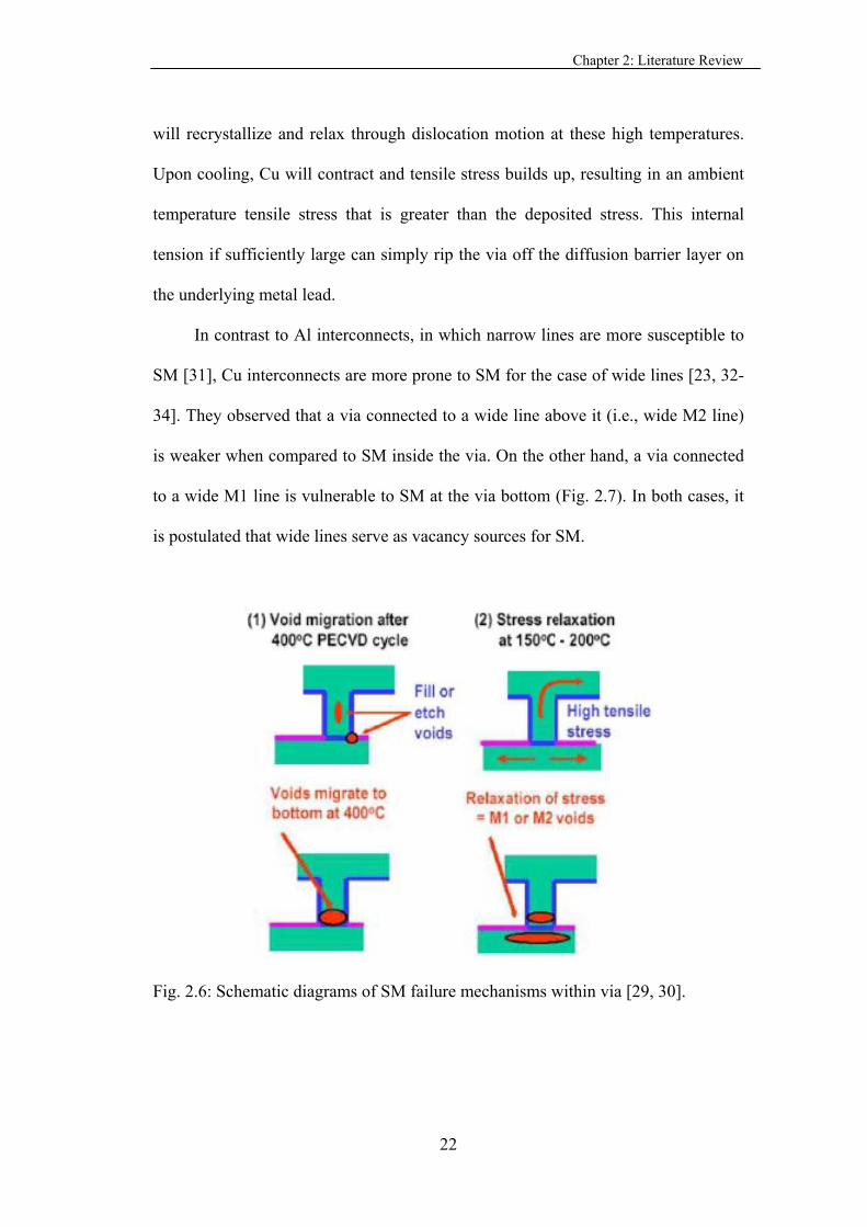
For SM within the via, G. B. Alers et al. [29, 30] proposed two possible
failure mechanisms which cause voiding within a via. As shown in Figure 2.6, the
first SM failure is caused by etch-related or fill-related voids in the metallic Cu that
forms the via. At the high thermal stress, the voids coalesce and migrate to the via
bottom, resulting in an open connection between the via and the diffusion barrier
layer at its bottom. The other failure mechanism is related to the high level of
tensile stress in Cu after a thermal cycle. At high temperature, Cu will expand more
than the oxide trench enclosure thus inducing a compressive stress in Cu. Copper
(a)
(b)
(c)
Chapter 2: Literature Review
22
will recrystallize and relax through dislocation motion at these high temperatures.
Upon cooling, Cu will contract and tensile stress builds up, resulting in an ambient
temperature tensile stress that is greater than the deposited stress. This internal
tension if sufficiently large can simply rip the via off the diffusion barrier layer on
the underlying metal lead.
In contrast to Al interconnects, in which narrow lines are more susceptible to
SM [31], Cu interconnects are more prone to SM for the case of wide lines [23, 32-
34]. They observed that a via connected to a wide line above it (i.e., wide M2 line)
is weaker when compared to SM inside the via. On the other hand, a via connected
to a wide M1 line is vulnerable to SM at the via bottom (Fig. 2.7). In both cases, it
is postulated that wide lines serve as vacancy sources for SM.
Fig. 2.6: Schematic diagrams of SM failure mechanisms within via [29, 30].

Chapter 2: Literature Review
23
Fig. 2.7: Dependence of SM failure rate on the metal width for (a) lower-metal structure and (b) upper metal structure. In both cases, wide metal is more prone to failure compare to the narrow metal [34].
The dependence of SM failure rate on the metal line-width can be explained
using the concept of active diffusion volume (ADV). From a mass transport
perspective, the ADV is defined by a coexistence region among the three volumes
surrounding the vulnerable stress-induced voiding site, i.e., the interconnect
volume, the diffusion volume and the stress gradient. The interconnect volume is
given by the product of length, height, and width within the formation region of the
damage. The diffusion volume is defined by the vacancies supply, which coalesces
to form a void during a given SM test, which depends on the active diffusion
mechanisms present, the stress temperature and the stress time. The diffusion
pathways that define the diffusion volume may be able to extend for long distances
depending on the stress temperature and time. However, a diffusion pathway is
usable only when a sufficient driving force exists. The third is the stress gradient
region where a significant driving force exists to compel vacancies to migrate
towards a specific voiding site. The stress gradient region will depend on the
(a) (b)

Chapter 2: Literature Review
24
geometrical factors that define the interconnect system, material properties of metal,
barrier, dielectrics, and local stress levels developed at the stress temperature.
Assuming the diffusion volume and the stress gradient in narrow and wide
lines to be the same, the differences in the SM failure rate are caused by the
different interconnect volumes. As shown in Fig. 2.8, while in narrow lines only
vacancies beside the via can move towards it; in wide lines, significantly more
vacancies from all directions are available around the via. Consequently, wide lines
can provide more vacancies per time to the via, leading to earlier failure times.
Fig. 2.8: Diffusion area for narrow and wide lines. The wide line is more susceptible to SM failure compared to the narrow line because it can provide more vacancies supply [35].
2.1.3 In-situ Stress Migration
In addition to statistically relevant standard reliability tests and lifetime
analysis, the in-situ study of the void evolution in Cu interconnects caused by SM is
needed to understand kinetics of the degradation process. E. Zschech et al.
presented dynamic studies of damage mechanisms in Cu interconnect caused by SM
[36]. Scanning electron microscopy (SEM) and synchrotron-based transmission X-
ray microscopy (TXM) were applied to visualize the void evolution. SEM
experiments seem to be not very appropriate to study the SIV dynamics during
baking since the focused ion beam (FIB) cut, which has to be located less than 100

Chapter 2: Literature Review
25
nm in front of the Cu via, would intersect the Cu wide line in a region where the
voiding is expected. In the case of TXM, the sample thickness can be larger than 1
μm, and consequently, at least several 100 nm of wide line material exists in each
direction of the Cu via structure.
The test structures were stressed at a temperature of 175°C, a typical
temperature for SM baking. The initial pre-stressing of the sample was performed
for 50 hours. Subsequently, a series of TXM images were recorded after every 5
hours of baking at the same temperature. The time series of TXM images (Fig. 2.9)
shows the void evolution in the Cu interconnect structures. Figure 2.9(a) shows the
TXM image after 80 hours of thermal stressing, without any visible voids, In Fig.
2.9(b), after 90 hours of thermal treatment, an early stage of void formation was
observed in the wide Cu line beneath the via. The void continued to grow during
further thermal treatment, as clearly seen after 95 hours of thermal stress in Fig.
2.9(c). For this particular sample, the void fully encompassed the bottom of the via
after 100 hours of baking at a temperature of 175°C, as seen in Fig. 2.9(d).
In contrast to EM studies, no void movement was observed. Subsequently
after these TXM experiments, the FIB-based serial section technique was used to
create a number of parallel cuts through the wide Cu line and the Cu via, and
particularly around the region where the void was formed. It was found that the
extension of the void is significantly larger than the via cross (see Fig. 2.10). These
experimental results support the SM failure mechanism model proposed by Ogawa
et al.[23], in which vacancies within the ADV migrate along a stress gradient to the
location where the small vias connect wide Cu lines, causing void nucleation and
subsequent growth.

Chapter 2: Literature Review
26
Fig. 2.9: Time series of TXM micrographs showing the void evolution during the SM experiment at 175 °C. The sample was thermally stressed at 175°C for (a) 80 hours, (b) 90 hours, (c) 95 hours, and 100 hours, respectively [36].
Fig. 2.10: Series of SEM images recorded during FIB milling of the SM test structure after the void evolution experiment in the TXM for 100 h at 175 °C [36]. The SEM image series gives an impression about the 3D shape of the void located close to the via.

Chapter 2: Literature Review
27
2.2. Electromigration
The phenomenon of electromigration has been known for over a century
with initial observations reported as early as 1861 by Geradin in molten alloys of
lead-tin and mercury-sodium [37]. During that period of time, the investigations
were primarily basic studies, concentrated mostly on bulk materials. However, EM
did not receive much attention from the engineering community until it was
identified as the root cause of failure in Al interconnect lines in the integrated
circuits of the 1960s [38]. Since then, EM became a key interconnect reliability
concern and a great amount of research and developmental efforts have been
invested towards improving the EM performance.
2.2.1 Fundamentals of Electromigration
Electromigration is a diffusion controlled mass transport of metal atoms,
driven by electron wind current flow in metal lines [39]. As shown in Fig. 2.11,
during electromigration, electrons collide with metal ions transferring momentum to
them, causing metal ions migrate from the cathode and accumulate at the anode.
This significant mass transport during EM results in accumulation of vacancies or
atoms, creating voids at the cathode end and hillocks at the anode end of the
interconnection [39]. The void formation in the interconnection results in an open
circuit or increased line resistance that can cause circuit malfunction. The hillock
formation at the anode terminal of the interconnect can cause a “short circuit”
between adjacent interconnects.

Chapter 2: Literature Review
28
Fig. 2.11: Illustration of the electromigration mechanism. Electrons collide with the copper ions resulting in a momentum transfer to the copper ions, which initiates a mass transport of Cu towards the anode terminal [40].
In general, EM failures are a result of the electron wind forces acting on
metal ions. The electron wind is induced by an external electric field, wherein two
forces act on the copper ions: a direct coulombic force which pulls the ions in the
direction of the applied field and an opposite force resulting from a momentum
exchange with scattering electrons [39]. As the latter force dominates, the electron
wind induces a net material flow and the ions move in a direction opposite to the
field. The electron wind force is generally expressed as [41]
* *elecF e E Z e j
where e* is the effective atomic charge, E is the electric field, Z* refers to the
effective atomic charge number, e is the fundamental electron charge, ρ is the
electrical resistivity of the metal and j is the current density.
(Eq. 2.2)

Chapter 2: Literature Review
29
In the case of an interconnect segment on an IC chip, with rigid dielectric
materials surrounding the metal lines, the motion of atoms leads to mechanical
stress. The cathode end develops a tensile stress due to the depletion of Cu atoms,
while the atom accumulation at the anode end makes it compressive. The flux
divergence results in a stress gradient. This gradient in stress results in a gradient of
the chemical potential and it is often referred to as the “back-stress”. Considering
the back-stress, the net EM atomic flux (J) can be described by Eq. 2.3 [41].
*EM
DC dJ Z e j
kT dx
where D is the Arrhenius temperature dependent diffusivity, C is the concentration
of atoms, k is the Boltzmann’s constant, T is temperature, Ω is the atomic volume,
and dσ/dx is the stress gradient along the one-dimensional (1D) interconnect line.
This atomic flux is mainly the result of two opposing driving forces: the
EWF moving the ions in the direction of the electron flow and a back stress that
pushes the ions in the opposite direction. From this equation, it can be inferred that
the back-stress, which causes a reversal of the migration process, may reduce or
even compensate the effective forward material flow. A steady-state condition can
be achieved when the back-stress balances the EWF component, resulting in a zero
net atomic flux along the line. I.A. Blech pioneered this observation and coined a
condition for EM immunity, which is popularly known as the “Blech-length” or
“short-length” effect criterion [41]. By equating Eq. 2.3 to zero, we can get a
product of length and current density (known as the “jL” product), which can be
used to identify the “immortality” condition:
(Eq. 2.3)

Chapter 2: Literature Review
30
*
nucleationc
jLZ e
where Δσnucleation denotes the stress difference between the cathode and anode
required for void nucleation, L is the line length, and Ω is the activation volume for
EM. Generally, if the critical tensile stress for void nucleation, Δσnucleation, is larger
than the maximum steady state tensile stress developed in the line, no void will
form and the line does not suffer from any EM failure. On the other hand, if (jL)
exceeds critical (jL) product, (jL)c, void nucleation is favored.
After void nucleation, the voids further tend to grow. Depending on the
robustness of the diffusion barrier, which can shunt the electron flow inside the
interconnect and the relative location of the void, it may attain a relatively large size
without causing any open-circuit failure. In this case, the resistance will gradually
increase as the void grows. Growth will eventually stop when an open failure occurs
or when the EM wind force is balanced by the back stress, whichever happens first.
If a force balance develops before the resistance reaches an unacceptably high
value, the segment tends to remain immortal.
The immortality behavior and (jL)c in Cu interconnects have been
investigated by several authors. Generally, there is no standard (jL)c product value
for initiating EM because it is very much dependent on various factors such as the
test structure dimension, dielectric material, metal capping material and process of
fabrication. However, from the (jL)c values reported in the literature, it can be
observed that (jL)c of M1-type structure is relatively lower compared to the M2-type
structure. For the M1-type structure, the reported (jL)c values is 2100A/cm (see Fig.
2.12(a)) [42]. On the other hand, for the M2-type structure, the reported (jL)c values
(Eq. 2.4)

Chapter 2: Literature Review
31
is as high as 3700A/cm (see Fig. 2.12(b)) [43]. The possible reason for this
discrepancy is attributed to the possibility of a void forming directly below the via
to block current flow in an M1-type structure. While in M2-type structure,
immortality requires the small void at the Cu/Si3N4 interface to grow sufficiently to
become a fully-spanning void. The (jL)c was reported to be dependent on the
Young’s modulus of the ILD [44].
Fig. 2.12: The failure distributions of (a) M1-type and (b) M2-type test structures, as a function of the (jL) product. From this figure, it can be inferred that the (jL)c of M1 is 2100A/cm, while for M2, it is ~ 3700A/cm [42, 43].
(a)
(b)

Chapter 2: Literature Review
32
2.2.2 1D Electromigration Model
The most well accepted electromigration model in interconnect lines is the
one proposed by Korhonen et al. [45], along with J.J. Clement et al. [46] in the
early 1990s. The derivations of the relevant concepts presented in their work are
summarized below.
Considering that the atoms migrate via a vacancy exchange mechanism, the
flux of the metal atoms is equal and opposite to the flux of the vacancies. Therefore,
the net vacancy flux can be expressed as
jeZxkT
CDJ vv
v *
where Dv is the vacancy diffusivity and Cv is the vacancy concentration. The
material balance in the line direction gives the continuity equation as:
vCJ C
x t t
In confined metal lines, the relative density change dC/C corresponds to a change in
the stress as:
C
C B
C C
t B t
where B is the effective modulus. Assuming that the vacancies are in equilibrium
with the stress, the vacancy concentration can be written as:
,0 expv vc ckT
(Eq. 2.5)
(Eq. 2.6)
(Eq. 2.7)
(Eq. 2.8)

Chapter 2: Literature Review
33
V VC C
t kT t
where cv,0 is the vacancy concentration in the absence of stress. Combining
Equations (2.5) to (2.9), we can derive a partial differential equation describing the
EM-induced stress evolution in the interconnect. This one-dimensional Korhonen-
Clement model is thus given by
*
1
v v
V
Z e JD C
kT x xCC Bt
B kT C
Due to its non-linearity, and the stress-dependence of Deff, Eq. 2.10 can only be
solved numerically. The stress evolution as a function of location along the
interconnect at different times before and after void nucleation is shown in Figs.
2.13(a) and (b), respectively.
(Eq. 2.10)
(Eq. 2.9)

Chapter 2: Literature Review
34
Fig. 2.13: Stress evolution as a function of location along the interconnect at different time instants in a 1D line segment (a) before (b) after void nucleation [47]. 2.2.3 In-situ Electromigration
In recent years, a number of in-situ electromigration studies have been
carried out on copper lines to understand the dynamics and evolution of the
mechanism. Koetter et al. studied the correlation between void and hillock growth
and microstructure in unpassivated physical vapor deposited Cu lines [48]. K.L Lee
(a)
(b)

Chapter 2: Literature Review
35
et al. carried out Blech-type in situ drift experiments on 10-μm-wide Ta/Cu/Ta and
Ta/Cu(Sn)/Ta sandwich line structures and showed that the addition of Sn reduced
the drift velocity significantly [49]. Proost et al. have carried out drift experiments
on passivated Blech-type test structures looking at the effect of various barrier
layers on the drift velocity in both polycrystalline and bamboo plated Cu structures
[50]. They concluded that the drift proceeds at the Cu/barrier layer interface, with
the highest drift velocity measured in the case of Ta followed next by TaN and then
TiN. A.V. Vairagar et al. clearly observed void formation and migration at the
Cu/dielectric interfaces [51].
In this part, we discuss the observation of in-situ SEM electromigration in
dual-damascene electroplated Cu fine lines with a bamboo grain structure [52].
Figures 2.14.I (a)-(d) consist of SEM micrographs of bamboo-like 0.18 μm wide
line segments tested in series at 260°C with j=1.8 MA/cm2 for a series of testing
times of 0, 9, 46, and 74 hours, respectively. The void growth up to 9 hours appears
to occur by edge displacement. However, it is apparent from a series of SEM
micrographs that the grain ahead of the void front is thinning from the grain surface
for the test time of t = 9 hrs to 46 hrs. Once the grain empties out, the next grain
again thins from the grain surface for t = 46 hrs to 74 hrs. This suggests that surface
diffusion is the dominant diffusion path for void growth. On the other hand, at the
anode end, a large hillock has formed due to the accumulation of copper, as shown
in Figs. 2.14.II (a)-(d).

Chapter 2: Literature Review
36
Fig. 2.14: SEM image of mass depletion at (I) cathode and mass accumulation at the (II) anode end of a 0.18μm wide line at: (a) 0 h, (b) 9 h, (c) 46 h, and (d) 74 h [52].
2.2.4 Electromigration Diffusion Paths in Cu Lines
The microstructure of copper is one of the important factors in determining
the dominant Cu transport path. In a Cu interconnect line, Cu atoms can diffuse
along several paths: bulk crystal lattices, grain boundaries, Cu/diffusion barrier
interfaces and Cu/capping layer interfaces as shown in Fig. 2.15. An expression for
the product of Z* and D for a damascene structure can be written as a weighted sum
of all possible diffusion paths in the interconnect system [53]:
* * * *2 1*
nGBjS
B B B I I I S S GB GBjj
Z D Z n D Z D Z D Z Dw h h d
where the subscripts B, I, S, and GB refer to the bulk, metal/liner interface,
metal/inter-level diffusion barrier surface, and grain boundary, respectively; δI, δS,
(Eq. 2.10)

Chapter 2: Literature Review
37
and δGB, are the width of the interface, surface and grain boundary, respectively; d is
the grain size, w is the line-width, h is the line thickness, and nB, 2 1
I w h
, δS/h,
and (δGB/d) are the fractions of atoms diffusing through the bulk, interface, surface,
and grain boundary of the line, respectively.
Fig. 2.15: Different possible diffusion paths for Cu atoms during electromigration in
the Cu interconnect system.
A range of activation energies for the diffusion along the grain boundary, the
Cu/SiNx interface, grain bulk, and the Cu/Ta liner interface have been reported to
range between 0.7 and 0.95eV [54-56], 0.8 and 1.1eV [35, 57, 58] , 1.53eV [59],
and 0.7 and 1.8eV [60-62], respectively. The top surface of the Cu is reported to be
the fastest diffusion path [53]. Diffusion along the interfaces, such as Cu/SiNx and
Cu/Ta), is highly dependent on their chemistry, bonding and impurity. The large
variation in Ea for the interfaces is likely to be related to the interface property and
materials, and both of these parameters are very sensitive to the fabrication process
conditions. For a typical Cu damascene line, the atomic diffusion at the Cu/Ta liner

Chapter 2: Literature Review
38
interface [61] and bulk diffusion [62] are not considered because of their very slow
diffusivities. As a result, Eq. 2.10 can be simplified as:
* **n
GBjSS S GB GBj
j
Z D Z D Z Dh d
2.2.5 Electromigration Failure Modes
Most of the copper interconnect EM concerns are via-related. Copper
interconnects without via connections typically demonstrate more robust EM
behavior than structures with via connections, assuming no obvious process-
induced defects. Furthermore, failure times for Cu interconnects without via
connections tend to be significantly longer than for their Al counterparts at use
conditions. As a result, most copper EM studies focus only on the via/line
structures.
The direction of the current flow during EM test was found to have a strong
effect on the reliability [63]. EM failures in the dual-damascene copper interconnect
via/line structures can be classified into two distinct modes based on the stress
current directions, i.e., “upstream” and “downstream”. The “upstream” is defined
for the electrons flowing from the lower metal line through via into the upper metal
line and the “downstream” case is defined vice-versa.
Three failure modes were found for the upstream case. The first failure
mode corresponds to a void nucleation and growth at the Cu/Si3N4 interface at the
cathode end of the M2 line (Fig. 2.16(a)) [63]. A void may preferentially nucleate
and grow at the Cu/Si3N4 interface at the cathode end of the M2 line instead of the
via itself, where the tensile stress is expected to be the highest. After a void has
(Eq. 2.11)

Chapter 2: Literature Review
39
nucleated at the Cu/Si3N4 interface of the M2 structure, the void will initially grow
in the direction of the electron flow, resulting in a partially spanning void. As a
result, the resistance of the test structure will increase only slightly while there is
still a high-conductivity Cu path for conduction. An open-circuit failure will result
only when the void grows to span the whole thickness of the metal line. This forces
all the current to flow through the thin Ta liner layer, inducing significant Joule
heating in the liner and leading finally to an open circuit failure.
The second failure mode for the upstream case is a void formation in the
trench of the M2 line (Fig. 2.16(b)) [64]. Trench voiding may occur by grain
thinning in the electron flow direction or by depletion of Cu grains in a step-wise
fashion along the line [65]. Motion and agglomeration of surface voids has also
been reported [51]. If this type of void occurs, a prolonged EM failure time is
observed. In general, a very large void is needed to completely remove the copper
across the line and cause a resistance jump. When a current path through the copper
is interrupted by a large void, the liners across the bottom and sidewalls of the line
shunt the current and show solid redundancy. This is the reason why
electromigration failures caused by voiding may not be a serious reliability concern
for copper lines without via connections.
The third failure mode is the voiding within vias (Fig. 2.16(c)) [66]. However,
this type of voiding is much more strongly process dependent and is typically
observed during early technology development. It can be suppressed by
optimization of the via barrier [67], cleaning, and etch processes [68].

Chapter 2: Literature Review
40
Fig. 2.16: SEM images show various EM failures in M2 line. (a) voids at the cathode end of the M2 line [63], (b) in the trench [64] and (c) inside the via [67].
For the downstream case, three EM failure modes were commonly observed,
i.e., (A) surface voids directly under vias, where the void is in the shape of a narrow
slit, (B) voids under the via, but displaced along the line – length and (C) in the line
attached to the via (Fig. 2.17) [69]. The surface void mode (Case A and B) is an
evidence that the dominant diffusion mechanism of Cu interconnects is the
interface, therefore the void will preferentially nucleate at the Cu/Si3N4 surface near
the cathode end of the M1 line. In Case A, the void is nucleated exactly under the

Chapter 2: Literature Review
41
via. As such voids grow, even a partially spanning void can block current through
the via since the Si3N4 insulator does not provide a conducting path to shunt current.
Thus, a much smaller void volume is required for failure, resulting in shorter
lifetimes. In Case B, the void location is not in contact with the via bottom, but
displaced further downstream in the Cu trench. As a result, the void can grow larger
and cause gradual resistance increase. In Case C, the voiding mechanism of the line
depletion mode is similar to the upstream case. This type of void requires a
prolonged duration of operating time before final failure.
Fig. 2.17: SEM images show various EM failures in M1 test structures: (a) narrow slit void under the via, (b) voids under the via, but displaced along the line-length and (c) void in the line attached to the via [69].

Chapter 2: Literature Review
42
2.3 Effect of Stress Induced Voiding on Electromigration
It is evident from the previous two sections that both electromigration and
stress migration are critical wear-out mechanisms, limiting the lifetime of ultra-
large scale integration (ULSI) copper interconnect systems. Many researchers have
attempted to study the influence of stress voiding on the EM behavior, however the
study is limited to Al-based metallization only. This section summarizes the
literature work aimed at studying the effect of SIV on EM in Al interconnects.
A.S Oates et al. characterized electromigration in narrow, stress–voided
AlSiCu conductors [70]. The effect of passivation stress was investigated in
particular since this parameter has a strong effect on stress-induced void growth.
When the passivation stress is high, so that void growth is not saturated prior to EM
testing, a pronounced degradation of failure time occurs. With a lower passivation
stress, failure times were largely unaffected by SIV. The reliability implications of
the presence of stress voids were also studied in terms of characterizing the current
density exponent of the Black’s equation (n) and temperature acceleration
parameters [70]. It was found that SIV does not affect n, which is close to 2 for both
stress voided and unvoided stripes, and the activation energy remains the same,
which is close to 0.74eV. In addition, the examination of the failed stripes showed
that in metallizations with high stress passivation, pre-existing voids were
preferential sites for EM failure, producing slit-like open circuits as shown in Fig.
2.18. It was proposed that mechanical stress gradients generated by SIV growth are
critical in the processes that result in these open circuits.

Chapter 2: Literature Review
43
Fig. 2.18: An electromigration-induced slit-like opening at the tip of a stress void. Stress voiding gives rise to a wider area of depletion at the top of the stripe [70].
One of the reasons for EM degradation due to stress voiding was proposed by
Matsunaga et al. [71]. He explained that the stress voiding in Al based interconnects
will cause an increase of Al atomic flux divergence during EM test due to the
current crowding and joule-heating effects around the voids. Since the EM time-to-
failure (TTF) is considered to be inversely proportional to the gradient of the flux
density of Al atoms, presence of stress voiding will enhance the EM degradation. It
was found that the size of the SIV is independent of the line-width; hence, the
influence of the voids on the interconnect reliability becomes more severe and
pronounced with decreasing line width.
Further investigations on the growth propensity of pre-existing SIV during
electromigration were performed by C.A Minor et al. using a numerical modeling
approach [72]. Thermomechanical and electrical finite element analysis of voided
metal interconnects were performed. The resulting information was used in
modeling the stress buildup and atomic flux divergence during electromigration
using the finite difference method. A simple correlation between the preexisting

Chapter 2: Literature Review
44
stress-void and electromigration void growth was identified. A large preexisting-
stress void in the metal line is more prone to growth during electromigration than
smaller voids. This is a consequence of the stress gradient along the line generated
by the stress-induced voiding. Therefore, controlling SIV is considered to be an
important criterion in the initiatives to preventing or prolonging electromigration
failure.
The growth of SIV and its influence on the electromigration performance
were studied on different submicron Al-metallization encapsulated in an SiO2
dielectric matrix by A.H. Fischer et al. [73]. The investigations on the EM behavior
revealed a reduction of the Black’s equation current density exponent to n ≈ 1.0 in
metal lines with pre-existing stress-induced voids in comparison to n = 1.7 for good
interconnects (Fig. 2.19). Despite these significant changes, the activation energy
and shape factor (σ) of the EM lognormal failure distribution were observed to be
unaffected by the presence of stress-induced voids. As a consequence, EM lifetime
is significantly reduced in stress-void-damaged metallization. Hence, the influence
of SIV on the EM performance has to be classified as a critical reliability concern.

Chapter 2: Literature Review
45
Fig. 2.19: Determination of (a) current density exponent and (b) EM activation energy for M1-line test structures with and without pre-existing stress-induced voids [73].
2.4 Summary
In this chapter, we summarize the current status of understanding on
interconnect reliability through the literature review of SM and EM in Al and Cu
dual damascene interconnects. The basic understanding and principles underlying
the SM phenomenon such as the stress migration physics, driving force for void
nucleation, various factors affecting its growth such as active diffusion volume and
(a)
(b)

Chapter 2: Literature Review
46
stress gradient were reviewed. Furthermore, the governing physics and opposing
forces of flux for EM were also discussed. The driving forces for void nucleation,
the Blech length (jL product) immortality condition and the effect of varying line
width were also reviewed.
Although SM and EM are generally categorized under different failure
mechanisms for interconnect reliability study, the fundamental physics underlying
SM and EM are “similar”, since both are activated by diffusive mass transport
induced voiding, from different driving forces. Past studies reveal that SIVs would
influence the EM behavior in Al interconnects. It was reported that the EM failure
time was reduced with increasing stress voiding severity. Current crowding and
joule heating around the initial SIV were believed to accelerate the EM degradation.
A large pre-existing SIV in the metal line was shown to be more prone to growth
during electromigration than a small one due to the stress gradient along the line
generated by the void. The current density exponent in the Black’s Equation was
found to decrease in metal lines with pre-existing SIVs.
However, it is noted that the SM and EM interaction study is limited only to
the Al-based metallization structures. Since most advanced technologies now adopt
Cu for the backend and since the Cu interconnect material stack is different from
that of the Al stack, in-depth theoretical and experimental investigations are needed
to understand the SM - EM interaction in Cu/low-κ interconnects.

Chapter 3: Experimental and Simulation Details
47
CHAPTER 3
EXPERIMENTAL AND SIMULATION DETAILS
As shown in the schematic diagram below, the experimental work in this
study can be divided into four main parts: test structure design and sample
fabrication, packaging, accelerated testing and physical failure analysis. The details
of each part are discussed in this chapter.
Fig. 3.1: A sequential flow chart of the experimental work carried out in this study.
3.1 Experimental Setup
The transition from Al to Cu for advanced VLSI interconnects involves
changes in the architecture and the deposition technique. Unlike the direct
patterning process for Al interconnects, no chemicals are available to etch Cu
blanket films to form Cu interconnect lines. Wet etching is not applicable because
Cu is isotropic, while reactive ion etching (RIE) is not practical due to the lack of
volatile compounds at low temperatures. Therefore, Cu-based interconnects are
fabricated using the damascene technique, following the approach to form trench
and via patterns in the dielectric layers by lithography and etching, and filling them
subsequently with Cu as the conductor material by electrodeposition.

Chapter 3: Experimental and Simulation Details
48
The Cu interconnect samples used in this study were prepared by
GLOBALFOUNDRIES, Singapore. The test samples were fabricated using a
standard 45 nm CMOS process on 300 mm wafers, with a single damascene Cu on
metal 1 (M1) and dual damascene Cu on the subsequent via (Vx) and metal leads
(Mx), where x denotes the level of the metallization layer. The schematic diagram of
the dual-damascene process is illustrated in Fig. 3.2.
First, the inter-layer dielectric film stack is deposited on Si substrate by
plasma-enhanced chemical vapor deposition (PECVD) method to give a good film
thickness uniformity and coverage conformity. The dielectrics constant (κ) values
used in this study range from 2.7 to 3.7. After that, the dielectric film is patterned
and etched using photolithography and RIE methods to produce high-aspect ratio
trench/via that define the interconnect layout. Next, a Ta-based film of 10 - 20 nm
thickness is deposited, which serves as an effective diffusion barrier. This is
followed by a Cu seed layer deposited by the physical vapor deposition (PVD)
technique. Cu is subsequently electrodeposited onto the wafer surface. The
microstructures of the electroplated Cu films are found to comprise extremely fine
initial granular structures. In order to enhance grain growth and recrystallization,
the thin film had to be annealed at an elevated temperature. After Cu electroplating,
the Cu overburden and the excess barrier layer at the top surface were removed by
chemical mechanical polishing (CMP), followed by a Si3N4 dielectric cap layer
deposition so that the subsequent interconnect layers can be deposited in a similar
fashion using the same template as the base. These fabrication steps are repeated to
produce the next metallization layer. Finally, the multi-layer metallization was

Chapter 3: Experimental and Simulation Details
49
capped with a thick passivation layer and was subjected to a short duration of
forming gas anneal (FGA) for defect curing.
Fig. 3.2: Process flow for interconnect test structure fabrication involving - (a) Dielectric deposition, (b) Trench / via patterning, (c) Metal barrier deposition, Cu seed deposition and Cu electroplate fill, (d) Cu and metal barrier CMP and (e) Nitride barrier passivation.
The SM and EM accelerated tests were carried out at a package level, which
means the wafer was diced, the dies were attached and wire bonded to a ceramic
(a) (b)
(c) (d)
(e)
Dielectrics
Si3N4

Chapter 3: Experimental and Simulation Details
50
package for thermal and/or electrical stress testing. The reliability assessment was
preferred in the package-level than wafer-level because of long measurement time.
The packaging process was carried out at the Singapore Institute of Manufacturing
Technology (SIMTech), A*STAR.
The first packaging step involves mechanical dicing to cut the Si wafer into
individual chips. It was carried out by a full cut dicing method using a Disco DAD
341 dicing system. As a preparation step for dicing, the wafer was mounted on a
dicing frame using ultra-violet dicing tape which has a base film and adhesive layer
on top. The cutting tool, which is called as the dicing blade, was mounted in the
spindle of the dicing equipment. Then, the wafer was mounted in the wafer frame
held in a vacuum chuck, which moved at a specific feed rate passing through the
dicing blade in the X and Y directions. The wafer was carefully diced because
cracks can be easily generated in the low-κ material. To minimize crack and
delamination, the dicing was performed in a surrounding presence of guard rings
and the dicing blade was set to rotate at a relatively slow speed of 29,000 rpm. The
guard ring prevented the moisture penetration into the devices through the edge of
the chip. As shown in Fig. 3.3, the dicing cut method used was a single cut. It is a
conventional method of singulating the chips by using one blade and one spindle in
a single pass.
After wafer dicing, the selected samples were packaged in 24-pin dual-in-
line ceramic packages (DIP) with a die-attach silver paste, and then cured in a
vacuum oven at 120˚C for 5 minutes to improve the adhesion. Next, the chip bond
pads were wire-bonded to the lead frame for electrical connection. An example of
the wire bonding schematic diagram is shown in Fig. 3.4. The pin-to-pin resistance

o
u
p
Fw
Fb
of all the s
under the
performed.
Fig. 3.3: (a)wafer into in
Fig. 3.4: (a)bond pad to
(a)
tructures w
optical mi
) Mechanicndividual ch
) Schematic the lead fra
was measure
croscope to
cal dicing prhips. (b) A p
c diagram ofame. (b) A p
C
51
ed using a
o ensure t
rocess usinphoto of a d
f wire bondphoto of a p
Chapter 3: Exp
multi-mete
that the w
ng the singlediced Si wa
ding. The wipackaged di
(b)
perimental and
er, and they
wire bondin
e cut methofer.
ires shown ie.
d Simulation D
y were insp
ng was pro
od to dice t
connect the
Dicing tape
Si wafer
Details
pected
operly
the Si
e chip
e

Chapter 3: Experimental and Simulation Details
52
3.2 Testing and Analysis
3.2.1 Electrical Testing
Assessing the EM and SM reliability under normal operating conditions is not
practical to due to the extremely long testing time needed to observe sample
failures. Thus, a more realistic accelerated lifetime testing is usually conducted at a
high temperature and high current density stress for EM or at a medium temperature
for SM, i.e., 150-200˚C. The testing results can then be extrapolated back to the
normal operating conditions using suitable physical / empirical extrapolation
models. For stress migration, the extrapolation of the TTF from the high storage
temperature to the operating temperature conditions can be carried out using the
model in Eq. (3.1), prescribed in [74]:
2
1* exp a
strB
TTFE
Ck TT
where C* is a constant, ΔT is the difference between the effective passivation
deposition temperature and the storage temperature (Tstr). For electromigration, the
basis for such an extrapolation is the Black’s empirical equation, expressed in Eq.
(3.2) [75]:
expn aETTF Aj
kT
where A is an empirically determined constant, j is the current density, n is the
current density exponent typically ranging between 1 and 2, and Ea is the activation
energy for the limiting diffusion path. It has been shown that a current density
Eq. (3.1)
Eq. (3.2)

Chapter 3: Experimental and Simulation Details
53
exponent of n = 1 is consistent with void-growth-limited failure, while an exponent
of n = 2 indicates void-nucleation limited failure.
The standard test method for stress migration test is relatively straight
forward. SM tests are typically carried out at the wafer level. The resistance of the
test structures is measured before baking. The total duration for baking is
conventionally 1000 hours, with resistance measurements recorded at intermittent
points of time, e.g. 250, 500, 750 and 1000 hours. The wafers are cooled to room
temperature before each resistance measurement and then returned to the baking
temperature. Resistance of the test structures that are obtained after each exposure
to baking are compared to the initial resistances and any failures, if detected, are
recorded down. Failure is defined as a resistance increase greater than a predefined
amount, typically 10% from the original value.
However, from a practical viewpoint, SM test is not easy to be performed
because of the long test duration. Tests that last 1000 hours correspond to an overall
duration of about 6-8 weeks, including the testing time and data analysis.
Furthermore, in contrast to EM, where the entire sample can be forced to fail, often
only a small population of samples encounters SM failures. The small amount of
data collected limits the failure distribution characterization and failure rate
projection to the use condition. Considering these difficulties, IC manufacturers
often choose to improve the process until no measurable SM behavior is evident in
the metallization. This does not mean that the metallization is void free. Rather, it
means that no void grows large enough to cause a measurable resistance shift by the
end of a product life.

Chapter 3: Experimental and Simulation Details
54
As shown by Eq. 3.2, EM test can be accelerated by increasing the current
density and / or the temperature. While EM stresses for Al interconnects were
carried out at around 250°C, Cu EM structures were tested here at 300°C or more,
in order to keep the stress duration short and reasonable. The EM test was
performed using a XACT-810 EM-tester which can host 64 test structures
simultaneously. This is an in-situ test system, where the resistance change is
monitored continuously with a high measurement resolution. A Keithley 2000
multi-meter was used to measure the individual voltage drops across each test
structure. A photograph of the EM testing chamber is shown in Fig. 3.5.
During the EM test, there are two parameters that need to be precisely
controlled: the testing temperature and the current density. Such control is necessary
for appropriate EM lifetime extrapolation from the stress conditions to the regular
operating condition. In order to achieve adequate temperature control during the
experiment, a thermocouple was installed in the chamber to measure the ambient
temperature and to provide feedback to the temperature controller. The constant
current condition was adjusted and maintained by a current regulating board. As a
result, the EM testing system offers effective regulation of both the stress
temperatures and the current densities. The current fluctuation was very minimal
and the temperature variation was less than 0.2°C.

Chapter 3: Experimental and Simulation Details
55
Fig. 3.5: Photo of the (a) EM testing chamber of a XACT-810 EM tester and the (b) burn-in-board to place the samples for testing.
3.2.2 Physical Failure Analysis
Extensive failure analysis of selected failed samples was carried out to
observe the void morphology using either the SEM or transmission electron
(a)
(b)

Chapter 3: Experimental and Simulation Details
56
microscope (TEM). However, since some of the test structures used in this study are
via chain structures which consisted of a large number of vias, advanced failure
localization technique is required. In this study, passive voltage contrast (PVC)
technique and thermally induced voltage alteration (TIVA) methods were used to
isolate and locate the failure site in the complex via chain structure.
PVC technique was used when there is a very high resistance defect in the
via chain, such as an open via. The experimental procedure can be described as
follows: at first, RIE and mechanical polishing were employed to selectively
delayer the dielectric layers and Cu metal leads until the top metal of the stress-
induced damaged via chain was physically revealed. During PVC analysis using
SEM, an Al pad of the via chain structure was grounded and the electron beam
accelerating voltage was adjusted to maximize the secondary electron yield. The
defect essentially divided the structure into a grounded region and a floating region.
This difference in potential generated a different secondary electron yield from each
of these regions thereby enabling the failure analyst to identify the location of the
defect at the boundary between the two regions.
As seen in Fig. 3.6, at areas where there is a discontinuity, the secondary
electrons generated were attracted by the positive potential surface; thus these
regions appeared dark. On the other hand, at areas with good connectivity, the
surface of the sample would be grounded and the secondary electrons generated
could be detected by the electron beam detector; hence these regions appeared
bright. The difference in the contrast helped to locate the failed via easily.
Subsequently, TEM analysis was performed to study the void morphology and infer
the associated failure mechanism.

Chapter 3: Experimental and Simulation Details
57
Fig. 3.6: PVC image of a via chain test structure after SM test to localize a defective metal area [76].
While PVC was used to locate a high resistance defect, TIVA is more
sensitive in locating the defect. For TIVA, the sample was scanned with an infra red
laser beam whose wavelength is 1340 nm. The sample was biased with constant
current and the voltage was monitored. As the laser striked the defect location, the
resistance change due to thermal effect and the measured voltage changed
accordingly. Through this approach, the location was recorded and correlated to the
sample.
3.2.3 Joule Heating Test
The purpose of quantifying Joule heating in the interconnects is to determine
the maximum current density that can be applied at EM accelerated testing
experiments. Significant Joule heating caused by resistive heating may occur when
lines are stressed at very high current densities. Since diffusivity is highly
temperature dependent, these temperature gradients will induce mass flux
Dark
B Bright
Failure

Chapter 3: Experimental and Simulation Details
58
divergences that may not occur at use conditions. To minimize this effect, the
average temperature increase due to Joule heating is kept below 4 K.
The average Joule heating of the whole interconnect at the test temperature
was estimated by first measuring the temperature dependence of the resistance at
low current densities (in order to have only a negligible amount of Joule heating).
The experiment was performed using a wafer level four point measurement
technique. Then, the resistance was measured as a function of the current density at
the test temperature. The resistance change of the metal line with temperature is
defined by the following equation:
0 (1 )R R T Eq. (3.3)
where R0 is the initial resistance of the line, and α is the temperature coefficient of
resistivity (TCR). The TCR of the line was determined from the slope of the
resistance vs. the temperature graph. Next, the sample was maintained at the EM
test temperature while the current density was increased. From the change in the
resistance as a function of the current density, the amount of Joule heating was
calculated by:
0
1RR
T
Eq. (3.4)
Figure 3.7 shows an example of joule heating measurement for a 400μm long,
0.58μm wide M1 test structure. The test structure used in this experiment is a four-
terminal EM structure, shown in Fig. 3.7.

Fh
F
o
F
3
c
M
f
t
=
Fig. 3.7: Scheating test.
First, a nom
order to ob
From the slo
3.33x10⁻³ K
condition o
MA/cm2. U
fig. 3.8 (b),
temperature
= 6.2 MA/cm
chematic di.
minal curren
btain the res
ope of the g
K-1. Subsequ
of 350˚C, t
Using Eq. 3.4
even the m
e without ca
m2.
agram of th
nt density (<
sistance val
graph, it wa
uently, whi
the current
4, the amou
maximum cu
ausing signi
C
59
he four-term
< 0.1MA/cm
lue at temp
as estimated
ile the tem
density w
unt of joule
urrent dens
ificant Joule
M1
Chapter 3: Exp
minal EM t
m2) was pas
peratures ra
d that the TC
mperature w
was ramped
heating ca
ity can be s
e heating. N
Bondpa
perimental and
test structur
ssed through
anging from
CR of the te
was fixed a
d from 0.2
n be obtain
safely appli
Note that ∆T
M2
ad
d Simulation D
re used for
h the structu
m 100 to 35
est structure
t the EM
MA/cm2 t
ned. As show
ied at 350°C
T < 4 K eve
Details
joule
ure in
50°C.
e was
stress
to 10
wn in
C test
en at j

Chapter 3: Experimental and Simulation Details
60
Fig. 3.8: Joule heating measurement for a Cu-based interconnect structure. (a) Resistance vs. temperature at nominal current density, (b) rise in temperature, ∆T, as a function of the current density, j, which is increased to an extreme value at elevated temperature over a short span of time.
3.2.4 Statistical Analysis
Electromigration-induced failures are stochastic in nature, therefore the EM
failure time for any given population of interconnects is not deterministic, but
governed by a statistical probability (cumulative failure) distribution instead. It is to
be noted that most of the literature reports used the monomodal lognormal
(a)
(b)

Chapter 3: Experimental and Simulation Details
61
distribution to describe the scatter of electromigration lifetime data, although the
justifications are mostly empirical. As described in Chapter 2.2.5, there are several
EM failure mechanisms for the same stressing conditions, and different underlying
thermally driven failure mechanisms will have different failure time distributions
(median failure time and spread of the failure data), with different statistical
distribution parameters. EM failures caused by voiding in the Cu line at locations
separated from the via usually have longer failure times, than those caused by
voiding associated with the via bottom.
As will be discussed in Chapters 5 and 6, the experimental results show that
the failure time for samples under the SM+EM test were widely distributed and the
failure distributions did not show monomodal lognormal behavior. Therefore, in
this study we use a statistical algorithm using the Akaike information criterion
(AIC), Expectation and Maximization (E&M) algorithm and the Bayes’ posterior
probability theory to identify the number of underlying failure mechanisms
embedded in a given set of test data and classify the failed units belonging to each
of these different mechanisms. The details of the adopted algorithm for this
statistical approach are summarized below [77].
To identify the number of underlying physical failure mechanisms contained
in the set of test data, the AIC was employed [78]. This AIC is a measure of the
goodness-of-fit of a proposed statistical mixture model. It is used to determine the
optimal number of mixture components that fit a given set of failure data. The
expression for AIC is given by Eq. 3.5, where L is the maximum likelihood
estimation (MLE) of the fitted model and m is the number of degrees of freedom
(D.O.F.) in an n-component mixture distribution. The relationship between m and n

Chapter 3: Experimental and Simulation Details
62
is given by m = 3n − 1. The term (2m) in Eq. 3.5 is the penalty factor that prevents
too many mixture components to be redundantly added to fit the data more
accurately. The number of components n, for which the AIC is the lowest is found
to be the best-estimate for the number of distinct component distributions (failure
mechanisms) in the test data:
2 log 2AIC L m
After determining the number of failure mechanisms, the E&M algorithm was
used for the analysis of the mixture distribution [79-81]. It determined the
distribution parameters by maximizing the log-likelihood function of the mixture
distribution. Here, the E&M algorithm was applied to the case of a three-parameter
lognormal mixture.
The probability density function (p.d.f), f (t), for a three parameter lognormal
model is given by Eq. 3.6 where t50 is the median-time-to-failure; σ is the shape
parameter and X0, the failure-free time [82]. Since no failures can occur before the
failure-free time, f (t) = 0 for t < X0:
2 0
50 050 0 02
0
50 0 0
ln1
; , , exp ,2( ) 2
; , , 0,
t X
t Xf t t X t X
t X
f t t X t X
Eq. (3.5)
Eq. (3.6)

Chapter 3: Experimental and Simulation Details
63
The p.d.f. for a n-component mixture distribution, f (t), is generally expressed
as in Eq. 3.7, where pi represents the mixing weight, Θi represents the set of
lognormal parameters [t50(i),σi,X0(i)] and fi(t) is the p.d.f. expression for component i
of the mixture. The sum of all the mixing weights is equal to 1. The component with
the highest mixing weight is the dominant failure mechanism.
1 1
| | , 1n n
i i i ii i
f t p f t p
For a two-component lognormal mixture, the effects of the failure-free time for the
two different components, denoted as X0(1) and X0(2) respectively are included, and
the overall mixture p.d.f. may be expressed as in Eq. 3.8:
0(1)
1 1 1 0(1) 0(2)
1 1 1 1 2 2 0(2)
| 0,
| ,
| (1 ) | ,
f t t X
p f t X t X
p f t p f t t X
The log-likelihood function (L) for a three-parameter lognormal mixture is given by
Eq. 3.9 where tj represents the jth failure data. Based on Eq. 3.9, the best-fit
distribution parameters are obtained by solving the four partial derivative
expressions in Eq. 3.10:
50 0( )
| ln | ln !
0
jj
i i i i
L t f t n
L L L L
p t X
These expressions can be modified to give equations Eq. 3.11 - Eq. 3.13, which are
easier to solve. The expression Pr(i|tj) in Eq. 3.11 is the probability that a failure
Eq. (3.7)
Eq. (3.8)
Eq. (3.9)
Eq. (3.10)

Chapter 3: Experimental and Simulation Details
64
unit which fails at time t = tj belongs to component i of the mixture distribution. It is
called the posterior probability, and it is obtained from Bayes’ theory [80]. The
symbol y in Eq. 3.13 represents either t50, σ or X0 as required:
50( ) 0( )
50( ) 0( )
50( ) 0( )
50( ) 0( )
| , ,Pr |
| , ,
1Pr |
ln | , ,Pr | 0
, ,
i j i i i
j i
i i j i i iall i
i jj
i j i i i
jj
i i i
f t t Xi t p
p f t t X
p i tn
f t t Xi t
y
y t X
Equations 3.11 - 3.13 were numerically solved using the Matlab software to obtain
the distribution parameters.
3.3 Simulation Details
A finite element modeling (FEM) and simulation approach was developed to
understand the hydrostatic stress distribution in Cu interconnects, which is
important to study the tendency for vacancy migration during SM and investigate
the influence of interconnect geometry and dielectric material scenarios.
Differential thermal stresses are generated in the Cu line-via structures during
temperature cycling and at use condition. The thermal stresses generated in the Cu
films and Cu lines are different. The thickness of a Cu film could be small, but its
in-plane dimension is relatively large, resulting in a biaxial stress state. In a Cu line,
the tri-axial stress state is expected since the sidewalls of the line are confined by
the diffusion barrier and the dielectrics. Furthermore, plastic deformation behavior
Eq. (3.11)
Eq. (3.12)
Eq. (3.13)

Chapter 3: Experimental and Simulation Details
65
is also different due to much smaller dimension of Cu lines. As the thickness of the
Cu lines decreases, the yield strength is expected to be higher according to the Hall-
Petch relationship. Therefore, thermal stress behavior of Cu films might not be a
suitable model system to analyze the stress related failure mechanisms in Cu lines.
There are two ways to understand the stress distribution in the Cu
interconnects, i.e., through measurement and/or modeling. The stress in the
interconnect can be measured experimentally by wafer curvature and x-ray
diffraction (XRD) technique. However, the current stress measurement technique is
limited only to simple test structures. It has insufficient spatial resolution to
determine the detailed stress distribution in complex interconnect systems. Hence,
FEM has been extensively used for detailed stress distribution analysis. During the
last few years, XRD measurements [24] have been used to validate the stress
modeling theory.
3.3.1 Finite Element Simulation Model Approach
The FEM was built using the commercial ANSYS® software by assuming
isotropic material properties with linear elastic behaviors [24]. The high yield
strength of thin and narrow lines is explained by the limited grain size and the
restrained dislocation movement due to increased interface area of contact [83-85].
In general, the model development comprises three steps.
A. Preprocessing
In this stage, the geometry of the test structure is designed, structured mesh
for each volume is created, suitable material properties are assigned and appropriate
initial and boundary conditions are applied. The type of element used in this

Chapter 3: Experimental and Simulation Details
66
simulation is a 3D solid structure, i.e., “solid 45”. It has eight nodes having three
degree of freedom with each node translating in the nodal x, y, and z directions. The
boundary conditions used in the simulation are defined as follows:
1. The bottom plane is assumed to be rigidly clamped onto the substrate, thus
no displacement is allowed in any direction, i.e., ux=uy=uz=0. (Note: The
symbol u means displacement, e.g. ux means displacement in the x
direction).
2. The top surface is free to move during deformation.
3. The structure was considered to be arrayed periodically along the x and y
directions, mirror symmetry normal to each surface. All interfaces were
assumed to have perfect adhesion, therefore no displacement is allowed in
the x and y directions.
B. Solution
During the solution phase of the analysis, the governing equations for each
element are formulated, assembled into matrix form and then solved numerically by
the computer. The stress free temperature was set to 300°C [15] and the simulations
were carried out at an SM-test temperature of 200°C.
C. Post-Processing
This is the last stage in the FEA process wherein the results are visualized
within the FEA environment. Numerical and graphical tools are used to analyze the
stress distribution in the designed model.
3.3.2 Validation of Stress Simulation Model

Chapter 3: Experimental and Simulation Details
67
The stress simulation model developed in this work was verified using the
simulation and experimental stress measurement data reported by S.H. Rhee et al.
[24]. In order to evaluate the validity of our FEM model, the computed results were
compared against data from volume-averaged thermal stresses in Cu, measured by
XRD. XRD is a commonly used technique for measuring stresses in thin films and
interconnect lines. As shown in Fig. 3.9(a), the method of this measurement is to get
the change in the lattice parameter of the Cu lines in the stressed state. The plane
spacing was measured at different inclination angles (ψ) to the surface normal and
rotation angles (hen a linear relation between the lattice spacing (d) and sin2ψ
was used to determine the principal strains as shown in Fig. 3.9(b). The
corresponding strain was finally transformed to obtain the stress value [24].
As described in [24], the test structures used for stress measurement
correlation were arrays of parallel Cu lines in TEOS oxide processed by a
damascene patterning. A 0.5μm thermal oxide was grown on top of the 8 inch
wafers. A blanket 0.6μm TEOS oxide film was then deposited on this 0.5μm
thermal oxide. Following this, 0.6μm deep trenches were patterned in the TEOS
oxide and a 40 nm Ta barrier layer was deposited prior to the deposition of a Cu
seed layer and Cu electrochemical deposition. The excess Cu over the lines was
removed by CMP. Finally, a 50 nm SiN capping layer was deposited, followed by
the deposition of a 0.4μm thick TEOS oxide. Four different dimensions for the
interconnect lines were reported for nominal widths/pitches: 1.0/2.0μm, 0.6/1.2μm,
0.4/0.7μm, and 0.25/0.55μm. The slopes of the stress–temperature curves, (dσ/dT),
obtained from our FEA-based on the simplified 3D models were compared with
those measured by the XRD method for TEOS. This method is preferable rather

Chapter 3: Experimental and Simulation Details
68
than comparing the absolute stress value because the zero stress temperature varies
depending on the process conditions in the experiment. Therefore, the slope is a
more consistent parameter to use for comparing the stress characteristics of
different samples.
Fig. 3.9: (a) XRD measurements of the thermal stress and (b) the linear relation between lattice spacing and sin2ψ used to determine the principal stress / strain values [24].
(a)
(b)

Chapter 3: Experimental and Simulation Details
69
Considering the mirror symmetry condition in the simulated structure, a
simplified half-line model was employed in this study as shown in Fig. 3.10. All
interfaces in the structures were assumed to be perfect, and the metal lines were
considered to behave elastically within the temperature range of the XRD
measurements. Using the thermo-mechanical properties of the materials, boundary
conditions, and stress free temperature data provided in [24], the thermal stress
simulation was executed using our model. The results of the stress simulation in x,
y, and z directions can be seen in Fig. 3.11. In general, the results obtained from the
finite element analysis (see Fig. 3.12(b)) are in good agreement with the reported
simulation and experimental data (as shown in Fig. 3.12(a)). Hence, our model is
verified to be reasonable for stress simulation studies.
Fig. 3.9: A unit segment of the Cu interconnect structure showing finite element “mesh” discretization used for the calculations. Considering the symmetry, only a half-line model was employed.

Chapter 3: Experimental and Simulation Details
70
.
Fig. 3.11: Stress component distribution for various line-width/pitch dimensions in the simulated Cu/SiO2 model.
Cu line
Cu line
Cu line

Chapter 3: Experimental and Simulation Details
71
Fig. 3.12: (a) Comparison between the measured X-ray data and FEA results for TEOS passivated Cu lines as reported by S.H. Rhee et al. [24]. (b) The thermal stress data obtained from the simulation model developed in this work.
3.3 Summary
In this chapter, a detailed description of the experimental and simulation
procedures adopted for the Cu interconnects SM-EM reliability study was
presented. In the first part, we discussed the experimental procedure consisting of
test structure design and sample fabrication, packaging, accelerated testing and
physical failure analysis. The fabrication process for the Cu interconnects test
structure using the damascene technique and detailed descriptions of the packaging
(a)
(b)

Chapter 3: Experimental and Simulation Details
72
process were presented. After that, we elaborated on the standard SM and EM tests
and the details of the physical analysis methods employed to examine the failure
defect were discussed.
In the second part, we presented the approach for our simulation work. A
finite element model was developed to understand the hydrostatic stress in Cu
interconnects, which is important to study the vacancy migration tendency during
stress migration and investigate the influence of interconnect geometry and
dielectric material properties. In order to evaluate the validity of the FEM model,
the computed simulation results were compared with the experimental data
imported from literature.

Chapter 4: The Effect of Dielectric Slots on Cu Interconnect Reliability
73
CHAPTER 4
THE EFFECT OF DIELECTRIC SLOTS ON CU
INTERCONNECT RELIABILITY
4.1 Introduction
As introduced in Chapter 1, the integration of low permittivity dielectric
materials in the copper interconnects backend network has become very critical,
considering the need for faster response devices (lower RC delay) in addition to
miniaturization. However, the implementation of low-κ and replacement of SiO2
has posed new challenges to both stress migration and electromigration reliability
(and dielectric breakdown as well). It has been reported that Cu interconnects with
low-κ ILD have a shorter SM lifetime compared to FTEOS [14]. Moreover, studies
have shown that the presence of low-κ material enhances the mass transport
kinetics for Cu migration during EM due to degraded thermo-mechanical properties
of the stack and poor interface adhesion [44].
Generally, there are two approaches to improve the robustness of Cu
interconnect reliability. Firstly, the system can be improved through process
optimization, such as alloying the Cu [86, 87], replacing the traditional dielectric
cap with a metal cap [62, 88], optimizing the thermal annealing process and re-
sputtering step during PVD process for the diffusion barrier layer [89], etc.
Secondly, the system can be improved through alteration of the interconnect design.
One such approach is to add redundant vias in the metal line. Previous work has
shown that employing a parallel configuration of multiple Cu vias helps to improve

Chapter 4: The Effect of Dielectric Slots on Cu Interconnect Reliability
74
the robustness of Cu interconnects towards both SM and EM failures [90-92].
Another approach is where the dielectric slot of the Cu interconnect is redesigned.
This method is reported to be able to suppress SM failures [95, 96]. The dielectric
slot here refers to a redesigned small dielectric block, which is commonly used in
wide Cu metal leads to prevent dishing during the CMP process.
In this chapter, we study the individual SM and EM reliability of Cu
interconnects in the presence of the dielectric slots. The possible SM and EM failure
mechanisms and design and process integration challenges are discussed. The
purpose of this work is to gain a good understanding of the SM and EM behavior in
our test structures, as a basis to later investigate the interaction between these two
failure mechanisms.
4.2 Fabrication Scheme of Cu Interconnect with Dielectric
Slots
Figure 4.1 shows the schematic diagram of the test structure with a small
dielectric slot in a wide bottom Cu metal lead (M1). This dielectric slot is
incorporated into advanced Cu interconnects using a damascene process without
additional masking steps. The fabrication process is described by the following
steps (Fig. 4.2).
(a) First, M1 and a rectangular dielectric slot were masked together after the
inter-layer dielectric (ILD) CVD process. The ILD material was a carbon-doped
oxide, SiCOH (κ ~ 3).

Chapter 4: The Effect of Dielectric Slots on Cu Interconnect Reliability
75
(b) During the etch process, the rectangular dielectric slot was patterned within
the wide M1. The location and shape of the dielectric slot has to be designed
carefully as it will affect the interconnect resistance and reliability robustness.
(c) Then, Cu was electroplated on its seed layer template and was annealed at an
elevated temperature.
(d)/(e) Following this, the redundant Cu was removed by a CMP process and the
Cu surface was passivated with a layer of Si3N4. Thereafter, the M1 dielectric
slot was formed.
Fig. 4.1: Schematic diagram of the top view of the dielectric slot in the bottom Cu metal lead (M1).
Fig. 4.2: Schematic diagrams illustrating the process flow involved in patterning and fabrication of the dielectric slot in the wide bottom Cu metal lead level.

Chapter 4: The Effect of Dielectric Slots on Cu Interconnect Reliability
76
4.3 Design Integration Challenges
As will be discussed in section 4.4, the location and shape of the dielectric
slots was found to be very crucial in determining the SM reliability improvement.
The dielectric slot, which is incorporated near the via, is more effective in lowering
the tendency for void nucleation (discussed in section 4.6). In addition, the
dielectric slot must be sufficiently long to effectively impede vacancy coalescence
in Cu interconnects for SM reliability improvement, and yet have a minimal effect
on the interconnect resistance increase and EM performance. A very long dielectric
slot will increase the interconnect resistance drastically and degrade EM
performance (due to current density increase at the metal lead beside the dielectric
slot). Hence, a balance between good reliability and electrical performance has to be
achieved through appropriate design of experiment (DOE) and optimization.
The effect of the dielectric slot design and location on the electrical
performance can be predicted by a resistance calculation. Assuming a 2μm x 10μm
metal lead, with a rectangular dielectric slot, the interconnect resistance
dependencies on the width and the length of the dielectric slot are shown in Fig.
4.3(a) and (b). The interconnect resistance changes exponentially with the dielectric
slot length (L) and linearly with the dielectric slot width (W). Its resistance could
increase by more than 25% if an inappropriate choice of the slot length is made.
Thus, an optimum length has to be chosen to prevent any significant increase in the
interconnect resistance and simultaneously, it should still serve as a good impeder
against vacancy coalescence. In addition to that, the dielectric slot width has to be
designed to be sufficiently wide. A narrow slot poses difficulty in process

Chapter 4: The Effect of Dielectric Slots on Cu Interconnect Reliability
77
integration. During the masking and etching processes, narrow photo-resists tend to
topple easily and causes distorted or missing patterns.
Fig. 4.3: Impact on interconnect resistance for varying dielectric slot dimensions. (a) Slot length, L, varied with a fixed width of 0.3μm and (b) Slot width, W, varied with a fixed length of 1.2μm. The insert shows the location of a 0.19μm via in a 2μm x 10μm Cu metal lead [95].
4.4 Effect of Dielectric Slots on Stress Migration Reliability
Figure 4.4(a) shows the experimental result of a SM test at 200°C for 1000
hours. It shows that the SM reliability of the wide bottom Cu interconnects with the
dielectric slot is more superior to that without the dielectric slot. Moreover, as
illustrated in Fig. 4.4(b), the SM reliability of interconnects with dielectric slots and
dual-via interconnects, known to improve SM robustness [93, 94], is comparable.
This observation was further supported by a physical analysis performed on stressed
structures. Fig. 4.5(a) shows that in the absence of the dielectric slots, a stress-
induced void was formed beneath the via and extended significantly into the wide
Cu metal lead. On the other hand, as shown in Fig. 4.5(b), no voiding was observed
in the presence of a dielectric slot close to the via [95]. The impact of dielectric slot
on the interconnects resistance was minimal, i.e. ~1.7% increment [95].

Chapter 4: The Effect of Dielectric Slots on Cu Interconnect Reliability
78
Fig. 4.4: (a) SM reliability improves drastically for wide bottom Cu interconnects with dielectric slots. (b) Similar SM robustness is demonstrated for wide bottom Cu interconnects with dielectric slots as compared to that with dual-via structures [95].
Fig. 4.5: Significant improvement of SM reliability for wide Cu interconnects with dielectric slot. Physical failure analysis of wide Cu metal leads after SM Test for (a) a conventional test structure shows significant voiding extending into the Cu line, while for the (b) test structure with a dielectric slot, no voiding was observed [95].
(a)
(b)
(a) (b)

Chapter 4: The Effect of Dielectric Slots on Cu Interconnect Reliability
79
Further studies were carried out by G.D.R. Hall et al., who compared the
effect of the dielectric slot for different sizes and locations on the SM robustness
[96]. As shown in Fig. 4.6, it was reported that the metal lead without dielectric slot
has the highest failure rate and dielectric slots placed near the via show the lowest
failure rate. Moreover, longer slots are proven to be more effective in suppressing
stress-induced failure than segmented slots [96].
Fig. 4.6: Cumulative failure distribution plot for SM tests on different dielectric slot design structures. The control sample with no dielectric slot had the highest failure rate, followed by the segmented slots at the center of the block, long slots at the center of the block and long slots at the edges of the block, near the via [96].
Long Edge Long Center Segmented Center

Chapter 4: The Effect of Dielectric Slots on Cu Interconnect Reliability
80
4.5 Effect of Dielectric Slots on Electromigration Reliability
In this part, we evaluate the electromigration reliability of interconnects with
the dielectric slot in the lower metal line (M1). The length and width were 400μm
and 0.58μm, respectively, while the M2 line was broader and shorter. The via
diameter was fixed at 0.14μm and the dielectric slot size was 0.3X0.3μm slot. The
distance between the dielectric slot and via was 0.12µm. The samples were stressed
at a 1.5MA/cm2 current density (line) and at a temperature of 350˚C. The failure
criterion used is the standard 10% increase in resistance.
The relatively low current density stress was selected to minimize Joule
heating induced failures, especially at the sides of the dielectric slotted metal lead
(M1). It was found that the stressing current density can be as high as 3MA/cm2 at
the sides of the dielectric slot. The TCR and average Cu interconnect temperature
increase due to Joule heating was measured using a wafer level 4-point probe
measurement technique. The TCR for the dielectric slot structure was calculated to
be 0.00333K-1 and the line average temperature increase is 0.1ºC at 1.5MA/cm2 test
condition (Fig. 4.7). It was estimated that the temperature rise at the side of the
dielectric slot was 0.2ºC; giving rise to a negligible temperature increase in the Cu
region next to the dielectric slot.

Chapter 4: The Effect of Dielectric Slots on Cu Interconnect Reliability
81
Fig. 4.7: Joule heating four-point probe measurement of the temperature rise (∆T) in conventional and dielectric slot test structures.
Figure 4.8 shows the lognormal EM failure time distributions for the
standard and dielectric slot test structures. Interestingly, the median times to failure
(t50) for both the test structures are similar. There was no notable lifetime
degradation due to the dielectric slot or lifetime improvement as what we found for
the SM phenomenon. Furthermore, to study the EM failure mechanism of the
dielectric slot structure, the resistance changes as a function of time for most of the
stressed samples were analyzed and compared with the conventional structures (see
Fig. 4.9(a) and 4.10(a)). Physical analysis of the failed test structures was then
performed using TEM. Fig. 4.9(b) shows that the failure occurred at the cathode
terminal via in the form of a void along the Cu/Si3N4 interface, for the sample with
the dielectric slot. The voids agglomerated near the via bottom along the Cu/Si3N4
interface, leading to a sudden increase in the resistance, followed subsequently by
saturation (Fig. 4.9(c). This failure mechanism was observed to be similar to that
observed in the conventional EM test structure, as shown in Fig. 4.9(b).

Chapter 4: The Effect of Dielectric Slots on Cu Interconnect Reliability
82
Fig. 4.8: EM lognormal cumulative failure distribution plot for the standard and dielectric slot test structures.
Fig. 4.9: (a) EM resistance evolution trend and (b) TEM analysis of the EM-failed samples for the standard slotless test structure.
(a)
(b)
M2
M1
e- flow

Chapter 4: The Effect of Dielectric Slots on Cu Interconnect Reliability
83
Fig. 4.10: (a) EM resistance evolution trend and TEM analysis of the EM-failed samples for the dielectric slot test structure during (b) void nucleation, and (c) void growth.
(b)
(c)
(a)
I II
e- flow
M2
M1
e- flow
M2
M1

Chapter 4: The Effect of Dielectric Slots on Cu Interconnect Reliability
84
These results show that the Cu/Si3N4 interface is the dominant diffusion path
for the Cu EM flux and the dielectric slot has minimal effect in suppressing Cu
atom diffusion along the interface. In addition, the Cu void found next to the
dielectric slot (Fig. 4.11) and the absence of any EM lifetime improvement confirm
that the dielectric slot did not introduce any significant back stress in the metal
lead, as was initially expected.
Fig. 4.11: Top down SEM analysis of an EM degraded sample for the dielectric slot test structure at the instance of the first resistance jump.
To study the stress distribution in the via-metal test structure, a three-
dimensional (3D) finite element simulation was performed. Fig. 4.12 shows a 3D
finite element mesh description of a two-level via-metal structure with a dielectric
slot in M1. Due to symmetry, simulation was conducted using only one half of the
test structure. The bottom plane of the structure was assumed to be rigidly clamped
onto the substrate.

Chapter 4: The Effect of Dielectric Slots on Cu Interconnect Reliability
85
Fig. 4.12: Schematic diagram of the finite element model used in the simulation.
4.6. Discussion
We studied the SM and EM behavior of Cu interconnects with and without
dielectric slots from a statistical, electrical and physical perspective. Our results
suggest that despite the presence of a dielectric slot, the EM performance is not
affected, while the SM reliability is enhanced. The possible mechanisms that
improve the SM reliability are described below.
The process of void nucleation is strongly driven by the hydrostatic stress.
Hence, interconnect regions which have a higher hydrostatic stress, have a greater
tendency towards voiding. Although stress profiles hardly change for most part of
the test patterns due to dielectric confinement and Si substrate clamping, the
hydrostatic stress distribution around the via was lower in the case of the presence
of a dielectric slot. We postulate the lifetime improvement was due to the
hydrostatic stress reduction (~15%) in the dielectric slot test structure near the via,
as shown in Fig. 4.13.

Chapter 4: The Effect of Dielectric Slots on Cu Interconnect Reliability
86
From a diffusion perspective, it was reported that the void nucleation rate is
dependent on the transported vacancies within the active diffusion volume to the
via, which is dependent on the stress gradient within the interconnects. The
thermally generated stress gradient in the Cu interconnect drives the saturated
vacancies from high stress regions towards the low stress regions [97], either
through the grain boundaries or the Cu/Si3N4 interfaces. The vacancy flux can be
expressed as [23]:
0, exp( / )( , ) eff eff B
SM
B
D Q k TJ C x t
k T x
where: JSM is the vacancy flux due to stress gradient, C(x,t) is the local
concentration, D0,eff is an effective diffusion prefactor, Qeff is the activation energy,
kB is the Boltzmann constant, T is the test temperature, Ω is the local atomic volume
and dσ/dx is the local stress gradient.
Our FEM analysis in Fig. 4.13(a) shows that the stress states are lower at the
Cu interfaces as compared with the region at the bottom of the metal lead. Hence,
the vacancies are more likely to be driven from the Cu bulk towards the Cu/Si3N4
interfaces. Moreover, the Cu/Si3N4 interfaces near the via always show the lowest
stress as compared to the other interfaces; thus they are more prone to be the
destination for the diffusing vacancies.
Eq. (4.1)

Chapter 4: The Effect of Dielectric Slots on Cu Interconnect Reliability
87
Fig. 4.13: Simulated hydrostatic stress distribution for an SM test condition at T = 200ºC and postulated vacancy transport mechanism for the (a) conventional slot-less and (b) dielectric slotted test structures. The units of the stress scale are expressed in MPa.
(a)
(b)

Chapter 4: The Effect of Dielectric Slots on Cu Interconnect Reliability
88
The possible mechanism for SM improvement with the incorporation of a
dielectric slot is due to the change of the diffusion pathway for vacancy migration.
Fig. 4.13(b) shows that regions surrounding the dielectric slot have a lower
hydrostatic stress. It is hypothesized that the dielectric slot will cause the vacancy to
migrate towards it instead of the via. In other words, the dielectric slot acts as an
effective vacancy diffusion block, thereby preventing the formation of stress
induced voids beneath the via and enhancing the SM robustness of the designed
structure.
The differences in the reliability robustness towards SM and EM mechanisms
for the dielectric slot interconnects can also be explained from the atomic diffusion
process perspective. Unlike SM, which is driven by stress gradients (Eq. 4.1), EM is
strongly driven by the electron wind force, wherein atoms tend to move in the same
direction of the electron flow. The atomic flux can be described by [39]:
*aEW
DcJ j z q
kT
where JEW is the atomic flux due to electron wind force, D is the diffusivity, Ca is
the concentration of atoms, kB is the Boltzmann’s constant, T is the temperature, Z*
is the effective charge number, e is the fundamental electronic charge and E is the
electric field.
The presence of the dielectric slot is not effective in blocking Cu atom
transport because the current can still effectively flow through the narrower metal
segments at the two sides of the dielectric slot, leading to the expected migration of
Eq. (4.2)

Chapter 4: The Effect of Dielectric Slots on Cu Interconnect Reliability
89
Cu atoms away from the cathode area (Fig. 4.14). Similar to the case with the
dielectric slot, voids tend to nucleate at the Cu/Si3N4 interface because the tensile
stress in its neighborhood is expected to be the highest.
Fig. 4.14: Schematic diagram of the electron flow path in the interconnect with a dielectric slot. The presence of the dielectric slot is not effective in blocking electron wind force dominated Cu atom migration because current can still effectively flow through the narrower metal segments at the two sides of the dielectric slot.
4.7 Summary
In this chapter, we investigated the effect of dielectric slot on Cu/low-κ SM
and EM reliability in sufficient detail. The possible SM and EM failure
mechanisms, design and process integration challenges were also discussed. It was
reported that the SM reliability of wide bottom Cu interconnects with the dielectric
slot is more superior compared to the standard slot-less Cu test structure [95, 96].
On the other hand, the EM test results show that the failure time distribution of the
dielectric slot structure overlaped with that of the standard Cu structure. Unlike SM,
which is driven by stress gradient, EM is predominantly driven by the electron wind
force, with atoms migrating in the same direction of electron flow. The failure
mechanism for both structures was observed to be similar, wherein voids tend to
nucleate near the via bottom along the Cu/Si3N4 interface. Therefore, the
e- flow via

Chapter 4: The Effect of Dielectric Slots on Cu Interconnect Reliability
90
incorporation of the dielectric slot structure is a very useful design-for-reliability
(DFR) consideration since it shows superior SM reliability, without compromising
on the EM robustness.

Chapter 5: The Effect of Stress Migration on Electromigration in Dual Damascene Copper Interconnects
91
CHAPTER 5
THE EFFECT OF STRESS MIGRATION ON
ELECTROMIGRATION IN DUAL DAMASCENE
COPPER INTERCONNECTS
5.1 Introduction
As discussed in Chapter 2, in interconnect reliability tests, SM and EM are
typically investigated separately. The objective of the SM test is to study the metal
failure mechanism due to intrinsic thermo-mechanical stresses. On the other hand,
the objective of the EM test is to study the reliability of the Cu line for current
density stress factor. Typical accelerated EM testing conditions are at a high
temperature of 300-350°C for Cu interconnects. As shown in Fig. 5.1, the thermal
stress at this temperature is likely to be very low since it is close to the SFT of the
metal lines, which is around 250-300°C [14, 15]. Therefore, the intrinsic hydrostatic
stress in the metal lines is relaxed and SM is unlikely to occur.
However at operating conditions, we might find that SM and EM can exist
concurrently and have significant contributions to the physics of failure. SM might
dominate along with EM (driven by the electron wind force) simultaneously when
the chip is working, typically at temperatures around 100-125°C. Therefore, there is
a need to understand the interaction of the SM and EM mechanisms since both
could play a detrimental role in causing interconnect failure at chip operating
condition.

Chapter 5: The Effect of Stress Migration on Electromigration in Dual Damascene Copper Interconnects
92
In this chapter, the SM and EM interaction in lower and upper metal lines is
evaluated. The statistical study of accelerated life test (ALT) time-to-failure data is
discussed, followed by an analysis of the electrical characteristics and physical
investigation into the voiding site, using various failure analysis techniques to
understand the associated failure mechanisms. Three dimensional (3D) FEA
simulation has also been carried out to study the SM behavior of Cu/low-κ
interconnects. A failure mechanism model for stress evolution and void formation is
formulated to provide insight into the interaction between these two failure
mechanisms.
Fig 5.1: SM Model for void formation rate as a function of temperature. SM is caused by the interaction between the thermo-mechanical stress in the interconnect systems and the diffusion of vacancies [23]. The graph shows that the SM is expected to occur at use condition, however at the EM accelerated test condition close to SFT, role of SM is expected to be negligible.

Chapter 5: The Effect of Stress Migration on Electromigration in Dual Damascene Copper Interconnects
93
5.2 Mass Transport Equation
The conventional equation for describing the kinetics of failure in Cu
interconnects is given by Eq. 5.1. This net flux of atoms (J) is caused by
electromigration only, where the metal ions drift due to momentum exchange
between the conducting electrons and copper ions. The atomic flux is mainly the
result of two opposing driving forces, the electron wind force moving the ions in the
direction of the electron flow and a back stress that develops due to asymmetric
metal migration towards the anode (causing stress gradient) which pushes the ions
back in the opposite direction. The atomic flux (J) is therefore expressed as [44]:
*a a a EWEM
B B B
DC DC DCJ F Z e j
k T k T k T x
where D is the diffusivity (m2/s), Ca is the atomic concentration (m-3), kB is the
Boltzmann’s constant (m2kg/s2K), T is the temperature (K), Z* is the effective
charge number, e is the fundamental electronic charge (Coulomb), ρ is the electrical
resistivity (Ω-m), j is the current density (A/m2), Ω is the atomic volume, and
/EW x is the stress gradient induced by the electron wind force (MPa/m).
However as discussed earlier, SM also plays a significant role in
determining the Cu reliability at use conditions. Other driving forces such as
concentration gradient and/or temperature gradient may be present as well, but they
appear to be insignificant in properly designed products [98, 99]. Adding the effect
of stress migration, the atomic flux in the BEOL interconnects at use condition can
be rewritten as:
(Eq. 5.1)
Chapter 5: The Effect of Stress Migration on Electromigration in Dual Damascene Copper Interconnects
94
aSM EM
B
DCJ F F
k T
*a mech a a EW
B B B
DC DC DCJ Z e j
k T x k T k T x
where /mech x is the stress gradient due to mechanical stress.
The first and second terms in Eq. 5.2 are the forward atomic flux due to
mechanical stress and electron wind force, respectively, and the interaction between
these two driving forces in the metal line will be discussed in this chapter. The third
term is the backward flux resulting from the back stress gradient induced by the
electron wind force. However, considering that we use a long metal line for the test
structure in this study, the effect of this force is negligible due to the shallow EWF-
induced stress gradient (i.e., for large L, ∂σEW/∂x ~ ∆σEW/L → 0).
5.3 Test Structure Design
In this work, two test structures were designed and fabricated. Figure 5.2
shows the schematic diagram of the test structure to study the SM/EM interaction in
lower and upper metal leads. The test structures used in this study consist of an
arrangement of serial interconnects. A multilink test structure consisting of 28
plates with 56 via connections was used to investigate the SM and EM interaction.
The advantage of the via-chain test structure is that SM failures can be detected
with a small sample size. The test samples were fabricated using a standard 45-nm
CMOS process on 300mm wafers, with the dual damascene process scheme. The
(Eq. 5.2)

Chapter 5: The Effect of Stress Migration on Electromigration in Dual Damascene Copper Interconnects
95
ILD material was a carbon-doped oxide, SiCOH (κ ~3).
In order to observe the SM-EM interaction in the lower metal, the
interconnect system was designed such that MX was susceptible to SM/EM failure
while the chances of SM/EM failure at the upper metal is greatly suppressed due to
a large interconnect length. It is well reported that wide metal is more sensitive to
SM failure as compared to narrow metal lines [23]. Therefore the test structure was
designed to have a wide MX (width = 0.7 µm) and a narrow MX+1 (width = 0.14 µm)
as shown in Fig. 5.2(a). There is a critical line-length current-density product that
defines the condition for immortality, (jL) < (jL)c, and this concept was used to
localize the interconnect failure due to EM [41]. As shown in Fig. 5.2(b), the test
structure for MX was designed to be sufficiently long, i.e., 100µm, such that (jL) >
(jL)c making EM failure highly probable. Whereas, for MX+1, we opted for a very
short length design, i.e., 1.66µm, such that (jL) < (jL)c, leading to immortality with
respect to EM. Upper metal extension is made longer; with a reservoir length of
1.15µm in order to further improve its EM reliability. Using an EM current density
stress of 0.8MA/cm2 and 4MA/cm2 for MX and MX+1 respectively, we can obtain
(jL)Mx = 8000A/cm and (jL)Mx+1 = 664A/cm. Thus, the value of (jL)Mx >> (jL)c =
2100 A/cm for MX [42] and (jL)Mx+1 << (jL)c = 3700A/cm for MX+1 [43], such that
EM failures are confined to occur only in MX. The via diameter was kept at 0.14µm.
A similar concept with an inverted test structure was designed to study the
SM/EM interaction in the upper metal leads. As illustrated in Fig. 5.2(c) and (d), the
upper metal of the test structure was designed to be wide and long to make it
susceptible to SM/EM failures. On the other hand, the lower metal was designed to
be narrow and short for SM/EM immortality.

Chapter 5: The Effect of Stress Migration on Electromigration in Dual Damascene Copper Interconnects
96
(a)
(b)
(c)
(d)
Fig. 5.2: Schematic diagrams of the (a, c) top view and (b, d) side view of via-chain test structures used for the SM-EM interaction study in (a, b) lower and (c, d) upper metal leads, respectively.

Chapter 5: The Effect of Stress Migration on Electromigration in Dual Damascene Copper Interconnects
97
5.4. Testing Methodology
We performed the required SM/EM tests at a package level, as discussed in
Chapter 3. Firstly, the samples were subjected to SM stress through a thermal bake
at 200°C for 1000 hours. It was observed that the resistance increase (∆R) for all the
structures after the 1000-hours of SM stressing was very minimal ~<0.5%.
Immediately after the SM stress, the temperature of the chamber was increased to
the EM test temperature of 350ºC with a stressing current of 0.8MA/cm2 in MX.
With an increasing number of interconnect links, the resistance of each test device
increases, resulting in a smaller percentage of resistance changes compared to the
single link test structure when a void forms in the line. Therefore, the typical failure
criterion used for this multi-link test structure is the first jump in the resistance
[100].
It is well known that interconnects may exhibit joule heating effects caused
by resistive heating when lines are stressed at high current densities. In order to
validate the experimental testing condition, the joule heating effect in the test
structure was measured. Since both test structures have the same design, we only
measured the joule heating in the lower metal test structure. First, the test line was
biased at a very low current density using a wafer-level four-point measurement
technique. The resistance of the line was monitored as the sample was heated from
room temperature to the stress temperature at 350 ºC and the TCR was extracted.
The value is approximately 3.09x10⁻³ K-1. Next, the sample was maintained at the
proposed stress temperature while the current density was increased. Figure 5.3
shows a plot of temperature change in the test structure as function of the applied
current density. Compared with a single-link test structure, the temperature increase
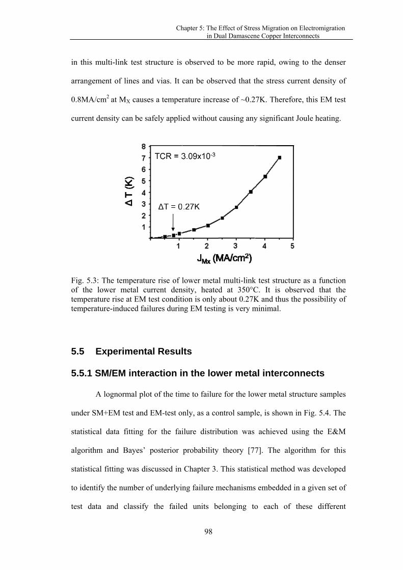
i
a
0
c
Fott
5
5
u
s
a
s
t
t
in this mult
arrangemen
0.8MA/cm2
current dens
Fig. 5.3: Thof the lowtemperaturetemperature
5.5 Exp
5.5.1 SM/
A lo
under SM+E
statistical d
algorithm a
statistical fit
to identify t
test data a
ti-link test s
nt of lines a
at MX caus
sity can be s
he temperatuwer metal ce rise at EMe-induced fa
periment
/EM inte
ognormal pl
EM test and
data fitting
and Bayes’
tting was d
he number
and classify
Ch
structure is
nd vias. It
ses a temper
safely appli
ure rise of lcurrent den
M test conditailures durin
tal Resul
raction i
ot of the tim
d EM-test o
for the fai
posterior
iscussed in
of underlyin
y the faile
hapter 5: The in Du
98
observed t
can be obse
rature incre
ied without
lower metansity, heatedtion is onlyng EM testin
lts
n the low
me to failure
nly, as a co
ilure distrib
probability
Chapter 3.
ng failure m
ed units be
Effect of Streual Damascen
to be more
erved that t
ease of ~0.2
causing any
l multi-linkd at 350°Cabout 0.27Kng is very m
wer meta
e for the low
ontrol sampl
bution was
theory [77
This statist
mechanisms
elonging to
ss Migration one Copper Inte
rapid, owin
the stress cu
27K. Theref
y significan
k test structuC. It is obK and thus tminimal.
al interco
wer metal s
le, is shown
achieved
7]. The alg
tical method
s embedded
o each of
on Electromigerconnects
ng to the d
urrent dens
fore, this EM
nt Joule heat
ure as a funbserved thathe possibil
onnects
structure sam
n in Fig. 5.4
using the E
gorithm for
d was deve
d in a given
these diff
gration
denser
ity of
M test
ting.
nction at the lity of
mples
4. The
E&M
r this
loped
set of
ferent

m
t
m
M
1
s
a
FoASf
mechanisms
test shows a
mechanisms
Mechanism
14.7% of th
sample (EM
are summar
Fig. 5.4: Faonly sampleAcceleratedSM+EM tesfor each sub
s. From the
a trimodal d
s. It is dedu
I (FM-I); t
he failures c
M-test only)
ized in Tab
ailure distribes for the std life tests st exhibits ab-population
Ch
e statistical
distribution
uced that 1
the majority
could be att
shows a mo
le 5.1.
bution of study of SMshow that
a trimodal dn of this mix
hapter 5: The in Du
99
study, the
, indicating
18.6% of th
y of the fail
tributed to F
onomodal d
amples undM/EM intera
the failuredistributionxture distrib
Effect of Streual Damascen
failure of t
g the presen
he test struc
lures (66.7%
FM-III. On
distribution
der SM+EMction in the
e distributio. The inset bution.
ss Migration one Copper Inte
the samples
nce of three
ctures failed
%) correspo
the other h
trend. The
M test compe lower meton of failedshows the r
on Electromigerconnects
s under SM
different fa
d due to Fa
ond to FM-I
hand, the co
statistical re
pared to EMtal interconnd samples uresistance t
gration
M+EM
failure
ailure
II and
ontrol
esults
M-test nects. under trends

Chapter 5: The Effect of Stress Migration on Electromigration in Dual Damascene Copper Interconnects
100
Table 5.1: Statistical test results for the MX test structure. Here, t50 is the measured median time to failure and σ is the standard deviation of the natural log of the failure times for each population of samples (also known as the lognormal shape parameter). The error estimates for t50 and σ were calculated with 90% two-sided confidence bounds.
Population t50
(Hours)
Confidence Bounds
(Hours) σ
Confidence Bounds
Lower
Bound
Upper
Bound
Lower
Bound
Upper
Bound
FM-I 42.27 40.6 44.0 0.05 0.027 0.086
FM-II 65.76 63.0 68.6 0.122 0.095 0.156
FM-III 117.44 98.5 140.1 0.211 0.113 0.372
Control 98.62 91.7 106.1 0.196 0.150 0.254
As evidenced by the FM-I and FM-II populations, when the SM effects in
the metal line are dominant, the EM median lifetime can be degraded by as much as
57.14% and 33.32%, respectively. This lifetime degradation suggests that SM can
potentially accelerate EM failures during circuit operation. On the other hand, the
statistical analysis also suggests that there is a small sub-population where the EM
lifetime is not greatly affected by SM, as observed for FM-III. Note that the higher
t50 for this sub-population compared to the control sample does not indicate that
there is any lifetime enhancement; it is just an artifact due to the small sample size.
The typical resistance trends for each group of failures are shown as an inset
in the plot below and in Appendix B. Both FM-I and FM-II groups of the SM+EM
samples show a catastrophic resistance shoot-up trend where open-circuit failures
occur abruptly. The FM-III group has a smaller resistance jump before the test was

Chapter 5: The Effect of Stress Migration on Electromigration in Dual Damascene Copper Interconnects
101
terminated. On the other hand, the resistance trend for the majority of the control
sample is a staircase-like gradually increasing trace which indicates that multiple,
small random voids in the via-chain structure nucleate and grow before a final
failure.
A PVC imaging technique was employed to locate the failure in the
multilink structures after the SM/EM test. Fig. 5.5(a) shows the TEM micrograph of
a device failed in the FM-I population which has an abrupt failure resistance trend.
It reveals that the void is formed exactly below the via at the M1 cathode side. The
TTF is very low because a small amount of Cu depletion around the via/metal
interface is sufficient to cause a large resistance change. Since FM-I and FM-II have
the same resistance characteristics, the voiding behavior of the FM-II population is
expected to be the same. On the other hand, in FM-III, the failures occurred at the
later stage where void forms in the trench of the metal line instead; as shown in Fig.
5.5(b). The TTF is enhanced because a large volume of Cu must be depleted prior
to reaching the resistance failure criteria. The cross-sections shown are direct
evidence that two very distinct failure modes are present.

Chapter 5: The Effect of Stress Migration on Electromigration in Dual Damascene Copper Interconnects
102
Fig. 5.5: Cross section of degraded sample after SM+EM test from (a) FM-I population, where the void formed directly below the via of the cathode end causing open circuit failure. (b) FM-III population, in which the trench void formed in the Cu metal line.
5.5.2 SM/EM interaction in the upper metal interconnects
The failure distribution of the samples under the SM+EM test and EM-only
test for upper metal structure is shown in Fig. 5.6. Statistical analysis indicated that
the failure of the samples under these two tests exhibits monomodal statistics. The
t50 for the upper metal structure under the EM-only test was 119.82-hours, which is
larger than the EM-t50 in the lower metal test structure. This experimental data is
consistent with the literature reports that the upper metal structure has a longer
lifetime since a larger void volume is required for open failure [63]. The t50 for the
samples under the SM+EM test was 107.55-hours, implying that the EM lifetime
degradation due to SM effect is ~10.24%. The statistical results are summarized in
Table 5.2.

Chapter 5: The Effect of Stress Migration on Electromigration in Dual Damascene Copper Interconnects
103
Table 5.2: Statistical test results for MX+1 test structure.
Population t50
(Hours)
Confidence Bounds
σ
Confidence Bounds
Lower
Bound
Upper
Bound
Lower
Bound
Upper
Bound
SM+EM Test 107.55 102.1 113.3 0.124 0.088 0.162
Control 119.82 113.1 126.9 0.154 0.115 0.195
The resistance evolution trends for all samples in both populations were
observed to be the same, i.e., a step-like resistance increase (see Fig. 5.6). In order
to assess void distribution in the multi-link test structure, a TIVA imaging technique
was used. As shown in Fig. 5.7, the bright spots show the void nucleation locations
in the via-chain structure on one of the degraded samples after the SM+EM test.
Some voids were detected at the end of the single-link metal line. There are two
possibilities of voiding site for the EM failure in the upper metal line, i.e., voiding
occurs inside the via or in the line [101]. When a void forms, spanning the via, all
the current must suddenly be carried by the highly resistive liner, thus causing a
sharp resistance increase by a rapid joule heating and ultimately a disruption of the
conduction path at a weak spot in the liner. On the other hand, when a void grows in
the line, the available Cu volume gradually decreases, and the current is gradually
shunted to longer sections of the liner, leading to a more gradual resistance increase.
Since all the samples have a step-like resistance increase behavior and we did not
observe any single sample having an abrupt resistance increase, voiding is most
likely believed to occur at the MX+1 trench.
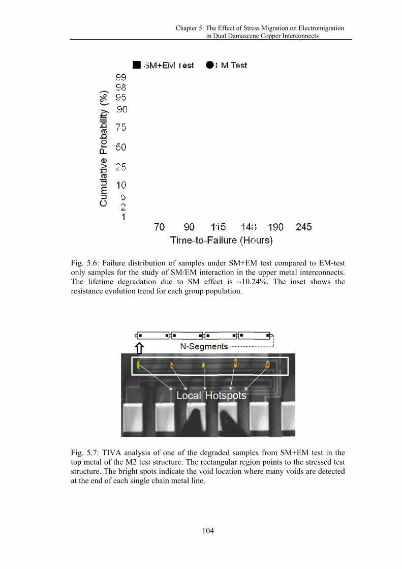
FoTr
Ftsa
Fig. 5.6: Faonly sampleThe lifetimresistance ev
Fig. 5.7: TItop metal ofstructure. That the end of
ailure distribes for the st
me degradatvolution tre
IVA analysif the M2 tehe bright spf each singl
Ch
bution of study of SMtion due toend for each
is of one ost structurepots indicatele chain met
hapter 5: The in Du
104
amples undM/EM intera
o SM effech group popu
f the degra. The rectane the void ltal line.
Effect of Streual Damascen
der SM+EMction in thect is ~10.2ulation.
ded samplengular regioocation whe
ss Migration one Copper Inte
M test compe upper met24%. The i
es from SMon points toere many vo
on Electromigerconnects
pared to EMtal interconninset show
M+EM test io the stresseoids are det
gration
M-test nects.
ws the
in the ed test tected

Chapter 5: The Effect of Stress Migration on Electromigration in Dual Damascene Copper Interconnects
105
5.6 Simulation
A finite element simulation code was developed to study the SM behavior
due to process-induced thermal stress profiles generated in the Cu/low-κ
interconnect structure and assess the most probable sites for vacancy accumulation.
The simulation model of the test structure shown in Fig. 5.2 was built using
ANSYS®. All these models were implemented assuming isotropic material
properties with linear elastic behaviors. Due to line symmetry, only a quarter of the
model was simulated. The material properties used are given in Table 5.3 and the
stress free temperature was set to 300°C. Simulations were performed at an SM-test
temperature of 200°C. In order to evaluate the validity of the simulation model
more quantitatively, the computed results have been compared with the data
obtained from volume-averaged thermal stress measurements in Cu using the XRD
technique as described in Ref. 24.
Table 5.3: Material properties used in our simulation model [15, 102].
Materials CTE (10-6/K) Modulus (GPa) Poisson’s Ratio
Cu 17.7 104.2 0.352
Ta 6.5 185.7 0.342
Si3N4 3.2 220.8 0.27
SICOH 12 16.2 0.3
Fig. 5.8 shows the simulated hydrostatic stress profile in the lower metal
lines of the Cu/low-κ interconnect system. It reveals that the region near the edge of
the metal bottom has the lowest tensile stress (~50MPa) and the highest tensile

Chapter 5: The Effect of Stress Migration on Electromigration in Dual Damascene Copper Interconnects
106
stress location is at the Cu bulk region (~185MPa). This generates a large stress
gradient between the Cu bulk and metal edge which enhances vacancy diffusion due
to thermo-mechanical stress of Cu interconnects. Furthermore, the insertion of a via
in the Cu metal lead enhances the non-uniform stress in the system. As reported in
Ref. [97], the thermally generated stress gradient in the Cu interconnect drives the
saturated vacancies from high stress regions towards low stress regions. Thus, the
non-uniform tensile stress near the via leads to a considerable stress gradient
causing the vacancies to be driven towards the via. The stress gradients along the
top interface of the metal line would favor an interface mechanism transporting
vacancies to the via edge, while the bottom-to-top stress gradient would favor a
grain boundary diffusion. Thus, grain boundaries might be an added feasible path
for more vacancies to contribute to the interface migration.
Fig. 5.8: FEA simulation of hydrostatic stress in the lower metal test structure. The non-uniform tensile stress near the via bottom leads to a prominent stress gradient that drives vacancies towards the via.

F
p
l
~
v
m
s
t
p
r
Fnvt
For
Fig. 5.9. An
peak stress g
lead (SM-I)
~135 MPa,
via ranges f
migrate tow
stress gradie
those vacan
process. Sin
region, mor
Fig. 5.9: FEnon-uniformvia (SM-II)these two di
upper meta
n interesting
gradient pre
) and inside
while at th
from ~30-13
wards these
ent, SM als
ncies within
nce ADV i
e vacancies
EA simulatiom tensile str. The resultifferent area
Ch
al lines, the
g feature in
esent in the
e the via (S
he edge, it i
35 MPa. Th
two differe
so depends
n this regio
in the SM-
s will be acc
on of hydroress is evideting stress as during SM
hapter 5: The in Du
107
e simulated
n this simul
two region
SM-II). The
s ~72 MPa
he resulting
ent areas du
on the activ
on would b
I region is
cumulated a
ostatic stresent near the gradient maM test.
Effect of Streual Damascen
hydrostatic
lation resul
ns, i.e., near
e hydrostati
. The non-u
stress grad
uring SM tes
ve diffusion
be able to
much larg
at the SM-I
s in the uppupper metaay favor va
ss Migration one Copper Inte
c stress pro
lt lies in the
the edge of
c stress at M
uniform ten
dient may fa
st. Howeve
n volume as
participate
ger compare
site.
per metal teal lead (SM-acancies to
on Electromigerconnects
ofile is show
e location o
f the upper
MX+1 Cu bu
nsile stress i
avor vacanc
r, apart from
s well [23].
e in the vo
ed to the S
est structure-I) and insidmigrate tow
gration
wn in
of the
metal
ulk is
in the
cies to
m the
Only
oiding
SM-II
e. The de the wards

Chapter 5: The Effect of Stress Migration on Electromigration in Dual Damascene Copper Interconnects
108
5.7 Proposed Failure Mechanism
From the electrical results, physical failure defect signatures and simulation
results, it is believed that during the SM test, the thermally generated stress gradient
in the Cu interconnect drives the saturated vacancies to diffuse towards the “weak”
via(s) as deduced from Figs. 5.8 and 5.9. A more compressive stress develops in
volumes in which atoms accumulate, whereas the stress becomes more tensile in
volumes in which atoms are depleted. The relative change in the atom concentration
( /C C ) corresponds to a change in the hydrostatic stress [45]
C
C B
where B is the effective modulus of the dielectric. Therefore, the metal lines near
the via become more tensile (σSM) after SM test due to vacancy accumulation. If
failure occurs when a critical stress (σcrit) is reached [45], this SM effect shortens
the nucleation time (tnucl) for the cathode. Hence, the equation for time to
nucleation, proposed by Korhonen et al. [45] can be rewritten as
2
2crit SM
nucltG
where G=Eq*/Ω, κ=DBΩ/kT, E is the electric field, ∆σ = σcrit – σSM is the marginal
additional stress needed to nucleate the void during EM test and q* is the absolute
value of the effective charge. Once a void is nucleated, it can evolve until it reaches
a critical void size which causes a significant resistance increase (Vfail). The
approximate growth time to reach the critical volume size is given by [13]
(Eq. 5.3)
(Eq. 5.4)

Chapter 5: The Effect of Stress Migration on Electromigration in Dual Damascene Copper Interconnects
109
failgrow
EM d
Vt
J A
where JEM is the atomic or vacancy flux driven by electromigration and Ad is the
effective cross-sectional area of the diffusion flux. The failure time can be
expressed as the sum of the time required to nucleate a void, tnucl, and the time it
takes for the void to grow and reach a certain resistance failure criterion, tgrow [16].
Substituting Eqs. (5.4) and (5.5), the failure time is expressed as
tfailure = tnucl + tgrow
2
2failcrit SM
failureEM d
Vt
G J A
It was observed that in the lower metal line structure, SM can severely affect
the EM lifetime as indicated by the FM-I (~57.1% degradation) and FM-II
population (~33.3% degradation) in Fig. 5.4. The EM lifetime degradation
mechanism is explained as follows - assuming a symmetrical condition, where the
amount of vacancies accumulated near the vias after the SM test are the same, the
metal line becomes more tensile at both ends by almost the same increment (σSM1
and σSM2), as illustrated in Fig. 5.10. Equation (5.5) indicates that when SM is
dominant, this tensile stress (σSM) shortens the nucleation time (tnucl) for the cathode
end during the EM test. It may cause void nucleation, if the stress developed at the
cathode region due to SM reaches the critical stress value (σSM → σcrit). This void
which functions as a sink of ensuing vacancies supplied by EM, continues to grow
until it reaches a critical void size which causes a significant resistance increase
(Eq. 5.5)
(Eq. 5.6a)
(Eq. 5.6b)

Chapter 5: The Effect of Stress Migration on Electromigration in Dual Damascene Copper Interconnects
110
(tgrow). On the other hand, at the anode side, the EM mass flux will cancel out the
vacancy accumulation. Therefore, the stress will be neutralized and during
subsequent EM stressing, this region progressively shows compressive stress due to
Cu atom accumulation. Our TEM analysis further supports this hypothesis. As
shown in Fig. 5.5(a), the induced void for a majority of the SM+EM test samples
was formed beneath the via, causing open circuit failure. This suggests that high
concentration of vacancies beneath the via after SM test, favors void nucleation in
this region during the EM test.
Fig. 5.10: Mechanism of SM and EM interaction – an approach using stress evolution diagram. (a) Schematic showing the atom and vacancy movements, assuming symmetrical structure condition, wherein the vacancy distribution near both ends after the SM stress test is assumed to be the same. (b) As a result, the metal line becomes more tensile by almost the same increment (σSM1 and σSM2) and the time to void nucleation is shorter, tN2 < tN1, during subsequent EM test at the cathode end.

Chapter 5: The Effect of Stress Migration on Electromigration in Dual Damascene Copper Interconnects
111
Since self-diffusion of vacancies in the polycrystalline microstructure
material during SM test is a random process, the amount of vacancies accumulated
near the vias at both ends after SM test can be largely different for a statistically
small subset of the samples tested. This could be the reason why we observe three
different populations for the samples under the SM+EM test. It may also be possible
to observe void nucleation prior to any EM test, if the stress developed at the
cathode region during SM reaches the critical value, σSM → σcrit. In this case, there is
no initial time required for void nucleation and the EM failure time is solely
governed by the growth time only, as shown in Equation (5.7).
( )fail
F GSM EM d
Vt t
J J A
On the other hand, the statistical results in Fig. 5.4 show a small late-failure
population where the EM lifetime is not degraded due to SM effect, i.e., the FM-III
group. The insensitivity to the SM effect for this sub-population may be attributed
to the possibility of “limited” vacancy density accumulation at the cathode region in
each single link of a serial chain test structure, compared to the anode region (see
Fig. 5.11), thereby making the resulting SM effect negligible. Equation (5.4)
indicates that when the SM effect is insignificant, the void is nucleated due to EM
flux only. The physical failure analysis for this failure mode shows that the void
occurs in the trench of the metal line and this failure is typical of EM downstream
failures as reported in Refs. [69, 103]. This observation agrees well with the in-situ
SEM analysis, where, in the case of the EM-only test, voids are formed at interfaces
(Eq. 5.7)

Chapter 5: The Effect of Stress Migration on Electromigration in Dual Damascene Copper Interconnects
112
and grain boundaries, often far away from the vias [104]. Depending on the
interface strength, voids can move over large distances in the opposite direction of
current flow.
Fig. 5.11: (a) Schematic showing the atom and vacancy movements, assuming the amount of vacancies at the cathode region is limited. (b) As a result, there is no tensile stress developed at the cathode side of the metal line after SM test. The time to reach void nucleation is the same, tN2 ≈ tN1, during EM test, i.e., SM effect is almost negligible.
Our observation that SM effects may accelerate EM failure kinetics agrees
well with the observation by M. Hauschildt et al. [105]. Their paper presented the
downstream EM failure distribution of samples under various stress temperatures,
ranging from 150ºC-325ºC. It was observed that the EM failure distribution of
samples subjected to SM-dominant temperatures, i.e., around 150 and 175ºC,

Chapter 5: The Effect of Stress Migration on Electromigration in Dual Damascene Copper Interconnects
113
showed a bimodal trend, whereas other temperature conditions exhibited
monomodal statistics (Fig. 5.12). A few very early failures were found at 150 and
175°C possibly indicating that the presence of SM can accelerate the EM failure
process, resulting in a much shorter time to failure.
Fig. 5.12: Logormal EM failure distribution of lower metal interconnect samples under various stress temperatures, ranging from 150ºC-325ºC [105].
In the case of the upper metal structure, Fig. 5.5 shows that the group of
samples under the SM+EM test suffers ~10.2% degradation. From the initial
resistance data prior to the EM test, there was no classical SM failure detected in
any of the samples since there were no abrupt failures. The literature suggests that
SM voiding in upstream structure is typically located inside the vias, causing open
circuit failure [35, 89].
very early failures

Chapter 5: The Effect of Stress Migration on Electromigration in Dual Damascene Copper Interconnects
114
From the experimental and simulation results above, we postulate that SM
can potentially accelerate EM failures at nominal circuit operating conditions
because of vacancy accumulation at the end of the metal line and shorten the
nucleation time (tnucl) for the cathode end to reach the critical voiding stress during
the EM test earlier. SM stress can shorten the time to reach nucleation stress during
EM test, as shown in Eq. 5.6. However EM degradation in the upper metal structure
is not as severe as in the lower metal structure because after a void has nucleated at
the Cu/Si3N4 interface of the MX+1 structure, the void still needs a long time to grow
to span the whole thickness of the metal line before it causes resistance of the line to
increase substantially. This suggests that for upper metal structures, the nucleation
time is negligible compared to void growth time, i.e., tnucl < tgrow. In such a case, it is
the growth process, not nucleation that causes the device to fail most of the time. In
contrast, for the MX test structure, voids will preferentially nucleate near the
cathode end of the Mx bottom via. Thus, the amount of growth in void size needed
to cause failure in Mx is much lower.
The effect of SM on EM is more prominent when the technology node is
scaled down to the sub-45nm range. Smaller vias need a lower vacancy density to
cause the metal line to reach the required critical tensile stress for void nucleation.
In addition, the introduction of more porous low-κ materials lowers the critical
nucleation stress [44]. This will reduce the time-to-failure for the cathode end to
reach a vacancy threshold for super-saturation which, in turn, leads to a much
earlier void nucleation at the interface. However, this SM and EM interaction could
be minimized with some process improvement, such as optimizing post-plating
annealing conditions. Equation 5.2 indicates that the atomic flux in BEOL is a

Chapter 5: The Effect of Stress Migration on Electromigration in Dual Damascene Copper Interconnects
115
function of the hydrostatic stress gradient. Therefore, reducing post-plating
annealing temperature will reduce SFT, leading to lower stress gradients. Reference
[106] reported that long low-temperature post-plating annealing has a superior SM
and EM performance compared to long high-temperature post-plating anneal.
5.8 Summary
In this chapter, we have studied the interaction of SM and EM in the lower
and an upper metal leads of dual-damascene Cu/low-κ interconnects. The
dependency and combined effect of these two key failure mechanisms are important
to be understood, as it is expected to be dominant in the chip when used at nominal
operating conditions, wherein the thermal hydrostatic stresses are considerably
higher. The typical accelerated EM testing conditions are at a relatively high
temperature, typically close to the SFT of the metal lines. As a result, the effect of
intrinsic thermal stress on the reliability and lifetime of metal lines is seldom
properly accounted for and the current reliability projections based on the standard
EM test algorithms may be overly optimistic.
The influence of the SM on EM behavior in Cu interconnects was analyzed
here from a statistical, electrical and physical perspective. The results from these
different types of analysis clearly reveal that the EM failure time of the metal line
could be strongly affected by the presence of the residual stresses, due to SM at the
cathode end. When the SM effect in the lower metal line is dominant, the EM
lifetime could be degraded by as much as 30 – 60%. TEM analysis shows that the
void tends to nucleate and grow beneath the via, causing catastrophic failure. This
phenomenon is attributed to vacancy accumulation near the vias after the SM test,

Chapter 5: The Effect of Stress Migration on Electromigration in Dual Damascene Copper Interconnects
116
causing the metal line to become more tensile and thereby shortening the nucleation
time (tnucl) for the cathode end to reach σcrit during the EM test. However, vacancy
diffusion in the polycrystalline material during SM test is expected to be a random
process. When vacancy accumulation at the cathode region is limited, the SM effect
may be negligible and EM lifetime is not degraded, which is shown by the small
late-failure population in the statistical plot of Fig. 5.4.
For the upper metal structure, the failure distribution of samples under the
SM+EM test shows that the EM lifetime was degraded by ~10%. It was observed
that the EM degradation is not as severe as in the case of the lower metal line.
Unlike in the lower metal structure, after a void has nucleated at the Cu/Si3N4
interface of the MX+1 structure, the void still needs to grow to span the whole
thickness of the metal line before it causes the resistance of the line to fail.. Since
the lower metal structure has a poorer EM lifetime compared to the upper metal
structure and the EM degradation due to SM was observed to be more significant in
MX, we may conclude that the lower metal structure is the weakest link determining
the overall back-end chip lifetime.

Chapter 6: The Influence of Stress Migration on Electromigration Parameters in Dual Damascene Copper Interconnects
117
CHAPTER 6
THE INFLUENCE OF STRESS MIGRATION ON
ELECTROMIGRATION PARAMETERS IN COPPER
DUAL DAMASCENE INTERCONNECTS
6.1 Introduction
The estimation of device lifetime at normal operating conditions is obtained
from the extrapolation of accelerated failure test data. For Cu interconnects, the
most common industrial practice to predict its lifetime is to extrapolate the EM
reliability test to operating conditions using Black’s equation:
expn aETTF Aj
kT
where A is an empirically determined constant, j is the current density, n is the
current density exponent typically ranging between 1 and 2, and Ea is the activation
energy. It has been established through previous studies that a value of n=1
corresponds to the void-growth-limited EM failure, while void-nucleation-limited
failure is represented by n=2 [16].
One of the limitations of the extrapolation method using Black’s equation is
that it does not consider the effect of intrinsic thermal stress (SM). On the other
hand, as discussed in Chapter 3,the lifetime extrapolation based on an accelerated
SM-only test for Cu interconnect is not feasible considering the very long test
durations needed. The small amount of data that can be collected limits the failure
distribution characterization and failure rate projection to use condition.
Eq. (6.1)

Chapter 6: The Influence of Stress Migration on Electromigration Parameters in Dual Damascene Copper Interconnects
118
Eq. 6.1 shows that there are two important parameters for interconnect
lifetime extrapolation, i.e., activation energy and current density exponent.
Therefore, in this chapter, we will characterize the effect of SM on these two EM
parameters. After that, a simple empirical method to extrapolate the interconnect
lifetime accounting for the effect of both SM and EM will be discussed. Finally, the
influence of SM on other important EM parameters, i.e., permittivity scaling and
short length effect, will be investigated as it is important for the assessment of
further technology scaling and interconnect design.
6.2 Experiment
The test structure design is basically similar with the previous experiment
(Chapter 5). However, in this test, we investigated two different ILD materials, i.e.,
SiCOH, with κ~3, and FTEOS, with κ~3.7, for assessing the permittivity scaling
effect. The length of MX was shortened to 10μm and 40μm for the short length
experiment. All the SM/EM tests were carried out at the package level. Firstly, the
samples were subjected to SM stress through a thermal bake at 200°C for 1000
hours. Immediately after the SM stress, the samples were transferred from an oven
to an EM tester with a temperature of 350ºC. The failure criterion used was the first
abrupt jump in resistance.
6.3 Characterization of Activation Energy
The activation energy represents the energy barrier against the diffusive
process resulting in EM and has an exponential relationship with EM lifetime so
that increase in Ea is highly desirable [39]. It has been shown that the numerical

Chapter 6: The Influence of Stress Migration on Electromigration Parameters in Dual Damascene Copper Interconnects
119
value of Ea is representative of different specific diffusion paths. The possible
diffusion paths in the Cu damascene line are grain boundaries, the Cu/dielectric
interface and the Cu bulk with a range of activation energies as 1.2eV, 0.7-1.0eV,
and 2.3eV, respectively [98]. For EM, it is well known that the main diffusion path
in Cu lines is along the Cu/cap interface. On the other hand, the dominant diffusion
mechanisms for SM is interfacial and grain boundary diffusion [23]. The voids are
expected to be formed by agglomeration of vacancies at interfaces and grain
boundaries within an active diffusion volume, which is the contour region within
which vacancies are able to participate in the voiding process.
The effect of SM on EM activation energy was examined here with stressing
the samples at three different EM temperatures, in the range of 300 to 350°C,
maintaining the current density stress at 0.8 MA/cm2. The lognormal plot of the
TTF for the samples under SM+EM test and EM test-only for lower metal structure,
at 300 and 325°C, is shown in Fig. 6.1, while the failure distribution at 350°C has
been shown earlier in chapter 5. The t50 and shape parameter (σ) values of the
lifetime distributions are consistent, where the t50 is increasing as the temperature
decreases and sigma values are comparable over the entire temperature range.
Statistical analysis indicates that the failure of the samples which has been subjected
to SM test exhibits bimodal distributions, independent of the EM test temperature.
The early failure population which shows lifetime degradation suggests that SM can
potentially accelerate EM failures during circuit operation (FM-A). While the other
population shows that the EM lifetime is not greatly affected by SM (FM-B). The
t50 of FM-B population is found to last about 30-40% longer than the FM-A
population with a similar σ value at the various test temperatures.

Chapter 6: The Influence of Stress Migration on Electromigration Parameters in Dual Damascene Copper Interconnects
120
Fig.6.1: EM lognormal failure distribution of SM+EM test and EM-test only samples at test temperatures of T = (300, 325)°C.
The activation energy of FM-A population was extracted to determine the
dominating diffusion mechanism for samples which are affected by SM. From the
slope of t50 versus temperature (Fig. 6.2), it can be deduced that the activation
energy of FM-A samples and control samples are 0.71eV and 0.79eV, respectively.
Both these values represent diffusion at the Cu/Si3N4 interface of the MX line, in
good agreement with data reported in literature [98]. This result suggests that there
is no change in the dominant diffusion mechanism for the sample which has been
subjected to the additional SM stress.
Figure 6.3 illustrates the void formation process during SM+EM test. In the
SM test, thermally generated stress gradients in the Cu interconnect drive the
saturated vacancies to diffuse towards the via. As a result, the vacancies will
accumulate in the interface and the grain boundary region near the vias. However,
since the EM diffusion path is predominant at the interface, our experimental result
suggests that only vacancies generated at the surface can contribute to the void
FM-A
FM-B

Chapter 6: The Influence of Stress Migration on Electromigration Parameters in Dual Damascene Copper Interconnects
121
formation process during EM.
Fig. 6.2: Plot of ln(t50) versus (1/kT) with extracted values of EM activation energy for lower metal structure. It shows that both values represent diffusion at the Cu/cap interface.
Fig. 6.3: The possible mechanism of SM and EM interaction. It shows that after SM test, vacancies will be accumulated both at the interface and grain boundaries of the metal lead near the vias. However, since the main diffusion path for subsequent EM is along the Cu/cap interface, only vacancies in the surface would be able to contribute to the void nucleation process.
The effect of SM on EM activation energy for upper metal structure is
examined as well. From the slope of t50 versus temperature (Fig. 6.4), it can be
deduced that the Ea value of SM+EM samples and control samples are 0.929eV and
0.933eV, respectively. Again, both these values are representative of diffusion
along the Cu/ Si3N4 interface of the MX+1 line. This suggests that there is no change
in the dominant diffusion mechanism for the upper metal line.

Chapter 6: The Influence of Stress Migration on Electromigration Parameters in Dual Damascene Copper Interconnects
122
Fig. 6.4: Plot of ln(t50) versus (1/kT) with extracted values of EM activation energy for the upper metal structure. It can be inferred from the data that the similar value of Ea ~ 0.93eV represents diffusion at the Cu/cap interface for both tests.
6.4 Characterization of Current Density Exponent
In this part, the influence of SM on the EM current density exponent is
investigated. The samples were stressed at three different EM current densities,
ranging from 0.6MA/cm2 to 1 MA/cm2 with T = 350°C. A lognormal plot of the
TTF for the samples under SM+EM test and EM-test only for upper metal structure
is shown in Fig. 6.5. The EM median lifetime is extracted and plotted against the
applied current density (Fig. 6.6). From the slope of this plot, the current density
exponent can be obtained, in which the n value of SM+EM stressed samples and
control samples are 2.071 and 1.796, respectively.
A similar method was applied to the lower metal structure, and from the
slope of t50 versus applied current density (see Fig. 6.7), it can be deduced that the
current density exponent in Black’s equation for the SM+EM stressed samples and
EM test-only are 1.76 and 1.88, respectively. These results suggest that void has not
been nucleated before EM test.

Chapter 6: The Influence of Stress Migration on Electromigration Parameters in Dual Damascene Copper Interconnects
123
Fig.6.5: Lognormal failure distribution for samples under SM+EM test compared to EM-test only samples at T = (300, 325)°C. Accelerated life tests show that the TTF of samples with SM+EM test show significant lifetime degradation by ~10%.
Fig.6.6: Plot of ln(t50) versus ln(1/J) with extracted values of Cu migration activation for SM+EM test and EM test-only samples in the upper metal line. The data indicates that there is no drastic change of the “n” value for samples which were subjected to additional SM stress.[107]

Chapter 6: The Influence of Stress Migration on Electromigration Parameters in Dual Damascene Copper Interconnects
124
Fig.6.7: Plot of ln(t50) versus ln(1/J) with extracted values of Cu migration activation energy for SM+EM test and EM test-only samples in the lower metal line. Again, no significant change in the “n” value is observed for samples which had been subjected to additional SM stress.
The observation of a relatively constant Ea and n values for the SM+EM and
EM-only stressed samples suggests that the failure mechanism of these two samples
has to be similar. Therefore, we can validate the use of the Black’s equation for
SM+EM stress case to extrapolate the failure time obtained from accelerated test
conditions to operating conditions. Since the SM+EM stressed samples have a
shorter lifetime than the EM-test only samples, extrapolating the EM-only test
results of lifetime may be too optimistic to predict the overall interconnect
reliability. In order to be more conservative in predicting the interconnect lifetime,
it is necessary to introduce a proportionality constant, the EM accelerating factor
(AF), which describes the effect of SM in reducing the lifetime. The AF can be
expressed as:
50
50
SM EM
EM
tAF
t
(Eq. 6.2)

Chapter 6: The Influence of Stress Migration on Electromigration Parameters in Dual Damascene Copper Interconnects
125
Using the Black’s equation, we can re-express the interconnect lifetime operating
condition, which incorporates the effect of SM on EM, as:
1 1exp
n
strop str
op op str
a
B
jTTF TTFj T T
EAFk
where TTFop is the extrapolated failure times at operating condition, TTFstr is the
EM accelerated failure time, jstr and jop are the current densities at stress and
operating condition and (Tstr, Top) are the temperatures at stress and operating
condition.
6.5 Dielectric Permittivity Scaling Effect
The drive towards increased device density and improved performance in
semiconductor devices makes the switch from SiO2 to low-κ materials ILD
inevitable. Transition to lower-κ materials is necessary to prevent crosstalk between
conducting lines and reduce signal delays in the BEOL interconnect wiring. As
shown in Fig. 6.8, in general, the ILD material generations can be classified into
three groups, i.e., ILD materials with dielectric constants κ > 3.0 (group I), κ = 2.5
to 3.0 (group II), and κ < 2.5 (group III). In this part, we assess the SM and EM
interaction for two different ILD groups, i.e., group I and II. The materials chosen
for integration with copper are FTEOS (κ ~ 3.7) and low-κ material - SiCOH (κ ~
3.0).
Figure 6.9 shows the failure distribution for samples under SM+EM test
compared to EM-test only samples. Accelerated life tests show that no degradation
occurs for Cu interconnects with FTEOS dielectric. On the other hand, the effect of
(Eq. 6.3)

S
m
Fom
Fowfa
SM and EM
materials.
Fig. 6.8: Peobtained fromodulus als
Fig. 6.9: Faof EM-test with low-κ dfailure timeaffected by
M interaction
rmittivity vom Refs. [1so decreases
ailure distribonly. Acceldielectric exes for the the SM-EM
Chapt
n seems to
value vs. ela4, 15, 24,
s.
bution for slerated life xhibit signitest structu
M interaction
ter 6: The Infl Paramet
126
be quite de
astic modulu102, 108] A
samples untests show ficant lifetim
ure with con.
luence of Streters in Dual D
etrimental w
us for commAs the value
der SM+EMthat the TT
me degradaonventional
ess Migration Damascene Co
with the inte
monly availe of κ decre
M test compTF of SM+Eation. On the
FTEOS di
on Electromigopper Intercon
egration of l
lable low-κeases, the e
pared to theEM test same other hanielectric ar
gration nnects
low-κ
κ ILD, elastic
e case mples d, the e not

Chapter 6: The Influence of Stress Migration on Electromigration Parameters in Dual Damascene Copper Interconnects
127
To understand the mechanism, we developed an FEA simulation code. We
compared the hydrostatic stress at this interface for different dielectric materials
with κ = 3.7 (FTEOS), 3.0 (SICOH) and 2.1 (p-SICOH), which represents a normal
low-κ and ultra low-κ ILD material, respectively. The same material properties,
shown in table 5.3, are used for simulation in Figs.6.10 and 6.11. The material
properties of FTEOS and p-SICOH dielectrics are shown in Table 6.1.
Table 6.1: Material properties used in our simulation model [15,102]
Materials CTE (10-6/K) Modulus (GPa) Poisson’s Ratio
FTEOS 1 59 0.16
p-SICOH 16 3.85 0.28
Figure 6.10 shows the normalized hydrostatic stress as a function of distance
along the Cu/cap interface and Fig. 6.11 shows the stress profile at a depth of 30nm
from the interface. It shows a steep stress gradient from point A to B for Cu with
low-κ material, while the stress gradient for FTEOS dielectric is almost flat. This
suggests that the integration of low-κ materials favors self diffusion of vacancies
along the interface towards the via (SM phenomenon) due to the stress gradient
driving force. Hence, when the electron flows from via to lower metal, the EM flux
will interact with the vacancies accumulation caused by SM, leading to early
failures.
For future implementation of low-κ materials in the sub-45 nm technology
node, our simulation results show that for further lowering of κ values in the back-
end dielectric structure beyond κ ~ 3, there is no further rise in the stress gradients.
This means that the rate of vacancy diffusion towards the via is the same for lower-

Chapter 6: The Influence of Stress Migration on Electromigration Parameters in Dual Damascene Copper Interconnects
128
κ materials. However, as the critical stress (σcrit) for void nucleation decreases when
the Young’s modulus of the inter-level dielectric decreases, the implementation of
lower-κ dielectrics becomes a big challenge. The critical stress can be approximated
by [44]:
crit B
where B is the effective bulk modulus and γ is the interface energy per unit area. As
the critical stress goes down, the time-to-failure for the cathode end to reach a
vacancy threshold for super-saturation decreases as well, leading to a much earlier
void nucleation at the interface.
Fig. 6.10: The hydrostatic stress value (normalized) of lower metal structure, obtained from finite element simulation, as a function of distance at the Cu/cap interface.
(Eq. 6.4)

Chapter 6: The Influence of Stress Migration on Electromigration Parameters in Dual Damascene Copper Interconnects
129
Fig. 6.11: The hydrostatic stress value (normalized) of lower metal structure, obtained from finite element simulation, as a function of distance at the at a depth of 30nm from Cu/cap interface.
6.5 Short Length Effect
The EM threshold or short-length or Blech effect has been observed in the
interconnect line for over 30 years [41]. It was found that shorter interconnect
lengths are significantly less susceptible to EM damage than longer ones under the
same stressing conditions. Because of this favorable condition, the short-length
effect has been incorporated into circuit designs to allow for increased current
densities at short conductor lengths [109].
Basically, the short-length effect phenomenon is caused due to the EM-
induced mechanical stress gradient that generates a back flow of metal atoms in the
direction opposite to the EM flux. The EM flux transports metal atoms toward the
anode causing accumulation. This accumulation increases the chemical potential to
such a level that further transport of the atoms to the anode is slowed down or even

Chapter 6: The Influence of Stress Migration on Electromigration Parameters in Dual Damascene Copper Interconnects
130
impossible. As a result, the EM lifetime increases or may even reach immortality
condition, if the accumulation induced back-stress from the anode end balances the
electron wind force (see Fig. 2.12).
However, it is to be noted that most previous studies investigated the short-
length effect phenomenon under EM-test only. As we might find SM and EM co-
existing at operating conditions, it is important to investigate the SM and EM
interaction and Blech effect in a short line structure. The immortality condition of
short interconnect lines with respect to EM-only does not mean that the line would
not fail at use condition. As previously discussed, the atomic flux in the BEOL
interconnects at use condition can be expressed by Eq. 6.5. The interaction among
the mechanical stress gradient (term 1), electron wind force (term 2), and the back
stress gradient (term 3) needs to be fundamentally understood.
aSM EM
B
DCJ F F
k T
*a mech a a EW
B B B
DC DC DCJ Z e j
k T x k T k T x
Here the terms 1, 2 and 3 describe the influence of the mechanical stress gradient,
electrical current and back-stress, respectively.
The focus of our study is only for lower metal line, with the length of M1
being L = 10μm and 40μm. The effect of SM was introduced to the samples with
stressing them at a thermal bake of 200°C for 1000-hours. After that, the samples
were subjected to EM stress, with three different levels of (jL) product, i.e., (jL) <
(jL)c, (jL) ≈ (jL)c, and (jL) > (jL)c. The dielectric used in this work is SiCOH with
(Eq. 6.5)
term 1 term 2 term 3

Chapter 6: The Influence of Stress Migration on Electromigration Parameters in Dual Damascene Copper Interconnects
131
κ~3.0, and it has been reported that the (jL)c for downstream stressing with this
dielectric material is 2100 A/cm [42]. In this experiment, we limited the EM
stressing time to 200-hours. Therefore, if the samples did not fail or show sufficient
degradation within this period of time, it was considered to be immortal.
The first stressing condition is at j=1MA/cm2 corresponding to
(jL)=1000A/cm, such that (jL) < (jL)c. As shown in Fig. 6.11, if the stressing
condition is much lower than the threshold criterion, there is no substantial
resistance degradation, which implies immortal behavior for both SM+EM test and
EM-only test samples under these conditions. The small resistance increase, around
3-4%, is a typical behavior observed during short-length test [109, 110]. This
saturation of the resistance increase with time indicates the suppression of further
EM-induced damage [109]. However, this immortality condition does not mean that
the line would not fail at use condition. The literature reports have shown that the
line can still fail due to SM effect, independent of the length. SM failures have been
observed at various interconnect lengths of L = 1.5 μm, 30 μm and 70 μm (Fig.
6.13).
(a)

Chapter 6: The Influence of Stress Migration on Electromigration Parameters in Dual Damascene Copper Interconnects
132
Fig. 6.12: Resistance change versus time during EM stress for (a) EM test-only and (b) SM+EM test samples, with electrical stress duration fixed to 200 hours. The resistance change for both samples is small, around 3-4% and tends to eventually saturate, which is representative of the immortal behavior.
Fig. 6.13: SM failure at various interconnect lengths, (a) L=1.5μm [23], (b) L=30μm [95] and (c) L=70μm [92]. Void nucleation and subsequent growth occurs due to SM flux, independent of the metal length.
The second stressing condition is at 2MA/cm2 where in (jL)=2000A/cm,
such that (jL)≈(jL)c. As shown in Fig. 6.14(a), the resistance evolution trend of EM
test at this stress condition still shows an immortal behavior up to 200 hours of
(b)
(b)
(a)
(c)

Chapter 6: The Influence of Stress Migration on Electromigration Parameters in Dual Damascene Copper Interconnects
133
testing. However, when the EM test is performed on SM+EM test samples, a subset
of the population starts to fail (Fig. 6.14(b)). For the 18 samples tested, 11 samples
(61%) failed within the stress time. This set of results suggest that if the SM
residual stress is very high, the line still fail EM, even if the (jL) product is ≤ (jL)c.
This shows that the immortality condition in the short length structures may no
longer hold true if the tensile stress built-up due to SM (σSM) and EM (σEM) is larger
than the back-stress, that pushes the ions in the opposite direction. On the other
hand, for a long line, the situation can be even worse since the high residual stress
will accelerate EM failure as discussed previously in Chapter 5.
Fig. 6.14: Resistance evolution with time in (a) EM test-only and (b) SM+EM test samples, for 200 hours of EM testing. The resistance change for EM-test only samples is small, which shows the immortality behavior. On the other hand, for SM+EM test samples, the voids start to nucleate and saturate, with 61% of the lines failing.
(a)
(b)

Chapter 6: The Influence of Stress Migration on Electromigration Parameters in Dual Damascene Copper Interconnects
134
The last stressing condition is at j=1MA/cm2, tested with a similar test
structure, but a longer line L = 40μm, so that (jL)=4000A/cm > (jL)c. As shown in
Fig. 6.15, for EM-test only samples, when the back-stress disappears, the void
nucleates within a much shorter time (10 hours), and then it grows very rapidly
prior to open circuit failure. We can expect the failure times to be further shortened
if these samples were subjected to the SM+EM test routine.
Fig. 6.15: Resistance evolution with time in fresh samples (non-SM stressed) for 200 hours of EM testing. The stressing condition is at j=1MA/cm2, tested with a longer line metal, L = 40μm. Since (jL) > (jL)c for this case, the void is observed to nucleate and grow very rapidly.
6.6 Summary
We have presented a detailed characterization study of the SM effect on EM
degradation parameters, i.e., activation energy, current density exponent, dielectric
permittivity and short length effects, as it is important for lifetime extrapolation,
assessment of further technology scaling feasibility and exploration of alternative
interconnect designs. It was found that samples which were subjected to SM stress
have Ea=0.71eV and n=1.76, almost similar to that of the control samples -

Chapter 6: The Influence of Stress Migration on Electromigration Parameters in Dual Damascene Copper Interconnects
135
Ea=0.79eV and n=1.88, for the lower metal line structure. Correspondingly, the Ea
and n values for the upper metal structure for SM+EM test sample and EM-test only
samples are Ea=0.929 and 0.937eV and n=1.8 and 2, respectively. These activation
energy values represent diffusion at the Cu/cap top interface of the metal line. There
is no change in the dominant diffusion mechanism for the samples which have been
subjected to additional SM stress.
The observation of a relatively constant Ea and n value for the SM+EM
stressed samples and EM-only samples suggest that the failure mechanism for these
two test conditions is similar. Therefore, we consider it to be valid to still use the
Black’s equation to extrapolate the failure time obtained from accelerated tests to
use condition. In order to include the impact of SM on the lifetime, we propose to
include the AF term which we define to be the ratio of (t50)SM+EM to (t50)EM.
The effect of SM on EM parameters was further investigated by
characterizing the interaction for different ILD materials. This study has far
reaching implications for the assessment of future interconnects technology scaling.
Accelerated life tests show that no degradation occurred for Cu interconnects with
FTEOS dielectric under SM+EM test. From the finite element simulation results,
we find interfacial hydrostatic stress gradients to be high for the case of low-κ
materials (κ < 3), making them more vulnerable to SM effect, as compared to
FTEOS.
Lastly, we studied the effect of SM on EM for short length metal lines, to
understand the interaction among mechanical stress gradient, electron wind force,
and the back stress gradient. We found that the immortal behavior of short length
interconnects may be non-existent if the stress built-up due to SM can interact with

Chapter 6: The Influence of Stress Migration on Electromigration Parameters in Dual Damascene Copper Interconnects
136
a sufficiently strong electron wind force to exceed the critical stress for void
saturation. This study clearly highlights the need for considering the multiple
dependent failure mechanisms and their associated driving forces while assessing
the overall reliability of any interconnect structure.

Chapter 7: Stress Migration Risk on Electromigration Reliability in Advanced Narrow Line Copper Interconnects
137
CHAPTER 7
STRESS MIGRATION RISK ON ELECTROMIGRATION
RELIABILITY IN ADVANCED NARROW LINE COPPER
INTERCONNECTS
7.1 Introduction
In this chapter, we extend our study on the area effect of SM on EM reliability
in Cu interconnects, to present a comprehensive investigation comparing wide and
narrow Cu line-width test structures. The focus of our study is only for lower metal
line, because as discussed in chapter 5, it is the weakest link determining the overall
back-end chip lifetime. In the first part of this work, we present the results of
experimental studies in the very fine lines, followed by the discussion on the
degradation mechanism. In the subsequent part, a method to estimate the EM void
nucleation and growth time using Monte Carlo simulation technique is discussed.
In recent years, SM is studied from the perspective of “stress gradient”, active
diffusion volume, vacancy flux and Cu grain boundary effects [23, 108, 111, 112].
Geometrical effects in terms of the width and length of the wide metal line are also
found to have a significant influence on SM [32, 95, 113]. It is reported that SM
failure is more rampant in wider metal lines because the larger metal plates serve as
a better vacancy reservoir within one diffusion length of the via. Voiding in narrow
lines appears to occur only at extremely long stressing time of 12,000 hours (>1
year) [113]. Therefore, the current understanding is that SM is a risk factor in large
metal plates and not so much of a critical concern for further downscaled structures.

Chapter 7: Stress Migration Risk on Electromigration Reliability in Advanced Narrow Line Copper Interconnects
138
The SM reliability of Cu interconnects for narrow line width structures is seldom
reported.
It is to be noted that most of the previous studies on SM failure are only based
on the void growth phenomenon, causing resistance increase of the metal lines,
which may gradually affect the functionality of the circuit. However, beside this SM
void-growth risk, the influence of SM on the EM reliability has to be considered
since SM and EM are expected to co-exist concurrently at normal operating
conditions. SM might be prevalent all the time when the chip is working, typically
at temperatures around 100-125°C. At the same time, EM failures can be triggered
by the electron wind force through the interconnect and further enhanced due to the
SM effect.
7.2 Experiment
The test structures design used in this study is basically similar with the
previous experiment, as discussed in Chapter 5. Figure 7.1 shows the schematic
diagram of the test structure used in this study, which consists of an arrangement of
serial interconnects. The cross sectional area of the test structures was 0.07×0.14
µm2 (width×height). The via diameter was 0.07 µm. The ILD material was a
carbon-doped oxide, SiCOH (κ~2.7).
All the SM/EM tests were carried out at the package level. Firstly, the
samples were subjected to SM stress through a thermal bake at 200°C for 1000
hours. Immediately after the SM stress, the samples were transferred from an oven
to an EM tester with a temperature of 300ºC and a stressing current of 0.8 MA/cm2.
The failure criterion used was the standard 10% increase in resistance.

Chapter 7: Stress Migration Risk on Electromigration Reliability in Advanced Narrow Line Copper Interconnects
139
Fig. 7.1: Schematic showing the basic unit of the via-chain test structure used for the SM-EM interaction study in the narrow lines. The width of both metal levels are 0.07 µm. By keeping the upper metal short, EM failure is induced in the lower metal line only.
7.3 Electrical Characterization
A lognormal plot of the failure times for the lower metal structure samples
under SM+EM test and EM test-only, as a control sample, is shown in Fig. 7.2. The
statistical data fitting for the failure distribution of both samples is best represented
by a monomodal distribution. The EM-t50 for the samples under the SM+EM test is
degraded by ~38% than the control sample (EM test-only), and the lognormal
failure distribution shows a shallower spread with shape parameter, σ, dropping
from 0.548 to 0.193. In order to confirm this electrical result, other narrow test
structures were also tested. The basic configuration is the same, but the metal cross
section area is slightly larger. The width × height of the metal lead is 0.14 × 0.25
µm2 and the via diameter is 0.14 µm. The ILD has a higher permittivity value of κ ~
3.0. As shown in Fig. 7.3, a similar trend was observed, where both samples showed
a monomodal trend and the t50 for the samples under SM+EM test was degraded by
~24%.

Chapter 7: Stress Migration Risk on Electromigration Reliability in Advanced Narrow Line Copper Interconnects
140
Fig. 7.2: Lognormal probability plot of time to failure for samples under SM+EM test compared to EM-test only samples for M1-structures with line-width = 0.07 µm, height=0.14µm encapsulated with a low-κ dielectric material (κ~2.7). Statistical fitting results indicate that the median time-to-failure for samples subjected to SM+EM is ~38% lower than that of the EM-only test samples.
Fig. 7.3: Lognormal probability plot of time to failure for samples under SM+EM test compared to EM-test only samples for M1-structures with line-width = 014 µm, height=0.25µm encapsulated with a low-κ dielectric material (κ~3.0). Statistical fitting results indicate that the median time-to-failure for samples subjected to SM+EM is ~24% lower than that of the EM-only test samples.

Chapter 7: Stress Migration Risk on Electromigration Reliability in Advanced Narrow Line Copper Interconnects
141
The effect of SM on EM was further examined by characterizing the current
density exponent of the Black’s equation (n). It has been established through
previous studies that the n value, which is obtained from the EM test, can be
correlated to the failure mechanism of the metal interconnects. In theory, a value of
n=1 corresponds to the void-growth-limited EM failure, while void-nucleation-
limited failure is represented by n=2 [16]. Interestingly, the experimental work
showed that a current density exponent value for samples under EM-test only often
falls in between 1 and 2, i.e., 1.3 – 1.7 [110, 114, 115]. This suggests that within a
set of data, there are sub-populations which undergo void-growth-limited and void-
nucleation-limited failures [110].
In this study, the samples which had been subjected to SM-test, were stressed
at three different EM current density values, jEM, ranging from 0.6 - 1 MA/cm2 with
T = 300°C. From the slope of the median lifetime versus current applied (see Fig.
7.4), it can be deduced that the current density exponent in Black’s equation for the
SM+EM stressed samples is ~1, which clearly indicates a void-growth limited
failure. As a result, we suspect that in SM+EM samples, the void has been
nucleated in the line prior to the EM test due to the SM effect, causing significant
EM lifetime degradation, resulting in a shallower distribution spread.

Chapter 7: Stress Migration Risk on Electromigration Reliability in Advanced Narrow Line Copper Interconnects
142
Fig. 7.4: Logarithmic plot of the variation of the median time to failure (t50) with inverse current density (1/J). The linear fit to the data on this scale provides the value of the current exponent, n. Our analysis results in a value of n ~ 1.
7.4 The effect of SM on EM for narrow Cu interconnects
The electrical stress results above demonstrate that SM has a serious wear-out
effect on narrow metallization systems too, in the form of causing void nucleation
in the line, thereby accelerating the EM failure. It is different from current
understanding that SM is not a concern for narrow line width structures. The
reliability assessment study using a standard SM-test, which involves 1000-hours of
sample baking, is generally not so effective in understanding the SM effect because
it only causes a negligible increase in the resistance of the narrow lines, which is
hard to detect and quantify. However, it does not imply no risk is posed by SM;
rather it only suggests that no void has grown large enough to cause a measurable
drift in the resistance. A tiny void formation is hard to detect since Cu is a very
conductive material. Unlike in the wide line where there are lots of vacancies which
can contribute to the void growth, the source for vacancy supply in narrow line is
limited by the width dimensions. The growth of the void would be very slow,

Chapter 7: Stress Migration Risk on Electromigration Reliability in Advanced Narrow Line Copper Interconnects
143
because it requires vacancies to diffuse from a longer distance to coalesce and form
the void.
The widely accepted SM failure model is proposed by Ogawa et al. [23] in
which voiding is postulated to occur by vacancy diffusion in the Cu line driven by
the local tensile stress gradient around the vias. However, not all the vacancies in
the line participate in the voiding process; only those vacancies within an ADV can
do so. In this model, the ADV is defined as a circle centered on the via with a radius
of the diffusion length (xD) and approximated by ~2xDwh, where w and h
correspond to the width and thickness of metal line, respectively. The parameter xD
is defined as √(D*t), where D is a diffusion coefficient and t is the bake time. The
proposed theory implies that the active diffusion volume changes linearly with
respect to the metal width, as narrow lines have a much limited supply of vacancies
than the wider ones.
For our current experimental results, the EM degradation due to SM-voiding
still occurs even in the very narrow line. We propose another mechanism to play a
role because if the void nucleation is caused by the vacancy accumulation only, the
narrow line should show no or almost negligible effect. We hypothesize that the
critical void nucleation stress for SM is determined by stress developed due to
accumulation of vacancies (σSM) and the intrinsic hydrostatic stress (σ0).
σnuc = σSM + σ0
This σ0 arises from the coefficient of thermal expansion (CTE) mismatch between
Cu and the substrate/dielectrics. C.J. Wilson et al. [116] reported that the intrinsic
hydrostatic stress in the line increases as the interconnect line-width is scaled,
(Eq. 7.1)

Chapter 7: Stress Migration Risk on Electromigration Reliability in Advanced Narrow Line Copper Interconnects
144
because in the narrow lines, the grains become pinned in the linewidth reducing
stress relaxation through grain growth or reorder. Based on synchrotron x-ray
measurements at room temperature, when the line is scaled down by a factor of
10X, from 500 nm to 50 nm, the stress increases ~2.3X from 150 MPa to 400 MPa.
The correlation between the line-width and intrinsic hydrostatic stress and
ADV is plotted in Fig. 7.5 to provide further insight into the SM failure. As can be
seen, when the line-width is scaled, the intrinsic hydrostatic stress increases while
the vacancy supply in the line decreases linearly. Since the σ0 for the narrow line is
high, it is easier to reach the critical void nucleation stress. This implies that failure
in the wide line is vacancy-dominated (σSM>>σ0) while, in the narrow line, it is
stress controlled (σ0>>σSM). Since σ0 and vacancies are always present in Cu
interconnects, SM constantly becomes a reliability concern and needs to be
evaluated for every generation of chip technology (i.e., for both wide and narrow
line structures). Intrinsic hydrostatic stress is inevitable due to CTE mismatch,
while considerable amount of vacancies always tend to exist in crystalline
microstructure materials, predominantly in the interface / grain boundaries.
Fig. 7.5: The intrinsic stress and active diffusion volume as a function of the line-width. For narrow lines, the intrinsic stress effect is dominant causing SM failure. While in the wide line, SM failure may be attributed to the accumulation of vacancies due to the stress gradient.

Chapter 7: Stress Migration Risk on Electromigration Reliability in Advanced Narrow Line Copper Interconnects
145
7.5 Approximation of Electromigration void nucleation and
growth time
Electromigration failure by void formation comprises the additive sequential
processes of nucleation and growth. As a result, the failure due to EM in dual
damascene Cu interconnects is not adequate to be represented by a single current
density term because the time to nucleation (tnucl) a void follows a j−2 dependence,
while the time to growth (tgrow) of the void follows a j−1 dependence. The failure
time expression should therefore follow an expression of the form [117]
2 exp a
growfailure nuclEAkT BkTt t t
j kTj
where j is the current density, Ea is the activation energy, A and B are constants, k is
the Boltzmann’s constant and T is the temperature. This nucleation and growth EM
model has significant implications for projecting lifetimes obtained at stress
conditions to chip operating conditions. A method to extract the tnucl or tincubation (tinc)
was proposed by R.G. Fillippi et al. where a three-parameter fitting for the EM
lognormal failure distribution was used [114]. It was found that the tinc is much
smaller than tgrow and a constant tinc exists for the entire set of samples. In this study,
we propose an alternative approach to estimate the tnucl and tgrow by utilizing our
electrical stress results above.
As shown in Fig. 7.2, the SM+EM test samples have a lower t50 compared to
the EM-test only samples and from previous discussions, the additional degradation
is believed to be caused by the small void nucleation during SM-test (prior to EM-
test). Therefore, it means that the EM failure time of SM+EM stressed samples is
(Eq. 7.2)

Chapter 7: Stress Migration Risk on Electromigration Reliability in Advanced Narrow Line Copper Interconnects
146
approximately the EM void growth time (tgrow). It is a period of time required for
the void to grow in size and cause a resistance increase of ~10%, corresponding to
the set resistance failure criterion. If the failure time is the summation of void
nucleation time and the growth time, the nucleation time can be easily found from
the difference of tfailure and tgrow.
tnucl = tfailure - tgrow
Assuming that the failure distribution of SM+EM test samples is the tgrow
distribution (i.e., void already nucleated at SM test) and the failure distribution of
EM test samples is the tfailure distribution (i.e., in EM test only cases, the voids need
to both nucleate and then grow), the nucleation time distribution can be estimated
by taking the difference of the tfailure and tnuc distributions. We developed a Monte
Carlo simulation routine, where a random number generator was used to simulate
the failure times corresponding to the (t50, σ) values for tgrow and tfailure,determined
previously from the statistical analysis in Fig. 7.2. The block diagram showing the
algorithm of Monte Carlo simulation is shown in Fig.7.6. Using equation (7.3), we
can extract the distribution for tnucl, as illustrated in the statistical simulation plot
shown in Fig. 7.7. The nucleation time distribution is not a simple lognormal
distribution because the difference of two lognormal distributions is in general, no
longer lognormal unless the shape parameter, σ, is the same for the two distributions
[118]. Note that the MC approach we apply here is based on the assumption that
nucleation and growth are independent mechanisms, which is certainly valid for the
SM and EM failure mechanisms, considering their different dependencies on
current stress [117].
(Eq. 7.3)

Chapter 7: Stress Migration Risk on Electromigration Reliability in Advanced Narrow Line Copper Interconnects
147
Fig.7.6: Block diagram showing the algorithm of Monte Carlo simulation used in this study.
Fig. 7.7: Monte Carlo simulation to determine the nucleation time distribution, given the growth and overall failure time distribution parameters, obtained from the SM+EM and EM-only test results. At very low percentiles, the overall failure time is mainly growth dominated while for very high percentile failures, overall failure time is nucleation dominated.

Chapter 7: Stress Migration Risk on Electromigration Reliability in Advanced Narrow Line Copper Interconnects
148
From a physical perspective, the results suggests that the tnucl for any given
test structure is not a single value. This observation supports the hypothesis that the
critical stress for void nucleation may differ for different interconnects [119].
Although identical test interconnects may be fabricated on the same chip using the
same process flow, they possess different granular microstructures with each grain
possessing its own diameter, orientation, diffusivity, and possibly other stochastic
parameters such as adhesion strength and certain elastic properties. In addition, the
distribution plot of Fig. 7.7 provides a new insight that the EM failure time could
actually be separated into two regions. The first region is at low percentile failures,
where the failure is mainly growth dominated (tgrow>tnucl) and the second region is at
high percentile failures, where the failure is nucleation dominated (tnucl>tgrow).
Based on the analysis here, it can be inferred that the SM phenomenon can have a
severe effect because it eliminates the void nucleation time in EM, even in the
absence of an electron flow.
For future technology nodes, as the intrinsic hydrostatic stress keeps
increasing when the line-width is scaled down, a solution to reduce the σ0 in the line
is required to enhance the advanced interconnect technology reliability. Several
approaches can be considered to reduce the interconnect stress. The literature
reports suggest low temperature post-plating anneals or shorter anneals as one
possible option to have a lower stress in the Cu line [120]. In addition, the residual
stress can be reduced by engineering the capping layer, such as replacing SiCxNyHz
with CoWP [121].

Chapter 7: Stress Migration Risk on Electromigration Reliability in Advanced Narrow Line Copper Interconnects
149
7.5 Summary
In this chapter, the SM and EM interaction was investigated in a very narrow
line, with a line width of 0.07 µm, encapsulated in a low-κ dielectric foundation,
with κ~2.7. The SM effect was introduced in the metal lines by baking the samples
at 200°C for 1000-hours prior to EM stress. It was found that the failure time
distribution of both samples is monomodal, where the t50 of SM+EM stressed
samples is degraded by ~38% and the shape parameter us lowered from 0.548 to
0.193, implying a lower spread of the failure data. Detailed investigations on
current-dependent EM behavior revealed that the current density exponent for the
SM+EM stressed samples is n ~ 1. Therefore, we suspect that void tends to nucleate
even in the narrow line due to the SM driving force of high intrinsic hydrostatic
stress.
We attributed the nucleation of void in the metal line during SM to be due to
the high intrinsic mechanical stress and the stress developed due to accumulation of
vacancies during SM test. As the intrinsic stress of the narrow line is high, it is
easier to reach the critical void nucleation stress. This means that the failure in the
narrow line is stress controlled (σ0>>σSM) while in the wide line, it is vacancy
diffusion limited (σSM>>σ0). The SM reliability lifetime in narrow line
interconnects can be enhanced by reducing the process-induced stress in the narrow
line.
In the second part of this chapter, we tried to decode the individual tnucl and
tgrow times for the EM process, considering that they show different power law
dependencies for the current density so that the EM lifetime could be predicted
more accurately. The EM void growth time is approximated by the EM failure time

Chapter 7: Stress Migration Risk on Electromigration Reliability in Advanced Narrow Line Copper Interconnects
150
of SM+EM stressed samples, as it has been proved earlier that the void already
nucleates prior to electrical stressing, due to SM. Therefore, the nucleation time can
be found from the difference of tfailure and tgrow. Using this concept, the nucleation
time distribution was simulated using a simple Monte Carlo approach. It was found
that at very low percentiles, the overall failure time is mainly growth dominated
while at very high percentile failures, overall failure time is nucleation dominated.
In summary, our study reveals that SM has a detrimental effect on EM reliability in
narrow line Cu interconnects as well and its role cannot be ignored as the SM helps
to provide nucleation of void, even in the absence of an electron flow.

Chapter 8: Conclusion and Recommendations
151
CHAPTER 8
CONCLUSION AND RECOMMENDATIONS
8.1 Conclusion
This project was carried out to study the interaction between SM and EM in
dual-damascene Cu/low-κ interconnects. The dependency and combined effect of
these two key failure mechanisms are important for technology, as these effects are
prominent in the chip operation at nominal use conditions. The typical accelerated
EM testing conditions are at a relatively high temperature close to the stress free
temperature at which the effect of intrinsic thermal stress is not evident and
accounted for.
The effect of the SM on EM behavior in Cu interconnects was analyzed from
a statistical, electrical and physical perspective. It is found that both mechanisms are
not independent to each other; statistical analysis shows that the EM failure time of
Cu interconnects is accelerated by the presence of residual stress induced by SM.
This effect was observed to be more severe in the lower metal, where the EM t50 for
the majority of samples could be degraded by 30-60%. For the upper metal of Cu
interconnects, the EM t50 was only degraded by about 10%. The reliability
implication of the residual stress in copper interconnects on the EM was further
investigated with various failure analysis techniques and three-dimensional finite
element simulation. It is proposed that SM can influence EM when there is a
significant amount of vacancy accumulation due to SM in the cathode area during

Chapter 8: Conclusion and Recommendations
152
the EM stress, causing the metal line to become more tensile and thereby shortening
the nucleation time (tnucl) for the cathode end to reach σcrit much earlier during the
EM test. In the case of the MX structure, our experimental results show that SM and
EM interaction occurs exactly below the via over the MX cathode side, leading to
abrupt failures. On the other hand, in MX+1 structure, vacancies are likely to
accumulate at the edge of upper metal lead during SM test. Unlike the lower metal
structure, after a void has nucleated at the Cu/Si3N4 interface of the MX+1 structure,
the void still needs to grow to span the whole thickness of the metal line before it
causes the resistance of the line to increase.
The study was further expanded by quantifying the influence of SM on EM
activation energy and current density exponent. We found that for samples which
were subjected to SM stress (i.e., SM+EM test sample) have activation energy of
0.71eV almost similar to that of the control sample (i.e., EM test only) of 0.79eV,
for lower metal structure, whereas the corresponding Ea for upper metal structure
are 0.929eV and 0.937eV. These values represent diffusion at the Cu/Si3N4
interface on top of the metal line. Similarly, it was found that there is no change in
the current density exponent for the samples which were subjected to SM stress.
The observation of a relatively constant Ea and n value for the SM+EM stressed
samples and EM-only samples suggest that the failure mechanism for these two test
conditions is similar. A simple empirical method to extrapolate the interconnect
lifetime accounting for the effect of both SM and EM was proposed.
The influence of SM on the permittivity scaling and short length effect was
further investigated, as it is important for the assessment of further technology
scaling and interconnects design. Accelerated life tests showed that no degradation

Chapter 8: Conclusion and Recommendations
153
occurred for Cu interconnects with FTEOS dielectric under SM+EM test. From the
finite element simulation results, we found interfacial hydrostatic stress gradients to
be high for the case of low-κ materials (κ < 3), making them more vulnerable to SM
effect, as compared to FTEOS. For short length interconnects, we found that the
immortal behavior may be non-existent if the stress built-up due to SM can interact
with a sufficiently strong electron wind force to exceed the critical stress for void
nucleation.
Lastly, we presented a comprehensive study comparing wide and narrow Cu
line-width test structures. It was found that the failure time distribution of both sets
of the samples was monomodal, in which the t50 of SM+EM stressed samples was
degraded by ~38% and the shape parameter was lowered from 0.548 to 0.193,
implying a lower spread of the failure data. The current density exponent of Black’s
equation for the SM+EM stressed samples was found ~1, suggesting that void has
already been nucleated due to the SM test. We attributed the nucleation of void in
the metal line during SM to be due to the high intrinsic mechanical stress and the
stress developed due to accumulation of vacancies during SM test. As the intrinsic
stress of the narrow line is high, it is easier to reach the critical void nucleation
stress. In addition, we developed a Monte Carlo simulation model to estimate the
void nucleation and growth time using the EM-only and SM+EM degradation tests.
Stress migration was found to shorten the nucleation time for all the samples.
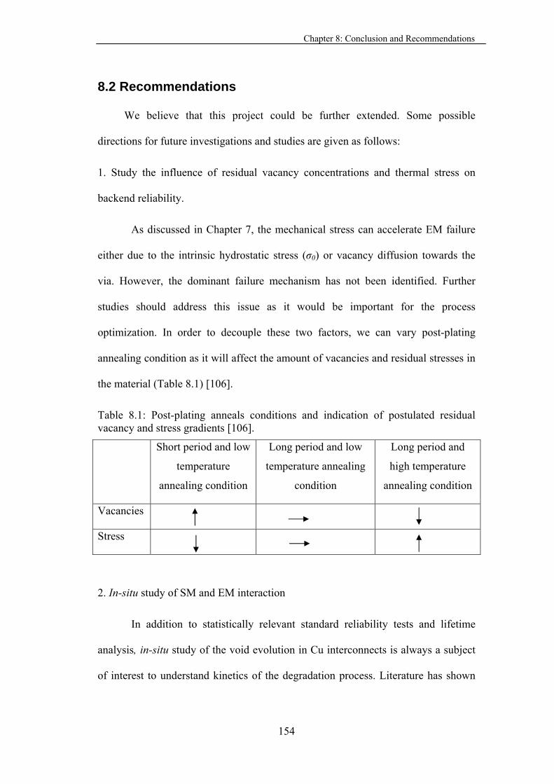
Chapter 8: Conclusion and Recommendations
154
8.2 Recommendations
We believe that this project could be further extended. Some possible
directions for future investigations and studies are given as follows:
1. Study the influence of residual vacancy concentrations and thermal stress on
backend reliability.
As discussed in Chapter 7, the mechanical stress can accelerate EM failure
either due to the intrinsic hydrostatic stress (σ0) or vacancy diffusion towards the
via. However, the dominant failure mechanism has not been identified. Further
studies should address this issue as it would be important for the process
optimization. In order to decouple these two factors, we can vary post-plating
annealing condition as it will affect the amount of vacancies and residual stresses in
the material (Table 8.1) [106].
Table 8.1: Post-plating anneals conditions and indication of postulated residual vacancy and stress gradients [106].
Short period and low
temperature
annealing condition
Long period and low
temperature annealing
condition
Long period and
high temperature
annealing condition
Vacancies
Stress
2. In-situ study of SM and EM interaction
In addition to statistically relevant standard reliability tests and lifetime
analysis, in-situ study of the void evolution in Cu interconnects is always a subject
of interest to understand kinetics of the degradation process. Literature has shown

Chapter 8: Conclusion and Recommendations
155
in-situ study of individual SM and EM, but the in-situ observation on the interaction
between these two failure mechanisms has not been reported. Our experimental
findings will be further established if other researchers can achieve the same results
with in-situ observation method.
3. Study the reliability of Cu-TSV
As discussed in Chapter 1, the interconnect signal RC delay becomes a critical
limiting factor in chip performance budgeting. When the dimensions of nanodevices
shrink, the total interconnect resistance increases rapidly due to the reduced line
cross-section and increased length of interconnects. For that reason, the
development of an alternate technology to design and fabricate a three-dimensional
(3D) circuit system is essential, to decrease in the overall wire length and reduce the
RC delay.
Through-silicon via (TSV) is considered to be the most promising technology
for 3D integration. It was forecast that 3D-TSV wafers could account for as much
as 6% of the total semiconductor industry and 25% of the memory market by 2015
[122]. While current efforts are focused on the development and improvement of
various TSV fabrication process steps, in-depth study of the associated new yield
and reliability issues in TSV is still limited. Ensuring adequate TSV reliability is
essential in order to commercialize 3D technology.
As SM and EM is an inherent wear-out mechanism in conductors, the void
formation process in TSV under SM and EM test should be investigated
experimentally to understand the physical mechanisms responsible for various

Chapter 8: Conclusion and Recommendations
156
failures modes of TSV. The dominant transport mechanisms, effect of electron flux,
metal migration routes, and activation energies needs detailed investigation. An
initial work has been carried out for SM study and the results are shown in
Appendix 1. We observed SM occurs in the TSV because large stress gradient
develop across the TSV and as a result, Cu atoms diffuse from the compressive to
tensile regions of the TSV to achieve stress relaxation and reach lowest system
energy configuration. Lastly, future research should also be carried out in order to
investigate the SM and EM interaction in the TSV.

Author’s Publications
157
AUTHOR’S PUBLICATIONS
1. A. Heryanto, K. L. Pey, Y. K. Lim, W. Liu, N. Raghavan, J. Wei, C. L. Gan, M.
K. Lim, and J. B. Tan, "The effect of stress migration on electromigration in
dual damascene copper interconnects," Journal of Applied Physics, vol. 109,
013716, 2011.
2. A. Heryanto, K. L. Pey, Y. K. Lim, N. Raghavan, W. Liu, J. Wei, C. L. Gan,
and J. B. Tan, "Stress migration risk on electromigration reliability in advanced
narrow line copper interconnects," Journal of Applied Physics, vol. 110, pp.
083702-5, 2011.
3. A. Heryanto, W.N. Putra, A. Trigg, S. Gao, F.X. Che, W.S. Kwon, X.F. Ang, J.
Wei, C.L. Gan, and K.L. Pey, “Microstructural Evolution of Copper TSV
During Annealing and its Effect on the Via Protrusion for TSV Wafer
Fabrication”, presented in International Conference on Materials for Advanced
Technology (ICMAT), MRS, Singapore, 2011.
4. A. Heryanto, K.L. Pey, Y.K. Lim, W. Liu, J. Wei, N. Raghavan, J.B. Tan, and
D.K. Sohn, “Study of Stress Migration and Electromigration Interaction in
Copper/Low-K Interconnects”, Proceedings of the 48th International Reliability
Physics Symposium (IRPS), IEEE, Anaheim, USA, 2010, p. 86-90.
5. A. Heryanto, Y.K. Lim, K.L. Pey, W. Liu, J.B. Tan, D.K. Sohn, and L.C. Hsia,
“The Effects of Dielectric Slots on Copper/Low-k Interconnects Reliability”,
Proceedings of the 12th International Interconnect Technology Conference
(IITC), IEEE, Sapporo, Japan, 2009, p. 92-94.
6. A. Heryanto, W. N. Putra, A. Trigg, S. Gao, W. S. Kwon, F. X. Che, X. F. Ang,
J. Wei, I. M. Riko, C. L. Gan, and K. L. Pey, “Effect of Copper TSV Annealing
on the Via Protrusion for TSV Wafer Fabrication”, accepted for publication in
Journal of Electronic Materials.
7. F. X. Che, W. N. Putra, A. Heryanto, A. Trigg, S. Gao and C. L. Gan,
“Numerical and Experimental Study on Cu Protrusion of Cu-Filled Through-
Silicon Vias (TSV)”, presented in International 3D System Integration
Conference, IEEE, Osaka, Japan, Feb 2012.

Bibliography
158
BIBLIOGRAPHY
[1] 2010 Update International Technology Roadmap for Semiconductors Report.
[2] G. E. Moore, Electronics, vol. 38(8), pp. 114-17. [3] M. Kanellos. (2005). New Life for Moore's Law. Available:
http://news.cnet.com/New-life-for-Moores-Law/2009-1006_3-5672485.html [4] Available:
http://upload.wikimedia.org/wikipedia/commons/0/00/Transistor_Count_and_Moore%27s_Law_-_2011.svg
[5] M. T. Bohr, "Interconnect scaling-the real limiter to high performance ULSI," New York, NY, USA, 1995, pp. 241-4.
[6] D. Edelstein, J. Heidenreich, R. Goldblatt, W. Cote, C. Uzoh, N. Lustig, P. Roper, T. McDevitt, W. Motsiff, A. Simon, J. Dukovic, R. Wachnik, H. Rathore, R. Schulz, L. Su, S. Luce, and J. Slattery, "Full copper wiring in a sub-0.25 m CMOS ULSI technology," New York, NY, USA, 1997, pp. 773-6.
[7] W. H. Dresher. (2000). Speeding-up Your Computer in the 21st Century Using Copper ICs. Available: http://www.copper.org/publications/ newsletters/innovations/2000/01/speeding_up.html
[8] R. S. List, A. Singh, A. Ralston, and G. Dixit. (1997) Integration of low-k dielectric materials into sub-0.25-μm interconnects. MRS Bulletin. 61.
[9] C. D. Hartfield, E. T. Ogawa, P. Young-Joon, C. Tz-Cheng, and G. Honglin, "Interface reliability assessments for copper/low-k products," IEEE Transactions on Device and Materials Reliability, vol. 4, pp. 129-41, 2004.
[10] H. J. Yoo, S. Balakrishnan, J. Bielefeld, M. Harmes, H. Hiramatsu, S. King, M. Kobrinsky, B. Krist, P. Reese, V. RamachandraRao, K. Singh, S. Suri, and C. Ward, "Demonstration of a Reliable High-Performance and Yielding Air gap Interconnect Process," in 2010 IEEE International Interconnect Technology Conference - IITC, 6-9 June 2010, Piscataway, NJ, USA, 2010, p. 3 pp.
[11] R. C. Johnson. (2007). IBM pitches air gaps as 'ultimate' dielectric. Available: http://www.eetasia.com/ART_8800468719_NT_38e0f8f1.HTM
[12] Available: http://www-03.ibm.com/press/us/en/presskit/21463.wss. [13] K. N. Tu, "Recent advances on electromigration in very-large-scale-
integration of interconnects," Journal of Applied Physics, vol. 94, pp. 5451-73, 2003.
[14] C. J. Zhai, H. W. Yao, A. P. Marathe, P. R. Besser, and R. C. Blish Ii, "Simulation and experiments of stress migration for Cu/low-k BEoL," IEEE Transactions on Device and Materials Reliability, vol. 4, pp. 523-528, 2004.
[15] J. M. Paik, H. Park, and Y. C. Joo, "Effect of low-k dielectric on stress and stress-induced damage in Cu interconnects," Microelectronic Engineering, vol. 71, pp. 348-357, 2004.
[16] J. R. Lloyd, "Electromigration failure," Journal of Applied Physics, vol. 69, pp. 7601-7604, 1991.

Bibliography
159
[17] J. Curry, G. Fitzgibbon, Y. Guan, R. Muollo, G. Nelson, and A. Thomas, "New Failure Mechanisms in Sputtered Aluminum-Silicon Films," in Reliability Physics Symposium, 1984. 22nd Annual, 1984, pp. 6-8.
[18] J. T. Yue, W. P. Funsten, and R. V. Taylor, "Stress Induced Voids in Aluminum Interconnects During IC Processing," in Reliability Physics Symposium, 1985. 23rd Annual, 1985, pp. 126-137.
[19] T. Turner and K. Wendel, "The Influence of Stress on Aluminum Conductor Life," in Reliability Physics Symposium, 1985. 23rd Annual, 1985, pp. 142-147.
[20] A. W. Strong, E. Y. Wu, R.-P. Vollertsen, J. Sune, G. L. Rosa, T. D. Sullivan, and S. E. Rauch, Reliability Wearout Mechanisms in Advanced CMOS Technologies: Wiley-IEEE Press, 2009.
[21] C. J. Zhai, H. W. Yao, P. R. Besser, A. Marathe, R. C. Blish, II, D. Erb, C. Hau-Riege, S. Taylor, and K. O. Taylor, "Stress modeling of Cu/low-k BEoL - application to stress migration," in Reliability Physics Symposium Proceedings, 2004. 42nd Annual. 2004 IEEE International, 2004, pp. 234-239.
[22] J. W. McPherson and C. F. Dunn, "A model for stress-induced metal notching and voiding in very large-scale-integrated Al-Si (1%) metallization," Journal of Vacuum Science & Technology B (Microelectronics Processing and Phenomena), vol. 5, pp. 1321-5, 1987.
[23] E. T. Ogawa, J. W. McPherson, J. A. Rosal, K. J. Dickerson, T. C. Chiu, L. Y. Tsung, M. K. Jain, T. D. Bonifield, J. C. Ondrusek, and W. R. McKee, "Stress-induced voiding under vias connected to wide Cu metal leads," Piscataway, NJ, USA, 2002, pp. 312-21.
[24] S. H. Rhee, D. Yong, and P. S. Ho, "Thermal stress characteristics of Cu/oxide and Cu/low-k submicron interconnect structures," Journal of Applied Physics, vol. 93, pp. 3926-33, 2003.
[25] J. Gambino, T. C. Lee, F. Chen, and T. D. Sullivan, "Reliability of Copper Interconnects: Stress-Induced Voids," ECS Transactions, vol. 18, pp. 205-211, 2009.
[26] Y. K. Lim, K. L. Pey, P. S. Lee, Y. H. Lee, N. R. Kamat, J. B. Tan, T. Fu, and L. C. Hsia, "Design for manufacturability and its role in enhancing stress migration reliability of porous ultra low-k copper interconnects," in 2007 IEEE International Reliability Physics Symposium Proceedings, 15-19 April 2007, Piscataway, NJ, USA, 2007, p. 7 pp.
[27] Y. K. Lim, Ph.D Thesis, School of Electrical and Electronic Engineering, Nanyang Technological University, 2008.
[28] T. Suzuki, A. Uedono, T. Nakamura, Y. Mizushima, H. Kitada, and Y. Koura, "Direct observation of vacancy defects in electroplated Cu films," in Interconnect Technology Conference, 2004. Proceedings of the IEEE 2004 International, 2004, pp. 87-89.
[29] G. B. Alers, "Via Voids and Via Stress Migration," presented at the IEEE 42nd Annual International Reliability Physics Symposium Tutorial, 2004.
[30] G. B. Alers, D. Dornisch, J. Siri, K. Kattige, L. Tam, E. Broadbent, and G. W. Ray, "Trade-off between reliability and post-CMP defects during recrystallization anneal for copper damascene interconnects," in Reliability

Bibliography
160
Physics Symposium, 2001. Proceedings. 39th Annual. 2001 IEEE International, 2001, pp. 350-354.
[31] H. Okabayashi, "Stress-induced void formation in metallization for integrated circuits," Materials Science & Engineering R: Reports, vol. R11, pp. 191-241, 1993.
[32] K. Yoshida, T. Fujimaki, K. Miyamoto, T. Honma, H. Kaneko, H. Nakazawa, and M. Morita, "Stress-induced voiding phenomena for an actual CMOS LSI interconnects," in IEEE International Electron Devices Meeting, 8-11 Dec. 2002, Piscataway, NJ, USA, 2002, pp. 753-6.
[33] T. Oshima, K. Hinode, H. Yamaguchi, H. Aoki, K. Torii, T. Saito, K. Ishikawa, J. Noguchi, M. Fukui, T. Nakamura, S. Uno, K. Tsugane, J. Murata, K. Kikushima, H. Sekisaka, E. Murakami, K. Okuyama, and T. Iwasaki, "Suppression of stress-induced voiding in copper interconnects," in IEEE International Electron Devices Meeting, 8-11 Dec. 2002, Piscataway, NJ, USA, 2002, pp. 757-60.
[34] M. Kawano, T. Fukase, Y. Yamamoto, T. Ito, S. Yokogawa, H. Tsuda, Y. Kunimune, T. Saitoh, K. Ueno, and M. Sekine, "Stress relaxation in dual-damascene Cu interconnects to suppress stress-induced voiding," in Interconnect Technology Conference, 2003. Proceedings of the IEEE 2003 International, 2003, pp. 210-212.
[35] A. V. Glasow, A. H. Fischer, M. Hierlemann, S. Penka, and F. Ungar, "Geometrical aspects of stress-induced voiding in copper interconnects," in Advanced Metallization Conference, 2002.
[36] E. Zschech, R. Huebner, D. Chumakov, O. Aubel, D. Friedrich, P. Guttmann, S. Heim, and G. Schneider, "Stress-induced phenomena in nanosized copper interconnect structures studied by x-ray and electron microscopy," Journal of Applied Physics, vol. 106, pp. 093711-5, 2009.
[37] M. Gerardin, Compt. Rend. Acad. Sci. Paris, vol. 53, p. 727, 1861. [38] I.A. Blech and H. Sello, "A study of failure mechanisms in silicon planar
epitaxial transistors," T.S. Shilliday, J. Vaccaro (Eds.), Physics of Failure in Electronics, vol. 5, pp. 265-280, 1966.
[39] C. S. Hau-Riege, "An introduction to Cu electromigration," Microelectronics Reliability, vol. 44, pp. 195-205, 2004.
[40] S. J. Yoon, Ph.D Thesis, The University of Texas at Austin, 2005. [41] I. A. Blech and C. Herring, "Stress generation by electromigration," Applied
Physics Letters, vol. 29, pp. 131-3, 1976. [42] M. Gall, M. Hauschildt, and R. Hernandez, "Large-scale statistical analysis
of early failures in Cu electromigration, Part II: Scaling behavior and short-length effects," Journal of Applied Physics, vol. 108, pp. 013524-6, 2010.
[43] K. D. Lee, E. T. Ogawa, H. Matsuhashi, P. R. Justison, K. Kil-Soo, P. S. Ho, and V. A. Blaschke, "Electromigration critical length effect in Cu/oxide dual-damascene interconnects," Applied Physics Letters, vol. 79, pp. 3236-8, 2001.
[44] C. S. Hau-Riege, S. P. Hau-Riege, and A. P. Marathe, "The effect of interlevel dielectric on the critical tensile stress to void nucleation for the reliability of Cu interconnects," Journal of Applied Physics, vol. 96, pp. 5792-6, 2004.

Bibliography
161
[45] M. A. Korhonen, P. Borgesen, K. N. Tu, and L. Che-Yu, "Stress evolution due to electromigration in confined metal lines," Journal of Applied Physics, vol. 73, pp. 3790-9, 1993.
[46] J. J. Clement and C. V. Thompson, "Modeling electromigration-induced stress evolution in confined metal lines," Journal of Applied Physics, vol. 78, pp. 900-904, 1995.
[47] F. Wei, Ph.D Thesis, Materials Science and Engineering, Massachusetts Institute of Technology, 2007.
[48] T. G. Koetter, H. Wendrock, H. Schuehrer, C. Wenzel, and K. Wetzig, "Relationship between microstructure and electromigration damage in unpassivated PVD copper damascene interconnects," in ESREF 2000. 11th European Symposium on the Reliability of Electron Devices, 2-6 Oct. 2000, UK, 2000, pp. 1295-9.
[49] K. L. Lee, C. K. Hu, and K. N. Tu, "In situ scanning electron microscope comparison studies on electromigration of Cu and Cu(Sn) alloys for advanced chip interconnects," Journal of Applied Physics, vol. 78, pp. 4428-4437, 1995.
[50] J. Proost, T. Hirato, T. Furuhara, K. Maex, and J. P. Celis, "Microtexture and electromigration-induced drift in electroplated damascene Cu," Journal of Applied Physics, vol. 87, pp. 2792-2802, 2000.
[51] A. V. Vairagar, S. G. Mhaisalkar, A. Krishnamoorthy, K. N. Tu, A. M. Gusak, M. A. Meyer, and E. Zschech, "In situ observation of electromigration-induced void migration in dual-damascene Cu interconnect structures," Applied Physics Letters, vol. 85, pp. 2502-2504, 2004.
[52] E. Liniger, L. Gignac, C. K. Hu, and S. Kaldor, "In situ study of void growth kinetics in electroplated Cu lines," Journal of Applied Physics, vol. 92, pp. 1803-1810, 2002.
[53] C. K. Hu, R. Rosenberg, and K. Y. Lee, "Electromigration path in Cu thin-film lines," Applied Physics Letters, vol. 74, pp. 2945-7, 1999.
[54] Y. M. M. T. Surholt, and C. Herzig, Phys. Rev. B, vol. 50, p. 3577, 1994. [55] T. Surholt and C. Herzig, Acta Mater, vol. 45, p. 3817, 1997. [56] D. Gupta, C.-K. Hu, and K. L. Lee, Defect Diffusion Forum, vol. 143, 1997. [57] C. K. Hu, L. Gignac, E. Liniger, R. Rosenberg, and A. Stamper, in Proc.
IEEE 2002 Int. Interconnect Technol. Conf., 2002, p. 133. [58] S. Tokogawa and H. Takizawa, in Proc. IEEE Int. Interconnect Tech. Conf,
2002, p. 127. [59] D. B. Butrymowicz, J. R. Manning, and M. E. Reed, J. Phys. Chem.
Reference Data, vol. 2, p. 643, 1977. [60] M. D. Arnaud L. Trtavel G. Berger T, Gobil Y, Touet I., Microelectronics
Reliability, vol. 40, p. 77, 2000. [61] C. K. Hu, L. Gignac, R. Rosenberg, E. Liniger, J. Rubino, C. Sambucetti, A.
Stamper, A. Domeni-cucci, and X. Chen, Microelectronic Eng., vol. 70, p. 406, 2003.
[62] C. K. Hu, L. Gignac, E. Liniger, B. Herbst, D. Rath, S. T. Chen, S. Kaldor, A. Simon, and W. T. Tseng, Appl. Phys. Lett., vol. 83, p. 869, 2003.
[63] C. L. Gan, C. V. Thompson, K. L. Pey, W. K. Choi, H. L. Tay, B. Yu, and M. K. Radhakrishnan, "Effect of current direction on the lifetime of different

Bibliography
162
levels of Cu dual-damascene metallization," Applied Physics Letters, vol. 79, pp. 4592-4594, 2001.
[64] M. H. Lin, Y. L. Lin, J. M. Chen, M. S. Yeh, K. P. Chang, K. C. Su, and W. Tahui, "Electromigration lifetime improvement of copper interconnect by cap/dielectric interface treatment and geometrical design," Electron Devices, IEEE Transactions on, vol. 52, pp. 2602-2608, 2005.
[65] E. G. Liniger, C. K. Hu, L. M. Gignac, and A. Simon, "Effect of liner thickness on electromigration lifetime," Journal of Applied Physics, vol. 93, pp. 9576-9582, 2003.
[66] A. S. Oates and M. H. Lin, "Electromigration Failure Distributions of Cu/Low-k Dual-Damascene Vias: Impact of the Critical Current Density and a New Reliability Extrapolation Methodology," Device and Materials Reliability, IEEE Transactions on, vol. 9, pp. 244-254, 2009.
[67] K. D. Lee, P. Young-Joon, K. Tae, and W. R. Hunter, "Via Processing Effects on Electromigration in 65 nm Technology," in Reliability Physics Symposium Proceedings, 2006. 44th Annual., IEEE International, 2006, pp. 103-106.
[68] A. H. Fischer, A. von Glasow, S. Penka, and F. Ungar, "Process optimization-the key to obtain highly reliable Cu interconnects," in Interconnect Technology Conference, 2003. Proceedings of the IEEE 2003 International, 2003, pp. 253-255.
[69] S. C. Lee and A. S. Oates, "Identification and Analysis of Dominant Electromigration Failure Modes in Copper/Low-K Dual Damascene Interconnects," in Reliability Physics Symposium Proceedings, 2006. 44th Annual., IEEE International, 2006, pp. 107-114.
[70] A. S. Oates, "Electromigration in stress-voided Al alloy conductors," in Reliability Physics Symposium, 1993. 31st Annual Proceedings., International, 1993, pp. 297-303.
[71] N. Matsunaga, H. Shibata, and K. Hashimoto, "Influence of stress-induced void formation on electromigration endurance in quarter-micron aluminum interconnects," in VLSI Technology, 1992. Digest of Technical Papers. 1992 Symposium on, 1992, pp. 76-77.
[72] C. A. Minor, Y. L. Guo, and Y. L. Shen, "On the propensity of electromigration void growth from preexisting stress-voids in metal interconnects," Scripta Materialia, vol. 41, pp. 347-52, 1999.
[73] A. H. Fischer and A. E. Zitzelsberger, "The quantitative assessment of stress-induced voiding in process qualification," in Reliability Physics Symposium, 2001. Proceedings. 39th Annual. 2001 IEEE International, 2001, pp. 334-340.
[74] "Constant Temperature Aging to Characterize Aluminum Interconnect Metallization for Stress-Induced Voiding." vol. JEP 139, ed: JEDEC Publication, Dec 2000.
[75] J. R. Black, "Electromigration Failure Modes in Aluminum Metallization for Semiconductor Devices," 57, 1969.
[76] P. K. Tan, Z. H. Mai, Y. W. Goh, L. Zhu, S. L. Toh, Q. Deng, R. He, H. Tan, H. L. Li, Q. F. Wang, Y. Z. Ma, W. Y. Lee, G. R. Low, and J. Lam, "Fault Isolation on High Resistance Failure of 45nm ET Via Chains Using Combined Technique of SEM PVC and Nanoprobing," in 36th International

Bibliography
163
Symposium for Testing and Failure Analysis (ISTFA 2010), 14-18 Nov. 2010, Materials Park, OH, USA, 2010, pp. 239-42.
[77] C. M. Tan and N. Raghavan, "Unveiling the electromigration physics of ULSI interconnects through statistics," Semiconductor Science and Technology, vol. 22, pp. 941-6, 2007.
[78] H. Akaike, "A new look at the statistical model identification," IEEE Transactions on Automatic Control, vol. AC-19, pp. 716-23, 1974.
[79] A. P. Dempster, N. M. Laird, and D. B. Rubin, "Maximum likelihood from incomplete data via the EM algorithm," J. R. Stat. Soc., vol. 39, pp. 1-38, 1977.
[80] S. Jiang and D. Kececioglu, "Maximum likelihood estimates, from censored data, for mixed-Weibull distributions," IEEE Transactions on Reliability, vol. 41, pp. 248-255, 1992.
[81] G. Zhang, C. M. Tan, K. T. Tan, K. Y. Sim, and W. Y. Zhang, "Reliability improvement in Al metallization: a combination of statistical prediction and failure analytical methodology," in 15th European Symposium on the Reliability of Electron Devices, Failure Physics and Analysis (ESREF 2004), 4-8 Oct. 2004, UK, 2004, pp. 1843-8.
[82] B. Li, C. Christiansen, J. Gill, T. Sullivan, E. Yashchin, and R. Filippi, "Threshold electromigration failure time and its statistics for Cu interconnects," Journal of Applied Physics, vol. 100, pp. 114516-1, 2006.
[83] M. Murakami, T. S. Kuan, and I. A. Blech, "“Mechanical Properties of Thin Films on Substrates," Treatise on Materials Science and Technology, vol. 24, pp. 163-209, 1982.
[84] W. D. Nix, Metall. Trans. A, vol. 20A, 1989. [85] M. F. Doerner and W. D. Nix, CRC Crit. Rev. Solid State Mater. Sci., vol.
14, p. 225, 1988. [86] C. P. Wang, S. Lopatin, A. Marathe, M. Buynoski, R. Huang, and D. Erb,
"Binary Cu-alloy layers for Cu-interconnections reliability improvement," in Proceedings of the IEEE 2001 International Interconnect Technology Conference, 4-6 June 2001, Piscataway, NJ, USA, 2001, pp. 86-8.
[87] C. K. Hu, K. Y. Lee, K. L. Lee, C. Cabral, Jr., E. G. Colgan, and C. Stanis, "Electromigration drift velocity in Al-alloy and Cu-alloy lines," in Proceedings of Reliability of Metals in Electronics, 21-26 May 1995, Pennington, NJ, USA, 1995, pp. 203-14.
[88] C. K. Hu, L. Gignac, R. Rosenberg, E. Liniger, J. Rubino, C. Sambucetti, A. Domenicucci, X. Chen, and A. K. Stamper, "Reduced electromigration of Cu wires by surface coating," Applied Physics Letters, vol. 81, pp. 1782-4, 2002.
[89] Y. K. Lim, Y. H. Lim, C. S. Seet, B. C. Zhang, K. L. Chok, K. H. See, T. J. Lee, L. C. Hsia, and K. L. Pey, "Stress-induced voiding in multi-level copper/low-k interconnects," in 2004 IEEE International Reliability Physics Symposium. Proceedings, 25-29 April 2004, Piscataway, NJ, USA, 2004, pp. 240-5.
[90] M. Lin, N. Jou, J. W. Liang, and K. C. Su, "Effect of multiple via layout on electromigration performance and current density distribution in copper interconnect," in 2009 IEEE International Reliability Physics Symposium (IRPS), 26-30 April 2009, Piscataway, NJ, USA, 2009, pp. 844-7.

Bibliography
164
[91] M. Lin, N. Jou, J. W. Liang, A. Juan, and K. C. Su, "Effect of multiple via structure on upstream electromigration in copper interconnect," in 2009 16th IEEE International Symposium on the Physical and Failure Analysis of Integrated Circuits (IPFA), 6-10 July 2009, Piscataway, NJ, USA, 2009, pp. 603-7.
[92] Y. K. Lim, Y. H. Lim, N. R. Kamat, A. See, T. J. Lee, and K. L. Pey, "Stress-induced voiding beneath vias with wide copper metal leads," in Proceedings of the 11th International Symposium on the Physical and Failure Analysis of Integrated Circuits. IPFA 2004, 5-8 July 2004, Piscataway, NJ, USA, 2004, pp. 103-6.
[93] T. C. Huang, C. H. Yao, W. K. Wan, C. C. Hsia, and M. S. Liang, "Numerical modeling and characterization of the stress migration behaviour upon various 90 nanometer Cu/Low k interconnects," in IEEE International Interconnect Technology Conference, 2-4 June 2003, Piscataway, NJ, USA, 2003, pp. 207-9.
[94] B. Li, J. Gill, C. J. Christiansen, T. D. Sullivan, and P. S. McLaughlin, "Impact of via-line contact on Cu interconnect electromigration performance," in 2005 IEEE International Reliability Physics Symposium. Proceedings 43rd Annual, 17-21 April 2005, Piscataway, NJ, USA, 2005, pp. 24-30.
[95] Y. K. Lim, K. L. Pey, J. B. Tan, T. J. Lee, D. Vigar, L. C. Hsia, Y. H. Lim, and N. R. Kamat, "Novel dielectric slots in Cu interconnects for suppressing stress-induced void failure," Piscataway, NJ, USA, 2005, p. 4 pp.
[96] G. D. R. Hall, D. D. J. Allman, and H. D. Bhatt, "Impact of via interactions and metal slotting on stress induced voiding," Piscataway, NJ, USA, 2008, pp. 392-8.
[97] K. N. Tu, J. W. Mayer, and L. C. Feldman, Electronic thin film science: for electrical engineers and materials scientists, 1992.
[98] J. R. Lloyd, "Electromigration in integrated circuit conductors," Journal of Physics D (Applied Physics), vol. 32, pp. 109-18, 1999.
[99] B. Baerg, "Recent problems in electromigration testing," in 1997 IEEE International Reliability Physics Symposium Proceedings. 35th Annual, 8-10 April 1997, New York, NY, USA, 1997, pp. 211-15.
[100] E. T. Ogawa, K. D. Lee, H. Matsuhashi, K. S. Ko, P. R. Justison, A. N. Ramamurthi, A. J. Bierwag, P. S. Ho, V. A. Blaschke, and R. H. Havemann, "Statistics of electromigration early failures in Cu/oxide dual-damascene interconnects," in 2001 IEEE International Reliability Physics Symposium Proceedings. 39th Annual, 30 April-3 May 2001, Piscataway, NJ, USA, 2001, pp. 341-9.
[101] C. J. Christiansen, L. Baozhen, J. Gill, R. Filippi, and M. Angyal, "Via-depletion electromigration in copper interconnects," IEEE Transactions on Device and Materials Reliability, vol. 6, pp. 163-8, 2006.
[102] A. Grill, V. Patel, K. P. Rodbell, E. Huang, M. R. Baklanov, K. P. Mogilnikov, M. Toney, and H. C. Kim, "Porosity in plasma enhanced chemical vapor deposited SiCOH dielectrics: a comparative study," Journal of Applied Physics, vol. 94, pp. 3427-35, 2003.
[103] M. H. Lin, Y. L. Lin, K. P. Chang, K. C. Su, and T. Wang, "Copper interconnect electromigration behavior in various structures and precise

Bibliography
165
bimodal fitting," Japanese Journal of Applied Physics, Part 1 (Regular Papers, Short Notes & Review Papers), vol. 45, pp. 700-9, 2006.
[104] E. Zschech, R. Hubner, O. Aubel, and P. S. Ho, "EM and SM induced degradation dynamics in copper interconnects studied using electron microscopy and X-ray microscopy," in 2010 IEEE International Reliability Physics Symposium (IRPS 2010), 2-6 May 2010, Piscataway, NJ, USA, 2010, pp. 574-80.
[105] M. Hauschildt, M. Gall, and R. Hernandez, "Large-scale statistical analysis of early failures in Cu electromigration. Part I: dominating mechanisms," Journal of Applied Physics, vol. 108, p. 013523 (10 pp.), 2010.
[106] K. Croes, C. J. Wilson, M. Lofrano, B. Vereecke, G. P. Beyer, and Z. Tokei, "Electromigration and stress-induced-voiding in dual damascene Cu/low-k interconnects: a complex balance between vacancy and stress gradients," in 2010 IEEE International Reliability Physics Symposium (IRPS 2010), 2-6 May 2010, Piscataway, NJ, USA, 2010, pp. 591-8.
[107] A. Grill, "Plasma enhanced chemical vapor deposited SiCOH dielectrics: from low-k to extreme low-k interconnect materials," Journal of Applied Physics, vol. 93, pp. 1785-1790, 2003.
[108] Y. K. Lim, R. Arijit, K. L. Pey, C. M. Tan, C. S. Seet, T. J. Lee, and D. Vigar, "Stress migration reliability of wide Cu interconnects with gouging vias," Piscataway, NJ, USA, 2005, pp. 203-8.
[109] R. A. Wachnik, R. G. Filippi, T. M. Shaw, and P. C. Lin, "Practical benefits of the electromigration short-length effect, including a new design rule methodology and an electromigration resistant power grid with enhanced wireability," in 2000 Symposium on VLSI Technology. Digest of Technical Papers, 13-15 June 2000, Piscataway, NJ, USA, 2000, pp. 220-1.
[110] M. H. Lin, M. T. Lin, and W. Tahui, "Effects of length scaling on electromigration in dual-damascene copper interconnects," Microelectronics Reliability, vol. 48, pp. 569-77, 2008.
[111] K. Y. Y. Doong, R. C. J. Wang, S. C. Lin, L. J. Hung, C. C. Chiu, D. Su, K. Wu, K. L. Young, and Y. K. Peng, "Stress-induced voiding and its geometry dependency characterization," Piscataway, NJ, USA, 2003, pp. 156-60.
[112] S. J. Lee, S. G. Lee, B. S. Suh, H. Shin, N. I. Lee, H. K. Kang, and G. Suh, "New insight into stress induced voiding mechanism in Cu interconnects," Piscataway, NJ, USA, 2005, pp. 108-10.
[113] T. Suzuki, T. Nakamura, Y. Mizushima, T. Kouno, M. Shiozu, S. Otsuka, T. Hosoda, H. Matsuyama, and K. Shono, "Stress migration phenomenon in narrow copper interconnects," Journal of Applied Physics, vol. 101, pp. 044513-5, 2007.
[114] R. G. Filippi, P. C. Wang, A. Brendler, P. S. McLaughlin, J. Poulin, B. Redder, J. R. Lloyd, and J. J. Demarest, "The effect of a threshold failure time and bimodal behavior on the electromigration lifetime of copper interconnects," Piscataway, NJ, USA, 2009, pp. 444-51.
[115] A. S. Budiman, C. S. Hau-Riege, W. C. Baek, C. Lor, A. Huang, H. S. Kim, G. Neubauer, J. Pak, P. R. Besser, and W. D. Nix, "Electromigration-induced plastic deformation in Cu interconnects: Effects on current density exponent, n, and implications for em reliability assessment," Journal of Electronic Materials, vol. 39, pp. 2483-2488, 2010.

Bibliography
166
[116] C. J. Wilson, K. Croes, C. Zhao, T. H. Metzger, L. Zhao, G. P. Beyer, A. B. Horsfall, A. G. O'Neill, x, and Z. kei, "Synchrotron measurement of the effect of linewidth scaling on stress in advanced Cu/Low-k interconnects," Journal of Applied Physics, vol. 106, pp. 053524-7, 2009.
[117] J. R. Lloyd, "Black's law revisited - nucleation and growth in electromigration failure," Microelectronics Reliability, vol. 47, pp. 1468-72, 2007.
[118] Available: http://en.wikipedia.org/wiki/Log-normal_distribution [119] V. M. Dwyer, "An investigation of electromigration induced void nucleation
time statistics in short copper interconnects," Journal of Applied Physics, vol. 107, pp. 103718-12, 2010.
[120] C. J. Wilson, K. Croes, Z. Tokei, B. Vereecke, G. P. Beyer, A. G. O'Neill, and A. B. Horsfall, "Application of a nano-mechanical sensor to monitor stress in copper damascene interconnects," Applied Physics Express, vol. 2, 2009.
[121] C. E. Murray, P. R. Besser, C. Witt, and J. L. Jordan-Sweet, "Stress gradients induced in Cu films by capping layers," Applied Physics Letters, vol. 93, pp. 221901-3, 2008.
[122] Industry Leaders Outline 3D TSV Revolution Available: http://www.semi.org/en/P044605

Appendix A: Microstructural Evolution of Copper TSV During Annealing and its Effect on the Via Protrusion for TSV Wafer Fabrication
167
APPENDIX A
MICROSTRUCTURAL EVOLUTION OF COPPER TSV
DURING ANNEALING AND ITS EFFECT ON THE VIA
PROTRUSION FOR TSV WAFER FABRICATION
A.1. Introduction
Chip interconnect resistance has always been one of the key challenges
identified by the International Technology Roadmap for Semiconductors (ITRS)
[1]. When the dimensions of nanodevices shrink, the total interconnect resistance
increases rapidly due to the reduced line cross-section and increased length of
interconnects. Consequently, the interconnect signal RC delay continues to increase
and becomes a critical limiting factor in chip performance budgeting. Therefore, the
development of an alternate technology to design and fabricate a three-dimensional
(3D) circuit system becomes essential, as adherence to Moore’s law gets
increasingly difficult with conventional planar downscaling, solely by transistor
design and fabrication innovations. 3D integrated-circuit (IC) is a developing
technology that vertically stacks multiple dies with a high density die-to-die
interconnect. This results in a decrease in the overall wire length, providing a
reduction in wire delay.
3D stack packages were initially developed for memory packages for
cellular phones with wire bonding used as an interconnection between the stacked
devices and the circuit board [2]. However, wire bonding is not appropriate for high
performance and has several disadvantages such as limitation of the size reduction

Appendix A: Microstructural Evolution of Copper TSV During Annealing and its Effect on the Via Protrusion for TSV Wafer Fabrication
168
and drop in high frequency characteristics [3,4]. A 3D technology with through-
silicon vias (TSVs) aligned on a tight pitch was one of the new technologies to meet
that challenge [5,6]. TSV technology can offer excellent electrical performance and
possibility of advanced wafer-level 3D packaging or stacking of various types of
microcomponents directly on a chip [7-9].
While current efforts are focused on the development and improvement of
various TSV fabrication process steps, efforts to study in-depth the associated new
yield and reliability issues in TSV are still limited [10]. Ensuring adequate TSV
reliability is essential in order to commercialize 3D technology. Thermo-mechanical
reliability is one of the top reliability concerns, because process conditions during
subsequent back-end-of-line (BEOL) and die-stacking processes subject the Si
wafers containing TSVs to repeated thermal loadings. Due to the mismatch in
thermal expansion coefficients (CTEs) between the TSV material, surrounding
dielectric and the Si substrate, thermal stresses can develop in the silicon and
interconnect structures, causing several reliability concerns such as cracking,
delamination and voiding.
It has been reported that the performance of the transistor device is degraded
due to its sensitivity to stresses induced by the integration of TSV in the chip. A
stress of 100 MPa can change by over 7% the carrier mobility in MOSFET devices
[11]. In addition, the interface between the TSV and the Si substrate can be
delaminated due to the shear stress concentration at the edge of the TSV [12].
Another reliability concern is the TSV extrusion or TSV pumping problem. During
TSV manufacturing processes, Cu TSVs were found to extrude of the Si wafer
surface, causing fracture of the overlaying dielectric material. This is a potential

Appendix A: Microstructural Evolution of Copper TSV During Annealing and its Effect on the Via Protrusion for TSV Wafer Fabrication
169
threat to the IC interconnection layer, particularly for low-κ materials, since it can
lead to cracking of the dielectric layer in the BEOL structure.
Protrusion studies of the TSV have recently been reported in the literature
[12-14]. It was observed that if the TSV does not receive a proper thermal treatment
prior to BEOL processing (with some steps reaching 400°C), it will bulge upwards
and deform the metal/dielectric stack on top [13]. Further studies have reported that
the initial heat treatment at 420ºC for 20 minutes could solve this problem of TSV
protrusion [14]. The hypothesis is that during the first thermal cycling, the Cu-film
undergoes material transformation, such as grain growth and recrystallization, thus
resulting in an open hysteresis loop. The succeeding cycles after the first cycle are
found to have closed hysteresis loops that are similar in shape, size and position.
This means that the material behavior of Cu-film becomes stable after the first cycle
to the maximum thermal cycling condition.
Since TSV protrusion has a huge potential impact on the reliability of the
final 3D stack, further in-depth physical analysis investigations are needed. It is
important to correlate the Cu protrusion to the microstructural changes during
thermal annealing, so that the fabrication process can be further optimized. In this
paper, TSV protrusions at various annealing conditions have been characterized.
The grain size distribution is evaluated using the electron backscatter diffraction
(EBSD) method, following which, the material properties are evaluated using the
nano-indentation technique. Finally, possible solutions for further process
optimization are discussed.

Appendix A: Microstructural Evolution of Copper TSV During Annealing and its Effect on the Via Protrusion for TSV Wafer Fabrication
170
A.2. Test Structure Design and Process Methodology
Figure A.1 shows the schematic diagram of the test structure used in this
study, which consists of a 10 x 10 array of TSVs. The diameter of TSV is 5 μm,
with a pitch ratio of 1:2. The 50 μm depths of vias (aspect ratio 1:10) were formed
by a deep-reactive-ion-etching (DRIE) process on 300 mm silicon wafers. To avoid
shorting to the silicon, the etched vias were deposited with an insulating layer of
oxide (dielectric) before being filled with metal. The chemical vapor deposition
(CVD) technique with high inherent conformality was used for the dielectric lining.
After that, a thin layer of Ta-based diffusion barrier was deposited on the via
sidewalls for Cu TSVs using a physical vapor deposition (PVD) process. This is
followed by a conformal Cu seed layer deposited on via sidewalls/via bottom,
followed by electrodeposition of the via with copper. Lastly, any overplated Cu
from the via on the wafer top surface was removed by the chemical-mechanical
polishing (CMP) process.
Fig. A.1: Schematic diagram of the (a) top view of an array of TSVs (10x10) and (b) TSV cross section used in this study. The via diameter is 5 μm, with a pitch ratio of 1:2 and a depth of 50 μm.

Appendix A: Microstructural Evolution of Copper TSV During Annealing and its Effect on the Via Protrusion for TSV Wafer Fabrication
171
In this sample, there was no overlaying material on top of the TSVs. As a
result, the Cu-TSVs are free to expand in the out-of-plane direction and the Cu-
extrusion can be characterized. The influence of the annealing process on TSV-
protrusion was studied, in which the samples were subjected to a range of annealing
conditions, from TANN ~ 250-450°C with 50°C step. In these experiments, the
temperature ramp rate was set to 100°C/min and annealing temperature was
maintained for 30 minutes. The furnace temperature stability is ±1°C. The
annealing processes were performed under nitrogen gas ambient.
A.3. Results and Discussion
A. Protrusion Characterization
The Cu-TSV protrusion was characterized using scanning electron
microscopy (SEM), 3D surface profilometer and atomic force microscopy (AFM),
to observe the morphology and size of Cu protrusion. Figure A.2 shows SEM
micrographs of one of the protruding TSVs for various annealing conditions. It
shows that the shape of the protrusion depends on the annealing temperature. The
Cu protrusion can be visually observed starting from TANN = 350°C and it may occur
at either the center or the outer edge of the TSV (Figs. 2(c) and (d)). It may bulge
upwards as well, as shown in Fig. A.2(e).
In order to observe a variation of the TSV protrusion morphology across the
die, a 3D surface profilometer was employed. It is a noncontact optical profiler
system that uses two technologies to measure a wide range of surface heights:
phase-shifting interferometry (PSI) mode, which allows for measurement of smooth

Appendix A: Microstructural Evolution of Copper TSV During Annealing and its Effect on the Via Protrusion for TSV Wafer Fabrication
172
surfaces and small steps, and vertical scanning interferometry (VSI) mode which
allows for the measurement of rough surfaces and steps up to several millimeters
high. In both techniques, the light reflected from a reference mirror interferes with
the light reflected from a sample to produce interference fringes, where the best-
contrast fringe occurs at best focus [15]. Figure A.3 shows the 3D images of an
array of TSV, which consist of 100 vias. As can be seen in Figs. 3(c)-(e), the
morphology of TSVs under the same annealing condition vary across the dies.
Fig. A.2: Top down SEM micrographs of one of the TSVs, showing the extent of protrusion at various annealing conditions, ranging from TANN ~ 250 - 450°C.

Appendix A: Microstructural Evolution of Copper TSV During Annealing and its Effect on the Via Protrusion for TSV Wafer Fabrication
173
Fig. A.3: 3D surface profilometer images showing TSV array after (a) 250°C, (b) 300°C, (c) 350°C, (d) 400°C and (e) 450°C annealing condition.
a) b)
c) d)
e)

Appendix A: Microstructural Evolution of Copper TSV During Annealing and its Effect on the Via Protrusion for TSV Wafer Fabrication
174
The amount of the extruded Cu-TSV was further characterized with AFM to
obtain an accurate, sub nanometer protrusion height measurement. Figure A.4
shows the relationship between TANN and the average protrusion height (obtained
from 4 measured Cu-TSVs for each value of TANN). It shows that the protrusion
height increases with the annealing temperature. A TSV, which has not been
optimized prior to BEOL processing poses a serious yield and reliability threat
considering the micrometer level pumping. It will expand in the out-of-plane
direction and push against the overlaying layer, if the wafer is exposed to high
temperature cycles up to 400°C. The AFM measurement reveals that a 400°C
annealing process for 30 minutes may cause 0.67 μm Cu protrusion.
Fig. A.4: Plot of protrusion height extracted from AFM measurements versus annealing temperature (TANN). It shows that the protrusion height increases linearly with annealing temperature.
From this protrusion characterization, it is clearly shown that plastic
deformation occurs in the Cu-TSV. When the Cu-TSV is heated up, it will expand

Appendix A: Microstructural Evolution of Copper TSV During Annealing and its Effect on the Via Protrusion for TSV Wafer Fabrication
175
vertically only, because the Cu-TSV is constrained by the surrounding silicon
substrate. Unlike Cu interconnect line (BEOL) which shows elastic behavior [16]
because it is very thin (< 0.5 μm), the TSV tends to deform plastically because its
large thickness (up to 50μm). The strengthening mechanism of thin films has been
explained using the Hall-Petch relation and dislocation theory [17]. Therefore, when
the TSV is elongated beyond its elastic limit, it will cause a permanent, irreversible,
deformation. Consequently, when the sample is cooled down to room temperature,
the irreversible plastic deformation of TSVs which do not return to its original
length, leads to Cu protrusion. Higher annealing temperatures causes increased
plastic elongation (protrusion).
B. EBSD Analysis
The microstructure of the Cu-TSV at various annealing conditions was
characterized by the EBSD technique. The EBSD patterns were collected with the
specimen tilted to about 70º to increase the signal-to-noise ratio. EBSD enables grain
sizes and crystallographic grain orientations of individual grains to be obtained with
high accuracy. Because the diffracted electrons originate in the top few nanometres
of the surface, sample preparation is a key factor to obtaining good-quality EBSD
results. Any contamination or deformation of the surface will seriously degrade the
EBSD patterns. In this study, we used a focused ion beam (FIB) - SEM system,
which equips with an EBSD system for the analysis. The sample preparation was
done with the FIB to obtain a smooth surface, immediately after that, the
microstructure was mapped by EBSD without breaking the vacuum.

Appendix A: Microstructural Evolution of Copper TSV During Annealing and its Effect on the Via Protrusion for TSV Wafer Fabrication
176
Figure A.5 shows EBSD images of Cu-TSV for TANN ~ 250-450°C. In the
literature, it is reported that there is a strong correlation between stress and
preferential crystallographic orientation of the grains in the electroplated Cu film
[18]. However in this case, no preferred texture is observed under the various
annealing conditions. The grain sizes are seen to be uniformly distributed, which
means that it exhibits a normal grain growth pattern. This grain growth pattern is
basically driven by the reduction of the total grain boundary area and the
corresponding reduction in the total grain boundary energy that accompanies the
area decrease [19].
Fig.A.5: EBSD images of TSVs with and without annealing, with TANN ranging from 250-450°C.

Appendix A: Microstructural Evolution of Copper TSV During Annealing and its Effect on the Via Protrusion for TSV Wafer Fabrication
177
From the EBSD analysis, the grain size distribution before and after
annealing are calculated and presented in Fig. A.6. It can be seen that an increase in
TANN results in an increase in the Cu grain size due to grain growth. For the
fresh sample, the mean grain size is estimated to be 0.84 μm, and increases to 1.26
μm for the sample annealed at 450°C. It is observed that for TANN ≤ 300°C, there is
insignificant increment of the grain size. Therefore, in order to increase the grain
size for Cu-TSV, it is necessary to have TANN > 300°C. In addition, the plating
chemistry is reported to be able to control the grain size of the deposited copper
[19].
Comparing the protrusion height (Fig. A.4) and average grain size plot (Fig.
A.6), we note that the incremental trend of protrusion height plot is much steeper.
Therefore, there is no evidence that grain growth has direct contribution to the Cu-
TSV protrusion.
Fig. A.6: Plot of average grain size vs. annealing temperature. An increase in the annealing temperature resulted in an increase in the Cu grain size.

Appendix A: Microstructural Evolution of Copper TSV During Annealing and its Effect on the Via Protrusion for TSV Wafer Fabrication
178
C. Nanoindentation Measurements
Nanoindentation is a widely used technique to characterize the mechanical
properties of materials on the micrometer scale. In this study, the material properties
of TSV, i.e., elastic modulus (E), hardness (H) and yield strength (σy), were
measured using a nano-indentation tester (NanoTest 550, Micro Materials Limited,
U.K.) at room temperature. A three-sided pyramidal diamond Berkovich tip was
used. During indentation, the load and displacement were continuously monitored
by a displacement transducer. The indentation depth was set to 150 nm; as a result
we can obtain the indentation size ~1.7 µm. This is much smaller than the TSV
diameter, and hence boundary effects from the silicon substrate are negligible.
Figure A.7 shows an SEM micrograph of a Cu-TSV after indentation, in which the
Berkovich tip was aligned to perform an indent at the center of the TSV.
Fig. A.7: SEM micrograph of an indent left by a Berkovich tip in a Cu TSV after nano-indentation test.
As it has been reported earlier that the initial heat treatment at 400ºC can
solve the problem of Cu protrusion [13], therefore in this test, we compare the
material properties of the samples before and after annealing. Nanoindentation is a

Appendix A: Microstructural Evolution of Copper TSV During Annealing and its Effect on the Via Protrusion for TSV Wafer Fabrication
179
surface sensitive test, therefore the annealed samples were mechanically polished to
remove the Cu protrusion and smooth the surface prior to testing. Figure A.8 shows
a typical nanoindentation load-penetration depth curves. Using the Oliver-Pharr
relation [20], the hardness and elastic modulus of the Cu-TSV can be extracted from
the load-penetration curves.
Fig. A.8: Typical load-displacement curve of nano-indentation test on the Cu-TSV.
Figures A.9 and A.10 show the hardness and elastic modulus of the TSV,
respectively, for fresh and annealed samples. As shown in Fig. A.9, the median
value of the sample hardness decreases from 1418 MPa for the fresh TSV samples,
to about 962 MPa for the annealed TSV samples at 400ºC for 30 minutes. The trend
of the decrease in hardness with increasing grain size, as observed by EBSD
(Section-III.B), is in agreement with the Hall-Petch relationship although the
hardness correlates to an exponent of about d-0.8 rather than d-0.5 [21]. The yield
Loading
Unloading

Appendix A: Microstructural Evolution of Copper TSV During Annealing and its Effect on the Via Protrusion for TSV Wafer Fabrication
180
strength can be determined through the equation H ≈ 3σy [22], therefore the yield
strength for the fresh and annealed TSV can be estimated to be 473 and 321 MPa,
respectively.
Fig. A.9: Plot of the hardness of Cu-TSV, before and after annealing process.
Fig. A.10: Plot of the elastic modulus of Cu-TSV, before and after annealing process.

Appendix A: Microstructural Evolution of Copper TSV During Annealing and its Effect on the Via Protrusion for TSV Wafer Fabrication
181
Kumon et al. [23] reported that residual stresses affect the elastic stiffness
constant of a material. This means that the change in the E-modulus with TANN in
Fig. A.9 might be linked to the presence of the residual stresses. Hence, it may be
inferred that the annealed sample having median E-modulus of 91.77 GPa has lower
residual stresses than that of the as-deposited sample with an E-modulus of 116.28
GPa. These lower residual stresses could be due to stress relaxation caused by
plastic deformation. This result correlates well with the study by A.S. Budiman for
the direct stress measurement with synchrotron X-ray [24]. He found that when
sample was annealed at 200ºC for one hour, the residual stress dropped from 233.8
to 166 MPa. The reduction of the residual stress is good to reduce the corresponding
stress induced to silicon.
D. Solution to Minimize Protrusion Effect
It has been reported earlier that Cu anneal, before CMP, will stabilize it to a
low-stress condition that will not result in extrusion during subsequent thermal steps
[13]. Therefore, in this case, the TSV samples were annealed at 400°C for 30
minutes, followed by a CMP process to remove the excess Cu protrusion and
smooth the surface. In order to assess whether the Cu protrusion will occur again in
the future thermal step, we re-annealed the samples at different conditions. Type-A
condition is the annealing process which is set to be the same with the first one, i.e.,
400°C for 30 minutes (temp2 = temp1 and time2 = time1). Type-B condition is the
annealing process which is set to be longer, i.e., 400°C for 60 minutes (temp2 =
temp1 and time2 > time1). Type-C condition is the annealing process which is set to
be higher temperature, i.e., 450°C for 30 minutes (temp2 > temp1 and time2 = time1).

Appendix A: Microstructural Evolution of Copper TSV During Annealing and its Effect on the Via Protrusion for TSV Wafer Fabrication
182
The Cu protrusion was quantified again using AFM measurements. Figure
A.11 shows the AFM micrographs of TSV samples for Type-A annealing condition.
As can be seen, the Cu protrusion problem is significantly minimized. From nine
measurements, there were a few TSVs which do not show any protrusion at all, e.g.
numbers 1 and 2. However, there were TSVs with small protrusions of about 195
nm. As compared to the first anneal (Fig. A.4), in which the displacement is ~ 671
nm, the protrusion magnitude is much smaller. It seems that the annealing process
could not eliminate the problem completely. Moreover, if the samples are annealed
longer (i.e., Type-B) or at higher temperature (i.e., Type-C), the Cu protrusion
occurs again as shown in Figs. 12 and with a corresponding displacement of 736.32
nm, and 564.46 nm, respectively.
Fig. A.11: Top-down AFM image and topography measurements of TSV samples after second annealing at 400ºC for 30 minutes (i.e., Type-A). The measured peak displacement is 195.38 nm.

Appendix A: Microstructural Evolution of Copper TSV During Annealing and its Effect on the Via Protrusion for TSV Wafer Fabrication
183
Fig. A.12: Top-down AFM image and topography measurements of TSV samples after second annealing at 400ºC for 60 minutes (i.e., Type-B). The measured peak displacement is 736.32 nm.
Fig. A.13: Top-down AFM image and topography measurements of TSV samples after second annealing at 450ºC for 30 minutes (i.e., Type-C). The measured peak displacement is 564.46 nm.

Appendix A: Microstructural Evolution of Copper TSV During Annealing and its Effect on the Via Protrusion for TSV Wafer Fabrication
184
E. Proposed Mechanism of Cu Protrusion
From the experimental results, a possible mechanism of the Cu protrusion is
proposed as follows (Fig. A.15). When a change in the temperature occurs from
25°C to 400°C, the Cu in the TSV expands in the radial (σxx) and axial (σyy)
directions. However, due to the much higher thermal expansion of copper (17.6
ppm/°C) as compared to silicon (2.6 ppm/°C), the radial and bottom axial expansion
of copper is constrained by the silicon substrate, resulting in the Cu-TSV’s
expansion only in the vertical upward direction.
We propose that diffusive creep is also likely to happen in the system during
thermal annealing due to different stress distribution in the TSV. To study stress
profile generated in the TSV during thermal annealing, finite element analysis
(FEA) modeling was performed using ANSYS®. The simulation model was
developed to follow test structure shown in Fig. 1, where TSV diameter and depth
are 5um and 50um, respectively. Symmetric boundary condition was applied and
the bottom left corner node was fixed in all direction to avoid rigid body movement.
The material properties used are given in Table I and the loading temperature was
set to 400°C. For the Cu material, bilinear plastic model was used with the yield
stress 294.5 MPa. Fig. A.14 shows the simulated stress profile in the TSV. It reveals
that the region at the bottom of TSV has the lowest compressive stress and the
highest tensile stress location is near the surface.
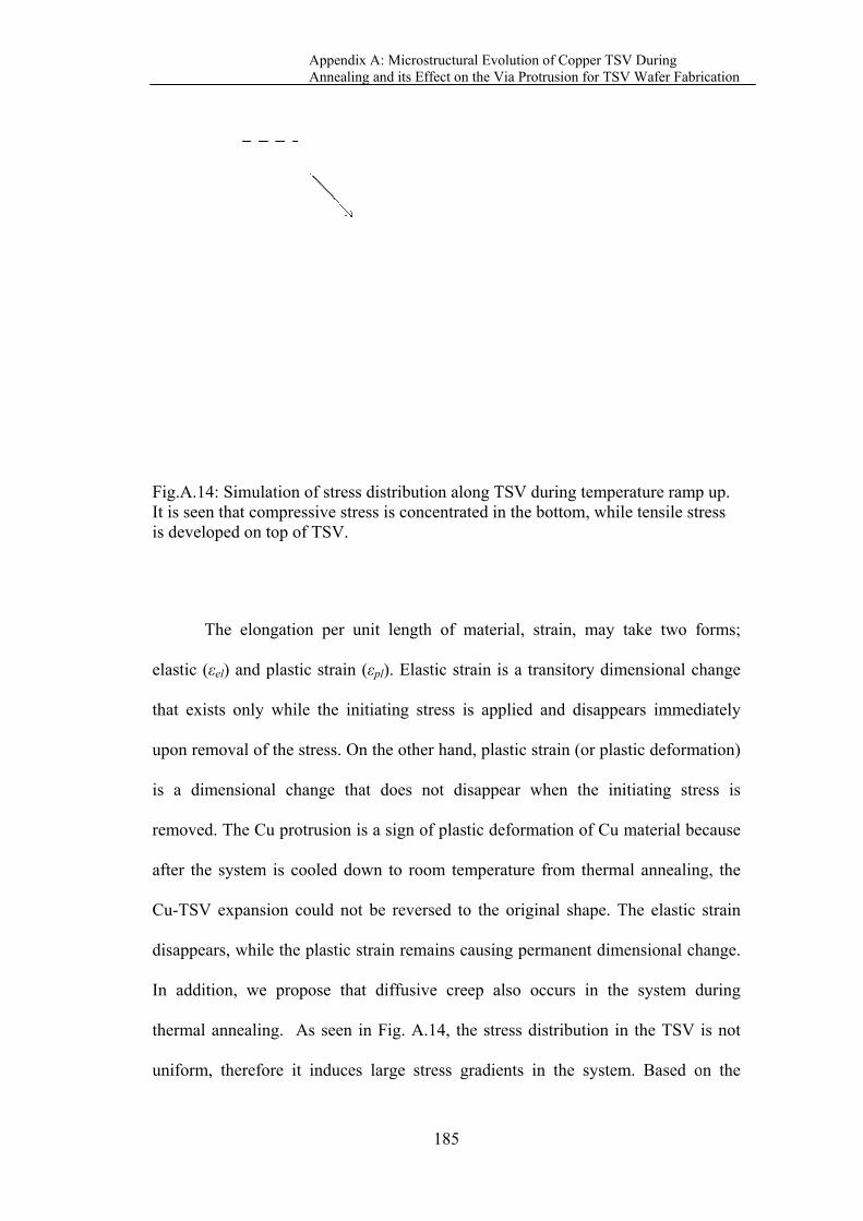
FIi
e
t
u
i
r
a
C
d
I
t
u
Fig.A.14: SiIt is seen thais developed
The
elastic (εel)
that exists o
upon remov
is a dimen
removed. Th
after the sy
Cu-TSV ex
disappears,
In addition,
thermal ann
uniform, th
AA
imulation oat compressd on top of T
elongation
and plastic
only while
val of the str
nsional chan
he Cu protr
stem is coo
xpansion cou
while the p
, we propo
nealing. As
herefore it i
Appendix A: MAnnealing and
of stress distsive stress isTSV.
n per unit l
strain (εpl)
the initiati
ress. On the
nge that do
rusion is a s
oled down t
uld not be
plastic strain
ose that dif
s seen in Fi
induces larg
Microstructurd its Effect on
185
tribution alos concentrat
length of m
. Elastic str
ing stress i
e other hand
oes not di
sign of plast
to room tem
reversed to
n remains c
ffusive cre
ig. A.14, th
ge stress g
al Evolution on the Via Protr
ong TSV duted in the bo
material, str
rain is a tra
s applied a
d, plastic str
sappear wh
tic deforma
mperature f
o the origin
ausing perm
ep also oc
he stress dis
gradients in
of Copper TSVrusion for TSV
uring temperottom, whil
rain, may t
ansitory dim
and disappe
rain (or plas
hen the ini
ation of Cu m
from therma
nal shape. T
manent dim
curs in the
stribution in
the system
V During V Wafer Fabri
rature rample tensile str
take two fo
mensional ch
ears immed
stic deforma
itiating stre
material be
al annealing
The elastic
ensional ch
e system d
n the TSV i
m. Based o
ication
p up. ress
forms;
hange
iately
ation)
ess is
cause
g, the
strain
hange.
during
is not
n the

Appendix A: Microstructural Evolution of Copper TSV During Annealing and its Effect on the Via Protrusion for TSV Wafer Fabrication
186
Nabarro-Herring creep model, the Cu atoms will diffuse from the compressive to
tensile regions, in order to release compressive stress in TSV.
The plastic deformation due to the thermal expansion is clearly shown from
the experimental results (Fig. A.4), in which the amount of Cu protrusion depends
on the temperature. As the thermal load rises, the residual permanent deformation of
the Cu TSV increases. Assuming that in the initial condition, the via volume is V1
and mass density is ρ1, after the first thermal cycle, the via volume will increase due
to protrusion. Since there is an increment in the via volume (V2 > V1), while from
the cross-sectional SEM analysis, there is no void formation in the via, and it means
that the mass density of via decreases (ρ2 < ρ1). This argument is supported by the
nano-indentation measurement, in which the hardness of the annealed TSV is lower
compared to the fresh sample.
After the CMP process, the via volume reverts to the initial volume because
the excess Cu is removed (V3 = V1). It is hypothesized that the Cu protrusion
problem is minimized during the second annealing (Fig. A.11), because the
reduction in the mass density induces a smaller thermal expansion. In addition, due
to the plastic deformation of Cu at the first annealing process, the Cu deformation at
the second annealing is much smaller.
Unfortunately, diffusive creep still occurs due to different stress
concentration along the TSV. As a result, a much smaller Cu protrusion is still
found in the TSV after the second annealing is completed. This diffusive creep
mechanism becomes dominant when the samples are annealed for longer, because
more Cu atoms will diffuse out of the plane to release the compressive stress in
TSV. The AFM characterization, shown in Fig. A.12, supports this hypothesis.

Appendix A: Microstructural Evolution of Copper TSV During Annealing and its Effect on the Via Protrusion for TSV Wafer Fabrication
187
Furthermore, the Cu-protrusion problem will also re-occur if the second
annealing temperature is larger than the preceding annealing process (Fig. A.13),
because a greater thermal load induces a further plastic deformation of the TSV.
Therefore, in order to minimize Cu protrusion effect, the subsequent thermal load
should be less than the initial TANN. The copper annealing after electroplating
process also helps to reduce the diffusive creep, because an increase in the grain
size will degrade the creep mechanism [25]. As shown in Fig. A.5 by the EBSD
measurements, higher annealing conditions result in an increase in the grain size
and thus help to reduce the creep.

Appendix A: Microstructural Evolution of Copper TSV During Annealing and its Effect on the Via Protrusion for TSV Wafer Fabrication
188
Fig.A.15: Schematic diagrams illustrating the Cu protrusion mechanism.
A.4 Summary
We have presented a detailed physical characterization study of the Cu
protrusion effect with its microstructural evolution. It was observed that annealing
a silicon wafer with copper TSVs causes high stresses in the copper and may cause
a “pumping” phenomenon in which the copper is forced out of the blind TSV to
form a protrusion. From the AFM results, the protrusion height increases linearly
with the annealing temperature. Furthermore, EBSD analysis was employed to
study the grain size evolution for different annealing temperatures. It shows that
higher annealing temperature causes an increase in the grain size, due to the grain
growth process. When the sample was annealed from 25 ºC to 450ºC, the
protrusion displacement increased from 36 nm to 958 nm, while the grain size
increased only marginally from 0.84µm to 1.26µm.

Appendix A: Microstructural Evolution of Copper TSV During Annealing and its Effect on the Via Protrusion for TSV Wafer Fabrication
189
Nano-indentation technique was used to study the effect of annealing
temperature with respect to the material properties of Cu-TSV. From the
measurement results, it shows that the hardness, yield strength and elastic modulus
decrease when the samples were annealed at high temperature. The statistical result
shows that the hardness of Cu-TSV dropped to 962 MPa from 1418 MPa, the yield
strength fell to 321 MPa from 473 MPa and the elastic modulus decreased to 91.77
GPa from 116.28 GPa.
Based on these experimental results, we attributed the Cu protrusion
phenomenon to two possible mechanisms. The first mechanism is due to plastic
deformation of Cu material. When the Cu-TSV is heated up, it will expand only
vertically due to lateral constraints by the surrounding Si substrate. If the TSV is
elongated beyond its elastic limit, it will cause a permanent plastic deformation
(irreversible). The second mechanism is due to diffusive creep. As the stress
distribution in the TSV is not uniform, large stress gradients tend to develop across
the TSV and as a result, Cu atoms diffuse from compressive to tensile regions to
achieve stress relaxation and reach lowest system energy configuration.
Therefore, in order to minimize Cu protrusion effect, it is necessary to
anneal the samples after electroplating process with the highest thermal budget to
avoid further plastic deformation. The copper annealing after electroplating process
also helps to reduce the diffusive creep, because an increase in the grain size will
reduce the driving force for creep. However, over long test / operating duration,
diffusive creep still occurs and its cumulative effect could still be a critical
reliability issue, which deserves further in-depth studies.

Appendix A: Microstructural Evolution of Copper TSV During Annealing and its Effect on the Via Protrusion for TSV Wafer Fabrication
190
References
[1] International Technology Roadmap for Semiconductors Report Update 2010. [2] M. Karnezos, F Carson, R Pendse, "3D packaging promises performance,
reliability gains with small footprints and lower profiles,"Chip Scale Review, Vol. 1 (2005), pp. 29.
[3] S. F. Al-Sarawi, D. Abbott, and P. D. Franzon, "A review of 3-D packaging technology," IEEE Transactions on Components, Packaging and Manufacturing Technology, Part B: Advanced Packaging, vol. 21, pp. 2-14, 1998.
[4] R. E. Terrill, "Aladdin: Packaging lessons learned," in Proceedings 1995 International Conference on Multichip Modules (SPIE Vol.2575), 19-21 April 1995, Reston, VA, USA, 1995, pp. 7-11.
[5] K. Takahashi, H. Terao, Y. Tomita, Y. Yamaji, M. Hoshino, T. Sato, T. Morifuji, M. Sunohara, and M. Bonkohara, "Current status of research and development for three-dimensional chip stack technology," Japanese Journal of Applied Physics, Part 1: Regular Papers and Short Notes and Review Papers, vol. 40, pp. 3032-3037, 2001.
[6] P. Ramm, D. Bollmann, R. Braun, R. Buchner, U. Cao-Minh, M. Engelhardt, G. Errmann, T. Grassl, K. Hieber, H. Hubner, G. Kawala, M. Kleiner, A. Klumpp, S. Kuhn, C. Landesberger, H. Lezec, W. Muth, W. Pamler, R. Popp, E. Renner, G. Ruhl, A. Sanger, U. Scheler, A. Schertel, C. Schmidt, S. Schwarzl, J. Weber, and W. Weber, "Three dimensional metallization for vertically integrated circuits," in Second European Workshop on Materials for Advanced Metallization. MAM'97, 16-19 March 1997, Netherlands, 1997, pp. 39-47.
[7] M. Koyanagi, H. Kurino, K. Lee, K. Sakmicrona, N. Miyakawa, H. Itani, "Future System-on-Silicon LSI Systems," IEEE Micro, Vol. 18, No. 4 (1998), pp 17-22.
[8] K. Takahashi et. al., "Development of Advanced 3-D Chip Stacking Technology with Ultra-Fine Interconnection," Proc 51fh Electronic Components and Technology Conf, Orlando, FL, May. 2001, pp. 541-546.
[9] G. Feng, X. Peng, J. Cai, and S. Wang, "Through wafer via technology for 3-D packaging," in 2005 6th International Conference on Electronics Packaging Technology, August 30, 2005 - September 2, 2005, Dameisha, Shenzhen, China, 2005, pp. CIE-CEPS..
[10] P. Garrou “Researchers Strive for Copper TSV Reliability” Semiconductor International, Dec 2009
[11] S. E. Thompson, S. Guangyu, C. Youn Sung, and T. Nishida, "Uniaxial-process-induced strained-Si: extending the CMOS roadmap," IEEE Transactions on Electron Devices, vol. 53, pp. 1010-20, 2006.
[12] K. H. Lu, R. Suk-Kyu, Z. Qiu, Z. Xuefeng, J. Im, H. Rui, and P. S. Ho, "Thermal Stress Induced Delamination of Through Silicon Vias in 3-D Interconnects," in IEEE 60th Electronic Components and Technology Conference (ECTC 2010), 1-4 June 2010, Piscataway, NJ, USA, 2010, pp. 40-5.
Appendix A: Microstructural Evolution of Copper TSV During Annealing and its Effect on the Via Protrusion for TSV Wafer Fabrication
191
[13] J. Van Olmen, J. Coenen, W. Dehaene, K. De Meyer, C. Huyghebaert, A. Jourdain, G. Katti, A. Mercha, M. Rakowski, M. Stucchi, Y. Travaly, E. Beyne, and B. Swinnen, "3D stacked IC demonstrator using Hybrid Collective die-to-wafer bonding with copper Through Silicon Vias (TSV)," in 2009 IEEE International Conference on 3D System Integration (3DIC), 28-30 Sept. 2009, Piscataway, NJ, USA, 2009, p. 5.
[14] C. Okoro, C. Huyghebaert, J. Van Olmen, R. Labie, K. Lambrinou, B. Vandevelde, E. Beyne, and D. Vandepitte, "Elimination Of The Axial Deformation Problem Of Cu-TSV In 3D Integration," AIP Conference Proceedings, vol. 1300, pp. 214-220, 2010.
[15] Wyko Surface Profilers Technical Reference Manual, p 1-1-14. [16] S.H. Rhee, D. Yong, and P. S. Ho, "Thermal stress characteristics of Cu/oxide
and Cu/low-k submicron interconnect structures," Journal of Applied Physics, vol. 93, pp. 3926-33, 2003.
[17] M. Murakami, T.-S. Kuan and I. A. Blech, Preparation and Properties of Thin Films (Treatise on Materials Science and Technology, Vol.24), pp.163-210, 1982.
[18] H. Lee, S.S. Wong, S.D. Lopatin, “Correlation of stress and texture evolution during self and thermal annealing of electroplated Cu films”, Journal of Applied Physics, vol. 93, pp. 3796-3804, 2003.
[19] C. Okoro, R. Labie, K. Vanstreels, A. Franquet, M. Gonzales, B. Vandevelde, E. Beyne, D. Vandepitte, B. Verlinden, “Impact of the electrodeposition chemistry used for TSV filling on the microstructual and thermo-mechanical response of Cu”, Journa; of Mateial Science,Vol. 46, pp. 3868-82, 2011.
[20] W. C. Oliver and G. M. Pharr, J. Mater. Res. 7, 1564, 1992. [21] T. H. Courtney, Mechanical Behavior of Materials (McGrill-Hill, New York,
NY, 1990), pp. 80–136, and 263–324. [22] W.D. Nix and H.J. Gao 1998 J. Mech. Phys. Solids [23] R. E. Kumon and D. C. Hurley, "Effects of residual stress on the thin-film
elastic moduli calculated from surface acoustic wave spectroscopy experiments," Thin Solid Films, vol. 484, pp. 251-6, 2005.
[24] A.S. Budiman, “Orientation and Stress Mapping in Post-Annealed and in situ Heating of Cu Through-Silicon Via (TSV) Samples using Synchrotron-based X-ray Microdiffraction”, IEEE Singapore Rel/CPMT/ED Chapter technical talk, November 2010.
[25] G. B. Alers, J. Sukamto, P. Woytowitz, X. Lu, S. Kailasam, and J. Reid, "Stress migration and the mechanical properties of copper," in 2005 IEEE International Reliability Physics Symposium. Proceedings 43rd Annual, 17-21 April 2005, Piscataway, NJ, USA, 2005, pp. 36-40.

Appendix B: Resistance Degradation Trends
192
APPENDIX B
Resistance Degradation Trends
The resistance degradation and sorted data on the TTF in the main chapters are
shown in this part.
Chapter 4
Figure 4.8
No. TTF (Hours)
Normal Dielectric Slot 1 12.41 13.89 2 18.48 16.96 3 23.54 18.78 4 24.75 26.63 5 26.77 29.25 6 30.84 31.25 7 32.01 31.34 8 36.14 34.36 9 42.46 41.1
10 43.38 41.64 11 47.13 43.2 12 47.38 45.15 13 47.93 47.09 14 50.72 47.91 15 55.88 51.21 16 55.91 53.07 17 59.8 55.04 18 67.07 56.91 19 67.67 62.09 20 71.35 69.72 21 75.4 70.05 22 76.02 76.1 23 77.24 81.27
Sample size 23 23

Appendix B: Resistance Degradation Trends
193
Fig.B.1. Resistance-time degradation trends for (a)normal and (b)dielectric slot structure.
Chapter 5 Figure 5.4
The typical resistance trends for both FM-I and FM-II groups of the
SM+EM samples show a catastrophic resistance shoot-up trend, as seen in Figure
B.2, where open-circuit failures occur abruptly. On the other hand, the resistance
trend for the majority of the control sample is a staircase-like gradually increasing
(a)
(b)

Appendix B: Resistance Degradation Trends
194
trace which indicates that multiple, small random voids in the via-chain structure
nucleate and grow (Fig.B.3).
No Time (Hours)
SM+EM EM-test only 1 38.08 70.4 2 41.75 71.09 3 42.18 71.75 4 43.32 72.44 5 44.31 72.58 6 44.4 79.13 7 55.08 82.31 8 55.94 83.08 9 57.22 88.9
10 58.06 94.07 11 58.72 96.48 12 58.94 97.37 13 60.43 99.87 14 61.39 100.84 15 63.65 107.31 16 63.76 108.85 17 64.87 111.02 18 65.5 112.82 19 66.37 119.5 20 69.47 121.11 21 69.63 124.92 22 69.75 130.87 23 71.87 137.29 24 72.69 25 77.88 26 79.48 27 82.2 28 87.02 29 101.76 30 119.36 31 125.81 32 159.45
Sample size 32 23

Appendix B: Resistance Degradation Trends
195
Fig.B.2. Resistance-time degradation trends for SM+EM test in lower interconnect. It shows that most of the samples (FM-1 and FM-II) under SM+EM test show abrupt resistance jump which indicates that a fatal void is formed.
Fig.B.3. (a) Resistance-time degradation trends for the “EM-test only” samples. It shows that most of the samples have a step-like resistance characteristic which indicates occurrence of multiple failures. (b) Focusing on the observed trend in one of the degraded samples in (a).

Appendix B: Resistance Degradation Trends
196
Figure 5.6
No Time (Hours)
SM+EM EM-test only 1 87.34 90.02 2 88.68 95.18 3 93.35 96.55 4 96.51 103.41 5 99.61 107.18 6 100.65 110.05 7 105.43 112.04 8 107.29 113.33 9 109.34 114.49 10 109.72 116.64 11 117.31 118.93 12 119.23 119.52 13 119.97 122.1 14 125.71 129.43 15 126.16 130.45 16 127.2 131.45 17 136.2 18 139.52 19 146.32 20 154.75 21 156.84
Sample size 16 21
Fig.B.4. Resistance-time degradation trends for SM+EM test and EM test-only in upper interconnect.

Appendix B: Resistance Degradation Trends
197
Chapter 6
Figure 6.1
No
300°C 325°C Time (Hours) Time (Hours)
SM+EM EM-test
only SM+EMEM-test
only 1 194 298 80.2 117 2 197 313 103 122 3 201 322 107 138 4 217 329 115 154 5 229 343 145 157 6 285 371 167 174 7 322 374 174 186 8 336 397 176 194 9 361 398 191 196
10 364 441 197 204 11 365 197 233 12 383 202 251
Sample Size 12 10 12 12
Figure 6.3
No
0.6MA/cm2 1MA/cm2 Time (Hours) Time (Hours)
SM+EM EM-test
only SM+EM EM-test only 1 146 105 52.4 61 2 164 179 59.4 64.4 3 174 187.02 67.5 67.8 4 188 222 75.6 68.2 5 195 225 76.7 69.3 6 196 229 79 70.2 7 197 233 80.2 72.1 8 200 240 80.8 72.3 9 238 243 82.4 77.4
10 239 246 86.3 79.8 11 241 250 91 81.9 12 244 258 94.6 83.3 13 261 96.8 88 14 262 90.6 15 275 91.4 16 282
Sample Size 12 16 13 15

Appendix B: Resistance Degradation Trends
198
Figure 6.9
No. Time (Hours)
SM+EM EM-test
only 1 122.7 131.7 2 131.8 135.3 3 135.2 135.3 4 136.4 136.3 5 138.9 139.1 6 141.7 140.6 7 142.9 141.7 8 144.9 144.3 9 146.9 150.7
10 148.3 154.4 11 154.8 161 12 155.9 171.5 13 158.1 174.8 14 163.33 179.5 15 165.6 191.2 16 166.4 192.2 17 166.8 200 18 172.1 19 172.3 20 172.9 21 173 22 173.1 23 180.2 24 188.1
Sample Size 24 17
The resistance trend is similar with Figs.B.2 and B.3.

Appendix B: Resistance Degradation Trends
199
Chapter 7
Figure 7.2
No. Fig.7.2(a) Fig.7.2(b)
Time (Hours) Time (Hours) SM+EM EM-test only SM+EM EM-test only
1 3.32 3.27 49.82 54.51 2 3.33 3.47 55.23 68.38 3 3.54 4.3 62.36 77.92 4 3.69 4.34 62.58 89.81 5 3.83 4.8 68.55 99.9 6 3.9 5.4 70.56 102.49 7 3.91 5.89 72.29 112.06 8 4.04 6.5 72.67 119.54 9 4.11 7.67 82.02 140.54
10 4.25 8.14 89.31 143.82 11 4.54 9.4 91.69 148.84 12 4.89 12.9 92.4 13 4.89 12.97 99.17 14 4.97 14.9 104.71 15 5.42 18.8 105.25 16 5.67
17 5.81
18 6.15
Sample Size 15 18 15 11
Fig.B.5: Resistance degradation of SM+EM test and EM test-only for narrow advanced interconnects.

Appendix C: Procedure to determine Ea and n
200
APPENDIX C
Procedure to determine Ea and n
The block diagram showing the procedure to determine Ea and n is shown below.
50 exp an
EAt
j kT
50
1ln lna n
At E
kT j
50ln ln ln aEt n j A
kT
Select 3 stress temperatures and 3 stress current densities.
Conduct experiment to
obtain TTF
Construct log-normal
probability plot to obtain t50.
Plot lnt50 against 1/kT and ln(1/j)
separately to determine Ea and n
respectively
Black’s Equation
Obtain linear equation