Effect of Nanoscale Patterned Interfacial Roughness on
87
SANDIA REPORT SAND2007-5990 Unlimited Release Printed September 2007 Effect of Nanoscale Patterned Interfacial Roughness on Interfacial Toughness E. D. Reedy, Jr., N. R. Moody, J. A. Zimmerman, X. Zhou, M. S. Kennedy, W. M. Mook, D. F. Bahr Prepared by Sandia National Laboratories Albuquerque, New Mexico 87185 and Livermore, California 94550 Sandia is a multiprogram laboratory operated by Sandia Corporation, a Lockheed Martin Company, for the United States Department of Energy’s National Nuclear Security Administration under Contract DE-AC04-94AL85000. Approved for public release; further dissemination unlimited.
Transcript of Effect of Nanoscale Patterned Interfacial Roughness on

SANDIA REPORT SAND2007-5990 Unlimited Release Printed September 2007
Effect of Nanoscale Patterned Interfacial Roughness on Interfacial Toughness E. D. Reedy, Jr., N. R. Moody, J. A. Zimmerman, X. Zhou, M. S. Kennedy, W. M. Mook, D. F. Bahr Prepared by Sandia National Laboratories Albuquerque, New Mexico 87185 and Livermore, California 94550 Sandia is a multiprogram laboratory operated by Sandia Corporation, a Lockheed Martin Company, for the United States Department of Energy’s National Nuclear Security Administration under Contract DE-AC04-94AL85000. Approved for public release; further dissemination unlimited.

2
Issued by Sandia National Laboratories, operated for the United States Department of Energy by Sandia Corporation. NOTICE: This report was prepared as an account of work sponsored by an agency of the United States Government. Neither the United States Government, nor any agency thereof, nor any of their employees, nor any of their contractors, subcontractors, or their employees, make any warranty, express or implied, or assume any legal liability or responsibility for the accuracy, completeness, or usefulness of any information, apparatus, product, or process disclosed, or represent that its use would not infringe privately owned rights. Reference herein to any specific commercial product, process, or service by trade name, trademark, manufacturer, or otherwise, does not necessarily constitute or imply its endorsement, recommendation, or favoring by the United States Government, any agency thereof, or any of their contractors or subcontractors. The views and opinions expressed herein do not necessarily state or reflect those of the United States Government, any agency thereof, or any of their contractors. Printed in the United States of America. This report has been reproduced directly from the best available copy. Available to DOE and DOE contractors from U.S. Department of Energy Office of Scientific and Technical Information P.O. Box 62 Oak Ridge, TN 37831 Telephone: (865) 576-8401 Facsimile: (865) 576-5728 E-Mail: [email protected] Online ordering: http://www.osti.gov/bridge Available to the public from U.S. Department of Commerce National Technical Information Service 5285 Port Royal Rd. Springfield, VA 22161 Telephone: (800) 553-6847 Facsimile: (703) 605-6900 E-Mail: [email protected] Online order: http://www.ntis.gov/help/ordermethods.asp?loc=7-4-0#online

3
SAND2007-5990 Unlimited Release
Printed September 2007
Effect of Nanoscale Patterned Interfacial Roughness on Interfacial Toughness
E. David Reedy, Jr.
Applied Mechanics Development
Neville R. Moody Analytical Materials Science
Jonathan A. Zimmerman, and Xiaowang Zhou
Mechanics of Materials
Sandia National Laboratories P.O. Box 5800
Albuquerque, NM 87185-0346
Marian S. Kennedy Clemson University Clemson, SC 29634
William M. Mook
University of Minnesota Minneapolis, MN 55455
David F. Bahr
Washington State University Pullman, WA 99164
Abstract
The performance and the reliability of many devices are controlled by interfaces between thin films. In this study we investigated the use of patterned, nanoscale interfacial roughness as a way to increase the apparent interfacial toughness of brittle, thin-film material systems. The experimental portion of the study measured the interfacial toughness of a number of interfaces with nanoscale roughness. This included a silicon interface with a rectangular-toothed pattern of 60-nm wide by 90-nm deep channels fabricated using nanoimprint lithography techniques. Detailed finite element simulations were used to investigate the nature of interfacial crack growth when the interface is patterned. These simulations examined how geometric and material parameter choices affect the apparent toughness. Atomistic simulations were also performed with the aim of identifying possible modifications to the interfacial separation models currently used in nanoscale, finite element fracture analyses. The fundamental nature of atomistic traction-separation for mixed mode loadings was investigated.

4

5
Table of Contents
1. Introduction....................................................................................................10 2. Experiments Investigating the Effect of Nanoscale Roughness.....................11
2.1 Introduction .......................................................................................11 2.2 Surface Chemistry Effects on Adhesion............................................12
2.2.1 Materials and Procedure ....................................................12 2.2.2 Results and Discussion.......................................................13 2.2.3 Fracture Energy Analysis ....................................................13
2.3. Linear Channel Pattern Effects on Adhesion ...................................16 2.3.1 Materials and Procedure .....................................................16 2.3.2 Results and Discussion.......................................................17
2.4 Roughened Surface Effects on Adhesion .........................................17 2.4.1 Lapped silicon substrates....................................................18
2.4.1.1 Materials and Procedure .......................................18 2.4.1.2 Results ..................................................................18
2.4.2 Hillock Roughening .............................................................18 2.4.2.1 Materials and Procedure .......................................19 2.4.2.2 Results and Discussion .........................................19
2.4.3 Continuing Work..................................................................20 2.5 Summary ..........................................................................................20 2.6 References .......................................................................................21
3. Finite Element Analysis of Cracking Along a Patterned Interface..................37 3.1 Introduction .......................................................................................37 3.2 Finite Element Simulations ...............................................................37 3.3 Results..............................................................................................39 3.4 Discussion ........................................................................................41 3.5 Conclusions ......................................................................................43 3.6 References .......................................................................................44
4. Molecular Dynamics Simulations of Interfacial Separation ............................57 4.1 Introduction .......................................................................................57 4.2 Simulation approach .........................................................................58
4.2.1 Interatomic potentials for bcc metals ..................................59 4.2.2 Interatomic potentials for brittle interfaces...........................61 4.2.3 Molecular dynamics model .................................................61
4.3 Results.............................................................................................63 4.3.1 Global stress strain curve....................................................63 4.3.2 Crack propagation dynamics...............................................65 4.3.3 Spatial distribution of stress and crack opening ..................65 4.3.4 Observation of stress as a function of crack opening..........66 4.3.5 Analytical expressions for stress vs. crack opening ............66
4.4 Conclusions ......................................................................................68 4.5 References .......................................................................................69
5. Summary .......................................................................................................85

6
List of Figures
Fig. 2.1. (a) This image shows the uniform deposition of the polymer tubes. (b)
Closer examination shows very uniform tubes were deposited with a
diameter of 200 nm. (c) A tilted sectional view shows that the tubes stand
approximately 500 nm high. ................................................................................ 25
Fig. 2.2. The telephone cord buckles formed spontaneously when the 250nm
compressive W film delaminated from the oxidized silicon substrate................... 26
Fig. 2.3. AFM images were taken of the buckles that formed during the
separation of the tungsten-oxidized silicon interface and this is a typical
cross section ....................................................................................................... 26
Fig. 2.4a. Straight walled buckles formed spontaneously on the polymer patterned
samples with some short telephone cord buckle formation................................... 27
Fig. 2.4b. Cross section of the buckle morphology seen in delamination along
tungsten-oxidized silicon interface masked by polymer tubes. ............................. 27
Fig. 2.5. This image of the under side of the W film after delamination shows the
pores made during deposition and the polymer tubes within these pores. ............ 28
Fig. 2.6. A cross section schematic showing dimensions of a uniform width
straight wall and telephone cord buckle. ............................................................ 28
Fig. 2.7. Nanoimprint lithography was used to create two dimensional
rectangular-toothed patterns (i.e., parallel channels with a rectangular cross-
section) in silicon wafer substrates as shown here for the 200 nm pitch
sample ................................................................................................................. 29
Fig. 2.8. Reentrant corners at the base of the 500 nm pitch sample channels
exhibited significantly more rounding than the 100 nm pitch sample channel
corners................................................................................................................. 29
Fig. 2.9. Sputter deposition onto the 500 nm pitch channel samples was
unidirectional with partial channel fill. The films completely filled the base
of the channels and channel corners. .................................................................... 30

7
Fig. 2.10. Films on the 500 nm pitch channel pattern surface were uniform in
thickness and delaminated following deposition. Residual stresses led to
film roll. .............................................................................................................. 30
Fig. 2.11. Deposition of a thicker film on the 500 nm pitch samples led to
widespread coil formation as the tungsten films delaminated from the
channel pattern surface. ....................................................................................... 31
Fig. 2.12. The films spontaneously delaminated following deposition forming two
types of buckles. (a) Small telephone-cord like buckles formed on the
channel patterns by alternating segments running parallel and perpendicular
to the channels. (b) Large straight-sided buckles formed perpendicular to the
channel patterns................................................................................................... 32
Fig. 2.13. Optical micrographs showing silicon substrates with (a) 2 nm rms and
(b) 912 nm rms surface roughness. The inserts are AFM deflection images
of the substrate surfaces....................................................................................... 33
Fig. 2.14. Scratch test of tungsten on smooth silicon shows a distinct transition
when film fracture occurs. ................................................................................... 34
Fig. 2.15. The rough morphology prevents uniform loading of external stresses
into the film system as shown by this plot of lateral and normal loading into
the tungsten film on rough silicon........................................................................ 34
Fig. 2.16. The silicon substrates were fabricated using deep reactive ion etching
leading to silicon grass formation. ....................................................................... 35
Fig. 2.17. Removing the silicon grass leaves a roughened surface................................. 35
Fig. 2.18. (a) Schematic of a multilayer film sample showing loads and moments
in flexure during (b) four-point bend testing. ....................................................... 36
Fig. 3.1. Traction-separation relationship used in finite element calculations. ............... 48
Fig. 3.2. Geometry of film on a patterned substrate model analyzed (2a). Both
rectangular and rippled channel interface patterns considered (2b and 2c)........... 48
Fig. 3.3. Calculated interfacial traction as a function of applied edge loading when
!
ˆ " =300 MPa. ....................................................................................................... 49
Fig. 3.4. Calculated interfacial traction as a function of applied edge loading when
!
ˆ " =400 MPa. ....................................................................................................... 50

8
Fig. 3.5. Calculated interfacial traction as a function of applied edge loading
when
!
ˆ " =600 MPa. ............................................................................................. 51
Fig. 3.6. Calculated interfacial traction as a function of applied edge loading when
!
ˆ " =800 MPa. ....................................................................................................... 52
Fig. 3.7. Calculated interfacial traction as a function of applied edge loading when
!
ˆ " =1000 MPa....................................................................................................... 53
Fig. 3.8. Calculated interfacial traction as a function of applied edge loading when
!
ˆ " =1200 MPa....................................................................................................... 54
Fig. 3.9. The normalized apparent toughness as a function of the global mode
mixity.................................................................................................................. 55
Fig. 3.10. Normalized apparent toughness as a function of the ratio of interfacial
strength-to-segment cracking stress. .................................................................... 56
Fig. 4.1. Pair energy function curves for different pairs. ............................................... 72
Fig. 4.2. Cohesive energy as a function of lattice constant ............................................ 72
Fig. 4.3. Geometry of molecular dynamics simulation. ................................................. 73
Fig. 4.4. Shear loading boundary conditions. ................................................................ 74
Fig. 4.5. Schematic of regions used to calculate (a) global and (b) local properties. ...... 75
Fig. 4.6. Tensile stress as a function of (a) true normal strain; and (b) normal
boundary displacement obtained under pure tensile loading condition θ = 0◦........ 76
Fig. 4.7. Shear stress as a function of (a) shear strain; and (b) shear boundary
displacement obtained under pure shear loading condition θ = 90◦ . ..................... 77
Fig. 4.8. Crack length as a function of time. ................................................................. 78
Fig. 4.9. Stress and opening as functions of x coordinate obtained at a mixed
loading condition of θ = 45◦. (a) normal stress and normal opening; and (b)
shear stress and shear opening. ............................................................................ 79
Fig. 4.10. (a) local normal stress as a function of crack local normal opening
under mode I fracture; and (b) local shear stress as a function of crack local
shear opening under mode II fracture................................................................... 80
Fig. 4.11. Comparison of the σp, rp, α, and β MD data with analytical prediction.
(a) σp; (b) α; (c) rp; and (d) β. .............................................................................. 81
Fig. 4.12. Comparison of stress σ as a function of crack opening Δr between MD
9
data and fitted curves.................................................................................................... 82
Fig. 4.13. Stress σ as a function of crack opening components Δx and Δy. ................... 83
Fig. 4.14. Work of separation as a function of loading condition ψ................................84
List of Tables
Table 2.1. Fracture energies for sputter deposited tungsten on smooth and
polymer patterned oxidized silicon wafer............................................................. 24
Table 2.2. Fracture energies for sputter deposited tungsten on smooth and channel
patterned oxidized silicon wafers. ........................................................................ 24
Table 3.1. Illustrative finite element results demonstrating the accuracy and
convergence of calculated apparent toughness Γa................................................. 45
Table 3.2. Apparent toughness Γa as a function of interfacial strength
!
ˆ " . ..................... 45
Table 3.3. Apparent toughness Γa as a function of substrate material. ........................... 45
Table 3.4. Apparent toughness Γa as a function of intrinsic interfacial toughness
Γo. ....................................................................................................................... 46
Table 3.5. Apparent toughness Γa as a function of characteristic length a. .................... 46
Table 3.6. Apparent toughness Γa as a function of channel pattern aspect ratio b/a ....... 46
Table 3.7. Apparent toughness Γa as a function of film thickness h............................... 47
Table 3.8. Apparent toughness Γa as a function of the global mode mixity.................... 47
Table 3.9. Apparent toughness Γa as a function of type of interfacial channel
pattern. ................................................................................................................ 47
Table 4.1. Pair potential parameters.............................................................................. 70
Table 4.2. Predicted equilibrium lattice constant a, cohesive energy Ec, bulk
modulus B, elastic moduli C’ and C44, (110) surface energy γ, and (110)
crack brittleness ρ, of the three bcc crystals. ........................................................ 70
Table 4.3. Boundary displacement rates X&! and Y&! , strain rates xy!& and
yy!& ,
and loading angle θ.............................................................................................. 71
Table 4.4. Cohesive zone model parameters. ................................................................ 71

10
1. Introduction
The performance and the reliability of many devices are controlled by interfaces between thin films. The toughness of such interfaces is, however, often quite low because there is little energy dissipation in the surrounding bulk materials. Consequently, there is a clear need for techniques to engineer thin film interfaces with improved toughness in order to enhance thin film performance and reliability. The goal of this LDRD-funded project was to determine if patterned, nanoscale interfacial roughness could be used to significantly increase the apparent interfacial toughness of brittle, thin-film material systems. The approach to accomplish this goal included three primary tasks. First we performed a series of well-defined experiments to measure the toughness of interfaces with nanoscale roughness. This included tests of patterned interfaces generated using a commercially available, thermal nanoimprint lithography (T-NIL) tool. T-NIL can nano-pattern large areas by stamping a high precision master pattern into a polymer resist coating that is then etched to transfer the pattern to the underlying silicon wafer. This technique was used to create a rectangular-toothed pattern of 60-nm wide by 90-nm deep channels on a silicon surface. A highly compressed tungsten film is sputter deposited on top of the patterned silicon interface to create thin film systems for testing. Chapter 2 of this report describes the details of the experimental portion of the project. We also performed detailed finite element crack growth simulations to determine how geometric and material parameter choices affect the apparent toughness of interfaces with patterned nano-scale roughness. Calculations were performed for the idealized problem of a thin, bimaterial strip loaded by displacing the top edge relative to the bottom edge. An explicit, transient dynamics finite element code was used for the analysis since this type of code is well suited for analyzing discontinuous crack growth. Interfacial separation was simulated using a cohesive zone model. The fundamental parameters used to define the cohesive zone traction-separation relationship are interfacial strength and the intrinsic work of separation/unit area. Chapter 3 describes the details of the modeling approach as well as key findings. The aim of the third task was to use atomistic simulations to suggest modifications to the interfacial separation models currently used in nanoscale, finite element fracture analyses. The fundamental nature of atomistic traction-separation for mixed mode loadings was investigated. This work is discussed in Chapter 4.

11
2. Experiments Investigating the Effect of
Nanoscale Roughness
2.1 Introduction Thin films are used in many applications where their properties are needed to meet specialized functional requirements.1 These properties include resistance to abrasion, corrosion, permeation and oxidation, or special magnetic and dielectric properties. Thin films uses are steadily growing due to surges in both micro and nanoelectromechanical systems (MEMS and NEMS),2,3 where they are used to optimizing performance of small volume systems. In addition, innovations in film material selections are helping to reinvigorate established microelectronic markets. An example of this is the emergence of copper as the next generation interconnect metallization material for ultra-large-scale integration (USLI).4 In all thin film applications, reliability and durability are tied directly to the structure and composition of the interface between the film and its substrate.1,5,6 The properties of an interface are a function of the dissimilarities of the joined materials. This dissimilar nature, such as differences in residual stress, structure, and composition, can create significant challenges for the mechanical integrity and reliability.7 Mismatches in thermal coefficients of the interface materials and high energy deposition techniques can create film systems with high residual stress levels capable of driving fracture along interfaces. Differences in structure and composition can markedly alter interface adhesion and strength. In brittle films, friction along contacting crack faces can increase performance while in ductile films plastic deformation can markedly increase fracture energy.7,8 Fracture processes can also have a strong effect on device performance. In brittle film systems, debonding can occur by rupture of bonds along the interface plane at relatively low fracture energies.7,9 When brittle interphases or reaction products form, fracture can occur also within these phases and reaction products at relatively low fracture energies. In contrast, hole nucleation, growth, and coalescence can markedly increase fracture energies in ductile film systems.7,10,26 In most applications, system size does not limit the design and different processing techniques can be used to improve reliability. Three common examples of processing design improvements are interlayers, film thickness and interface roughness. The interlayers act as barriers to diffusion, segregation, and phase formation and to promote adhesion between a film and a substrate.11,12,13,14,15 Another design criteria that can be altered is the film’s thickness which can be increased to promote ductility and energy dissipation.2,16,17 Roughened interfaces have increased surface area and crack path tortuosity.18,19,20,21,22,23,24,25 However, use of these techniques becomes limited as films approach the nanoscale. Nevertheless, patterning surface chemistry and topography at the nanoscale hold significant promise for increasing film performance and reliability through tailoring resistance to interfacial fracture.
12
Several techniques exist to quantify the interfacial fracture energy, or adhesion energy, of thin films on substrates and are used in this study.26 These techniques include scratch testing,27,28,29,30 four point bending, 31,32,41 indentation, 33,34 and stressed overlayers.34,35,36,37,38 The experimental portion of this study was conducted in three stages to define the effects of interlayers, film thickness and roughness. The discussion of each of is contained in separate sections. The first section discusses the effect of tailored interfacial chemistry on adhesion. The second section discusses use of unidirectional nanopatterns. The third section discusses the effects of uniform nanoscale roughness.
2.2 Surface Chemistry Effects on Adhesion The true work of adhesion, ΓA, is the thermodynamic work required to create two new surfaces at the expense of the interface and is an intrinsic property of a given system that depends on the type of chemical bonding between the film and substrate. ΓA is the summation of the surface energy of the film, γf, and the surface energy of the substrate, γs, minus the interfacial energy of the two materials in contact, γfs. Since the true work of adhesion is influenced by the initial surface energies of the film and substrate, any alteration of these energies will impact the total adhesion energy of the interface. This section looks at the effect of changes in the surface chemistry from polymer patterning on total adhesion energy. 2.2.1 Materials and Procedure
The tungsten on (001) silicon film-substrate system was chosen for this study since it is a well characterized, rigid, elastic, system that can easily be fabricated using DC magnetron sputtering with high compressive stresses. Prior to deposition, all substrates were cleaned using an acetone/IPA/H2O/acetone/IPA rinse process. One set of Si substrates was kept in the as-polished condition to create a smooth interface baseline for comparison. The other set of substrates was patterned with polymer tubes through the use of controlled plasma etching using a South Bay Technology PE-2000 reactive ion etcher. While keeping the ratio of CF4 to O2 at 4:1, oxygen was introduced into the reaction chamber containing the substrates until the pressure reached 20 mTorr.39,40 This created a uniform array of polymer tubes, often referred to as polymer “grass” or “tube worms”,40 across the substrate surface as shown in Fig. 2.1a. Closer examination, Fig. 2.1b and 2.1c, showed that the tubes had a diameter of approximately 200 nm near the top and a base that broadened where it met the substrate.39,40 A 250 nm compressive tungsten film was then deposited onto the smooth silicon substrates using DC magnetron sputtering. A thicker compressive tungsten film was deposited onto the polymer patterned substrates to make sure that the tubes were completely covered by the W film. The compressive stresses in the film served to trigger spontaneous buckle delaminations from which fracture energies were determined. These delamination morphologies were measured with an Autoprobe CP Scanning Probe Microscope in the atomic force microscopy (AFM) mode and inspection of the fracture

13
surface of the polymer-masked interface was carried out using a FEI Sirion scanning electron microscope (SEM). Coverage of the polymer patterns was determined by analyzing SEM images with the image processing software Image SXM. 2.2.2 Results and Discussion Telephone cord buckles with some straight-wall segments formed spontaneously on the smooth substrate samples following tungsten deposition. A typical telephone cord buckle that formed on these samples is shown in Fig. 2.2 with a buckle profile shown in Fig. 2.3. After characterizing the buckle profiles, the film was partially removed allowing the tungsten film thickness of 250 nm to be determined.39,40 Large straight-sided Euler buckles, Fig. 2.4a, formed spontaneously on the polymer patterned silicon substrates following tungsten deposition. A cross section of a buckle taken with AFM, Fig. 2.4b, shows that the tungsten film followed the surface morphology of the polymer patterned substrate. The tungsten film maintained the same hillocky appearance following delamination. After characterizing the buckle profiles, the film was partially removed allowing the tungsten film thickness of 280 nm to be determined. SEM images of the delaminated interface showed that the tubes were pulled from the Si substrate surface. The underside of the tungsten film, the side where the tungsten film was adhered to the polymer patterned substrate, is shown in Fig. 2.5. This image shows that many of the tubes were still embedded in the tungsten film after delamination. The image clearly shows that the tubes are wider in diameter at the base with a base diameter of approximately 310 nm. The total area fraction of silicon covered by the polymer tubes was approximately 22%.39,40 2.2.3 Fracture Energy Analysis Several research groups have been working on methods to explain the formation of different delamination morphologies and to determine the best methods of adhesion calculations. There are currently two methods used to model telephone cord buckles; modeling the buckle as a pinned circular blister43 or modeling as a straight walled buckle.37,44 The mechanics for both methods are available and well understood.43,45 Although many groups agree on the film stress state to form circular blisters (equal biaxial stresses), they do not agree on the stresses required to form wavy buckles. Colin et al.42 monitored 304L stainless steel films on polycarbonate films and saw the evolution from pre-existing straight buckles to wavy buckles. During the transition, the buckles increased in width. This growth in width correlated with the release of stress in the transverse direction and indicated that this is energetically favorable for stresses along the length of the buckles.40 Cordill38 and Kennedy40 have shown that the differences in values from the methods available are well within typical standard deviations. The telephone cord and straight wall buckles provide the data from which interfacial fracture energies can be obtained using solutions for film systems where residual stresses dominate fracture behavior. The interfacial fracture energies for both morphologies are determined following the analysis of Hutchinson and Suo45 for a one-dimensional or

14
straight wall buckle. The analysis is based on the assumption that the film and substrate are elastic isotropic solids, the film is subject to a uniform, equi-biaxial compressive in-plane stress, and the film thickness is much less than the buckle width. The buckle is then modeled as a wide, clamped Euler column of length 2b as shown in Fig. 2.6. For a blister to form in the as-deposited film under these conditions, the compressive residual stress, σr, must exceed the stress for delamination, σb, as follows,45
!
"b =#2E
12 1$ %2&
' (
)
* +
hb&
' ( )
* +
2 (2.1)
In this expression, E is the elastic modulus of the film, ν is Poisson's ratio, and h is the film thickness. The residual stress, σr, can then be determined from the blister height, δ, and the stress for delamination as follows,45
!
"r = "b34#
h$
% & '
( )
2+1
*
+
, ,
-
.
/ / (2.2)
Previous studies46,47 show that values from this approach agree with corresponding wafer curvature and x-ray diffraction measurements. The strain energy per unit area, Go, stored in the film and available for fracture is a function of the residual stress as follows,45
!
Go =
1" #2$ % & '
( ) h*r
2
2E (2.3)
When the film buckles, the separation between the film and substrate loads the edge of the interfacial crack in tension. The tensile stresses drive interfacial crack advance with a release of strain energy given by,45
!
G =1" #2$ % & '
( ) h
2E
*
+
, , ,
-
.
/ / /
0r "0b( ) 0r + 30b( ) (2.4)
This value is often designated Γ(ψ) at fracture due to its mixed mode character. The intrinsic toughness of the interface, the property of interest, is often identified with pure mode I loading. However, the stresses at the crack tip of a buckled film are comprised of mode I and mode II components. For one-dimensional blisters, the relative

15
contributions of normal mode I and shear mode II loads are given by the phase angle of loading,45
!
tan" =kIIkI
=4cos# + 3$sin#
%4sin# + 3$cos#( ) (2.5)
In this equation, kI and kII are the mode I and mode II crack tip stress intensities, ξ equals δ/h, and ω is a dimensionless function of the Dundurs's parameters, α and β, which describes the elastic mismatch between the film and the substrate. As there is little elastic mismatch between the films and substrates in this study, ω reduces to 52.1˚.45 Treating the fractures in this study as inherently mode I failures,48 the mode I contributions to fracture were estimated using the following empirical relationship between mixed mode and mode I fracture energies,45,54
!
"I ="(#)
1+ tan2 1$ %( )#[ ]{ } (2.6)
where λ is an empirical material constant that adjusts the influence of the mode II contribution.45 The values of λ range from 0 to 1 with 0 depending on only mode I component and 1 being ideally brittle. For most systems used in this study, λ will be approximately 0.3.46 Four buckles that formed when the tungsten film delaminated from the silicon substrate were selected for measurements of buckle heights and widths since they were isolated from one another. Each buckle was measured at four different positions along its length using AFM. Combining these measurements with the elastic modulus and Poisson’s ratio into the equation for residual stress, eq. 2.2, yield compressive residual stresses of -3.1 GPa for tungsten films on the smooth substrate surface sample and -3.1 GPa for the tungsten film on the polymer patterned substrate sample.40 The residual stresses are in good agreement with work by Hoffman and Thornton49 and Sun et al.50 Using equations (2.1)-(2.6), critical buckling stresses, phase angles of loading and mode I fracture energies were determined for the smooth substrate samples and given in Table 2.1. Due to the small number of buckles used, the Wilcoxon Signed Rank test was used to verify all of the samples represented the same population with a symmetric probability about a median value.40,51 The same analysis method to find the adhesion energy was applied to the polymer patterned samples. As shown by the data in Table 2.1, the polymer patterned sample fracture energies are significantly lower than those for the smooth substrate sample. Since the same deposition process for the smooth and polymer patterned samples, the adhesion energies can be compared directly for differences. The Mann-Whitney statistical test comparing data from limited populations was used for this comparison. Comparing the
16
data from these tests showed that there was a statistically significant difference between the two populations. This test authenticated that the polymer tubes did decrease the adhesion energy of the interface. The change in interfacial fracture energies is greater than indicated by the area coverage of polymer tubes suggesting an alternate mechanism such as flaw driven crack growth from the polymer base structures controls interfacial fracture. Work to define the mechanism is beyond the scope of this study.
2.3. Linear Channel Pattern Effects on Adhesion Recent studies18,19,20,21,22,23,24,25 show that significant increases in fracture resistance can be obtained through surface roughness. Work by Reedy52 using quantitative methods showed that microscale roughening an aluminum/epoxy interface from 0.2 to 7.0 µm RMS increased the fracture energy from 22 J/m2 to 168 J/m2. Work by Litteken and Dauskardt25 using patterned polymer lines ranging from 2 to 12 µm in width showed a strong increase in fracture resistance with decreasing aspect ratio (width to height). In both studies, plastic energy dissipation controls resistance. As device design approaches the nanoscale, plastic energy dissipation is all but eliminated as a means to improve performance. The purpose of this stage of the study is to develop a fundamental understanding of how directional nanopatterned heterogeneities affect interfacial fracture energy where system size precludes plastic energy dissipation. This was achieved by using sputter deposited tungsten films on nanopatterned silicon substrates. 2.3.1 Materials and Procedure Unidirectional roughening of (100) Si was accomplished using nanoimprint lithography to make nominal 500 nm and 200 nm pitch channel patterns.53 The patterns were created using a Nanonex 2000 NIL and two silicon grating molds fabricated using laser interference lithography. One mold was a 500 nm dense pitch 250 nm line/space the other a 200 nm dense pitch 100 nm line/space. The patterns were thermally imprinted into a polymer resist coating and transferred to the underlying four-inch-diameter thermally oxidized silicon wafers using reactive ion etching with a Cl2/HBr plasma. The technique created a two dimensional array of rectangular-toothed patterns (i.e., parallel channels with a rectangular cross-section) as shown in Fig. 2.7 for the 200 nm pitch sample. The actual size of the channels was 60 nm wide and 90 nm deep. AFM showed the rectangular-toothed patterns had an RMS surface roughness of 97 nm. SEM images also showed that these channels had smooth sidewalls that met the surface with slightly rounded corners. The reentrant corners at the base of the channels in the 500 nm pitch substrate exhibited more rounding as shown in Fig. 2.8. To determine the effect of pitch and depth of the channels on the measured fracture energies, stressed tungsten films were deposited on wafers with 500 nm pitch channels and then wafers with 100 nm pitch channels.

17
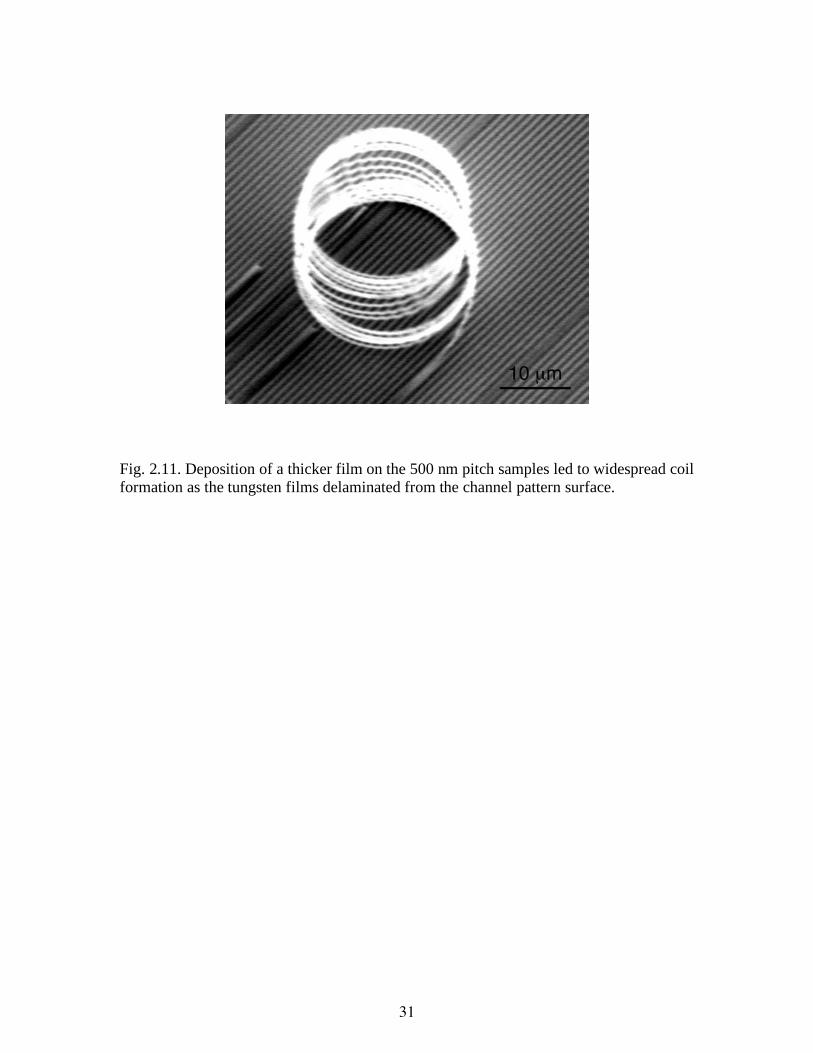
2.3.2 Results and Discussion The first attempt at deposition on the 500 nm pitch channel wafers resulted in incomplete film formation as shown in Fig. 2.9. This figure also shows that deposition was unidirectional, similar to evaporation, due to low processing pressures required for high compressive residual stresses. Nevertheless, the cross sections showed that the sputter deposited films completely filled the base of the channels and into the channel corners. The films on the channel pattern surface were uniform in thickness and readily delaminated as shown in Fig. 2.10. When these films delaminated they formed cracks that propagated along the channel pattern surface accompanied by through-thickness fracture of the tungsten films perpendicular to the channel walls. The intrinsic compressive residual stresses led to film roll, much like an edge lift off test. The films in the channels remained fully adhered. Deposition of a thicker film led to similar results, where delamination also occurred readily along the channel pattern surface. As shown in Fig. 2.11, the thicker film led to widespread coil formation across the sample surface as the tungsten films delaminated from the channel pattern surface. Again, the films in the channels remained fully adhered. Deposition of tungsten onto the 200 nm pitch sample created nearly uniform films across the surface. The films spontaneously delaminated following deposition forming two types of buckles. Small telephone-cord like buckles formed on the channel patterns by alternating segments running parallel and segments running perpendicular to the channels creating a telephone cord buckle running at a 45˚ angle to the channel pattern (Fig. 2.12a). Large straight-sided buckles formed perpendicular to the channel patterns. The buckle widths in both cases spanned many channels (Fig. 2.12b). Interfacial fracture energies were first determined from the telephone cord blisters shown in Fig. 2.12a and then compared to the fracture energy for tungsten on smooth silicon. Each set of data included six blisters. These results are summarized in Table 2.2. The data in Table 2.2 shows that the fracture energy increased from 0.6 to 0.9 J/m2 with the channel roughening. Nearly identical film thickness and deposition processes and high modulus and yield strength for the tungsten film negate the probability of plasticity being responsible for this increase. Using the same analysis for the large blisters running perpendicular to the channel patterns, Fig. 2.12(b), gives an average fracture energy of 0.85 J/m2. The values are slightly lower than those for blisters parallel to the channel patterns and accounts for their larger size. Nevertheless, unidirectional patterning increased the energy required for crack growth over that for a smooth interface.40
2.4 Roughened Surface Effects on Adhesion The purpose of this stage of the study was to develop an understanding of how random nanoscale heterogeneities affect interfacial fracture energy. This was accomplished by using sputter deposited tungsten films on lapped silicon substrates to determine how sub micron scale heterogeneities affect film fracture and by using hillock roughening of

18
silicon substrates to determine how nanoscale heterogeneities affect multilayer film sample fracture. 2.4.1 Lapped silicon substrates 2.4.1.1 Materials and Procedure Samples in this stage of the study were fabricated using the as-received side of the silicon wafers. The RMS surface roughness was 912 nm compared with the RMS roughness of 2 nm for the smooth polished surface silicon substrates, Fig. 2.13. A 200 nm thick film of tungsten was deposited onto the substrates at low working pressures to generate high compressive stresses. The difference in film thickness to surface roughness duplicates effects seen in a number of microelectronic applications. 2.4.1.2 Results There was no spontaneous delamination of the films from the rough substrates. This indicated that the energy required for delamination was much larger than for the as-polished smooth substrates described earlier. To qualitatively assess susceptibility to fracture, smooth and rough interface samples were subjected to nanoscratch testing. The scratch tests were conducted in load control while monitoring lateral force until a maximum load of 100 mN was attained. Fig. 2.14 shows the normal load and lateral response of the smooth sample and Fig. 2.15 shows the normal load and lateral response of the rough sample. The transition from a constant to an undulating friction coefficient indicates that the smooth film started to delaminate when scratch was 50 mN. Optical images of the surface showed blisters forming on either side of the scratches. The same loading is not seen with the scratch testing of the rough sample. Both the normal and lateral load is shown to undulate constantly during the scratch. The spikes indicate when the tip has come into and out of direct contact with Si substrate. Optical images of this sample revealed no blisters.40 Results showed that delamination was easily induced when the surface roughness is low (2nm). Although no clear conclusion can be made to show that the interfacial fracture energy actually increases with surface roughness, it is evident that the surface roughness controls the ability to apply uniform stresses to a localized area required for the delamination for systems where the film thickness is much less than the substrate roughness. 2.4.2 Hillock Roughening In fracturing samples with strong bonds, such as titanium, chromium, and tantalum nitride, significant effort has been devoted to test method development and sample preparation. The previously discussed fracture methods cannot always be used to

19
delaminate the desired interfaces. Stressed overlayer tests are often insufficient since the residual stress magnitudes in the films required for delamination and fracture are beyond those possible by current fabrication methods. Nanoindentation and nanoscratch techniques also cannot always be implemented since the far field stresses required for fracture can not always be generated in selected film systems. A relatively new method is four point bending. Using specific sample geometry and loading configurations, the four-point bending test technique measures the critical load sufficient for crack growth along an interface that can then be used to calculate the sample’s strain energy release rate required for crack growth. At this critical load where crack growth occurs, the strain energy release rate equals the interfacial fracture energy. This experimental technique was derived by originally Charalambides for laminate composites20, 21 and then further developed to measure the adhesion of thin films for microelectronics by Dauskardt et al.22-38. The bond strength of platinum films on silicon with titanium adhesion layers was measured as a function of hillock roughening. 2.4.2.1 Materials and Procedure Two systems were tested: platinum-on-titanium on 4 nm RMS and 15 nm RMS silicon substrates. The silicon substrates were fabricated using deep reactive ion etching (DRIE) of silicon wafers with SF6 and O2 gases. SF6, the etchant, ionizes into SF5, which reacts with the Si surface yielding the volatile product SiF4. O2 is used to generate more F- ions (increases etch rate), etch away the hydrocarbon residues, and form the passivating film SiXOXFX. To alter the Si surface, the gas flow rates, ICP power, RF power, time, pressure and temperature of the DRIE process were carefully selected. By increasing O2, passivation/etching cycle ratio (4/2), and operating at cryogenic temperature, -110°C, the ion exposure to the surface passivation film is limited, decreasing the etch rate and the degree of anisotropy causing ‘Black Silicon’ or ‘Silicon Grass’ formation, Fig. 2.16.40 In this application, grass roughening on the order of 20-30 nm was achieved. The silicon grass is removed leaving a roughened substrate, Fig. 2.17. A 175nm Pt film (with 6nm Ti) was deposited onto two wafers by DC magnetron sputtering. The processing pressure used was 11 mTorr with a forward power of 60 W. Scanning electron and atomic force microscopy, SEM and AFM, were used to characterize the silicon surface roughness, assess sputtering coverage, and evaluate interfacial fractures. Samples were then split along pre-scored lines and epoxy bonded together creating four point bend interfacial fracture samples.40 2.4.2.2 Results and Discussion Four point bend tests were used to measure resistance to interfacial fracture of the roughened interface samples. Fig. 2.18a shows a schematic of the four-point bend sample with loads and moments during test. Figure 2.18b shows the four-point bend fixture with sample in place. Of the three four-point bend samples made from each substrate and tested, only two exhibited crack initiation and propagation along an interface. In both cases, fracture occurred along the platinum-epoxy bonds at critical loads of 10.4 and 8.4

20
N. The critical loads of 10.4 and 8.4 N yield fracture energies of 18.21 and 11.88 J/m2 obtained using the following equation,
!
G =
21P2L2 1" #2$ % & '
( )
16Eb2h3 (2.7)
In this equation, G is the interfacial fracture energy, P is the load, E is the Young’s modulus, ν is Poisson’s ratio, L is the length between inner and outer load pins, b is the sample width and h is the sample height. While fracture along the platinum-epoxy bond is not the desired result, the results still yield useful information about the platinum-silicon interface strength. Since the fracture occurred between the epoxy and the thin metal film, it can be concluded that the platinum-epoxy interface has a lower interfacial fracture energy than does the silicon-platinum interface. Since the sample population of ‘no roughness wafers’ yielded an average adhesive toughness of 6.02 J/m2 to the roughened 15.04 J/m2, it can be concluded that adhesion strength does increase with increased surface roughness. 2.4.3 Continuing Work These initial tests showed that the fracture energy can be increased for an interface with uniform chemistry by altering the nanoscale patterning. However, the limited number of successful tests did not allow for conclusive results. Blister tests will be done in the future using these hillock Si samples using tungsten overlayers. If higher residual stresses are needed, nitride overlayers will also be used to drive delaminations.
2.5 Summary The experimental portion of this study focused on the effects of tailored interfacial chemistry on adhesion, use of unidirectional nanopatterns on fracture resistance and the effects of uniform nanoscale roughness on fracture. Using three different fracture techniques, nanoindentation, overlayers and four point bending, this study was able to show two significant findings. First, the interfacial energy scales with the area fracture coverage of the interface chemistry having the highest adhesion energy. Secondly, the unidirectional and hillock patterning both increase the energy required for crack growth over that for a smooth interface.

21
2.6 References 1. K. L. Mittal, Adhesion measurements of thin films, Electrocomponent Science
and Technology , 1976, 3, 21-42. 2. A. A. Volinsky, N. R. Moody, W. W. Gerberich, Interfacial toughness
measurements for thin films on substrates. Acta Mater., 2002, 50, 441-466. 3. R. Maboudian, R. T. Howe, Critical review: adhesion in surface micromechanical
structures, J. Vac. Sci. Technol. B, 1997, 15, 1-20. 4. M. D. Kriese, N. R. Moody, W. W. Gerberich, Effects of annealing and
interlayers on the adhesion energy of copper thin films to SiO2/Si Substrates, Acta
Mater., 1998a, 46, 6623-6630. 5. A. G. Evans, M. Ruhle, Microstructure and fracture resistance of metal/ceramic
interfaces, MRS Bulletin, 1990, XV, 1990, 46-50. 6. K. P. Trumble, M. Ruhle, The oxygen activity dependence of spinel interphase
formation during Ni/Al2O3 diffusion bonding, in “Metal-Ceramic Interfaces,” eds. M. Ruhle, A. G. Evans, M. F. Ashby, J. P. Hirth, Pergammon Press, Oxford, 1990, pp. 144-151.
7. A. G. Evans, J. W. Hutchinson, Overview on thermomechanical integrity of thin films and multilayers, Acta Metall. Mater., 1995, 43, 2507-30.
8. A. G. Evans, J. W. Hutchinson, Y. Wei, Interface adhesion: effects of plasticity and segregation, Acta Mater., 1999, 47, 4093-4113.
9. R. M. Cannon, B. J. Dalgleish, R. K. Dauskardt, T. S. Oh, R. O. Ritchie, Cyclic fatigue-crack propagation along ceramic/metal interfaces, Acta Metall. Mater., 39, 1991, 2145-2156.
10. A. G Evans, B. J. Dalgleish, The fracture resistance of metal-ceramic interfaces, Acta Metall. Mater., 1992, 40, S295-S306.
11. N. R. Moody, D. P. Adams, A. A. Volinsky, M. D. Kriese, W. W. Gerberich, Annealing effects on interfacial fracture in gold-chromium films in hybrid microcircuits, in "Interfacial Engineering for Optimized Properties II," eds. C. Briant, C. Carter, E. Hall, E., S. Nutt, Materials Research Society, Pittsburgh, PA 2000, vol. 586, 195-205.
12. N. R. Moody, D. P. Adams, D. Medlin, A. A. Volinsky, N. Yang, and W. W. Gerberich, Effects of Diffusion on the Interfacial Fracture of Gold-Chromium Microcircuit Films, Int. J. Fract., 2003, to be published.
13. S.W. Russell, S.A. Rafalski, R.L. Spreitzer, J. Li, M. Moinpour, F. Moghadam, T.L. Alford, Enhanced adhesion of copper to dielectrics via titanium and chromium additions and sacrificial reactions, Thin Solid Films, 1995, 262, 154-167.
14. M. Lane, R. H. Dauskardt, N. Krishna, I. Hashi, Adhesion and reliability of copper interconnects with Ta and TaN barriers, J. Mater. Res., 2000, 15, 203-211.
15. A. Furuya, N. Hosoi, Y. Ohishita, Evaluation of Cu adhesive energy on barrier metals by means of contact-angle measurement, J. Appl. Phys., 1995, 78, 5989-5992.
16. W. W. Gerberich, A. A. Volinsky , N. I. Tymiak, and N. R. Moody, in Thin
Films-Stresses and Mechanical Properties VIII, R. Vinci, O. Kraft, N. Moody, P.

22
Besser, and E. Schaffer II, eds. , Materials Research Society, Pittsburgh, PA, vol 594, pp. 351-364, 2000.
17. N. R. Moody, D. P. Adams, A. Mudd, M. J. Cordill, D. F. Bahr, Film Thickness Effects on Deformation and Fracture of Ultra-Thin Gold Film Adhesion, Proceedings ICM-9, S. R. Bodner, D. Rittel, D. Sherman, eds., (2003) CD-ROM Paper 145; SAND2003-8146, Sandia National Laboratories, Livermore, CA 94550.
18. S. K. Roy Chowdhury, H. M. Pollock, Adhesion between metal surfaces:The effect of surface roughness, Wear, 66 (1981) 307 - 321
19. D. R. Clarke, W. Pompf, Critical radius for interface separation of a compressively stressed film from a rough surface, Acta mater. 47, pp. 1749-1756, 1999
20. A. G. Evans, J. W. Hutchinson, Effects of non-planarity on the mixed mode fracture resistance of bimaterial interfaces, Acta metall., 37, No. 3, pp. 909-916, 1989
21. T. S. Oh, J. Rodel, R. M. Cannon, R. O. Ritchie, Ceramic/metal interfacial crack growth: toughening by controlled microcracks and interfacial geometries, Acta
Metall., 1988, 36, 2083-2093. 22. S. Zhang, R. Panat, K. J. Hsia, Influence of surface morphology on the adhesion
strength of epoxy –aluminum interfaces, J. Adhesion Sci. Technol., Vol. 17, No. 12, pp. 1685–1711 (2003)
23. A. F. Harris, A. Beevers, The effects of grit-blasting on surface properties for adhesion, International Journal of Adhesion & Adhesives 19 (1999) 445-452
24. T. Wakui, J. Malzbrender, R. W. Steinbrech, Mechanical testing of thermally stressed materials with rough interfaces: Mechanically induced delamination cracking in thermal barrier composites, Surface & Coatings Technology 200 (2006) 5419 – 5426
25. C. S. Litteken, R. H. Dauskardt, Adhesion of polymer thin-films and patterned lines, International Journal of Fracture 119/120: 475–485, 2003.
26. A. A. Volinsky, D. F. Bahr, M. Kriese, N. R. Moody, W. W. Gerberich, Nanoindentation Methods For Interfacial Fracture Testing, in Encyclopedia on Comprehensive Structural Integrity, vol. 8, Interfacial and Nanoscale Failure, W. W. Gerberich, W. Yang, vol. eds., I. Milne, R. O. Ritchie, B. Karihaloo, editors-in-chief, Elsevier, 2003, pp.453-493; SAND2002-8616. Sandia National Laboratories, Livermore, CA, 94550.
27. T. W. Wu, Microscratch and load relaxation tests for ultra-thin films, J. Mater.
Res., 1991, 6, 407-425. 28. P. Burnett, D. Rickersby, The relationship between hardness and scratch
adhesion, Thin Solid Films, 1987, 154, 403-416. 29. S. K. Venkataraman, D. L. Kohstedt, W. W. Gerberich, Microscratch analysis of
the work of adhesion for Pt thin films on NiO, J. Mater. Res., 1992, 7, 1126-1132. 30. S. K. Venkataraman , J. C. Nelson, A. J. Hsieh, D. L. Kohlstedt, W. W.
Gerberich, Continuous microscratch measurements of thin film adhesion strengths, J. Adhes. Sci. Technol., 1993a, 7, 1279-1292.
31. R. H. Dauskardt, M. Lane, Q. Ma, N. Krishna, Adhesion and debonding of multi-layer thin ®lm structures Engineering Fracture Mechanics 61 (1998) 141-162
32. A. Lee, C. S. litteken, R. H. Dauskardt, W. D. Nix, Comparison of the telephone

23
cord delamination method for measuring interfacial adhesion with the four-point bending method, Acta Materialia 53 (2005) 609–616. 33. D. B. Marshall, A. G. Evans, Measurement of adherence of residually stressed
thin films by indentation. I. mechanics of interface delamination, J. Appl. Phys. 1984, 56, 2632-2638.
34. M. D. Kriese, W. W. Gerberich, N. R. Moody, Indentation of superlayers as a quantitative probe of thin-film interfacial adhesion energy-I. mechanics of interfacial delamination, Journal of Materials Research, 1999, 14, 3007-3018.
35. A. Bagchi, G. E. Lucas, Z. Suo, A. G. Evans, A new procedure for measuring the decohesion energy for thin ductile films on substrates, J. Mater. Res., 1994, 9, 1734-1741.
36. A. Bagchi, A. G. Evans, Measurements of the debond energy for thin metallization lines on dielectrics, Thin Solid Films, 1996, 286, 203-212.
37. M. J. Cordill, D. F. Bahr, N. R. Moody, W. W. Gerberich , Recent Developments in Thin Film Adhesion Measurement, IEEE Transactions on Device and Materials Reliability, 4 (2) (2004) 163-168.
38. M.J. Cordill, D.F. Bahr, N.R. Moody, W.W. Gerberich, Adhesion Measurements Using Telephone Cord Buckles, Materials Science and Engineering A, 443 (2007) 150-155.
39. M.S. Kennedy, N.R. Moody, D.F. Bahr. The Effect of Non-Uniform Chemistry on Interfacial Fracture Toughness, Metallurgical and Materials Transactions A (2007) accepted for publication.
40. M. S. Kennedy, Ph.D. Thesis, Washington State University, Pullman, WA, 99164, 2007.
41. M. P. Hughey, D. J. Morris, R. F. Cook, S. P. Bozeman, B. L. Kelly, A. L. N. Chakravarty, D. P. Harkens, L. C. Sterns, Four-point bend adhesion measurements of copper and permalloy systems, Engineering Fracture Mechanics, 2004, vol. 71, pp. 245-261.
42. Colin J, Cleymand F, Coupeau C, Grilhe J. Worm-like delamination patterns of thin stainless steel films on polycarbonate substrates, Philosophical Magazine A: Physics of Condensed Matter, Structure, Defects and Mechanical Properties 2000, 80, 2559.
43. M.W. Moon, H.M. Jensen, J.W. Hutchinson, K.H. Oh, A.G. Evans, The characterization of telephone cord buckling of compressed thin films on substrates, J. Mech. Phys. Solids, 50 (2002) 2355-2377.
44. M. J. Cordill, N. R. Moody, D. F. Bahr, "Quantifying Improvements in Adhesion of Platinum Films on Brittle Substrates", Journal of Materials Research, 19 (2004) 1818-1825.
45. J. W. Hutchinson, Z. Suo, Mixed mode cracking in layered materials, in “Advances in Applied Mechanics,” eds. J. W. Hutchinson, T. Y. Wu, Academic Press Inc., New York, 1992, vol. 29, pp. 63-191.
46. N. R. Moody, R. Q. Hwang, S. Venkataraman, J. E. Angelo, W. W. Gerberich, Adhesion and fracture of tantalum nitride thin films, Acta Mater., 1998, 46 585-597.
47. N. R. Moody, N. Yang, D. P. Adams, M. J. Cordill, D. F. Bahr, The Effects of Copper on the Interfacial Fracture of Gold Films, in Thin Films: Stresses and Mechanical Properties IX, C. S. Ozkan, L. B. Freund, R. C.

24
Camarata, and H. Gao, eds. (Mater. Res. Soc. Proc., 695, Pittsburgh, PA, 2002) p. L7.5.1-L7.5.6
48. A. G. Evans, M. Ruhle, B. J. Dalgleish, and P. G. Charalambides, in Metal-Ceramic Interfaces. p. 345, Pergammon Press, Oxford (1990).
49. D. W. Hoffman, J. A. Thornton, The compressive stress transition in Al, V, Zr, Nb, aqnd W metal films sputtered at low working pressures, Thin Solid Films, 45, 1977, 387-396.
50. R. C. Sun, T. C. Tisone, P. D. Cruzan, The origin of internal stress in low-voltage sputtered tungsten films, J. Appl. Physics, 46, 1975, 112-117.
51. J. L. Devore, Probability and Statistics for Engineering Sciences, Cole, US: Brooks, 2002.
52. J. A. Emerson, T. R. Guess, C. Adkins, J. G. Curro, E. D. Reedy, Jr., E. P. Lopez, and P. Lemke, Investigation of the impact of cleaning on the adhesive bond and the process implications, SAND2000-1042, Sandia National Laboratories, Albuquerque, NM, (2000).
53. A. A. Talin, L. L. Hunter, F. Leonard, B. Rokad, Large area, dense silicon nanowire array chemical sensors, Applied Physics Letters, 89, 2006, 1-3.
54. M. D. Thouless, J. W. Hutchinson, E. G. Liniger, Plane-strain, buckling driven delamination of thin films: model experiments and mode-II fracture, Acta Metall.
Mater., 1992, 40, 2639-2649. Table 2.1 Fracture energies for sputter deposited tungsten on smooth and polymer patterned oxidized silicon wafers Film hW b δ σb σr Γ(ψ) ψ ΓΙ (nm) (µm) (µm) (GPa) (GPa) (J/m2) (J/m2) Smooth 250 14 1.4 0.1 -3.0 2.7 -90 0.6 Patterned 400 43 3.1 0.03 -1.5 1.0 -90 0.4 Table 2.2 Fracture energies for sputter deposited tungsten on smooth and channel patterned oxidized silicon wafers Film hW b δ σb σr Γ(ψ) ψ ΓΙ (nm) (µm) (µm) (GPa) (GPa) (J/m2) (J/m2) Smooth 250 14 1.4 0.1 -3.0 2.7 -90 0.6 Patterned small 280 13 1.4 0.2 -3.6 4.3 -90 0.9 large 280 85 1.1 0.004 -3.6 4.1 -90 0.8

25
(a)
(b)
(c) Fig. 2.1. (a) This image shows the uniform deposition of the polymer tubes. (b) Closer examination shows very uniform tubes were deposited with a diameter of 200 nm. (c) A tilted sectional view shows that the tubes stand approximately 500 nm high.

26
Fig. 2.2. The telephone cord buckles formed spontaneously when the 250nm compressive W film delaminated from the oxidized silicon substrate.
Fig. 2.3. AFM images were taken of the buckles that formed during the separation of the tungsten-oxidized silicon interface and this is a typical cross section. The interfacial energy of this interface was determined to be 0.6 J/m2.

27
Fig. 2.4a. Straight walled buckles formed spontaneously on the polymer patterned samples with some short telephone cord buckle formation.
Fig. 2.4b. Cross section of the buckle morphology seen in delamination along tungsten-oxidized silicon interface masked by polymer tubes.

28
Fig. 2.5. This image of the under side of the W film after delamination shows the pores made during deposition and the polymer tubes within these pores.
Fig. 2.6. A cross section schematic showing dimensions of a uniform width straight wall and telephone cord buckle.

29
Fig. 2.7. Nanoimprint lithography was used to create two dimensional rectangular-toothed patterns (i.e., parallel channels with a rectangular cross-section) in silicon wafer substrates as shown here for the 200 nm pitch sample.
Fig. 2.8. Reentrant corners at the base of the 500 nm pitch sample channels exhibited significantly more rounding than the 100 nm pitch sample channel corners.

30
Fig. 2.9. Sputter deposition onto the 500 nm pitch channel samples was unidirectional with partial channel fill. The films completely filled the base of the channels and channel corners.
Fig. 2.10. Films on the 500 nm pitch channel pattern surface were uniform in thickness and delaminated following deposition. Residual stresses led to film roll.
31
Fig. 2.11. Deposition of a thicker film on the 500 nm pitch samples led to widespread coil formation as the tungsten films delaminated from the channel pattern surface.

32
(a)
(b) Fig. 2.12. The films spontaneously delaminated following deposition forming two types of buckles. (a) Small telephone-cord like buckles formed on the channel patterns by alternating segments running parallel and perpendicular to the channels. (b) Large straight-sided buckles formed perpendicular to the channel patterns.

33
(a)
(b) Fig. 2.13. Optical micrographs showing silicon substrates with (a) 912 nm rms and (b) 2 nm rms surface roughness. The inserts are AFM deflection images of the substrate surfaces.

34
Fig. 2.14. Scratch test of tungsten on smooth silicon shows a distinct transition when film fracture occurs.
Fig. 2.15. The rough morphology prevents uniform loading of external stresses into the film system as shown by this plot of lateral and normal loading into the tungsten film on rough silicon.

35
Fig. 2.16. The silicon substrates were fabricated using deep reactive ion etching leading to silicon grass formation.40
Fig. 2.17. Removing the silicon grass leaves a roughened surface.

36
(a)
(b) Fig. 2.18. (a) Schematic of a multilayer film sample showing loads and moments in flexure during (b) four-point bend testing.

37
3. Finite Element Analysis of Cracking
Along a Patterned Interface
3.1 Introduction It is well known that interfacial roughness can increase interfacial toughness.1-5 This increase in toughness is thought to arise from a number of sources including an increase in the real interfacial surface area, enhanced plastic energy dissipation in the bulk materials, and mechanical interlock. The focus of the present work is to determine how geometric and material parameter choices affect the apparent toughness of thin film interfaces that have patterned nanoscale roughness. Here we limit the investigation to interfaces between elastic materials precluding the possibility of dissipation by plastic deformation in the bulk. In this case one would expect that an increase in apparent interfacial toughness is linked to the increased real surface area of an interface with patterned roughness. The apparent interfacial toughness could be further enhanced if strain energy is locked into the structure by contact, as might be the case under a mixed-mode (combined tensile and shear) loading. It is also possible that discontinuous crack growth could dissipate additional energy as kinetic energy that is then converted to thermal energy.
3.2 Finite Element Simulations The finite element simulations were performed using Sandia National Laboratories’ transient dynamics Presto 3-D finite element code.6 Presto 3-D uses explicit (time-stepping) integration techniques to resolve stress waves within a body. This type of code is particularly well suited to analyze problems with discontinuous events like those that might occur in complex, crack growth simulations. The loading rate was typically 1 nm/ns so as to ensure that the kinetic energy associated with the loading is negligible. Furthermore, two percent stiffness proportional viscous damping was used in all calculations to damp out high frequency stresses. A cohesive zone model, which is implemented in Presto 3-D via its contact algorithm, was used to simulate interfacial crack growth. In a cohesive zone model, interfacial separation is defined in terms of an effective interfacial traction vs. separation relationship (Fig. 3.1). Key parameters are the interfacial strength
!
ˆ " and the intrinsic work of separation/unit area Γo. A cohesive zone separation model is computationally attractive since crack growth is a natural outcome of the solution, and moreover it leads to mesh-independent results since a length scale is embedded within the model (provided that the mesh is fine enough to resolve the cohesive zone at the crack tip). The particular cohesive zone formulation used in this study is similar to that used by Tvergaard and Hutchinson.7 The contact algorithm does provide constraint against normal interpenetration. The effective separation λ is defined as

38
!
" =#n
#n
c
$
% &
'
( )
2
+#t
#t
c
$
% &
'
( )
2
(3.1)
where δn and δt are the normal and tangential displacement jump across the interface while
!
"n
c and
!
"t
c are the respective critical values. Since there is no compelling reason to assume otherwise,
!
"n
c= "
t
c= " c is assumed. The normal and tangential interfacial tractions
(Tn and Tt, respectively) are defined via the potential
!
"(#n,#
t) = # c $( % & )
0
&
' d % & (3.2)
with
!
Tn
="#
"$n
=%(&)
&
$n
$ cand T
t="#
"$t
=%(&)
&
$t
$ c . (3.3)
The shape of the traction-separation relation has been found to be relatively unimportant7. Consequently, for the sake of simplicity a simple triangular relationship with a steep loading segment was used (typically used λ1=0.02). The work of separation per unit area of interface is path independent and equals the value of the potential φ evaluated at λ = 1 (eq. 3.2). For the assumed triangular relationship, the intrinsic work of separation Γo equals
!
ˆ " #c
2. In this study the separation relationship represents in, a rudimentary way, the atomistic separation process. In most calculations, an intrinsic work of separation of 0.3 J/m2 is used; a value consistent with that measured value for a SiO2/W interface.8 The critical separation distance δc is taken to be one nm. Fig. 3.2 shows the idealized, thin film bimaterial strip geometry analyzed. This particular plane strain geometry was chosen for its simplicity and because the solution for a flat interface is known and consequently provides a baseline to compare against. Furthermore, its thinness allows for relatively rapid stress equilibration during loading. The strip is composed of two layers, each with thickness h. The top layer will be referred to as the film, while the bottom layer will be called the substrate. An 80a length of the patterned interface is initially unbonded (Fig. 3.2). The strip is subjected to a fixed grip loading where the top edge is displaced relative to the fixed lower edge. Consequently any desired global mixed-mode loading can be easily applied by varying the ratio of normal to tangential edge displacement. Most calculations were performed for a rectangular-toothed pattern (Fig. 3.2b), although some calculations were also performed for a rippled interface (Fig. 3.2c). The patterns are defined by the characteristic lengths a and b. Note that these 2-D, plane strain models actually define parallel channels with either a rectangular-toothed or rippled cross-section. The side length of elements along the interface was typically 5 nm. Unless indicated otherwise, reported results are for a bimaterial composed of tungsten film (E=410 GPa, ν=0.28) on a silicon substrate (E=161 GPa, ν=0.23). The efficacy of a given interfacial pattern is quantified in terms of its apparent toughness, Γa. Apparent toughness is defined as the toughness that a similar bimaterial strip, but with a flat interface, would have to have for crack growth to initiate at the same load level. Load level can be defined in terms of the normal
!
"n
* and shear stress,
!
" * found in the uniformly stressed region far ahead of the crack tip. Based upon energy

39
considerations, it is easy to show that for a bimaterial strip with a total thickness of 2h (Fig. 3.2)
!
"a
=#n
*2
h
Eu
+$*2h
G (3.4)
where the equivalent uniaxial strain modulus Eu is given by
!
Eu
= 2 1/Eu1
+1/Eu2( )
"1 with
!
Eui
= 2Gi(1"#
i) (1" 2#
i) (3.5)
and where the equivalent shear modulus G is given by
!
G = 2 1/G1
+1/G2( )"1
(3.6)
Here Ei is the Young’s modulus, νi is the Poisson’s ratio and Gi is the shear modulus of layer i=1 (film) or 2 (substrate). Table 3.1 lists results of test calculations that illustrate the accuracy of the modeling techniques used. The tungsten/silicon bimaterial analyzed has an intrinsic interfacial toughness Γo=0.3 J/m2 and a film thickness h=250 nm. For the case of a flat interface, the apparent toughness should equal the intrinsic toughness. Furthermore, the results should be independent of the interfacial strength
!
ˆ " as long as the element size is small enough to resolve the cohesive zone and the cohesive zone length is small relative to other geometric length scales. Table 3.I shows that the calculated results are consistent with expectation and that a mesh with 5 nm long interfacial elements is sufficient to resolve the cohesive zone. Table 3.1 also lists results for a rectangular channel interface pattern with a=b=25 nm. Calculations were performed for both the standard mesh and a refined mesh with 2.5-nm long interfacial elements. First notice that the calculated results do depend on the choice of interfacial strength (the reason for this will be discussed in detail below). For a given value of interfacial strength, the Γa values determined using the refined mesh are in acceptable agreement with those determined using the standard mesh (within 7% when
!
ˆ " =600 MPa and within 4% when
!
ˆ " =1000 MPa). Given the complex failure process, calculated results are adequate for comparing the apparent toughness of bimaterial strips with one interfacial pattern to another. Also note that Γa scales with the square of the load.
3.3 Results Calculations have been performed for a wide range of material and geometric parameters. Unless indicated otherwise, all results are for a tungsten/silicon bimaterial strip that 1) has a square channel interface pattern with a=b=25 nm, 2) is subjected to a global mode I loading, 3) has h=250 nm, and 4) has an interface with Γo=0.3 J/m2 and
!
ˆ " =600 MPa. First consider the effect of interfacial strength
!
ˆ " on calculated apparent toughness Γa (δc is adjusted to maintain Γo=0.3 J/m2). Figs. 3.3 through 3.8 plot the calculated traction vs. edge displacement for the three positions adjacent to the initial crack tip: position A is at the tip of the silicon tooth, position B is at the middle of the channel wall, and position C is at the tip of the tungsten tooth (see the insert in the Figures). When
!
ˆ " =300 MPa, the

40
crack does not grow (Fig. 3.3). Instead the entire uncracked ligament separates in a uniform manner as the interface follows the unloading path defined by the traction-separation relationship (Fig. 3.1). The far field ligament stress
!
"n
* reaches a maximum prior to separation. Consequently, the concept of an apparent interfacial toughness does not apply when the interface strength is relatively low. When
!
ˆ " is 400 MPa or higher, the crack does grow. Crack growth initiates first ahead of the main stalled crack along an interfacial segment at the tip of the tungsten tooth (point C) and then at the tip of the silicon tooth. Here initiation is defined as when softening behavior commences and the cohesive zone first begins to form. Ultimately, the sidewall fails (point B) and the stalled crack propagates rapidly. Note that segment cracking at tooth tips typically initiate throughout the ligament prior to rapid propagation although rapid cracking always initiates from the stalled crack tip where conditions are more critical. Also note that tooth-to-tooth stress transfer gives rise to a uniform ligament stress state once beyond the region immediately surrounding the patterned interface. The most important observation is that crack growth process is discontinuous with crack initiation in front of the stalled crack tip. The interface does not simply unzip in a continuous manner. The rapidity at which the tooth-tip interfacial segments (point A and C) fail is a strong function of interfacial strength. As
!
ˆ " increases from 400 MPa to 1200 MPa (Figs 3.4-3.7), the interfacial segment at the tip of the tungsten tooth fails more rapidly and unloads more fully prior to sidewall failure and rapid growth of the stalled crack. As noted in Table 3.2, the maximum applied load did not coincide with the rapid propagation of the stalled crack when
!
ˆ " =400 MPa and when
!
ˆ " =1200 MPa. When
!
ˆ " =1200 MPa, the interfacial segment at the tip of all the tungsten teeth had completely failed prior to rapid propagation of the stalled crack (i.e., voids at the tip of the tungsten teeth formed throughout the entire ligament). The calculation of an apparent toughness (eq. 3.4) is most appropriate when crack growth coincides with peak load (as is the case in linear elastic fracture mechanics). Nevertheless, the apparent toughness has been computed for such cases based on the
!
"n
* value corresponding to the rapid propagation of the stalled crack (Table 3.2). Results listed in Table 3.3 indicate that elastic properties of the substrate also have a strong influence on apparent toughness. All results are for a tungsten film while the substrate elastic properties range from tungsten to silicon to aluminum to graphite. The apparent toughness increases as the substrate becomes more compliant. Note that the quantity α listed in the Table 3.3 is one of Dundurs’ elastic mismatch parameters. It is defined as
!
" = (E 1# E
2) /(E
1+ E
2) (3.7)
where
!
E i= E
i/(1"#
i
2) for plane strain. Table 3.4 lists apparent toughness values for
three different values of intrinsic toughness (δc fixed at 1 nm). The apparent toughness increases with intrinsic toughness. Results in Tables 3.5 through 3.7 show how apparent toughness varies with geometric parameters. Results for a bimaterial strip with h=500 and for a=b, indicate that the apparent toughness increases with the characteristic length scale of the pattern (Table 3.5). Table 3.6 results indicate that apparent toughness increases as the aspect ratio of the
41
tooth, b/a, increases (a is fixed at 25 nm). A pattern with a longer tooth has a higher apparent toughness. The ratio of film thickness h to pattern characteristic length a can also affect apparent toughness (Table 3.7). These results suggest that film thickness must be 20 times the pattern height for apparent toughness to become insensitive to film thickness (compare results for a =12 nm for h=250 nm and 500 nm). Calculations were also performed for a range of global mode mixity (Table 3.8, Fig. 3.9). Global mode mixity is defined as tan-1(
!
" */
!
"n
* ). As one expects, apparent toughness increases with global mode mixity. Note that for a mode mixity of 36o or higher the calculated apparent toughness corresponds to the rapid propagation of “z”-cracks (see insert in Fig. 3.9, one of the sidewalls remains bonded). A few illustrative calculations were also performed for a rippled interface (Fig. 3.2c). Table 3.9 compares results for square channel and rippled channel patterns with the same characteristic lengths of a=b=25 nm. Note that when a=b, the true interfacial area of the rippled interface is 1.48 times that of a flat interface while the interfacial area of a square channel interface is twice that of a flat interface. The apparent toughness is greater for the interface with the higher true interfacial area.
3.4 Discussion The discontinuous nature of the calculated crack growth process is not surprising. The crack-tip is stalled as it tries to kink in a direction that is perpendicular to its original path. It is well known that the energy release rate, G, at the tip of a kinked crack can be significantly less than its value prior to kinking. For example, the energy release rate at the tip of kinked crack, where the kink angle is 90o from the initial crack plane, is only one fourth of the energy release rate that would exist if the crack had advanced straight ahead.9 In the problems analyzed, it was easier to initiate cracking on interfacial segments at the tip of the teeth in the rectangular-toothed channel pattern than to kink the original crack 90o. Presumably, local stress concentrations determine which tooth segments crack first (i.e., at the tip of the tungsten teeth rather than at the tip of the silicon teeth). One expects that apparent toughness should at least scale with true interfacial area for crack-like interfacial failure; when the transition to rapid crack propagation is abrupt and coincides with the calculated peak ligament stress. In other words,
!
"a/(A
r"o) >1 (3.8)
where Ar is the ratio of true to nominal interfacial area. The
!
"a/(A
r"o) values reported in
Tables 3.2-3.9 are broadly consistent with this expectation. There are some cases where this ratio falls below a value of one, but in those cases the transition to rapid crack propagation is less abrupt (e.g., compare Figs. 3.4 and 3.5). In fact, the energy dissipated should still equal at least ArΓo in those cases. Values of less than one are thought to be associated with the use of a linear elastic fracture mechanics calibration (eq. 3.4) that is not strictly applicable when crack propagation is less than abrupt.

42
Many of the reported
!
"a/(A
r"o) values are significantly greater than one. The reason
for this appears to be associated with the relative speed of the crack formation at the tip of the teeth in the rectangular-channel pattern once segment cracking initiates. Crack initiation is governed by interfacial strength
!
ˆ " . Under a locally mode-I like loading, a crack cannot initiate on the interfacial segment at the tip of a tooth until the interfacial normal stress exceeds
!
ˆ " . Once cracking can initiate, the rapidity with which it fails depends on the energy available to fail the tooth-tip interfacial segment. Here we use a simple estimate for the stress needed to crack a tooth-tip segment as a relative measure of the tendency for segment cracking. Using well known results,9 the energy release rate for an isolated crack of length 2l lying on the interface between two semi-infinite blocks subject to remote stress σ* can be shown to equal
!
G = ("# *2
l /E*) (3.9)
where
!
E*
= 2(1/E 1+1/E
2)"1with
!
E i defined previously (eq. 3.7) and where Dundurs’
parameter β is assumed to equal zero (a common approximation).9 The estimated segment cracking stress, σc, is simply taken to equal the stress required to fully open and advance an interfacial crack of length 2a along an interface with toughness Γo (here a is the characteristic pattern length as defined in Fig. 3.2b). Using eq. 3.9,
!
"c
=E*#0
$a (3.10)
Note that σc values are comparable only when the aspect ratio a/b is held fixed since eq. 3.10 does not consider the details of the pattern geometry. The ratio of
!
ˆ " /σc is the desired figure of merit. When this ratio is relatively high, the stress to initiate segment cracking is high compared to the stress needed to open the crack, and once initiated the crack will form relatively abruptly. The crack segment fails dynamically to create kinetic energy that is then dissipated by viscous damping in the calculation. When the value of
!
ˆ " /σc is relatively low, it is difficult to open the interfacial segment once cracking is initiated. The
!
ˆ " /σc values reported in Tables 3.2-3.7 clearly correlate with
!
"a/(A
r"o) values. Higher
values of
!
ˆ " /σc correspond to higher values of
!
"a/(A
r"o) . Fig. 3.10 plots the results listed
in Tables 3.2-3.5 that encompass variations in interfacial strength
!
ˆ " , substrate elasticity α, intrinsic toughness Γo, and characteristic length a (all for a=b nm). Fig. 3.10 shows that the
!
ˆ " /σc figure of merit rationalizes these variations in a simple way. Apparent interfacial toughness also increases with the applied global mode mixity (Fig. 3.9). This result is fully expected. Previous work has shown that interfacial roughness can contribute to increases in interfacial toughness with increasing load mode mixity10. Strain energy is locked into the films by persistent contact and cannot be released to create new surfaces. Finally note that Table 3.9 suggests that results for a rippled channel interface (Ar = 1.5) and a square-channel interface (Ar = 2.0) are quite similar when suitable scaled by the appropriate Ar value. As with the rectangular-toothed channel interface pattern, the crack growth process is discontinuous with crack initiation at the tip of the teeth prior to sidewall failure on the descending portion of the interface. This suggests that the actual shape of the pattern may be less important than one might suppose as long as the failure process is similar.

43
3.5 Conclusions
The most important finding is that the apparent interfacial toughness scales directly with real interfacial area. Consequently, apparent toughness can be increased by increasing the length-to-width aspect ratio of the pattern (increase b/a, Fig. 3.2). However, this ratio cannot be increased without limit. For example as the teeth in a rectangular-channel pattern become relatively long, increased tooth-to-tooth stress transfer will increase the stress at the root of the tooth and the tooth could fracture. This is one aspect of the problem that still needs to be considered. The apparent interfacial toughness also scales directly with a figure of merit that compares interfacial strength,
!
ˆ " , to a measure of the stress needed to open the interfacial segment once cracking initiates. This segment cracking stress, σc, varies as (E*Γo/a)1/2 were E* depends on the mismatch in film/substrate elastic properties, Γo is the intrinsic interfacial toughness, and a is the characteristic length scale of the pattern. Apparent toughness tends to increase with increasing
!
ˆ " /"c as segment failure becomes more abrupt and brittle-like. The increased
energy dissipation is associated with a more dynamic failure process with kinetic energy dissipated by viscous damping in the calculation. It is not clear if a more brittle-like failure is desirable or not. Furthermore, the increase in apparent toughness with increasing
!
ˆ " /"c is not without limit. At relatively high values of
!
ˆ " /"c, voids can
propagate throughout the entire ligament prior to rapid cracking (Fig. 3.8 where
!
ˆ " =1200 MPa). There are several other aspects of the problem that need to be considered. For instance the effect of residual film stress was not examined. The calculated results also reflect the cohesive zone model used. The model used in this study is based on a potential function and has no intrinsic dependence on mode mixity. The accuracy of this assumption is unknown. That question provided the motivation for the atomistic study of interfacial separation discussed in the next chapter.

44
3.6 References
1. J. A. Emerson, T. R. Guess, C. Adkins, J. G. Curro, E. D. Reedy, Jr., E. P. Lopez,
and P. Lemke: Investigation of the impact of cleaning on the adhesive bond and the process implications, SAND2000-1042, Sandia National Laboratories, Albuquerque, NM, (2000).
2. D. E. Packham: Surface energy, surface topography and adhesion. International
Journal of Adhesion and Adhesives 23, 437 (2003). 3. A. V. Pocius: Adhesion and adhesives technology. (Hanser Gardner Publications,
Inc.: Cincinnati, 1997). 4. A. N. Rider, and D. R. Arnott: The influence of adherend topography on the
fracture toughness of aluminum-epoxy adhesive joints in humid environments. Journal of Adhesion 75, 203 (2001).
5. S. Zhang, R. Panat, and K. J. Hsia: Influence of surface morphology on the adhesion strength of epoxy-aluminum interfaces. Journal of Adhesion Science and
Technology 17, 1685 (2003). 6. J. R. Koteras, and A. S. Gullerud: Presto user’s guide version 1.05. SAND2003-
1089, Sandia National Laboratories, Albuquerque, NM, (2003). 7. V. Tvergaard, and J. W. Hutchinson: The influence of plasticity on mixed mode
interface toughness. Journal of the Mechanics and Physics of Solids 41, 1119 (1993).
8. M. J. Cordill, D. F. Bahr, N. R. Moody, and W. W. Gerberich: Recent developments in thin film adhesion measurement. IEEE Transactions on Device
and Materials Reliability, 163 (2004). 9. J. W. Hutchinson, and Z. Suo, Mixed mode cracking in layered materials. In
Advances in applied mechanics, J. W. Hutchinson; T. Y. Wu, Eds. Academic Press: 1992; Vol. 29, pp 63.
10. A. G. Evans, and J. W. Hutchinson: Effects of non-planarity on the mixed mode fracture resistance of bimaterial interfaces. Acta Metallurgica 37, 909 (1989).

45
Table 3.1. Illustrative finite element results demonstrating the accuracy and convergence of calculated apparent toughness Γa (tungsten film, on a silicon substrate, h=250 nm, square channel interface pattern has a=b=25 nm, Γo=0.3 J/m2, global mode I loading).
Pattern
type Interfacial
element length (nm)
!
ˆ " (MPa)
!
"a
(J/m2)
flat 5.0 600 0.31 flat 5.0 1000 0.30
square 5.0 600 0.58 square 2.5 600 0.62 square 5.0 1000 1.47 square 2.5 1000 1.53
Table 3.2. Apparent toughness Γa as a function of interfacial strength
!
ˆ " (tungsten film on a silicon substrate, h=250 nm, square channel interface pattern with a=b=25 nm, Γo=0.3 J/m2, global mode I loading).
!
ˆ "
(MPa)
!
"c
(MPa)
!
ˆ " /"c
!
"a
(J/m2)
!
"a/(A
r"o)
400 970 0.41 0.421 0.70 600 970 0.62 0.58 0.97 800 970 0.83 0.78 1.30
1000 970 1.03 0.88 1.47 1200 970 1.24 0.901 1.50
1 Maximum applied load does not coincide with crack propagation. Table 3.3. Apparent toughness Γa as a function of substrate material (tungsten film, h=250 nm, square channel interface pattern with a=b=25 nm, Γo=0.3 J/m2,
!
ˆ " =600 MPa, global mode I loading).
E
(GPa)
ν α
!
"c
(MPa)
!
ˆ " /"c
!
"a
(J/m2)
!
"a/(A
r"o)
tungsten 410 0.28 0.00 1300 0.46 0.47 0.79 silicon 161 0.23 0.45 970 0.62 0.58 0.97 aluminum 69 0.32 0.71 710 0.85 0.68 1.13 graphite 17 0.30 0.92 370 1.62 0.891 1.48 1 Maximum applied load does not coincide with crack propagation.

46
Table 3.4. Apparent toughness Γa as a function of intrinsic interfacial toughness Γo (tungsten film on a silicon substrate, h=250 nm, square channel interface pattern with a=b=25 nm, global mode I loading).
!
"o
(J/m2)
!
ˆ "
(MPa)
!
"c
(MPa)
!
ˆ " /"c
!
"a
(J/m2)
!
"a/(A
r"o)
0.2 400 790 0.51 0.34 0.84 0.3 600 970 0.62 0.58 0.97 0.4 800 1120 0.71 0.90 1.13
Table 3.5. Apparent toughness Γa as a function of characteristic length a (tungsten film on a silicon substrate, h=500 nm, square channel interface pattern with a=b, Γo=0.3 J/m2,
!
ˆ " =600 MPa, global mode I loading).
a
(nm)
!
"c
(MPa)
!
ˆ " /"c
!
"a
(J/m2)
!
"a/(A
r"o)
12 1400 0.43 0.51 0.85 25 970 0.62 0.72 1.20 50 690 0.88 0.86 1.44
Table 3.6. Apparent toughness Γa as a function of channel pattern aspect ratio b/a (tungsten film on a silicon substrate, h=250 nm, pattern has a=25 nm, Γo=0.3 J/m2,
!
ˆ " =600 MPa, global mode I loading).
b/a Ar
!
"c
(MPa)
!
ˆ " /"c
!
"a
(J/m2)
!
"a/(A
r"o)
0.5 1.5 970 0.62 0.40 0.89 1.0 2.0 970 0.62 0.58 0.97 1.5 2.5 970 0.62 0.83 1.10

47
Table 3.7. Apparent toughness Γa as a function of film thickness h (tungsten film on a silicon substrate, pattern has a=b, Γo=0.3 J/m2,
!
ˆ " =600 MPa, global mode I loading).
h
(nm) a
(nm) h/a
!
"c
(MPa)
!
ˆ " /"c
!
"a
(J/m2)
!
"a/(A
r"o)
250 12 21 1400 0.43 0.48 0.81 250 25 10 970 0.62 0.58 0.97 250 50 5 690 0.88 0.491 0.81 500 12 42 1400 0.43 0.51 0.85 500 25 20 970 0.62 0.72 1.20 500 50 10 690 0.88 0.86 1.44
1 Maximum applied load does not coincide with crack propagation. Table 3.8. Apparent toughness Γa as a function of the global mode mixity (tungsten film on a silicon substrate, h=250 nm, square channel interface pattern with a=b=25 nm, Γo=0.3 J/m2,
!
ˆ " =600 MPa).
Global mode mixity (degrees)
!
"a
(J/m2)
!
"a/(A
r"o)
0 0.58 0.97 20 0.64 1.07 36 0.701 1.17 56 0.871 1.46 75 1.061 1.77
1 Defined by the formation of z-cracks (one side-wall still bonded).
Table 3.9. Apparent toughness Γa as a function of type of interfacial channel pattern (tungsten film on a silicon substrate, h=250 nm, pattern has a=b=25 nm, Γo=0.3 J/m2,
!
ˆ " =600 MPa, global mode I loading).
Pattern type
Global mode mixity
(degrees) !
ˆ " (MPa)
!
"c
(MPa)
!
ˆ " /"c
!
"a
(J/m2)
!
"a/(A
r"o)
ripple 0 600 970 0.62 0.44 0.99 square 0 600 970 0.62 0.58 0.97 ripple 0 1000 970 1.03 0.62 1.40 square 0 1000 970 1.03 0.88 1.47 ripple 19 600 970 0.62 0.49 1.11 square 20 600 970 0.62 0.64 1.07

48
Fig. 3.1. Traction-separation relationship used in finite element calculations.
Fig. 3.2. Geometry of film on a patterned substrate model analyzed (2a). Both rectangular and rippled channel interface patterns considered (2b and 2c).
b
a
b
a
2b 2c
uniformly displace top edge
2h
unbonded
pattern film
substrate
bottom edge fixed
2a
1

49
Fig. 3.3. Calculated interfacial traction as a function of applied edge loading when
!
ˆ " =300 MPa (tungsten film on a silicon substrate, h=250 nm, square channel interface pattern with a=b=25 nm, Γo=0.3 J/m2, global mode I loading).
A B C

50
Fig. 3.4. Calculated interfacial traction as a function of applied edge loading when
!
ˆ " =400 MPa (tungsten film on a silicon substrate, h=250 nm, square channel interface pattern with a=b=25 nm, Γo=0.3 J/m2, global mode I loading).
A B C
51
Fig. 3.5. Calculated interfacial traction as a function of applied edge loading when
!
ˆ " =600 MPa (tungsten film on a silicon substrate, h=250 nm, square channel interface pattern with a=b=25 nm, Γo=0.3 J/m2, global mode I loading).
A B C

52
Fig. 3.6. Calculated interfacial traction as a function of applied edge loading when
!
ˆ " =800 MPa (tungsten film on a silicon substrate, h=250 nm, square channel interface pattern with a=b=25 nm, Γo=0.3 J/m2, global mode I loading).
A B C

53
Fig. 3.7. Calculated interfacial traction as a function of applied edge loading when
!
ˆ " =1000 MPa (tungsten film on a silicon substrate, h=250 nm, square channel interface pattern with a=b=25 nm, Γo=0.3 J/m2, global mode I loading).
A B C

54
Fig. 3.8. Calculated interfacial traction as a function of applied edge loading when
!
ˆ " =1200 MPa (tungsten film on a silicon substrate, h=250 nm, square channel interface pattern with a=b=25 nm, Γo=0.3 J/m2, global mode I loading).
A B C

55
Fig. 3.9. The normalized apparent toughness as a function of the global mode mixity (see Table 3.8).
Γa/(Γ
oA
r)
Z=crack

56
Fig. 3.10. Normalized apparent toughness as a function of the ratio of interfacial strength-to-segment cracking stress (varied
!
", ˆ # , $o, and a in the calculations).
Vary
!
ˆ " (Table 3.2) Vary α (Table 3.3) Vary Γo (Table 3.4) Vary a (Table 3.5)
!
ˆ " /"c
Γa/(Γ
oA
r)
57
4. Molecular Dynamics Simulations of
Interfacial Separation
4.1 Introduction Modern approaches to the modeling and simulation of fracture are typically based on some type of cohesive methodology. That is, a constitutive model that exhibits a finite amount of cohesion, or work of separation, is used within a finite element (FE) framework. While some of these approaches use such a constitutive model for bulk elements (e.g. the Virtual Internal Bond method by Gao and Klein1,2), the more common approach is the use of cohesive surface elements (CSE), i.e. elements that possess zero volume in an undeformed state that are inserted between bulk elements. CSEs are particularly appropriate when the fracture path can be well-reasoned, such as to model interfacial delamination between multilayer structures. Such structures are common to micro-electronics systems where nanometer to micron thick layers of metals, ceramics and other materials are arranged according to specific designs. These layered materials are often subject to extremely large stresses either during their manufacturing or during device operation, and these stresses can lead to delamination of the various interfaces. Hence, predictive modeling and simulation of this process is beneficial towards a robust device design.
Constructing constitutive models used with CSEs has been a challenging exercise in mechanism-deduction and physical reasoning for the past decade and a half. The most notable initial works in this field are the articles by Tvergaard & Hutchinson3 and Xu & Needleman.4,5 In the first article, the authors define a traction-separation relation in terms of a traction potential. This potential depends on an effective separation that is a function of both the normal and tangential displacement jumps across the crack plane. The resulting expressions for normal and tangential tractions have similar forms, differing only by a multiplicative term proportional to the amount of normal or tangential displacement, respectively. The work of separation per unit area of interface is independent of the mode of loading. Xu and Needleman used a more complex form that defines normal response using the exponential form suggested by a fit to atomistic calculations. Although separate forms of work of separation are defined for normal and tangential loadings, the ultimate work to fail the interface is independent of the mode of loading when the normal separation becomes large compared to the model’s characteristic length scale.
More recent approaches to studying interfacial fracture have included the use of atomistic simulation for both the discovery of mechanisms active during the delamination process, and for motivating the functional form of constitutive relations used with CSEs. Gall et al. used such an approach to study tensile debonding of an aluminum-silicon interface.6 While considering only mode I type loading, they did manage to compare their simulation results with the model by Tvergaard and Needleman as well as earlier models

58
by Needleman,7,8 and develop impressive insight based on this comparison. Rottler et al. used molecular dynamics (MD) simulations to understand the physics governing crack formation and crazing in glass polymers.9,10 While their objective was neither to develop nor verify a CSE constitutive model, the resulting body of work does much to illuminate the characteristics needed by such a model for these types of materials. One approach that did attempt to use atomistic simulation results as a basis for the development of a cohesive relation is the one by Spearot et al.11 Their work focused on using MD to characterize a grain boundary interface model of copper as represented by the Embedded Atom Method by Foiles et al.12 Spearot et al. considered both normal and tangential displacement loading for their MD system, and developed a complex nonlinear elastic separation potential that included loading path-history dependent effects along with active and passive internal state variables (ISVs) to capture the mechanisms of dislocation creation, accumulated plasticity, and compositional intermixing. The development of a cohesive surface model for intergranular fracture in a face-centered-cubic (fcc) metal was also considered by Yamakov et al.13 They highlighted simulations that display both brittle (i.e. bond breaking) and ductile (in this case, the formation of twins from the crack tip) fracture mechanisms. The authors developed specific metrics to quantify crack opening displacement, and combined their estimates of crack opening displacement and normal stress to construct a qualitative model of traction-separation for both sets of mechanisms observed.
The articles by Spearot et al. and Yamakov et al. show impressive efforts to use atomistic simulation methods to feed into the development of CSE constitutive models. However, both efforts are aggressive in analyzing systems prone to plasticity and ductile fracture. The more straight-forward use of these methods for analyzing brittle fracture was not done. Furthermore, all of the articles cited above assume the existence of a single potential function that governs traction-separation behavior, even in cases where mixed-mode loading was considered. MD simulation has thus far not been used to verify if the existence of such a function has merit. In the present article, we use MD simulation to examine mixed-mode loading that leads to interfacial delamination. The propagation of a model crack along an interface between two brittle materials is simulated under various combinations of far field tensile (mode I) and shear (mode II) stresses. Local stress and local opening data under the steady-state crack propagation condition is extracted from these molecular dynamics simulations, and then used to determine analytical stress vs. opening relations for mixed mode loading conditions. The goal of our work is to develop a qualitative picture of the traction-separation behavior, similar to the approach by Yamakov et al., but also develop individual normal and shear traction-separation relations based on functional forms and parameters suggested by our simulation results.
4.2 Simulation Approach In this section, we present the methods and models used to perform our MD simulations. Specifically, we discuss the interatomic potentials developed to represent aspects of the behavior of body-centered-cubic (bcc) metals, a modification to these potentials that was

59
necessary to simplify the simulation of interfacial fracture, and details regarding our system size, crystal orientation, geometry and loading.
4.2.1 Interatomic potentials for bcc metals
Material fracture behavior is determined by material properties such as cohesive energy (Ec), surface energy (γ), and brittleness (ρ). The quantity of brittleness is defined by Rice
and Thomson14 as the ratio ρ = !
bG " , where G is shear modulus, b is magnitude of
Burgers vector, and γ is surface energy. Clearly, low values of ρ characterize ductile materials whereas high values characterize brittle materials. To understand the dependencies between fracture behavior and Ec, γ and ρ using molecular dynamics simulation approaches, a framework of generic interatomic potentials that do not necessarily pertain to specific materials yet allow systematic change of the predicted material properties is highly desired. This is because although these potentials may not directly relate the results to real materials, they are more instructive to construct a general cohesive zone law. Because we intend to study brittle materials and bcc crystals are more brittle than fcc crystals, we confine our study to bcc materials.
Simple pair potentials with short cutoff distances are used due to their high computational efficiency and ease of implementation. It is noted that in bcc crystals each atom has eight nearest neighbors and six next nearest neighbors whereas in fcc crystals each atom has 12 nearest neighbors and six next nearest neighbors. If the sum of the pairwise energy is dominated by the nearest neighbor bonding, it would appear at a first sight that fcc crystals would always have lower (more negative) cohesive energies (therefore more stable) than bcc crystals. In bcc crystals, however, the next nearest neighbor distance is only about 15% longer than the nearest neighbor distance (compared with 41% in fcc crystals). This suggests that bcc crystals can be viewed as approximately having 14 nearest neighbors. It is then possible to design a pair potential that favors bcc over fcc crystals by using appropriate shape and cutoff distance of the potential.
Both Morse and Lenard Jones potential formats were explored. Lenard Jones potentials tend to be more brittle than Morse potentials. However, both potentials were found to lack sufficient flexibility to satisfy the phase stability requirements mentioned above. For instance, enforcing a Lenard Jones potential to favor bcc over fcc always results in unphysical potential parameters that give a wiggling energy vs. atomic spacing curve. As such, pair potentials using cubic polynomial functions were chosen to permit arbitrary value, slope, and curvature at the equilibrium neighbor distance. Splined cubic polynomial functions can then be used for smaller and larger atomic spacings that not only ensure realistic short range repulsion but also a smooth decay of the function value and slope to zero at the cutoff distance of the potential. Johnson showed that three splined cubic polynomial functions can satisfactorily describe the interactions for a bcc crystal, iron.15 We found that similar three sections of splined cubic polynomial functions work well for systems with other lattice constants, cohesive energies and bulk moduli. As a result, this approach was used to derive potentials for a model W-Mo-Fe system. Here the potentials are named using real elements because the lattice constant, cohesive energy,

60
and the lowest energy bcc crystal structure predicted by the potentials match those of tungsten, molybdenum, and iron. The potentials, however, are not meant to accurately simulate these elements as no efforts have been made to match their other properties. For instance, the elastic constants were not fitted. Instead, they were adjusted to maximize the
brittleness of (110) fracture based upon !
"bG #
= .14 The cross pair potentials between
dissimilar species were also not fitted to the properties of the real compounds. Instead, they were fitted to model compounds which were treated as if they were elemental except that the cohesive energy and lattice constant of such a compound are taken as the average values of those of the elements. This way, the cross pair potentials between dissimilar species are derived the same way as the elemental case.
In simulations, the total energy of a computational system is expressed as
( )!"
=iji
ijijrE
,# (4.1)
where φij(rij) is the pair energy between atoms i and j separated by a distance rij. Using the cubic spline functions, the pair potential between any two species i and j is expressed as
( )( ) ( )[ ]( ) ( ) ( )( ) ( )!
"
!#
$
%<+&+&
%<+&+&+&
%<&++&+&
=
ijijijijij
ijijijijijij
ijijijijij
ij
rrrrcrba
rrrrdrcrba
rrrrdcrba
r
,3,2,32
,3,3
,2,1,2,2,2,2
,1,1,1,1,1
,,
0,' (4.2)
where an,ij, bn,ij, cn,ij, dn,ij, and rn,ij (n = 1, 2, 3) are parameters, and r3,ij = rc,ij is cutoff distance of the potential. The values of these parameters are listed in Table 4.1.
To examine the potentials, curves of all pair functions are shown in Fig. 4.1. Smooth curves are seen for all six atomic pairs WW, MoMo, FeFe, WMo, WFe, and MoFe. This is a significant advantage of cubic spline over Morse and Lenard Jones potential formats. It should be noted that smooth potentials may not necessarily give rise to smooth cohesive energy vs. lattice constant curves of the crystals because energy contributions may come from bonds with different bond lengths.16,17 We hence show the curves of cohesive energy as a function of lattice constant for bcc and fcc crystals of the model elements W, Mo, and Fe, Fig. 4.2. It can be seen that the cohesive energy curves are all smooth, and the equilibrium cohesive energy of the fcc structure is slightly higher than that of the bcc structure.
The equilibrium lattice constant, cohesive energy, bulk modulus, other elastic moduli, (110) surface energy, and (110) crack brittleness of bcc structure for each of the three model elements are listed in Table 4.2. For comparison, the equilibrium lattice constant and cohesive energy of the corresponding fcc crystals are shown in parentheses. It can be seen from Table 4.2 that the brittleness parameters are at the brittle end of the values given by Rice and Thomson.14

61
4.2.2 Interatomic potentials for brittle interfaces
The simple set of potentials developed above allows the study of interfaces with a variety of characteristics. However, we found two problems when using such an approach to study, for example, a W/Fe bilayer containing a crack at the interface. First, it is not clear how to construct a realistic interfacial structure given the lattice mismatch between W and Fe; second, it is not easy to interpret the results as Fe lattice near the interface is significantly distorted (binding of W-Fe is much stronger that that of Fe-Fe). While we can still study such structures and produce some results, the two difficulties mentioned above can be both overcome if the two materials and their cross interaction bond length are associated with the same lattice constant. Furthermore, we recognize that an A/B interface can still be created even when A and B are of the same material as long as a different interaction between A and B is used.
As such, we modified our interatomic potentials by multiplying the right hand side of eq. (4.2) by a constant (ε) that scales the cohesive energy of the interaction without changing the material’s lattice constant. The use of ε enables us to independently modify A-A, A-B and B-B interactions, where A and B can represent the same material type except that A is used on one side of the interface and B is used on the other side. For example, we choose a constant ε1, 0 ≤ ε1 ≤ 1, to scale the tungsten (W) potential and use the resulting potential for A-A and B-B interactions. We then choose a second constant ε2 for the A-B interaction. This approach results in a material with no interface when ε1 = ε2, creates a strong interface when ε1 < ε2, and creates a weak interface when ε1 > ε2.
For the work presented in the remainder of this article, we choose the above scenario with ε1 = 0.5 and ε2 = 0.2. For this material combination, molecular statics simulations produce a (100) surface energy γ(100) = 0.187 eV/Å2 (2.99 J/m2), a (100) interfacial energy γi = 0.229 eV/Å2 (3.66 J/m2), and a (100) work of adhesion σ =2γ(100) - γi = 0.145 eV/Å2 (2.32 J/m2). These data are comparable to experimental values for many materials.18,19
4.2.3 Molecular dynamics model
The geometry of the system used in our molecular dynamics simulations of the crack propagation is shown in Fig. 4.3. The crystal is in the cubic orientation (i.e. x -[100], y -[010], z -[001]) and is composed of 253 unit cells in the x direction, 206 unit cells in the y direction, and 10 unit cells in the z direction, for a total of 1,042,360 atoms. The crystal dimension in the x axis was chosen to be sufficiently long so that a long steady-state crack propagation period was obtained during molecular dynamics simulations. Periodic boundary conditions were used in both x and z directions so that the crystal can be viewed as being extended infinitely in these two directions. Free boundary conditions were applied in the y direction so that the top and bottom of the crystals can be viewed as free surfaces.
The crystal shown in Fig. 4.3 is divided into six regions. The top half of the crystal is

62
composed of atoms A that fall into three regions marked respectively as 3, 1, and 3. The bottom half of the crystal is composed of atoms B that fall into other three regions marked respectively as 4, 2, and 4. Note that due to the periodic boundary condition used in the x direction, the regions 3 and 4 at the left side join the corresponding regions 3 and 4 at the right. As a result, these continuous regions are marked by the same numbers. Atoms that are marked in black are boundary atoms through which tensile and shear loads were applied.
A crack in the middle of the interface was created by turning off the interactions between atoms in region 1 and atoms in region 2 while letting all other atoms interact. For mode I crack simulation where a tensile load normal to the crack plane is applied, crack propagation is associated with separation of regions 1 and 2. For mode II crack simulation where a shear load parallel to the crack plane is applied, the initial crack may be healed when region 1 is shifted to above region 4 or region 2 is shifted to below region 3. To overcome this problem, we do not redetermine neighbors for all atoms across the boundary of the top and bottom halves of the crystal. This mimics the realistic scenario that once atoms near the crack tips break their bonds with their neighbors in the initial crystal configuration, they are quickly contaminated (e.g. via oxidation) so that they lose the ability to reform bonds with new neighbors. This approach does not change the results of mode I simulations.
During molecular dynamics simulations of mode I crack propagation, the system is uni-formly stretched (by moving each atom a distance corresponding to a uniform normal strain increment) in the y direction each time step. Numerical approaches are then used to update the atom positions based upon interatomic potential and Newton’s equations of motion under the condition that the y coordinates of the top and bottom horizontal layers of boundary atoms (marked black in Fig. 4.3) remain fixed. Unlike displacing boundary atoms alone, a uniform stretching of the system avoids the creation of a shock wave during simulations.
Unlike the mode I loading case where crack propagation is the only dominant phe-nomenon, our preliminary simulations indicated that the mode II loading not only caused crack propagation, but also caused a shear phenomenon. Essentially, we found that in the absence of dislocations, the upper half of the system displaced a distance with respect to the lower half almost simultaneously as the load is increased. This occurred rather easily on the crack plane where stress is significantly higher than that on other planes. Extensive simulations and analysis indicated that when this shear shift phenomenon is present, it is impossible to distinguish the effect of crack propagation. A method that inhibits shear shift is essential to study mode II fracture.
Several approaches were studied to develop a mode II fracture simulation method:
(a) A shear strain is applied through a displacement boundary condition all along the top and bottom surfaces in the y-direction as shown in Fig. 4.4a.
(b) A shear strain is applied through displacement of atoms at the left of the x-direction as shown in Fig. 4.4b. This boundary condition is designed to cause shear stress

63
concentration at the crack tip while minimize the possibility of shear at other locations.
(c) A shear strain is applied in a similar fashion as was done in (a), but the shift is constrained by fixing the positions of atoms at the right end, as shown in Fig. 4.4c.
(d) A shear strain is applied in a similar fashion as was done in (b), but the shift is constrained by fixing the positions of atoms at the right end, as shown in Fig. 4.4d.
(e) A stronger interfacial interaction potential is used for the A-B interaction, such as ε2 = 0.5.
(f) Different crack propagation directions were examined, such as <100>, <110>, and <111>.
(g) Different crack planes were examined, such as {100}, {110}, and {111}.
We found that the effect of these approaches are interrelated, and hence all combinations of (a) -(g) were tried. Boundary conditions (c) and (d) were found to never enable a distinct observation of crack propagation phenomenon. We also found that a shear shift (i.e., the entire upper half translates with respect to the bottom half) always occurred for any combination involving condition (a). The boundary condition (b) resulted in improved simulations from (a), but it still did not work in certain combinations such as (b)-(e), (b)-(f), (b)-(e)-(f), etc. However, we did determine that boundary condition (b), in conjunction with a (010) crack plane and a (100) crack propagation direction, resulted in crack propagation without shear shift even with a relatively weak interfacial potential ε2 = 0.2. This set of conditions was therefore used. Equivalent to the boundary condition shown in Fig. 4.4b, the upper and lower halves of the vertical layer of boundary atoms (marked black in Fig. 4.3) are displaced by a small distance in opposite directions along the x axis each time step during molecular dynamics simulations. Newton’s equations of motion are solved to update atom positions with the constraint that the x coordinates of the vertical layer of boundary atoms remain fixed. Mixed loading can be simulated by simultaneously applying normal and shear displacement loading. In all simulations, the rates at which the boundary atoms are displaced are determined from the simulated strain rates, which are on the order of 108/s characteristic of MD simulation techniques. For our simulations, the MD code ParaDyn20 is used.
4.3 Results 4.3.1 Global stress strain curves
The mixed mode loading conditions are determined by the shear and normal strain rates, xy!& and
yy!& , respectively. The two strain rates are directly proportional to the rates of
boundary displacements in the x and y directions, X&! and Y&! . Each of the MD runs are carried out at constant boundary displacement rates. The relative normal and shear loading condition can then be described by a loading angle, θ = ( )YXArcTan && !! / , Fig. 4.3. To produce reasonably sufficient data for stress-crack opening relations, molecular dynamics simulations were carried out at five selected loading angles. The rates of

64
boundary displacement in the x and y directions, X&! and Y&! , the corresponding shear and normal strain rates,
xy!& and
yy!& , and the loading angles, θ, are shown in Table 4.3
Global mechanical response of the system to the loading is examined. As shown in Fig. 4.5a, a horizontal region that is centered at the crack plane but only has a height of δy is defined for the calculation of global properties. Two atomic planes at the top and the bottom of this region were taken as the boundary of the region. The average displacements of atom on these two boundaries were used to estimate the displacements of the region boundaries in both normal and shear directions. Averages of the atomic stresses in the selected region, based on the Virial theorem21, were used to estimate both normal and shear stresses. The results are used to map the stress vs. strain curves for the selected region. To identify the effects of location of measurement with respect to the crack plane, five different values of δy corresponding to (±½δy) ~ ± 10 Å, ± 20 Å, ± 40 Å, ± 80 Å, and ± 330 Å were used for the calculations. To eliminate the error associated with small height, true normal strain rather than engineering normal strain was used. To reduce thermal oscillation, values of stress, displacement, and strain are averaged over 10 time steps (each time step is 0.001 ps). Results obtained from a pure mode I (θ = 0◦) simulation are shown in Fig. 4.6, where (a) shows tensile stress σyy as a function of true normal strain εyy, and (b) shows tensile stress σyy as a function of normal boundary displacement ΔYb. Results obtained from a pure mode II (θ = 90◦) simulation are shown in Fig. 4.7, where (a) shows shear stress σxy as a function of shear strain γxy, and (b) shows shear stress σxy as a function of shear boundary displacement ΔXb.
For the normal test, Fig. 4.6a indicates that the normal stress initially linearly increases as the normal strain is increased. This is caused by the elastic deformation of the system. After the normal stress reaches a maximum, it then decreases to zero as the strain further increases. This decrease in stress is due to fracture. Once the stress reaches zero, it starts to oscillate due to a spring-back phenomenon. Comparison of different curves indicates an almost identical maximum stress of about 4.5 - 4.8 GPa for different measurement heights δy. However, smaller δy scales to larger strain. This is expected as strain is inversely proportional to the length (height in this case) of the sample. While results obtained from smaller δy are more representative of the mechanical behavior near the crack, the curves shown in Fig. 4.6a do not converge as the δy is decreased.
Rather than strain, Fig. 4.6b shows the normal stress as a function of boundary displacement. It can be seen that results obtained for smaller sample height δy scales to smaller displacement. Furthermore, the curves converge as sample height is reduced. The stress vs. displacement data therefore captures the essential information of the mechanical behavior of the crack.
The data for the mode II simulation, Figs. 4.7a and 4.7b, are very similar to those for mode I simulation, Figs. 4.6a and 4.6b. Essentially the shear stress initially linearly increases as the shear strain is increased until it reaches a maximum value, and then decreases as the shear strain further increases and fracture starts to occur. Spring-back is observed after the system is completely fractured. The shear stress vs. shear strain curves

65
do not converge as the sample height is decreased, but the shear stress vs. shear boundary displacement curves converge. As a result, shear stress vs. shear displacement curves are more relevant to the crack behavior. Interestingly, the maximum shear stress for the longest δy ( 660 Å) appears to be lower than those of other δy values. This means that higher stresses are most likely to occur in regions near the crack plane.
4.3.2 Crack propagation dynamics
Study of crack propagation dynamics requires a method to calculate crack length during run time. We recognized that atoms at the cracked surface have significantly higher energy than bulk atoms. A threshold energy was then defined and used to determine the crack length. Crack length was calculated every 0.2 ps for a total of 150 ps. To reduce the statistic error due to dynamics, each crack length was averaged over 10 time steps that are centered at the time of crack length output. The results for crack length as a function of time for mode I and mode II tests are shown in Fig. 4.8. It can be seen that crack does not propagate until around 110 ps. Steady-state propagation was obtained between around 130 ps and 140 ps, where crack propagated from an initial length of around 280 Å to entire system width of around 800 Å. The existence of this steady-state crack propagation allows us to extract important information about the cohesive law.
4.3.3 Spatial distribution of stress and crack opening
To further examine crack behavior, stresses and crack openings at local positions are analyzed in detail. To do this, the horizontal slot shown in Fig. 4.5a is further divided into regions with width δx, see Fig. 4.5b. In this work, we used a constant δx of about 9.486 Å. This includes three {100} planes, dividing the entire width of the system into about 84 vertical slices. Normal and shear stresses at a local position (x coordinate) are calculated as the average atomic stresses of all atoms in a cubic region of dimension δx by δy by 32Å (the z-direction thickness) centered at that position, and the normal and shear components of the crack opening distances, Δx and Δy, respectively, are calculated as the average atom displacement components in the upper half of the slice with respect to those of the lower half of the slice. The total magnitude of the crack opening is defined as Δr =
22 yx !+! . Stress and crack opening are calculated every 0.45 ps, which provides sufficient data for the analysis. Again to reduce dynamic statistics, stress and crack opening are averaged over 10 time steps that are centered at the time of output. The local normal stress and normal crack opening as functions of position obtained at a time of about 130 ps are shown in Fig. 4.9a for a simulation at a mixed loading condition of θ = 45◦. The corresponding shear stress and shear crack opening as functions of position are shown in Fig. 4.9b. Only calculations at a δy = 20 Å (± 10 Å) are shown as the data are more relevant to the crack behavior as described above. It can be seen that for the mixed mode loading conditions, both normal and shear stresses develop. Stresses are highest at the crack tips. For completely fractured surface sections

66
where crack openings are large (-200 Å < x < 200 Å), stresses decay to zero (stresses oscillate around zero due to thermal noise). For small crack openings (x < -200 Å or x > 200 Å), stresses become relatively small.
4.3.4 Observation of stress as a function of crack opening
A large number of stress vs. crack opening data points (measured at different locations and times) are obtained during the steady-state crack propagation of each MD run. These stress vs. crack opening data provide essential information for use of a cohesive zone law. Two simulations, carried out for mode I and mode II loading conditions, are used to examine stress and crack opening relations. Fig. 4.10a shows a normal stress vs. normal crack opening relationship obtained at mode I loading condition (θ = 0◦), and Fig. 4.10b shows a shear stress vs. shear crack opening relationship obtained at mode II loading condition (θ = 90◦). Data obtained from all five different vertical measurement sizes (δy) are shown. Results are found to converge when the vertical size δy is reduced. At small δy, the stresses were found to initially increase as the crack opening distance is increased until they reach a peak value around 15 -17 GPa. The stresses then decayed to zero as the crack opening was further increased. Compared to normal loading case, the shear loading case appears to have a longer decaying tail for the stress vs. crack opening curve.
4.3.5 Analytical expressions for stress vs. crack opening
In this work, we have carried out five MD simulations corresponding to five boundary conditions (loading mixity angles) θ = ( )YXArcTan && !! / = 0◦, 30◦, 45◦, 60◦, and 90◦. We
can also define local loading mixity angle ψ = !!"
#$$%
&
'+'
'22
2
yx
xArcSin , where Δx and Δy
are the shear and normal opening displacements measured within the volume unit used to calculate local properties (note that this definition differs from that used in the previous section). ψ and θ refer to the same angle, except that a Sin function is used in ψ instead of Tan function to avoid the “divide-by-zero” problem during mode II loading condition ( Y&! = 0). The actual points of the x and y components of the crack opening measured during the steady-state crack propagation were found to roughly fall on a straight line in each of these MD simulations. The MD run can therefore be characterized by an average
“measured” loading mode mixity angle, ! = !!
"
#
$$
%
&
'+'
'22
2
yx
xArcSin , where
22
2
yx
x
!+!
!
is the average 22
2
yx
x
!+!
! value calculated from all the (Δx, Δy) points obtained in an
MD run. Values of θ do not exactly equal ! . We found that ! approximately equals 1.3◦, 30.2◦, 46.7◦, 60.4◦, and 86.8◦ for the respective values of θ listed above.

67
Regardless of two components of the crack opening Δx and Δy, the stress (either normal or shear) always initially increases to a peak when the magnitude of the crack opening, Δr = 22 yx !+! , increases from zero. Stress always decays to zero when the opening Δr becomes large. Our simulation results show that both normal and shear stress as a function of Δr can be expressed by a simple relation,
])(exp[ !"##pp
rr $%&$&= (4.3)
Eq. 4.3 not only has the correct shape of the stress vs. crack opening curve, but also allows arbitrary variation of peak stress, σp, the opening at which the peak stress occurs, rp, and provides two additional parameters, α and β, that control the width and decay rate of the stress.
If we define a local mode mixity parameter m = !sin = 22
2
yx
x
!+!
! , parameters σp, rp,
α, and β should all be functions of m. Each MD run was carried out at a constant nominal loading angle θ, which approximately resulted in a constant local mixity parameter m !
= !sin = 22
2
yx
x
!+!
! . Each MD run therefore allows the determination the parameters
σp, rp, α, and β at a point m by using eq. 4.3. The σp, rp, α, and β data at the five m points can then be used to determine σp, rp, α, and β as functions of m.
Examination of the parameters (σp, rp, α, and β) suggest that for normal stress vs. normal crack opening relation, α can be represented by
( ) ( )mccm !"!= 10 exp# (4.4)
while all the other parameters can be approximated by a polynomial function up to cubic order (some of the parameters were only fitted using linear function):
( ) !=
"=3
0i
ii
mcmf (4.5)
The reason for using a different function format to fit α for normal stress is because the polynomial function does not ensure the requirement of a positive α over the entire range of m from zero to one in the normal stress case where α approaches zero as m is increased to one.
The parameters fitted to the MD data are listed in Table 4.4. The σp, rp, α, and β data derived from each MD run are compared with those predicted from eqs. 4.4 and 4.5 (lines) in Fig. 4.11. Good general agreement is obtained.

68
With this fitting, stress was calculated as a function of crack opening distance Δr along the MD trajectories ψ ~ 1.3◦, 30.2◦, 46.7◦, 60.4◦, and 86.8◦. The comparison between the fitted curves (lines) and the MD data is shown in Fig. 4.12. It can be seen that good agreement between the fitted analytical equations and MD data is obtained for all simulated cases.
Using the fitted analytical equations, three dimensional normal and shear stresses as functions of local normal (y) and shear (x) components of the crack opening are calculated. Results for normal and shear stresses are shown in Figs. 4.13a and 4.13b respectively. From eq. 4.3, the work of crack separation is calculated as
( ) ( ) ( )xdydwwxyyy
!"+!"== ##$$
00
%%& (4.6)
It should be noted that work of separation is deformation path dependent. As a result, we calculate work of separation by integrating eq. 4.6 at constant loading angle ψ (or m). Varying the value of ψ then allows us to obtain the work of separation as a function of ψ. The results of this calculation are shown in Fig. 4.14.
Fig. 4.14 indicates that work of separation due to the normal stress initially slightly increases and then decreases to zero as the loading changes from tensile (θ = 0◦) to shear (θ = 90◦), and the work of separation due to the shear stress increases from zero to a maximum value as the loading changes from tensile to shear. The work of separation under the shear condition is higher than that under the tensile condition. Due to the superimposition of the tensile and shear work of separation, the total work of separation exhibits a local minimum in the intermediate loading condition around θ = 55◦ .
4.4 Conclusions Molecular dynamics simulations have been used to develop general analytic expressions for the normal and shear tractions as functions of normal and shear components of crack opening displacement. This development was done for an idealized brittle interface where the underlying interatomic potentials used were designed to produce a weak interface between two adjacent materials that possess the bcc crystal structure and the same mechanical and structural properties. These expressions were used to calculate the work of separation of the interface as a function of loading mode mixity angle. Clearly, several open issues remain before this method can be applied to real materials. Certainly, robust interatomic potentials must be created that use information on interface crystal structure. Also, our simulations were done at a loading rate much higher than feasible in experimentation. While the mechanistic nature of our interface failure might indicate that the relations we’ve derived could be rate independent, this has yet to be verified. Finally, while we have not enforced the concept of an underlying traction potential for our cohesive surface constitutive relation, we cannot yet state whether such a potential exists or not. Exploration of analytic expressions to address this open question is warranted.

69
4.5 References
1. H. Gao and P. Klein, J. Mech. Phys. Solids 46, 187 (1998). 2. P. Klein and H. Gao, Eng. Fracture Mech. 61, 21 (1998). 3. V. Tvergaard and J. Hutchinson, J. Mech. Phys. Solids 41, 1119 (1993). 4. X.-P. Xu and A. Needleman, Modelling Simul. Mater. Sci. Eng. 1, 111 (1993). 5. X.-P. Xu and A. Needleman, J. Mech. Phys. Solids 42, 1397 (1994). 6. K. Gall, M. Horstemeyer, M. V. Schilfgaarde, and M. Baskes, J. Mech. Phys. Solids 48, 2183 (2000). 7. A. Needleman, J. Appl. Mech. 54, 525 (1987). 8. A. Needleman, J. Mech. Phys. Solids 38, 289 (1990). 9. J. Rottler, S. Barsky, and M. Robbins, Phys. Rev. Lett. 89, 148304 (2002). 10. J. Rottler and M. Robbins, J. Adhesion Sci. Technol. 17, 369 (2003). 11. D. Spearot, K. Jacob, and D. McDowell, Mech. Mater. 36, 825 (2004). 12. S. Foiles, M. Baskes, and M. Daw, Phys. Rev. B 33, 7983 (1986). 13. V. Yamakov, E. Saether, D. R. Phillips, and E. H. Glaessgen, J. Mech. Phys. Sol. 54, 1899 (2006). 14. J. R. Rice and R. Thomson, Phil. Mag. 29, 73 (1974). 15. R. A. Johnson, Phys. Rev. A 134, 1329 (1964). 16. X. W. Zhou and H. N. G. Wadley, Comp. Mater. Sci. 39, 340 (2007). 17. X. W. Zhou and H. N. G. Wadley, Comp. Mater. Sci. 39, 541 (2007). 18. A. A. Volinsky, N. R. Moody, and W. W. Gerberich, Acta Materialia 50, 441 (2002). 19. W. R. Tyson and W. A. Miller, Surface Science 62, 267 (1977). 20. (2007), ParaDyn, Sandia National Laboratories: http://www.cs.sandia.gov/~sjplimp/. 21. J. Zimmerman, E. W. III, J. Hoyt, R. Jones, P. Klein, and D. Bammann, Modelling Simul. Mater. Sci. Eng. 12, S319 (2004).

70
Table 4.1. Pair potential parameters.
ij a1,ij (eV/Å3) b1,ij (Å) c1,ij (Å2) d1,ij (Å) r1,ij (Å) WW −50.0000 −2.39393 6.69843 −5.13541 2.46454 WMo −50.0000 −2.38398 6.61125 −5.10677 2.45986 WFe −50.0000 −2.27608 6.01843 −4.87359 2.34918
MoMo −50.0000 −2.37907 6.54007 −5.08323 2.45518 MoFe −50.0000 −2.27141 5.94545 −4.84840 2.34450 FeFe −50.0000 −2.13564 5.40243 −4.62634 2.23383
ij a2,ij (eV/Å3) b2,ij (Å) c2,ij (Å) d2,ij (Å) r2,ij (Å) WW −1.64964 −5.55991 −3.55662 −2.39112 3.34536 WMo −1.15003 −6.29626 −3.53712 −2.37987 3.33902 WFe −1.10622 −6.01481 −3.37702 −2.27189 3.18878
MoMo −1.00275 −6.28652 −3.52923 −2.37427 3.33267 MoFe −0.93658 −6.00484 −3.36924 −2.26642 3.18243 FeFe −0.68916 −5.70253 −3.26957 −2.11889 3.03220
ij a3,ij (eV/Å3) b3,ij (Å) c3,ij (Å) r3,ij (Å) WW 1.93082 −4.07882 −4.05436 4.07882 WMo 1.94308 −4.07108 −3.95958 4.07108 WFe 1.89312 −3.88791 −3.77190 3.88791
MoMo 1.71960 −4.06334 −3.94047 4.06334 MoFe 1.62530 −3.88017 −3.75413 3.88017 FeFe 0.43687 −3.69700 −5.09851 3.69700
Table 4.2. Predicted equilibrium lattice constant a, cohesive energy Ec, bulk modulus B, elastic moduli C’ and C44, (110) surface energy γ, and (110) crack brittleness ρ, of the three bcc crystals. For comparison, the equilibrium lattice constant and cohesive energy of the corresponding fcc crystals are shown in parentheses.
potential a(Å) Ec(eV/atom) B(GPa) C’(GPa) C44(GPa) γ (J/m2) ρ W 3.873(4.116) −8.90(−8.80) 592 304 384 5.76 17 Mo 3.856(4.105) −6.82(−6.74) 464 256 288 4.48 17 Fe 3.507(3.734) −4.31(−4.15) 320 176 192 3.36 14
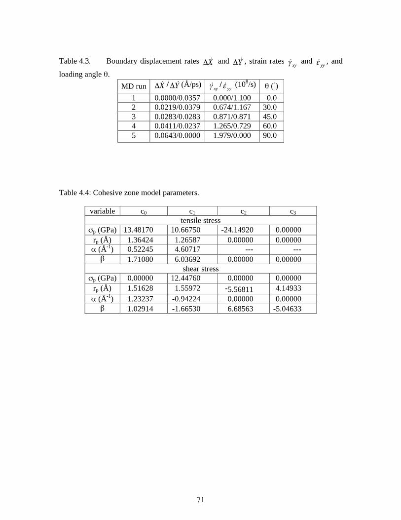
71
Table 4.3. Boundary displacement rates X&! and Y&! , strain rates
xy!& and
yy!& , and
loading angle θ. MD run X&! / Y&! (Å/ps)
xy!& /
yy!& (108/s) θ (◦)
1 0.0000/0.0357 0.000/1.100 0.0 2 0.0219/0.0379 0.674/1.167 30.0 3 0.0283/0.0283 0.871/0.871 45.0 4 0.0411/0.0237 1.265/0.729 60.0 5 0.0643/0.0000 1.979/0.000 90.0
Table 4.4: Cohesive zone model parameters.
variable c0 c1 c2 c3 tensile stress
σp (GPa) 13.48170 10.66750 -24.14920 0.00000 rp (Å) 1.36424 1.26587 0.00000 0.00000 α (Å-1) 0.52245 4.60717 --- --- β 1.71080 6.03692 0.00000 0.00000
shear stress σp (GPa) 0.00000 12.44760 0.00000 0.00000
rp (Å) 1.51628 1.55972 -5.56811 4.14933 α (Å-1) 1.23237 -0.94224 0.00000 0.00000 β 1.02914 -1.66530 6.68563 -5.04633

72
Fig. 4.1: Pair energy function curves for different pairs.
Fig. 4.2: Cohesive energy as a function of lattice constant.

73
Fig. 4.3: Geometry of molecular dynamics simulation.

74
Fig. 4.4 Shear loading boundary conditions.

75
Fig. 4.5. Schematic of regions used to calculate (a) global and (b) local properties.

76
Fig. 4.6. Tensile stress as a function of (a) true normal strain; and (b) normal
boundary displacement obtained under pure tensile loading condition θ = 0◦.

77
Fig. 4.7. Shear stress as a function of (a) shear strain; and (b) shear boundary
displacement obtained under pure shear loading condition θ = 90◦ .

78
Fig. 4.8. Crack length as a function of time.

79
Fig. 4.9. Stress and opening as functions of x coordinate obtained at a mixed loading
condition of θ = 45◦. (a) normal stress and normal opening; and (b) shear stress and shear opening.

80
Fig. 4.10. (a) local normal stress as a function of crack local normal opening under
mode I fracture; and (b) local shear stress as a function of crack local shear opening under mode II fracture.

81
Fig. 4.11. Comparison of the σp, rp, α, and β MD data with analytical prediction. (a)
σp; (b) α; (c) rp; and (d) β.

82
Fig. 4.12. Comparison of stress σ as a function of crack opening Δr between MD
data and fitted curves. (a) ψ ~ 1.3◦; (b) ψ ~ 30.2◦; (c) ψ ~ 46.7◦; (d) ψ ~ 60.4◦;
and (e) ψ ~ 86.8◦. ψ is defined as !!
"
#
$$
%
&
'+'
'22
2
yx
xArcSin .

83
Fig. 4.13. Stress σ as a function of crack opening components Δx and Δy. (a) normal
stress; and (b) shear stress.

84
Fig. 4.14. Work of separation as a function of loading condition ψ.

85
5. Summary
We have demonstrated that patterned, nanoscale interfacial roughness can increase the apparent interfacial toughness of a brittle, thin-film material system. In one set of tests, nano-imprint lithography was used to create a rectangular-toothed pattern of 60-nm wide by 90-nm deep channels on a silicon surface. A highly compressed, 280-nm thick tungsten film was deposited on top of this surface. The width of the buckles that formed indicates that the apparent toughness of the patterned interface is 50% higher than that of a similarly prepared system with an atomistically smooth interface. Detailed finite element simulations of a thin film bimaterial strip with a rectangular-toothed channel interface pattern identified those factors that influence the apparent interfacial toughness. The finite element results indicate that the interface does not unzip in a continuous manner. Instead, the crack-tip is stalled as it tries to kink in a direction that is perpendicular to its original path. Cracks then initiate on those segments of the interface that are at the end of the tungsten and silicon teeth. Ultimately, the sidewalls fail in shear. The apparent interfacial toughness was found to scale directly with real interfacial area. The apparent interfacial toughness also scales directly with a figure of merit that compares interfacial strength,
!
ˆ " , to a measure of the stress needed to open a crack at the tip of a tooth once cracking initiates. This segment cracking stress, σc, varies as (E*Γo/a)1/2 were E* depends on the mismatch in film/substrate elastic properties, Γo is the intrinsic interfacial toughness, and a is the characteristic length scale of the pattern. Apparent toughness tends to increase with increasing
!
ˆ " /"c as segment failure becomes
more abrupt and brittle-like. The increased energy dissipation is associated with a more dynamic failure process that generates kinetic energy, which would ultimately be converted to thermal energy. Molecular dynamic simulations were used to investigate the fundamental nature of atomic scale interfacial separation processes under mixed mode loadings. These atomistic simulations used generic interatomic potentials and incorporated a brittle interface. Calculated results suggest that the intrinsic work of separation in shear is a factor of two higher than in normal separation. In contrast, finite element interfacial separation models typically assume that there is no intrinsic variation in separation energy with the mode of loading.

86
Distribution: 1 Professor David Barr
Washington State University School of Mechanical and Materials Engineering PO Box 642920 Pullman, WA 99164-2920
1 Professor Marty Dunn University of Colorado at Boulder Department of Mechanical Engineering Campus Box 427 Boulder, CO 80309-0427
1 Professor Molly Kennedy Clemson University 113 Olin Hall
Clemson, SC 29634 1 Professor Kenneth Liechti
University of Texas at Austin Aerospace Engineering & Engineering Mechanics 210 E. 24th Street, WRW 110C 1 University Station C0600 Austin, TX 78712-0235
1 Professor Ray Pearson Lehigh University 5 East Packer Ave. Bethlehem, PA 18015 1 Professor Zhigang Suo Harvard University
School of Engineering and Applied Sciences Room 309, Pierce Hall 29 Oxford Street Cambridge, MA 02138
3 MS 0346 E. D. Reedy, Jr., 1526 1 MS 0372 J. M. Redmond, 1525 1 MS 0372 J. Pott, 1524 1 MS 0847 P. J. Wilson, 1520 1 MS 1070 C. C. Wong, 1526 1 MS 1070 Day file, 1526 1 MS 1245 J. A. Emerson, 2453

87
1 MS 1315 M. J. Stevens, 8332 1 MS 1411 M. E. Chandross, 1814 3 MS 9402 X. Zhou, 8776 1 MS 9404 E-P Chen, 8776 1 MS 9042 J. W. Foulk, 8776 3 MS 9402 N. R. Moody, 8758 1 MS 9409 J. A. Templeton, 8757 1 MS 9409 G. J. Wagner, 8757 1 MS 9049 R. E. Jones, 8776 3 MS 9409 J. A. Zimmerman 8776 1 MS 0123 D. Chavez, LDRD Office, 1011 2 MS 0899 Technical Library, 9535 2 MS 9018 Central Technical Files, 8944
![1 Interfacial Rheology System. 2 Background of Interfacial Rheology Interfacial Shear Stress Interfacial Shear Viscosity = [ ]](https://static.fdocuments.us/doc/165x107/56649d1f5503460f949f3d29/1-interfacial-rheology-system-2-background-of-interfacial-rheology-interfacial.jpg)