EEEN 204 Assignment 1 2021
17
1 EEEN 204 Assignment 1 2021 Below are the problems for this assignment. Do your calculation as needed and then type your final answers as well as the discussion or plots in the spaces required. Submit this document with a filename: EEEN202_Assmt1_2020_”your surname”-“your initial” on the Wiki submission system. (4) Due: Monday 19 July 11.59 pm. Name: Model Answers Student Number:………………………………………………………………………………. Question Marks Obtained Filename 2 Q1 21 Q2 6 Q3 5 Q4 4 Q5 11 Q6 9 Q7 12 Q8 10 Q9 10 Total 90
Transcript of EEEN 204 Assignment 1 2021
1
EEEN 204 Assignment 1 2021
Below are the problems for this assignment. Do your calculation as needed and then type your final
answers as well as the discussion or plots in the spaces required. Submit this document with a
filename:
EEEN202_Assmt1_2020_”your surname”-“your initial” on the Wiki submission system. (4)
Due: Monday 19 July 11.59 pm.
Name: Model Answers
Student Number:……………………………………………………………………………….
Question Marks Obtained Filename 2
Q1 21
Q2 6
Q3 5
Q4 4
Q5 11
Q6 9
Q7 12
Q8 10
Q9 10
Total 90

2
Q1) Multiple Choice: Choose the answer that you would see as the best correct description of the
statement. You should then explain why you chose this answer. (Hint: “Because it is the best
answer” will not be sufficient).
(i) Semiconductors are useful as electronic devices because (1)
They are very abundant in nature
They are all good conductors
They have a very high melting point
x Their electrical conductivity can be controlled by the addition of impurities
Their electrical conductivity can be controlled by a variation in the temperature
Explain why you chose this answer: (2)
Yes are abundant and yes temperature influences conductivity but most importantly they provide us
with the ability to control conductivity (magnitude and type) by means of impurities.
(ii) The magnitude of the electronic bandgap in a solid is primarily determined by (1)
The temperature
The number of free electrons in the material
x The nature and strength of the chemical bond in the material
The type of doping in the material
Will decrease when we apply a positive voltage
Explain why you chose this answer: (2)
Chemical bond dominant, effect of temperature just secondary

3
(iii) The number of intrinsic carriers in a semiconductor (1)
x Will be determined by the temperature and the bandgap of the material
Is always greater than the extrinsic concentration
Is always less than the extrinsic concentration
Is determined by the doping level in the material
Will determine the conductivity of the material
Explain why you chose this answer: (2)
The intrinsic concentration depends exponentially on both the size of the bandgap (inversely) and on
the temperature
(iv) When doping a semiconductor n type, the bandgap of the material will: (1)
Increase
Decrease
x Remain the same
Will decrease when we apply a negative voltage
Will decrease when we apply a positive voltage
Explain why you chose this answer: (2)
Doping will not change the size of the bandgap unless doped to extremely high levels.

4
(v) When doping a semiconductor p type, the bulk of the material has: (1)
A positive charge
A negative charge
x Is neutral
Will only get a positive charge when we apply a voltage
Explain why you chose this answer: (2)
Material will always remain neutral after doping
(vi) In order to generate free charge carriers by optical excitation, the wavelength of the incident
light needs to be: (1)
Monochromatic (single wavelength)
Longer than the cut-off wavelength of the material
x Shorter than the cut-off wavelength of the material
Of a very high intensity to penetrate the material
Explain why you chose this answer: (2)
Shorter than cut-ff wavelength implies higher energy than the badgap.

5
(vii) Light of the correct wavelength to produce optical excitation is incident on a piece a p-type Si.
This will produce: (1)
A greater number of holes than electrons
A greater number of electrons than holes
A greater change in the number of holes relative to the number before illumination
x A greater change in the number of electrons relative to the number before illumination.
Explain why you chose this answer: (2)
The number of holes and electrons produced by the incident light will be equal. However, compered
to the relative number of holes and electrons in the material before the process, the increase in
minority carriers (electrons in this case) will be far greater than the increase in holes (majority
carriers).

6
Q2) (a) Calculate the electrical conductivity of copper if it is given that the metal has 8.5 x 10²²
conduction electrons per cm3 and the mobility of a conduction electron is 35 cm2.V-1.s-1. (3)
Answer: 4.76 x 10⁵ Units (Ω.cm)-1
(b) In an electronics project you need to construct your own inductor. The instructions for making
this inductor is to “wind it from a 1.2 meter length of # 20 AWG (American wire gauge) copper wire.
(i) How thick is this wire in mm ? (1)
Answer: 0. 812 mm
Look up AWG sizes
(ii) What will be the resistance of your inductor ? (2)
Answer: 4.9 x 10⁻²Units Ω
7
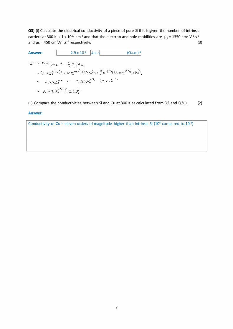
Q3) (i) Calculate the electrical conductivity of a piece of pure Si if it is given the number of intrinsic
carriers at 300 K is 1 x 1010 cm-3 and that the electron and hole mobilities are μe = 1350 cm2.V-1.s-1
and μh = 450 cm2.V-1.s-1 respectively. (3)
Answer: 2.9 x 10⁻⁶ Units (Ω.cm)-1
(ii) Compare the conductivities between Si and Cu at 300 K as calculated from Q2 and Q3(i). (2)
Answer:
Conductivity of Cu ~ eleven orders of magnitude higher than intrinsic Si (105 compared to 10-6)

8
Q4) Following on from Q3, the temperature now increases to 350 K. Describe semi-quantitatively
how and why the carrier concentration and the conductivity will change due to this temperature
change for both these two materials (Si and Cu). (4)
Answer:
With an increase in temperature the conductivity of the copper will decrease while the conductivity
of the Si will sharply increase. This is due to the fact that in the case of the Cu the number of charge
carriers remain relatively constant, but the carrier mobility actually decreases due to increased
scattering at higher temperatures. In the case of Si we will have a exponential increase in intrinsic
carrier concentration with temperature, leading to sharply increasing conductivity.

9
Q5) (a) Silicon is doped by adding As atoms to a level of 5 x 10¹⁵ As atoms/cm3. Calculate:
(i) the concentration and type of majority carriers (3)
Answer Concentration: 5 x 10¹⁵ Units cm-3
Answer Type: n-type
(ii) the concentration and type of minority carriers (3)
Answer Concentration: 2 x 10⁴Units cm-3
Answer Type: p-type
(iii) Calculate the conductivity of this doped silicon. (3)
Answer: 1.08Units (Ωcm)-1
(iv) How does the conductivity of the doped Si compare to the undoped (intrinsic) Si in Q3. (2)
Answer:
Approximately six orders of magnitude higher (100 compared to 10-6) for the doped material

10
Q6) The sketch below shows the band diagram of a doped semiconductor, indicating several charged
species present in this material. The densities of these charged species are not represented to scale.
Now answer the following questions on this diagram.
(i) Is this material p-type or n-type ? (1)
Answer: p-type
(i) What is the origin of the negatively charged centres within the bandgap ? Are these charged
centres mobile or stationary when we apply an electric field ? (2)
Answer:
These negative charges are due to the acceptor atoms from the impurities added for doping.
These atoms (from Group 13) will accept an electron and thus be negatively charged. They are not
free to move as they are locked in by bonding from surrounding Si atoms.
(ii) What is the origin of the positively charged holes in the valence band ? Are these positive charges
mobile or stationary when we apply an electric field ? (2)
Answer:
The holes in the valence band come from the missing electrons that had been accepted by the
acceptor impurities. These charges can move when an electric field is applied.
(iii) What is the origin of the negatively charged electrons in the conduction band ? Are these
negatively charged electrons mobile or stationary when we apply an electric field ? (2)
Answer:
These are intrinsic (thermally excited) electrons. Free to move in an electric field.

11
(iv) What is the relative energies (order of magnitude) for the values of Eg and EA ? (2)
Answer:
Eg in order of 1 eV, Ea at least 10 X smaller in order of 0.1 eV
12
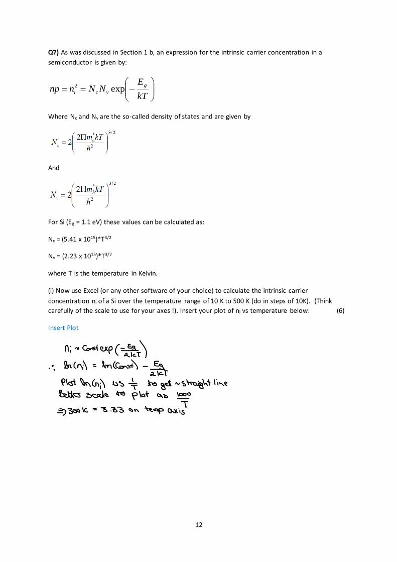
Q7) As was discussed in Section 1 b, an expression for the intrinsic carrier concentration in a
semiconductor is given by:
−==
kT
ENNnnp
g
vci exp2
Where Nc and Nv are the so-called density of states and are given by
And
For Si (Eg = 1.1 eV) these values can be calculated as:
Nc = (5.41 x 10¹⁵)*T3/2
Nv = (2.23 x 10¹⁵)*T3/2
where T is the temperature in Kelvin.
(i) Now use Excel (or any other software of your choice) to calculate the intrinsic carrier
concentration ni of a Si over the temperature range of 10 K to 500 K (do in steps of 10K). (Think
carefully of the scale to use for your axes !). Insert your plot of ni vs temperature below: (6)
Insert Plot

13
(ii) Consider the semiconductors Ge (Eg = 0.7 eV) and GaAs (Eg = 1.4 eV) and assume that the same
values of Nc and Nv will hold as for Si (not really true !). Calculate approximate values for ni for these
two semiconductors at temperatures of 80 K, 300 K and 400 K and compare to the values obtained
for Si at these temperatures. Also calculate the expected electrical conductivity of each of the three
semiconductors at 300 K. (6)
Calculated values for ni and σ:
Semiconductor Ni at 80 K Ni at 300K Ni at 400 K σ at 300 K
Si ~0 1 x 1010 cm-3 3 x 1012 cm-3 2.9 x 10⁻⁶ (Ω.cm)-1
Ge ~0 5 x 1013 cm-3 2 x 1015 cm-3 4.6 x 10⁻² (Ω.cm)-1
GaAs ~0 3 x 107 cm-3 4 x 1010 cm-3 4.3 x 10⁻⁸ (Ω.cm)-1
Assuming the same vales of hole and electron mobility for GaAs and Ge as we had for Si we get:
4
6
8
10
12
14
16
18
2 2.5 3 3.5 4 4.5 5
LOG
(NI)
1000/T (K^-1)
Si GaAs Ge

14
If we ask Google for the typical values of electron and hole mobility in GaAs and Ge we get:

15
Q8) Now consider a piece of Si doped n-type to 5 x 1015 cm-3. The carrier concentration is measured
over a temperature range from just above 0K to about 1000K and the result is plotted as ln(n) vs T(K)
as in the graph below. For each of the point 1 to 5 on the graph explain the behaviour of n at this
point by considering the process of carrier generation. (10)
Answer:
1. 0K or close to it with all carriers frozen out at these low temperatures.
2. As temperature increases we start to excite electrons from the donor levels into the conduction
band. As the value of Ed is very small, this happens at very low temperature.
3. All the donor levels has now been emptied and the electrons excited into the conduction band.
The material thus behaves as extrinsic over a wide temperature range and the carrier concentration
remains constant over this range
4. However as the temperature keeps increasing the intrinsic carrier concentration will keep
increasing due to thermal excitations. At some point these intrinsic carriers will exceed the number
of extrinsic carriers and we will see a rise in the number of free carriers. The number of carriers will
rise exponentially due to the intrinsic carriers now dominating at high temperatures.
5. Seen as point where material transitions from extrinsic to intrinsic

16
Q9) (i) A semiconductor has a direct energy gap of 1.5 eV. Calculate the expected optical cut-off
wavelength of this material. (2)
Answer: 0.83Units µm
(ii) Light with a wavelength between 200 and 1500 nm is incident on a wafer of this material. Sketch
the expected transmission spectrum of the material over this wavelength range and clearly indicate
in what part of the spectrum we would expect electron-hole pairs to be formed by the incident light.
(4)
When wavelength is shorter than 830 nm the light will all be absorbed by the semiconductor as yhe
energy of the light is > the energy of the bandgap. AS the energy falls below the gap we will have
sharp transition to all light transmitted.
(iii) On the same plot as (ii) also plot the expected transmission spectrum if this material should
have an indirect bandgap.
(2)
(iv) Explain the difference in optical absorption between direct and indirect bandgap
semiconductors. (2)
Answer:
Absorption in the indirect bandgap material is much more inefficient as the electrons require both a
change in momentum and in energy. We will then not see the strong absorption just above the
bandgap that we se in a direct bandgap semiconductor.

17
*****