EEE458 VLSI II Laboratory Laboratory Module 7:...
16
Department of Electrical & Electronic Engineering Bangladesh University of Engineering & Technology EEE458 VLSI II Laboratory Laboratory Module 7: Silicon Compilation using Cadence SOC Encounter Objectives: The following Cadence CAD tools will be used in this tutorial: •SOC Encounter for backend design (floor planning, place and route, power and clock distribution). (1) For this lab make a directory lab7pnr in the cds_ius directory. For this Lab you will copy the following 6 files i.e. map.conf, map.v, map.io, map.sdc, vtvtlib25.tlf, vtvtlib25.lef files from the following directory home/eda/Cadence/Common_Files/enc_25u From the lab7pnr directory type: encounter The command encounter (no &) starts SOC Encounter in the foreground and you should get the encounter startup window: The window has three main areas: • Menu Bar (top) • Select Bar (right) • Display Area (middle)
Transcript of EEE458 VLSI II Laboratory Laboratory Module 7:...

Department of Electrical & Electronic Engineering Bangladesh University of Engineering & Technology
EEE458 VLSI II Laboratory
Laboratory Module 7: Silicon Compilation using Cadence SOC Encounter
Objectives: The following Cadence CAD tools will be used in this tutorial: •SOC Encounter for backend design (floor planning, place and route, power and clock distribution). (1) For this lab make a directory lab7pnr in the cds_ius directory. For this Lab you will copy the following 6 files i.e. map.conf, map.v, map.io, map.sdc, vtvtlib25.tlf, vtvtlib25.lef files from the following directory home/eda/Cadence/Common_Files/enc_25u From the lab7pnr directory type: encounter The command encounter (no &) starts SOC Encounter in the foreground and you should get the encounter startup window:
The window has three main areas: • Menu Bar (top) • Select Bar (right) • Display Area (middle)
©ABM H. Rashid, Dept. of EEE, BUET Page 2 8/02/2014
Please try to familiarize yourself with the main window, click on the menus, on the Toolbar widgets, etc. For more information on the various Cadence tools I encourage you to read the corresponding manuals. You can get to the menu reference manual for Encounter by pressing Help on the right of the Menu Bar.
Now we can start using Encounter. First we need to import the synthesized netlist (the result of RTL synthesis with RTL Compiler). Click on File Import Design and the Design Import window should pop-up. Now you need to fill in the Verilog netlist (use the browser button on the right to navigate to your synthesized netlist, in this case map.v, make sure you click on Add. Now click Top Cell By user and type CHIP as top cell. Next click the Load button of the design import window and click on map.conf and click OK. Make sure that the following appears.
If you have LEF files, enter the names of the files. You must specify the technology LEF file first, then specify the standard cell LEF and block LEF in any order.
Then we need to specify the timing definitions for the library, do that by clicking on the navigate button on the right of the Common Timing Libraries entry which should pop-up the Timing Files window (note that more advanced libraries will have Max Timing and Min Timing Libraries in order to be able to do "corner analysis", not just nominal analysis). Example of such file is stdcellxxx.tlf file. Unfortunately we do not have such file at possession and hence we will sip this.
For a full chip design, we would also have to specify the I/O pad information. This information have been described in the IO Assignment File which is map.io ins this case.
©ABM H. Rashid, Dept. of EEE, BUET Page 3 8/02/2014
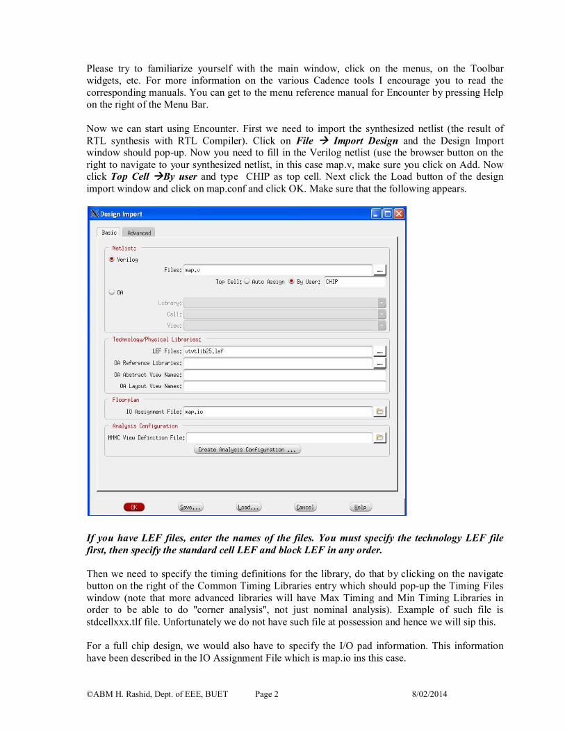
Now click on the Advanced tab at the top followed by Power on the left. You will see that vdd and vss are automatically filled in by the configuration file.
Finally click on OK in your Design Import pop-up window. Get familiar with some of the widgets, for example the Design Browser widget (the 7th from the right, top row) lets you see the design hierarchy, etc.
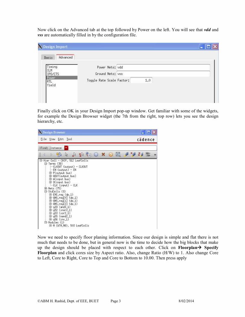
Now we need to specify floor planing information. Since our design is simple and flat there is not much that needs to be done, but in general now is the time to decide how the big blocks that make up the design should be placed with respect to each other. Click on Floorplan Specify Floorplan and click cores size by Aspect ratio. Also, change Ratio (H/W) to 1. Also change Core to Left, Core to Right, Core to Top and Core to Bottom to 10.00. Then press apply
©ABM H. Rashid, Dept. of EEE, BUET Page 4 8/02/2014
Click on Apply and the floor plan should change to reflect the 100 micron periphery around the core.
The following floor plan appears. Now you can also play with the aspect ratio on the Specify floor plan window, change that to 0.5, click Apply, then to 2, click Apply again, finally back to 1 and click Apply. Note how the number of rows in your floor plan changes from 5 (for 1) to 7 (for 2) to 3 (for 0.5). It is a good idea to save your design from time to time by File Save Design chip.enc
©ABM H. Rashid, Dept. of EEE, BUET Page 5 8/02/2014
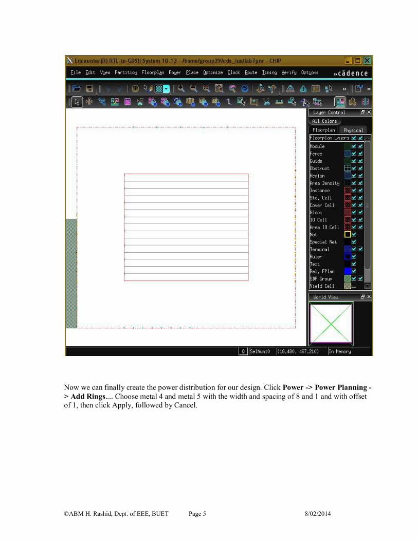
Now we can finally create the power distribution for our design. Click Power -> Power Planning -> Add Rings.... Choose metal 4 and metal 5 with the width and spacing of 8 and 1 and with offset of 1, then click Apply, followed by Cancel.

©ABM H. Rashid, Dept. of EEE, BUET Page 6 8/02/2014

©ABM H. Rashid, Dept. of EEE, BUET Page 7 8/02/2014
Click Power -> Power Planning -> Add Stripes.... Choose metal 2 with the width and spacing of 2 and 5 respectively and with X from left of 20, then click Apply, followed by OK.

©ABM H. Rashid, Dept. of EEE, BUET Page 8 8/02/2014
Then, in order to route the rest of the power distribution click Route -> Special Route..., deselect Pad pins, then click Apply, followed by OK.

©ABM H. Rashid, Dept. of EEE, BUET Page 9 8/02/2014
Now your floor plan should look like this.
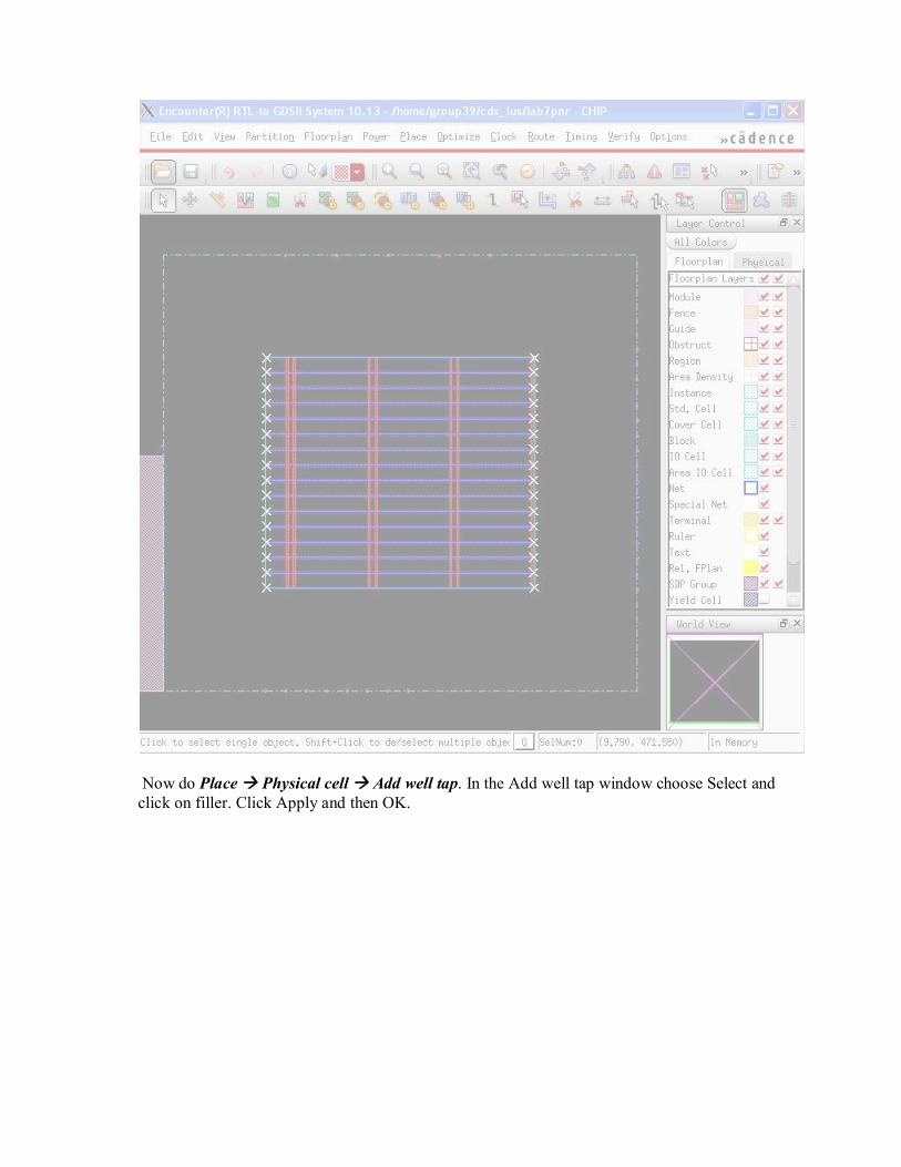
Now do Place Physical cell Add well tap. In the Add well tap window choose Select and click on filler. Click Apply and then OK.

©ABM H. Rashid, Dept. of EEE, BUET Page 11 8/02/2014
It is time to place our cells, go to Place Place Standard Cell... then click Apply, followed by OK.
The layout should look like this
©ABM H. Rashid, Dept. of EEE, BUET Page 12 8/02/2014
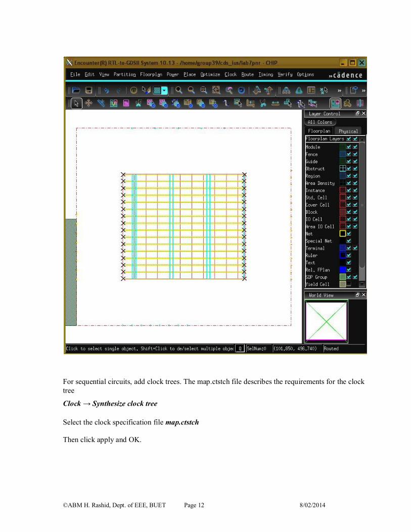
For sequential circuits, add clock trees. The map.ctstch file describes the requirements for the clock tree
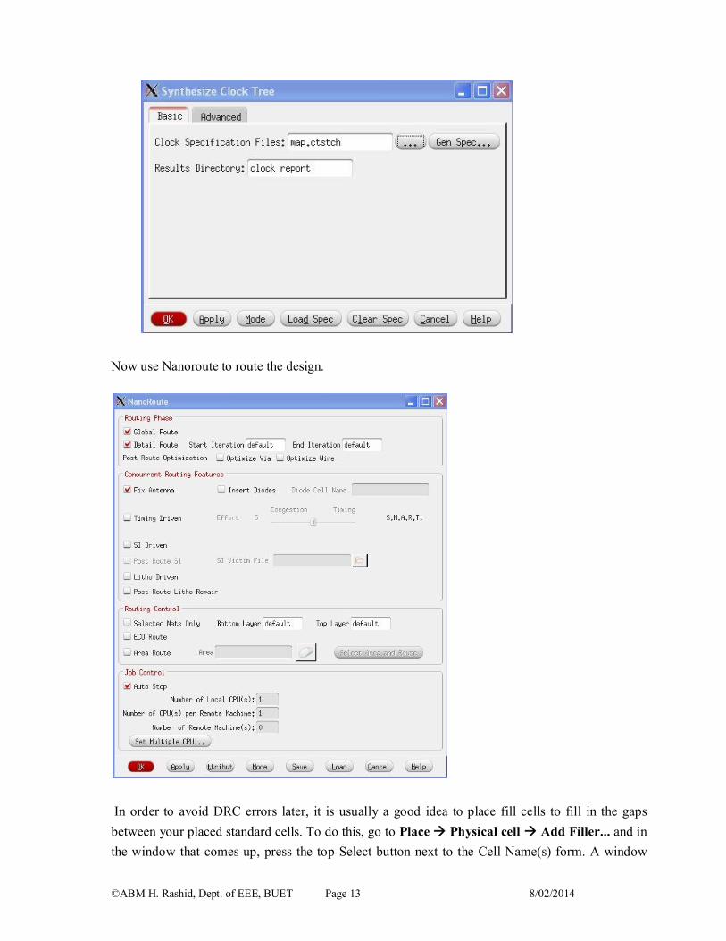
Clock → Synthesize clock tree Select the clock specification file map.ctstch Then click apply and OK.
©ABM H. Rashid, Dept. of EEE, BUET Page 13 8/02/2014
Now use Nanoroute to route the design.
In order to avoid DRC errors later, it is usually a good idea to place fill cells to fill in the gaps between your placed standard cells. To do this, go to Place Physical cell Add Filler... and in the window that comes up, press the top Select button next to the Cell Name(s) form. A window

©ABM H. Rashid, Dept. of EEE, BUET Page 14 8/02/2014
will pop up and in the right column you should see a line that says filler. Select filler from the right side, click Add followed by OK. In the Add Filler window you should now see filler in the top form. Click Apply followed by OK.
Now Route Metal fill Add After metal fill of empty space, the layout will look like this

©ABM H. Rashid, Dept. of EEE, BUET Page 15 8/02/2014
Now that you have completed the physical design of your circuit it is a good idea to verify it by running a DRC check. To do this in SoC Encounter, select Verify -> Verify Geometry... and then click OK. Make sure there are no violations listed in the terminal window.
You will get the verification results in the bash shell window. Similarly verify Connectivity.

©ABM H. Rashid, Dept. of EEE, BUET Page 16 8/02/2014
Log of verify geometry in encounter.
Thus you have finished Place and Route and completed your layout. Now File Save Design CHIP.enc click OK. Again save the design in Design Exchange Format (DEF). Fil Save DEF
Congratulations, this is the end of the Silicon on Chip (SoC) Encounter Lab.
Report : 1. Provide the layout diagram of your finished circuit and result of Geometry and Connectivity
Verification result. 2. Now make the Place and Route of your project and show it to the instructor.