eecs.ucf.edueecs.ucf.edu/.../g18/Content/SeniorDesign1FinalDocument.docx · Web viewI will first...
213
Department of Electrical & Computer Engineering University of Central Florida MaRC S-Park Magnetic Resonance Coupling with Sophisticated Parking Group F Steven Pyle Brendan Oliver Jimmy Lee
Transcript of eecs.ucf.edueecs.ucf.edu/.../g18/Content/SeniorDesign1FinalDocument.docx · Web viewI will first...

Department of Electrical & Computer EngineeringUniversity of Central Florida
MaRC S-Park Magnetic Resonance Coupling with Sophisticated Parking
Group FSteven Pyle
Brendan OliverJimmy Lee
Nick Martinez

Table of Contents:
1. Executive Statements 11.1 Executive Summary 11.2 Motivations 21.3 Goals 31.4 Objectives 4
2. Specifications and Requirements 52.1 Power Supply 52.2 RF Power Signal 52.3 Magnetically Coupled Resonators 62.4 RF Power to DC Power 72.5 Capacitor Array 72.6 Data Acquisition 8
2.6.1 Microcontroller 82.6.2 Wireless 92.6.3 High Voltage Management 9
3. Research 93.1 Similar Projects and Products 9
3.1.1 Inductive Wireless Power 93.2.2 Witricity 10
3.2 Power Supply 103.2.1 Voltage Regulation 11
3.2.1.1 Linear Regulator 123.2.1.2 Switching Regulator 133.2.1.3 Step Transformer 15
3.2.2 Rectifiers 173.2.2.1 Diodes 173.2.2.2 Power Diodes 183.2.2.3 MOSFETs 193.2.2.4 Power MOSFETs 19
3.2.3 Resistors 203.2.3.1 Power Resistors 203.2.3.2 Capacitors 21
3.3 RF Power Signal 213.3.1 Oscillators 22
3.3.1.1 Crystal Oscillators 223.3.1.2 Oscillator Circuits 233.3.1.3 Voltage-Controlled Oscillator 253.3.1.4 Programmable Oscillators 25
3.3.2 RF Amplifier 263.3.2.1 Class A Amplifier 263.3.2.2 Class C Amplifier 27

ii
3.3.2.3 Class D Amplifier 283.3.2.4 Class E amplifier 29
3.3.3 Gate Driver 303.3.4 Conclusion 30
3.4 Magnetically Coupled Resonators 313.4.1 2-Coil Resonators 363.4.2 4-Coil Resonators 36
3.5 RF Power to DC Power 373.6 Capacitor Array 373.7 Data Acquisition 43
3.7.1 Programmable systems other than a Microcontrollers 433.7.2 Microcontrollers 46
3.7.2.1 Basic Architectures 463.7.2.1.1 Von Neumann/ Princeton 473.7.2.1.2 Harvard 473.7.2.1.3 Modified Harvard 483.7.2.1.4 Wrap up of Relevance 48
3.7.2.2 Microcontroller Research 493.7.2.2.1 Texas Instruments 503.7.2.2.2 Microchip 513.7.2.2.3 Atmel 523.7.2.2.4 Infineon 543.7.2.2.5 NXP 553.7.2.2.6 Parallax 56
3.7.3 Peripherals/Sensors/Displays/Communications equipment 563.7.3.1 Wireless Communications 563.7.3.2 Voltage Sensors 57
3.7.3.2.1 High voltage issue 583.7.3.2.2 Observing Voltage Input 583.7.3.2.3 Observing Load Output 58
3.7.3.3 Regulating Output 583.7.3.4 Graphical User Interface 593.7.3.5 Programming the Microcontroller 59
3.7.4 Data Acquisition Software and Language 593.7.4.1 Programming the Microcontroller 603.7.4.2 Other Software 60
4. Design 614.1 Design Power Supply 61
4.1.1 Specifications 614.1.2 Design 624.1.3 Schematics 634.1.4 Components 63
4.2 RF Power Signal 654.2.1 Programmable Oscillator 65

iii
4.2.1.1 Specifications 654.2.1.2 Components 664.2.1.3 Conclusion 67
4.2.2 Class E Power Amplifier 674.2.2.1 Specifications 674.2.2.2 Design 674.2.2.3 Schematics 694.2.2.4 Components 71
4.2.2.4.1 Transistor 714.2.2.4.2 Inductors 724.2.2.4.3 Capacitors 74
4.2.2.5 Conclusion 744.2.3 Gate Driver 75
4.2.3.1 Specifications 764.2.3.2 Components 764.2.3.3 Conclusion 77
4.3 Magnetically Coupled Resonators 774.3.1 2-Coil Resonators 794.3.2 4-Coil Resonators 81
4.4 RF Power to DC Power 824.4.1 Design 824.4.2 Specification 824.2.3 Schematic 834.4.3 Components 83
4.5 Capacitor Array 844.5.1 Capacitor Protector Circuit 914.5.2 LED Low Voltage Warning 98
4.6 Data Acquisition 101 4.6.1 32-bit Microcontroller 102 4.6.1.1 Contenders 102 4.6.1.1.1 Competitors I 104 4.6.1.1.2 Competitors II 105 4.6.1.1.3 Competitors III 105 4.6.1.1.4 Microcontroller of Choice 106
4.6.2 High Voltage Sensor configuration 1074.6.3 Wireless communication network 109
4.6.3.1 XBee 1094.6.4 Display real-time data 1104.6.5 Regulate load discharge output 1124.6.6 Short circuit charging process 1134.6.7 Alert low voltage in capacitors 1134.6.8 Data Acquisition Budget 114
5. Design Summary 1145.1 Power Supply 114

iv
5.2 RF Power Signal 1155.3 Magnetically Coupled Resonators 1215.4 RF Power to DC Power 1225.5 Capacitor Array 1235.6 Data Acquisition 1245.7 PCB Board 125
6. Testing 1256.1 Power Supply 1256.2 RF Power Signal 126
6.2.1 Functionality Testing 1266.2.2 Prototype Testing 126
6.3 Magnetically Coupled Resonators 1266.4 RF Power to DC Power 1286.5 Capacitor Array 1286.6 Data Acquisition 129
7. Prototype Construction 1307.1 Bill of Materials 1317.2 Procurement 1327.3 PCB 132
7.3.1PCB Manufacturing Foundries 1337.3.2 PCB Software 133
7.4 Assembly 134
Appendix A) Permissions aA.1 Wikipedia aA.2 UBM LLC (DesignNews.com) cA.3 Vishay Siliconix cA.4 Texas Instruments d
Appendix B) Figures eAppendix C) References g

1. Executive Statement
1.1 Executive SummaryThe project that will be presented in this design documentation is for a project based on technology first conceived by the great Nikola Tesla in his pursuit of designing a method of energy distribution which would revolutionize the distribution of electrical power. The technology spoken of is none other than the technology of wireless power, a concept so cutting edge at the time of Nikola Tesla’s creative spark, with the Wardenclyffe tower, that it was summarily suppressed as an idea until the time of William C. Brown in 1964 when research on the topic began to return to the possibilities of engineers. Concepts of this have been thrown around for the application of this technology, but with low efficiency as attempts to create electromagnetic fields to carry the power is the primary methodology used in these systems. This is a project to prove the concept so long ago sought, as a viable method of transporting electricity at high power outputs.
Primarily, the project’s objective is to build a system of which rapid recharge is achieved and can be used in a duration significantly longer than the time taken to charge the load. It will take an input power (outlet power) and translate it to a carry-able signal (AC-DC-AC) through a set of inductors in coupling, and charge an ultra-capacitor array (AC-DC) which can be used as a containment system for the load. The load itself is a remote control car. This was chosen for the fact that the automotive applications are high as a means to innovate electric car technology by eliminating the need for relatively long charge times as well as the need to plug in and instead of plugging in, to simply drive over an inductive pad to recharge (a set it and run concept).
But, the reason why this project intrigued us is that it would provide a practical use for both wireless power and a low cost ultra-capacitor array since wireless power is typically tough to achieve with the need for high efficiency hinging on the need for a high coupling ratio. Another reason for pursuing this project is that it is a fascinating concept, since the majority of technology that is electrically based requires a power cord or power source of its own. The power signal strength would depend heavily on the distance between the inductors to achieve effective coupling. Ultra-capacitor output would decide the amount of energy that could be stored, requiring a circuit to be responsible with maintaining output levels, giving a high capacity with regulated voltage and current output.
Imagine getting power without the need for a bulky transformer attached to a phone which is powered by a paper thin inductor connected to a small full wave rectifier that feeds the phone the power it needs. This project would prove the feasibility of electronic technologies that cannot utilize a power cord, or where charge time is not a limiting factor of the ergonomic uses of ultracapacitor

2
technologies attached to a simple AC-DC conversion circuit, or even show that wireless power can be an effective means of charging/recharging systems connected to an inductor coil in magnetic resonance coupling. It is an endeavor that could be backed by Progress Energy as an alternative power distribution method, an important concept with energy companies as distribution is just one opposite side of the whole power industry. Progress is the primary electricity provider for the parts of Florida, South Carolina, and North Carolina. We hope to prove that this technology is but one feasible use of these technologies currently on market.
1.2 MotivationThe reason why we pursue such an unproven technology to base our design around is because the technology holds a great potential for innovation. This technology would reduce tremendously the material costs accrued by manufacture of wired transmission. Those resources can then be repurposed for more pertinent uses. On another hand, the system could also provide a highly practical/ergonomic use for wireless power as a quick and easy car charging method, even if it solely is for recreational car use (toy cars). The argument is that one primary hindrance for the avocation of electric car technology is that it is impractical with too little power output and an impractically long charging time for little applicable use as well as the need for a wired infrastructure. We live now in a time and age where gratification must come quickly and time is a major factor to the considerations of the individual who wants to make the most of their second. This could satisfy the needs of those people with a more environmentally friendly electrical system that harnesses the power of a singular source rather than have multiple sources creating the same volume of energy at a tremendously higher impact upon the environment.
There also is an explanation for the use of ultracapacitors, primarily based around the physical principles of a capacitor versus a battery. A battery is good for applications where voltage regulation is important, as they tend to regulate energy output by chemistry rather than electrical properties of metals. Though batteries hold an advantage of being very simple to use, they lack the electron flow speed which rapid recharging requires. The usage life on batteries as well is an important factor of why capacitors are used over batteries. The chemistry of a battery tends to break down over time in the form of lost charge capacity (internal impedance) or physical corrosion of the cell itself. A capacitor on the other hand can theoretically have a running lifetime of nearly 100 times more cycles. A battery may be able to run over 100 or 1000 times, but ultracapacitors could theoretically cycle hundreds of thousands of times. This could be a highly advantageous medium for energy storage.
As a group, the purpose of the project is so we can better understand how these recent technologies and apply an impressive method of their usage. Wireless power and Ultra-capacitors are relatively new to the technology fields with few

3
applications as of yet. The purpose is to understand their use and possible places which these technologies can be used in other uses. But, as a proof of concept, this project will couple the two parts together. The project will require the use of data collection, experimental technology, and tried and true concepts within the field of electrical engineering. The application of the skills in the programming of microcontrollers, power systems, and hardware design will be tested. Data and hardware linking will be utilized with the hope to better understand the duties of an engineer.
1.3 GoalsThe aim of this project is simple to design, prototype, and test a working and practical wireless charger utilizing Ultra-capacitor and inductive resonance coupling technology. To do this, there are three goals to accomplish, the effective signal boosting from wall power 120V 60Hz to at least 24V 10 MHz, resonance coupling, and charge and discharge management of capacitors and its accompanying circuitry. The overall goal is to have as high efficiency as possible with this project and that requires the goals above.
With regards to the signal boosting, it will require more than just the simple oscillator crystal. This is a step which is paramount in maintaining a higher efficiency for later portions of this design. The 120V to at least 24V will bring down the useable energy to a useable level while the frequency increase will bring up the stability of the signal. This way, the signal can be strong enough for an efficiency level between 100% and 50%, anything below could be deemed too low for practical purposes.
Resonance coupling is the second factor that is important to the application of wireless power. It determines the transmission efficiency from one side to the other side of the inductor within the inductor resonance. The aim for this portion is for around 75% -65%. To achieve this, the inductors must be digitally calibrated to be able to space the inductor coils at the proper gap to find the best resonance coupling distance, thereby making the most effective use of the magnetic fields formed by the inductors.
The capacitor array is the last major goal of this project. This will be where the efficiency pays off, where the energy collected can be calculated with regard to charge time. What the priority of this part is to be able to have a regulated discharge and a quick, as near to instantaneous, charging speed. Again, like the 120V 60Hz to 24V 10 MHz conversion, it requires more than just a simple circuit. This portion though will more than likely require a digital controller, but ultimately needs to be capable of charging quickly and discharging at a controlled wattage.By the end, the goal is to prove that these technologies have an important use in the technology of the future. Scalability will be an overall goal for this project as well since the technology at hand is important and has applications at all levels of scale from micro-electronics to automotive; from home appliances to industrial

4
power distribution applications. Scalability will also be able to serve as the longevity of this project model, as it expands the basis of which the applicability of the research placed into this project can cover. Though the project does not reach the scope of encompassing many different types of applications, the use of both together is a milestone on its own by proving the worth of their abilities. The better we can implement and understand these technologies, the better and cleaner the future will hopefully be and the better we will understand the state of current technologies.
In a more abstract goal, it will aid in preparing those who follow through with the project with a better abstract understanding of project based work and the nature of the work environment with the stress and politics which accompanies it. It will in the end improve our overall ability to problem solve in the industry and the real world, as well as the technology is better.
1.4 Objectives (In list organization)There are a few key points that must be achieved through this project:AC voltage drop – This step is to bring the voltage down to a useable level that the inductor coils can use for the purpose of creating a magnetic field to allow for coupling. This will be important for the protection of the circuits in the system and to lower the physical constraints that limit cost effective designing of the system.
AC frequency boosting – The second parameter of alternating current is to allow for a strong magnetic coupling. As the frequency rises, the better gain and distance are achievable. When the frequency is lower, the strength of the signal degrades at distance. To design a high frequency system would improve the gain and inductor gap allowed in the resonance coupling system.
Inductive Resonance Coupling tracking – Since the magnetic field fluctuates ever so slightly as the system is active, the optimal efficiency air gap can be theoretically tracked to find the right distance on to get the optimal efficiency. This will then allow for the maximal efficiency of the inductor system.
Electrical data collection – The collection of data is important for the tracking of the system efficiency of the wireless charging system. The data can be used to feed digital controllers information to actuate the inductor air gap, and hone in on the correct distance between the inductors coils to maximize the efficiency of the coil pair. This also is important in understanding the feasibility of these technologies
Fast recharge - This objective is to define the time efficiency of the use of ultracapacitors. It ties in with the next objective of this project.

5
Regulated Recharge – This is important for maintenance of the capacitor array and protection of capacitors, load, and inductor system as well as AC to DC circuitry.
Capacitor Discharge Regulation – There should be a workable time frame with the use of ultra-caps. This will be compared with the recharge time and should be proportionally larger time span compared to the recharge time.
Display of Real-Time Values in Systems – This is to allow for real-time tuning of inductive coupling air gap for maximum efficiency.
Load output – if there becomes additional time on the project. The complexity of the load can be increased, adding portions and features that will ramp the difficulty of the project up.
2. Specifications and Requirements
2.1 Power SupplyIn order to determine the specifications and requirements of the power supply, we must first determine the requirements for the rest of the project in order to understand how much power the power supply is going to need to power, and at what voltages.
With the other parts of the project designed, we have determined the specifications and requirements of the power supply to be as follows.
2 railso 1 at 30V for the class E amplifier, and it must be able to handle up
to 5 amps.o 1 at 5V for the integrated circuits on the station, such as the MCU
and the programmable oscillator. The current draw for this rail is quite small.
Receives 120V at 60Hz from a standard wall outlet. Voltage ripple is not a major concern for our project, but it should be no
greater than 5%.
2.2 The RF Power Signal GeneratorFor our project, the design of the RF power signal generator is critical, as it's performance will have a massive impact on the performance of the resonators, the efficiency of the entire design, and the power transferred ultimately to the RC car.

6
Our best estimates to our designs require that our signal be about 10 Megahertz, so our RF power signal generator should be able to generate a range of signals centered around 10MHz. Another key consideration is to consider the method of transferring the power; in our project, we will be using magnetically coupled resonators, and current is a critical factor in magnetic coupling. When there is a greater current passing from the transmitting resonator to the receiving resonator, the coupling will be greater, and therefore the better the efficiency. For this reason the RF power signal should be able to generate a signal of at least one amp of current. These specifications are summarized below.
Generate a range of frequencies from 1MHz to 20MHz on the fly for tuning Generate at least 1A of current RMS at 20-30 volts RMS The higher the efficiency the better
The RF power signal generator will require simply a dc source from the power supply to power the amplifier, the gate driver, and to power the oscillator. The requirements are summarized below.
30 volts DC at a max of 5 amps for the amplifier 5 volts DC for the gate driver as well as the oscillator
2.3 Magnetic Coupled ResonatorsThe Magnetic Coupled Resonators are used to deliver power to the capacitor array once it’s over the wireless charging pad. The point of this component is to allow us to transfer power to the car without any direct contact, hence wireless charging, but it must be sufficient enough to deliver power reliably, efficiently, and quickly to the capacitor array. As such, the MCRs (Magnetic Coupled Resonators) have several requirements to meet the following standards.
Small form factor. The MCR network must not interfere with the normal operation of the car through physically obstructing the car’s path, rendering the car unable to travel where it would other be able to travel, or any other means of physical interference.
Electronically stable. The MCR network must not interfere with the normal operation of the car through electromagnetic interference, such as blocking signals to be received from the control mechanism, disrupting power to be transmitted to capacitor array or the car, or by otherwise causing the car’s electrical systems to malfunction.
Reliable. The MCR network on the car must be able to receive a reasonable amount of physical trauma and withstand the elements without ceasing to function. It must also remain in place so as not to misalign itself when placed over the charging mechanism, which is highly sensitive to displacement.

7
High Power. The MCR network must be able to delivery at least 30W of power to the capacitor array, ideally 50W. It must also maintain a high degree of efficiency by neither consuming nor losing too much electric energy in the process of transmitting it.
The MCR network is to be supplied with a 20+V AC, 10MHz signal. It is to transmit at least 15V AC, 10MHz successfully to its receiving end so as to successfully power the capacitor array with little to no issues. The more power delivered, the better, and the 15V AC requirement is a bare minimum, 20-25V AC would be more ideal.
To gain the maximum amount of efficiency, the MCR network will have its size manufactured such that it takes advantage of the exact gap between the two planar inductors which will transmit power in our network. To take advantage of the MCR concept, the resonant frequency of both the transmitter and receiver will be set to 10MHz, and will be designed to have an exceedingly high Q value in order to maintain a great deal of efficiency.
2.4 RF to DC Power SupplySince the power going into the RC car from the receiver coil is at RF frequencies, special considerations must be taken to account for such high frequencies when converting it to DC. The determined specifications and requirements are as follows.
Be able to convert a range of frequencies to 15V DC from 1MHz to 20MHz AC
Be able to handle currents up to 3 Amps Voltage ripple is not a huge concern, but it should be no greater than 5%
2.5 Capacitor ArrayThe Capacitor Array is going to be used to power our RC car. We decided to go with a capacitor array as opposed to a standard battery pack to ensure quick charging, so as to easily demonstrate our wireless charging of the RC car. Leaving a battery pack in would take far too long to be able to demonstrate the device to a panel. Supercapacitors allow us to charge quickly and to store large amounts of energy. The Capacitor array must adhere to the following conditions:
Able to hold at the absolute minimum 6V worth of charge. The more, the better.
Able to dispense at least 1.5A of current, as per the requirement of the RC car, and the ability to hold this 1.5A current for an extended period of time

8
Low ESR (Equivalent Series Resistance) to allow for quick charging without overheating or damaging the capacitors
Small form factor. If they are too large, the capacitors will disrupt regular functions of the RC car.
Lightweight. Large amounts of weight will require more power from the motor. More power means less run time.
Reliability. The capacitors are worth very little to us if they cannot be used to repeat our tests a significant number of times, and replacing them is just another source of frustration for any potential clients.
High peak current output. Higher peak current output means the capacitors will be able to supply the car with enough power to allow the car to keep operating, even when there is a large, sudden load from the car. Such loads occur when the car is attempting to perform a sharp turn and accelerate at the same time.
The capacitors will be powered by a DC power source of at least 15V. To avoid being charged to overvoltage, the capacitors must also be protected by a protector circuit. These protector circuits will shut-off the charging mechanism to the capacitor once it has reached a threshold voltage. For our purposes, the capacitor array will more than likely have an 8.1V rating with an 8.5V absolute maximum. Therefore, to ensure the safety of our group, the observing panel, and our group, as well as the continued success of this project, our protector circuit will stop charging at 8V. This circuit will use a comparator along with a voltage reference of 8V to determine when a switch will be opened.
2.6 Data Acquisition ParametersThe parameters required for the data acquisition portion of the project are at minimum for the microcontroller needs, wireless requirements and high voltage management for discharge and charging.
2.6.1 Microcontroller1. A minimum number of 20 I/O2. Compatibility with the use of I2C connectivity3. Clock rate to allow for effective and real-time use of a display4. LCD usability5. ACD resolution minimum of 10-bits6. Power consumption of microcontroller of less than 5V7. 2 comparators.8. Connectivity to extensive peripherals9. Minimum of 128k Memory10. Less than $100 microprocessor and hardware11. Low cost software12. Respectably sized user community

9
13. Experienced user language (MIPS, C-code, etc.)14. Wireless peripheral compatibility15. Control of digital peripherals
2.6.2 Wireless:1. Low cost (under $20 per unit)2. Zigbee or IEEE 802.15.4 standard3. Unused frequency to communicate (ex. 2.4GHz or 886MHz)4. Low powered (3.3V Max)5. Minimum range of 100 Feet6. Does not interfere with inductor resonance frequency (10MHz)7. 10-bit resolution minimum
2.6.3 High Voltage Management:1. ADC components with as high definition as possible2. Methods to reduce voltage and current to manageable levels.3. Secondary circuit’s in-case of overload (circuit fuse, rerouting, or shunts)
3. Research
3.1 Similar Projects and ProductsWith the emergence of wireless charging pads that charge your mobile devices, a plethora of consumer products have been developed to fill the market. In this section, we will be taking a look at these products as well as Witricity. Witricity is a new and emerging technology which is essentially the same thing that we are doing, the wireless transfer of power via magnetically coupled resonators on planar coils. Therefore it would be quite wise to take a look into this technology to help with our own project.
3.1.1 Inductive Wireless PowerInductive charging is a very near field, within the range of 1cm to 2cm, wireless power transfer technology. It’s also very inefficient even at very close ranges. Regardless of these disadvantages, it’s quite widespread in use due to its small footprint and ease of production. It’s found in a variety of applications such as RFID chips, implanted devices, and the wireless charging stations introduced to the market a few years ago that wirelessly charge your mobile devices.

10
It’s interesting to compare inducted wireless power transfer technology to the magnetically coupled wireless power transfer technology that we are working on in this project. Magnetically coupled wireless power transfer technology is a much farther field power transfer technology when compared to inductive charging. The magnetically coupled resonators can transfer power quite efficiently at ranges up to a meter. This puts it into a whole other realm of applications compared to inductive wireless transfer technology. You can use magnetically coupled resonators to wirelessly charge a car as it’s parked, something that inductive wireless power transfer could never do, nor do at efficiencies in the ranges of magnetic coupling.
The main advantage inductive wireless power transfer technology has over magnetically coupled resonance wireless power transfer technology is that right now magnetically coupled resonators are quite bulky; the systems generally developed and studied today utilized a drive loop, a resonator coil, a receiver coil, and a load loop. What Witricity has developed and we are essentially replicating is to consolidate all of those coils into just one planar transmission coil, and one planar receiver coil. Inductive wireless power transfer technology also operates at much lower frequencies than magnetic coupling resonance, which makes it easier to design power systems to drive the inductance.
3.1.2 WitricityWitricity is a company which manufactures products for wireless power transfer using strongly coupled magnetic resonators. This technology is extremely similar to our project, and I would even go as far as to say that they are exactly the same, except that our main purpose is demonstrate the ability to wirelessly charge electric vehicles. Witricity has demonstrated the ability to power a 60 watt light bulb from 2 meters away, even when the light of sight was blocked with a wooden panel. They have also demonstrated the ability to power a television wirelessly. All of this is a good demonstration as to the validity to our project, as we are only looking to transfer about 30 watts to wirelessly charge a capacitor array on an RC car.
3.2 AC/DC Power SupplyThis project design calls for a steady, strong and reliable Direct Current (DC) signal that will introduce very minimal if not any oscillations. This, in turn, requires a source of mains and its conversion from Alternating Current to DC. In our design, we will implement this technique via a power supply designed around the necessary specifications required. In recent years, similar projects have considered many topologies such as Full Wave Rectifier Diode Bridge in low frequency applications. Using the positive half cycle of an oscillating input signal to charge a smoothing capacitor and dissipate only some of its energy during the negative half cycle of the input signal to a parallel load streaming the output

11
voltage. In even more recent years, these diodes have been substituted for more efficient components such as MOSFETs, more particularly, Power MOSFETs.
The whole idea of using Power MOSFETS, and will be considered in the design portion, is related to
1. Power MOSFETs in forward active mode will have very little forward voltage drop as compared to the 2N2222.
2. The Linear Active mode Resistance from Drain to Source is close to nothing and can be advantages when high current output is needed.
3. Power MOSFETS have a considerably fast switching time (for the time it takes to reverse the bias in the FET and no longer allow the flow of current through the component.
As we get closer to today’s day in age, the demand for the right power supply has shifted. More economical solutions to power supplies are taken into consideration with lower wattage requirements and intuitive techniques. Our means of power for this project in turn must remain economical in a way such that our power consumption is on average with commercial power supplies available today.
Moreover, as power supplies has been and always will be a component in which the engineer and consumer must be aware of the dangers that come along with manufacturing and use of this product, protection has been implemented such that if the supply is quickly removed from its source there will be a means of power dissipation and “cutoff” of feedback current negatively affecting the integrated circuit components. This is one of the major considerations in on both our design and power supplies in general, due to the destruction not only the integrated circuits but a possible threat to user/consumers health.
Our design calls for considerable protection which may involve different techniques such as diodes that cut off feedback current, Zener diodes to regulate the voltage across transistor components such as a MOSFET to insure that the Drain to source voltage does not exceed the maximum threshold requirements, heat sinks if the power dissipation amongst components becomes too high, and fuses to protect against current becoming relatively too high.
3.2.1 Voltage RegulationVoltage regulation is one of the most important aspects of this project simply because this is where it all begins. The foundation of our power supply that will enable our overall goal will be to obtain a reliable and economical source of DC power. This pure DC signal will provide more than just power and so it must be done in careful consideration of the proceeding components, their requirements and specifications.

12
3.2.1.1 Linear RegulatorOne of the ways in which we have considered initially regulating the voltage is to use a linear regulator. This will simply regulate an incoming voltage signal down to the specified voltage (specification done by the manufacture) and the difference in voltage will be burned off into a heat sink attached to the regulator itself. One condition must remain constant when using the Voltage Regulator is that the difference in input voltage and output voltage must be more than the drop off voltage (referenced in each Voltage Regulator’s Datasheet).
Linear regulators also have attribute that are disadvantageous. To start with the most obvious this method isn’t the most efficient nor is it the economical. To show this, take consideration maybe you have a 5V regulator available and you wanted to test this out with an input voltage of 15V. As efficiency, or gain as in electronics, is defined:
Efficiency=Output VoltageInput Voltage
∗100 %
If you apply this equation, you will see that the voltage regulator only achieves a transfer efficiency of 33.33%. Our project and applications frowns upon this method because if we must apply the same principle we will obtain 25% efficiency.
One thing that we must also consider is the fact is that our project input signal is AC not DC. The polarity on a Voltage Regulator is not meant to be switched. In doing so the user may damage the integrated circuit permanently especially if the Voltage Regulator was not properly protected with reverse protection diodes.
Given below is an example of a Linear Voltage Regulator with an AC input and the resultant output in 3.2.2.1 Figure 1 and 2 respectively. This implementation shows that with an AC current, once the voltage is above the drop off voltage the, input is regulated to 5 volts. Once the output drops below the drop off the output almost immediately drops to zero and the negative half cycle is rectified. Standing wave will exist without the presence of the inductor and its impedance suppressing them. Moreover, the capacitance cannot be charged fully and fast enough to store energy and dissipate it over the load constantly if we chose to use this design as then rectifier.

13
Figure 3.2.2.1-1: Multisim Schematic of Linear Voltage Regulator with Alternating Current Input
Figure 3.2.2.1- 2: Multisim Output Voltage of Linear Voltage Regulator with Alternating Current versus Time
3.2.1.2 Switching RegulatorThe switching regulator, a lot like the Linea Voltage Regulator but is more efficient when efficiency is critical like power management as in our project’s power supplies. The output voltage can be adjusted such that the regulator doesn’t have to burn so much energy off. This economical advantage is rather useful and has absorbed a lot of our consideration. Furthermore, the Switching Regulator will, a majority of the time use bypass capacitors from input to ground

14
and output to ground to really diminish the amount of noise on both sides but this comes with a cost. If the Switching Regulator is suddenly cut off from its input voltage spikes can occur resulting in reversing the bias on the regulator, again, resulting in permanent damage of the integrated circuit chip. One last consideration is that we are still using an AC input signal so this method may not be beneficial to our project in terms of regulation in voltage.
3.2.1.2 Figures 1 and 2 show an example of a switching regulator with an AC input and its output respectively. The switching regulator can obtain the gain needed but cannot maintain the charge long enough across the capacitor to quickly keep the load discharging for rectification use. Furthermore, this does not produce a stable stepped down AC signal and is no longer a possibility for converter design.
Figure 3.2.1.2-1: Switching Voltage Regulator with and Alternating Current Input

15
Figure 3.2.1.2-2: Output of Switching Voltage Regulator with Alternating Current Input. Output shows unstable AC signal with no rectification.
3.2.1.3 Step TransformersStep up and step down transformers are a completely different spin on voltage regulation. The transformer’s output in AC is a ratio of the number of turns on the primary voltage side to the number of turns on the secondary voltage side. The equation below shows this relation,
VoltageSecondaryVo ltagePrimary
=Number of Turns SecondaryNumber of TurnsPrimary
which is derived from Faraday’s Law. The ideal transformer doesn’t allow any energy to be wasted. One important note to keep in mind when dealing with a transformer is that since there is no significant change in resistance, then by Ohm’s Law, the current much change to keep the law consistent. This is not only true but also very applicable to our project application. Not only will we be able to regulate the voltage down to our feasible work means, but we are also boosting the current when the voltage drop occurs. This can play a big role in how our capacitive array will function in terms of charging time and efficiency.

16
3.2.1.3 Figures 1 and 2 below show a perfect example of the step down required with stability.
Figure 3.2.1.3-1: Step down Transformer with a Two to One Turn Ratio. Expected Output Voltage to be Half the Input.

17
Figure 3.2.1.3 - 2: The 2:1 Step Down Transformer Output Displaying Proper Step Down with Stability (Channel A: Input Voltage =120Vrms Channel B: 59.98 Vrms)
3.2.2 RectifiersIn any AC to DC converter there is in some way shape or form the rectification of an alternating current signal into a direct current power source by means of rectification. By rectification we can establish the DC power signal necessary to power our whole design. The process of rectification is a simple task but can become more complex depending on the following factors:
How much power dissipation the designer does and does not want amongst different components
Which components the designer would like to use in addition to or in replace of others
If the designer wishes to eliminate some noise or reduce the noise to an absolute minimum
And how much Voltage and current is needed for further component specification and requirements.
3.2.2.1 DiodesDiodes are the most common way for rectifying any alternating current signal. The 1N4000 series, very commonly used P-N junction diodes, work excellent for half wave and full wave rectification, and AC to DC conversions. The forward voltage drop on these diodes range from 0.65V to 1 V and have a DC blocking potential of up to 1000V. Needless to say the AC to DC converter design will not need such extreme blocking, but its principle use is its contribution.
3.2.2.1 Figures 1 and 2 show an example using 1N4000 series diodes at high current of 3 Amps and output respectively.

18
Figure 3.2.2.1-1: Diode Bridge with Smoothing Capacitor.
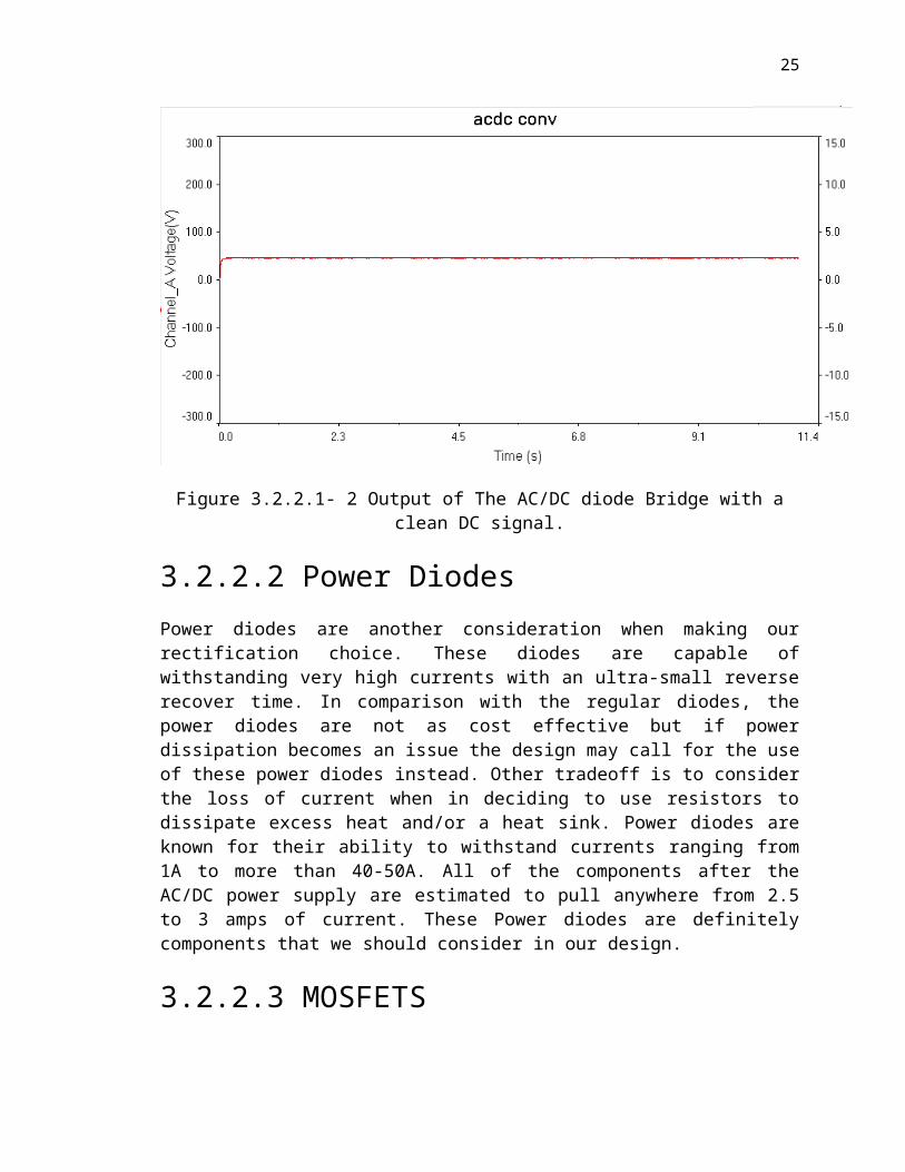
Figure 3.2.2.1- 2 Output of The AC/DC diode Bridge with a clean DC signal.
3.2.2.2 Power DiodesPower diodes are another consideration when making our rectification choice. These diodes are capable of withstanding very high currents with an ultra-small reverse recover time. In comparison with the regular diodes, the power diodes are not as cost effective but if power dissipation becomes an issue the design may call for the use of these power diodes instead. Other tradeoff is to consider the loss of current when in deciding to use resistors to dissipate excess heat and/or a heat sink. Power diodes are known for their ability to withstand currents ranging from 1A to more than 40-50A. All of the components after the AC/DC

19
power supply are estimated to pull anywhere from 2.5 to 3 amps of current. These Power diodes are definitely components that we should consider in our design.
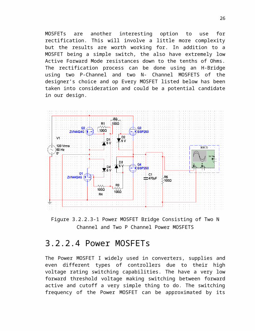
3.2.2.3 MOSFETSMOSFETs are another interesting option to use for rectification. This will involve a little more complexity but the results are worth working for. In addition to a MOSFET being a simple switch, the also have extremely low Active Forward Mode resistances down to the tenths of Ohms. The rectification process can be done using an H-Bridge using two P-Channel and two N- Channel MOSFETS of the designer’s choice and op Every MOSFET listed below has been taken into consideration and could be a potential candidate in our design.
Figure 3.2.2.3-1 Power MOSFET Bridge Consisting of Two N Channel and Two P Channel Power MOSFETS
3.2.2.4 Power MOSFETsThe Power MOSFET I widely used in converters, supplies and even different types of controllers due to their high voltage rating switching capabilities. The have a very low forward threshold voltage making switching between forward active and cutoff a very simple thing to do. The switching frequency of the Power MOSFET can be approximated by its input impedance, which it generally low in the milliohms to the tens of Ohms, and the input capacitance which can be found in the specific datasheet of the component. This RC relation can also

20
approximate if not give the upper operating frequency limit in which gives insight into to the Power MOSFET’s frequency response. The frequency response will play an important role in our power supply design if we decide that using MOSFETs in the rectification process is the best implementation due to the capacitive properties of the MOSFETs relative to the following:
Overall size of the Power MOSFET The material used in the MOSFET gate separation. Depending on
whether the material is a poly-silicon gate or more of a pure metal oxide will affect the overall input impedance slightly adjusting the switching time and upper limit on operating frequency range.
The distance between the Drain and the Source and how this distance relates to the capacitive value
The orientation of the MOSFET, e.g. using a Vertical DMOS Power FET versus using standard P or N Channel MOSFET of a certain size. This also is a contribution to the previous point above about the capacitance relative to the distance between the Drain and the Source.
3.2.3 Resistors
In many of the considered designs, resistors play a significant role in many ways and though simulations may not take what material the resistors are into account our project will. The ideologies behind using different types of resistors are:
The material used in the resistor may not be able to withstand the power demands of the supplies in terms of voltage, current and power requirements.
The actual impedance of the resistor must be high enough to eliminate noise enough for a clear signal but not to overkill the design by dissipating to much heat or taking too much voltage that is required for the remaining circuitry.
Beyond the specifications of the power supplies, many voltage division must be made such as comparator designs will function according to the project requirements
The different materials that we will look at will be look into in other sections. As far as the power supplies, we will consider only one type of resistors besides our tradition ceramic and metal oxide resistors and films.
3.2.3.1 Power ResistorsThe power resistor will be a very important contribution in meeting the specifications and requirements of the power supplies involved in our project. Power resistors will enable the power supply to safely dissipate heat and withstand the current requirements. Most of the metal oxide films and ceramic

21
resistors commonly used today are rated at only a 0.25-0.5 Watts of power. This means that, for example if we wanted to have a resistive element with impedance of 2000 Ohms, then this means we can only pass a current of 0.25 milliamps. This is wattage doesn’t even scratch the cusp of the necessary wattage needed to power the rest if this happen to be the load impedance of the supply voltage. At a current of 3 Amps, this 2000 Ohms ceramic or metal oxide resistor will inevitable catch on fire, damaging other integrated circuits and possibly hurting an individual.
This problem is solved by using low impedance, high power resistors that will by far be able to stand up to the requirements of our project.
3.2.3.2 Capacitors
Capacitors have many uses in the power supply design of our project. The major role that they may play in our project will be the following:
Filtering out any noise from the final DC power signal output The “smoothing’ technique referenced in the diode bridge. The capacitor
will charge and discharge in the positive and negative half cycles, respectively, of the sinusoidal input to remain a constant voltage across the load at the output.
The size of the capacitance relative to the frequency to maintain constant voltage drop across the output load.
3.3 RF Power SignalIn order to wirelessly transmit power from the transmission coil to the receiver coil via magnetically coupled resonators, we must drive the coils with a very high frequency. According to papers detailing previous work on magnetically coupled wireless power transfer, this range is generally within 1MHz to 10MHz. The efficiency of the wireless power transfer is dependent upon the resonance of the transmission and resonator coils, the distance between them, and the frequency of the signal powering the system. Although we could derive the optimum frequency to drive the coils and then base the signal generating stage to generate a signal of that frequency, it would be much more flexible and easier to “tune” if we develop a signal generating stage that could generate a wide range of signals as efficiently as possible.
Upon researching the generation of high frequency power signals, which is a popular topic in RF transmission, it has been determined that the best course of action is to generate a low power, high frequency signal, and then amplify that signal to the required current levels in order to generate enough flux between the transmission and receive resonators.

22
General Objectives:· Develop a stand-alone oscillator, that is easy to adjust and that can generate a wide range of frequencies from at least 1MHz to 10MHz· Develop an efficient amplifier that can drive the oscillator signal up to sufficient current levels in order to produce enough flux in the transmission coil to induce the magnetic resonance in the receiver coil to efficiently transmit power to the RC car.
The following sections detail the various methods to generate high frequency signals and their corresponding advantages and disadvantages and then how to efficiently amplify those signals to our desired power ranges.
3.3.1 OscillatorsIn the following sections, we will be discussing the various methods of generating a high frequency signal at least in the range of 1MHz to 10MHz; further consideration will be taken to generate signals up to 20MHz just for the flexibility and to help alleviate the inadvertent troubles that develop from taking designs from paper to prototype, that is, have some wiggle room for the inevitable losses that will be incurred when we develop the physical prototype. We will be focusing on stability, efficiency, complexity of design, requirements, feasibility of implementation and tuning, and the strength of the output signal.
3.3.1.1 Crystal OscillatorsA Crystal Oscillator Circuit utilizes the mechanical resonance effects of certain piezoelectric materials to create an electrical signal with a very precise frequency. A crystal oscillator can be modeled as an electric RLC circuit, such as in figure 3.1:
Figure 3.3.1.1-1 Equivalent Crystal Oscillator Circuit (Permission: Wikipedia)
Crystal Oscillators can be used to within circuits as a high Q RLD tank to generate a signal in various circuits such as the Pierce Oscillator in figure 3.2:

23
Figure 3.3.1.1-2 Pierce Oscillator (Permission: Wikipedia)
We can also use a crystal oscillator in the positive feedback of an op-amp to drive it to oscillation in resonance with the crystal device.
The advantages of using crystal oscillators is that they have a very high Q-factor, in the order of 4 to 6 orders of magnitude, compared to generally 2 orders of magnitude for LC oscillators. This is desirable for a very precise, stable signal, but greatly hinders the range in which crystal oscillators can operate over. Crystals are also very resilient to changes in temperature.
For our project, we want to be able to design the signal generator to operate over a wide range of frequencies because it is much easier to adjust such a signal generator than to remanufacture the transmitter and receiver plates. Since we cannot completely pre-determine the resonant frequency of the plates, a wide band signal generator would allow us to tune to the actual physical resonant frequency of the plates. For this reason, crystal oscillators aren’t a very good option because they have such a limited range of frequencies of which can be adjusted without completely redesigning the circuit with a different crystal.
3.3.1.2 Oscillator CircuitsLC oscillator circuits are similar to the crystal oscillators in that they use a tuned circuit to resonate at a particular frequency, but as opposed to a piezoelectric material fulfilling the tuned circuit duties, an LC “tank circuit” is used to drive the circuit into resonance. These are very well studied and quite easy to design. Some common LC oscillator circuits are the Hartley oscillator shown in figure 3.3.

24
Figure 3.3.1.2-1 Hartley Oscillator (Permission: Wikipedia)
Another popular possible oscillator circuit that would fulfill our oscillator needs is the Colpitts oscillator depicted in figure 3.4.
Figure 3.3.1.2-2 Colpitts Oscillator (Permission: Wikipedia)
One last oscillator researched was the Clapp oscillator, which is a rather simple and robust design and is depicted in figure 3.3.1.2-3.
Figure 3.3.1.2-3 Clapp Oscillator (Permission: Wikipedia)
Although LC oscillators have a much lower Q-factor and are more subjective to fluctuations in temperature when compared to crystal oscillators, they make up for this in their simplicity, easibility in tuning, and their wide range of possible frequencies with just the use of a variable capacitor. This makes this option especially attractive to our project because a change in the oscillation frequency would just require changing a capacitor.

25
One thing to be careful of with these circuits is to make sure that the active devices in them are capable of handling our high frequency needs. Many op-amps, BJTs, and MOSFETs cannot handle being driven at such high speeds, and therefore special care and consideration needs to be taken into choosing such a device if we choose to use an LC oscillator for our initial signal generation before the power stage.
3.3.1.3 Voltage-Controlled OscillatorsVoltage-Controlled Oscillators, or VCOs, are common off the shelf oscillator devices that do a great job of generating a wide range of frequencies based upon a voltage applied to the circuit. They are generally used for generating signals for various communication transmission schemes such as frequency, and phase modulation, but can be easily adopted to generate the frequencies required for our project. There are both VCOs which utilize op-amps, as well as crystal oscillators, which both have their strengths and weaknesses similar to the oscillators discussed in 3.3.1.1, and 3.3.1.2.
Crystal VCOs have very high Q-factors, and such are very stable and accurate, but lack a wide range of producible frequencies, although it is possible to generate more signals from the division of such frequencies, this over complicates our design for our project and still lacks and fine tuning ability between the divided frequencies.
Op-amp based VCOs are inherently less stable and precise, but the range of producible signals is much greater. This makes this a more attractive option for our project compared to the crystal-based voltage controlled oscillator because it’s more important for us to generate a greater range of frequencies than having an extremely stable signal; the stability of these op-amp based VCOs is plenty for our project.
One thing to consider when determining to use a voltage controlled oscillator is how you are going to control it. Would it be a rotary potentiometer, an analog output from a microcontroller, or a digital signal from a microcontroller to a digital to analog converter to the VCO.
3.3.1.4 Programmable Oscillators
Programmable Oscillators are great little integrated circuits similar to VCOs in that they are able to produce a wide range of frequencies without changing components, but they are programmable in the sense that a serial input can control the output frequency. They are generally used to generate clock signals for processors and other digital circuits.

26
The frequency they produce can be adjusted via a serial input from a microcontroller, which greatly simplifies the process of controlling a voltage controlled oscillator from a microcontroller. Since we will be having a microcontroller in our designs to measure various currents, powers, and efficiencies throughout our design, it wouldn’t be difficult to have it adjust a programmable oscillator to drive the wireless power transmission via some onboard interface.
Something to consider with programmable oscillators is that they generally produce square waves at their output. That means if we are to use certain amplifier designs which are best driven via a sinusoidal input, we must have a low pass filter after the programmable oscillator in order to convert the square wave to a sinusoidal wave. Certain amplifier design, however, are actually driven quite well from a square wave, and therefore makes the programmable oscillator even more attractive if one of those designs is determined best suited for our project.
3.3.2 RF AmplifierDriving high frequency signals to the range of 20 to 30 watts requires a unique set of solutions compared to lower frequency signals such as audio. From section 3.3.1, we have a selection of signal generation methods which all provide small power outputs in the range of microwatts to a milliwatt. These signals are not strong enough to drive RF power MOSFETS into saturation, or even into linear mode; therefore, we must consider designing and implementing a driver amplifier or pre-amplifier to drive the small signal into levels usable to drive the large RF power MOSFETS used in the power amplifier stages. We will be discussing Class A, C, D, and E amplifier designs because these designs are the most common when dealing with RF frequencies. Then we will discuss what we have determined the best course of action for the amplification of the signal to our desired power levels.
3.3.2.1 Class A AmplifierClass A amplifiers are designed to be driven entirely in the linear mode of the transistor. This is achieved by applying a biasing voltage to the base-emitter for BJT or gate-source junction for a MOSFET. This provides a very clean, highly linear, and undistorted amplified signal at the collector. The general topology of the class A amplifier can be found in figure 3.3.2.1-1.

27
Figure 3.3.2.1-1 Class A Amplifier (Permission: Wikipedia)
The problem concerning this type of amplifier is that it's extremely inefficient, to the extent of well below 50% efficiency. Aside from the large power loss due to this design, it would also dissipate huge amounts of heat and need a method of cooling the active device. All things considered, a class A amplifier would be a poor choice for the main power amplification stage of our RF power amplifier, but it could be a great choice for an earlier driver stage due to its linear operation, the fact that you don't want to cause too much distortion early in the amplification of the RF signal, and the power and heat dissipation would be negligible due to the very small signal being amplified in the early stage.
3.3.2.2 Class C AmplifierClass C amplifier design is a tuned amplifier in which conducts during a small portion of the signal. In a class C design, the active element only conducts during a small portion of the input signal, and therefore the period of time that current is flowing and there is a voltage drop across the base-emitter or source-drain is minimized; this minimizes the power dissipated by the transistor. Theoretical efficiencies can be up to 100%, but real devices cannot pass infinite current over an infinitesimally small time, so realistic efficiencies are around 75%.
In order to keep the signal going during the off-portion of the device, class C amplifiers generally have a tuned output circuit to resonate with the desired frequency. Due to the tuned nature of the design, it is not applicable to wide band applications, and has to be tuned to the particular frequency desired to be transmitted. This is not an issue if we have a chosen operating frequency for the magnetic resonance, but can be an issue if we want to vary the frequency significantly. The tuned nature of the design also allows the transistor to only have to conduct for a small portion of the signal, and therefore increases the efficiency dramatically. The general topology for the class C amplifier, excluding the output LC tank circuit is shown in figure 3.3.2.2-1.

28
Figure 3.3.2.2-1 Class C Amplifier (Permission: Wikipedia)
3.3.2.3 Class D AmplifierClass D amplifiers are a high efficiency design which utilizes MOSFETs as switches to output pulses of power in relation to the input signal of the amplifier. Class D designs are generally more complicated than the previously discussed amplifier designs; minimally, they must have 2 MOSFETs and a method to invert the input signal for one of the MOSFETs. This is needed because the design of the class D amplifier is such that the MOSFETs are driven one at a time to allow current to flow from the power supply or to the ground. The unaltered input signal drives the MOSFET connected to the power supply, this will give the top half of a square wave of the frequency of the input signal, and the inverted signal is used to drive MOSFET connected to the ground, which will give the bottom half of the square wave output. In our application, we don’t want a square wave, so if a class D amplifier was to be designed for our project, we would need to include a low pass filter at the output to regain a signal more like our input signal. The general topology of a class D amplifier is shown in figure 3.3.2.3-1.
Figure 3.3.2.3-1 Class D Amplifier (Permission: Wikipedia)
Class D amplifier designs have a few key considerations to take when determining their viability for our design, the highly non-linear design and the switching frequency. Class D amplifiers highly distort the input signal by generating a square wave regardless of the input signal, as ideally the MOSFETs will be completely on or off in a class D design. This is not so much a concern for

29
us because we don’t need a highly accurate signal to get the transmitter and receiver coil to resonate. The switching frequency of the class D amplifier might be of a concern though. Non-ideal MOSFETs aren’t able to switch from ‘on’ to ‘off’ instantaneously, and therefore have a switching time, and to operate at frequencies as high as 20Mhz, that switching time would have to be very small. There are high power RF MOSFETs out there that can handle switching at these speeds, but then you have to consider power consumption to switch the MOSFETs. Non-ideal MOSFETs consume very little power to switch from ‘on’ to ‘off’ and vice versa, but when you have to switch them millions of times a second, that power begins to add up and eat into your efficiency. These are all things that need to be taken into account when deciding to use a class D amplifier or not.
3.3.2.4 Class E AmplifierClass E amplifier designs are essentially a beautiful mix of both the class C amplifier topology and the class D amplifier topology. Much like the class C amplifier design, it utilizes a tuned output LC tank to allow the transistor to be driven during less of the input signal and still generate a full signal. It is similar to the class D amplifier design in that it uses a MOSFET as a switch to turn fully ‘on’ and ‘off’. Like the class D, the theoretical maximum efficiency is 100%, but alas, MOSFETS do not turn instantly ‘on’ and ‘off’, and also take a small gate current to drive the MOSFET ‘on’ or ‘off’. Like the class D amplifier design, this is where the majority of the inefficiency of the class E amplifier comes from. The general form of this design is shown in figure 3.3.2.4-1.
Figure 3.3.2.4-1 Class E Amplifier Topology (Permission: Wikipedia)
The key merger of the class C and class D amplifiers into the class E is how the class E requires only one MOSFET as opposed to the two from the class D, and uses the LC output tank circuit from the class C amplifier to maintain the output signal as that single transistor is not conducting.It is surprisingly easy to operate the class E amplifier among a wide range of frequencies, which is important for our design considerations. The output LC tank circuit can be designed to have a wide bandwidth with its resonant frequency centered at a frequency relevant to our designs, such as 10MHz.The two key considerations to the class E amplifier topology to our project is the selection of the MOSFET and the design of the output LC tank circuit. The MOSFET must be able to run in high frequencies up to 20MHz as well as supply a large amount of current, up to 5 amps. The output LC tank circuit must be

30
designed to have a very wide bandwidth, and therefore a low Q value, as well has have a high resonant frequency of around 10MHz.
3.3.3 Gate DriverAmidst researching how to generate a sufficient high frequency, high power signal for our wireless power transmission project, I continued to have trouble determining how to develop sufficient currents from the oscillator circuits and devices in order to drive the large power MOSFETs required in the amplifier designs to generate the power necessary for our demonstrations fast enough. I was thinking of all kinds of ways to step up the current from the oscillator via smaller class A amplifiers and such, but this all added so much to the complexity of the design, the number of components required, and areas for a failure or fault to find its way into our design. I’ve always believed in the simpler is better mentality, for the most part, and this was beginning to feel far too complicated; that is, until I stumbled upon this magical little device called a gate driver, and it pains me that I stretched my brain so much trying to come up with what this simple little $1 integrated circuit can do so efficiently.
A gate driver does simply what its name describes. It’s an integrated circuit which is specifically designed to take a small current, high frequency signal, generally from some sort of clock source, like the programmable oscillator discussed in section 3.3.1.4, and step up its current and voltage to sufficient levels to drive large power MOSFETs into saturation and into cutoff rapidly.
3.3.4 ConclusionFrom starting off with the basic goal to generate a 10MHz signal to power our transmission coil enough to transmit sufficient power to our receiver coil, I have come a long way in understanding how such a signal can be produced. This section will outline what I have determined to be the best solutions for generating the high frequency signal, how to amplify that signal, and how to drive the power transistors from the oscillator.
After researching various high frequency oscillator schemes with the goals of simplicity, ease of adjusting, range of producible frequencies, and with our project in mind, I have determined that the programmable oscillator best suits the needs of our project. Programmable oscillators are extremely easy to adjust because they take a simple serial code to determine what frequency to produce. This can be easily read in from a microcontroller with some sort of interface for the user such as a knob, keypad, or touch screen. Programmable Oscillators can also produce a plethora of frequencies all the way down from 1Hz to multiple GHz. Although this is way more than needed for our project, the added functionality is always welcome. Finally, the last reason programmable oscillator
31
has been chosen for our design is that it’s the simplest implementation of all the options. It’s just an integrated circuit that can be easily routed onto a PCB board and can be completely adjusted without ever needing to touch the hardware once placed.
Much research, thought, and consideration went into choosing which amplifier topology would best suit our project, and with the goals of simplicity, wide-band, high frequency, and high efficiency in mind, I have determined that the class E amplifier design would be the best option for our project. Amongst researching other teams and researchers that have successfully implemented magnetic resonance wireless power transfer technology, I noticed that the majority of them utilized the class E amplifier in their designs. I determined that this was because of the high efficiencies class E amplifiers can achieve as well as their simplicity in design and widespread use in RF communications. Class E amplifiers can be designed in such to effectively amplify a wide range of high frequencies such as 1MHz to 20MHz, which is perfect for our project. It is also easy to achieve efficiencies over 70%, which is beneficial to our environmental focus as well as to the overall design of the power signal generation stage because with lower efficiencies, more power is wasted as heat, which brings another set of considerations such as heat dissipation.
After much headache and frustration, I was immensely relieved to have found the gate driver IC and I will be using this in our designs to drive the power MOSFET in the class E amplifier. Using a gate driver is immensely simpler and more efficient than designing a multistage pre-amp to gradually step up the current, and is therefore the easy choice for our project.
3.4 Magnetic Resonance CouplingThis project all plays into nearfield technology, which is the grouping of any form of WPT within a relatively short distance, considered to be under 10 meters. Other ranges include midfield and farfield, but neither one of those two have any noticeable practical implementations, at least not in a direct sense. Some modern implementations of farfield technology allow for the “theft” of radio signals and other electromagnetic waves to power a device by scavenging their energy, but that is not part of this design and therefore not something we will discuss in this report. Two practical designs of wireless power transfer are Magnetic Resonance Coupling and Wireless Capacitive Coupling.
Wireless Capacitive Coupling is basically making a really big capacitor, where a transmitter holds the positive plate and the receiver holds the negative plate, and air acts as the separation between the two plates. Effectively the air gap in the capacitor is the distance over which you want to transfer power. However, this system is grossly inefficient for anything with any noticeable distance. Even
32
though our design will experience only minor separation (about 1.5 to 2 inches), even this is a bit too much for how large we could make the capacitor plates.
We would need large plates and a large amount of power for this design to even work, let alone work well. Furthermore, even if we did get the coupling to occur as a capacitor, the large separation would mean an astronomically small capacitance, which would mean enormous impedance would be seen by the circuit. Instead, we are going to use Magnetic Resonance Coupling.
Magnetic Resonance Coupling is an electrical system of two or more large (compared to standard components) inductors connected to their own RLC networks that share the same resonant frequency. One of the two acts as the transmitter, and one acts as the receiver. When a high-power RF signal is passed through the transmitter, it behaves like a magnetic resonator.
When its fluctuating magnetic waves are picked up by a receiver of the same resonant frequency, it will generate an opposing electrical signal, behaving almost identically to a transformer. However, this structure varies from a transformer in that it will utilize planar inductors as opposed to inductors wound around a ferrite core. The planar inductors will allow for a much more efficient and direct transfer of the magnetic field induced by the transmitter.
This design type is not without its problems. One of the biggest problems with this system is the loss over distance. This is counteracted through a few measures. First, our inductors will be relatively large compared to standard inductors, and also roughly the same size as the transfer distance. The RC car only clears the ground by roughly 1.5 inches, so an inductor will be laid on the floor, and one on the bottom of the RC car. Through this, the two inductors will automatically be lined parallel to each other, and they will be kept relatively close. This means that the diameter for our inductors will be between 2-4 inches. Also, to allow for more magnetic conductivity, we are using Teflon substrates as the channel for our inductors, which will be square in shape. Last, a higher frequency will ensure less loss through our medium, which is air.
Even spacing plays a major role in the performance of these inductors. The thickness and spacing of each of the lengths of wiring that will make up the inductors should be relatively large compared to its radius. If this spacing is too small, the inductors do not link together properly, and thus lose a large degree of their efficiency.
Below is a table demonstrating matched coils with certain wire diameters and spaces, and their strength through Lossy mediums such as tissue. This was originally used in a study to show the application of Resonant Magnetic Coupling for biomedical purposes, thus the testing through tissue. As clearly demonstrated by all the other things being equal, the inductors that have a

33
proportionally larger spacing and thickness in our project will help to overcome the loss.
(1) (2)
Figure 3.4 - 1 – (1) Table demonstrating the effect of space/thickness in the inductor segments (2) Variables as shown in a square planar inductor and (3)
Efficiency of various inductor pairs in various mediums. Information provided by Dr. Meysam Zargham and Dr. P. Glenn Gulak in “Maximum Achievable
Efficiency in Near-Field Coupled WPT System”, presented by IEEE in IEEE Transactions on Biomedical Circuits and Systems Vol. 6 No. 3 (Permission Pending)
Another major problem with this system is its directionality. This design is extremely sensitive to any change in angle between the two planes. Even a small rotation may see a dramatic loss in power transfer. Because of this, we don’t have any current practical way of indefinite charging through constant

34
connection, but we were able to implement a charging period that is quick and easily accessible. The car can simply be placed or driven over the top of the charging panel, and it will be charging.
In scaling this up to the concept with an electric car, there is also the possibility of putting a large number of these inductors in parallel underneath a road, so an electric car could be wirelessly charging while it’s driving. A model of this concept is shown on the next page. This could, in essence, be the solution to the limited range of electric cars, who must charge for relatively long periods of time before they are ready to drive again. In terms of an RC car, especially one for our purposes and with our limited budget, this is neither practical nor feasible unless the RC car had a pre-determined path.
To bypass the reduction in efficiency due to separation, we are going to manipulate the Q value of this circuit. The Q value, or overshoot, is manipulated by increasing inductance relative to capacitance, so the larger we make our inductor compared to our capacitor, the higher our efficiency will be. While we obviously cannot exceed our supplied power, we can force the circuit to try to do so and thus get as much power as we can out of it, similar to how an open-loop op-amp or a comparator behaves.
In directly reducing the capacitor value, we are also increasing the resonant frequency of our system. This is the main reason why we are shooting for a value like 10MHz as our resonant frequency. Again, a specific frequency isn’t necessary, but this is a decent value to shoot for. At this range, our magnetic coupling becomes strong, and it’s based around a relatively high Q value, seeing as our inductor will be between 1-100 micro-Henrys. If we were to make the resonant frequency too low by decreasing the capacitor value too much, then we run the risk of the capacitor absorbing too much of the power, seeing as lower capacitance means higher impedance.
One of the biggest things to consider when making these inductors is how they will be made. As per the suggestion of Dr. Xun Gong, who is a resident expert on RF technologies, we are having our inductors lithographed in Teflon substrates. This is because Teflon naturally has a high magnetic permittivity, a property ideal for our purposes. Furthermore, lithographing them in such a manner will allow us to easily ensure they maintain their proper shape. Even a slight change in shape may drastically alter the magnetic field induced, and thus may cause an undesired result.
We decided our inductors should be square in shape. First, lithography machines will find it easier to properly construct a square/rectangular shape than anything else, since the shape can be perfectly recreated, regardless of the machine’s resolution. Secondly, our simulations showed that square planar inductors had some of the highest inductances for their given surface area.

35
As I mentioned before, this increase in inductance will also mean an increase in the Q value, and thus increase transmission efficiency. Also, while the larger amount of wire per turn will mean there is more equivalent series resistance in our design, the amount is negligible, and any effect it did have would be outweighed by the fact that a higher resistance would mean more power is being transmitted through the inductor as opposed to being burned in the resistor/capacitor in our RLC networks.
You may already be familiar with technologies which use Magnetic Resonance Coupling. One such example is the Powermat, a wireless charging device. However, this device works at significantly lower levels of power (less than 10W versus our greater than 30W) and at almost point blank, give or take a few centimeters.
The significantly larger wattage is problematic here because we have to use different methods to provide the amount of power we are designing around, given the frequency our circuit should be operating at. This is covered more in depth in the RF Amplifier section. A solution to this problem is already being researched, and will eventually be used to charge electric cars as they are driving, as seen below.
Figure 3.4-2 Model of car driving over inductive road. Model provided by Charles Murray in “Wireless Power Pitched as Replacement for EV Batteries” on
DesignNews.com. Copyright UBM LLC 2013. All rights reserved.

36
3.4.1 2-Coil NetworkOne of the ways to do this is through the 2-Coil Network configuration. 2-Coil network configuration is a solution to an MRC network configuration which uses only two inductors two transmit power between the transmitting branch and receiving branch. Effectively, this is simply a transformer circuit the the receiver load being the load of the transformer. The key to this type of model, though, is that the transformer will be using a 1:1 turn ratio and has a coupling coefficient equal to the transmission efficiency. Mutual inductance is a very important factor in this design, seeing as the two inductors are within direct proximity of one another.
The advantage of the 2-Coil network is that it is very small in profile and simple in calculation and theory. Because there are only two inductors, there is very little space required, with the largest consumer of space being the distance between the two inductors rather than their size. These inductors can also be made planar with an inward winding manner, so they can be made extremely low-profile.
The disadvantage to this network is that mutual inductance becomes a much larger factor since the inductors are so close to one another. This means we will have to be very cautious when selecting a capacitor, because the resonant frequency may shift due to the mutual inductance. Also, the planar format of inductors has a much higher parasitic capacitance, so this must be considered when trying to find a resonant frequency.
3.4.2 4-Coil NetworkAnother possible solution is the 4-Coil network. The 4-coil network uses two single-loop inductors close to their own resonant inductors, which are not direclty connected to anything. This helps to increase the range and stability of the MRC network. There are, however, issues with this that may prove to be too costly for our use.
The main advantage with this network is its stability and range. However, we don’t need much range, and the 2-Coil network will be plenty stable for our purposes. This means that any advantage we would gain from using this configuration is null and void and would be a waste for this project. The only useful advantage is that this configuration will eliminate most of the issue with mutual inductance interfering with our resonant frequency, and even this is something we could correct manually.
There are also several large disadvantages to this design that make it extremely problematic for our purposes. First, we would need 4 inductors as opposed to

37
two. Not only is this more costly for us, it will also mean more calculations, more design time, more fabrication time, and a much larger profile on the bottom of the car. This would go against our design specification, which requires a low profile which is flush with the chassis of the car to avoid interfering with normal operation. Furthermore, the extremely short transmission range would make it nearly impossible to practically implement this design. As a result, we will more than likely choose a 2-Coil network, but we will reserve any final decisions until after design/testing.
3.4 RF Power to DC PowerHigh Frequency AC to DC converters is used in everyday life with many applications toward communications and, as our project, wireless power transference. When dealing with high frequency applications much more consideration has been taken into the development and design of the circuit. This is due to the behavior of each component and how they change as a function of frequency.
Our project calls for a means or receiving the signal ranging from about 1MHz to 10Mhz AC and once again, create a pure DC signal but this side of the grass will have requirements that differ from the first because our operating frequency. A perfect example of this would be a capacitor whose impedance is inversely related to frequency that it experiences.
The previous design called for the same implementation at a frequency in the tens of hertz. This means that the diodes acted like diodes. Diodes themselves also have a frequency response such that as frequency increases, so does their ability to exhibit internal capacitive properties. This plays a big role in their ability to go into reverse cutoff such that the reverse recovery time is longer. Since the diodes can no longer act like diodes, we must implement a different topology for switch new components for the diodes.
3.6 Capacitor ArrayFor our design, we’re implementing a supercapacitor array in place of the battery pack that comes with the RC car. The main purpose of this is to display in a quick fashion that our wireless power transfer circuit is actually charging the device without a long wait period. Standard battery packs can take hours to charge and our model is no exception. Capacitors, by their very nature, have an extremely low internal resistance, which means they can easily and quickly disperse large amounts of power. However, they also have a very low energy storage potential before they begin to malfunction or even explode. I will first explain why supercapacitors were chosen, what advantages they have over the standard battery pack, what considerations needed to be made, and what model we’re finally going with, as well as how to maximize its use potential.

38
In recent years, a new evolution of capacitors, called supercapacitors, have eked their way into the market, boasting a thousand to a billion times the capacitance of standard consumer capacitors. Standard capacitors used in AC to DC conversion, which are still considered large, are usually in the range of between 400 to 1000 microfarads. Supercapacitors can be manufactured with ratings of up to 1000 farads (no, that is not a typo), and ultracapacitors have produced results of over 3000 farads. They are close to gaining the best of both batteries and capacitors: large amounts of energy storage with very quick energy absorption/dispersal. Below is a graph demonstrating energy density vs. power density for common power storage components.
Figure 3.6.1- Energy Density vs. Power Density, Used with permission from Ziff Davis Publishing Holdings Inc. Copyright 2013 All Rights Reserved.
Testing both the charge and run times several times for our default battery yielded an average charge time of 3-5 hours for roughly 30-40 minutes of standard operation time. Standard operation time assumes that there is an average load on the battery, which is to say not too much weight, the terrain is not particularly challenging to the device, and it is not constantly running. Considering the battery is rated at 6V, 700mAh, assuming the battery is able to completely exhaust its charge, our battery contains 4.2Wh of energy, or roughly 15kJ of energy. Using a conservative estimate of 30 minutes (1800 seconds) run time, and 15kJ of energy, the has an average power consumption of 8.4W.
With these specs in mind, we began choosing a capacitor array that could keep the car functioning for at least 3-4 minutes, if not 5. While not a great amount of
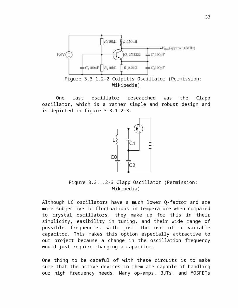
39
time, it’s about all that’s needed for most users of RC cars, and larger designs can be implemented as needs arise. Upon researching our options, we found a relatively inexpensive yet practical model. We need to design the capacitor array around 2 features: The capacitors must be able to provide enough energy, and they must provide enough voltage. If there isn’t enough energy, the car doesn’t run for a long period of time. If there isn’t enough voltage, the components/motors within the car will not work. We found 350F capacitors rated at 2.7V each made by Maxwell Technologies. Considering the car runs at 6V, we need to have at least that much voltage.
Because of the way capacitors behave, it’s better to beat this required run voltage by a fair margin, as the capacitors will lose voltage as their give off current. We decided to go with 3 of these capacitors in series, which will make an equivalent capacitor with a rating of roughly 117F and rated at 8.1V. Specifically, we went with the 350F model because it has a large amount of capacitance, but the 350F model is significantly cheaper than most other supercaps, even those with less capacitance than itself. The 350F model is also going to give us a lot of energy to use without taking up too much space like the ultracap models do. Some of the ultracaps are roughly as large as a 24 ounce aluminum beverage can, and some larger than that still. Putting something so large and weighty on the RC car will greatly increase the load and thus increase the current draw, so the larger size would negate any gains we had in energy storage. The Supercaps are only the size of a D-Cell battery each, so putting a few of them on an RC car isn’t an issue. Below is what these supercaps will look like and how large they are.
Figure 3.6.2 - A couple of 350F Supercaps from Maxwell Technologies
Given that the energy stored within a capacitor is calculated as 0.5*C*V^2, this array will contain roughly 3.8kJ. Applying a linear extrapolation of the energy value for our 15kJ battery would make us assume that our car will run for

40
between 7.5 and 10 minutes on just this array. However, because the car requires at least 6V to power its components, it will stop working shortly after the capacitor drops below this value, which means that the capacitor array will still have roughly 2.1kJ of energy left within it when the car shuts off, and that only 1.7kJ of energy will be dispersed to the car.
Applying the same extrapolation, we see that the car will only run for 3-4 minutes, assuming ideal conditions. In actuality, this value will be even less because the higher initial voltage will also mean a higher power consumption at first, since the car has a constant equivalent resistance, meaning it will consume even more current at first. To alleviate this, we will simply put 2 of these arrays in parallel. In doing so, we will effectively double the energy storage of the array without increasing its current draw. This should, therefore, allow the car to run for at least 5 minutes between charges, if not longer.
In the case that this array doesn’t provide sufficient run time, and to further maximize the potential of the capacitor array, we can implement a boost circuit that will allow the capacitors to draw energy at even lower voltages. If this design is used, we will also implement a voltage reference to ensure that the car is not being supplied with too much voltage or current, which would both damage the components within the car and draw too much energy from the capacitors.
Charge time is also still a concern. Despite the much quicker charge rate of the supercapacitors, there is still a certain amount of time necessary to charge them. This is further problematic when considered simultaneously with the limitations of our wireless power design. In our wireless transfer system, it will most likely only transfer between 30 and 50 watts to the capacitors, even after factoring in efficiency and loss.
The quicker charge rate of our capacitors also requires a larger power supply to give the amperage necessary to facilitate a significant reduction in charge time. Ideally, we’re going to shoot for at least 15V DC supply with 2A supply, assuming we will only have 30W to work with after the transfer. The higher voltage will allow for a much quicker charge time, but has to be employed carefully. If the capacitors are charged to too high a voltage, they will blow up, which would be disastrous considering their size. In the design section, we will discuss one such circuit design that we can make to use a higher voltage for quicker charging without any risk of causing a malfunction in the capacitors.
One of the major advantages to supercapacitors or any capacitor for that matter over standard batteries is their charge retention rate. Batteries are notorious for dissipating or entirely losing their charge value if left alone long enough. As a result, it can be problematic for people who have equipment requiring electrical current to operate that is left to sit for a long time. Many times leaving an emergency flashlight in storage for years will render them unusable until the batteries within them are changed out. High-storage capacitors on the other

41
hand, especially super- and ultracapacitors, dissipate their charge extremely slowly when compared to batteries.
They can be manufactured to have high parasitic, sometimes called leakage, resistance which is effectively a resistor in the 100M- to 1G-ohm range. This equivalent resistance is a series resistance the capacitor experiences when it is actually in open circuit, and the higher the value, the better the retention rate. There is also the Equivalent Series Resistance, which we want to be as low as possible to avoid any severe buildup of heat within the capacitor. The ESL we want to have as low as possible as well. Higher inductance will mean that the component is more resistance to step response, something we’ll encounter when turning the car on/off and when it begins charging. Ultimately, unless the ESL is some absurdly high value, it shouldn’t have a dramatic impact on our capacitor, since the capacitor is going to be used in a DC configuration.
Figure 3.6.3 - Equivalent Model for Standard Capacitors
Our main interest behind this type of project is the hopes of scaling this up to electric vehicles. There, weight and size won’t be nearly as much of an issue, and standard automotive capacitors show that the engineering community is on its way to getting capacitors with significantly higher energy density levels. The biggest problem facing electric cars today is their charge times. Standard home outlets require 5+ hours to charge a car enough to let it drive 200+ miles. Reaching this level of performance is still quite a while off, and would require roughly 2.5 mega farads to match that energy capacity, a difference of almost 1000 times what modern ultracapacitors can store. This number is made even larger when you consider that you would need 5 or more ultracaps in series to match the voltage of a standard car battery, which is 12V, effectively quintupling the required capacitance. Basically, it will be a long time before cars can be run on an ultracap array, but we can see from recent advances in capacitor technology that such a concept may be realized one day.

42
While not as ideal as never having to charge the car, it still forgoes the horrendous charge to run time ratio seen by most modern RC cars. As seen by our car, the charge time to run time of most batteries is as low as 5:1 and may be higher than 10:1 for more inefficient designs. The ratio for our system may be as low as 1:1 or as high as 2:1, a marked improvement, at the cost of having to charge more often. Plus there is no need to remove the battery manually and charge it. With this design, you can simply place the car on top of the wireless charging pad, or even drive it over the pad yourself.
Similarly, both capacitors and batteries themselves have an inherent internal resistance that they experience when put in series with a resistive load. This internal resistance causes a limitation on exactly how much current the capacitor is able to give off, and it is notoriously low for any capacitor, while it is much more noticeable for a battery. Because of this low ESR, capacitors, especially supercapacitors, can charge and discharge at a considerably higher rate as compared to batteries, and suffer less wear and tear from doing so, greatly extending their life expectancy. Modern capacitors placed within computers can last as long as 10 years. This also allows them to be charged and discharged many more times than even rechargeable battery cells. Such a property alone would justify paying more for capacitors versus buying new battery packs as needed.
The car will hopefully also have some other features implemented. We may or may not need a microcontroller for some of these. We are playing with the idea of using even higher voltages and having this microcontroller control several features. For example, we could have some kind of a digital potentiometer set to increase/decrease the resistance so that the car is only drawing 1A at a time, never anything higher. This would both prolong the run time of the car and reduce and damage to the motors from drawing too much current.
If this system becomes practical, we may be better off setting the capacitor array to even larger voltage values, which will allow for a significantly quicker charge time without risk of damaging the supercapacitors. Furthermore, we could use this same voltage monitoring technique to issue a warning when the supercapacitors are low on voltage, maybe through an LED. While a simple comparator circuit would accomplish this, if the microcontroller is being used anyway, it would just simplify the design process if we decide not to control this through a microcontroller.

43
3.7 Data AcquisitionInformation is vital to this project; not only preliminary research information, but information regarding periodic samples taken as the project runs. The data needed will be paramount for testing and operational effectiveness of this project as we determine the component level inputs and outputs, to system level efficiencies. In the following sections, the tools utilized to and reasons for data acquisition are explained.
The different layers of information that will be collected at specific points as testing for each level of the project is conducted serve to aid in determining the important values of this project, namely the efficiency of the inductor coils in the use of the wireless transference of power. To do so, voltage, and inductance values need to be monitored. This data must be gathered in parallel at the junctions that connect each of the vital systems which allow for the system to work as a whole. The vital junctions are those between the 60Hz AC to DC; DC to 10MHz AC; inductor resonance coupling efficiency; 10MHz AC to DC; DC to capacitor bank; and finally to load use.
This portion of the project will require a system of organizing and digitizing the information. At the beginning and end of the inductor coils and load of the project major subsystems, there are a voltage potential efficiency being taken periodically so to understand the gap required maintaining the right resonance coupling. Information will be gathered using a set of different sensors.
This data will be taken to data-compiler software which will catalogue the data for easy calculations which efficiency coefficients and power outputs can be calculated. This data in turn will feed a data processor to output digital variables on an embedded user interface. (See figure 1. Data collection and power flow)
3.7.1 Programmable Systems Other than a Microcontroller
In order to do this, a system of data collection is necessary. There are two primary methods of which to do this, the use of and FPGA or the use of a specialized microcontroller. The FPGA will be discussed first.
The FPGA holds the benefit of being very flexible in usage, encompassing any potential uses that can be thought of. The FPGA can be purposed to the customized needs of the user through the use of highly complex gate arrays which serve as programmable logic systems. Because of this very principle, an FPGA can be purposed as any multitude of microcontroller architectures or even microprocessor set up as well. It would be ideal if in an application of industry where a multiuse chip is a viable option for future repurposing to improve hardware efficiency.

44
A technology that has become available for testing purposes is the possibility of using a Digital Signal Processor (DSP). This became an option when Texas Instruments took lead of the industry and made mass producible DSP development boards and chips. Primarily, DSP boards are used for complex mathematical calculations (i.e. fast Fourier transformations, fast Fourier filters, or Laplace transformations) and image processing purposes. This is because the rate at which the DSP processes data at such a pace that information needs to enter and leave quickly. The DSP controller comes with the added benefit of being C-code compatible, making them remarkably easier to program then an FPGA which requires a hardware description language to design a code to form complex functionality. Despite this, digital signal processors are also compatible with the use of hardware description languages with data processing (again primarily for image or high volume information applications).
Like an FPGA, they can be purposed to many different functions and ramp up processing speeds dramatically. This means that sensor data would be accessed quickly and in large volumes. Of the data being able to be observed and processed, a very quick response to system changes as well as extremely accurate observations can be taken from the system with the use of the DSP chip. The necessity for such an up to date sampling is not exactly required for the scope of this project as well as for simple measurements being sampled are our primary input from this project, so it is not considered a primary choice for what the project requires.
For the scope of this project though, the interchangeability (of both FPGA and DSP chips) is unnecessary. The one potential downside to the use of an FPGA is that they are highly complex to code due to the use of these complicated gate systems. The practicality of using an FPGA is possible if given enough time, but to better use time, it may serve better to consider this a secondary option with too much coding expertise necessary to use it as a method of data collection when more practical options exist in the use of microprocessors. For the DSP chip, the programs required to program a digital signal processor are extremely expensive, typically ranging from hundreds to thousands of dollars which places it far from the reach of ordinary hobbyists or independent projects not connected to a large corporation with large coffered to dip into. However, a DSP addition to a microcontroller is a viable option to be able to calculate a frequency value to verify working of the oscillator circuit.
There are numerous companies to choose from for usage of the microcontroller part. Texas Instrument makes numerous models of processors from the MSP430 to the Stellaris ARM Cortex. Microchip is another processor designer with their many different PIC and dsPIC lines. Another company which notably designs microcontrollers for this purpose is those of Atmel and their AVR series. The last possibility is the microprocessor of Parallax with their Basic Stamp line of

45
products. To choose one of these would be best, the selection process will be discussed more in the Research section for Data Acquisition.
Figure 3.7.1-1. Data Collection and Power Flow

46
After this, the decision of how to transmit the data between the microcontroller (or data collector) to the computer where the data will be compiled must be decided, it can be hardwired or wireless. For ease of use, it will be hardwire, but if possible (for convenience sake) it can be wireless.
This will lead to the final decision of how this data will be translated into visual data by choosing the proper software to display the information collected by the microcontroller.
In the following section, the topic of microcontroller choice and justification shall be discussed. The three primary equipment requirements of this project are a microcontroller, sensors, and the analysis software. After, the ideas of how this will all be configured, and designed and coded will be discussed.
3.7.2 MicrocontrollersAside from being responsible for the purpose of collection of real time data, the microcontroller (unlike the FPGS (easily) and the DSP) is capable of controlling an analog output and input. In the instance of the project at hand, this means the microcontroller is also responsible for halting charge when the capacitor array is full, indicating low capacitor array voltage, monitor charge level of capacitor system, and coordinate with a smaller, wirelessly enabled smaller microcontroller to be able to speak and collect data to monitor the voltage levels of the capacitor array for safe application. To better understand what specific architecture to use with this project, a quick observation of the different primary architectures from which all architectures derive from.
3.7.2.1 The Basic Architectures:Before tackling the topic of which microcontroller to use, it is imperative to understand the architecture used by the microprocessors in question. It becomes important when understanding the microcontroller offerings in the next portions of the microcontroller decision.
The main reason for making this portion of the paper is to understand the different architectures and their benefits and downsides towards the project. The three main types of architectures that will be examined will be that of Von Neumann/Princeton Architecture, Harvard Architecture, and Modified Harvard Architecture.

47
3.7.2.1.1 Von Neumann Architecture:Von Neumann (also sometimes referred to as the Princeton Architecture) is one of the most hardware efficient style architectures used today on the market. Dating back to the 1940’s, it is also one of the oldest architectures still in regular use today. Von Neumann architectures have evolved from large rooms with large parts, to being as small as fitting an entire architecture that can be compiled onto a single chip. The primary outcome of this architecture is that it will remain simple with one dedicated set of stored-programming. Because of this, it is possible to reduce it to efficient hardware design to memory, processor, and an input and output device which can act like memory to function external input and output functions. This translates into lower power requirements for any architecture configured in this architecture. All data within this style are stored in read-write, random access memory. It was the first architecture to incorporate the concept of a universal coding concept that is applicable to all computing possibilities imaginable. It is the basis for what is to become low cost modular architecture which focuses on minimal hardware needs with complexity based in the software. This is a highly adaptable architecture for a microcontroller since it has such basic hardware needs. Cortex-M0 lines and MSP430 microcontroller’s architectures are notably Von Neumann. The one setback for this though is that it will not sample as quickly as the next architecture consideration.
3.7.2.1.2 Harvard Architecture:The Harvard Architecture is a more recent development than its simpler Princeton Architectural brother. An architecture which is marked by a clear distinction between storage and signal pathways, all of the data flow at one point rushes through a central processing unit or control unit acting as a midway between instruction memory, data memory, an arithmetic unit, and the input/output device. It is a more complex architecture compared to that of the Von Neumann architecture and because of so, it can act multiple operations at once. Hardware requirements for this though increase as the data paths are more intricate by two full separated systems as compared to the single data path for all functionalities of the Von Neumann architecture. For an example of this, it means that the Harvard architecture can read an instruction and access memory simultaneously. Complexity can also vary within the Harvard Architecture by being able to utilize different sized memory and instruction values for the purpose of making more efficient the coding with set known set sized values. COP8 is a microcontroller architecture primarily used by the products of national instruments which is influenced by the Harvard Architecture. The DSP chip model TM320 from Texas Instruments uses this hardware architecture as well to utilize in full the time efficiency of the architecture since bottlenecks are a non-issue thanks to the fully separated addresser and memory model. In microcontroller offerings, AVR from Atmel, PIC family of microcontrollers from Microchip, and Cortex-M3 from ARM utilize a Harvard Architecture.

48
3.7.2.1.3 Modified Harvard ArchitectureThis next architecture is an interesting architecture since it is not strictly a Harvard Architecture or a Princeton Architecture. In fact, it is viewed typically as a hybrid of both systems. By utilizing the same architecture as that of the Harvard Architecture, it can read and write to both instruction and memory similarly to that of the Princeton Architecture by using combinational Modified Harvard Architecture. By this idea, the architecture can benefit from both of their advantages with little addition to downside. It will be allowed similar speeds to that of the Harvard Architecture, but with the accessibility and memory/input-output addressing concept as that of the Von Neumann/Princeton Architecture which simplifies the data flow of the microcontroller or microprocessor. The data and instruction are still stored separately, but mapped differently with program-stored instructions typically taking precedence over data memory. The distinction between a Harvard Architecture and a Modified Harvard Architecture, and by use of some examples of purely Harvard Architecture, one can see what separates the original from the modified format of the Harvard Architecture of computer architectures.
3.7.2.1.4 Wrap up of relevance:By observation of the finer aspects of their respective build, we can see some examples as to why the PIC family of microcontrollers from Microchip, as well as the AVR family of microcontrollers by Atmel would be regarded as, clearly and distinctly, Harvard modeled machines because they do maintain a distinct and finite separation between instruction code addressing memory and data addressing spaces, and address 'zero' of each does, in fact, refer to a physically different piece of memory. However, the convention of considering them identifiably distinct is made opaque by the colloquial use of the term "modified Harvard architecture" to refer to such that work upon the idea of including special instructions to read and/or write the contents of code space as though it were data. It is this distinction that makes Modified Harvard different from the architectures spiritual parents of Princeton Architecture and Harvard Architecture. It is important to understand this distinction since (as stated earlier) that the AVR family and PIC family of microcontrollers are based upon this model of data processing.
What is important as well with specific architecture style is the size of the architecture. They are typically broken down to 3 primary sizes. 8-bit architectures are the simplest can easily store large instruction sets. A 16-bit architecture is useful in being of moderate size and not too burdensome to be too heavy for use with a small project. A 16-bit architecture in this consideration is probably one of the most useful aspects of this project as it is not too long to take up too much of the memory/input program space.

49
A 32-bit is likely the largest microcontroller on the market today. This would only needed if the requirements for the project are to reach into high amounts of calculation or numerous sets of complex and varying actions depending on memory or peripheral manipulations. Many of these microcontrollers which are of the 32-bit size use an ARM-based high-speed microprocessor. Beyond the standardized format by ARM, other companies like Atmel, Infineon and a host of other microcontroller providers provide other types of large instruction microcontrollers. One benefit of such a style of microcontroller is that it can allow for microcontrollers which could have integrated Digital Signal Processors. But this again, is the testament to the high data throughput required to make such large microcontroller use reasonable.
3.7.2.2 Microcontrollers:Microcontrollers maintain being a focal point with respect to the area of data collection and overall digital computation of a project, it functions as the brains of the operation, and directing data and action flow at near instantaneous to human speeds. What makes them integral to this project is that the microcontroller is an inclusive package for which data, sensor input, and visual outputs can be processed
They are a viable option now as opposed to years previous as of currently due primarily to economy of their use. They have reduced down to such simple hardware that many microcontrollers can now be packed onto a single embedded chip. What once took the machination of a room with complex and power needy equipment can now be found on the tip of one’s finger. The recent advances in flash memory has been a large player in this, as data can now be compiled onto a microchip rather than on bulky hard disc which require housing and moving parts. The advent of better technology on the nanoscale and architecture has led to them being available for use on this project. With build-up of their being economical, microcontrollers are now cheap and simple enough for hobbyist project use.
In addition to strides in cost effectiveness, steps have been made into making strides in accessibility of these products. The improvements in the design of development systems for have aided in support of the microcontroller of various designs and makers. TI with code composer and Microchip with MPLAB have allowed, for example, uniform systems in which entire families of microcontrollers can be programmed. This will be discussed more in the software design specifications.
Beyond this though, the architectures used by all microcontrollers have turned from proprietary systems to mostly open source programming which is a large benefit for the development community who strive to make their niche within their programming and project needs. To stream line this as well, an added benefit to

50
some of the newer software to program these microcontrollers, they come ready to be programmed in higher level code like C-code. With this, it is the result of easy access to help from fellow programming enthusiast on digitally heavy projects can be tackled more easily than in previous generations. With respect to this project, applications can be found for any of the microcontrollers that are on the market, only to find the right one will be the question.
The next section is one of the most important considerations with regards to the collection of data upon this project. It will limit the equipment types we can use and what language will be programed since each has their distinct assembly level language and syntax. Some peripheral uses with this project using the microcontroller are displaying data, frequency calculation, and managing manual adjustments.
The reason a microcontroller instead of a regular computer is the fact that the microcontroller itself is relatively very low power needs, meaning that use of these will have minimal impact on the working of this project.
It is best to discuss all possibilities of microcontroller possibilities. As will be stated in the Design phase of this report, to see a few of the primary competitors for the process of selecting a microcontroller for data acquisition are those of Texas Instruments, Microchip, Atmel, Infineon, NXP, and Parallax and their respective chip and processor architectures. In this section, we shall discuss the process the positives and negatives of each with respect for this project broken down into models
3.7.2.2.1 Texas instruments:On Texas Instruments, they are the most prospective company to work with on regards to the semiconductor technology to use, as their technology is what is taught in embedded systems. On top of that as well, the work of coding the microprocessor can also be done in C++ with their MSP430 series of embedded microcontroller. The company’s two main offerings on this project would be their MSP430 and Stellaris lines.
It is best to focus on MSP430, though, since it is their primary contender for the position of low powered microcontroller. The MSP430 family of microcontrollers utilizes the Von Neumann Architecture with a 16-bit instruction size to keep the power requirements and hardware requirements of the microcontroller low. This though is at the sacrifice of slower data flow from shared data and program memory buses. There are many variations on the MSP430 family as each suit more specifically the needs of the customer. To single out one specific type, one needs to understand the design first. This will also be the similar concept that will pertain to all other pursuits with searching for the proper microcontroller from each company.

51
A second offering from Texas Instruments is their line of digital signal processors (DSP). As recent years, Texas Instruments has pioneered the commercialization of this technology. One potential product that Texas Instruments provides to fit our needs is their TMS320 line of DSP boards. The benefit of this technology is that they can process information quickly due to the data being analyzed in digital format from analogue and then summarily retranslated into an analog signal. They can as well sample at extremely fast rates than typical microcontrollers. This is due to their need for the processing style requiring large amounts of data in order to operate to the technologies fullest potential. An older, but similar technology that TI offers which could be used as a DSP is their aging OMAP chip set for multimedia. Since this project does not encompass that, it is not a good fit for this project right off the bat.
Both of Texas Instruments DSP and MSP430 are compatible with the C-programming language, which is an added benefit of the use of their products.An added benefit to the DSP chip though is the potential use of hardware languages as well as C languages to improve the functionality of the processor. But, a monetary issue arises though when the microcontroller exceeds 16Kb of programming and the use of DSP programming. They would require software costs ranging from a few hundred to a few thousand dollars in order to program and compile using these chip sets. Their baseline program Code Composer is complimentary up to the 16Kb size code.
TI overall though, does not sport as large overall community support as compared to their two rivals. Also, unlike their primary rivals, TI offers a large incentive to use and market their products by using them in one’s project by offering a contest and a possible grant in parts for an arranged price ceiling. Their technology as well sports the lowest energy requirements of their field.
3.7.2.2.2 Microchip:On Microchip, it had accrued a strong user base with large community support for projects and development. Their primary offering as a company is that of the 8-bit and 16-bit PIC microcontroller or their dsPIC microcontrollers. Because of the strong offerings of the PIC community, they can provide a good template to streamline the design and prototyping process of the project as well as host many current enthusiasts whom are highly knowledgeable in the application of their chipsets.
To program Microchips, they host the MPLAB line of compiler software. This software is the universal basis for coding on any of their chips from PIC to their dsPIC lines as well as their PIC32 MCU (which is not a microcontroller). The program offering are its free, standard and pro editions which primarily very by the optimization levels as well as the complexity of which the user can pack more

52
operations onto the chip as any given time. For the use of this project, such compactness is not necessary, as baseline specifications will only require the most basic functionalities of the microcontroller.
Their products boast we well the possibility of using graphical displays for ease of use as well as access the majority of interfacing methods. Sensor equipment should be compatible with the use of this family of chips as well.
The primary selling point of this line of product is the fact that they offer a long line of experience in the field of college project style programming and microcontroller experience. With respect to Microchip’s history, their PIC or dsPIC lines of microcontrollers prove to be a strong contender for data collection and manipulation.
The PIC family of chips primarily hosts cost effectiveness, energy efficiency, and reliable performance with which it all comes packaged in a system which is at the most important level, a highly flexible system which will allow easy integration into many different projects.
DsPIC controllers are a derivative of Microchip’s PIC controllers. They combine the use of a microcontroller and digital signal processor for the combined use of fast pace processing power of a DSP with the architecture of a microcontroller. These, though, are ideal for the processing of advanced data heavy applications like image or audio processing algorithms.
3.7.2.2.2.3 Atmel:On Atmel, again like Microchip, they host a strong user base and can fill many roles of providing a good template to streamline the design and prototyping process of building this project up from the ground up. Their primary draw though is that they claim high flexibility in scalability as well as an exceptionally strong community which to troubleshoot a problem when need be.
Atmel offers four different types of microcontrollers; the AVR line, ARM derivatives, MCU wireless, and 8051 architectures.
Of these, AVR is probably the most likely candidate for use of microcontroller since it boasts 8-bit and 32-bit variations as they are designed with economy and ergonomics in mind. The family of chips can be coded in either C or assembly languages and boasts performance levels at very cost effective levels including being highly energy efficient. This family of chips will be discussed more later on in the design portion of the data acquisition. Though this family does carry many variations of a similar architecture, what is important is that there is a large support base for this line of product.

53
Another line of Atmel chip are their ARM derived controllers. These are ARM style chips, native to the 32-bit processing memory size, are the primary choice for applications requiring high rates of cycling, for example, in instances of image and audio processing. The chip family itself can handle enormous amounts of data for being a microcontroller possibility, but it is not a microcontroller by its nature. It is primarily a microprocessor which can perform as a very low power computer chip. The chip can be configured to work like a microcontroller if given the proper hardware to do so. But, like the DSP and FPGA chips, the complexity of this architecture of chip is not necessary (if not overkill) for the scope of this project.
Next is the wireless microcontroller unit. In this package, the primary size for the consideration of the consumer is the 8-bit single-chip microcontroller. All packages of the wireless communications concept would be aided by the fact of their performance are intertwined. If larger microcontroller architectures were to be pursued, a 32-bit AVR or ARM architecture would be compatible with an external transceiver unit attached as a wireless communications peripheral. In this class of microcontroller, this holds an advantage in the field of microcontrollers by being a set which is guaranteed viable as an option for the applications of wireless connectivity with the car (load) in the later portion of this project where wireless communications is a necessity to be able to sense in real-time the power usage of the system.
Atmel prides itself with the experience it has in the field of the utilization of Intel’s 8051 architecture. Being consistently an 8-bit microcontroller architecture that utilizes the Harvard Architecture, it has the guarantee of being able to be space efficient with its program code since it uses a tried and true instruction set. Included is the fact that Atmel also hosts a very strong support for project development with this microcontroller since it has been under use for an exhaustive history of project usage.
As a side note, Atmel products are the controllers used Arduino prototyping platforms which have been popular within the last years with hobbyists which can be hand built or pre-assembled.
The next two companies’ products are typically aimed towards industrial applications and use in many different fields of which small efficient computers are needed to digitally control and direct logic systems to automated functions. Infineon and NXP are well known in their respective fields of application from the medical industry to the automotive industry.

54
3.7.2.2.4 Infineon:Infineon is a company which focuses primarily on industrial applications by use of the automotive industries microcontroller needs in the ever digitizing car equipment. Their highest offering thus far is microcontrollers built around a 32-bit ARM or Infineon’s TriCore architecture. With smaller architectures, Infineon designed the 16-bit C166 architecture which improved upon their previous chip offering based on the 8051 Intel Architecture.
The 32-bit ARM architectures break down into two specific types, the XMC1000 and XMC4000, with the 1000 series intended for motor control, display interfacing, power conversion, as well as being a general workhorse. The 4000 series though is an upgrade from its predecessor as an industrial controller for the same uses as the XMC1000 including heavier duty responsibilities like Input/outputting, power inversion, and generally heavier processing purposes. Due to their product being for industrial purposes though, their ARM series of products may be too over-powered as well as being costly for its industrial certification.
The 32-bit TriCore is an original design by Infineon as a 32-bit RISC microcontroller with DSP capabilities integrated into a single chip. It would come with special software which improved the safe operation of the hardware. It was originally designed with a safe, reliable and efficient controller which is specific to the automotive applications. For this, it is not a primary consideration of microcontroller architecture choice. It is worth noting though it is possible to use and understand better as the architecture holds promise for large scale use in its target industry.
C166 architecture came from when the company was owned by its parent company, Siemens Semiconductor Division. For their size, it is quicker than the 32-bit architectures in some models due to its low-latency design. But, they are intended for industrial, automotive, and communications applications, not exactly the target for this project. It is worth looking into so one can better understand the flexibility and intended use of all architectures for the best fit.
Like other 8051 Architectures, Infineon’s 8051 chip are designed into the XC800 Family of Microcontrollers. This is further broken into two different applications, automotive and industrial. Automotive models can be used in motorcycle sensors, automotive throttle controls, window motors, and simple applications within car systems. Industrial models can be found in air conditioners, digitally controlled power supplies, and basic motor controls. Again this family of chips is not exactly intended for our use. Infineon can be determined as most likely not a good fit for use on this project with collecting sensor data.
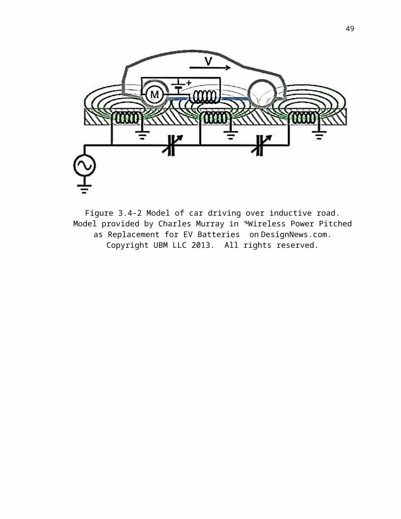
55
3.7.2.2.5 NXPNXP provides microcontrollers from the standard 8-bit to 32-bit instruction sizes, as well as a series of wireless microcontrollers. The 32-bit architectures range from the ARM7 to ARM9, and a various set Cortex series architectures. Both ARM (number) and Cortex are derived from arm architectures, but are not distinctly the same except for their instruction sizes and their use of RISC architectures.
Like previous competitors with similar hardware, their 32-bit hardware range specifications can be similar, varying only in essence on built in functions, the Cortex series being a prime example of this. Each type model available has different points depending on consumer cost and built in functionality. Like other higher levels of the 32-bit processors, they can boast built in DSP and low-power A to D or D to A devices. NXP prides its technology on their legacy of being a workhorse of the semiconductor industry. To hobbyist, they are not the most new user friendly but still a worthwhile company to work with as many other possibilities lay for the career digital-tinkering junkie. Their main draw for their technology comes from consumer dependence of those who are already accustomed to their technology. But other than so, they are very similar to other competitors in the field with regards to the 32-bit microcontroller market and their ability to place integrated features into their technology. What is noteworthy though is that NXP’s wireless microcontroller designs are only capable within the confines of 32-bit architectures and nothing smaller. This may be too large for the needs of this project, but it can be utilized if necessary but with an increased hardware waste. What is needed is the fact that it be a wireless microcontroller. So that places the JN5164 as a possibility for use. (To be better discussed in this design requirements)
As for NXP’s offering for 8-bit architectures are based upon the 80c51 family of microcontrollers, proprietary to Philips technology. This architecture as it holds 4k of 8-bit ROM with 128b 8b RAM with a limit of 4 8-bit Input and output ports. Like other architectures, it does have capabilities of utilizing UART and additional clocks or power down interrupts which can halt the clock without disturbing the RAM. It is a tried and tested architecture based on the Harvard Architecture which makes it terrific for multitasking purposes.
At the 16-bit level, NXP offers the XA core microcontrollers which are touted for being good for industrial applications. There are three variations on the XA’s with the XA-H3, XA-H4, and XA-C3 with each touting specific variations. For example, the XA-H4 is an enhanced version of XA-H3 with added DRAM, Von Neumann Architecture, Harvard Architecture, and USART supports. XA-C3 are for more communications uses with the feature of easy 8-bit architecture compatibility for ease of upgrading from an 8051 architecture.
56
3.7.2.2.6 ParallaxThe primary offering of the Parallax Company are their line of Propeller and BASIC Stamp boards. These products are usually tools designed for beginning hobbyists and college freshmen new to robotics.
The Propeller chip is fairly basic, providing only one style of chip that utilizes a 32-bit command. It is an all-inclusive chip which can operate both high-level and low-level commands via and on-board interpreter. On top of this, there are many standardized codes which are allowed with this product. Like the other providers, they sport a multitude of peripheral applications. What is not included though is with their BASIC Microcontroller line, is compatibility with the C-programming language translator and must therefore be programmed strictly in BASIC. Their propeller line of microcontroller though requires a bit more application of higher level digital skill; although, like the BASIC, their products still maintain a high level of simplicity.
On Parallax, they provide highly elementary and simple to use equipment, but compared to those of msp430 or any of their competitors, it is exceptionally pricey. On top of these, parallax is primarily directed toward basic uses, educational purposes and a younger audience composed of beginner students. Because of this, their products are not exactly designed with building the basics in electronics understanding since the components Parallax sell are mostly pre-assembled and only require basic assembly skills of the larger components. Their equipment can fulfill the functionality required, but, their technology will not fulfill the design requirements of this project.
3.7.3 Peripherals/Sensors/Displays/Communications equipment
A microcontroller is important for a project because it is able to process many different functions. In this case, the main use is to control and manage peripherals, like an individual’s brain would control their limbs and mental processes. In the case of a microcontroller, the applications are those of peripherals able to do what the microcontroller cannot inherently. The functions this microcontroller will need to do are maintain wireless connections, observe voltage inputs, control charging, observe load discharge, regulate discharge and output a visual display of what relevant values are, be they numerical or graphical, depending on the user’s needs. This section will tackle what sensors and peripherals are needed to complete the necessities of this project.
3.7.3.1 Wireless communicationFor the application of some sets of sensors, there needs to be wireless access, primarily within two legs of the system which consist of between the receiving

57
inductor plate and the DC converter; and a sensor right before and after the capacitor array. This is important for the accurate observation and tuning of the inductor coupling system as well as to monitor if the capacitor protection circuit kicked in or not. For this, wireless capability built into the microcontroller could be used for our purposes as a peripheral feature. As for the actuating of the inductor plates spacing, this will be done manually for ease of application. If time permits, digital actuation can be added in as a feature. But, alternatives do exist.
This can be done using products like Bluetooth, Zigbee, or other IEEE 802.15.4 approved designs. To explain, IEEE 802.15. a standard for wireless communications community to design around which is the basis for Zigbee, MiWi, and ISA 100.11a. It offers an available standard which allows for unique ease of use in airwaves that are usually regulated by international bodies. The Zigbee configuration of communications protocol and hardware is most likely what will be used with this project since they have proved to be field reliable for specific microcontroller architectures and peripheral devices. It is the choice for small projects for its low cost and low power features. It is ideal for the needs of a wireless communications device as simple as what the project needs. As for hardware that Xbee’s are a possibility for application of a dedicated wireless microcontroller with good data feed rates. It benefits from the use of Zigbee’s standardized protocols with the ease of a simple plug and play style antenna system which is compatible as a small computer in its own right. It will require small programming, but should be able to fit the intended use for this project as a wireless device to connect a small array of sensors. It is a major contester for the spot of fulfilling the wireless needs of the project.
As stated just now, the alternative to a wireless microcontroller is a small microprocessor specifically for wireless communication with easy integration to a larger project. The alternative is an integrated wireless microcontroller which is restricted to smaller a instruction set and less hardware specifications on many wireless microcontrollers which are intended for use as a wireless microcontroller.
3.7.3.2 Voltage sensingVoltage sensors will be needed at each transition point to be able to monitor issues as they arise and to be able to effectively tune the inductor system. An analog to digital converter can be used directly from the line in order to determine the voltage level at the node of interest. The principle of which the A/D converter is to translate an analog signal (in this case) voltage into an equivalent digital numeric value. Important aspects a converter will be its resolution and physical tolerances which will dictate the bit size of the AD Converter and cost of part depending on how costly more stress tolerant materials are. Since this is a straight conversion, it should be a simple design. This technique would only be applicable for DC .

58
3.7.3.2.1 High voltage issue:These ADC will be needed as a mid-step in case of mistakes so if the ADC fails, it will not destroy the microcontroller. The explanation for this redundancy is that there are high voltages being examined at all steps of this project. So in the design portion this issue will be tackled, but to explain here, the relevancy looking to dealing with the problem is pointed out.
3.7.3.2.2 Observing Voltage Input:Through an analog to digital converter, data collected will be done at the AC to inductor juncture in order to have a base input voltage from the inductor system. A remote value will then be observed from the other side of the inductor system as an output inductor system to be able to calculate an efficiency value which will help in finding the maximum coupling of the system. It will be manually tuned by use of a screw knob that manipulates the level of the stationary inductor plate.
3.7.3.2.3 Observing Load Discharge Similar to the remote sensor for the end of the inductor system, another sensor will be connected to the output side of the capacitor array. The purpose of this is to be able to dictate logically the output of the potentiometer directly precisely and without human interaction necessary. This again will require an analog to digital converter that will read into comparison logic of the microcontroller which will alternate the resistance of the potentiometer to regulate the discharge of the capacitor array.
3.7.3.3 Regulating output:Potentiometers will play an important role in this project for they are important for this project to aid in regulation of the output of the capacitor array as well as potentially providing a solution for cutting off the charging process when the capacitors become full. The digitally controlled variant of the potentiometer will be the most defining feature of the load output system which will be monitored under the microcontroller to maintain a stable 1-1.2A output with a stable voltage so the super-capacitor array is drained at a constant discharge that allows for maximum time efficiency with the charge since the capacitor array cannot control its own discharge rate like a battery array.

59
3.7.3.4 Graphical User Interface:LCD Screen will most likely be integrated into the microcontroller board for simplicities sake. The type of LCD used will be dependent upon the company used. For example, an MSP430, AVR, or PIC may use a monochromatic LCD. Depending on complexity, a Color display can be used in this application of this project, but since user interface does not need to be exactly the most aesthetically pleasing for the scope of this project, a monochromatic display for voltage observation will be enough for this project.
These screens could also be fully colored as well, but the code implementation for one is more complex and much more sensitive hardware wise and software wise in order to be able to reach the ability of implementing one. Although, the added benefit of being more aesthetically pleasing does exist because of it as well as more potential functionality is possible as the screen limitations are significantly less with a color screen. It must be maintained though that the primary focus of the project is to keep things minimalistic to cut cost and headache down.
On more advanced boards, these can be built onto the microcontroller boards a prototyping board accessory to help make prototyping easier. The LCD can also be purchased as a separate component to complement the board in use, depending on the screens compatibility with the microcontroller.
3.7.3.5 Programming the Microcontroller:Some microcontrollers utilize a separate compiling hardware to communicate from a typical computer’s operating system to the microcontroller. Each model of hardware comes with a specific style of programming hardware; some are prebuilt, others can be built. What is important about this additional hardware is that they can implement debugging and make specific the read in instructions to that microcontroller. Connectivity is variable from a USB, rs-232 socket, or customized pin input. The additional hardware is quintessentially a debugger.
In the case of some of the MSP430 Launchpad or some similarly simple style of microprocessor, additional hardware is not necessary for the implementation of the microcontroller from the PC to the microcontroller.
3.7.4 Data Acquisition Software and LanguageWhat is important to utilizing this equipment is most importantly, what program is compatible to allow the ability to program the microcontroller. Now, there are many different languages to code in; MIPS, C, C++, C#, MSP430, BASIC, etc.

60
For this instance, it is important to realize that each company comes with their special language to code in. Much architecture are capable of being programmed in C and not require specialized languages, so being able to choose one which does work off of higher level languages is a benefit. There also are programs which exist that can code for many different microcontrollers since many of these microcontrollers are open-sourced, which then allows for libraries which are capable of housing many different basis and architecture programming parameters.
One important factor is the uniformity to operating system compatibility. Since the majority of programs which will need to be programmable in C, the programs should thusly be able to be useable from the Windows operating system. Those in the group traditionally use Windows operating system and for this project will continue to do so.
3.7.4.1 Programming the MicrocontrollerMany of the architectures with the 32-bit size instructions will be applicable with the MIPS language, so it is advisable to use this language as choice for this project if the C-language is not available for compilation on the board.
There is on the other hand, a program which is free and highly integrate able with 32-bit ARM Architectures which are popular on microcontrollers. Coocox CoIDE is a type of free open software which is used for advanced software development environments. In this case, it is a general purpose program to design instruction sets for the ARM Cortex Architecture. It is possible to use on products from companies like Atmel, NXP, and Texas Instruments (to list those embedded hardware companies analyzed in this research). The only requirement is that a specific debugging adapter is necessary to aid in the use of this software.
It will most likely be the best choice to use the software designed specifically for the microcontroller that will be used. Fortunately for the user, Microchip with MPLAB or MPIDE, and Atmel with AVR Studios provide their basic programming software for free, and similarly with Texas Instruments but to a lesser extent with their Code Composer with a limit of 16 kByte programming size for its complimentary variation.
3.7.4.2 Other Software:For the intention of this project as well as many others, PCB design software will be necessary to complete the senior design project criterion. One of the most important basic skills of an electrical engineer is the ability to design, map and order a Printed Circuit Board (PCB). One very popular program on the market

61
today is EAGLE. Potential second software to potentially be used is called Fritzing.
EAGLE, itself is one of the premier programs to design out a PCB. In use for over 20-years, the company and its employ know exactly what to do when it comes down to producing affordable PCB’s and thereby pass the savings down to the customer. The company offers its Cad-software free up to specific sizes and serves as a great learning tool as to understand how design of a PCB goes as well as offer a good customer support base for the engineer in training. This program will be important for all aspects of this project; from power system, oscillator circuit, inductor coil system, digital controlling, sensor stability, capacitor stability, and housing the microcontroller circuitry.
Fritzing is an open-source program that operates very similarly to that of EAGLE. Slowly they support for a program like this is growing as the need for designing more and more open-sourced software grows. Compatible with all platforms of operating system used today, it would be useful to learn. Though, it will lack in depth of use as compared to its well established rival. Fortunately, with Fritzing, there are many preset PCB designs available already, which make this a good candidate for a PCB cad-software.
4. Design
4.1 Design Power Supply
4.1.1 SpecificationsWhen designing the power supply from 120V 60 Hz AC to a pure DC voltage, consideration must be taken when having to meet specific requirements. For our project, the specifications and requirements are as follows:
Converting a purely AC signal to a strong reliable DC signal. Stepping down the AC voltage level to a feasible and workable voltage in
specification range (further discussed….) Generating a pure DC signal with enough voltage and power output to be
fed to further components with heavy consideration of future component specification, requirements and design.
Minimal voltage loss after step down and before load output. Keep Ripple Voltage or considerably noticeable and problematic “noise” to
a minimum in which can cause a substantial amount of noise during amplification stage of the design.
Maintain an efficient amount of power dissipation across component with both safety and accuracy.

62
Consider the operating frequency at the point in time where this component is being used.
Insure that the components chosen will be operating as expected from the operating frequency determined in the previous step
4.1.2 DesignThe following will be the more focused on the specific components and topology our low frequency AC/DC Converter foundation.
Simple enough our source of power will be a wall outlet of 120V RMS 60 Hz. This is practical to our application because if commercialization became a consideration, very little if not any change must be made to the components.
To begin the foundation of the design, we have first decided to implement the 5:1 Step down Transformer to obtain approximately a 33V output to transfer to the output of the AC/DC converter. This value is above the exact voltage we want because the rectification components and effective series impedance will cause enough voltage loss to obtain an output between 24-28 volts. The output value will also be overshot (only of a factor of 10-12%) to accommodate for future compensation of tolerance percentages in upcoming components.
After considering the topologies, the MOSFET Bridge in and H-Bridge configuration will best suit our requirements as described in section 3.2.2.3. As opposed to the well know Diode Bridge configuration, this will allow for higher currents draw and obtain a steady DC power signal with minimal noise, overall power dissipation conservation, and precision accuracy.
The component we have chosen for our rectification process will be the CSD18532Q5B and its opposing CSD25211W1015 Power MOSFETs. These MOSFETs has many built in capabilities that diodes alone do not have. It has a forward Voltage Threshold (Turn on) of +/- 1V; this may seem a little more than a simple diode but in when using the MOSFET Bridge described in section 3.2.2.3, as you can see the gate is connected in parallel with the MOSTFET such that no voltage drop will occur to the component on. In doing this the Drain to Source voltage will be determined by the applied voltage from the 5:1 transformer. Moreover, using these as opposed to power diodes because of the on current impedance in the range of milliohms will account for the amount of heat dissipation in the circuit. The Power Diodes will dissipate a lot more heat than the MOSFET and will eliminate the use of a heat sink in turn making our design more economical and more cost effective. In addition, the reverse recovery time for the MOSFET will slightly beat out the reverse recovery time of the diode. As the temperature increases in the diode so does the reverse recovery time. Instead, the MOSFETS reverse recovery time will insignificantly increase with
63
temperature. Lastly, it’s built in protection characteristics will provide us with voltage spikes due to its very high reverse current spike capabilities.
Smoothing capacitances and load resistances will be within the micro Farads and below the 1000’s of ohms range respectively. The values must be determined in a lab environment as simulation will not allow capacitances and resistances of different materials and their effective tolerance percentages. These basic components will be tested and exact values will be obtained through the use of a Digital Multi Meter.
4.1.3 SchematicsThe Schematic given below is the MOSFET Bridge. Simple Zener Diodes are used to keep the Gate to Source Voltage constant without overloading it (Zener diode voltages will be interchangeable to reflect necessary voltage push or pull for final output precision). The resistances shown are the equivalent resistances of the Power MOSFETS themselves.
Figure 4.1.3-1: MOSFET Bridge Rectifier in H-Bridge Configuration
4.1.4 ComponentsThe parts listed here are the components that will be used
Power MOSFETS (N Channel and P Channel Respectively)

64
Figure 4.1.4 – 1 CSD18532Q5B (Courtesy and Copyrights of Texas Instruments)

65
Figure 4.1.4 – 2 CSD25211W1015(Courtesy and Copyrights of Texas Instruments)
4.2 RF Power SignalIn the following sections I will be discussing the specifications and requirements, various available and pertinent components, and final designs and considerations for the programmable oscillator, class E power amplifier, and the gate driver, which all make up the generation of the high frequency power signal used to drive the transmission and receiver coils in the wireless power transfer.
4.2.1 Programmable OscillatorThe design of the programmable oscillator involves determining the necessary specifications and requirements, finding which available programmable oscillators meet those specifications and requirements, and determining which one is best for our project.
4.2.1.1 SpecificationsFor our project, considering what frequencies we would like to operate at, the class E amplifier we will be using to power the signal, and the use of a gate driver to power the transistor in the class E amplifier, the specifications, requirements, and considerations, in order of importance are shown below.

66
Can generate signals from 1MHz to 20MHz Good documentation to make utilizing it easier Availability Made by Texas Instruments in order to use credit from their senior design
competition to pay for it. Frequency step size: the smaller the better Price Low input signal current to not wear on the microcontroller too much Uses common rails such as 3.3V or 5V
4.2.1.2 ComponentsSadly, there were no Texas Instruments programmable oscillators that would have matched our necessary specifications. It seems most programmable oscillators that are readily available to small consumers are produced by Maxim Integrated. They have a wide range of programmable oscillators, most of which fall into our needs. However, I have narrowed the choice down to 1, the DS1077. This is the only chip that was readily available to purchase that allowed on the fly, in circuit frequency changing, which is what we are after with this part.
DS1077
Price $2.95
Frequency Range 16kHz - 133MHz
Supply Voltage 5 v
Supply Current 50 mA
Standby Current 2 uA
Power-Up Time 0.1 mS
Load Capacitance 15 pF
Operating Temperature Range negative 45 to 80 degrees C
Package 118mil μSOP
Number of Writes 10,000 minimum
Figure 4.2.1.2-1 DS1077 Programmable Oscillator Specs

67
4.2.1.3 ConclusionI was quite disappointed in the lack of readily available on-the-fly, in circuit programmable oscillators, but thankful that there is one that performs perfect for our application and is quite cheap. One thing to note, however, is that the DS1077 utilizes EEPROM to store its operation frequency. EEPROM can only be written so many times, so once our project is assembled and we have tuned the transmission and receiver resonators to their highest efficiency, we must be careful not to continue to arbitrarily write codes to the DS1077, as the EEPROM will eventually fail after excessive use. The datasheet did indicate that the minimum number of writes was 10,000, which should be plenty for our project.
4.2.2 Class E AmplifierIn section 4.2.2 we will be discussing the desired specifications and requirements of the class E power amplifier we will be designing, the designing of the various components, the schematics and relevant simulations showing the proper operation of the class E power amplifier, the choice of components to satisfy the schematics and simulations, and then conclude our final designs for the class E power amplifier.
4.2.2.1 SpecificationsIn accordance with the projects demonstration of charging an RC car with super capacitors instead of a standard RC car battery, we want to charge the car as quickly as feasibly possible. With that in mind, the class E power amplifier specifications, requirements, and considerations, in order of importance, are shown below.
Generate at least 30 Watts of power at 20 Volts, therefore we are transmitting at least an amp of current, which will increase the flux between the resonators, which will help the magnetic coupling.
Be capable of effectively amplifying a range of frequencies from 1MHz to 20MHz.
At least 70% efficiency Consider heat dissipation options
4.2.2.2 DesignIn order to design the class E amplifier for our project, we must determine which transistor will best be suited for our needs, what voltage we need to supply the

68
transistor with, and the output resonant circuit component values in order to resonate within our desired frequency range.A wonderful paper written by Nathan and Alan Sokal in the IEEE Journal of Solid-State Circuits details the equations used to develop the component values for a given class E amplifier specification (Sokal, 7); those equations are given below in figure 4.2.2.2-1.
Figure 4.2.2.2-1 Class E Amplifier Component Equations
Using Matlab with the given inputs, I determined R, L2, C1, and C2; the results can be found in figure 4.2.2.2-2.
Figure 4.2.2.2-2 Class E Amplifier Component Values
With these component values, we can develop our output RLC tank circuit for the class E operation of the amplifier.
For our transistor chosen in section 4.2.2.4.1, I have determined that a Vcc voltage of 30V would be optimal for our design. This would develop plenty of power and current at the output to drive our resonators.
For our Q value we referenced Sokal (Sokal 7) again in order to understand the tradeoffs between raising or lowering the Q value; we had to determine whether we wanted our amplifier to have a high efficiency, which means having a lower Q value, or having a lower harmonic content of the signal delivered to the output, which occurs when Q is higher. We chose a relatively low value of Q, 6, because the operation of magnetically coupled resonators is not immensely tied to the

69
precision of the signal, and therefore efficiency is of a much higher value to us than harmonic distortion.
The L1 in our design is an RF choke used to block high frequency currents coming from the power supply. In order for the RF choke to operate at our frequencies, it needs to be at a value of 50uH, and be a ferrite core. The ferrite core is advantageous to an open air core because the capacitance is much less, meaning that the self-resonance is much higher, and therefore better suited as an RF choke. We also need to be careful for the current saturation of the RF choke.
4.2.2.3 SchematicsFor basic schematic and initial simulation testing, I used multisim to implement a class E amplifier with the component values designed in section 4.2.2.2. Sadly, I could not find a method to simulate the gate driver and programmable oscillator in multisim, so I just used a function generator. The schematic for the designed class E amplifier is shown in figure 4.2.2.3-1, the output and input waveform simulation is shown in figure 4.2.2.3-2, and the wattmeter output is shown in figure 4.2.2.3-3.
Figure 4.2.2.3-1 Designed Class E Amplifier in Multisim

70
Figure 4.2.2.3-2 Oscilliscope Output from Class E Multisim Simulation
Figure 4.2.2.3-3 Wattmeter Power Output from Class E Multisim Simulation
The transistor chosen for this simulation can be found in section 4.2.2.4.1. This simulation verifies the initial designs for the class E amplifier needed to power our wireless power transfer resonators.

71
4.2.2.4 Components
4.2.2.4.1 TransistorFor the transistor in this design, special considerations need to be made. The transistor must be able to switch fast enough in order for the class E amplifier to effectively operate at frequencies up to 20MHz. The transistor must also be able to draw enough current at a voltage high enough to satisfy our requirement for at least 30 Watts to be generated for the resonant coils.
One transistor researched that can fill this roll is the LET20030C from STMicroelectronics. The relevant specifications for this transistor can be found in figure 4.2.2.4.1-1.
Another interesting FET that I stumbled upon that looks extremely promising for our project is the high-efficiency enhanced mode GaN FET. The eGaN FET is produced by Efficient Power Conversion, and has a really fantastic profile for our project. One interesting benefit of eGaN FETs over traditional silicon power MOSFETs is that they have a reduced Rds(on) and gate capacitance. Generally if we wanted to be able to switch a silicon power MOSFET faster, we would have to decrease the gate capacitance, but then that would lead to an increase in the Rds(on). The eGaN FETs have a significantly lower Rds(on) and gate capacitance when compared to a traditional silicon power MOSFET. You will find a comparison between 2 plausible eGaN FETs for our design in figure 4.2.2.4.1-1
LET20030C
Price $83.20
Max Vds 80 V
Max Vgs 15 V
Max Id 9 A
Max Power Dissipation 108 W
Max Frequency 2 GHz
Igss 1 uA
Ciss 58 pF
Coss 29 pF
Crss 0.8 pF
Figure 4.2.2.4.1-1 LET20030C Specifications

72
EPC1014 EPC2012
Price $2.70 $2.98
Max Vds 40 200 V
Max Vgs 6 6 V
Max Id 10 3 A
Igss 0.4 0.1 mA
Ciss 280 128 pF
Coss 115 73 pF
Crss 15 3.3 pF
On Resistance 16 100 mOhm
Figure 4.2.2.4.1-2 eGaN FET Specifications
Upon comparing the 3 transistors researched in this section, I have determined that the EPC2012 is the best transistor for our application. The LET20030C had a lot of very desirable specifications, but its price compared to the other two eGaN FETs made it completely undesirable. The eGaN FETs also have a much smaller on resistance, and therefore have a higher efficiency and produce less heat. They are also a much small size, making implementing the class E amplifier much easier on a smaller, and therefore cheaper PCB board. Out of the 2 eGaN FETs, the EPC2012’s much lower gate current and gate capacitances out-weighs the EPC1014’s higher Id current. For our design the EPC2012’s current is plenty, so it was an easy decision to finally go with the EPC2012.
4.2.2.4.2 InductorsUpon researching what inductor we needed to use for the output RLC tank circuit of the class E amplifier, I made sure to filter out any inductors that couldn't handle the currents that we will be involved with, that is, any below 5A. I don't believe we will be getting close to 5A, but it's better to be safe than sorry, plus the price difference is negligible.
From there, I had to determine whether we wanted shielded or unshielded, the tolerance, and the price. I determined that shielded would be the best for our

73
application because our transmitting resonator is essentially an inductor, and it would be best to minimize any cross coupling between the resonator and the inductors in the class E amplifier. As for tolerance and price, I determined that the inductor with the best tolerance, as long as the price wasn't too outrageous would be the best for our design. The inductors which most closely matched our design criteria can be found in figure 4.2.2.4.2-1.
Figure 4.2.2.4.2-1 Possible LC Tank Circuit Inductor
Although the Wurth Electronics WE-HCF-2013 inductor has the best specifications, it also has the highest price, and both of the other inductors have a current rating plenty high enough for our application, so it's price does not out-weigh it's benefits. The Sumida America CDEP series inductor, although the cheapest, has a significantly higher DC resistance, a much lower current rating, and the worst tolerances of all three; these downfalls do not outweigh the benefit of saving one dollar. I believe that the EPCOS HPI 13 inductor is the best inductor for our project because it has the best price/performance of the the 3 inductors that most closely match our design criteria.
For the RF choke inductor, we need a ferrite core, 50uH, and high saturation current inductor. Again, as with the RLC tank circuit inductor, we want to use an inductor with the tightest tolerances as long as the price/performance is in favorable ratios. Sadly, I could not find any inductors readily available that matched our needs that was exactly 50uH, but the closest inductance that had a selection readily available to choose from was 47uH. Through DigiKey, I selected three inductors to choose from that most closely matches our design criteria. Those three can be found in figure 4.2.2.4.2-2.
Figure 4.2.2.4.2-2 Possible RF Choke Inductors
Although the WE-HCF 2013 inductor has the best specifications with the lowest DC resistance and the highest tolerances, it's price of nearly double the other two does not make up for its marginally better specifications. Between the WE-HCI and the IHLP-6767 inductors, I believe the Wurth WE-HCI is the best for our design because for about 16% more money, you get a significantly lower DC resistance, which will help with our efficiency, and a much better current rating,

74
which will help for robustness of our design, and therefore I choose the Wurth WE-HCI to be our RF choke inductor for the class E amplifier.
4.2.2.4.3 CapacitorsFor the capacitor in the LC output tank for the class E amplifier, we need a capacitor of 240pF capacitance, which can handle high currents, voltages up to 50 volts for robustness, is readily available, and as with the inductors, has the tightest tolerances as long as the price isn't exorbitant.There are quite a few different capacitors that meet the needs of our design, but I have narrowed it down to 2 choices depicted in figure 4.2.2.4.3-1
Figure 4.2.2.4.3-1 Possible Capacitor
Even though the VJ0805D241 is the cheapest of the two, I have determined that the increased tolerances of the SQCFVA241 is worth the extra 13 cents, and therefore I have chosen this capacitor for the LC tank output circuit of the class E amplifier.
4.2.2.5 ConclusionWith the final components selected for the class E amplifier, we can develop the final schematic with all of the corresponding specific parts, as well as a price sheet for the class E amplifier components. The final schematic with all part numbers can be found in figure 4.2.2.5-1, and the price list for all of the components can be found in figure 4.2.2.5-2.

75
Figure 4.2.2.5-1 Final Class E Amplifier Schematic
Figure 4.2.2.5-2 Class E Amplifier Price
4.2.3 Gate DriverIn the following sections, I will be discussing the final selection and design of the gate driver used to drive the eGaN FET in our class E amplifier. We will discuss the requirements for our project and how that relates to the gate drivers necessary specifications, the specific gate driver components researched and the decision process, and the final decision as to which gate driver we will use in our project.

76
4.2.3.1 SpecificationsThe requirements for a gate driver in our project is simply a gate driver which is fast enough to reproduce the amplified signal at the output up to 20MHz and outputs enough current to drive the eGaN FET fast enough to accurately amplify these signals up to 20MHz. Another specification related to our project would be the input to be either non-inverting or inverting; either of the two will work for our design because the specific phase of the output compared to the input of our amplifier is not critical in our design, but we do not want a gate driver which has any other type of input such as AND or OR. We also only need one output from the gate driver because we are only powering one eGaN FET in the class E amplifier. These specifications are summarized below, in order of importance.· Delay Time below 50ns (equivalent to 20MHz)· Current peak above 1A· Inverting or Non-inverting input type· Availability· Price· No more than 2 outputs; only one needed
4.2.3.2 ComponentsWith the specifications listed in section 4.2.3.1 in mind, I have determined 4 gate drivers that best suit the needs of our project. Those 4 gate drivers can be found in figure 4.2.3.2-1.
Figure 4.2.3.2-1 Possible Gate Drivers
With the 4 gate drivers listed above, I believe it is best for our project to chose one with only 1 output because they have a much higher current peak, and since we have just 1 eGaN FET that the driver needs to drive, the extra output would be unnecessary, and the added current is always helpful to help drive the eGaN FET 'on' and 'off' faster, which helps improve the efficiency of the class E amplifier.
Out of the two single output gate drivers, the TC4421AVOA has the better specifications, but is nearly twice the price. However, this is only one dollar, so I believe the better specifications is justifiable enough to spend an extra dollar on.

77
4.2.3.3 ConclusionKeeping in mind the needs of our project and the relative costs of the gate drivers researched in section 4.2.3.2, I have determined that the TC4421AVOA is the best suited gate driver for our project.
4.3 Magnetic Coupled ResonatorsThe design of our resonant magnetic coupling system will be schematically similar, if not identical, to that of a transformer network. The difference is that we will not have to worry about turn-ratio and its effects on output vs. input for voltage and current, seeing as both inductors in this transformer network will be identical in every way. However, efficiency in this system will play a large role, and is thus being accommodated for.
Efficiencies of greater than 70% have been seen by designs similar to what we’re planning, so we are planning around having at least that much. In some cases, efficiencies greater than 95% have been recorded, so we know it’s possible. Thus, our circuit is going to be designed to work at any efficiency in that range. There could be interference from an outside source that reduces the efficiency of the product when being used by a client, so we’re making it work either way.
To make our design work at 70% efficiency, we’re planning on having roughly 50W on the transmitting inductor and accommodating the receiver to work on 30W, which actually means it works at 60% efficiency. Similarly, we’re ensuring that the receiver works even up to 50W, so we’ll not only meet, but exceed the range we’re planning around. Naturally, a higher efficiency and thus a higher power will mean faster charge time for the car, but not so much so that there would be a concern.
To further boost our circuit we’re using Teflon Substrates due to their higher relative magnetic permittivity, as well as its high temperature resistance, which means we can pass more power through the inductors before they become an issue. Specifically, we are using a material called PTFE Teflon.
Safety is one of the major benefits of Magnetic Resonance Coupling. In terms of our RC car, there is also the option of forgoing wireless power altogether and simply using contact plates, which would be two metal plates of opposite polarities placed on a mat or the floor that make contact with two matching plates on the RC car. This design, however, is susceptible to too many problems. First, the RC car needs maneuverability, something it would have to greatly sacrifice when it has two plates protruding from its underside.

78
Even if we made a way to shelter them mechanically, that would either require manually closing such a device, or some kind of mechanized system to close it automatically. In the case of the former, forgetting to close it could be disastrous, and in the case of the latter, that’s another source of power consumption and error, not to mention something that we are not inclined to mess with as electrical engineers. Second, the conductivity of the plates would be inversely affected by exposure to the elements. Lastly, you would have to be careful in designing this system as to avoid a potential danger to a person who might come in contact with both plates. Normally, contact with the inner circuitry wouldn’t be an issue for an RC car battery. You might get a little shock, but nothing truly damaging. However, the faster charge rate of our array is accompanied with an equally high power rating, which would potentially make this, or any other form of direct contact with the inner circuitry of our wireless power supply, harmful to someone unfortunate enough to touch both leads simultaneously.
Our wireless design would be much safer, since there would be no need to access its internal components to charge. This design could even be safer for young children who may be tempted to try to eat or otherwise tamper with the battery pack when its removed from the car itself. Keeping everything inside the car itself is much safer and is now a possibility thanks to WPT and Magnetic Resonance Coupling. As a result, children could start playing with remote toys at a younger age without parents worrying about it harming their child.
Overall, we can see from our preliminary studies that WPT through Magnetic Resonance Coupling is definitely the way we want to go. The system is practical, realizable, fits into our design needs well, and it would be safer than current conditions for the consumer. The only challenge is going to come from utilizing this system to create a fully implemented product.
Our biggest challenge will come from generating a powerful RF signal capable of efficiently transmitting energy between the two inductors while still remaining commercially and spatially practical. Something too large or too costly is not going to make a good product.
All of the parts used within our network must be able to tolerate both decent power and current, with a reasonable voltage. Individual parts should be able to tolerate as much as 10W or more, and should also be able to tolerate a large frequency. Naturally, the PTFE boards are able to handle large amounts of current/power, so they aren’t a concern. The resistors need to be carefully selected due to their low tolerance of power, and capacitors need to be carefully selected due to their sensitive response to frequency.
The resistors are simply models of ESR experienced by both the capacitors and inductors on either end as well as a model for the limitation in current given a

79
certain AC voltage. The resistance here should be limited as much as possible, so we will want to pick capacitors with as low of an ESR as possible to increase the Q value, and thus the overall efficiency of our design. We also need capacitors that have a good response to higher frequency.
Figure 4.3.1 - Model of MRC Network
As stated in the design section, we are going to be using a PTFE material base to lithograph the inductors into. PTFE naturally has a large relative magnetic permittivity, which is ideal for our design. Recall that inductors do not link through electric fields, rather through magnetic fields. While not the most ideal permittivity, it is a stable material that can easily be lithographed, that can stand large amounts of electric current, and is relatively inexpensive. It should also be noted that when constructed, the very nature of this design will cause a small amount of capacitance that is to be measured before attempting to select a capacitor for impedance matching. This equivalent capacitance comes from the spaces between the coils.
For specific capacitances to be used within the MRC, we have to first determine the inductance of our resonators, and that will come with testing next semester. However, there is a set of capacitors from Murata Electronics North America called the ERB line, which boasts a high-Q value and high voltage tolerance, as well as being ideal for anything in the 1MHz to 1GHz application range, making it perfect for our purposes. Below is a datasheet segment from muRata Electronics North America, specifically the 12pF model.
These capacitors are solder-able onto a PCB, and able to tolerate large amounts of voltage and frequency, as well as heat and power. Once we’ve determined how much inductance our transmitter and receiver coils will be, we can determine what our capacitor should be in order to set the resonant frequency to what it should be. This general set of capacitors serves our purposes well.
4.3.1 2 Coil NetworksThe graph displayed in the Research section regarding efficiency of Magnetic Resonant Coupled Systems comes from the implementation of a 2-coil resonant coupling. As the name implies, there are only 2 coils: the resonant and transmitter coils. The block diagram of this circuit, including the general shape of the inductors, is demonstrated on the bottom of this page. For information on the Signal Generator and Power Amplifier stages, please see the section “RF Power

80
Signal”. For information on the rectifier, please see the section “RF Power to DC Power”.
Figure 4.3.1-1 - ERB Series Capacitor features courtesy of muRata Americas
Figure 4.3.1-2 - 2-coil compact magnetic resonant coupling provided by Dr. Kim and Dr. Lee in “Design of an Integrated Wireless Power Transfer System with High Power
Transfer Efficiency and Compact Structure”, hosted on IEEE Database, originally posted during the 6th European Conference on Antennas and Propagation (EUCAP) 2011,
Permission Pending

81
Everything between the Power Amplifier and Rectifier stages can be demonstrated in Figure 3.2.4, but here you can get a much better idea of just how large the inductors will be compared to the rest of the component. Their large size is mostly due to the size (not necessarily value) of the magnetic field to be generated to couple the transmitter and receiver. We feel that 2-4 inch sides will be ideal for this inductor pair, but will do some more extensive research before settling on a final value. The transmission of power in these systems tends to work best when the separation is roughly equal to the diameter of the inductors.
The key difference between this design and the one we’re going to implement in our design is that we won’t need a signal generator or power amplifier box. This is because we plan on operating at a single frequency for the transmission of power, and will therefore be using low-profile, low-cost parts to both generate and amplify the signal, as well as to rectify it for DC loads. The main advantage to this design is that it will allow us to maintain this low-profile design since there are only two inductors, but this isn’t the only known way to implement this type of WPT circuit.
Furthermore, the simplicity of this design is in and of itself another advantage. This is a simple circuit that has been demonstrated to work, so why complicate it? Well, first we considered whether or not other designs might wind up being more efficient, even if they are more complex. Generally, this isn’t the case, since a simpler design will mean fewer components to consume power. In any case, it was worth a look.
4.3.2 4 Coil NetworksOne such design is the 4-coil resonant network. In this case, there are 4 coils: the power coil, send coil, receive coil, and load coil. The 4-coil network expands the transmitter to power and send, while expanding the receiver to receive and load coils. The goal behind this design is, much like changing the distance, to avoid the negative effects of mutual inductance and achieve, theoretically at least, a much higher efficiency design. While this design is something to consider, one of the major problems it presents for our design is that it isn’t nearly as low-profile as the 2-coil planar inductor system above. For comparison, there is a visual representation of a 4-coil resonant network on the next page.
So, when all of these factors are weighed together, we can see that, while a 4-coil resonant network presents a higher efficiency; its geometry is inherently flawed for our design purposes. There is no point in a higher efficiency if it will either cause our car to consume even more energy in its normal operation cycle from the additional weight, or to have part of it collide with the ground. Therefore, unless a more compact version of the 4-coil network presents itself, we will be using a 2-coil resonant network for our design.

82
Figure 4.3.2-1 - 4-coil resonant network, from “Circuit-Model-Based Anaylsis of a Wireless Energy-Transfer System via Coupled Magnetic Resonance” presented by IEEE
Transactions on Industrial Electronics Vol. 58, No. 7, provided courtesy of IEEE, Copyright 2011, Permission Pending
4.4 Design RF to DC Converter
4.4.1 DesignThis design is purely based in on three different components: the choice of diode, the smoothing capacitance, and the parallel load. Our project will be using the simple AC to DC Rectifier Bridge. This topology will be implemented in to our design with a small twist.
This twist will be the choice of diodes. This this case simple diodes at high frequencies will exhibit capacitive attributes, and in turn this will affect not only the reverse recovery time of the diode but also the entire output of the sub circuit. To fix this issue have decided to use a high frequency Zener Diode. This will allow for the negative half cycle current to be blocked when necessary quickly and efficiently. The diode we have chosen for this implementation is the SK310a Schottky Diode manufactured by Daya Electric Group Co. This diode is capable of a forward current greater than 3A, a peak forward surge current of 100A, a forward voltage drop of 0.85V and a very fast reverse recovery time. By far this is the best use of components here and four of them will be used in in a bridge configuration to implement the DC conversion.
4.4.2 Specification

83
In designing this RF Power to DC Converter certain specification must be implanted and are the following in reference to our project design:
The DC signal must be strong and reliable with minimal noise. The current draw of the output is 3 A MAX. The components used in the rectification process must be able to handle
the very high frequency by having a very short reverse recovery time. The Smoothing capacitor and parallel load must be adjusted adequately
Enough to meet the second specification point and maintain proper charge/discharge rate.
4.4.3 SchematicThe schematic below demonstrates the Zener Diode Rectifier Bridge that will be implemented into our design.
Figure 4.4.3-1Power Supply Schematic
4.4.4 ComponentsThe components used in this design will are:
3 Amp Schottky Diode Rectifier

84
Figure 4.4.4-2 Schottky Diodes The Smoothing capacitor and parallel load must be adjusted adequately
Enough to meet the second specification point and maintain proper charge/discharge rate.
4.5 Capacitor ArrayThe design of our capacitor array is fairly simple. We will have 3 supercaps in series and two of these 3-cap series in parallel. The 2 in series is little more than trying to get more power out of our circuit, we could just as well do 3, 4, 5, etc. of these 3-cap series in parallel to get more power out of our design, but we ultimately went with 2 to avoid putting too much mass on the car. However, the 3-cap series is not a coincidence or matter of convenience.
We specifically picked 3 supercaps because 8.1V is a good value to shoot for. We want some voltage above the 6V threshold for the car with some wiggle room due to the dropping voltage of the capacitors as they lose charge. When actually designing this device, we may be able to increase the number of caps in series because the microcontroller should be able to limit the current draw, but if a 4 th
capacitor in series isn’t necessary, then it would end up saving us and our potential clients money.
To allow for an even quicker charge time, without the risk of the capacitors blowing up, a cutoff charging system will be used. A sensor of some kind will be

85
used to detect when the voltage across the capacitors has reached their peak safety value, and will immediately cutoff the charge.
This can be implemented through a switch, which will open when the voltage is too high, and close when it is safe to charge the capacitors again. Most likely, a comparator will be used with a voltage reference, as both components are cheap and reliable. By using this system, we will avoid the asymptotic charging nature of capacitors if we were to directly connect an 8.1V source, where it will take two to three times longer to charge.
It should also be noted that it will take even longer (in the ballpark of about two-and-a-half times) to charge the capacitors the first time to give them the initial charge that will provide them with their base voltages, which will never be consumed by the car. On the next page is a graphical representation of what our circuit will charge like.
Figure 4.5-1 - Charge rate for our capacitor array
So why does this design work? This design is based around the exponential nature of capacitor charging. Capacitors build voltage as they charge until they either blow or (more ideally) reach the provided voltage value. The time it takes to reach this DC voltage value is considered asymptotic because of the vicious cycle the capacitor reciprocates.
By charging to a higher voltage, less voltage is passed across the series resistance the capacitor experiences, which slows the current flow into the capacitor, which slows its charge rate. The specific charge rate of each capacitor

86
is done using a time constant, or the resistance the capacitor experiences times the capacitance (T = RC).
Generally, after 3-4 time constants, the capacitor is considered to be charged fully, but even this is time consuming. Instead, we greatly increased the supply voltage to make the capacitor shoot up to the desired voltage in less than half the time. To avoid capacitor malfunction, we’ll implement a protector circuit. Below and on the top of the next page are schematic representations of this protector circuit.
As we continue perfecting our design, the possibility will arise that we can increase the power delivered to the capacitors without any risks by using the previously mentioned designs. If these designs should work at higher power levels, then we will adjust the design accordingly. By increasing the power delivered to the caps, we will obviously reduce their charge time, which is always nice. The beautiful thing about supercaps is that they can handle extremely large amounts of power, so long as they aren’t overcharged or charged backwards, so our only limit is the amount of power that can be delivered safely through our wireless mechanisms.
Figure 4.5-2 – Protector Circuit, A comparator shuts off the charging mechanism when the voltage is approaching dangerous levels
When the Charging circuit is connected, and the capacitor is not fully charged, the protector switch closes and allows the capacitors to charge. However, when the cap is fully charged 8V or whatever our final value may be, the comparator will open the switch and leave the capacitor strictly connected to the car.

87
We do not need to worry about the comparator closing the switch again during normal operation, and it will automatically stay open when power is lost. Even if it were to leave the pad with the protector switch closed, there would be no power being transmitted to the capacitor, so there is still no danger. When the car is turned on, and a command is given, current draw (at roughly 1.2-1.4A) begins, effectively placing the capacitor in series with a 5-ohm resistor. From here, we run into another problem. As you may have noticed, the capacitor provides a variable voltage, while the resistance remains constant, meaning we will have a variable current draw. At first, the car will be pulling roughly 1.6A, which will drain our energy source much faster. To alleviate this, we are using a microcontroller with a digital potentiometer.
Since microcontrollers run on little-to-no power, the power saved (roughly 400mA) will outweigh the power consumed by this microcontroller. However, it would be kind of pointless to use the microcontroller only to do one such task. One of the other things we wanted to implement is a warning of some kind that the capacitors are reaching a low voltage. We will use a warning signal, such as an LED.
Figure 4.5-3 - LED Warning Circuit, A simple comparator circuit with a voltage divider and a voltage reference to monitor voltage
This will be covered in much greater detail in the section relating to the use, design, and implementation of our microcontroller. If, however, we decided to use a warning system that is not controlled by a microcontroller, it would look something like the schematic below. Note that a voltage divider is used because

88
it would be impossible to measure using a voltage reference directly. Arbitrarily, a reference of 3V was used for simplicity.
The specific parts we’re going with are 6x Maxwell Technologies BCAP0350. These are Supercapacitors rated at 350F, 2.7V. By placing 3 of these in series and 2 of these series in parallel, we will have an equivalent capacitor of approximately 230F and 8.1V. Below is some of the datasheet information relative to this specific capacitor model.
Figure 4.5-4 Supercapacitor Datasheet from Maxwell Technologies, Functional Info,Courtesy of Maxwell Technologies, Copyright 2013, Permission Pending
We chose this specific model because we want a large capacitance in a model that isn’t expensive and that will be able to deliver at least 1.4A of current. In this case, we have a shown storage of 0.35Wh per cap. Since our car battery stores 4.2Wh of energy and each cap is 0.35Wh, 6 of these in an array will leave us

89
with 2.1Wh, which is half of the battery’s energy storage. However, the useable amount of energy is only 7/16ths of this, because the capacitors charge to 8V and will shut the car off at 6V. Since energy in a capacitor is relative to volts-squared: (See Next Page)
Euseable = Etotal - Eremaining
0.5*C*Vu2 = 0.5*C*Vt2 - 0.5*C*Vr2
Vt = 8V, Vr = 6V
Euseable = Etotal - 0.5625*Etotal
Euseable = (1 - 0.5625)*Etotal
Euseable = 0.4375*Etotal = 716*EtotalFigure 4.5-5 - Equations to determine useable voltage within capacitor array
Applying this set of formulas to our stored energy max given on the datasheet, we can see we will only be able to use 0.91875Wh of energy from the capacitors. This is about 21.9% of the energy stored in the default battery. Since the battery gave us roughly 48 minutes of constant run time, this would mean would capacitors should give us as much as 10.5 minutes. However, this 48 minutes was done with the car lying on its back, not having a load applied to its wheels, and both letting its wheels run and constantly applying and reapplying turning. Even then, it was a constant draw from the car, so that would be a fair simulation for the average use of the car. Since our original hope was to get 5 minutes of run time out of the car, this is very promising. We may achieve the 1:1 charge-to-run ratio yet.
Also on the table is the number of recharges allowed within the cap’s life cycle. At 500,000, this is a ridiculous number of recharges compared to your average battery pack, which is guaranteed to less than 1000 recharges. While building a pack of these supercaps might be expensive upfront, chances are the car is going to need replacement before your capacitor array will.
Furthermore, if the current draw should heat up the caps, or if recharging them does, they’re safe at high temperatures for up to 1500 hours. If we were to factor in both recharge time, and run time, and extra time it takes for the caps to cool down after each of these types of operations, we have a liberal estimate of 30 minutes. In reality, this time would be closer to 20 minutes. Even using that 30 minute figure, that’s 3000 recharge cycles, assuming the cap always gets to max temp every time.
One of the issues with the capacitors is their change in capacitance. For the demonstration of this project, this isn’t an issue, but for long-term use, this becomes a problem. The capacitors will experience a 20% loss in capacitance

90
over their lifecycle. Considering that only 21.9% of their energy is useful, this means that they will be unable to supply the car with enough power for it to run after seeing several years’ worth of constant use.
For an actual product, we would mostly likely have to use a 4-cap series with 2 of these series in parallel. The total energy storage of such an array would be 2.8Wh, 66% of that of the battery pack. Applying the same formula set as the last page, where Vtotal now becomes 10.8V, we assume to safely charge the cap to 10.5V, which will give us a useable energy equal to about 82% of the total. We would be able to get more than 20 minutes of run time out of such an array, at the cost of additional space, weight, and money. It also negates the worry of capacitance change causing the array to be unable to run the car.
Figure 4.5-6 Supercap Datasheet from Maxwell Technologies, Physical Info Courtesy of Maxwell Technologies, Copyright 2013 (Permission Pending)
For our power draw, we can see that the caps run safely up to 34A. At room temperature, however, this maximum current draw is roughly 24A. This means that our only charge time limitation is just how powerful our charging mechanism

91
we’re using. For the scope of our project, the goal is just to get a working model for wireless power transfer, efficiency and power deliverance will come with time and future iterations.
Assuming we were able to charge the cap at 24A, though, and assuming a 15V DC charging voltage, we would have a charge time of just less than 3 minutes from 0V to 8V. Considering the caps discharge to 6V, recharging back to 8V would be under a 90 seconds easily. This would, however, require over 360W of power to do, so it’s not something we’re quite ready to do with our working knowledge of Magnetic Resonance Coupling. The real problem stems from the fact that we don’t exactly have a way to generate a 360W 10MHz signal required to get that kind of power. It is something to keep in mind for the future, though.
The cap is also safe to 2 years of shelf-life unused before going bad, which boasts an inactive lifespan as long as most batteries can last in an active manner. A combination of use and rest for these caps could see more than 5 years of use, while most batteries are bad after 3 years of use.
The caps are relatively light, weighing 60g a piece. 6 of them is a total of 360g. The previous battery pack for the RC car was about 400g, so we’re actually removing weight from the car. While this won’t show a significant improvement in performance, it at least means we’re not presented with an issue of load on the car. Other components are fairly light, and so we should expect a weight roughly equal to what the battery pack used to give, once everything’s said and done.
4.5.1 Capacitor Protector Circuit
Figure 4.5.1-1 Capacitor Protector Circuit Model

92
Next we need to consider the components for the protector circuit. We have two ways of doing the voltage reference: resistors or a precision voltage reference circuit. The advantage of the resistor-based voltage divider circuit is that it is considerably cheaper and less part-intensive. However, it merely divides the voltage, it does not guarantee the output of the branch. A reference would take twice as many resistors, and possibly an op-amp, but will be a safer option. Before we come to a decision, we will consider both types of circuits, and decide in the fall which one is better for our operations.
If done with a voltage reference, we have to consider an op-amp as well. This is because there are no 8V references. There are 8.192V references, but that’s still a bit high and would go over the rated voltage of our caps. Instead we can use a circuit like the one shown on the next page. This circuit just uses a 5V reference and passes it through an op-amp with a gain of 1.6 to bump it up to 8V. The 5V reference we are using is the TI LM4040A50 5V Precision Micropower Shunt Voltage Reference. The relevant information from the datasheet is below:
Figure 4.5.1-2 LM4040A50 5V Precision Micropower Shunt Voltage Reference Recommended Operating Conditions courtest of Texas Instruments,
Copyright 2009 All Rights Reserved
As we can see here, the cathode current of the voltage reference is 15mA. Planning around this, we can set the resistor preceding it in our design to supply it with the proper 15mA current using KVL. Even then, in this next table, we can see that 15mA is not required:
Figure 4.5.1-3 LM4040A50 Precision Micro-power Shunt Voltage Reference Electrical Characteristics as provided courtesy of Texas Instruments,
Copyright 2009 All Rights Reserved
The listed minimum cathode current is as high as 95 micro-amps, or about 0.01mA. This means we are able to supply our voltage reference with as low as this value and still get our precision reference. While 14mA difference might not seem like much, when it comes to waiting for our capacitors to charge, it will

93
actually mean a 1% difference. When applied to a 10 minute wait time, it will mean our caps could charge several seconds faster. Not much of a difference in the grand scheme of things, but an improvement is an improvement. Designing this around a 15V source with a 5V reference means 10V across the resistor preceding the voltage reference. Applying ohm’s law, we see that this resistor should be 10k-ohms to get our 1mA desired value for the forward current through the voltage reference. This resistor will only need to withstand 10mW of power, so really and 8th-watt or quarter-watt resistor will do just fine.
We could also use a voltage divider to limit the supply to the op-amp to 8V instead of having to use a voltage reference, but again, you run into the issue of having to adjust it if the supply voltage goes over 15V. Instead of having to worry about any of that, we just went with the following circuit:
Figure 4.5.1-4 Voltage Reference circuit using Op-Amp
Note that there is a 2k-ohm resistor preceding the 5V reference. This is because this simulation software assumes the voltage reference requires a 5mA forward current to be precise. The 8V reference provided by the combination of the 5V reference with the Op-amp, goes to the + input of the Comparator. The output of the comparator will trigger a power MOSFET that allows for the power supply to deliver current to the cap array. The - input of the comparator monitors the voltage of the Cap Array and shuts it off once 8V has been reached.
If we decide to make our design solely with resistors, our voltage reference is to be done with a simple voltage divider circuit. This is because comparators have an extremely low input current, especially when compared to how much current could be passed reliably through a resistor. Rather than using a precision voltage reference as per the circuit shown previously for the protector, we are

94
going to use a voltage divider circuit. This is because a voltage divider circuit would require more components and is unnecessary. Considering we want resistors that are inexpensive and going to allow us to skip using a voltage reference, we need resistors that aren’t so high in value that their low current will make voltage division inaccurate due to the small, albeit existent, input current of the comparator. At the same time, if the resistance is too low, then they consume power as well as heat up. However, before considering which resistors to pick, we first looked at exactly what our input current would be on our comparator.
The comparator we picked is the TI LM397 Single General Purpose Voltage Comparator. It is a low-power comparator, which is important considering our design needs all the power it can get. On the next page is the relevant information from the datasheet for the LM397. The beauty of using a comparator like this is that it can be used to power a power MOSFET later, which will act as our switch. This is good because the voltage being supplied can be manipulated to allow more current to flow. This comparator will also require a pull-up resistor, but that’s something we’ll cover in another section.
Figure 4.5.1-5 LM397 Maximum Rating Information courtesy of Texas Instruments,Copyright 2008 All Rights Reserved
As shown above, the comparator will work for up to +30V reference. Since our comparator will not need a negative low output, this means we can later configure our device to work with more power if we so desire. It also means that it’s completely within our current voltage supply value. The comparator is also resistant to heat, which shouldn’t present a problem but is a nice bit of added security. The input voltages are also well within our range. We should only have up to 8V on both input pins, so the 30V input allowance is plenty.
Figure 4.5.1-6 LM397 Operation Ratings Information courtesy of Texas Instruments, Copyright 2008 All Rights Reserved

95
From this information, we can see that the LM397 will operate well within our temperature range. At 85 degrees celsius, we would have a larger concern for other components malfunctioning before the comparator did. The supply voltage values are also nice. If we decide we need to lower the output voltage for whatever reason, we can lower the supply voltage down to 5V to limit the output to 5V as well.
Figure 4.5.1-7 LM397 Electrical Characteristic Information provided by Texas Instruments, Copyright 2008 All Rights Reserved
The offset voltage is also very low, up to 10mV. Considering the voltages we’re dealing with, this isn’t much. The offset current is also extremely low, as high as 250nA. The input bias current was our main concern with this. Too high, and it would mean we would have to have more current in our voltage divider reference branch for the comparator. However, it is as low as 10nA. Even if we were to use 15k-ohms total in our reference branch, this is still only a variation by 0.001%. At that point, resistor precision is the bigger concern. Propagation delay isn’t as important for us, mainly because this circuit isn’t being designed to change much, let alone at a high enough frequency to be an issue. Still, low delay is nice. The gain could be higher, it would mean less rise time, but it’s still not much of a concern since the capacitor takes so long to gain voltage compared to the switch time.
The main reason for choosing this one specifically is its low power requirements and its low bias/offset currents. This will help to ensure that our voltage
96
reference stays accurate. Accuracy is crucial here because of what it means to the capacitor array that’s being charged. If the reference is too low, the capacitors don’t charge as long as they could, so operating time is reduced; too high, and the capacitors overcharge, which could be disastrous to the project or whoever’s operating it. Seeing as we now have a good comparator to use, now we’ll look at what resistors we want to use. First, let’s consider a few things.
We know the resistors need to be the right value. As stated before, too low and they will heat up too much. Too high, and the bias current will start to interfere. The power they consume isn’t much of an issue, since this is coming directly from our source. Later, there will be another voltage reference circuit using voltage divider where power consumption is an issue, but we’ll cross that bridge when we come to it. The reference needs to be 8V, and we’re planning around a 15V supply. So, given 2 resistors, R1 and R2, we’ll need R1 to be 7/8ths of R2. At 1mA of current, the entire branch itself would only experience 15mW of power, well within the range of even 8th-watt resistors. If we can guarantee the DC supply is 15V at this stage, we could easily just use those proportional resistor values.
The “switch” in our circuit will actually be a power MOSFET. Voltage is provided at its gate when the comparator is high, which will only happen when the cap needs more charge. Once the cap is “full”, the comparator shuts off the MOSFET and stops supplying current to the caps. This MOSFET must adhere to a few conditions. First, we are picking a FET for this application because a BJT is current controlled, and a comparator will only emit so much current. However, we can manipulate the output voltage of the comparator to just turn on the MOSFET and let it try to pump as much current as possible into the caps. Extra current would only mean the caps would charge faster, which is always a plus. The MOSFET must therefore also be able to handle a large flow of current, something that can handle >3A would be ideal. Fast switching speed isn’t necessary, and can be sacrificed in this case. We also need the MOSFET to have a maximum drain-to-source voltage of at least 15V, preferably closer to 30V. If the source is attempting to conduct to the caps with nothing present, the 15V is going to be consumed by the FET itself, therefore we need a Vdss greater than that to avoid the FET breaking when the charger is on but not charging.
Given these criteria, we picked the SI2300 N-Channel MOSFET. Relevant information is as follows: (See Next Page)

97
Figure 4.5.1-8 SI2300 N-Channel Power MOSFET, Datasheet information provided courtesy of Vishay Siliconix, Copyright 2011 All rights reserved
As shown on the datasheet, the Vds max of this FET is 30V, well above our required voltage. The max continuous drain of the FET is 3.1-3.6A, again, above our requirements. Lastly, the FET will only consume up to 1.7W, which means it’s also not consuming too much wattage. These stats mean that this is a good MOSFET for our general purposes, now let’s see how well it will interact with our other components. Below is the relevant information from the datasheet provided by Vishay Siliconix.
Figure 4.5.1-9 SI2300 N-Channel Power MOSFET Static Specs provided on datasheet, courtesy of Vishay Siliconix, Copyright 2011 All rights reserved
This table shows a threshold voltage that can be supplied by our comparator, so our design will work. The FET is also a very low resistance, which is good. We don’t want the fet to take up too much power. The FET also only supplies 1-10 micro-amps of current when it’s off, which is acceptable. This means the caps are not building voltage, and would in fact be losing it faster than they are gaining it through this leakage, seeing as the leakage current of our caps is 0.3mA. For

98
these reasons, we are using the SI2300 N-Channel MOSFET as our protector switch.
4.5.2 LED Low Voltage Warning
Figure 4.5.2-1 - LED Low Voltage Warning Equivalent Circuit
In the case that the voltage of the caps is reaching a value too low for normal operation, we’re implementing this advanced-notice warning light. The 3V reference may be adjusted to a slightly higher value, such as 3.1V, to alert the user before the car is about to stop functioning, or it can be left at 3V to let the user know when the car has stopped functioning simply because the voltage is too low and not due to some other malfunction. This plays well into the nature of these capacitors, which is that they will have quite a bit of leftover charge after the car can no longer function, and instead uses this to directly notify the user to recharge the array. LEDs consume very little power, as do comparators, so this system can remain active well after the car has died.
The comparator used will be the same as it was in the protector circuit, the LM397. We will need to choose an acceptable LED, though. The LED should be low power, but we have a lot of power left to dissipate, so low power isn’t as important. Since the car will most likely be used outdoors, we want an LED that is bright, and therefore easy to see, even with a lot of ambient light. We also need one that will be able to operate on a voltage of <5V, since that is the lowest the LM397 Comparator can run on while still giving an output.

99
Given these requirements, we chose the RL5-R8030 Super Bright Red LED from SuperBrightLeds.com. Red LEDs naturally have a much lower forward voltage, and are a relatively alarming color. This is the relevant information for the Red LED:
Figure 4.5.2-2 RL5-R8030 Super Bright Red LED Specifications List, provided by SuperBrightLeds.com, Copyright 2013, permission pending
The LED only requires 2.2V Forward voltage with 20mA forward current, both of which are well within our requirements. Despite this, the LED is able to supply 8 candelas of luminosity, which literally hurts the eyes if observed directly in a dark room. Fortunately, LEDs have a very narrow viewing angle, so anyone not directly staring into the LED will be fine. Reverse voltage is not a concern because the LED will never experience a voltage rise, only a voltage drop. Lastly, the power consumption is good, with only 80mW of power being consumed. Given that the LED will be active as long as the capacitor array has a voltage of less than 6V and greater than 5V, this LED will have a supply of almost 2kJ at its disposal before the comparator will shut off. With this much energy, the LED can run for more than 20000 seconds, or more than 4 1/2 hours. Needless to say, this is an ample amount of warning time for the client.
The resistor for the LED needs only to hold between 3.8V and 2.8V, since the LED should consume a constant 2.2V. The LED, however, is still a diode, and will begin to consume more and more voltage as its current is higher. To avoid its forward current reaching or even exceeding its maximum rated voltage of 2.4V, we want the LED to experience no more than 20mA. To ensure that 20mA is its maximum, we must select a resistor that limits the branch to 20mA at the maximum voltage, which is going to be 3.8V. Using ohm’s law, we can see that this is going to be 190-ohms. Since there is no standard resistor of 190-ohms, we will use the next best highest resistor, which are 220-ohms.

100
This will supply the LED with 17.3mA of current. At a low end, the resistor experiences 2.8V, this will mean a forward current of 12.7mA for the LED. This is actually a good thing, because the LED will actually dim as the capacitor runs out of power, acting as a way to show the user that the capacitor array is slowly running out of power. The 220-ohm resistor will experience a maximum power dissipation of 65.6mW, so an 8th-watt resistor will work just fine, though it may begin getting hot. A quarter-watt resistor might be a better idea here, just to be on the safe side.
In the case that the LED is too bright, a higher-value resistor could be used in place of the 220-ohm resistor. 17mA is a lot of current for an LED, especially a super bright one. It may be damaging to the eyes of the user. If our later testing confirms this, we can make the 220-ohm resistor a sufficient value to reduce the current enough in order to reduce the brightness. One of our members has worked with super bright blue LEDs that worked well at less than 1mA, so there is a wide range of options.
We also need to consider the 3V Reference being used in this circuit. Similar to the one we used in the protector circuit, we will be using the LM4040A30 3V Precision Micropower Shunt Voltage Reference. The operating conditions for this reference are similar to the 5V model, but with a slightly lower minimum operating forward current. It still retains the 15mA maximum current though. Specifications for the LM4040 series maximum ratings can be seen in Figure 4.5.1-2. The specifications for the 3V model are displayed below:
Figure 4.5.2-3 - LM4040A30 3V Precision Micropower Shunt Voltage Reference Electrical Characteristics as provided courtesy of Texas Instruments,
Copyright 2009 All rights Reserved
The 3V model also operates at the same current range as the 5V model, but with slightly lower minimum cathode current. Arbitrarily, we will pick 1mA as the minimum reference current. In doing so, the resistor preceding it in the circuit diagram needs to consume at least 3V, and will consume as much as 5V, because the reference will always take 3V, and the capacitor will have a low of 6V with a high of 8V to pass across this branch. The minimum condition here is when the resistor takes 3V, and thus must be 3k-ohms to provide the necessary 1mA current to the voltage reference. At 5V, this same resistor will cause the

101
reference to experience approximately 1.7mA of current, well within the operating range of forward currents.
This 3V reference is going to be the + input of the comparator, and will act as a reference for the capacitor. The - input of the comparator uses a voltage divider circuit. An arbitrary value of 10k-ohms was picked, as long as both of the two resistors are the same value. This means the 3V precision reference can be checked with half the voltage. The purpose of this design as opposed to directly connecting a voltage reference to the capacitors or using a 6V model is because the capacitors are the only supply of power within the car. If the capacitor cannot give off more than 6V, the reference will only take what it can get, and may drop to a value insufficient to turn on the LED.
The value of 3V wasn’t selected out of specific need, rather just an easily calculable value. If it’s half of the low-end voltage, then we can just use a voltage divider with two identical resistors to check what half the voltage of the capacitor array is without having to worry about resistor proportions or trying to find some obscure value to precisely make this calculation.
Since the - input is half of the capacitor array voltage, it will have a high value of 4V and steadily decline to 3V, at which point it will light the LED. Fortunately for us as well, the comparator can run as low as 5V, so the LED will be powered long after the car has shut off. For this reason, we can just get a single IC with 2 of these comparators on it, saving us space on the board as well as time needed to find another IC.
4.6 Design of Data Acquisition:
To design the microcontroller and its constituent network, some important basic requirements need to be filled. But first, what needs to be designed:
- Microcontroller configuration and board- High voltage sensor configuration- Wireless communication network- Display real-time data - Regulate load discharge output- Short circuit charging process - Alert low voltage in capacitors
For each of these the responsibility at hand will be described in specific detail, which will bring in competitors who can fulfill this responsibility, then apply a design solution which can fulfill the needs of this project.

102
4.6.1 A 32-bit Compatible Microcontroller:This component will serve as the brain of this operation by monitoring voltage levels, ascertaining control outputs from said sensor data, communicate wirelessly, and output to a visual display for oversight of the project in functionality.
A 32-bit controller is best after researching them due to the flexibility a 32-bit controller affords. They can be readdressed to configure to smaller needs, provide easier construction as the programmer will be prepared more so to code in a 32-bit instruction set, and that there are many which can fit the cost effectiveness of many lesser sized packaging while harboring more capabilities. The architecture may seem to begin with being less efficient with hardware, but all aspects of this chip can be utilized with proper programming.
What can be searched for from these companies are a few parameters like cost, instruction size compatibility, RAM, memory, clock rate, I/O, operational voltage, connectivity, peripheral compatibility, comparators, analog to digital resolution, and physical tolerances. All of these parameters can be discussed from the observation of a datasheet, with the obvious exception of pricing. For ease of use on this project and from fleshing out a lot of the basics on this project, only the best 32-bit processors will be analyzed from each of these companies for their feasibility as a useable microcontroller and software suite. From there Packaging will be discussed upon determination of which chip to use. Then, high voltage sensor configuration, display of real-time data, discharge regulation, short circuit charging, and how to alter for low voltage will all be discussed in that order .
To list important parameters, there are some parameters that are needed for determining the brains of this operation. Here after researching companies, there are four different, competing, and viable chip producers to work with, the first being NXP, an industry workhorse; Atmel, a company with an expansively large fan-base; Texas Instrument, and their starting expansion; and Microchip, who has been around since the beginning.
4.6.1.1 The Contenders:1. NXP offers, at the 32-bit compatibility level, their LCP4000 line of microcontroller as its tough contender with model LPC4088FET208 at $12.30 for the MCU as a manually surface mounted device (SMD) in ball pin configuration.
2. TI does not provide a micro controller dedicated specifically at the 32-bit level for the MSP430 architecture unfortunately, but under the Hercules TMS470M in 32-bit. But this offering is aimed at automotive uses. Their best offering thus far was difficult to find under all the different types of MSP430’s out there. So after

103
searching, their best controller was for this projects use is the 16-bit MSP430F67791X at $6.48 for the MCU alone at surface mount level.
3. Atmel offers many different microprocessors for the purpose of project utilization. Of their 32-bit variants their ARM inspired ATUC256L4U is a viable option as microcontroller candidate for the use on this project and sticking with the 32-bit size flexibility and with the benefit of a common instruction set. It can be offered in a less basic packaging like a starting kit; but, as a single chip, it is offered at around $6 in a 48 pin package SMD.
4. Microchip offers in this format the PIC32MX795F512L which has an impressive amount of users behind them. Their chip is not exactly available in the stand alone package unfortunately, as it is not feasible, for the hobbyist, to tinker with one on such a small scale at surface mount level. But if it is desired, the chip is offered at the price-point of $11 in a 100 pin package at the SMD level.
With each of these choices decided upon as their prime candidates, they can be placed side-by-side to determine which of them would best suit the needs of this project. It is important to note that of these models of their specific architectures, the major consideration is that they are the most complex of their architectures with regards to datasheet statistics. In values on the table of the following figure 4.7.1-1 describe some important aspects of each of their designs in a comparative set up.

104
LPC4088 MSP430F67 ATUC256 PIC32MX7Clock(MHz) 180 25 50 80Pin Count 208 100 48 100Packaging TFBGA208 100 PZ TQFP TQFPCPU Cortex-M4 MSP430 32-bit AVR MIPS32 MKRAM(kB) 96 32 16 128EEPROM(B) 4096 0 0 0I/O 165 62 36 83Memory(kB) 512 512 256 512EMC Bus 32-bit None None NoneI2C 3 2 2 5SPI 1 (SPIFlash) 6 1 4UART 5 4 4 6Display Yes Yes No YesTimers 4 3 6 5Comparator 2 3 8 2A/D res. 12-bit 10-bit 12-bit 10-bitA/D count 8 7 8 16D/A count 1 2 0 0Temp. (C) -40C to +85C -40C to +85C -40C to +85C -40C to +105CV operation 2.4V to 3.6V 1.8V -3V 1.62 to 3.6 2.3V-3.6VCost ($) 13.50 6.48 6.00 11.00Ethernet Yes 0 No 0USB Yes 1 0 1CAN 2 0 No 1Debugger Yes Yes Yes Yes
Figure 4.6.1-1 Table Parallel Comparison of Four Leaving 32-bit And 16-bit Designs
As can be seen, each chip has a specialization in some special application, like NXP’s LPC4088 series with more port adaptability towards industrial applications requiring multiple sensor inputs and outputs, or MSP30 geared for lower power consumption with lower RAM and sampling rates but an impressive for its size memory.
4.6.1.1.1 Competition I:Unfortunately, the compatibility of the MSP430 towards this project is compromised when its clock rate is seen as remarkably low as compared to Texas Instruments competitors. Albeit a low power requirement and price point, the equipment itself does not meet the physical fit of the projects needs for displaying of data quickly in real-time or maintain enough interfacing for the amount of sensors necessary. What also played a large hindrance upon choosing MSP430 for the project purpose also is the fact that the software would

105
be significantly prices. Complementary coding can occur up to a 16Kb memory size on the MSP430’s software Code Composer, but beyond this size, a big deciding factor is that to release a full version of CCS would require a $445 Single License version. To tack onto this, to prototype with this board would be an additional 50-dollar drop for the starter kit which allows for easy and preset-for-project-use format.
4.6.1.1.2 Competition II:Next to the chopping block would be Atmel’s ATUC256L4U with its low clock speed and RAM. 16Kb of RAM is even lower than the RAM found in the MSP430 translating in a traditionally slower processing of instructions and data. Count on top of this, the fact that the chip is incapable of integrating a visual display; it immediately loses the possibility of use ability to this project. It is enticing to test with this microcontroller since the software is complementary to the user and compatible with the use of the MIPS32 language, but it does not outweigh the high processing capabilities necessary for this project.
4.6.1.1.3 Competition III:NXP’s LCP4088FET208 comes as a strong contender for viability on this project’s with its numerous I/O, A/D resolution, impressive memory and connectivity potential, it falls short in the department of cost effectiveness and complexity.
The benefits for this are that it could be useable in even larger scale projects in observation of many more different nodes and output control of even more nodes. It can handle a complex screen inherently and could be useful for the use of this project. Wireless can be handled as another I/O Device as well as the ADC being possible for use in the measure of the voltages at specific nodes. There would be the possibility of the chip being overkill because of the many input and outputs on this microcontroller for the scope of this project. It would be more suited for its intended purpose of industrial applications on a more complex machine needing observation at strategic positions on the manufacturing line (which this is not a manufacturing application but a proof of concept). We aim to not waste space on this microcontroller
Hardware wise, aside from the microcontroller, both debugger and development boards tend to be pricey and not economically viable for this project. The debugger could be potentially bypassed though through a JTAG (Joint Test Action Group) based debugging tool. Officially, these devices can cost as much as $395 directly from ARM. But off brand possibilities are fully possible at considerably marked down cost of $39. This could allow for cost effective utilization of NXP, but the development board intended for the LCP4088FET208 costs in the neighborhood of $273, highly costly and nearly the same prices as

106
the rest of the components found on this project. Software for this line of MCU comes from ARM directly since they utilize the architecture of ARM. Their software comes in an all-inclusive and convenient development pack. The main issue with this comes from the fact that the software costs in upwards of $2.7K with their KEIL-MDK-ARM-B - ARM Development Kit, Basic, Node locked; falling far beyond the hobbyist’s pocket book or the projects budget by leaps and bounds. The only way this would be feasible is if it were donated to our use.
4.6.1.1.4 Microcontroller of Choice:This leaves only one contender of the cross compared competitors for being the MCU to fit our needs, the PIC32MX795F512L. Beyond those specifications listed, their packaging comes conveniently in many different forms this is because of Microchip’s history in the field of embedded microcontrollers for project use and their starting of this field of business. Their products are capable of catering to such a flexible field and have all aspects of project development under lock and key. Their processor base was adapted from the original 4 and 8-bit architectures to what we see today as one of their better Microchip developed MCU which found applications in Digilent’s easy to use prototyping board chip KIT MAX32™ which utilizes the, impressive performance to cost microcontroller, PIC32MX795F512.
This basis is not only well developed hardware wise, but it is also code wise flexible, as it can handle MIPS32 programming language. The chip is capable of all the needs of digital systems for this project and more by being able to more than equipped with the necessary functionality of this projects sensor sensitivity (10-bits), output, wireless adaptability, and control needs. It also has for the price-point excellent RAM and Instruction space as well as display compatibility. For this it is the choice for our objectives and will be the implemented chip choice for this project.
By use of the $50 Digilent ChipKIT MAX32™, we are able to use this initially SMD on a pre-mounted and ready to use system with full access and implementation ready. It is a bargain for what it can do. External equipment to use this is the associated debugger and the PIC’s programming software. The debugger of choice is the PICkit™ 3 Debug Express priced in off of Digilent’s site $53. This Debug Express package includes three things the PICkit™ 3, a 44-pin demo board with a PIC18F45k20 microcontroller, necessary connection cables, and user guide with tutorials for implementing this product. The coding software itself is free and heavily supported by its large user base, be it the use of MPLAB IDE. This all costs the frugal project enthusiast for a ready to use microcontroller the Digilent ChipKIT MAX32™, PICkit™ 3 Debug Express, and MPLAB IDE for the price of $103+tax. This is a steal and decent cost for the scope of this projects budget.

107
4.6.2 High Voltage Sensor configuration:The high voltage sensor is an issue when there is the connection of analog and digital systems. The AD converters will traditionally not be able to handle such high voltages and potentially fry the Microcontroller, so a way must be devised to analyze but still be able to get the necessary voltage reading. Since the signal is being sent to the processor for translation, it can be scaled. The simplest concept in this case could be using a voltage divider with which scaling the reading to the desired limits is only necessary.
Regardless, there will be the need to use a remote ADC with a protective fuse in line to protect the line in the event that the ADC goes thermal. This is to create a redundant circuit to protect the microcontroller in the event of a short so the microcontroller does not get destroyed.
As the choice for a remote ADC, a Microchip ADC will be the best choice to minimize complexity of parts providers. The model chosen off hand is the MCP 3221. It utilizes an I2C interface with at maximum of a 12-bit resolution, which is more than enough for the needs of the microcontroller which reads at upwards of 10-bit resolution. Sampling rates are high enough for this scope of this project and will be suitable for our needs while it runs between 2.7V-5.5V
On the primary circuit, we can implement a more exhaustive scaling or measurement to protect the ADC may be necessary. To do this, TI provides high voltage signal conditioning in three forms with Texas Instruments Op-Amps in the form of a single supply approach, modular approach, and fully differential approach. Below are images of the possibility circuits for high voltage conditioning. For use, the simplest will be the best choice so the single supply approach will be the best fit. (See Next Page)
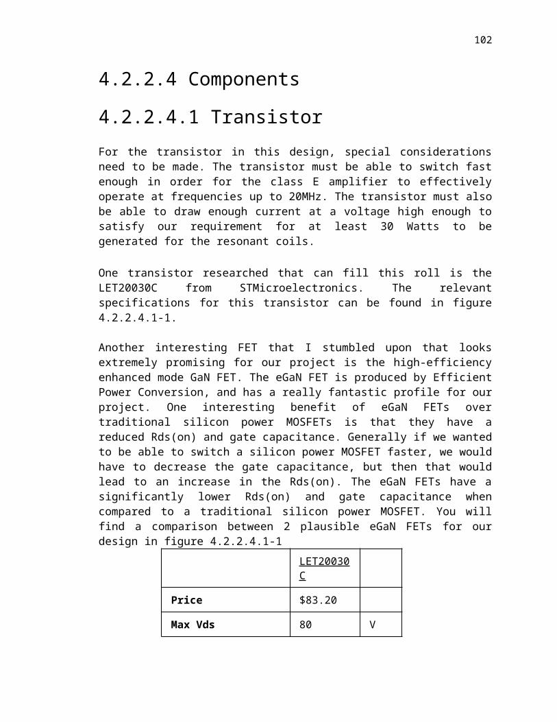
108
Figure 4.6.2-1 Single Supply ApproachFrom the work of: High-Voltage Signal Conditioning for Differential ADCs, by: Pete Wilson, P.E.
Figure 4.6.2-2 modular approachFrom the work of: High-Voltage Signal Conditioning for Differential ADCs, by: Pete Wilson, P.E.

109
Figure 4.6.2-3 fully differential approachFrom the work of: High-Voltage Signal Conditioning for Differential ADCs, by: Pete Wilson, P.E.
4.6.3 Wireless communication network:This section is dedicated to determining how the microcontroller will talk with the wireless sensors on the car. The issue for one thing here is that the wireless is not embedded into the microcontroller, so an external accessory is necessary. The idea of an embedded wireless was ruled out when the chip choices which offered such abilities did not fit the criteria of being flexible enough for application towards this project.
4.6.3.1 XBeeSo to choose, a familiar wireless communicator was chosen, the XBee-Pro. This small device fits a standard form factor from its predecessor, the XBee, and communicates in its traditional instance using the IEEE 804.15.4 standard. The RF receiver is also capable of Zigbee, DigiMesh, and 802.11bgn standards. Because of such compatibilities, it is the preferable choice as over Bluetooth

110
which uses proprietary frequencies and standards. Their built form the ground up to be low cost and low powered wireless network sensors.
They have for their functionality respectable cost, good range and flexibility, allowing for I/O connection as well as operate on standardized frequencies. Without additional programming, these little bees are capable of analog to digital conversion and well as digital I/O at up to a 10-bit resolution which is the same as the resolution of the PIC32MX795F512L. Quintessentially, these little things are able to act as direct leads. For testing purposes, it may be important to test compatibility beforehand by use of a simple Xbee compatibility kit which will hook up easily to a PC via a USB connector.
Power requirements for these are low at max using only 340 microamperes of power at 3.3V. In case of necessity, they come with free configuration software, as it is in technicality a microcontroller of its own right. The Xbee is ideal for use on this project as the need for remote sensing is important for the charging and discharging of the capacitor array.
Figure 4.6.3-1 Visual Representation of the XBee Form Factor (Wikipedia)
4.6.4 Display real-time data: It is important to be able to observe the data flow of this project in order for the control signal to the charge and discharge regulators have the proper actions in this system. This is not only important for the protection of the circuits, but also the efficiency of the project. The best way to observe and know the project is running properly is when these values can be observed. To do this, an analogue

111
concept can be implemented, more easily in a display system like an LCD, or nixie tubes.
Analog system would be difficult at this point when it requires ADC already, to then go digital to analog conversion (DAC) would be redundant. Although this may be the most cost effective, it would also not be the most aesthetically pleasing nor complex beyond the DAC.
Nixies tubes are an old system and would be similar to that of the analog circuit that displays but use a transistor based switching system to control the output of the nixie tube. These also require tremendous amounts of voltage, the likes of which are not possible easily driven by todays digital control standards. They still exist in normal use due to old equipment which still utilizes nixie tubes. Because of their relative age as a technology and incompatibility with the digital control, they are not a useable candidate.
Figure 4.6.4-1 Nixie Tubes (Wikipedia)
So an LCD can be determined at the best choice for displaying values on a digital format. Using a Microchip display would be preferable since this is a Microchip microcontroller. Depending on the number of outputs or print out variables needed at any given time, they screen can be programmed to work with one of two provisions from the KS0108 Controlled LCD in a 128x32 or 128x64 package. If there are more than two, the AZ Display 128x64 will be needed and if two or less are needed to be observed, then the DX Micro 128x32. For now, we will assume the AZ Display will be used as a worst-case scenario. The AZ Display is cost in at $40.

112
4.6.5 Regulate load discharge output:
Figure 4.6.5-1 Block diagram of Power and Data Flow
The process of regulating the output is a delicate balancing operation that requires significant thought as to how to maintain a constant and fluctuating voltage output of this capacitor array. The output will be heavily monitored by the microcontroller and will thusly need the ability to control the output somehow. The concept thought of so far is the use of a potentiometer as a means to voltage divide the system. By reducing the resistance slowly in the potentiometer in parallel with the main line to ground, the output into the load can be controlled to the point where a constant power draw can be maintained at a continued voltage. The circuit will be fleshed out, but the potentiometer is the most important for this segment, for if a potentiometer cannot be found, then regulation cannot happen effectively. Fortunately, a high voltage potentiometer by Analog Devices is offered

113
in the model AD7376AR10. Primarily used in industrial applications, this will be a great fit as it is durable and has high physical and electrical tolerances.
4.6.6 Short circuit charging process:A high power electrical signal will be entering the circuit as a charging current which is regulated by voltage size. It is relevant for this process due to the condition of the capacitors need to be maintained as to not overload them. Because the DC voltage does not stay constant throughout the charging process, the charging can be digitally regulated by a simple comparison until a limit is reached where the voltage reaches a critically low point and will open a shunt. This will effectively halt or maintain a voltage level through a simple sensor controlled switch on the receiving end of the inductive resonance system.
An alternative even lay in an analog shunt which will need no voltage monitoring and simply activate when the circuit feels it has reached a critical voltage level.
Analog Devices sells a more intricate and IC version of the High voltage, current shunt model AD8215WYRZ at a relatively low cost. This will be the first possibility for a power shunt for this project despite it being an analog and not digital device. It sells for $1.43
Figure 4.6.6 – 1 50A Shunt (Wikipedia)
4.6.7 Alert low voltage in capacitors:Fortunately, the alarm system can be very simple since there are two methods to use for this application. 1 can be controlled through an analog circuit which will activate when nearing a specifically determined voltage level and another would be by utilizing the voltage sensor already integrated at the end of the capacitor array to send a signal to the screen to indicate charging is needed within a certain voltage level.

114
4.6.8 Data Acquisition Budget: Category Part Parts Designation Cost Quanitity
Microcontroller chipKIT Max32™ CHIPKIT-MAX32 49.50 1PICkit™ 3 De. Exp. DV164131 52.49 1MPLAB IDE MPLAB IDE Free 1
Sensors ADC 3221 MCP3221 1.44 4OP Amp 301(5-pin) OPA301AIDBVT 0.90 8OP Amp 335(5-pin) OPA335AIDBVT 1.15 4
Wi-Comm. XBee XB24-AWI-001 19.00 2XBee USB adapter XBee-USB 27.92 1
LCD 128 x 64 AZ Display ATM2412B-NLW-FFW 40.00 1Load Discharge AD7376 AD7376AR10 4.51 2Short Circuit High voltage shunt AD8215WYRZ 4.13 1-2Alarm LED LED 0.05 1Figure 4.6-1 Budget from Data Acquisition
5. Design Summary
5.1 Power Supply
The AC to DC Converter will take our mains of supply which will be a house hold wall outlet of 120V RMS 60 Hz AC signal, and completely convert that to a DC power signal between the range of 24-28 volts. The topology chosen to implement this conversion is a MOSFET Bridge Rectifier in H-Bridge configuration. It will begin with basic 5:1 step down transformer to drop the voltage to about 33 Volts (final output will be lower and then the voltage received here to compensate for voltage drops in series components). Two N-Channel and P-Channel Power MOSFETs will be used for rectification over diodes due to their low forward impedance and voltage drop, reverse recovery time compared to diodes at the same high temperature, and their protective resistance to current surges. Finally, a smoothing capacitor and parallel load combination will be used to charge/discharge to the load will be used to project the now DC output to the next component. The parallel combination (RC) is to be determined in a lab environment; the simulators available do not take the material type into consideration and will play a role in how the DC power signal forms and ripples. Final output requirements in whole will meet following specification and requirements:

115
Converting a purely AC signal to a strong reliable DC signal. Stepping down the AC voltage level to a feasible and workable voltage in
specification range( about 33 Volts) Generating a pure DC signal with enough voltage and power output to be
fed to further components with heavy consideration of future component specification, requirements and design.
Minimal voltage loss after step down and before load output. Keep Ripple Voltage or considerably noticeable and problematic “noise” to
a minimum in which can cause a substantial amount of noise during amplification stage of the design.
Maintain an efficient amount of power dissipation across component with both safety and accuracy.
Consider the operating frequency at the point in time where this component is being used.
Insure that the components chosen will be operating as expected from the operating frequency determined in the previous step
5.2 RF Power Signal GeneratorIn developing the RF Power Signal Generator, we have determined that the best course of action would be to first generate a small signal of the desired frequency with an oscillator, then we would amplify that small signal to levels required for sufficient coupling of the resonators as well as enough power to quickly charge the RC car.
For our oscillator, we chose to utilize a programmable oscillator to generate the small power, high frequency signal that we will later amplify. We chose the programmable oscillator because it was extremely easy to adjust with a microcontroller and user interface, operated at a wide range of frequencies, and was relatively cheap and easy to implement.
The programmable oscillator that we chose was the DS1077 from Maxim Integrated. This programmable oscillator is easily available and well documented from Sparkfun, as well as cheap and operates in a frequency range quite larger than our necessary specifications. The relevant specifications of the DS1077 are shown below in figure 5.2-1. (See Next Page)
DS1077

116
Price $2.95
Frequency Range 16kHz - 133MHz
Supply Voltage 5 v
Supply Current 50 mA
Standby Current 2 uA
Power-Up Time 0.1 mS
Load Capacitance 15 pF
Operating Temperature Range negative 45 to 80 degrees C
Package 118mil μSOP
Number of Writes 10,000 minimum
Figure 5.2-1 DS1077 Specifications
In order to amplify the high frequency signal generated from the DS1077 programmable oscillator, we explored a wide variety of amplifier options. After exploring all of the common RF frequency amplification options, we determined that a class E amplifier would best suit our project because they have very high efficiency ratings, operate well into the RF range, and can effectively amplify a signal to the current levels that we need.
Our class E amplifier employs at its heart an eGaN FET by EPC ( the EPC2012), which has a high drain current, can operate at RF frequencies, has a low on resistance, and is much cheaper when compared to RF Power MOSFETs of comparable specifications. The relevant specifications of the EPC2012 are shown below in figure 5.2-2.

117
EPC2012
Price $2.98
Max Vds 200 V
Max Vgs 6 V
Max Id 3 A
Igss 0.1 mA
Ciss 128 pF
Coss 73 pF
Crss 3.3 pF
On Resistance 100 mOhm
Figure 5.2-2 EPC2012 Specifications
The output LC tank circuit of the class E amplifier, which is critical for the class E operation of the design, was determined by equations derived from the paper "Class E - A New Class of High-Efficiency Tuned Single-Ended Switching Power Amplifiers." (Sokal 7). Using these equations in matlab, we determined the component values for the LC tank circuit of the class E amplifier, and they can be found in figure 5.2-3.
Vcc= 30V
Vsc= 2V
Q= 6
P= 30 W
f= 10000000 Hz
R= 15 Ohms
L2= 1.44uH
C1= 194pF
C2= 240pF

118
Figure 5.2-3 LC Tank Circuit Component Values
With these components and a SPICE model of the EPC2012 eGaN FET, we simulated the class E amplifier in Multisim to verify the functionality of the design at the desired frequency. Figure 5.2-4 depicts the simulated schematic, 5.2-5 shows the output and input waveforms, and figure 5.2-6 shows the wattmeter output.
Figure 5.2-4 Class E Amplifier Multisim

119
Figure 5.2-5 Class E Amplifier Oscilloscope Output
Figure 5.2-6 Class E Amplifier Wattmeter Output
With the functionality of the class E amplifier proven, I went on to choose the other components for the class E amplifier that would fulfill our design requirements. The general selection criteria for the components was that they had to handle currents upwards of 3 amps, voltages up to 40 volts (just in case), the tighter the tolerances the better, and of course, the lower the price the better. With these things in mind, I found the best parts for our design, which are shown in figure 5.2-7.
Part Number Description Quantity Manufacturer Vendor Unit Cost($) Lead Time
EPC2012 eGaN FET 1 EPC Digikey 2.98 In Stock
DS1077 Programmable Oscillator 1 Maxim Integrated Sparkfun 2.95 In Stock
HPI 13 Inductor 1 Wurth Digikey 3.57 In Stock
WE-HCI Inductor 1 Wurth Digikey 6.83 In Stock
SQCFVA241 Capacitor 1 AVX Corp. Digikey 1.45 In Stock
Figure 5.2-7 Class E Amplifier Components
With these components, the final schematic of the class E amplifier, with all of the necessary components are shown in figure 5.2-8. (See Next Page)

120
Figure 5.2-8 Class E Schematic with Components
One last key consideration in the RF Power Signal Generator is the driving of the eGaN FET into ‘on’ and ‘off’ mode at high frequencies. The small signal from the DS1077 does not carry enough current to fully turn the EPC2012 eGaN FET on and off at such high frequencies.
After exploring many options such as using class A amplifiers to step up the small signal from the DS1077 to current levels able to switch the EPC2012 eGaN FET at high enough frequencies, I determined that the best course of action was to utilize a gate driver, which is specifically designed for taking small signals from IC’s such as a programmable oscillator or microcontroller, and outputting that signal at current levels high enough to drive high power RF FETs into ‘on’ and ‘off’ modes at high frequencies. The specifications we set for determining the correct gate driver for our design are:
1. Delay Time below 50ns (equivalent to 20MHz)2. Current peak above 1A3. Inverting or Non-inverting input type4. Availability5. Price6. No more than 2 outputs; only one needed

121
With these specifications, we determined that the TC4421AVOA from Microchip is best suited for our design at its price point. Its relevant specifications are shown in figure 5.2-9.
Input Type Delay Time Current-Peak Number of Outputs Price
TC4421AVOA Inverting 38ns 10A 1 $2
Figure 5.2-9 Gate Driver Specifications
5.3 Magnetic Resonant CoilsThe MRC network is able to be modeled as a transformer network, and will be treated as such. The only difference is that we will not be directly implanting resistors in our network, and will instead use the ESR of the components in series for our calculations. The lower the ESR, the higher the Q factor and thus the better the transmission, so naturally we want ESR to stay low. The capacitors will be a surface mount model and the inductors are to be fabricated by us.
As stated in the design section, we are going to be using a PTFE material base to lithograph the inductors into. PTFE naturally has a large relative magnetic permittivity, which is ideal for our design. Recall that inductors do not link through electric fields, rather through magnetic fields. While not the most ideal permittivity, it is a stable material that can easily be lithographed, that can stand large amounts of electric current, and is relatively inexpensive. It should also be noted that when constructed, the very nature of this design will cause a small amount of capacitance that is to be measured before attempting to select a capacitor for impedance matching. This equivalent capacitance comes from the spaces between the coils on the inductors themselves.
For specific capacitances to be used within the MRC, we have to first determine the inductance of our resonators, and that will come with testing next semester. However, there is a set of capacitors from Murata Electronics North America called the ERB line, which boasts a high-Q value and high voltage tolerance, as well as being ideal for anything in the 1MHz to 1GHz application range, making it perfect for our purposes. Below is a datasheet segment from muRata Electronics North America, specifically the 12pF model.

122
Figure 5.3.1 - ERB Series Capacitor features courtesy of muRata Americas
These capacitors are solder able onto a PCB, and able to tolerate large amounts of voltage and frequency, as well as heat and power. Once we’ve determined how much inductance our transmitter and receiver coils will be, we can determine what our capacitor should be in order to set the resonant frequency to what it should be. This general set of capacitors serves our purposes well.
5.4 RF Power to DC PowerThe RF Power to DC Power component will be used after the RF signal has been received from the second coupled inductor and its purpose is to rectify the signal for the second time in order to charge our capacitor array quickly and efficiently. This topology will reflect the basic Diode Rectifier Bridge only we will be replacing the simple diodes with high Frequency Schottky Diodes (SK311A). Unlike simple diodes which are exhibit capacitive qualities at high frequencies in turn affecting the reverse recover time and DC output, these Schottky diodes are meant to operate at high frequencies with a low forward voltage and very fast reverse recovery time. This will enable the signal to properly rectify alongside a parallel resistor/capacitor combination with minimal noise. The RC combination will be determined in a lab environment; the simulators available do not compensate for the type of material that then components are made with. The final output will meet the following requirements:
The DC signal must be strong and reliable with minimal noise. The current draw of the output is 3 A MAX. The components used in the rectification process must be able to handle
the very high frequency by having a very short reverse recovery time. The Smoothing capacitor and parallel load must be adjusted adequately
Enough to meet the second specification point and maintain proper charge/discharge rate.

123
5.5 Capacitor ArraySomething nice about the rated value that Maxwell Technologies has done is that they have given a rated value below the absolute maximum voltage, which means the voltage we are shooting for is even safer. According to the datasheet, we would be safe up to 8.55V, and we’re only charging the caps to 8V.
These capacitors are rated at 3.2m-ohms of ESR. While this is still a very low resistance compared to our load (which is 5-ohms), and the rest of our circuitry, it is still fairly high for a capacitor, which usually has tenths of milliohms if not hundredths of milliohms of ESR. For our current design, this isn’t an issue since we aren’t drawing a large amount of power. However, it will become an issue should we decide to increase the power of our source, as the caps will begin to heat up too much greater temperatures.
The capacitors also have a relatively low leakage resistance. Rated at 2.7V with a leakage current of 0.3mA, these caps have a leakage resistance of approximately 9k-ohms, well below the desired mega- or even gigaohm range. However, considering the large amount of charge they can hold, this isn’t an issue. The caps lose less than 1 micro-volt per second at this rate. This is still the maximum leakage current rate, and only applies when the cap is fully charged and left alone. it would take more than 15 million seconds to fully discharge one of these caps, or roughly 180 days, which is about 6 months. Not only does this easily beat the average discharge time of most batteries out there, which is about 2 weeks to 1 month, but it would be far less painful to recharge one of these caps for roughly 10 minutes than to recharge a battery pack for 3-4 hours.
Lastly, we see that the cap is safe up to a short of 220A, Listed in Figure 4.5.6. We have no plans for the caps to ever reach such a current, but it is still a great feature to have. The problem a lot of people have with RC cars is that turning while moving can sometimes put a great deal of stress on the battery pack because performing both functions under load at the same time is often too much for a battery pack. With caps, this would no longer be an issue, since the caps would be able to supply this type of current immediately. As a matter of fact, this load would be well within the 24A safe continuous current draw, so the capacitors are better suited to this kind of use by design. We actually found small capacitor banks available to RC car enthusiasts that will store a temporary charge to negate such a problem. Now the client wouldn’t need to purchase an after-market array.

124
5.6 Design Summary of Data Acquisition:In short, the design of the data acquisition system has many parts which require synchronizing from sensors to controllers and finally the brain which needs to coordinate all of them together. A major hurdle alone was to find a brain chip compatible with the needs of the project. It needed many peripheral functions and access points as well as being advanced enough for the ability of a low budget project like this wireless energy transfer project to 80MHz be able to access such powerful computational power of an embedded chip. The PIC32MX795F512L in the ChipKit MAX32™ turned out to be a marvelous find which will be a great addition to the project. It will include the express debugger for fast and easy startup of this project.
To add to this, the sensors required redundancy. So to do so, the built in ADC were augmented with external ADC to allow the I/O to be simple digital I/O and allow the risk of burn-out to happen away from the microcontroller. This places only the op-amps and MCP3221 ADC in a single supply configuration at risk which cost significantly less than the ChipKit MAX32™ were to be lost in an accident.
For wireless autonomy, a method needed to be devised. Wire was out of the question as it could be misconstrued and defeat the purpose of wireless energy of eliminating that concept of autonomy. The microcontroller integrated wireless would not allow for enough power or memory within the chip to be right for this project so an alternate method had to be made. Thus the XBee is chosen as the method of choice for wireless communication. With easy integration into the project by way of pre-programmed and pre-linked XBee modules, it is a no-brainer as to why it is a good decision to use an XBee to be able to network the autonomous car sensors with the main microcontroller.
The LCD required will heavily depend on the needs of the project. If more outputs are necessary, then a larger AD Display will be needed. But it’s smaller brother the DX Micro screen plays an equally viable use in this project. Coding load will wade heavily on this aspect, but regardless, a monochromatic screen is a good enough fit for the scope of this project. This model of screens also benefit from a large base of experienced programmers who have experimented with these easy to use modules.
To manage load discharge, what is most important is to understand just how imperative it is to find the right potentiometer to fit this high voltage and high current job. So the AD7376AR10 was decided upon to be the best choice for this project. It will be used in a circuit which will work closely with the recharge alarm to determine when the limits of charging as well as saving the life length of the capacitors.

125
To control the charging, a voltage shunt will be needed. So a chosen AD8215 was chosen as an early testing model for this very purpose. It will be used in tandem with a digitally fed voltage sensor at the note before the capacitor array in order to make sure that the array is nearing the capacitor arrays voltage limit.
5.7 PCB BoardWe have determined that the best PCB manufacturer for our project is 4pcb.com. The reason was chosen 4pcb.com is because it is the only PCB manufacturer that offered a student discount, and quite a good one as well! It’s only $33 for a 2-layer PCB board and $66 for a 4-layer PCB board. For our project we will only need 2-layer PCB boards, so this will be an excellent option.
Some considerations to take when ordering with 4pcb.com is that they have a 5 day turnaround time, which we need to consider with our deadlines, and that does not include the shipping, so it would be wise to take into account 2 weeks when considering arrival time of the PCB to make sure that it is on time as expected, and to account for any possible delays. Another consideration about using 4pcb.com is that when we utilize their student program, we have to ship the PCB board to a university address, so we will have to arrange for the PCBs to be sent to the university campus and for us to retrieve it upon arrival.
Probably the most popular PCB software in the market right now is EAGLE, and this is simply because it’s a very powerful, well documented piece of software and best of all, it’s a freeware license, and therefore it’s completely free. It also outputs in the entire popular PCB layout file types that many PCB manufacturers use, and is has a massive component library available online. It has a huge following, and therefore a lot of support, documentation, and tutorials can be found online.
6. Testing
6.1 Power SupplyThe testing scheme for the power supply is to simply build the circuit onto a breadboard once all the parts have arrived with a load resistor in place for the rest of the project. Once the output signal is found to be correct, we can remove the load resistor and connect the rest of the project, such as the class E amplifier once it has been deemed functionally correct. With the class E amplifier connected, we can test the operation of the class E amplifier as it’s being powered by the power supply being directly connected to the wall outlet.

126
6.2 RF Power Signal GeneratorFor testing the RF power signal Generator, it would be wisest to test the functional correctness of the design before finalizing it into a PCB. Therefore, our plan will be to utilize breadboards to test the functional correctness of the RF Power Signal Generator, and once functional correctness has been achieved, it can be finalized into a PCB, and then retested to ensure functional correctness.
6.2.1 Functionality TestingOnce all of the required parts have been procured, and before the design can be finalized into a PCB, the functional correctness must be confirmed for our specifications. To do this, we will utilize breadboards to layout the components for the design of the class E amplifier and utilize the function generator, DC power supply, and the oscilloscopes in the Senior Design lab to test, alter, redesign, and confirm the functional correctness of our class E amplifier.Once the class E amplifier is confirmed to operate appropriately, we can remove the function generator, and utilize the programmable oscillator and gate drivers to test the functional correctness of the amplifier and oscillator components.Once the class E amplifier and oscillator components are confirmed to conform to our designs, we can utilize our own stand-alone power supply we've designed to power the oscillator and class E amplifier from 120V 60Hz AC mains from the wall outlet. Once all of this has been confirmed, or redesigned to conform to our specifications and requirements, we can move on to prototype testing.
6.2.2 Prototype TestingOnce all of the components and topologies of the major sections of the RF power signal generator have been confirmed to conform to our designs, we can finally implement them onto the custom PCB board designed for our project.Once everything has been soldered on, we can then test the final prototype RF power signal generator simply by hooking it up to the AC wall outlet mains, and testing the output of the amplifier. If any abnormalities arise, we will have to debug which components, or sections are having problems with the PCB layout.
6.3 Magnetic Coupled ResonatorsIn order to test our MCR network, we have several key features that must be examined. First, we must make sure that the MCR network is properly transmitting power between the transmitter and the receiver. Next, we will test to make sure that the MCR network operates at the resonant frequency we have set by the system. Once that has been done, we have to test that this network works at the distance at which we need it to be. After that, we need to examine

127
ways of making it more efficient. Finally, we have to test to make sure we can successfully utilize the power it is transmitting.
To test proper transmission, we will first have our planar inductors lithographed, and then attach impedance matched capacitors. Then, we will attach a function generator to the transmitting coil network, setting the amplitude of our wave to 10V+. Most function generators on campus can only go as high as 10V, so this may be the maximum we can test for now, which is fine. We will then place the resonator network in a manner that it is able to pick up the transmitted power signal. Lastly, we will observe the received signal with an oscilloscope to measure and view the received signal to ensure that it is useable and efficient.
To test resonant frequency, we will set the function generator to 10MHz and observe the efficiency of the system. From there, we will change out the capacitors to nearby values and see their effect on the efficiency. Due to the mutual inductance caused by their proximity, it is quite possible that the resonant frequency of the system will not be exactly 10MHz, and so we may need to adjust the capacitance accordingly.
At this point, we will also want to test the transmission at the exact same distance as the bottom of the car’s chassis to the ground, which is roughly 1.5 inches and observe the mutual inductance here. We will also be using 3 different sets of inductors: 4 inch diameter, 2 inch diameter, and 1 inch diameter. According to our studies, the 1 inch diameter model would be the most efficient in theory, but the 4 inch model may come out on time once mutual inductance becomes a factor.
Next we will work on efficiency testing. We will observe the effects of nearby frequencies and see what their efficiency is. If we find that mutual inductance has interfered, we will further manipulate the capacitance value until we can make sure that the design is most efficient at 10MHz. From there, we will attach the RF power to DC converter network and ensure we are getting a DC signal of sufficient power. After that, we will attach the oscillator network to the transmitter network and supply it with the required DC power. Lastly, we will attach our AC/DC converter and ensure that it still works as it should. After all of this, we may continue to mess with the capacitance values to make sure we’re getting the most efficiency possible.
Once all of those networks have been combined and are shown to work, we attach a load to the final stage of the system. Here, we’ll make sure that the system is not only able to transmit the DC power signal needed for the capacitor array, but we’ll also make sure that it can do so consistently under load. We will do a “burn-in” test of sorts and power a device such as a light-bulb for several hours. Once that’s done, we’ll later attach the capacitor array as outlined in the Capacitor Array test section.

128
6.4 RF Power to DC PowerIn order to test the RF Power to DC power converter, we must first obtain through a function generator a signal of frequency in the range of 1MHz to 20MHz and observe its true value through and oscilloscope. Once this has been achieved we will double check to make sure that our circuit configuration is correct and connect the function generator to the input of the converter. Using the oscilloscope, we will observe the output of the converter by measuring the voltage signal across the parallel load. The expected signal should be a clear and reliable DC power signal with minimal noise.
In addition, the will mimic the load of the charging capacitor array with another load in series with another power load. This can be done using a resistance comparable to the capacitor array and its designed circuitry. This load should have a current draw of 3 Amp max. This will be enough to charge the capacitor array fast enough to meet the specifications and requirements of the next component which is: the Capacitor Array.
6.5 Capacitor ArrayIn testing the capacitor array, several key features need to be examined before we proceed with the actual construction of our prototype. First, the capacitors must be tested for accuracy. Their precise capacitances must be tested to ensure that we are getting the proper run time out of our system. This can be measured using a DMM with a capacitance testing mode, which is fairly standard. We will test the individual capacitances as well as the capacitance of the entire array.
Second, we need to make sure that the capacitors are safe up to 8V for normal operation. This will come from a “burn-in” test of sorts. We will charge the capacitors to 8V, leave them for an extended period of time, and allow them to dissipate. We will repeat this test several times over to ensure that the capacitors successfully and consistently charge to their desired voltage through their own mechanisms, which will help us determine later if a charging issue is related to the circuitry, or to the capacitors themselves. We will also make sure that they are not going to overheat in this process. Considering the ESR of 3.2-milliohms with 2-3A of current passing through it, the collected heat should only be in the order of 10s of milliwatts, but it would better to find a malfunction before placing the capacitors on the car.
Third, we need to test that the car is able to handle effectively the current coming from the capacitor array. For this test, after testing the capacitance and ensuring they charge/discharge as they should, we will connect the capacitors, and only the capacitors, to the car in place of the battery pack. We will then run the car

129
until it is no longer running. From there, we will measure the voltage remaining on the capacitors. It is possible that the car is able to run at some voltage below 6V, and that the 6V value of the battery is merely a safe operating voltage, not necessarily the required voltage. This test will also demonstrate this minimum operating voltage to us.
After the operating test comes the test to see if the protector circuit works. For this one, we will connect an established DC source above the absolute maximum rating of the caps. We will carefully monitor, using a DMM, the voltage across the capacitor array once the protector circuit has been connected between it and the power supply. If it should reach more than 8V, we will know the protector circuit has failed and we will know to fix this circuit before proceeding. Once we have a working protector circuit, we can move on to the LED warning light circuit.
To test the LED warning light circuit, we will charge the caps to above the reference voltage value, currently set to 6V but subject to change. Once set to that value, we will allow the capacitor to discharge until it reaches threshold and make sure that it then causes the LED to light. Once we see that the LED is lit successfully, we will then monitor how long it stays on afterwards, and see if it matches our predictions.
After all of that is finally done and tested, we can then move on to seeing if our wireless charging mechanism can successfully charge the car. To test this, we will then connect all of the circuits and make sure we can directly charge the capacitors with all other circuit elements attached to it, including, but not limited to, the protector circuit, the LED warning circuit, the wireless communication sensor, and the RC car itself. Once all of that is working, we will then connect it to the receiving magnetic coupling resonator followed by the RF power to DC converter to ensure that the capacitor array is successfully being charged by the MRC network. At this point, we will know we have a working model for a wirelessly, quickly charged RC car.
6.6 Data Acquisition:Testing will need to be done in sections and in phases.
1. The first phase will need to determine if we have a satisfactory brain for use on this project. For that to be done, test codes and simple tasks will be run through the microcontroller prototyping kit.
2. Some simple tests must be done to determine of the single source ADC voltage sensors are viable and will not destroy the circuitry that makes this a relevant addition to the project. It could prove to be a point of failure or a point of great success, but they are next. This will be tested using DC power supply tester and observation equipment.

130
3. Next the Discharge regulator will need to be tested. A small scale super capacitor system can be prototyped so we can test the validity of the potentiometer regulation circuit. If this fails we can go another route. But if it works, then it is assured that we have a safe and viable method to control the flow of power from the super high capacity capacitors. This will need to be done in the confines of a lab and precautions must be made to protect the Microcontroller.
4. Wireless capability must be determined and verify that no interference comes in between the car and the data transmission lines. Secondary are the foreign signals that will pollute the air at the same time as the data line transmissions and potentially at the same frequencies. This requires sample signals be run into the remote ADC connected to the microcontroller via XBee‘s for voltage sensing verification.
Secondary signals will be tested by providing other signals into the air at their respective frequencies to observe influence from foreign emitters.
5. Charging controls will be tested next on the instance of whether there needs to be something more exhausting than a shunt required. A shunt itself is an analog part, but a diversion circuit might be necessary for our power consumption. It will be tested without the microcontroller to begin with, to see the physical limit of the shunt, and then go to something more controllable afterwards.
6. Integration testing will be the final step as all of these functionalities must be able to work together on the board at one time.
7. Prototype ConstructionIn the following sections we will be discussing the development of our final fully built prototype wireless power transfer system, with the ability to power an radio controlled car. We will go over the materials we have deemed necessary to acquire, our plan of acquirement, our method of PCB board development, final assembly, and any other key considerations relevant to our project.

131
7.1 Bill of MaterialsPart Number: Description: Quantity: Unit Cost($): Total Cost($):EPC2012 eGaN FET 1 2.98 2.98DS1077 Programmable
Oscillator1 2.95 2.95
HPI 13 Inductor 1 3.57 3.57WE-HCI Inductor 1 6.83 6.83SQCFVA241 Capacitor 1 1.45 1.45TC4421AVOA Gate Driver 1 2 2XB24-AWI-001 Xbee (set) 2 19 38MCP3221 ADC 4 1.44 5.76DV164131 PICkit3 Express
Debug1 69.99 69.99
PIC32MX795F512
chipKIT Max32™ Prototyping Platform
1 49.5 49.5
1/10 size RC car RC car 1 50 50PCB Boards PCB Boards 2 33 66MPLAB IDE MPLAB IDE 1 0 0SI2300 N-Channel MOSFET 1 1 1BCAP0350 Supercapacitor 6 13.11 78.66RL5-R8030 5mm Super Bright
LED1 0.59 0.59
LM4040Ax0 3V(x=3)Precision Voltage Reference
1 0.74 0.74
LM4040Ax0 5V(x= 5)Precision Voltage Reference
1 0.74 0.74
ERB218 series Ceramic high-Q capacitors
2 0.5 1
SK310A HF Diodes 8 0.61 4.88ADC 3221 MCP3221 4 1.44 5.76OPA301AIDBVT OPAmp301(5-in) 8 0.9 7.2OPA335AIDBVT OP Amp 335(5-pin) 4 1.15 4.6ATM2412B-NLW-FFW
128 x 64 AZ Display 1 40 40
XBee-USB XBee USB adapter 1 27.92 27.92AD7376AR10 AD7376 2 4.51 9.02AD8215WYRZ High voltage shunt 2 4.13 8.26SK310A-LTP Schottky Diode 4 0.61 2.44CSD18532Q5B N-Channel MOSFET 2 1.13625 2.2725CSD25211W1015 P-Channel MOSFET 2 0.33 0.66
Totoal Cost: 494.7725Figure 7.1-1 Table of Cost Break Down

132
7.2 Procurement of PartsUtilizing the vendors given in the Bill of Materials, we will begin procuring parts this summer in order to begin initial development and testing of our designs for the project. If the parts that we’ve selected become suddenly difficult to obtain, we will attempt to procure those parts from other various venders. For instance, if a part is out of stock at Digi-Key, we would attempt to procure it from Mouser. If we are unable to obtain the part from a reputable vendor, it would then be necessary to find a suitable replacement for the part unable to be obtained. This is why we are going to begin procurement early this summer instead of waiting for Senior Design 2 to begin this fall. Too many times logistical fallacies crop up in the middle of developing a project, and we are attempting to minimize such occurrences.
We also need to consider in the procurement of our parts the amount of time that it may take a particular vendor to deliver our order. In many situations, I have found that part vendors tend to take longer to deliver parts than normal consumer stores such as Amazon. This is another reason that we are going to begin gathering the necessary parts for our project this summer as opposed to waiting this fall.
We will also be purchasing an excess of parts cheap enough to be deemed worthy. This is to ensure that we have spares for most of our parts. With these spares, we can be sure that we will not have to panic and overnight parts if a eGaN FET were to suddenly malfunction on the final week of construction. We are basically trying to make sure to minimize any opportunity for negative situations to crop up in our project construction; we want it to be as straightforward and as easy of a time as possible. Although this is not completely possible, we believe that spending the extra time in the early stages to try and minimize potential problems; will undoubtedly pay off in less headaches in the end.
7.3 PCB Development of the PCB board for our project requires two key considerations to be explored in order to be best prepared for the eventual development of our final construction of our project, which will require at least two PCB boards to properly function to spec.
We must first explore different PCB manufacturing foundries, and then we can research different EDA tools for PCB development. The reason that we must explore the different PCB manufacturing foundries first is because that will determine what EDA tools we can use because some foundries require the use of their own PCB development software, and therefore we would just have to use that to develop our PCB board. If the PCB manufacturing foundry doesn’t require

133
specific software of file type, then we would be free to explore all options of PCB development software.
7.3.1 PCB Manufacturing FoundriesIn considering which PCB manufacturing foundry to choose when we are ready to manufacture our PCB boards, there are a few considerations to take into account. First, we don’t have to worry too much about the quality of the PCB board, as most reputable PCB manufacturers produce reliable products, and we can pretty much be sure that our PCB board will be up to par as long as we don’t order a PCB board from some random Chinese manufacturer or a guy on craigslist.
With that in mind, Price is going to be the biggest concern with our choice in a PCB manufacturer. We have to take into account that we only need 1 of each board and most PCB manufacturers operate by making PCB boards in massive bulk up to millions, so they generally charge extra fees for such small quantities as 1, so we should be on the lookout for PCB manufacturers that are friendly to small quantity customers, or even provide student discounts, since that would be applicable to us. Aside from price, we also need to consider the types of development software that they accept or if they require their own development software.
Taking into account the considerations laid out above, we have determined that the best PCB manufacturer for our project is 4pcb.com. The reason was chosen 4pcb.com is because it is the only PCB manufacturer that offered a student discount, and quite a good one as well! It’s only $33 for a 2-layer PCB board and $66 for a 4-layer PCB board. For our project we will only need 2-layer PCB boards, so this will be an excellent option.
Some considerations to take when ordering with 4pcb.com is that they have a 5 day turnaround time, which we need to consider with our deadlines, and that does not include the shipping, so it would be wise to take into account 2 weeks when considering arrival time of the PCB to make sure that it is on time as expected, and to account for any possible delays. Another consideration about using 4pcb.com is that when we utilize their student program, we have to ship the PCB board to a university address, so we will have to arrange for the PCBs to be sent to the university campus and for us to retrieve it upon arrival.
7.3.2 PCB SoftwareWhen choosing which PCB software we are going to use when developing our PCB board, our first consideration is what PCB EDA tools our preferred PCB manufacturer accepts. Lucky for us, our preferred PCB manufacturer, 4pcb.com,

134
accepts all of the major PCB layout formats, as well as they have their own PCB CAD tools called PCB Artist which has a large amount of parts already on file and ready to be routed, so PCB Artist is certainly an option to consider when determining which PCB software we want to use for our project.
Probably the most popular PCB software in the market right now is EAGLE, and this is simply because it’s a very powerful, well documented piece of software and best of all, it’s a freeware license, and therefore it’s completely free. It also outputs in the entire popular PCB layout file types that many PCB manufacturers use, and is has a massive component library available online. It has a huge following, and therefore a lot of support, documentation, and tutorials can be found online.
Comparing the two best options for developing the PCB boards for our software, I believe that EAGLE is the best option for us. It’s long history gives it much more documentation and tutorials than PCB Artist would, and it’s such a popular platform that pretty much any component is ready to be implemented into EAGLE with all of the support that it has online. It’s this support that makes it seem to be the better choice than PCB Artist, but honestly both of the softwares are free, so why not just download them both, try them out, and stick to whichever one seems to suit us the best. Both of them are supported by 4pcb.com, and seem to be pretty good software.
7.4 AssemblyOnce we have fully tested the functionality of all of the components of our project, then had PCB boards made and components soldered, and finally had those PCB boards and components tested for the correct functionality, it will finally be time to fully assemble our entire project.
We will first need to assemble the power supply, station microcontroller, as well as the oscillator and amplifier all to one station. This will most likely be a box with an LCD screen and keypad input. This will make up the base station that will take the 120V AC mains from an outlet and convert it into a high frequency power signal to be sent to the resonator coil, which will be affixed horizontally in order for the RC car to ride over it to begin the charging.
Once the base station has been assembled and checked that it is still working correctly, we can begin modifying the RC car for our project. Modifying the RC car for our project will entail replacing the rechargeable battery on board with the supercapacitor array, affixing the receiving resonator coil to the underbody of the RC car, and attaching, securing, and connecting the relevant PCB board designed to go onto the RC car.

135
Once everything is in place and fully assembled, we can again test the full functionality of the design and observe if it imitates the results that we determined in the lab. If everything is according to spec, then we will have a fully functioning wirelessly charging RC car, and our project will be complete!

Permissions:
A.1 Wikipedia:
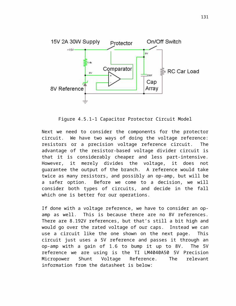
b

c
A.2 UBM LLC (DesignNews.com):
A.3 Vishay Siliconix:

d
A.4 Texas Instruments:
IMPORTANT NOTICETexas Instruments Incorporated and its subsidiaries (TI) reserve the right to make corrections, modifications, enhancements, improvements, and other changes to its products and services at any time and to discontinue any product or service without notice. Customers should obtain the latest relevant information before placing orders and should verify that such information is current and complete. All products are sold subject to TI’s terms and conditions of sale supplied at the time of order acknowledgment.
TI warrants performance of its hardware products to the specifications applicable at the time of sale in accordance with TI’s standard warranty. Testing and other quality control techniques are used to the extent TI deems necessary to support this warranty. Except where mandated by government requirements, testing of all parameters of each product is not necessarily performed.
TI assumes no liability for applications assistance or customer product design. Customers are responsible for their products and applications using TI components. To minimize the risks associated with customer products and applications, customers should provide adequate design and operating safeguards.
TI does not warrant or represent that any license, either express or implied, is granted under any TI patent right, copyright, mask work right, or other TI intellectual property right relating to any combination, machine, or process in which TI products or services are used. Information published by TI regarding third-party products or services does not constitute a license from TI to use such products or services or a warranty or endorsement thereof. Use of such information may require a license from a third party under the patents or other intellectual property of the third party, or a license from TI under the patents or other intellectual property of TI.
Reproduction of information in TI data books or data sheets is permissible only if reproduction is withoutalteration and is accompanied by all associated warranties, conditions, limitations, and notices. Reproduction of this information with alteration is an unfair and deceptive business practice. TI is not responsible or liable for such altered documentation.
Resale of TI products or services with statements different from or beyond the parameters stated by TI for that product or service voids all express and any implied warranties for the associated TI product or service and is an unfair and deceptive business practice. TI is not responsible or liable for any such statements.
Following are URLs where you can obtain information on other Texas Instruments products and applicationsolutions:
Products ApplicationsAmplifiers amplifier.ti.com Audio www.ti.com/audioData Converters dataconverter.ti.com Automotive www.ti.com/automotiveDSP dsp.ti.com Broadband www.ti.com/broadbandInterface interface.ti.com Digital Control www.ti.com/digitalcontrolLogic logic.ti.com Military www.ti.com/militaryPower Mgmt power.ti.com Optical Networking www.ti.com/opticalnetworkMicrocontrollers microcontroller.ti.com Security www.ti.com/security
Telephony www.ti.com/telephonyVideo & Imaging www.ti.com/videoWireless www.ti.com/wireless
Mailing Address: Texas InstrumentsPost Office Box 655303 Dallas, Texas 75265
Copyright 2004, Texas Instruments Incorporated

e
Appendix B: FiguresFigure 3.2.2.1-1 Multisim Schematic of Linear Voltage Regulator with Alternating Current Input 13Figure 3.2.2.1-2 Multisim Output Voltage of Linear Voltage Regulator with Alternating Current vs. Time 13Figure 3.2.1.2-1 Switching Voltage Regulator with and Alternating Current Input 14Figure 3.2.1.2-2 Output of Switching Voltage Regulator with Alternating Current Input 15Figure 3.2.1.3-1 Step down Transformer with a Two to One Turn Ratio 16Figure 3.2.1.3-2 The 2:1 Step down Transformer Output 17Figure 3.2.2.1-1 Diode Bridge with Smoothing Capacitor 18Figure 3.2.2.1-2 Output of the AC/DC diode Bridge with a clean DC signal 18Figure 3.2.2.3-1 Power MOSFET Bridge Consisting of Two N Channel and Two P Channel Power MOSFETS 19Figure 3.3.1.1-1 Equivalent Crystal Oscillator Circuit 22Figure 3.3.1.1-2 Pierce Oscillator 23Figure 3.3.1.2-1 Hartley Oscillator 24Figure 3.3.1.2-2 Colpitts Oscillator 24Figure 3.3.1.2-3 Clapp Oscillator 24Figure 3.3.2.1-1 Class A Amplifier 27Figure 3.3.2.2-1 Class C Amplifier 28Figure 3.3.2.3-1 Class D Amplifier 28Figure 3.3.2.4-1 Class E Amplifier Topology 29Figure 3.4-1 (1, 2, 3) Square Planar Inductor Geometry vs. Efficiency 33Figure 3.4-2 Model of car driving over inductive road 35Figure 3.6.1 Power Density vs. Energy Density for Batteries/Capacitors 38Figure 3.6.2 Picture of 350F Supercapacitors from Maxwell Technologies 39Figure 3.6.3 Standard Non-Ideal Model for Capacitors 41Figure 3.7.1-1 Data Collection and Power Flow 45Figure 4.1.3-1 MOSFET Bridge Rectifier in H-Bridge Configuration 63Figure 4.1.4 – 1 CSD18532Q5B 64Figure 4.1.4 – 2 CSD25211W1015 65Figure 4.2.1.2-1 DS1077 Programmable Oscillator Specs 66Figure 4.2.2.2-1 Class E Amplifier Component Equations 68Figure 4.2.2.2-2 Class E Amplifier Component Values 68Figure 4.2.2.3-1 Designed Class E Amplifier in Multisim 69Figure 4.2.2.3-2 Oscilloscope Output from Class E Multisim Simulation 70Figure 4.2.2.3-3 Wattmeter Power Output from Class E Multisim Simulation 70Figure 4.2.2.4.1-1 LET20030C Specifications 71Figure 4.2.2.4.1-2 eGaN FET Specifications 72Figure 4.2.2.4.2-1 Possible LC Tank Circuit Inductor 73Figure 4.2.2.4.2-2 Possible RF Choke Inductors 73Figure 4.2.2.4.3-1 Possible Capacitor 74Figure 4.2.2.5-1 Final Class E Amplifier Schematic 75Figure 4.2.2.5-2 Class E Amplifier Price 75Figure 4.2.3.2-1 Possible Gate Drivers 76Figure 4.3.1 MRC Network Equivalent Model 79Figure 4.3.1-1 ERB Series Capacitor Features 80Figure 4.3.1-2 2-Coil Network Model 80Figure 4.3.2-1 4-Coil Network Model 82Figure 4.4.3-1 Power Supply Schematic 83Figure 4.4.4-1 Schottky Diodes 84Figure 4.5-1 Capacitor Charge Rate 85Figure 4.5-2 Protector Circuit Model 86Figure 4.5-3 LED Warning Circuit Model 87Figure 4.5-4 Physical Specs of Capacitors 88Figure 4.5-5 Equations for Capacitor Useable Energy 89

f
Figure 4.5.6 Electrical Specs of Capacitors 90Figure 4.5.1-1 Equivalent Model of Protector Circuit 91Figure 4.5.1-2 Recommended Operating Conditions of LM4040 5V Reference 92Figure 4.5.1-3 Electrical Characteristics of LM4040 5V Reference 92Figure 4.5.1-4 Voltage Reference Model Using Op-Amp 93Figure 4.5.1-5 LM397 Comparator Maximum Ratings Info 94Figure 4.5.1-6 LM397 Comparator Operating Ratings Info 94Figure 4.5.1-7 LM397 Comparator Electrical Characteristics Info 95Figure 4.5.1-8 SI2300 N-Channel MOSFET Maximum Ratings Info 97Figure 4.5.1-9 SI2300 N-Channel MOSFET Static Specs 97Figure 4.5.2-1 Equivalent Model of LED Warning Circuit 98Figure 4.5.2-2 RL5-R030 5mm Red LED Spec Sheet 99Figure 4.5.2-3 LM4040 3V Reference Electrical Characteristics Sheet 100Figure 4.6.1-1 Parallel Table Comparison of Four Leaving 32-bit And 16-bit Designs 104Figure 4.6.2-1 Single Supply Approach 108Figure 4.6.2-2 Modular Approach 108Figure 4.6.2-3 Fully Differential Approach 109Figure 4.6.3-1 Visual Representation of the XBee Form Factor 110Figure 4.6.4-1 Nixie Tubes 111Figure 4.6.5-1 Block diagram of Power and Data Flow 112Figure 4.6.6-1 150A Shunt 113Figure 4.6-1 Budget from Data Acquisition 114Figure 5.2-1 DS1077 Specifications 116Figure 5.2-2 EPC2012 Specifications 117Figure 5.2-3 LC Tank Circuit Component Values 117Figure 5.2-4 Class E Amplifier Multisim 118Figure 5.2-5 Class E Amplifier Oscilloscope Output 118Figure 5.2-6 Class E Amplifier Wattmeter Output 119Figure 5.2-7 Class E Amplifier Components 119Figure 5.2-8 Class E Schematic with Components 120Figure 5.2-9 Gate Driver Specifications 121Figure 5.3.1 ERB Series Ceramic Capacitor Characteristics Info 122Figure 7.1-1 Table of Cost Break Down 131
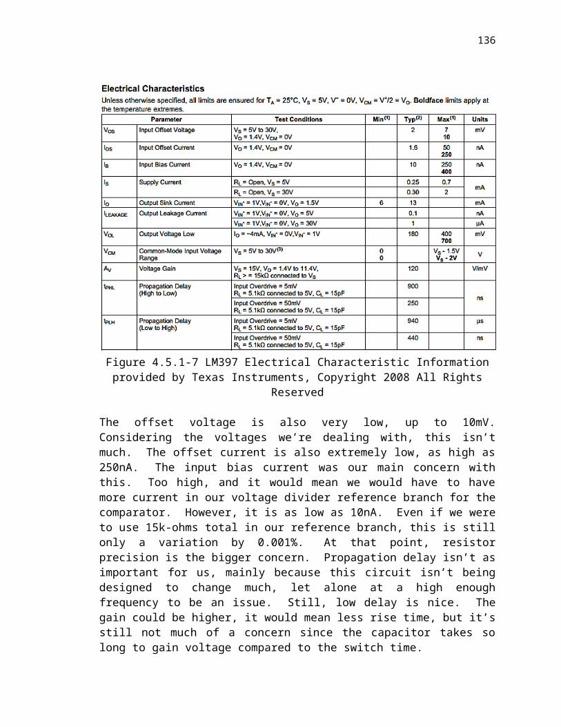
g
Appendix C: ReferencesSokal, Nathan O., and Alan D. Sokal. "Class E - A New Class of High-Efficiency Tuned Single-Ended Switching Power Amplifiers." IEEE Journal of Solid-State Circuits SC-10.3 (1975): 7. Print.
Murray, Charles. “Wireless Power Pitched as Replacement for EV Batteries”. DesignNews February 15, 2012. <http://www.designnews.com/author.asp?section_id=1366&doc_id=239008&dfpPParams=ind_184,industry_auto,bid_318,aid_239008&dfpLayout=blog>
Kim, Hyungrak. Lee, Hong-Min. “Design of an Integrated Wireless Power Transfer System with High Power Transfer Efficiency and Compact Structure” 6 th European Conference on Antennas and Propagation (EUCAP) July 12, 2011. IEEE Xplore Database.
Cheon, Sanghoon. Kim, Yong-Hae. Kang, Seung-Youl. Lee, Myung Lae. Lee, Jong-Moo. Zyung, Taehyoung. “Circuit-Model-Based Analysis of a Wireless Energy-Transfer System via Coupled Magnetic Resonances” IEEE Transactions on Industrial Electronics Vol. 58 No. 7. July 7, 2011. IEEE Xplore Database.