EECC551 - Shaaban #1 lec # 8 Fall 2004 10-14-2004 Main Memory Main memory generally utilizes Dynamic...
58
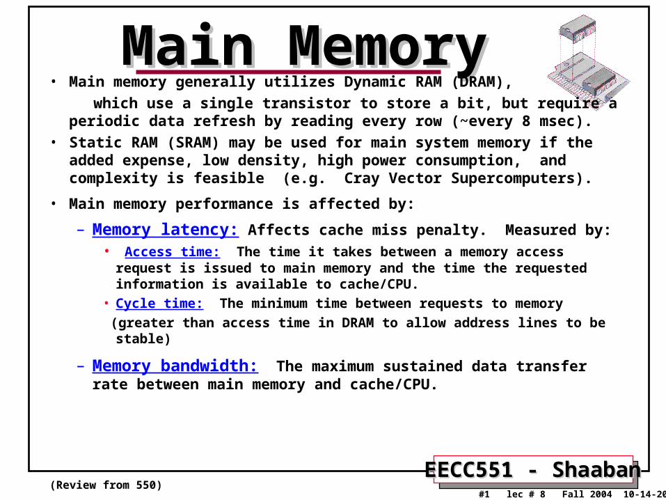
EECC551 - Shaaban EECC551 - Shaaban #1 lec # 8 Fall 2004 10-14-20 Main Memory Main Memory • Main memory generally utilizes Dynamic RAM (DRAM), which use a single transistor to store a bit, but require a periodic data refresh by reading every row (~every 8 msec). • Static RAM (SRAM) may be used for main system memory if the added expense, low density, high power consumption, and complexity is feasible (e.g. Cray Vector Supercomputers). • Main memory performance is affected by: – Memory latency: Affects cache miss penalty. Measured by: • Access time: The time it takes between a memory access request is issued to main memory and the time the requested information is available to cache/CPU. • Cycle time: The minimum time between requests to memory (greater than access time in DRAM to allow address lines to be stable) – Memory bandwidth: The maximum sustained data transfer rate between main memory and cache/CPU. (Review from 550)
-
date post
22-Dec-2015 -
Category
Documents
-
view
217 -
download
4
Transcript of EECC551 - Shaaban #1 lec # 8 Fall 2004 10-14-2004 Main Memory Main memory generally utilizes Dynamic...
EECC551 - ShaabanEECC551 - Shaaban#1 lec # 8 Fall 2004 10-14-2004
Main MemoryMain Memory• Main memory generally utilizes Dynamic RAM (DRAM),
which use a single transistor to store a bit, but require a periodic data refresh by reading every row (~every 8 msec).
• Static RAM (SRAM) may be used for main system memory if the added expense, low density, high power consumption, and complexity is feasible (e.g. Cray Vector Supercomputers).
• Main memory performance is affected by:
– Memory latency: Affects cache miss penalty. Measured by:• Access time: The time it takes between a memory access request is issued to
main memory and the time the requested information is available to cache/CPU.
• Cycle time: The minimum time between requests to memory
(greater than access time in DRAM to allow address lines to be stable)
– Memory bandwidth: The maximum sustained data transfer rate between main memory and cache/CPU.
(Review from 550)

EECC551 - ShaabanEECC551 - Shaaban#2 lec # 8 Fall 2004 10-14-2004
Logical DRAM Organization (16 Mbit)Logical DRAM Organization (16 Mbit)
Data In
Data Out
Column DecoderColumn Decoder
Sense Sense Amps & I/OAmps & I/O
Memory Memory ArrayArray(16,384 x 16,384)(16,384 x 16,384)
A0…A13A0…A130
…14DD
WWord Lineord Line Storage CellCell
Row
Dec
oder
Row
Dec
oder
Row/ColumnAddress
Control Signals:Row Access Strobe (RAS): Low to latch row addressColumn Address Strobe (CAS): Low to latch column addressWrite Enable (WE)Output Enable (OE)
(Review from 550)

EECC551 - ShaabanEECC551 - Shaaban#3 lec # 8 Fall 2004 10-14-2004
Key DRAM Speed Parameters• Row Access Strobe (RAS)Time:
– Minimum time from RAS (Row Access Strobe) line falling to the first valid data output.
– A major component of memory latency.– Only improves 5% every year.
• Column Access Strobe (CAS) Time/data transfer time:– The minimum time required to read additional data by changing column
address while keeping the same row address.– Along with memory bus width, determines peak memory bandwidth.
Example: for a memory with 8 bytes wide bus with RAS = 40 ns and CAS = 10 ns and the following simplified memory timing
(Review from 550)
RAS CAS CAS
1st 8 bytes
CAS CAS
2nd 8 bytes
3rd 8 bytes
4th 8 bytes
Memory Latency = RAS + CAS = 50 ns(to get first 8 bytes of data)
Peak Memory Bandwidth = Bus width / CAS = 8 x 100 x 106 = 800 Mbytes/s
Miss penalty to fill a cache with 32 byte block size = 80 ns (miss penalty)
40 ns 50 ns 60 ns 70 ns 80 ns
EECC551 - ShaabanEECC551 - Shaaban#4 lec # 8 Fall 2004 10-14-2004
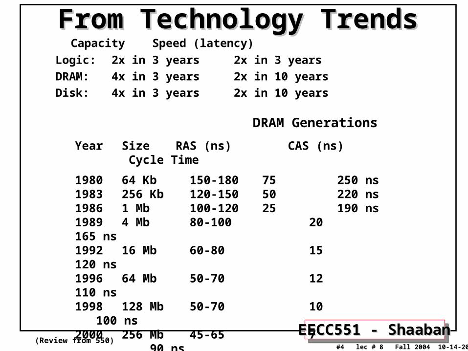
From Technology TrendsFrom Technology Trends Capacity Speed (latency)
Logic: 2x in 3 years 2x in 3 years
DRAM: 4x in 3 years 2x in 10 years
Disk: 4x in 3 years 2x in 10 years
DRAM Generations
Year Size RAS (ns) CAS (ns) Cycle Time
1980 64 Kb 150-180 75 250 ns1983 256 Kb 120-150 50 220 ns1986 1 Mb 100-120 25 190 ns1989 4 Mb 80-100 20 165 ns1992 16 Mb 60-80 15 120 ns1996 64 Mb 50-70 12 110 ns1998 128 Mb 50-70 10 100 ns2000 256 Mb 45-65 7 90 ns2002 512 Mb 40-60 5 80 ns
8000:1 15:1 3:1 (Capacity) (~bandwidth) (Latency)
(Review from 550)

EECC551 - ShaabanEECC551 - Shaaban#5 lec # 8 Fall 2004 10-14-2004
Memory Hierarchy: The motivationMemory Hierarchy: The motivation• The gap between CPU performance and main memory has been widening
with higher performance CPUs creating performance bottlenecks for memory access instructions.
• The memory hierarchy is organized into several levels of memory with the smaller, more expensive, and faster memory levels closer to the CPU: registers, then primary Cache Level (L1), then additional secondary cache levels (L2, L3…), then main memory, then mass storage (virtual memory).
• Each level of the hierarchy is a subset of the level below: data found in a level is also found in the level below (farther from CPU) but at lower speed.
• Each level maps addresses from a larger physical memory to a smaller level of physical memory closer to the CPU.
• This concept is greatly aided by the principal of locality both temporal and spatial which indicates that programs tend to reuse data and instructions that they have used recently or those stored in their vicinity leading to working set of a program.
(Review from 550)

EECC551 - ShaabanEECC551 - Shaaban#6 lec # 8 Fall 2004 10-14-2004
Memory Hierarchy: MotivationMemory Hierarchy: MotivationProcessor-Memory (DRAM) Performance GapProcessor-Memory (DRAM) Performance Gap
µProc60%/yr.
DRAM7%/yr.
1
10
100
1000198
0198
1 198
3198
4198
5 198
6198
7198
8198
9199
0199
1 199
2199
3199
4199
5199
6199
7199
8 199
9200
0
DRAM
CPU
198
2
Processor-MemoryPerformance Gap:(grows 50% / year)
Per
form
ance
(Review from 550)
EECC551 - ShaabanEECC551 - Shaaban#7 lec # 8 Fall 2004 10-14-2004
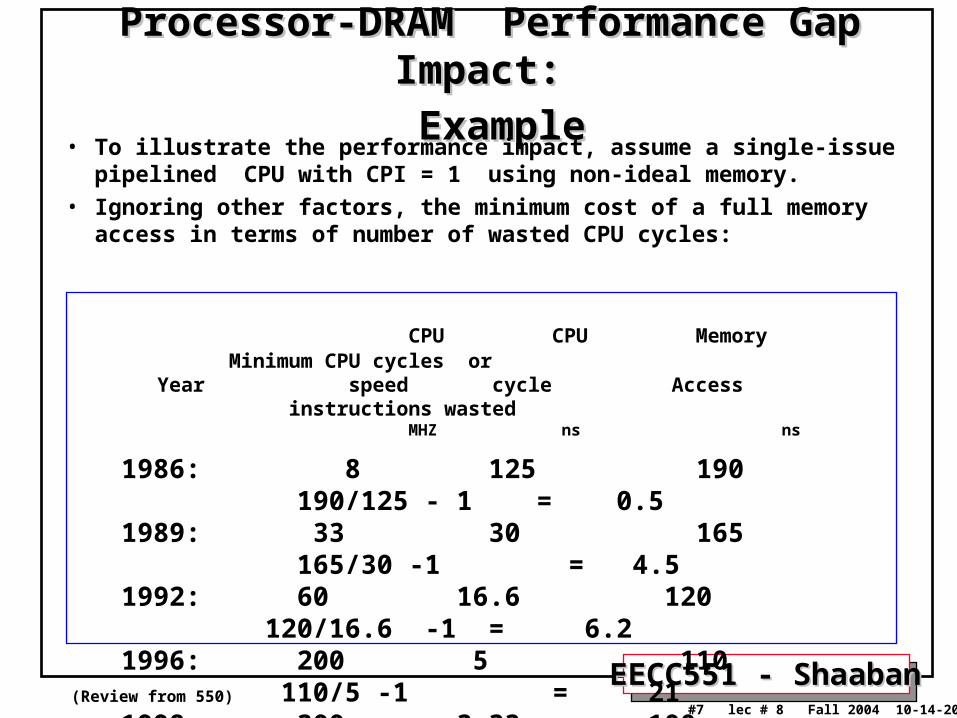
Processor-DRAM Performance Gap Impact: Processor-DRAM Performance Gap Impact:
Example Example• To illustrate the performance impact, assume a single-issue pipelined CPU
with CPI = 1 using non-ideal memory. • Ignoring other factors, the minimum cost of a full memory access in terms of
number of wasted CPU cycles:
CPU CPU Memory Minimum CPU cycles or Year speed cycle Access instructions wasted MHZ ns ns
1986: 8 125 190 190/125 - 1 = 0.51989: 33 30 165 165/30 -1 = 4.51992: 60 16.6 120 120/16.6 -1 = 6.21996: 200 5 110 110/5 -1 = 211998: 300 3.33 100 100/3.33 -1 = 292000: 1000 1 90 90/1 - 1 = 892002: 2000 .5 80 80/.5 - 1 = 159
(Review from 550)

EECC551 - ShaabanEECC551 - Shaaban#8 lec # 8 Fall 2004 10-14-2004
Memory Hierarchy: MotivationMemory Hierarchy: Motivation
The Principle Of LocalityThe Principle Of Locality• Programs usually access a relatively small portion of their address
space (instructions/data) at any instant of time (program working set).
• Two Types of locality:
– Temporal Locality: If an item is referenced, it will tend to be referenced again soon.
– Spatial locality: If an item is referenced, items whose addresses are close will tend to be referenced soon.
• The presence of locality in program behavior, makes it possible to satisfy a large percentage of program access needs (both instructions and operands) using memory levels with much less capacity than program address space.
(Review from 550)

EECC551 - ShaabanEECC551 - Shaaban#9 lec # 8 Fall 2004 10-14-2004
Levels of The Memory HierarchyLevels of The Memory Hierarchy
Part of The On-chip CPU Datapath 16-256 Registers
One or more levels (Static RAM):Level 1: On-chip 16-64K Level 2: On-chip 256K-2MLevel 3: On or Off-chip 1M-16M
Registers
CacheLevel(s)
Main Memory
Magnetic Disc
Optical Disk or Magnetic Tape
Farther away from the CPU:
Lower Cost/Bit
Higher Capacity
Increased AccessTime/Latency
Lower Throughput/Bandwidth
DRAM, RDRAM 256M-16G
Interface:SCSI, RAID, IDE, 139480G-300G
(Review from 550)
CPU

EECC551 - ShaabanEECC551 - Shaaban#10 lec # 8 Fall 2004 10-14-2004
Memory Hierarchy OperationMemory Hierarchy Operation• If an instruction or operand is required by the CPU, the levels of the
memory hierarchy are searched for the item starting with the level closest to the CPU (Level 1 cache):– If the item is found, it’s delivered to the CPU resulting in a cache hit
without searching lower levels.– If the item is missing from an upper level, resulting in a miss, the level
just below is searched. – For systems with several levels of cache, the search continues with
cache level 2, 3 etc.– If all levels of cache report a miss then main memory is accessed for
the item.• CPU cache memory: Managed by hardware.
– If the item is not found in main memory resulting in a page fault, then disk (virtual memory), is accessed for the item.• Memory disk: Managed by the operating system with
hardware support
(Review from 550)

EECC551 - ShaabanEECC551 - Shaaban#11 lec # 8 Fall 2004 10-14-2004
Memory Hierarchy: TerminologyMemory Hierarchy: Terminology• A Block: The smallest unit of information transferred between two
levels.
• Hit: Item is found in some block in the upper level (example: Block X)
– Hit Rate: The fraction of memory access found in the upper level.
– Hit Time: Time to access the upper level which consists of
RAM access time + Time to determine hit/miss
• Miss: Item needs to be retrieved from a block in the lower level (Block Y)
– Miss Rate = 1 - (Hit Rate)
– Miss Penalty: Time to replace a block in the upper level +
Time to deliver the missed block to the processor
• Hit Time << Miss Penalty
Lower LevelMemoryUpper Level
MemoryTo Processor
From ProcessorBlk X
Blk Y
(Review from 550)
e.g cache
e.g main memory

EECC551 - ShaabanEECC551 - Shaaban#12 lec # 8 Fall 2004 10-14-2004
Basic Cache ConceptsBasic Cache Concepts• Cache is the first level of the memory hierarchy once the address leaves
the CPU and is searched first for the requested data.
• If the data requested by the CPU is present in the cache, it is retrieved from cache and the data access is a cache hit otherwise a cache miss and data must be read from main memory.
• On a cache miss a block of data must be brought in from main memory to cache to possibly replace an existing cache block.
• The allowed block addresses where blocks can be mapped (placed) into cache from main memory is determined by cache placement strategy.
• Locating a block of data in cache is handled by cache block identification mechanism.
• On a cache miss choosing the cache block being removed (replaced) is handled by the block replacement strategy in place.
• When a write to cache is requested, a number of main memory update strategies exist as part of the cache write policy.
(Review from 550)

EECC551 - ShaabanEECC551 - Shaaban#13 lec # 8 Fall 2004 10-14-2004
Cache Design & Operation IssuesCache Design & Operation Issues• Q1: Where can a block be placed cache?
(Block placement strategy & Cache organization)– Fully Associative, Set Associative, Direct Mapped.
• Q2: How is a block found if it is in cache? (Block identification)– Tag/Block.
• Q3: Which block should be replaced on a miss? (Block replacement)– Random, LRU.
• Q4: What happens on a write? (Cache write policy)– Write through, write back.
(Review from 550)
EECC551 - ShaabanEECC551 - Shaaban#14 lec # 8 Fall 2004 10-14-2004
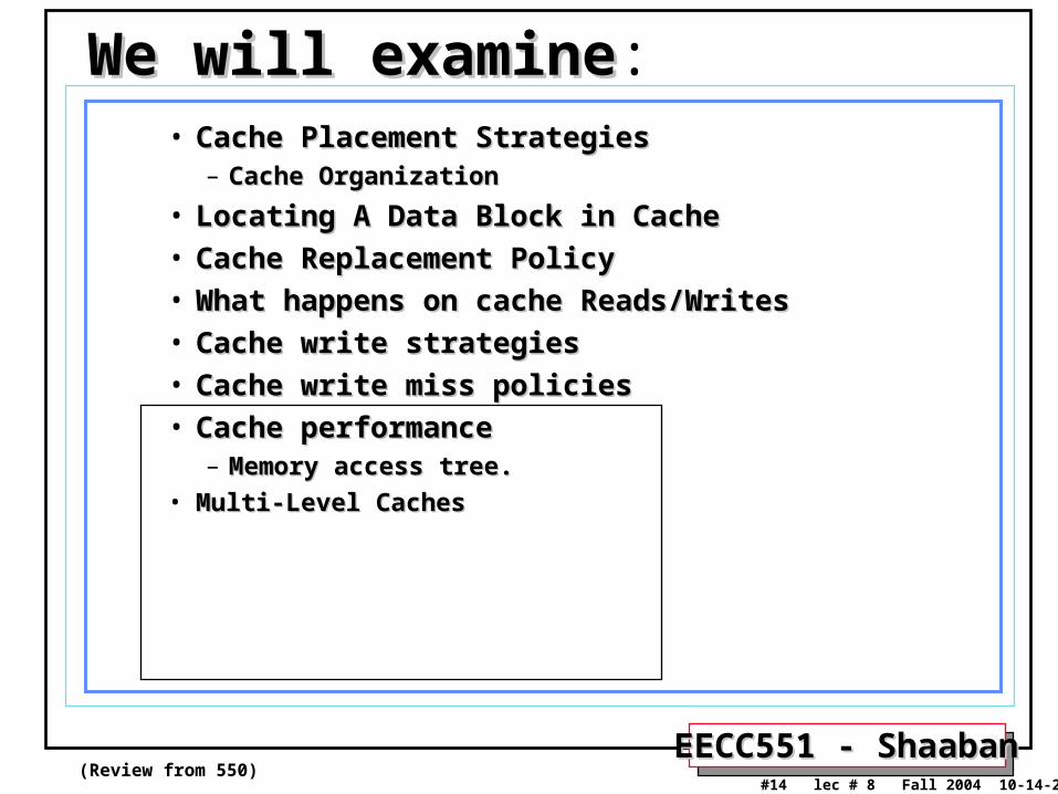
We will examineWe will examine:• Cache Placement StrategiesCache Placement Strategies
– Cache OrganizationCache Organization
• Locating A Data Block in CacheLocating A Data Block in Cache• Cache Replacement PolicyCache Replacement Policy• What happens on cache Reads/WritesWhat happens on cache Reads/Writes• Cache write strategiesCache write strategies• Cache write miss policiesCache write miss policies• Cache performanceCache performance
– Memory access tree.Memory access tree.• Multi-Level CachesMulti-Level Caches
(Review from 550)

EECC551 - ShaabanEECC551 - Shaaban#15 lec # 8 Fall 2004 10-14-2004
Cache Organization & Placement StrategiesCache Organization & Placement StrategiesPlacement strategies or mapping of a main memory data block onto
cache block frame addresses divide cache into three organizations:
1 Direct mapped cache: A block can be placed in only one location (cache block frame), given by the mapping function:
index= (Block address) MOD (Number of blocks in cache)
2 Fully associative cache: A block can be placed anywhere in cache. (no mapping function).
3 Set associative cache: A block can be placed in a restricted set of places, or cache block frames. A set is a group of block frames in the cache. A block is first mapped onto the set and then it can be placed anywhere within the set. The set in this case is chosen by:
index = (Block address) MOD (Number of sets in cache)
If there are n blocks in a set the cache placement is called n-way set-associative.
(Review from 550)

EECC551 - ShaabanEECC551 - Shaaban#16 lec # 8 Fall 2004 10-14-2004
Cache Organization: Cache Organization: Direct Mapped CacheDirect Mapped Cache
0 0 0 0 1 0 0 1 0 1 0 1 0 0 1 0 1 1 0 1 1 0 0 0 1 1 0 1 0 1 1 1 0 0 1 1 1 1 0 1
00
0
C a c h e
M e m o ry
00
1
01
0
01
1
10
0
10
1
11
0
11
1
A block can be placed in one location only, given by: (Block address) MOD (Number of blocks in cache) In this case, mapping function: (Block address) MOD (8)
32 memory blockscacheable
8 cache block frames
(i.e low three bits of block address)
Example: 29 MOD 8 = 5(11101) MOD (1000) = 101
(Review from 550)
Index bits

EECC551 - ShaabanEECC551 - Shaaban#17 lec # 8 Fall 2004 10-14-2004
4KB Direct Mapped 4KB Direct Mapped Cache ExampleCache Example
A d d re s s ( s h o w in g b it p o s i t io n s )
2 0 1 0
B y te
o ffs e t
V a l id T a g D a taIn d e x
0
1
2
1 0 2 1
1 0 2 2
1 0 2 3
T a g
In d e x
H i t D a ta
2 0 3 2
3 1 3 0 1 3 1 2 1 1 2 1 0
1K = 1024 BlocksEach block = one word
Can cache up to232 bytes = 4 GBof memory
Mapping function:
Cache Block frame number =(Block address) MOD (1024)
i.e. index field or 10 low bit of block address
Index fieldTag field
Block offset = 2 bits
Block Address = 30 bits
Tag = 20 bits Index = 10 bits
(Review from 550)

EECC551 - ShaabanEECC551 - Shaaban#18 lec # 8 Fall 2004 10-14-2004
64KB Direct Mapped Cache Example64KB Direct Mapped Cache ExampleA d d re s s (s ho w in g b it p o s ition s)
1 6 1 2 B yte
o ffs e t
V T a g D a ta
H it D a ta
1 6 32
4 K
e n tr ie s
1 6 b its 12 8 b i ts
M u x
3 2 3 2 3 2
2
3 2
B lo c k o f fs e tIn d ex
T ag
3 1 16 1 5 4 3 2 1 04K= 4096 blocksEach block = four words = 16 bytes
Can cache up to232 bytes = 4 GBof memory
Mapping Function: Cache Block frame number = (Block address) MOD (4096) i.e. index field or 12 low bit of block address
Index fieldTag field
Word select
Block Address = 28 bits
Tag = 16 bits Index = 12 bits Block offset = 4 bits
Larger cache blocks take better advantage of spatial locality
(Review from 550)
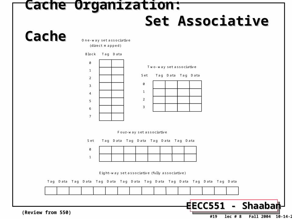
EECC551 - ShaabanEECC551 - Shaaban#19 lec # 8 Fall 2004 10-14-2004
T a g D a ta T a g D a ta T a g D a ta T a g D a ta T a g D a ta T a g D a ta T a g D a ta T a g D a ta
E ig h t - w a y s e t a s s o c ia t iv e ( fu l ly a s s o c ia t iv e )
T a g D a t a T a g D a ta T a g D a ta T a g D a ta
F o u r - w a y s e t a s s o c ia t iv e
S e t
0
1
T a g D a t a
O n e - w a y s e t a s s o c ia t iv e
(d i re c t m a p p e d )
B lo c k
0
7
1
2
3
4
5
6
T a g D a ta
T w o - w a y s e t a s s o c ia t iv e
S e t
0
1
2
3
T a g D a ta
Cache Organization: Cache Organization: Set Associative CacheSet Associative Cache
(Review from 550)

EECC551 - ShaabanEECC551 - Shaaban#20 lec # 8 Fall 2004 10-14-2004
Cache Organization/Mapping ExampleCache Organization/Mapping Example
(Review from 550)
8 Block Frames
32 Block Frames

EECC551 - ShaabanEECC551 - Shaaban#21 lec # 8 Fall 2004 10-14-2004
Locating A Data Block in CacheLocating A Data Block in Cache• Each block frame in cache has an address tag.
• The tags of every cache block that might contain the required data are checked in parallel.
• A valid bit is added to the tag to indicate whether this entry contains a valid address.
• The address from the CPU to cache is divided into:
– A block address, further divided into:
• An index field to choose a block set in cache.
(no index field when fully associative).
• A tag field to search and match addresses in the selected set.
– A block offset to select the data from the block.
Block Address BlockOffsetTag Index
(Review from 550)

EECC551 - ShaabanEECC551 - Shaaban#22 lec # 8 Fall 2004 10-14-2004
Address Field Sizes/MappingAddress Field Sizes/Mapping
Block Address BlockOffsetTag Index
Block offset size = log2(block size)
Index size = log2(Total number of blocks/associativity)
Tag size = address size - index size - offset sizeTag size = address size - index size - offset size
Physical Memory Address Generated by CPU
Mapping function:
Cache set or block frame number = Index = = (Block Address) MOD (Number of Sets)
Number of Sets in cache
(Review from 550)
No index/mapping function for fully associative cache
(size determined by amount of physical main memory cacheable)

EECC551 - ShaabanEECC551 - Shaaban#23 lec # 8 Fall 2004 10-14-2004
4K Four-Way Set Associative Cache:4K Four-Way Set Associative Cache:MIPS Implementation ExampleMIPS Implementation Example
Ad dress
2 2 8
V TagIndex
0
1
2
253
254
255
D ata V Tag D ata V Tag D ata V Tag D ata
3 22 2
4 - to - 1 m ultip lexo r
H it D a ta
123891011123 031 0
IndexField
TagField
1024 block framesEach block = one word4-way set associative1024 / 4= 256 sets
Can cache up to232 bytes = 4 GBof memory
Block Address = 30 bits
Tag = 22 bits Index = 8 bits Block offset = 2 bits
Mapping Function: Cache Set Number = index= (Block address) MOD (256)
(Review from 550)
BlockOffset

EECC551 - ShaabanEECC551 - Shaaban#24 lec # 8 Fall 2004 10-14-2004
Cache Replacement PolicyCache Replacement Policy• When a cache miss occurs the cache controller may have to select a block of
cache data to be removed from a cache block frame and replaced with the requested data, such a block is selected by one of three methods:
(No cache replacement policy in direct mapped cache)
– Random: • Any block is randomly selected for replacement providing uniform
allocation.
• Simple to build in hardware. Most widely used cache replacement strategy.
– Least-recently used (LRU): • Accesses to blocks are recorded and and the block replaced is the one
that was not used for the longest period of time.• Full LRU is expensive to implement, as the number of blocks to be
tracked increases, and is usually approximated by block usage bits that are cleared at regular time intervals.
– First In, First Out (FIFO: • Because LRU can be complicated to implement, this approximates LRU
by determining the oldest block rather than LRU
(Review from 550)

EECC551 - ShaabanEECC551 - Shaaban#25 lec # 8 Fall 2004 10-14-2004
Miss Rates for Caches with Different Size, Miss Rates for Caches with Different Size, Associativity & Replacement AlgorithmAssociativity & Replacement Algorithm
Sample DataSample Data
Associativity: 2-way 4-way 8-way
Size LRU Random LRU Random LRURandom
16 KB 5.18% 5.69% 4.67% 5.29% 4.39% 4.96%
64 KB 1.88% 2.01% 1.54% 1.66% 1.39% 1.53%
256 KB 1.15% 1.17% 1.13% 1.13% 1.12% 1.12%
(Review from 550)
FIFO replacement miss rates (not shown here) is better than random but worse than LRU
EECC551 - ShaabanEECC551 - Shaaban#26 lec # 8 Fall 2004 10-14-2004
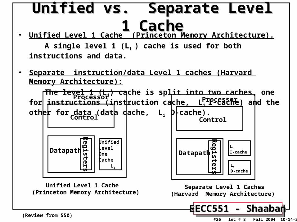
Unified vs. Separate Level 1 CacheUnified vs. Separate Level 1 Cache• Unified Level 1 Cache (Princeton Memory Architecture).
A single level 1 (L1 ) cache is used for both instructions and data.
• Separate instruction/data Level 1 caches (Harvard Memory Architecture):
The level 1 (L1) cache is split into two caches, one for instructions (instruction cache, L1 I-cache) and the other for data (data cache, L1 D-cache).
Control
Datapath
Processor
Registers
UnifiedLevel OneCache L1
Control
Datapath
Processor
Registers
L1
I-cache
L1
D-cache
Unified Level 1 Cache (Princeton Memory Architecture)
Separate Level 1 Caches (Harvard Memory Architecture)
(Review from 550)

EECC551 - ShaabanEECC551 - Shaaban#27 lec # 8 Fall 2004 10-14-2004
Cache Performance:Average Memory Access Time (AMAT), Memory Stall cycles
• The Average Memory Access Time (AMAT): The number of cycles required to complete an average memory access request by the CPU.
• Memory stall cycles per memory access: The number of stall cycles added to CPU execution cycles for one memory access.
• For ideal memory: AMAT = 1 cycle, this results in zero memory stall cycles.
• Memory stall cycles per average memory access = (AMAT -1)
• Memory stall cycles per average instruction =
Memory stall cycles per average memory access
x Number of memory accesses per instruction
= (AMAT -1 ) x ( 1 + fraction of loads/stores)
Instruction Fetch
EECC551 - ShaabanEECC551 - Shaaban#28 lec # 8 Fall 2004 10-14-2004
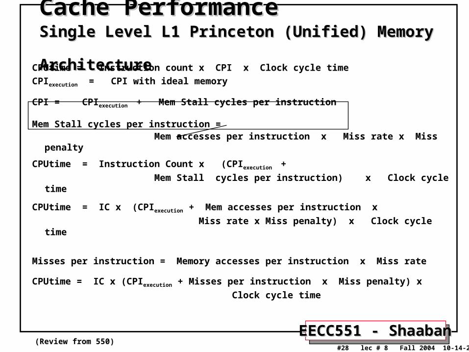
Cache PerformanceCache Performance Single Level L1 Princeton (Unified) Memory ArchitectureSingle Level L1 Princeton (Unified) Memory Architecture
CPUtime = Instruction count x CPI x Clock cycle time
CPIexecution = CPI with ideal memory
CPI = CPIexecution + Mem Stall cycles per instruction
Mem Stall cycles per instruction = Mem accesses per instruction x Miss rate x Miss penalty
CPUtime = Instruction Count x (CPIexecution +
Mem Stall cycles per instruction) x Clock cycle time
CPUtime = IC x (CPIexecution + Mem accesses per instruction x
Miss rate x Miss penalty) x Clock cycle time
Misses per instruction = Memory accesses per instruction x Miss rate
CPUtime = IC x (CPIexecution + Misses per instruction x Miss penalty) x
Clock cycle time
(Review from 550)

EECC551 - ShaabanEECC551 - Shaaban#29 lec # 8 Fall 2004 10-14-2004
Memory Access TreeFor Unified Level 1 Cache
CPU Memory Access
L1 Miss: % = (1- Hit rate) = (1-H1) Access time = M + 1 Stall cycles per access = M x (1-H1)
L1 Hit: % = Hit Rate = H1 Access Time = 1Stalls= H1 x 0 = 0 ( No Stall)
L1
AMAT = H1 x 1 + (1 -H1 ) x (M+ 1) = 1 + M x ( 1 -H1)
Stall Cycles Per Access = AMAT - 1 = M x (1 -H1)CPI = CPIexecution + Mem accesses per instruction x M x (1 -H1)
M = Miss PenaltyH1 = Level 1 Hit Rate1- H1 = Level 1 Miss Rate

EECC551 - ShaabanEECC551 - Shaaban#30 lec # 8 Fall 2004 10-14-2004
Cache Impact On Performance: Cache Impact On Performance: An ExampleAn Example
Assuming the following execution and cache parameters:– Cache miss penalty = 50 cycles
– Normal instruction execution CPI ignoring memory stalls = 2.0 cycles
– Miss rate = 2%
– Average memory references/instruction = 1.33
CPU time = IC x [CPI execution + Memory accesses/instruction x Miss rate x
Miss penalty ] x Clock cycle time
CPUtime with cache = IC x (2.0 + (1.33 x 2% x 50)) x clock cycle time
= IC x 3.33 x Clock cycle time
Lower CPI execution increases the impact of cache miss clock cycles

EECC551 - ShaabanEECC551 - Shaaban#31 lec # 8 Fall 2004 10-14-2004
Cache Performance ExampleCache Performance Example• Suppose a CPU executes at Clock Rate = 200 MHz (5 ns per cycle) with a
single level of cache.
• CPIexecution = 1.1
• Instruction mix: 50% arith/logic, 30% load/store, 20% control• Assume a cache miss rate of 1.5% and a miss penalty of 50 cycles.
CPI = CPIexecution + mem stalls per instruction
Mem Stalls per instruction =
Mem accesses per instruction x Miss rate x Miss penalty
Mem accesses per instruction = 1 + .3 = 1.3
Mem Stalls per instruction = 1.3 x .015 x 50 = 0.975
CPI = 1.1 + .975 = 2.075
The ideal memory CPU with no misses is 2.075/1.1 = 1.88 times faster
Instruction fetch Load/store

EECC551 - ShaabanEECC551 - Shaaban#32 lec # 8 Fall 2004 10-14-2004
Cache Performance ExampleCache Performance Example• Suppose for the previous example we double the clock rate to
400 MHZ, how much faster is this machine, assuming similar miss rate, instruction mix?
• Since memory speed is not changed, the miss penalty takes more CPU cycles:
Miss penalty = 50 x 2 = 100 cycles.
CPI = 1.1 + 1.3 x .015 x 100 = 1.1 + 1.95 = 3.05
Speedup = (CPIold x Cold)/ (CPInew x Cnew)
= 2.075 x 2 / 3.05 = 1.36
The new machine is only 1.36 times faster rather than 2 times faster due to the increased effect of cache misses.
CPUs with higher clock rate, have more cycles per cache miss and more
memory impact on CPI.

EECC551 - ShaabanEECC551 - Shaaban#33 lec # 8 Fall 2004 10-14-2004
Cache PerformanceCache PerformanceHarvard Memory ArchitectureHarvard Memory Architecture
For a CPU with separate or split level one (L1) caches for
instructions and data (Harvard memory architecture) and no stalls
for cache hits: CPUtime = Instruction count x CPI x Clock cycle time
CPI = CPIexecution + Mem Stall cycles per instruction
CPUtime = Instruction Count x (CPIexecution +
Mem Stall cycles per instruction) x Clock cycle time
Mem Stall cycles per instruction = Instruction Fetch Miss rate x Miss Penalty + Data Memory Accesses Per Instruction x Data Miss Rate x Miss Penalty

EECC551 - ShaabanEECC551 - Shaaban#34 lec # 8 Fall 2004 10-14-2004
Memory Access TreeFor Separate Level 1 Caches
CPU Memory Access
L1
Instruction Data
Data L1 Miss:Access Time : M + 1Stalls per access: % data x (1 - Data H1 ) x M
Data L1 Hit:Access Time: 1 Stalls = 0
Instruction L1 Hit:Access Time = 1Stalls = 0
Instruction L1 Miss:Access Time = M + 1Stalls Per access
%instructions x (1 - Instruction H1 ) x M
Stall Cycles Per Access = % Instructions x ( 1 - Instruction H1 ) x M + % data x (1 - Data H1 ) x M
AMAT = 1 + Stall Cycles per access

EECC551 - ShaabanEECC551 - Shaaban#35 lec # 8 Fall 2004 10-14-2004
Cache Performance ExampleCache Performance Example• Suppose a CPU uses separate level one (L1) caches for instructions and data (Harvard memory
architecture) with different miss rates for instruction and data access:
– A cache hit incurs no stall cycles while a cache miss incurs 200 stall cycles for both memory reads and writes.
– CPIexecution = 1.1
– Instruction mix: 50% arith/logic, 30% load/store, 20% control– Assume a cache miss rate of 0.5% for instruction fetch and a cache data miss rate of 6%. – A cache hit incurs no stall cycles while a cache miss incurs 200 stall cycles for both memory reads and
writes. Find the resulting CPI using this cache? How much faster is the CPU with ideal memory?
CPI = CPIexecution + mem stalls per instruction
Mem Stall cycles per instruction = Instruction Fetch Miss rate x Miss Penalty +
Data Memory Accesses Per Instruction x Data Miss Rate x Miss Penalty
Mem Stall cycles per instruction = 0.5/100 x 200 + 0.3 x 6/100 x 200 = 1 + 3.6 = 4.6
CPI = CPIexecution + mem stalls per instruction = 1.1 + 4.6 = 5.7
The CPU with ideal cache (no misses) is 5.7/1.1 = 5.18 times faster
With no cache the CPI would have been = 1.1 + 1.3 X 200 = 261.1 !!

EECC551 - ShaabanEECC551 - Shaaban#36 lec # 8 Fall 2004 10-14-2004
Typical Cache Performance DataTypical Cache Performance Data Using SPEC92Using SPEC92

EECC551 - ShaabanEECC551 - Shaaban#37 lec # 8 Fall 2004 10-14-2004
Cache Read/Write OperationsCache Read/Write Operations• Statistical data suggest that reads (including instruction fetches)
dominate processor cache accesses (writes account for ~ 25% of data cache traffic).
• In cache reads, a block is read at the same time while the tag is being compared with the block address. If the read is a hit the data is passed to the CPU, if a miss it ignores it.
• In cache writes, modifying the block cannot begin until the tag is checked to see if the address is a hit.
• Thus for cache writes, tag checking cannot take place in parallel, and only the specific data (between 1 and 8 bytes) requested by the CPU can be modified.
• Cache can be classified according to the write and memory update strategy in place: write through, or write back.

EECC551 - ShaabanEECC551 - Shaaban#38 lec # 8 Fall 2004 10-14-2004
Cache Write StrategiesCache Write Strategies1 Write Though: Data is written to both the cache block and to a
block of main memory.
– The lower level always has the most updated data; an important feature for I/O and multiprocessing.
– Easier to implement than write back.
– A write buffer is often used to reduce CPU write stall while data is written to memory.
2 Write back: Data is written or updated only to the cache block. The modified or dirty cache block is written to main memory when it’s being replaced from cache.
– Writes occur at the speed of cache– A status bit called a dirty or modified bit, is used to indicate
whether the block was modified while in cache; if not the block is not written back to main memory when replaced.
– Advantage: Uses less memory bandwidth than write through.

EECC551 - ShaabanEECC551 - Shaaban#39 lec # 8 Fall 2004 10-14-2004
Cache Write Strategies:Cache Write Strategies:
Write ThroughWrite Hit Operation (block to be written to is in cache)
Cache Memory
Write(Store)
Write to cache Without Write Buffer:Write to cache and also to memory
Write Penalty =M
Write Buffer
With perfect write buffer:Write to cache and also to write buffer
No penalty (no stall)
For cache write miss:With no write allocate Similar but no write to cachePenalty is still M
Write Back Cache Memory
Write(Store)
Write to cache
No write to memory
Just write to cache blockand set dirty or modified bit to 1
No penalty (no stall)
1 Set modified/dirty bit to 1 to indicatethat cache block has been modified (i.e block is dirty)

EECC551 - ShaabanEECC551 - Shaaban#40 lec # 8 Fall 2004 10-14-2004
Cache Write Miss PolicyCache Write Miss Policy• Since data is usually not needed immediately on a write miss
two options exist on a cache write miss:
Write Allocate:
The cache block is loaded on a write miss followed by write hit actions.
No-Write Allocate:
The block is modified in the lower level (lower cache level, or main
memory) and not loaded into cache.
While any of the above two write miss policies can be used with either write back or write through:
• Write back caches always use write allocate to capture subsequent writes to the block in cache.
• Write through caches usually use no-write allocate since subsequent writes still have to go to memory.

EECC551 - ShaabanEECC551 - Shaaban#41 lec # 8 Fall 2004 10-14-2004
CPU readsor writes to block in cache
Block to be replaced is clean
Write Back Cache With Write Allocate: Cache Miss Operation
Cache Memory
1
Cache Memory
0
Set modified/dirty bit to 1 if this is a write
Read missed block from memory
Penalty =M
1
2CPU readsor writes to block in cache
Block to be replaced is dirty
Replaced (old)block is discarded since it’s clean
Write replaced modified block to memory
Penalty =M
1
Read missed block from memory
Penalty =M
2
Set modified/dirty bit to 1 if this is a write
3
1 Write replaced modified block to memory
Penalty =M2 Read missed block from memory
Penalty =M
Total Miss Penalty = M + M = 2M
Miss Penalty = M

EECC551 - ShaabanEECC551 - Shaaban#42 lec # 8 Fall 2004 10-14-2004
Memory Access Tree, Unified L1
Write Through, No Write Allocate, No Write Buffer
CPU Memory Access
L1
Read Write
L1 Write Miss:Access Time : M + 1Stalls per access: % write x (1 - H1 ) x M
L1 Write Hit:Access Time: M +1 Stalls Per access:% write x (H1 ) x M
L1 Read Hit:Access Time = 1Stalls = 0
L1 Read Miss:Access Time = M + 1Stalls Per access
% reads x (1 - H1 ) x M
Stall Cycles Per Memory Access = % reads x (1 - H1 ) x M + % write x M
AMAT = 1 + % reads x (1 - H1 ) x M + % write x M M = Miss PenaltyH1 = Level 1 Hit Rate1- H1 = Level 1 Miss Rate

EECC551 - ShaabanEECC551 - Shaaban#43 lec # 8 Fall 2004 10-14-2004
• To reduce write stalls when write though is used, a write buffer is used to eliminate or reduce write stalls:
– Perfect write buffer: All writes are handled by write buffer, no stalling for writes
– In this case (for unified L1 cache):
Stall Cycles Per Memory Access = % reads x (1 - H1 ) x M
(i.e No stalls at all for writes)
– Realistic Write buffer: A percentage of write stalls are not eliminated when the write buffer is full.
– In this case (for unified L1 cache): Stall Cycles/Memory Access = ( % reads x (1 - H1 ) + % write stalls not eliminated ) x M
Reducing Write Stalls For Write Though CacheWrite Buffers
EECC551 - ShaabanEECC551 - Shaaban#44 lec # 8 Fall 2004 10-14-2004
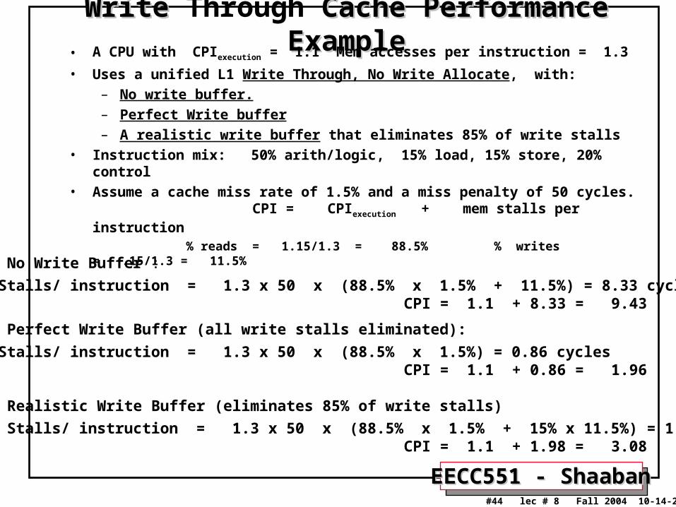
Write Write Through Cache Performance Example Cache Performance Example• A CPU with CPIexecution = 1.1 Mem accesses per instruction = 1.3
• Uses a unified L1 Write Through, No Write Allocate, with:
– No write buffer.
– Perfect Write buffer
– A realistic write buffer that eliminates 85% of write stalls
• Instruction mix: 50% arith/logic, 15% load, 15% store, 20% control
• Assume a cache miss rate of 1.5% and a miss penalty of 50 cycles. CPI = CPIexecution + mem stalls per instruction
% reads = 1.15/1.3 = 88.5% % writes = .15/1.3 = 11.5%
With No Write Buffer :
Mem Stalls/ instruction = 1.3 x 50 x (88.5% x 1.5% + 11.5%) = 8.33 cycles CPI = 1.1 + 8.33 = 9.43
With Perfect Write Buffer (all write stalls eliminated):
Mem Stalls/ instruction = 1.3 x 50 x (88.5% x 1.5%) = 0.86 cycles CPI = 1.1 + 0.86 = 1.96
With Realistic Write Buffer (eliminates 85% of write stalls)
Mem Stalls/ instruction = 1.3 x 50 x (88.5% x 1.5% + 15% x 11.5%) = 1.98 cycles CPI = 1.1 + 1.98 = 3.08
EECC551 - ShaabanEECC551 - Shaaban#45 lec # 8 Fall 2004 10-14-2004
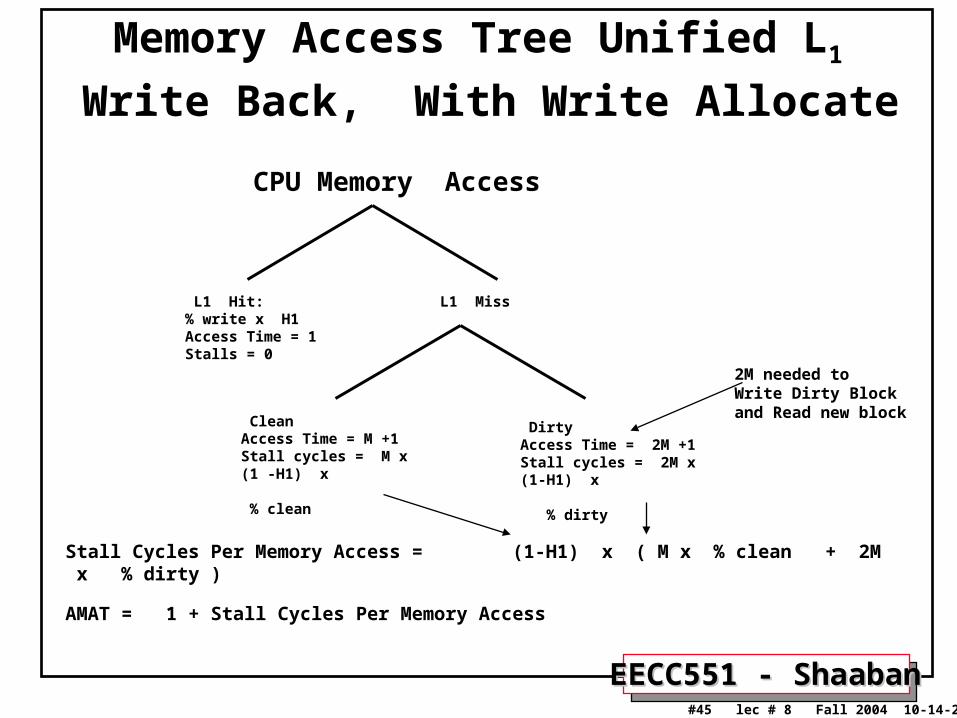
Memory Access Tree Unified L1
Write Back, With Write Allocate
CPU Memory Access
L1 Miss L1 Hit:% write x H1Access Time = 1Stalls = 0
Stall Cycles Per Memory Access = (1-H1) x ( M x % clean + 2M x % dirty )
AMAT = 1 + Stall Cycles Per Memory Access
CleanAccess Time = M +1Stall cycles = M x (1 -H1) x % clean
DirtyAccess Time = 2M +1Stall cycles = 2M x (1-H1) x % dirty
2M needed toWrite Dirty Blockand Read new block
EECC551 - ShaabanEECC551 - Shaaban#46 lec # 8 Fall 2004 10-14-2004
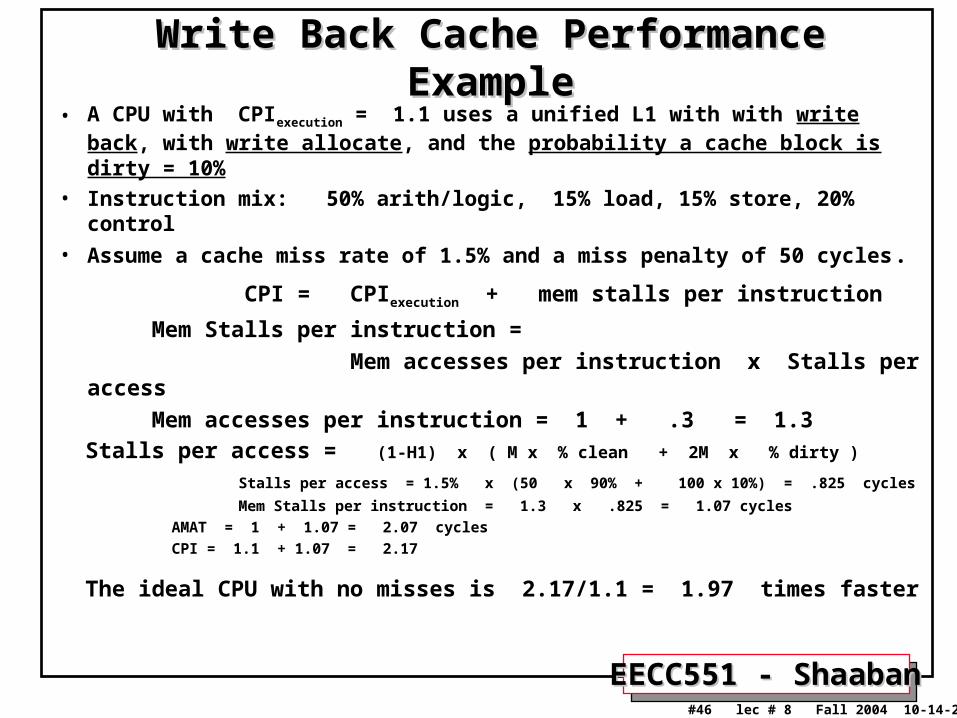
Write Back Cache Performance ExampleWrite Back Cache Performance Example• A CPU with CPIexecution = 1.1 uses a unified L1 with with write back, with
write allocate, and the probability a cache block is dirty = 10% • Instruction mix: 50% arith/logic, 15% load, 15% store, 20% control
• Assume a cache miss rate of 1.5% and a miss penalty of 50 cycles.
CPI = CPIexecution + mem stalls per instruction
Mem Stalls per instruction =
Mem accesses per instruction x Stalls per access
Mem accesses per instruction = 1 + .3 = 1.3
Stalls per access = (1-H1) x ( M x % clean + 2M x % dirty )
Stalls per access = 1.5% x (50 x 90% + 100 x 10%) = .825 cycles
Mem Stalls per instruction = 1.3 x .825 = 1.07 cycles
AMAT = 1 + 1.07 = 2.07 cycles
CPI = 1.1 + 1.07 = 2.17
The ideal CPU with no misses is 2.17/1.1 = 1.97 times faster

EECC551 - ShaabanEECC551 - Shaaban#47 lec # 8 Fall 2004 10-14-2004
2 Levels of Cache: L2 Levels of Cache: L11, L, L22
CPU
L1 Cache
L2 Cache
Main Memory
Hit Rate= H1, Hit time = 1 cycle (No Stall)
Hit Rate= H2, Hit time = T2 cycles
Memory access penalty, M

EECC551 - ShaabanEECC551 - Shaaban#48 lec # 8 Fall 2004 10-14-2004
Miss Rates For Multi-Level CachesMiss Rates For Multi-Level Caches• Local Miss Rate: This rate is the number of misses in a
cache level divided by the number of memory accesses to this level. Local Hit Rate = 1 - Local Miss Rate
• Global Miss Rate: The number of misses in a cache level divided by the total number of memory accesses generated by the CPU.
• Since level 1 receives all CPU memory accesses, for level 1: Local Miss Rate = Global Miss Rate = 1 - H1
• For level 2 since it only receives those accesses missed in 1: Local Miss Rate = Miss rateL2= 1- H2
Global Miss Rate = Miss rateL1 x Miss rateL2
= (1- H1) x (1 - H2)
EECC551 - ShaabanEECC551 - Shaaban#49 lec # 8 Fall 2004 10-14-2004
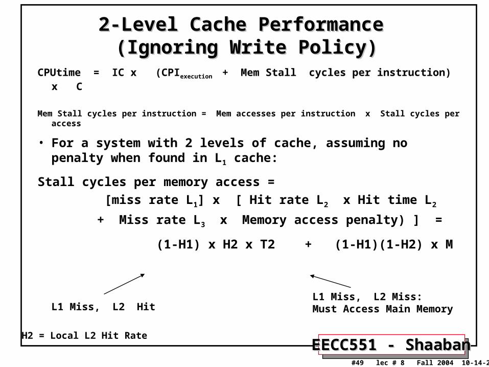
CPUtime = IC x (CPIexecution + Mem Stall cycles per instruction) x C
Mem Stall cycles per instruction = Mem accesses per instruction x Stall cycles per access
• For a system with 2 levels of cache, assuming no penalty when found in L1 cache:
Stall cycles per memory access =
[miss rate L1] x [ Hit rate L2 x Hit time L2
+ Miss rate L3 x Memory access penalty) ] =
(1-H1) x H2 x T2 + (1-H1)(1-H2) x M
2-Level Cache Performance 2-Level Cache Performance (Ignoring Write Policy)(Ignoring Write Policy)
L1 Miss, L2 HitL1 Miss, L2 Miss: Must Access Main Memory
H2 = Local L2 Hit Rate
EECC551 - ShaabanEECC551 - Shaaban#50 lec # 8 Fall 2004 10-14-2004
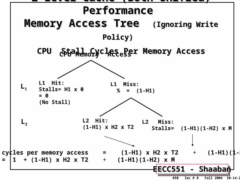
2-Level Cache (Both Unified) Performance 2-Level Cache (Both Unified) Performance Memory Access Tree Memory Access Tree (Ignoring Write Policy)(Ignoring Write Policy)
CPU Stall Cycles Per Memory AccessCPU Stall Cycles Per Memory Access
CPU Memory Access
L1 Miss: % = (1-H1)
L1 Hit:Stalls= H1 x 0 = 0(No Stall)
L2 Miss: Stalls= (1-H1)(1-H2) x M
L2 Hit:(1-H1) x H2 x T2
Stall cycles per memory access = (1-H1) x H2 x T2 + (1-H1)(1-H2) x MAMAT = 1 + (1-H1) x H2 x T2 + (1-H1)(1-H2) x M
L1
L2

EECC551 - ShaabanEECC551 - Shaaban#51 lec # 8 Fall 2004 10-14-2004
Two-Level Cache ExampleTwo-Level Cache Example• CPU with CPIexecution = 1.1 running at clock rate = 500 MHz
• 1.3 memory accesses per instruction.• L1 cache operates at 500 MHz with a miss rate of 5%
• L2 cache operates at 250 MHz with local miss rate 40%, (T2 = 2 cycles)
• Memory access penalty, M = 100 cycles. Find CPI.
CPI = CPIexecution + Mem Stall cycles per instruction
With No Cache, CPI = 1.1 + 1.3 x 100 = 131.1
With single L1, CPI = 1.1 + 1.3 x .05 x 100 = 7.6Mem Stall cycles per instruction = Mem accesses per instruction x Stall cycles per access
Stall cycles per memory access = (1-H1) x H2 x T2 + (1-H1)(1-H2) x M
= .05 x .6 x 2 + .05 x .4 x 100
= .06 + 2 = 2.06Mem Stall cycles per instruction = Mem accesses per instruction x Stall cycles per access
= 2.06 x 1.3 = 2.678
CPI = 1.1 + 2.678 = 3.778
Speedup = 7.6/3.778 = 2

EECC551 - ShaabanEECC551 - Shaaban#52 lec # 8 Fall 2004 10-14-2004
Write Policy For 2-Level Cache• Write Policy For Level 1 Cache:
– Usually Write through to Level 2 – Write allocate is used to reduce level 1 miss reads.– Use write buffer to reduce write stalls
• Write Policy For Level 2 Cache:
– Usually write back with write allocate is used. • To minimize memory bandwidth usage.
• The above 2-level cache write policy results in inclusive L2 cache since the content of L1 is also in L2
• Common in the majority of all CPUs with 2-levels of cache• As opposed to exclusive L1, L2 (e.g AMD Athlon)

EECC551 - ShaabanEECC551 - Shaaban#53 lec # 8 Fall 2004 10-14-2004
2-Level (Both Unified) Memory Access Tree2-Level (Both Unified) Memory Access Tree
L1: Write Through to L2, Write Allocate, With Perfect Write BufferL1: Write Through to L2, Write Allocate, With Perfect Write BufferL2: Write Back with Write AllocateL2: Write Back with Write Allocate
CPU Memory Access
L1 Miss:L1 Hit:Stalls Per access = 0
L2 Hit:Stalls = (1-H1) x H2 x T2
(1-H1)(H1)
L2 Miss
(1-H1) x (1-H2)
CleanStall cycles = M x (1 -H1) x (1-H2) x % clean
L2
L1
DirtyStall cycles = 2M x (1-H1) x (1-H2) x % dirty
Stall cycles per memory access = (1-H1) x H2 x T2 + M x (1 -H1) x (1-H2) x % clean + 2M x (1-H1) x (1-H2) x % dirty
= (1-H1) x H2 x T2 + (1 -H1) x (1-H2) x ( % clean x M + % dirty x 2M)
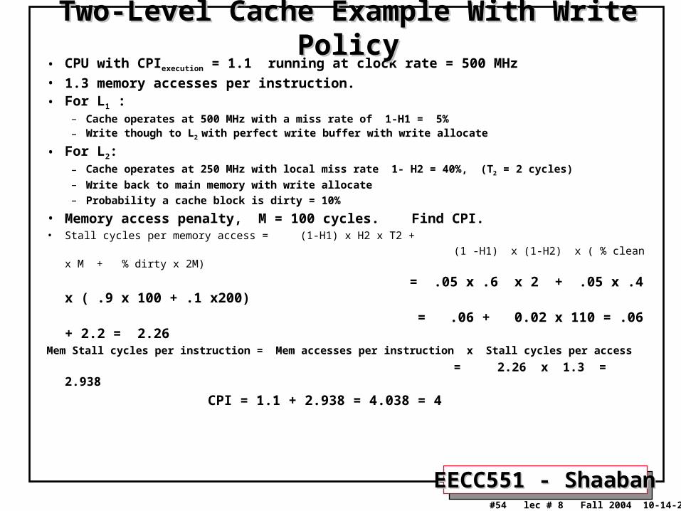
EECC551 - ShaabanEECC551 - Shaaban#54 lec # 8 Fall 2004 10-14-2004
• CPU with CPIexecution = 1.1 running at clock rate = 500 MHz
• 1.3 memory accesses per instruction.• For L1 :
– Cache operates at 500 MHz with a miss rate of 1-H1 = 5%– Write though to L2 with perfect write buffer with write allocate
• For L2:– Cache operates at 250 MHz with local miss rate 1- H2 = 40%, (T2 = 2 cycles)
– Write back to main memory with write allocate– Probability a cache block is dirty = 10%
• Memory access penalty, M = 100 cycles. Find CPI.• Stall cycles per memory access = (1-H1) x H2 x T2 +
(1 -H1) x (1-H2) x ( % clean x M + % dirty x 2M)
= .05 x .6 x 2 + .05 x .4 x ( .9 x 100 + .1 x200)
= .06 + 0.02 x 110 = .06 + 2.2 = 2.26Mem Stall cycles per instruction = Mem accesses per instruction x Stall cycles per access
= 2.26 x 1.3 = 2.938
CPI = 1.1 + 2.938 = 4.038 = 4
Two-Level Cache Example With Write PolicyTwo-Level Cache Example With Write Policy

EECC551 - ShaabanEECC551 - Shaaban#55 lec # 8 Fall 2004 10-14-2004
3 Levels of Cache3 Levels of Cache
CPU
L1 Cache
L2 Cache
L3 Cache
Main Memory
Hit Rate= H1, Hit time = 1 cycle
Hit Rate= H2, Hit time = T2 cycles
Hit Rate= H3, Hit time = T3
Memory access penalty, M

EECC551 - ShaabanEECC551 - Shaaban#56 lec # 8 Fall 2004 10-14-2004
CPUtime = IC x (CPIexecution + Mem Stall cycles per instruction) x CMem Stall cycles per instruction = Mem accesses per instruction x Stall cycles per access
• For a system with 3 levels of cache, assuming no penalty when found in L1 cache:
Stall cycles per memory access =
[miss rate L1] x [ Hit rate L2 x Hit time L2
+ Miss rate L2 x (Hit rate L3 x Hit time L3
+ Miss rate L3 x Memory access penalty) ] =
(1-H1) x H2 x T2
+ (1-H1) x (1-H2) x H3 x T3
+ (1-H1)(1-H2) (1-H3)x M
3-Level Cache Performance 3-Level Cache Performance
L1 Miss, L2 Hit
L2 Miss, L3 Hit
L1 Miss, L2 Miss: Must Access Main Memory

EECC551 - ShaabanEECC551 - Shaaban#57 lec # 8 Fall 2004 10-14-2004
3-Level Cache Performance 3-Level Cache Performance Memory Access Tree Memory Access Tree (Ignoring Write Policy)(Ignoring Write Policy)
CPU Stall Cycles Per Memory AccessCPU Stall Cycles Per Memory Access
CPU Memory Access
L1 Miss: % = (1-H1)
L1 Hit:Stalls= H1 x 0 = 0 ( No Stall)
L2 Miss: % = (1-H1)(1-H2)
L2 Hit:(1-H1) x H2 x T2
Stall cycles per memory access = (1-H1) x H2 x T2 + (1-H1) x (1-H2) x H3 x T3 + (1-H1)(1-H2) (1-H3)x MAMAT = 1 + Stall cycles per memory access
L3 Miss: (1-H1)(1-H2)(1-H3) x M
L3 Hit:(1-H1) x (1-H2) x H3 x T3
L1
L3
L2

EECC551 - ShaabanEECC551 - Shaaban#58 lec # 8 Fall 2004 10-14-2004
Three-Level Cache ExampleThree-Level Cache Example• CPU with CPIexecution = 1.1 running at clock rate = 500 MHz• 1.3 memory accesses per instruction.• L1 cache operates at 500 MHz with a miss rate of 5%• L2 cache operates at 250 MHz with a local miss rate 40%, (T2 = 2 cycles)• L3 cache operates at 100 MHz with a local miss rate 50%, (T3 = 5 cycles)• Memory access penalty, M= 100 cycles. Find CPI. With No Cache, CPI = 1.1 + 1.3 x 100 = 131.1
With single L1, CPI = 1.1 + 1.3 x .05 x 100 = 7.6
With L1, L2 CPI = 1.1 + 1.3 x (.05 x .6 x 2 + .05 x .4 x 100) = 3.778
CPI = CPIexecution + Mem Stall cycles per instruction
Mem Stall cycles per instruction = Mem accesses per instruction x Stall cycles per access
Stall cycles per memory access = (1-H1) x H2 x T2 + (1-H1) x (1-H2) x H3 x T3 + (1-H1)(1-H2) (1-H3)x M
= .05 x .6 x 2 + .05 x .4 x .5 x 5 + .05 x .4 x .5 x 100 = .097 + .0075 + .00225 = 1.11
CPI = 1.1 + 1.3 x 1.11 = 2.54 Speedup compared to L1 only = 7.6/2.54 = 3
Speedup compared to L1, L2 = 3.778/2.54 = 1.49