EEC 216 Lecture #7: Low Power Interconnectramirtha/EEC216/W08/lecture7.pdf · storage node – Many...
56
EEC 216 Lecture #7: Low Power Interconnect Rajeevan Amirtharajah University of California, Davis
Transcript of EEC 216 Lecture #7: Low Power Interconnectramirtha/EEC216/W08/lecture7.pdf · storage node – Many...

EEC 216 Lecture #7:Low Power Interconnect
Rajeevan AmirtharajahUniversity of California, Davis

R. Amirtharajah, EEC216 Winter 2008 2
Outline
• Announcements
• Review: Sizing, Clocking, Latches & Flip-Flops
• Low Swing Buses and Level Converters
• Stepwise Charging
• Data Dependent Swings
• Bus Invert Coding
• Modulated Signaling

R. Amirtharajah, EEC216 Winter 2008 3
Corrected Total Capacitance Model
• Total capacitance per unit length is parallel-plate (area) term plus fringing-field term:
• Model is simple and works fairly well
– More sophisticated numerical models also available
• Process models often give both area and fringing (also known as sidewall) capacitance numbers per unit length of wire for each interconnect layer
( )12log2
++=+=
HttWccc rr
fringeppπεε

R. Amirtharajah, EEC216 Winter 2008 4
Announcements

R. Amirtharajah, EEC216 Winter 2008 5
Outline
• Announcements
• Review: Sizing, Clocking, Latches & Flip-Flops
• Low Swing Buses and Level Converters
• Stepwise Charging
• Data Dependent Swings
• Bus Invert Coding
• Modulated Signaling
R. Amirtharajah, EEC216 Winter 2008 6
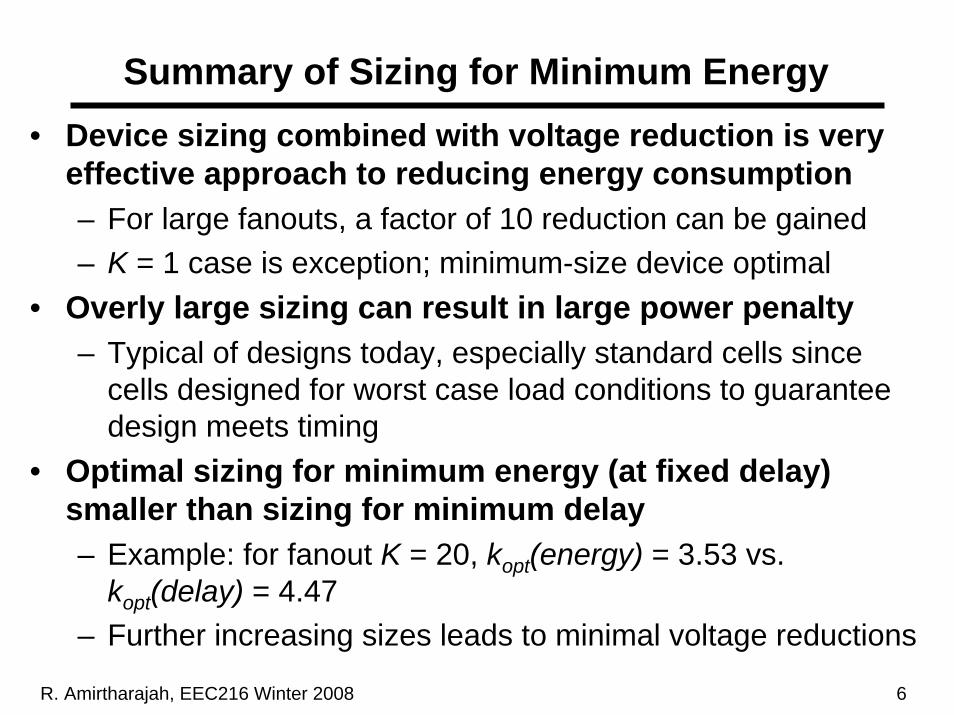
Summary of Sizing for Minimum Energy• Device sizing combined with voltage reduction is very
effective approach to reducing energy consumption– For large fanouts, a factor of 10 reduction can be gained– K = 1 case is exception; minimum-size device optimal
• Overly large sizing can result in large power penalty– Typical of designs today, especially standard cells since
cells designed for worst case load conditions to guarantee design meets timing
• Optimal sizing for minimum energy (at fixed delay) smaller than sizing for minimum delay– Example: for fanout K = 20, kopt(energy) = 3.53 vs.
kopt(delay) = 4.47– Further increasing sizes leads to minimal voltage reductions

R. Amirtharajah, EEC216 Winter 2008 7
Synchronous System With Global Clock
• Simple and convenient design style with minimal circuit overhead
• Challenge is creating and distributing clock with low skew and jitter (timing uncertainty) at high frequencies
LOGIC LOGIC
CLK
Reference from PLL
R. Amirtharajah, EEC216 Winter 2008 8
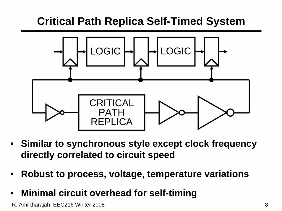
Critical Path Replica Self-Timed System
LOGIC LOGIC
CRITICALPATH
REPLICA
• Similar to synchronous style except clock frequency directly correlated to circuit speed
• Robust to process, voltage, temperature variations
• Minimal circuit overhead for self-timing
R. Amirtharajah, EEC216 Winter 2008 9
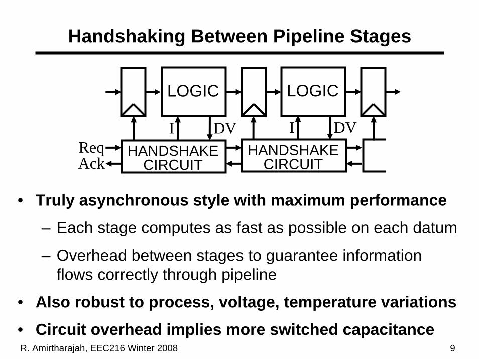
Handshaking Between Pipeline Stages
LOGIC LOGIC
HANDSHAKECIRCUIT
I DVHANDSHAKE
CIRCUIT
I DVReqAck
• Truly asynchronous style with maximum performance– Each stage computes as fast as possible on each datum
– Overhead between stages to guarantee information flows correctly through pipeline
• Also robust to process, voltage, temperature variations • Circuit overhead implies more switched capacitance
R. Amirtharajah, EEC216 Winter 2008 10
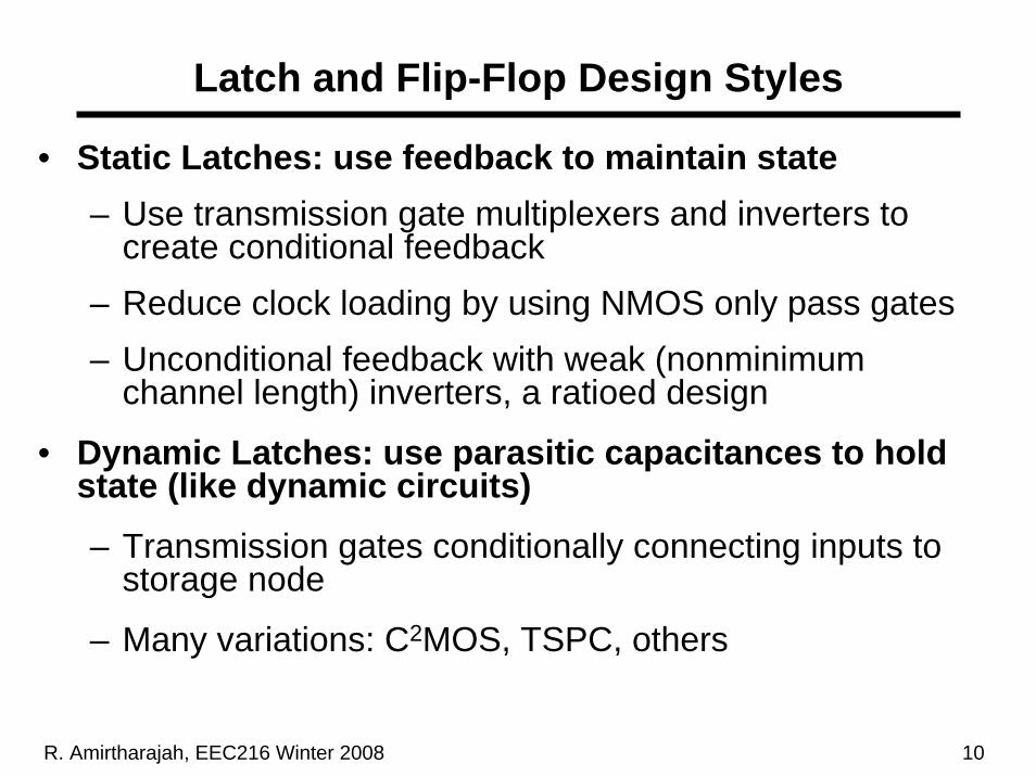
Latch and Flip-Flop Design Styles
• Static Latches: use feedback to maintain state– Use transmission gate multiplexers and inverters to
create conditional feedback– Reduce clock loading by using NMOS only pass gates– Unconditional feedback with weak (nonminimum
channel length) inverters, a ratioed design
• Dynamic Latches: use parasitic capacitances to hold state (like dynamic circuits)
– Transmission gates conditionally connecting inputs to storage node
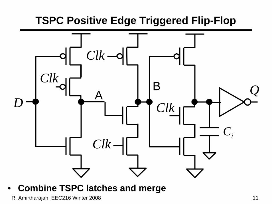
– Many variations: C2MOS, TSPC, others
R. Amirtharajah, EEC216 Winter 2008 11
TSPC Positive Edge Triggered Flip-Flop
• Combine TSPC latches and merge
ClkiC
QClkD
Clk
Clk
AB

R. Amirtharajah, EEC216 Winter 2008 12
Outline
• Announcements
• Review: Sizing, Clocking, Latches & Flip-Flops
• Low Swing Buses and Level Converters
• Stepwise Charging
• Data Dependent Swings
• Bus Invert Coding
• Modulated Signaling
R. Amirtharajah, EEC216 Winter 2008 13
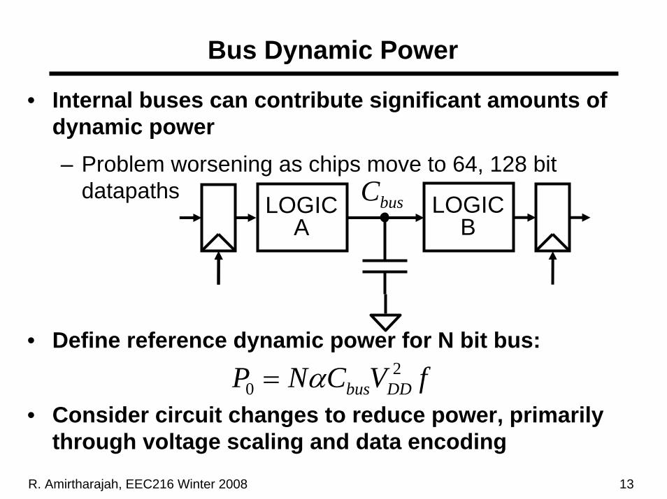
• Internal buses can contribute significant amounts of dynamic power– Problem worsening as chips move to 64, 128 bit
datapaths
• Define reference dynamic power for N bit bus:
• Consider circuit changes to reduce power, primarily through voltage scaling and data encoding
fVCNP DDbus2
0 α=
Bus Dynamic Power
LOGICA
LOGICB
busC

R. Amirtharajah, EEC216 Winter 2008 14
Reduced Voltage Swing
LOGICA
LOGICB
busCn1
× n×
• Driver circuit attenuates voltage swing toward ground for large on-chip buses
• Receiver amplifies small swings to rail-to-rail• Quadratic reduction in bus power
RcvrDriver
R. Amirtharajah, EEC216 Winter 2008 15
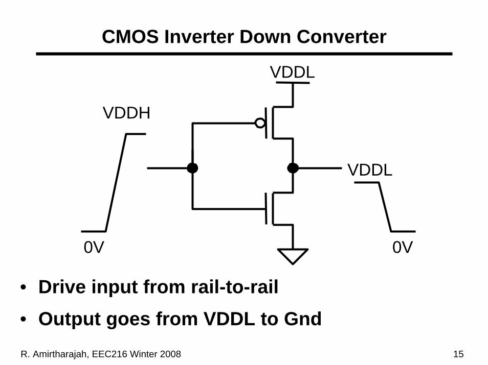
CMOS Inverter Down Converter
VDDL
VDDH
0V
VDDL
0V
• Drive input from rail-to-rail• Output goes from VDDL to Gnd
R. Amirtharajah, EEC216 Winter 2008 16
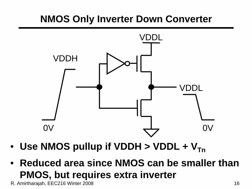
NMOS Only Inverter Down Converter
VDDL
VDDH
0V
VDDL
0V
• Use NMOS pullup if VDDH > VDDL + VTn
• Reduced area since NMOS can be smaller than PMOS, but requires extra inverter
R. Amirtharajah, EEC216 Winter 2008 17
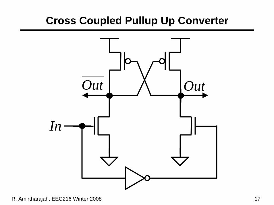
Cross Coupled Pullup Up Converter
Out
In
Out
R. Amirtharajah, EEC216 Winter 2008 18
Cross Coupled Up Converter Design
• Similar issues to sense amp flip-flop design– Design input NMOS pair to flip state of converter– Potentially fast since input swings can be small, less
time required to develop adequate differential voltage on large capacitance bus lines
• Several analog design issues– Ratioed differential design like DCVSL– Sensitive to P/N mismatch corner– Threshold voltage variation results in variable speed
• Can fold in logic to form DCVSL gate• Also fold in edge-triggered flip-flop for retiming
R. Amirtharajah, EEC216 Winter 2008 19
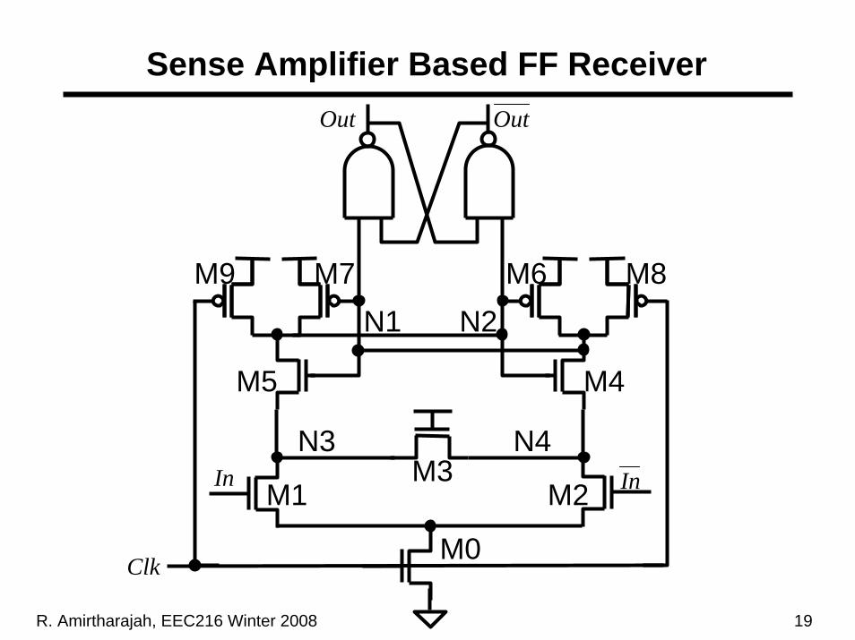
Sense Amplifier Based FF Receiver
M0Clk
In In
Out Out
M3M1 M2
M5 M4
M9 M7 M6 M8
N3 N4
N1 N2

R. Amirtharajah, EEC216 Winter 2008 20
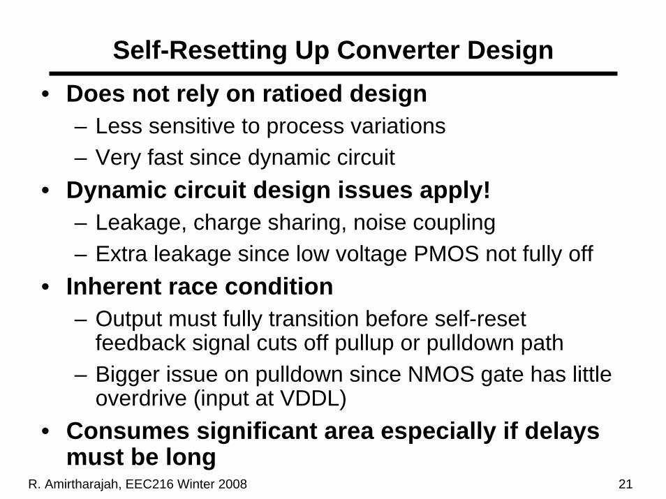
Self-Resetting Up Converter
Out
In
Inverting Delay
R. Amirtharajah, EEC216 Winter 2008 21
Self-Resetting Up Converter Design• Does not rely on ratioed design
– Less sensitive to process variations– Very fast since dynamic circuit
• Dynamic circuit design issues apply!– Leakage, charge sharing, noise coupling– Extra leakage since low voltage PMOS not fully off
• Inherent race condition– Output must fully transition before self-reset
feedback signal cuts off pullup or pulldown path– Bigger issue on pulldown since NMOS gate has little
overdrive (input at VDDL)• Consumes significant area especially if delays
must be long
R. Amirtharajah, EEC216 Winter 2008 22
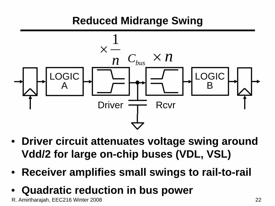
Reduced Midrange Swing
LOGICA
LOGICB
busCn1
× n×
• Driver circuit attenuates voltage swing around Vdd/2 for large on-chip buses (VDL, VSL)
• Receiver amplifies small swings to rail-to-rail• Quadratic reduction in bus power
RcvrDriver
R. Amirtharajah, EEC216 Winter 2008 23
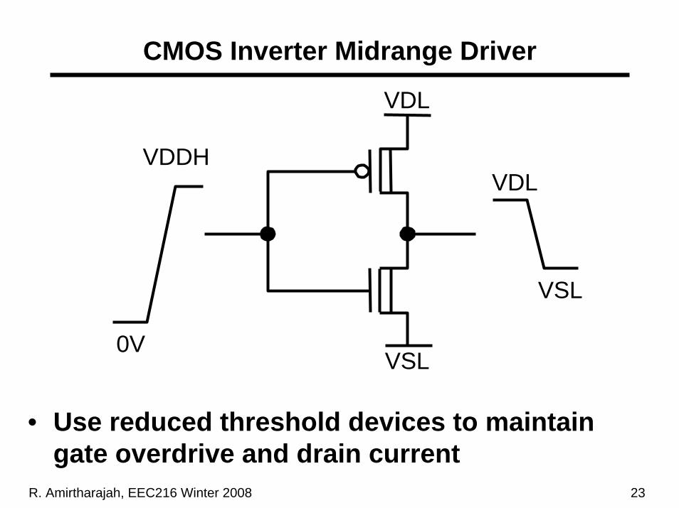
CMOS Inverter Midrange Driver
VDL
VDDH
0V
VDL
VSL
• Use reduced threshold devices to maintain gate overdrive and drain current
VSL

R. Amirtharajah, EEC216 Winter 2008 24
Symmetric Level Converter
InOut
VSL
VDL
1
2

R. Amirtharajah, EEC216 Winter 2008 25
• Both pass gates pull internal nodes to VDL, causing positive feedback to switch output rail-to-rail
In
Out
1
Symmetric Level Converter Operation
2VDL
VSL
VDDH
0V
R. Amirtharajah, EEC216 Winter 2008 26
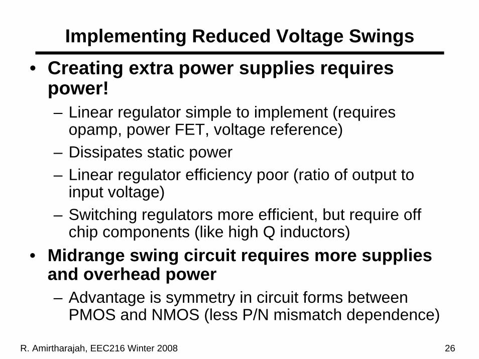
Implementing Reduced Voltage Swings• Creating extra power supplies requires
power!– Linear regulator simple to implement (requires
opamp, power FET, voltage reference)– Dissipates static power– Linear regulator efficiency poor (ratio of output to
input voltage)– Switching regulators more efficient, but require off
chip components (like high Q inductors)• Midrange swing circuit requires more supplies
and overhead power– Advantage is symmetry in circuit forms between
PMOS and NMOS (less P/N mismatch dependence)
R. Amirtharajah, EEC216 Winter 2008 27
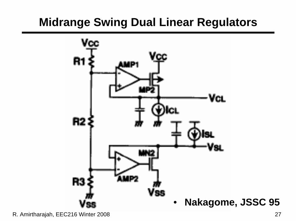
Midrange Swing Dual Linear Regulators
• Nakagome, JSSC 95
R. Amirtharajah, EEC216 Winter 2008 28
Outline
• Announcements
• Review: Sizing, Clocking, Latches & Flip-Flops
• Low Swing Buses and Level Converters
• Stepwise Charging
• Data Dependent Swings
• Bus Invert Coding
• Modulated Signaling
R. Amirtharajah, EEC216 Winter 2008 29
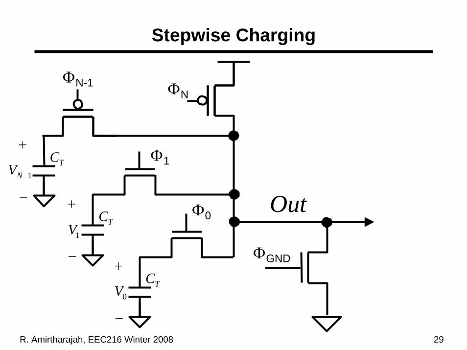
Stepwise Charging
TC+
−
1−NV
TC+
−
1V
TC+
−
0V
ΦNΦN-1
Φ1
Φ0
ΦGND
Out
R. Amirtharajah, EEC216 Winter 2008 30
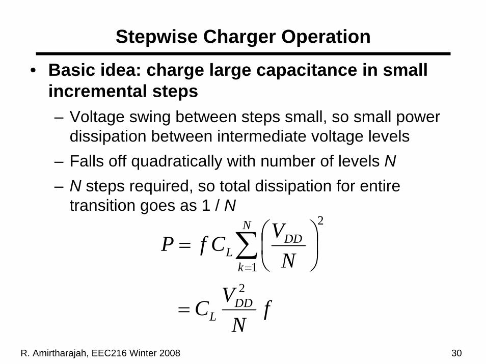
Stepwise Charger Operation
• Basic idea: charge large capacitance in small incremental steps– Voltage swing between steps small, so small power
dissipation between intermediate voltage levels– Falls off quadratically with number of levels N– N steps required, so total dissipation for entire
transition goes as 1 / N
fN
VC DDL
2
=
2
1∑
=⎟⎠⎞
⎜⎝⎛=
N
k
DDL N
VCfP
R. Amirtharajah, EEC216 Winter 2008 31
Stepwise Charger Design• Requires large tank capacitors to store
intermediate voltage levels– Must store enough charge that charge sharing with
output node doesn’t affect voltage much, share among multiple drivers
– Unnecessary to generate intermediate voltages independently
– Charge redistribution after several cycles of operation charges tank capacitors to intermediate levels
• Implement switches with two FETs in parallel– One sized for charging transition, other for
discharging transition– Reduces losses due to driving switch gates

R. Amirtharajah, EEC216 Winter 2008 32
Stepwise Charger Optimization
• Controller generates timing signals to control charging and discharging– More steps (N bigger), less power in driving load– However, more power due to driving switch gates– Tradeoff results in optimum number of steps for
lowest power dissipation:
– T: desired rise time of driver output– RC: intrinsic switching speed of process– m: number of RC time constants for each charging
step
34mRC
TNopt =

R. Amirtharajah, EEC216 Winter 2008 33
Stepwise Charger Summary• Is it practical?
– Requires large (presumably off-chip) capacitors– Shallow minimum, so less constrained– Often requires only 3-4 voltage steps to get within a
few percent of minimum power• Some care required for generating timing
signals– Avoid overlap: can result in voltage steps being
averaged together– Use edge-to-pulse converters with controlled delay
elements to meet worst case pulse width requirements
• First example of adiabatic circuit techniques
R. Amirtharajah, EEC216 Winter 2008 34
Outline
• Announcements
• Review: Sizing, Clocking, Latches & Flip-Flops
• Low Swing Buses and Level Converters
• Stepwise Charging
• Data Dependent Swings
• Bus Invert Coding
• Modulated Signaling
R. Amirtharajah, EEC216 Winter 2008 35
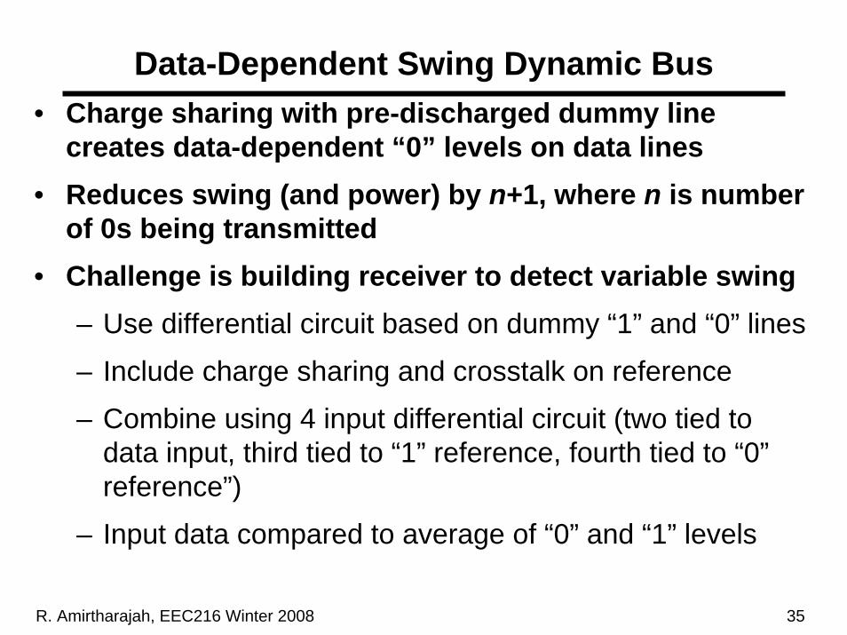
Data-Dependent Swing Dynamic Bus• Charge sharing with pre-discharged dummy line
creates data-dependent “0” levels on data lines• Reduces swing (and power) by n+1, where n is number
of 0s being transmitted• Challenge is building receiver to detect variable swing
– Use differential circuit based on dummy “1” and “0” lines
– Include charge sharing and crosstalk on reference
– Combine using 4 input differential circuit (two tied to data input, third tied to “1” reference, fourth tied to “0”reference”)
– Input data compared to average of “0” and “1” levels
R. Amirtharajah, EEC216 Winter 2008 36
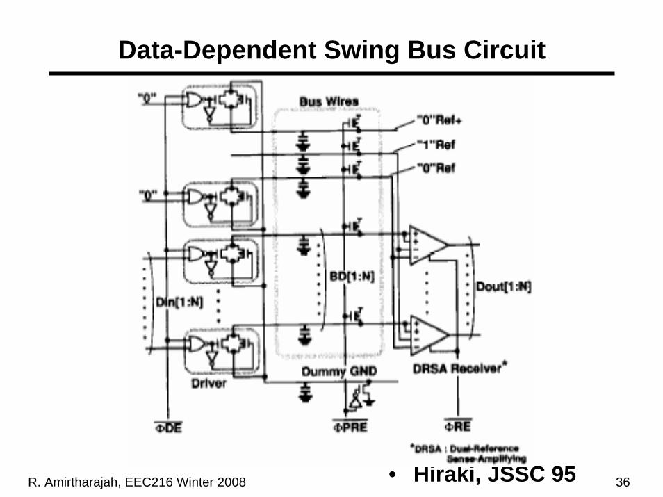
Data-Dependent Swing Bus Circuit
• Hiraki, JSSC 95
R. Amirtharajah, EEC216 Winter 2008 37
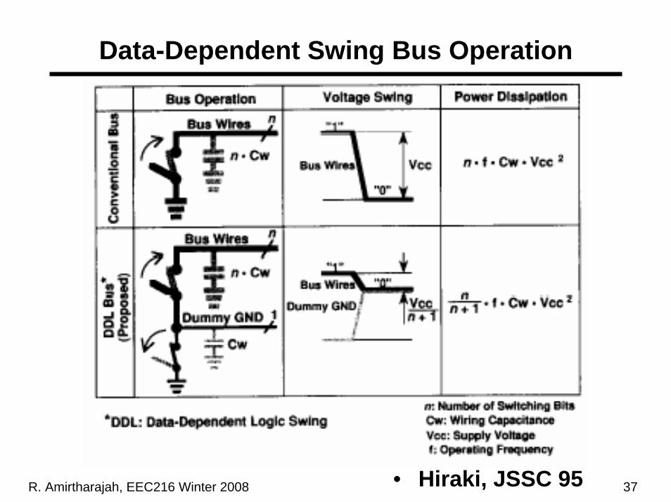
Data-Dependent Swing Bus Operation
• Hiraki, JSSC 95
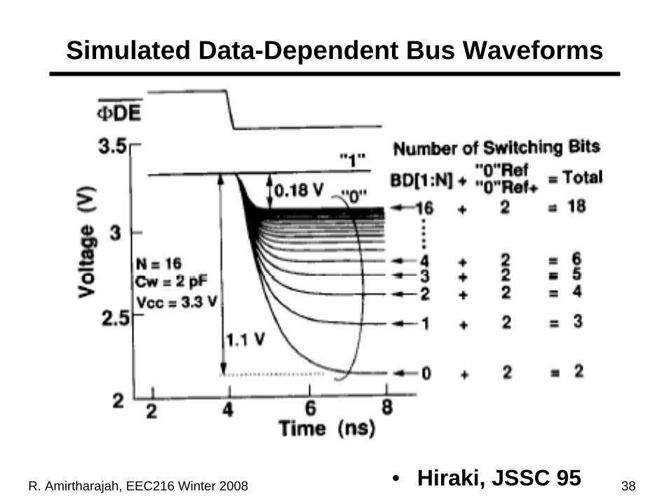
R. Amirtharajah, EEC216 Winter 2008 38
Simulated Data-Dependent Bus Waveforms
• Hiraki, JSSC 95
R. Amirtharajah, EEC216 Winter 2008 39
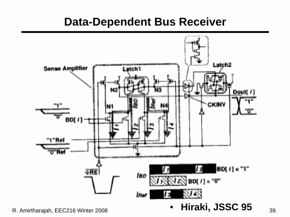
Data-Dependent Bus Receiver
• Hiraki, JSSC 95
R. Amirtharajah, EEC216 Winter 2008 40
Data-Dependent Bus Issues• Dynamic bus so dynamic circuit design rules apply!• Some overhead in dummy lines
– Four extra wires if follow design from Hiraki paper
– Must amortize over wide bus, but wider bus implies smaller voltage swing in worst case
• Complicated receiver consumes area, short circuit current while switching– Differential circuit design rules apply
– Power cost implies optimal ratio between number of data lines and dummy lines, i.e. optimal bus width
• If receiver can be built, why not just use reduced swing at minimum receiver threshold?

R. Amirtharajah, EEC216 Winter 2008 41
Outline
• Announcements
• Review: Sizing, Clocking, Latches & Flip-Flops
• Low Swing Buses and Level Converters
• Stepwise Charging
• Data Dependent Swings
• Bus Invert Coding
• Modulated Signaling
R. Amirtharajah, EEC216 Winter 2008 42
Coding for Low Power Interconnect
• Goal is to reduce number of transitions on bus– Techniques explored in past to reduce Ldi/dt
(simultaneous switching noise) on output pads – Bus-Invert coding special case of “starvation coding”
or “limited-weight coding”• Tradeoff between reduced activity and circuit
overhead– Extra wires needed on bus– Encoding circuitry can be complicated, consumes
more power• Still an area of active research!
R. Amirtharajah, EEC216 Winter 2008 43
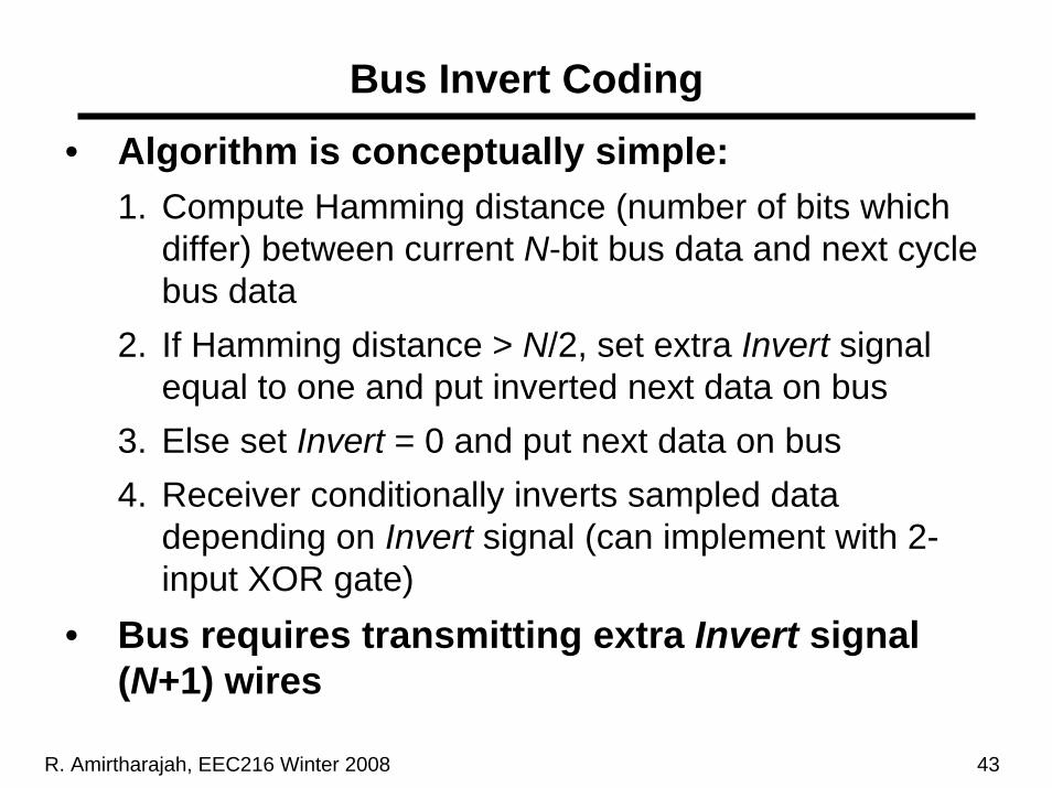
Bus Invert Coding
• Algorithm is conceptually simple:1. Compute Hamming distance (number of bits which
differ) between current N-bit bus data and next cycle bus data
2. If Hamming distance > N/2, set extra Invert signal equal to one and put inverted next data on bus
3. Else set Invert = 0 and put next data on bus4. Receiver conditionally inverts sampled data
depending on Invert signal (can implement with 2-input XOR gate)
• Bus requires transmitting extra Invert signal (N+1) wires

R. Amirtharajah, EEC216 Winter 2008 44
Bus Invert Coding Performance• Maximum number of transitions reduced from N
to N/2, assuming uniform and independent bits – Peak dynamic power cut in half– Average number of transitions reduced by less than
half due to additional Invert signal and binomial distribution in Hamming distance
– With invert coding, N/2 becomes most likely Hamming distance so inverting data values makes no difference
• As N gets bigger, average power savings becomes smaller– N=8, 18% less average power, but only 15% savings
at N=16• Scheme optimal for overhead of one extra wire

R. Amirtharajah, EEC216 Winter 2008 45
Partitioned Code for Lower Average Power
• Divide N bit bus into smaller buses and encode those separately– Reduces average power dissipation most (limit is
N=2, with N/2 additional invert signals)– N=2 limit results in 25% lower activity
• Other codes using more than one extra wire can reduce activity even further– Code generation challenging, could use lookup
tables but would cost a lot of area, power– M-limited weight codes are one approach (M is
maximum number of transitions between cycles)– Number of extra wires grows exponentially
R. Amirtharajah, EEC216 Winter 2008 46
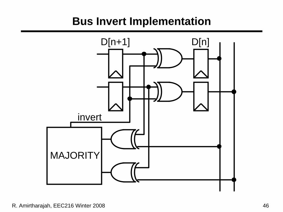
Bus Invert Implementation
D[n]
MAJORITY
D[n+1]
invert
R. Amirtharajah, EEC216 Winter 2008 47
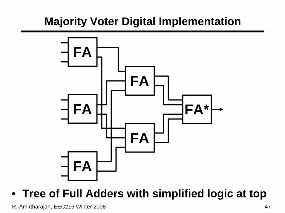
Majority Voter Digital Implementation
FA
FA
FA
FA
FA
FA*
• Tree of Full Adders with simplified logic at top
R. Amirtharajah, EEC216 Winter 2008 48
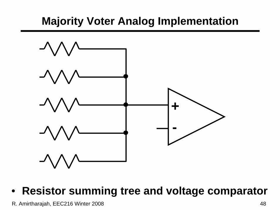
Majority Voter Analog Implementation
• Resistor summing tree and voltage comparator
+-
R. Amirtharajah, EEC216 Winter 2008 49
Gray Code for Low Power
• For sequential data streams Gray coding reduces activity– Only one wire out of N transitions in any given cycle– Extra circuit and extra area required
• Useful for address traces which tend to be sequential– Program counter, FIFO pointers, indices for arrays
stored in RAM– Sequential FSM states
• Mix of Gray code and Bus-Invert coding deals with combined random and sequential traces
R. Amirtharajah, EEC216 Winter 2008 50
Impact of Data Statistics on Coding
• Bus invert coding assumes random signals– Empirically signal processing data streams exhibit
Dual Bit-Type behavior– Use bus invert coding on random LSBs– MSBs don’t transition much anyway

R. Amirtharajah, EEC216 Winter 2008 51
Outline
• Announcements
• Review: Sizing, Clocking, Latches & Flip-Flops
• Low Swing Buses and Level Converters
• Stepwise Charging
• Data Dependent Swings
• Bus Invert Coding
• Modulated Signaling

R. Amirtharajah, EEC216 Winter 2008 52
Binary NRZ vs. Modulated RZ
Baseband NRZ: Bit Rate = 1/T
T
Pulse width = T
T
PM/PWM RZ: Bit Rate = (1+m1+m2)/(2T+n1δ1+n2δ2)
T
Symbol width = 2T+n1δ1+n2δ2
T
δ2 δ2δ1 δ1
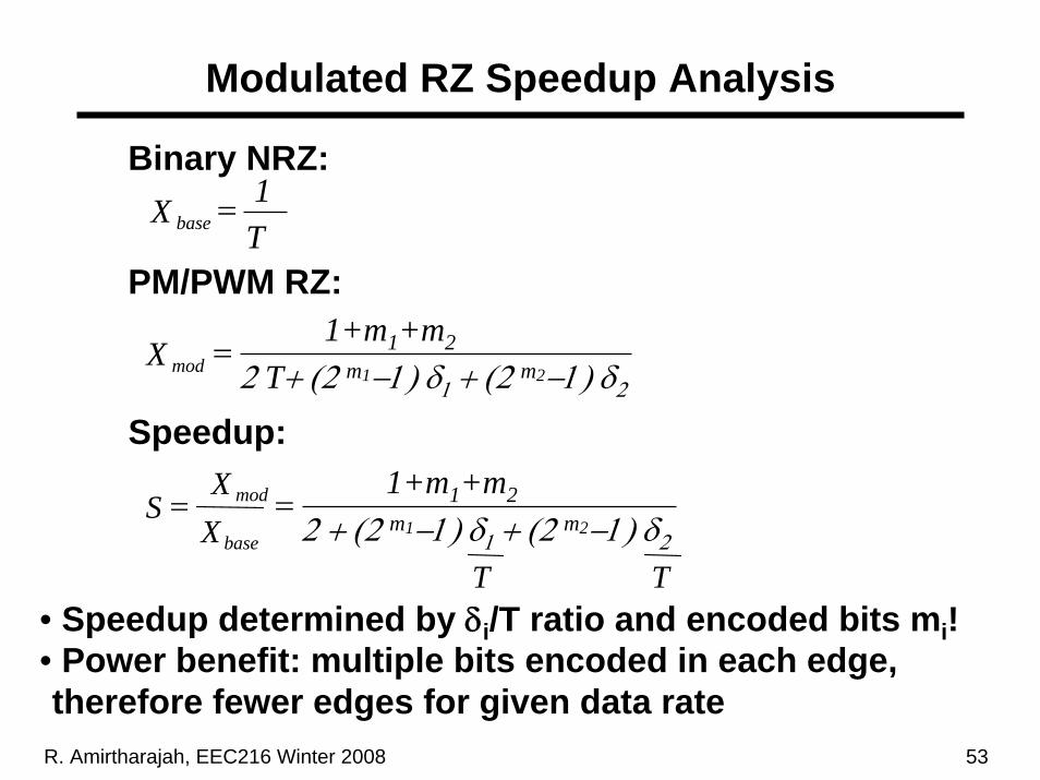
R. Amirtharajah, EEC216 Winter 2008 53
Modulated RZ Speedup Analysis
modX1+m1+m2
2 T+ (2 m1−1) δ1 + (2 m2−1) δ2=
base
mod
XX
S =
Binary NRZ:
PM/PWM RZ:
baseXT1=
Speedup:1+m1+m2
2 + (2 m1−1) δ1 + (2 m2−1) δ2=
T T• Speedup determined by δi/T ratio and encoded bits mi!• Power benefit: multiple bits encoded in each edge, therefore fewer edges for given data rate
R. Amirtharajah, EEC216 Winter 2008 54
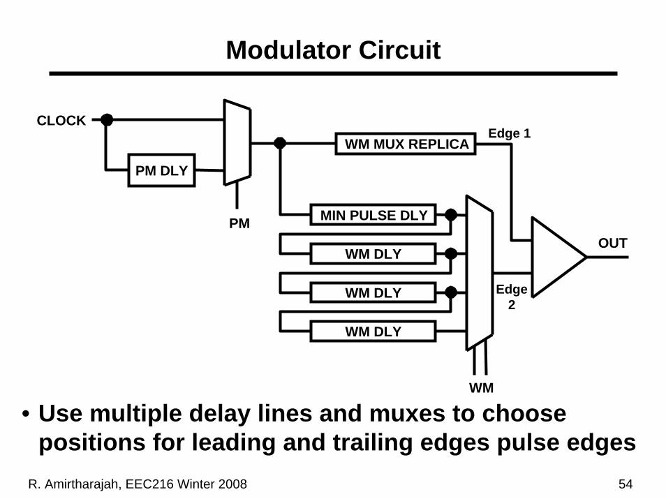
Edge 2
WM MUX REPLICA
MIN PULSE DLY
WM DLY
WM DLY
WM DLY
WM
Edge 1
PM
PM DLY
CLOCK
OUT
• Use multiple delay lines and muxes to choose positions for leading and trailing edges pulse edges
Modulator Circuit
R. Amirtharajah, EEC216 Winter 2008 55
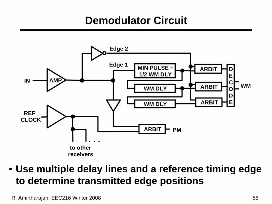
Edge 2
MIN PULSE +1/2 WM DLY
WM DLY
WM DLY
Edge 1
ARBIT
ARBIT
DECODE
WMAMP
REFCLOCK
. . .to other
receivers
ARBIT
ARBIT PM
IN
• Use multiple delay lines and a reference timing edge to determine transmitted edge positions
Demodulator Circuit
R. Amirtharajah, EEC216 Winter 2008 56
Conclusions
• Interconnect power an increasingly important component of total chip power– Wires aren’t scaling as fast as transistors (to
maintain reasonable resistance)– Chips tend to get larger, use faster data rates
• Numerous good (and bad) techniques proposed– Many rely on low voltage swings on long wires,
require amplifiers, possibly more static power– Data coded to reduce transitions (requires logic
overhead)– Modulated signaling to transmit several bits per edge
• Ongoing area of research!


![Program Review and Standards Handbook...Information about RAC meetings can be found by going to the TSPC website, select [Rules & Statutes] on the left-hand navigation panel, then](https://static.fdocuments.us/doc/165x107/5f453cef3ca275678f769bcf/program-review-and-standards-handbook-information-about-rac-meetings-can-be.jpg)