EE143 F2010 Lecture 22 Electrical Characteristics of MOS ...ee143/fa10/lectures/Lec_22.pdf ·...
36
Professor N Cheung, U.C. Berkeley Lecture 22 EE143 F2010 1 Electrical Characteristics of MOS Devices • The MOS Capacitor – Voltage components – Accumulation, Depletion, Inversion Modes – Effect of channel bias and substrate bias – Effect of gate oxide charges – Threshold-voltage adjustment by implantation – Capacitance vs. voltage characteristics • MOS Field-Effect Transistor – I-V characteristics – Parameter extraction “metal” oxide semiconductor V G + x ox “metal” oxide semiconductor V G + x ox
Transcript of EE143 F2010 Lecture 22 Electrical Characteristics of MOS ...ee143/fa10/lectures/Lec_22.pdf ·...

Professor N Cheung, U.C. Berkeley
Lecture 22EE143 F2010
1
Electrical Characteristics of MOS Devices
• The MOS Capacitor
– Voltage components
– Accumulation, Depletion, Inversion Modes
– Effect of channel bias and substrate bias
– Effect of gate oxide charges
– Threshold-voltage adjustment by implantation
– Capacitance vs. voltage characteristics
• MOS Field-Effect Transistor
– I-V characteristics
– Parameter extraction
“metal”
oxide
semiconductor
VG
+
xox
“metal”
oxide
semiconductor
VG
+
xox

Professor N Cheung, U.C. Berkeley
Lecture 22EE143 F2010
2
2) Visit the Device Visualization Website
http://jas.eng.buffalo.edu/
and run the visualization experiments of
1) Charge carriers and Fermi level,
2) pn junctions
3) MOS capacitors
4) MOSFETs
1) Reading Assignment
Streetman: Section of Streetman Chap 8 on MOS

Professor N Cheung, U.C. Berkeley
Lecture 22EE143 F2010
3
Work Function of Materials
Eo
EV
ECq
SEMICONDUCTOR
Ef
Eo
Ef
METAL
Work function
= q
Vacuum
energy level
qM is determined
by the metal material
qS is determined
by the semiconductor material,
the dopant type,
and doping concentration

Professor N Cheung, U.C. Berkeley
Lecture 22EE143 F2010
4
Work Function (qM) of MOS Gate Materials
Eo = vacuum energy level Ef = Fermi level
EC = bottom of conduction band EV = top of conduction
band
Ef
Examples:
Al = 4.1 eV
TiSi2 = 4.6 eV
Ef
Eo
qM
Eo
qM
Ei
EC
EV
0.56eV
q = 4.15eV
0.56eV
q = 4.15eV (electron affinity)
Eo
Ei
EC
EV
0.56eV
q = 4.15eV
0.56eV
Ef
n+ poly-Si
(Ef = EC)p+ poly-Si
(Ef = EV)
qM

Professor N Cheung, U.C. Berkeley
Lecture 22EE143 F2010
5
Work Function of doped Si substrate
q = 4.15eV
Ef
Eo
qs
Ei
EC
EV
|qF|
0.56eV
0.56eV
* Depends on substrate concentration NB
Ef
Eo
qs
Ei
EC
EV
|qF|
0.56eV
0.56eV
q = 4.15eV
n-type Si p-type Si
s (volts) = 4.15 +0.56 - |F| s (volts) = 4.15 +0.56 + |F|
i
BF
n
N
q
kTln

Professor N Cheung, U.C. Berkeley
Lecture 22EE143 F2010
6
The MOS Capacitor
SioxFBG VVVV
ox
oxox
xC
[in Farads /cm2]
+_ VFB
Vox (depends on VG)
Vsi (depends on VG)
+
_
+
_
“metal”
oxide
semiconductor
VG
+
xox
Oxide capacitance/unit area
Professor N Cheung, U.C. Berkeley
Lecture 22EE143 F2010
7
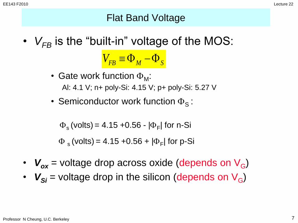
Flat Band Voltage
• VFB is the “built-in” voltage of the MOS:
• Gate work function M:
Al: 4.1 V; n+ poly-Si: 4.15 V; p+ poly-Si: 5.27 V
• Semiconductor work function S :
• Vox = voltage drop across oxide (depends on VG)
• VSi = voltage drop in the silicon (depends on VG)
SMFBV
s (volts) = 4.15 +0.56 - |F| for n-Si
s (volts) = 4.15 +0.56 + |F| for p-Si

Professor N Cheung, U.C. Berkeley
Lecture 22EE143 F2010
8
A) Accumulation: VG < VFB for p-type substrate
VSi 0, so Vox = VG - VFB
QSi’ = charge/unit area in Si
=Cox (VG - VFB )
MOS Operation Modes
M O Si (p-Si)
Thickness of accumulation layer ~0
holes
Charge Distribution

Professor N Cheung, U.C. Berkeley
Lecture 22EE143 F2010
9
MOS Operation Modes
• B) Flatband Condition : VG = VFB
No charge in Si (and hence no charge in metal gate)
• VSi = Vox = 0
M O S (p-Si)
Charge Distribution

Professor N Cheung, U.C. Berkeley
Lecture 22EE143 F2010
10
C) Depletion: VG > VFB
MOS Operation Modes (cont.)
M O S (p-Si)
qNB
xd
s
2
dB
ox
dBFBG
2
xqN
C
xqNVV
(For given VG, can solve for xd)
B
SiSid
qN
V2x
VoxVSi
Depletion layer
Charge Distribution
Depletion
Layer
thickness
Note: NBxd is the total
charge in Si /unit area

Professor N Cheung, U.C. Berkeley
Lecture 22EE143 F2010
11
x
x=0
Q'
Metal
(x)
Oxide
x=xo
x
xd
x=0
Q'
Metal Semiconductor
(x)
Oxide
x=xo
x=xo+
Q'-
x
xd
x=0
Q'
Metal Semiconductor
(x)
Oxide
x=xo
x=xo+
Semiconductor
Depletion Mode :Charge and Electric Field Distributions
by Superposition Principle of Electrostatics
x
xd
x=0
Metal SemiconductorE(x)
Oxide
x=xo
x=xo+
x
xd
x=0
Metal Semiconductor
E(x)
Oxide
x=xo
x=xo+
x
xd
x=0
Metal Semiconductor
E(x)
Oxide
x=xo
x=xo+
=+
Professor N Cheung, U.C. Berkeley
Lecture 22EE143 F2010
12
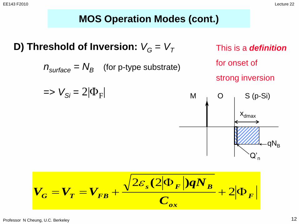
D) Threshold of Inversion: VG = VT
nsurface = NB (for p-type substrate)
=> VSi = 2|F|
MOS Operation Modes (cont.)
M O S (p-Si)
qNB
xdmax
F
ox
BFs
FBTGC
qNVVV
2
22 )(
Q’n
This is a definition
for onset of
strong inversion

Professor N Cheung, U.C. Berkeley
Lecture 22EE143 F2010
13
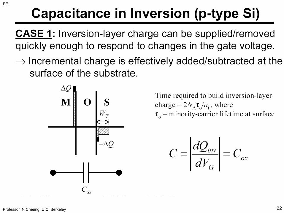
E) Strong Inversion: VG > VT
MOS Operation Modes (cont.)
M O S (p-Si)
qNa
xdmax
)(
max
TGoxn
ox
ndB
ox
VVCQ
C
QxqNV
B
FSi
dqN
x
4
max
Q’n
electrons
xdmax is approximately unchanged
when VG> VT

Professor N Cheung, U.C. Berkeley
Lecture 22EE143 F2010
14

Professor N Cheung, U.C. Berkeley
Lecture 22EE143 F2010
15

Professor N Cheung, U.C. Berkeley
Lecture 22EE143 F2010
16
p-Si

Professor N Cheung, U.C. Berkeley
Lecture 22EE143 F2010
17
Accumulation
Depletion
Inversion
Vox = Qa/Cox
VSi ~ 0
Vox =qNaxd/Cox
VSi = qNaxd2/(2s)
Vox = [qNaxdmax+Qn]/Cox
VSi = qNaxdmax2/(2s)
= 2|F|
Voltage drop = area under E-field curve
* For simplicity, dielectric constants assumed to be same for oxide and Si in E-field sketches

Professor N Cheung, U.C. Berkeley
Lecture 22EE143 F2010
18
Most derivations for MOS shown in lecture notes
are done with p-type substrate (NMOS)
as example.
Repeat the derivations yourself for n-type substrate
(PMOS) to test your understanding of MOS.
Suggested Exercise
Professor N Cheung, U.C. Berkeley
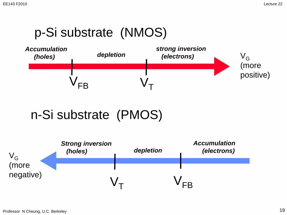
Lecture 22EE143 F2010
19
VG
(more
positive)VFB VT
Accumulation
(holes) depletionstrong inversion
(electrons)
p-Si substrate (NMOS)
n-Si substrate (PMOS)
VG
(more
negative)VFBVT
Accumulation
(electrons)depletionStrong inversion
(holes)

Professor N Cheung, U.C. Berkeley
Lecture 22EE143 F2010
20

Professor N Cheung, U.C. Berkeley
Lecture 22EE143 F2010
21
Professor N Cheung, U.C. Berkeley
Lecture 22EE143 F2010
22

Professor N Cheung, U.C. Berkeley
Lecture 22EE143 F2010
23

Professor N Cheung, U.C. Berkeley
Lecture 22EE143 F2010
24
Professor N Cheung, U.C. Berkeley
Lecture 22EE143 F2010
25
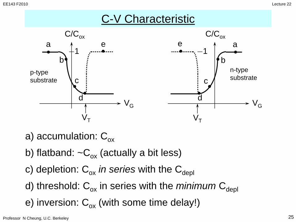
C-V Characteristic
C/Cox
VT
1
VG
p-type
substrate
a
c
d
b
e
C/Cox
VT
1
VG
n-type
substrate
a
c
d
b
e
a) accumulation: Cox
b) flatband: ~Cox (actually a bit less)
c) depletion: Cox in series with the Cdepl
d) threshold: Cox in series with the minimum Cdepl
e) inversion: Cox (with some time delay!)

Professor N Cheung, U.C. Berkeley
Lecture 22EE143 F2010
26
Accumulation
Depletion
Inversion
Q
Q
Q
Q
Q
Q
Low frequency High frequency
Q
Q
All frequencies
All frequencies
C = Cox
C = Cox 1/C = 1/Cox + xdmax/s
1/C = 1/Cox + xd/s
Small signal charge response Q due to VG
Professor N Cheung, U.C. Berkeley
Lecture 22EE143 F2010
27
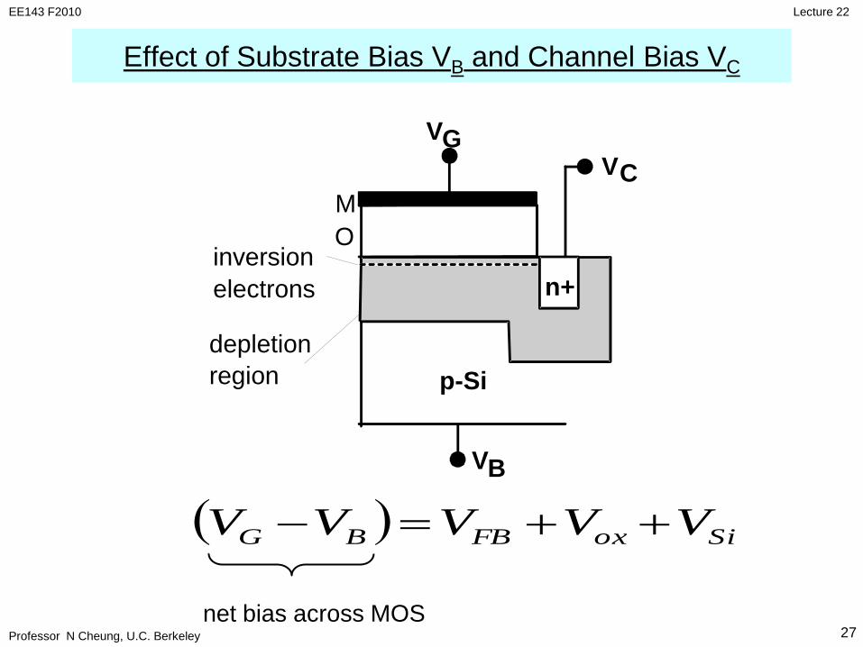
SioxFBBG VVVVV
net bias across MOS
M
O
p-Si
V
VG
C
inversion
electrons
depletion
region
VB
n+n+
Effect of Substrate Bias VB and Channel Bias VC

Professor N Cheung, U.C. Berkeley
Lecture 22EE143 F2010
28
s
da
OX
daFBBG
BCpSi
XqN
C
XqNVVV
VVV
max2
max
2
1
2
M O SiEi
Efs
q(VC-VB)
Efn
pq
pq
s
daSi
XqNV
max2
2
1
At the onset of strong inversion, where VG is defined
as the threshold voltage

Professor N Cheung, U.C. Berkeley
Lecture 22EE143 F2010
29
At threshold: VG – VB = VFB+Vox+VSi
But VSi = 2|p| + (VC - VB ) =>
xdmax is different from no-bias case
B
SiSid
qN
Vx
2max
VT -VB = VFB + 2sqNB(2|F| + VC-VB)
Cox + 2|F| + VC - VB
VoxVSi

Professor N Cheung, U.C. Berkeley
Lecture 22EE143 F2010
30
Flat Band Voltage with Oxide charges
VFB is the Gate voltage required to create no charge in the Si
dxx
xx
CC
QV
oxx
ox
ox
oxox
f
SMFB 0
)(1
x = 0 x = xox
M O S
ox (x)Qf
ox (x) due to alkaline
contaminants or trapped
chargeQf due to broken bonds
at
Si-SiO interface

Professor N Cheung, U.C. Berkeley
Lecture 22EE143 F2010
31
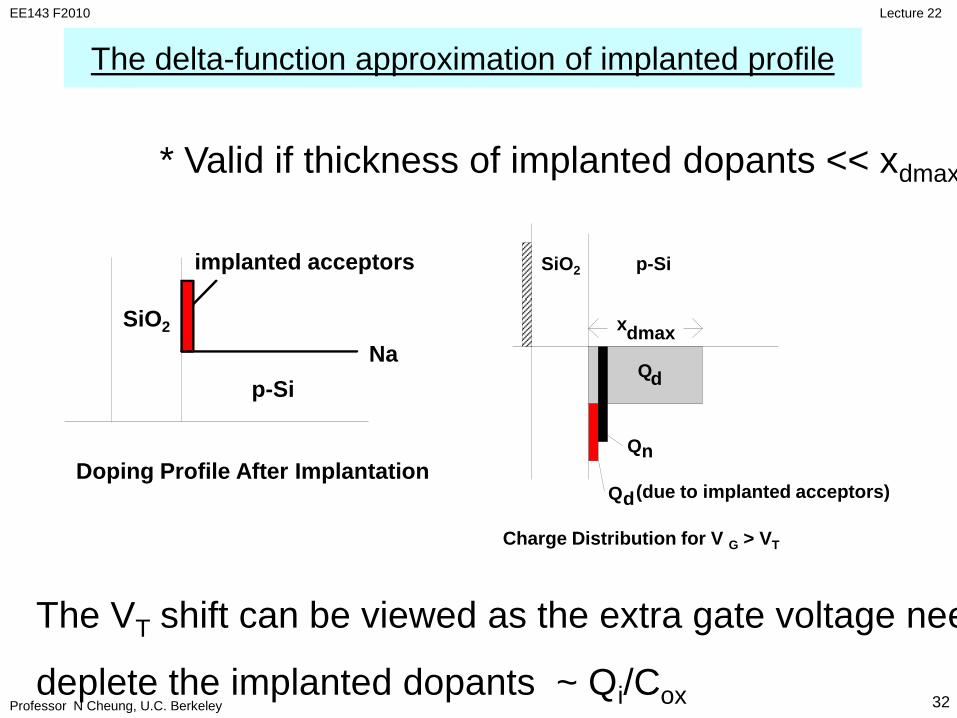
VT Tailoring with Ion Implantation
Nsub
Shallow implanted
dopant profile at Si-SiO2
interface (approximated as
a delta function)
• Acceptor implant gives positive shift (+ VT)
• Donor implant gives negative shift - VT
Algebraic sign of VT shift is independent of n or p substrate !
OX
iT
C
QV
Qi = q implant dose in Si
Professor N Cheung, U.C. Berkeley
Lecture 22EE143 F2010
32
p-Si
implanted acceptors
Na
SiO2
Doping Profile After Implantation
SiO2
xdmax
Q
Qd
d
Qn
p-Si
(due to implanted acceptors)
Charge Distribution for V G > VT
* Valid if thickness of implanted dopants << xdmax
The VT shift can be viewed as the extra gate voltage needed to
deplete the implanted dopants ~ Qi/Cox
The delta-function approximation of implanted profile

Professor N Cheung, U.C. Berkeley
Lecture 22EE143 F2010
33
Summary : Parameters Affecting VT
6
7
n+
Na
VB
5
1
2
4
3
Dopant implant near Si/SiO2 interface
fOX Q& M
xox
VCQn n+

Professor N Cheung, U.C. Berkeley
Lecture 22EE143 F2010
34
+ Qf or Qox
B threshold implant
As or P threshold implant
Xox increases
Xox increases
M increases
M decreases
|VCB| increases
|VCB| increases

Professor N Cheung, U.C. Berkeley
Lecture 22EE143 F2010
35
Summary of MOS Threshold Voltage (NMOS, p-substrate)
• Threshold voltage of MOS capacitor:
• Threshold voltage of MOS transistor:
Note 1: At the onset of strong inversion, inversion charge is negligible
and is often ignored in the VT expression
Note 2: VT of a MOSFET is taken as the VT value at source ( i.e., VC =VS)
Note 3 : Qi = (q implant dose ) is the charge due to the ionized donors
or acceptors implanted at the Si surface. Qi is negative for acceptors
and is positive for donors
VT = VFB + 2sqNB(2|F|)
Cox + 2|F| -
Qi
Cox
VT = VFB + 2sqNB(2|F| + |VC-VB|)
Cox + 2|F| + VC -
Qi
Cox
Professor N Cheung, U.C. Berkeley
Lecture 22EE143 F2010
36
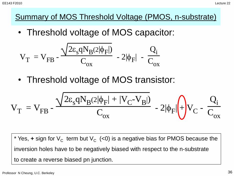
Summary of MOS Threshold Voltage (PMOS, n-substrate)
• Threshold voltage of MOS capacitor:
• Threshold voltage of MOS transistor:
* Yes, + sign for VC term but VC (<0) is a negative bias for PMOS because the
inversion holes have to be negatively biased with respect to the n-substrate
to create a reverse biased pn junction.
VT = VFB - 2sqNB(2|F|)
Cox - 2|F| -
Qi
Cox
VT = VFB - 2sqNB(2|F| + |VC-VB|)
Cox - 2|F| + VC -
Qi
Cox