EE115C Winter 2017 Digital Electronic...
32
EE115C – Winter 2017 Digital Electronic Circuits Lecture 17: Latches and Flip-Flops
Transcript of EE115C Winter 2017 Digital Electronic...
EE115C – Winter 2017Digital Electronic Circuits
Lecture 17:
Latches and Flip-Flops
EE115C – Winter 2017 2
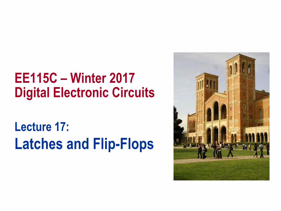
COMBINATIONALLOGIC
Registers
Outputs
Next state
CLK
Q D
Current State
Inputs
Sequential Logic
2 storage mechanisms– Positive feedback
– Charge based
EE115C – Winter 2017 3
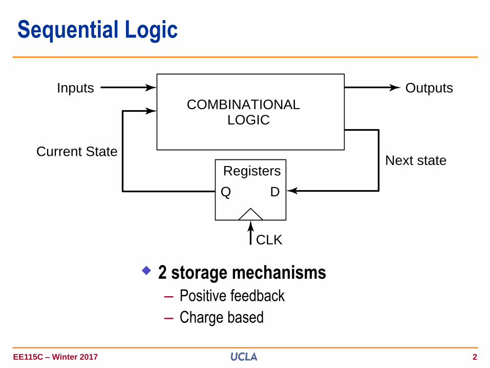
Latch versus Flip-Flop
D
Clk
Q D
Clk
Q
Flip-flop: edge-triggered
stores data when
clock rises
Clk Clk
D D
Q Q
Latch: level-sensitive
clock is low – hold mode
clock is high – transparent
EE115C – Winter 2017 4
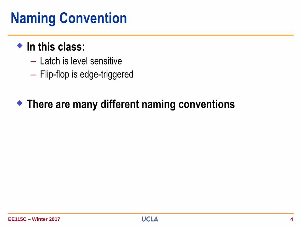
Naming Convention
In this class:– Latch is level sensitive
– Flip-flop is edge-triggered
There are many different naming conventions
EE115C – Winter 2017 5
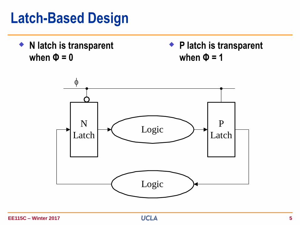
N
LatchLogic
Logic
P
Latch
Latch-Based Design
N latch is transparent
when Φ = 0
P latch is transparent
when Φ = 1
EE115C – Winter 2017 6
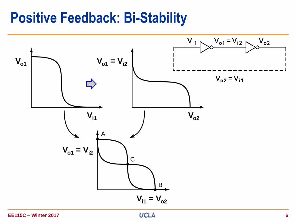
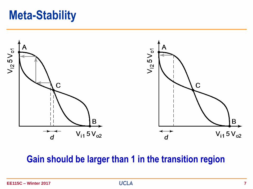
A
C
B
Positive Feedback: Bi-Stability
Vo1
Vi1
Vi1 = Vo2
Vo2
Vo1 = Vi2
Vo1 = Vi2
EE115C – Winter 2017 7
Gain should be larger than 1 in the transition region
Meta-Stability
EE115C – Winter 2017 8
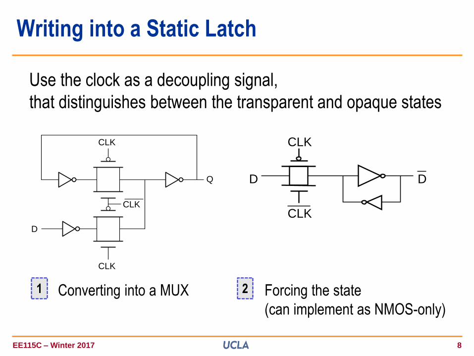
Writing into a Static Latch
CLK
CLK
CLK
D
Q D
CLK
CLK
D
Converting into a MUX Forcing the state
(can implement as NMOS-only)
Use the clock as a decoupling signal,
that distinguishes between the transparent and opaque states
1 2
EE115C – Winter 2017 9
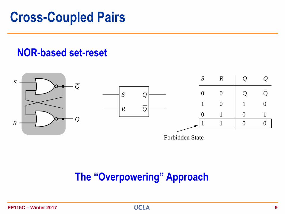
Cross-Coupled Pairs
Forbidden State
S
S
R
Q
Q
Q
QRS Q
Q00 Q
101 0
010 1
011 0RQ
NOR-based set-reset
The “Overpowering” Approach
EE115C – Winter 2017 10
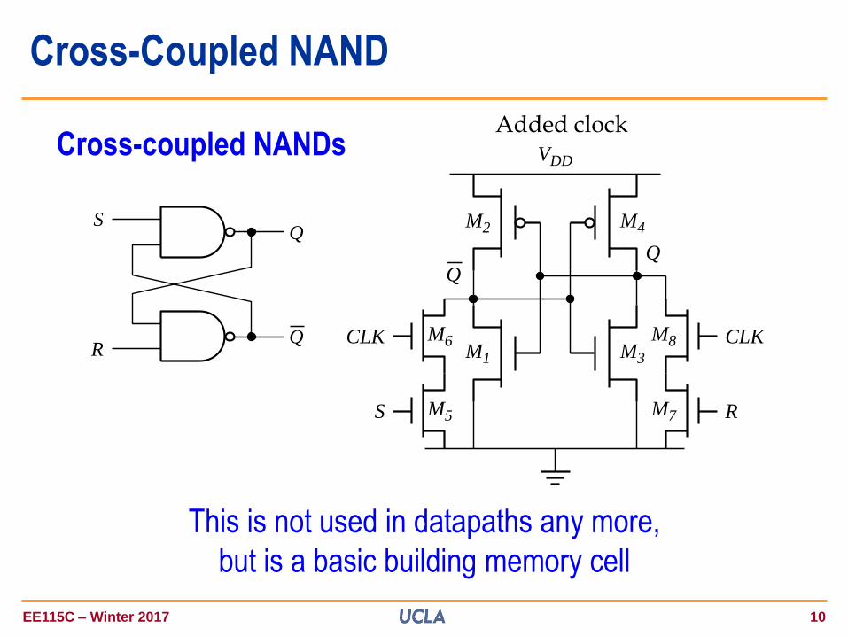
Cross-Coupled NAND
S
QR
Q
M1
M2
M3
M4
Q
M5S
M6CLK
M7 R
M8 CLK
VDD
Q
Cross-coupled NANDsAdded clock
This is not used in datapaths any more,
but is a basic building memory cell
EE115C – Winter 2017 11
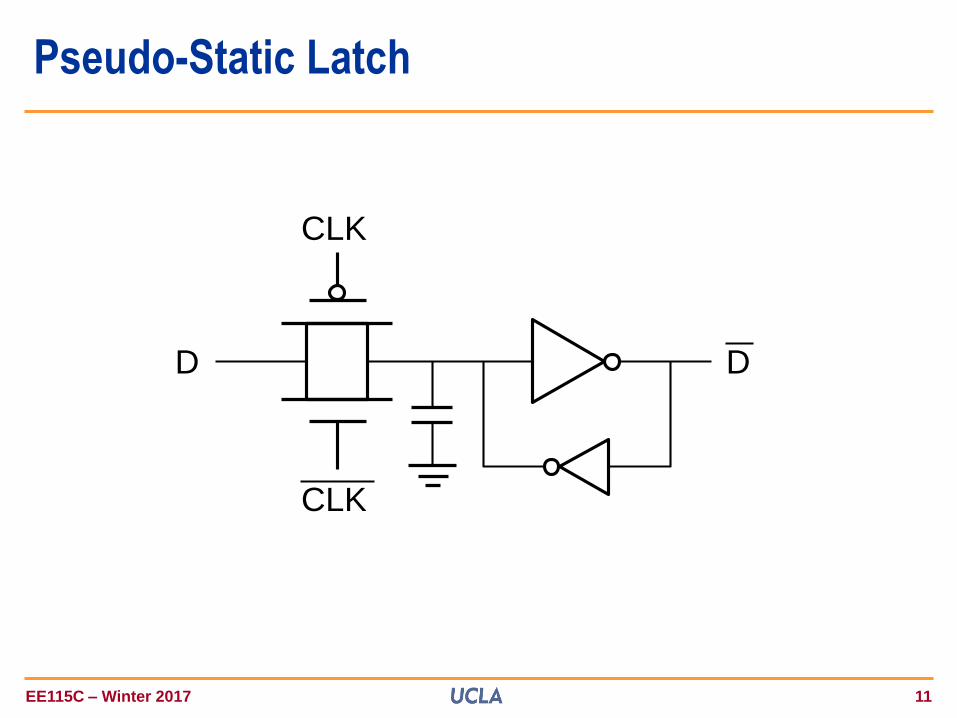
Pseudo-Static Latch
D
CLK
CLK
D
EE115C – Winter 2017 12
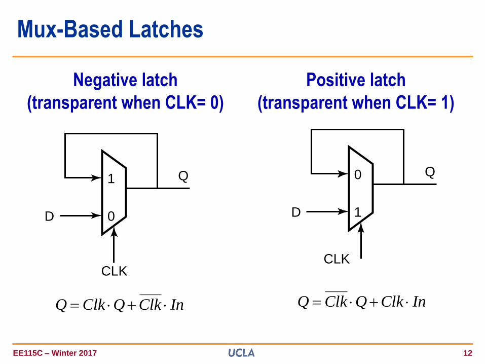
Mux-Based Latches
Negative latch
(transparent when CLK= 0)
Positive latch
(transparent when CLK= 1)
CLK
1
0D
Q 0
CLK
1D
Q
InClkQClkQ InClkQClkQ
EE115C – Winter 2017 13
CLK
CLK
CLK
D
Q
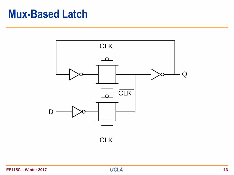
Mux-Based Latch
EE115C – Winter 2017 14
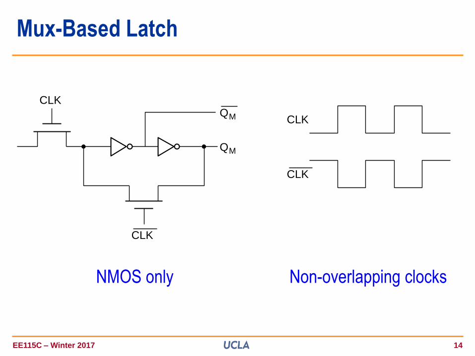
Mux-Based Latch
CLK
CLK
CLK
CLK
QM
QM
NMOS only Non-overlapping clocks
EE115C – Winter 2017 15
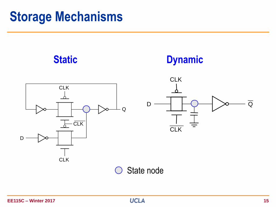
Storage Mechanisms
D
CLK
CLK
Q
Dynamic
CLK
CLK
CLK
D
Q
Static
State node
EE115C – Winter 2017 16
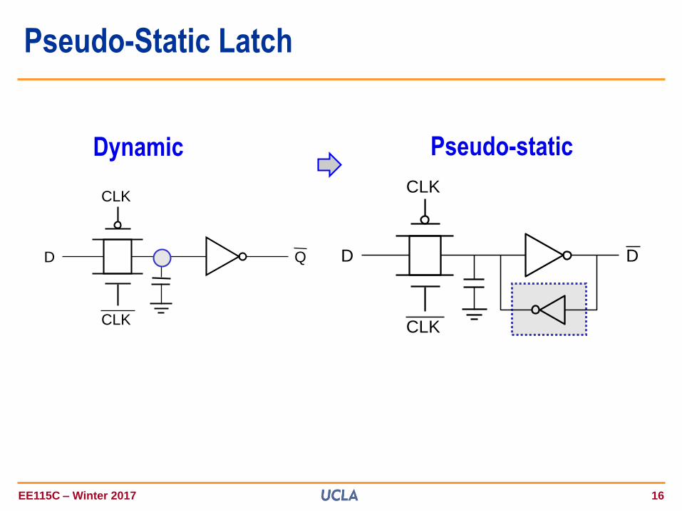
Pseudo-Static Latch
D
CLK
CLK
DD
CLK
CLK
Q
Dynamic Pseudo-static
EE115C – Winter 2017 17
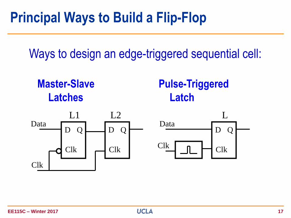
Principal Ways to Build a Flip-Flop
Master-Slave
Latches
D
Clk
Q D
Clk
Q
Clk
DataD
Clk
Q
Clk
Data
Pulse-Triggered
Latch
L1 L2 L
Ways to design an edge-triggered sequential cell:
EE115C – Winter 2017 18
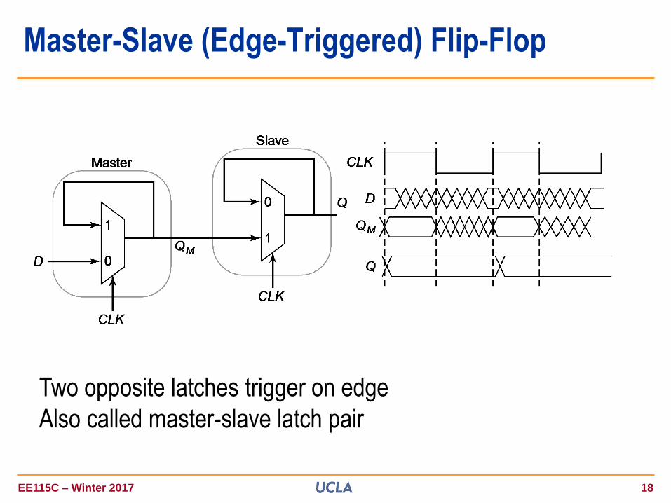
Two opposite latches trigger on edge
Also called master-slave latch pair
Master-Slave (Edge-Triggered) Flip-Flop
EE115C – Winter 2017 19
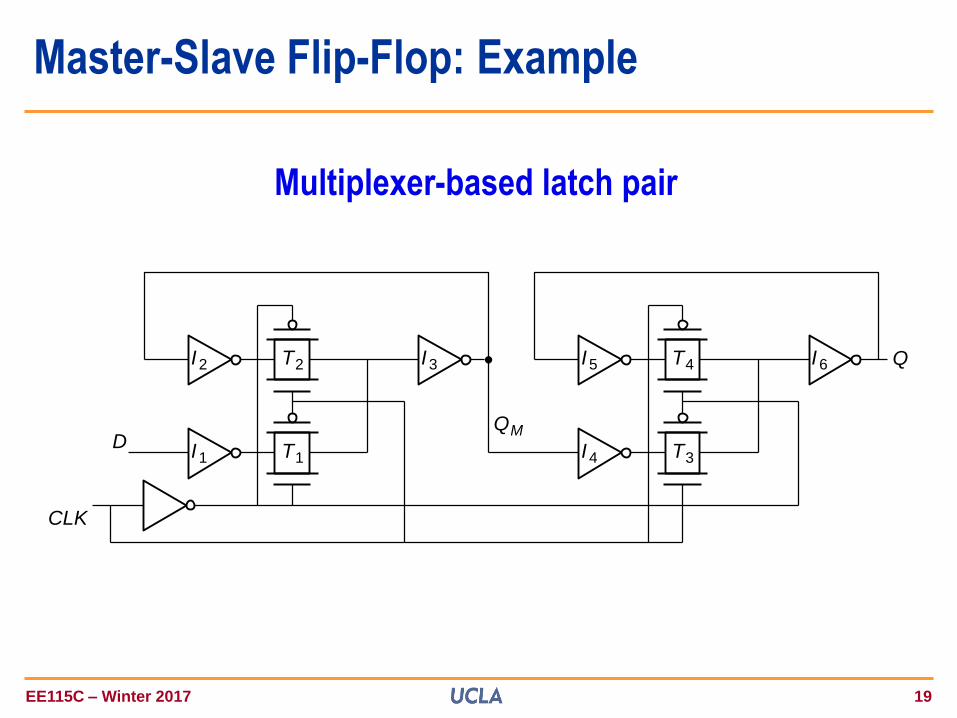
Master-Slave Flip-Flop: Example
QM
Q
D
CLK
T2I2
T1I1
I3 T4I5
T3I4
I6
Multiplexer-based latch pair
EE115C – Winter 2017 20
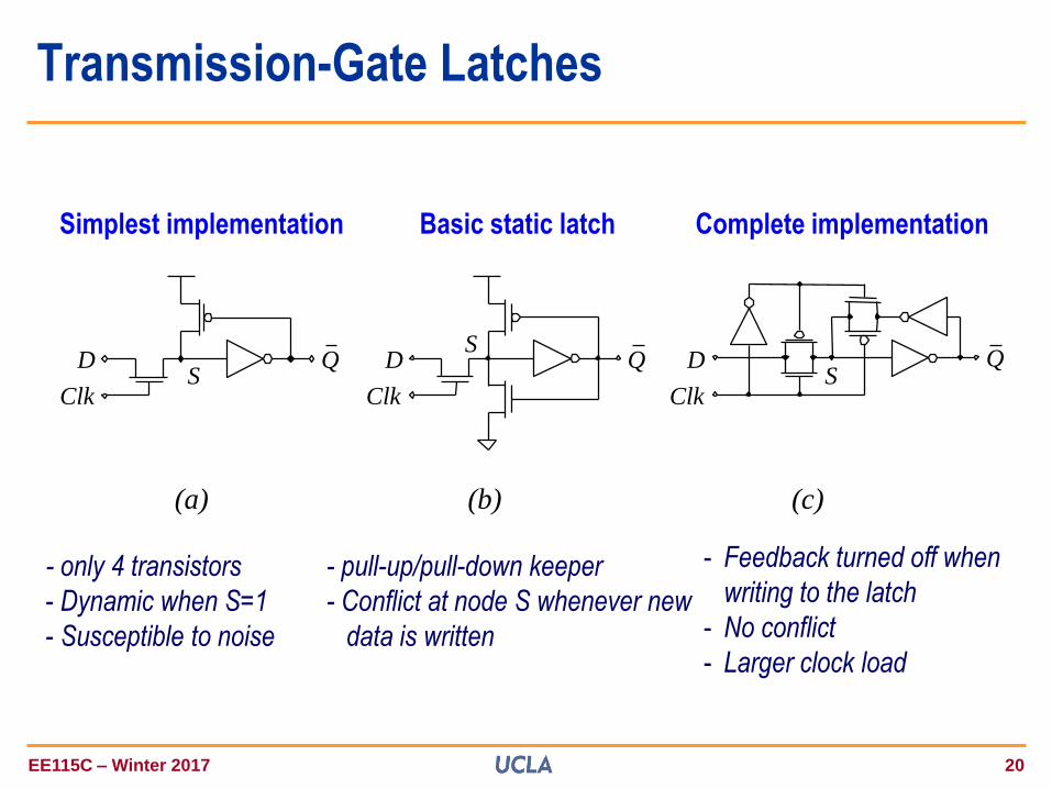
Simplest implementation Basic static latch Complete implementation
- only 4 transistors
- Dynamic when S=1
- Susceptible to noise
- pull-up/pull-down keeper
- Conflict at node S whenever new
data is written
- Feedback turned off when
writing to the latch
- No conflict
- Larger clock load
(a) (c)
Clk
D Q QS
(b)
QS
SClk
D
Clk
D
Transmission-Gate Latches
EE115C – Winter 2017 21
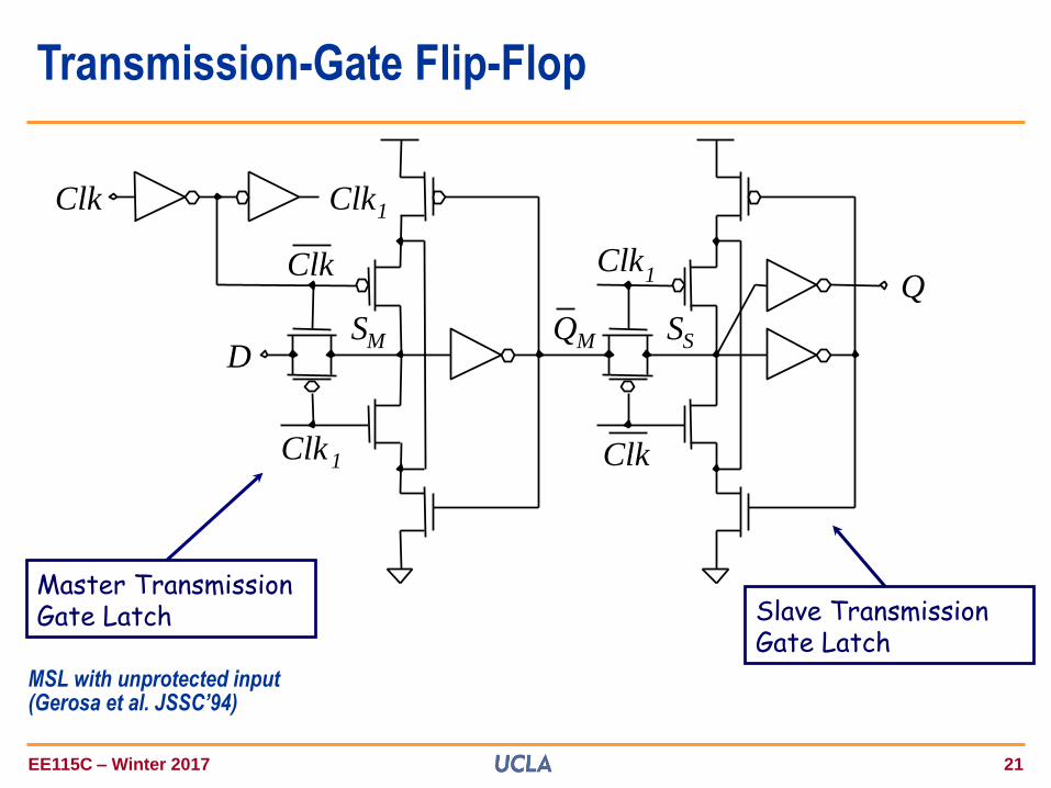
MSL with unprotected input(Gerosa et al. JSSC’94)
Master Transmission Gate Latch Slave Transmission
Gate Latch
D
Q
Clk Clk1
Clk
QMSM SS
Clk1
Clk1
Clk
Transmission-Gate Flip-Flop
EE115C – Winter 2017 22
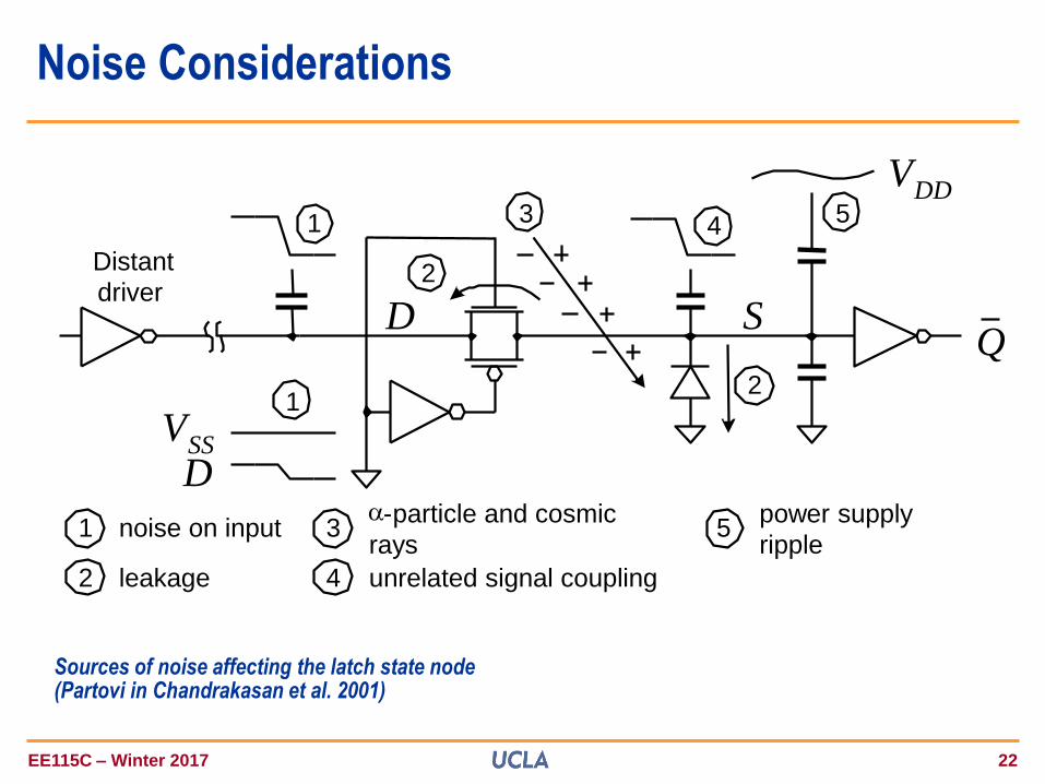
Sources of noise affecting the latch state node(Partovi in Chandrakasan et al. 2001)
D
2
3
2
1
Distant
driver
4 5
1
DV
SS
VDD
QS
1 noise on input
2 leakage
3a-particle and cosmic
rays
4 unrelated signal coupling
5power supply
ripple
Noise Considerations
EE115C – Winter 2017 23
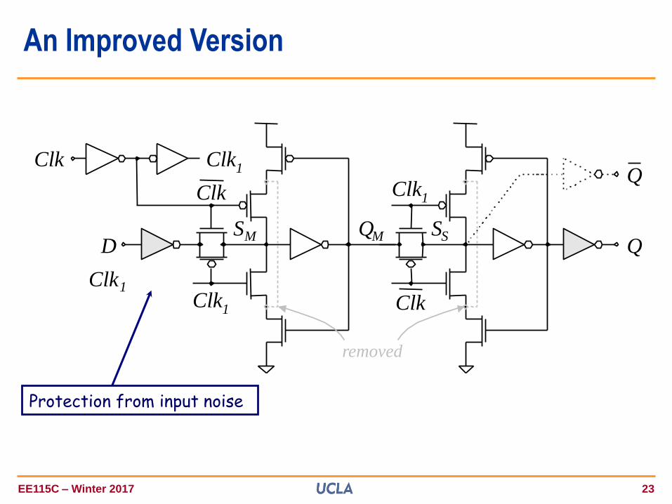
Protection from input noise
D
Q
SM SSQ
Clk1
Clk
Clk Clk1
Clk1
Clk
QM
Clk1
removed
An Improved Version
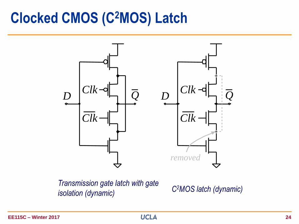
EE115C – Winter 2017 24
Transmission gate latch with gate
isolation (dynamic)C2MOS latch (dynamic)
Clocked CMOS (C2MOS) Latch
D DClk
Clk
Q QClk
Clk
removed
EE115C – Winter 2017 25
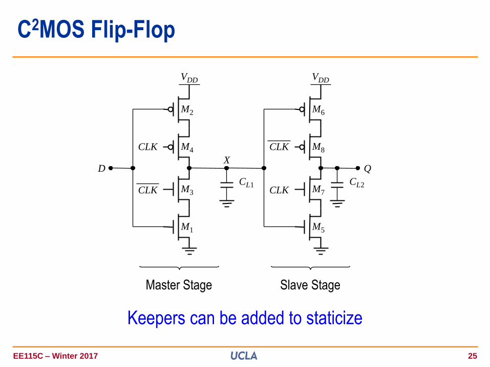
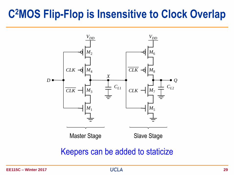
Keepers can be added to staticize
M1
D Q
M3CLK
M4
M2
CLK
VDD
CL1
X
CL2
Master Stage
M5
M7CLK
CLK M8
M6
VDD
Slave Stage
C2MOS Flip-Flop
EE115C – Winter 2017 26
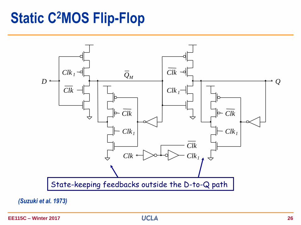
(Suzuki et al. 1973)
State-keeping feedbacks outside the D-to-Q path
D Q
Clk1
Clk
Clk
Clk 1
Clk
Clk1
Clk
QMClk
Clk 1
Clk1
Clk
Static C2MOS Flip-Flop
EE115C – Winter 2017 27
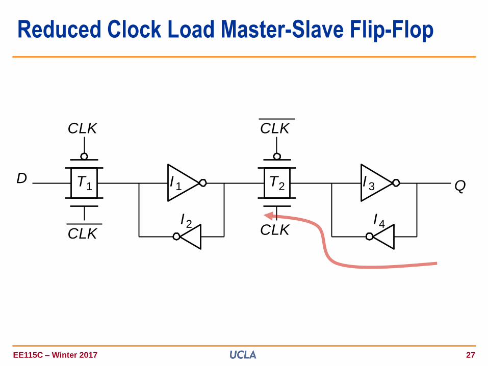
DQT1 I 1
CLK
CLK
T2
CLK
CLKI2
I 3
I4
Reduced Clock Load Master-Slave Flip-Flop
EE115C – Winter 2017 28
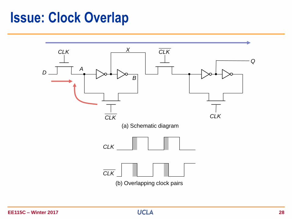
Issue: Clock Overlap
CLK
CLK
A
B
(a) Schematic diagram
(b) Overlapping clock pairs
X
D
Q
CLK
CLK
CLK
CLK
EE115C – Winter 2017 29
Keepers can be added to staticize
M1
D Q
M3CLK
M4
M2
CLK
VDD
CL1
X
CL2
Master Stage
M5
M7CLK
CLK M8
M6
VDD
Slave Stage
C2MOS Flip-Flop is Insensitive to Clock Overlap
EE115C – Winter 2017 30
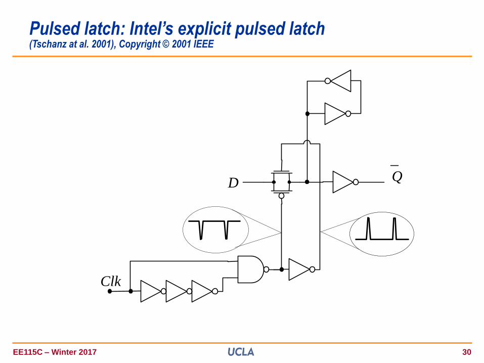
Pulsed latch: Intel’s explicit pulsed latch(Tschanz at al. 2001), Copyright © 2001 IEEE
D Q
Clk
EE115C – Winter 2017 31
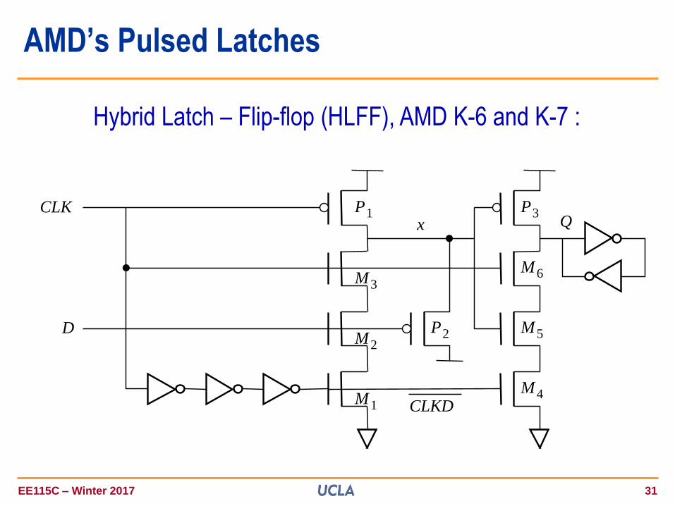
AMD’s Pulsed Latches
Hybrid Latch – Flip-flop (HLFF), AMD K-6 and K-7 :
P1
M3
M2
D
CLK
M1
P3
M6
Qx
M5
M4
P2
CLKD
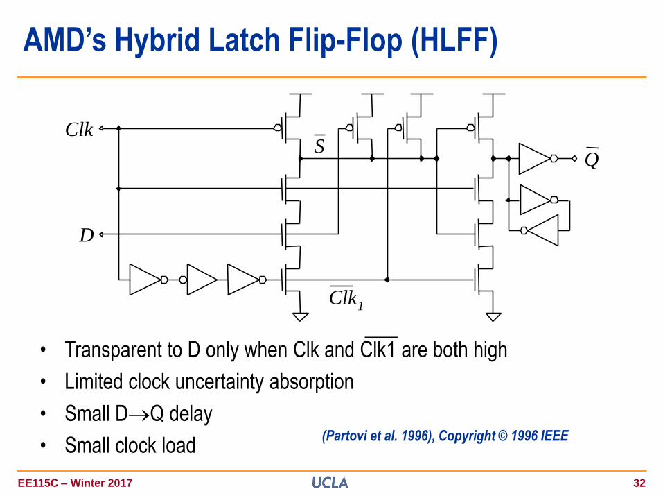
EE115C – Winter 2017 32
(Partovi et al. 1996), Copyright © 1996 IEEE
• Transparent to D only when Clk and Clk1 are both high
• Limited clock uncertainty absorption
• Small DQ delay
• Small clock load
D
Q
ClkS
Clk1
AMD’s Hybrid Latch Flip-Flop (HLFF)