
EE 447 VLSI Design Lecture 5: Wires. EE 447VLSI Design 6: Wires2 Outline Introduction Wire...
36
EE 447 VLSI Design Lecture 5: Wires
-
Upload
sharyl-dalton -
Category
Documents
-
view
217 -
download
0
Transcript of EE 447 VLSI Design Lecture 5: Wires. EE 447VLSI Design 6: Wires2 Outline Introduction Wire...
EE 447 VLSI Design
Lecture 5: Wires
6: Wires 2EE 447VLSI Design
Outline
Introduction Wire Resistance Wire Capacitance Wire RC Delay Crosstalk Wire Engineering Repeaters
6: Wires 3EE 447VLSI Design
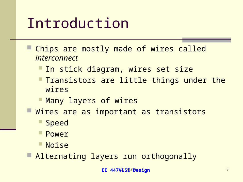
Introduction
Chips are mostly made of wires called interconnect In stick diagram, wires set size Transistors are little things under the wires Many layers of wires
Wires are as important as transistors Speed Power Noise
Alternating layers run orthogonally
6: Wires 4EE 447VLSI Design
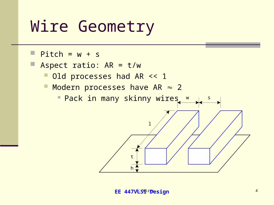
Wire Geometry
Pitch = w + s Aspect ratio: AR = t/w
Old processes had AR << 1 Modern processes have AR 2
Pack in many skinny wires
l
w s
t
h
6: Wires 5EE 447VLSI Design
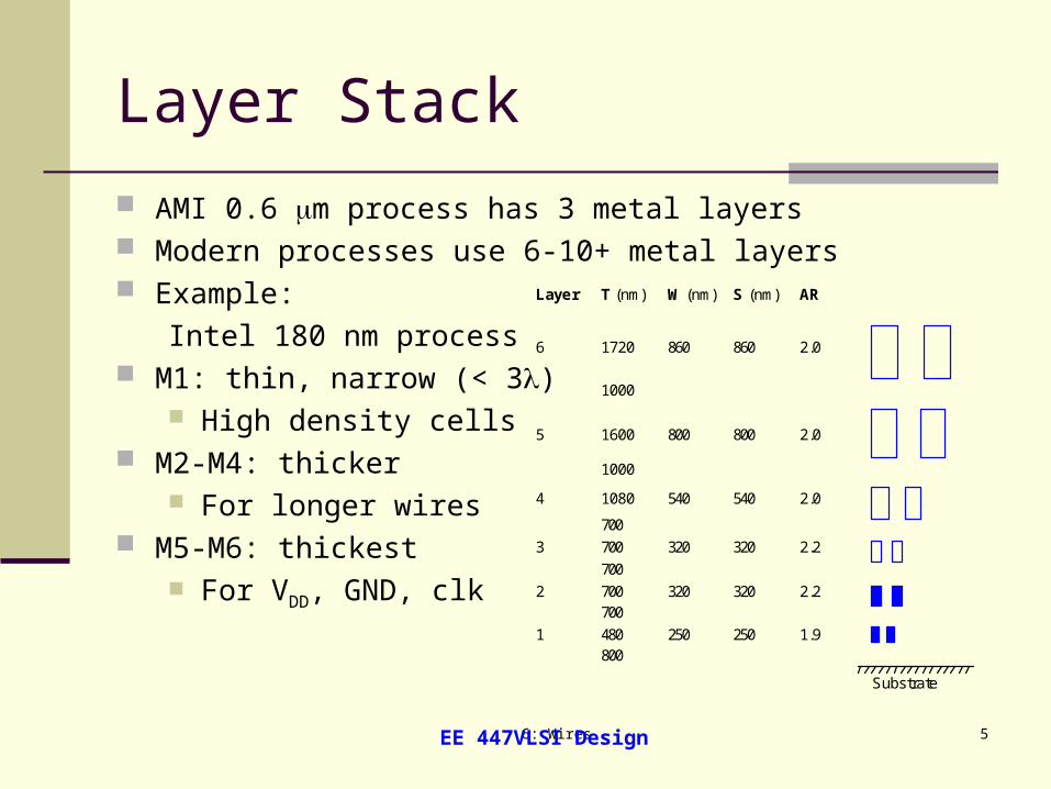
Layer Stack
AMI 0.6 m process has 3 metal layers Modern processes use 6-10+ metal layers Example:
Intel 180 nm process M1: thin, narrow (< 3)
High density cells M2-M4: thicker
For longer wires M5-M6: thickest
For VDD, GND, clk
Layer T (nm) W (nm) S (nm) AR
6 1720 860 860 2.0
1000
5 1600 800 800 2.0
1000
4 1080 540 540 2.0
700
3 700 320 320 2.2
700
2 700 320 320 2.2700
1 480 250 250 1.9800
Substrate
6: Wires 6EE 447VLSI Design
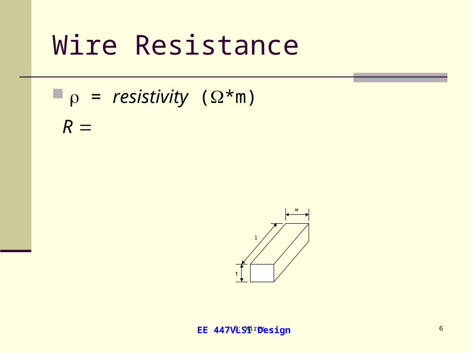
Wire Resistance
= resistivity (*m)
l
w
t
R
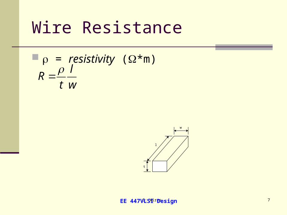
6: Wires 7EE 447VLSI Design
Wire Resistance
= resistivity (*m)
l
w
t
lR
t w
6: Wires 8EE 447VLSI Design
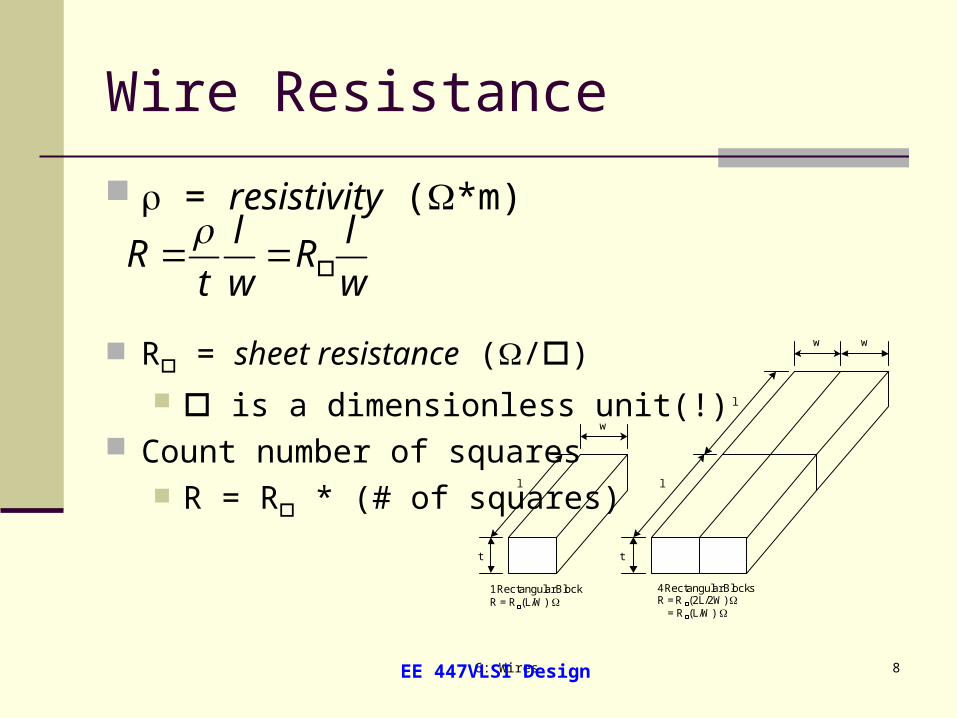
Wire Resistance
= resistivity (*m)
R = sheet resistance (/) is a dimensionless unit(!)
Count number of squares R = R * (# of squares)
l
w
t
1 Rectangular BlockR = R (L/W)
4 Rectangular BlocksR = R (2L/2W) = R (L/W)
t
l
w w
l
l lR R
t w w
6: Wires 9EE 447VLSI Design
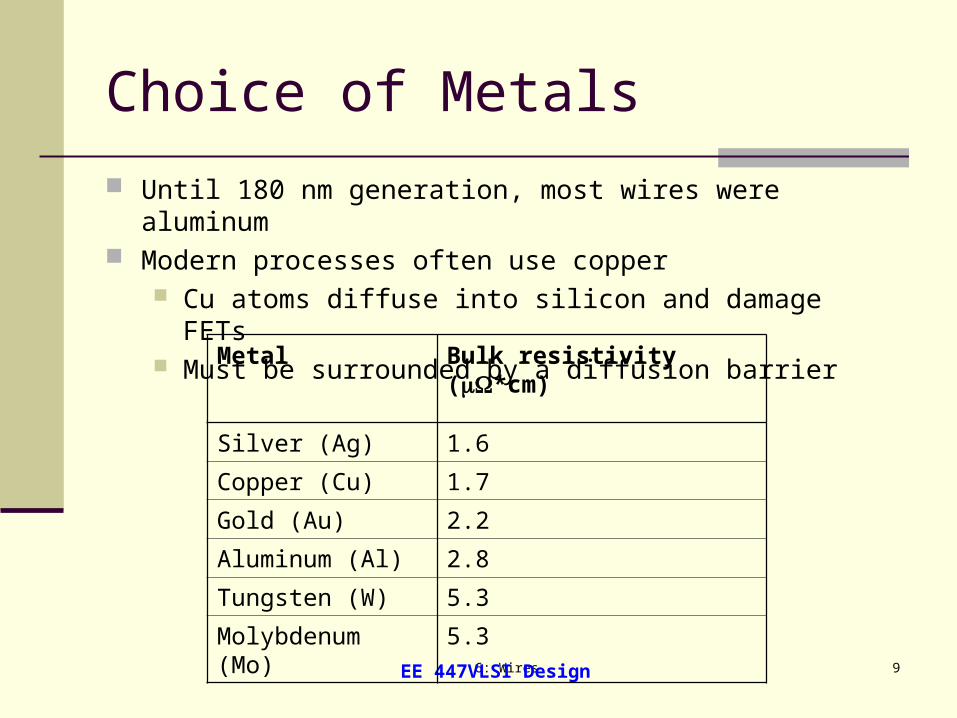
Choice of Metals
Until 180 nm generation, most wires were aluminum Modern processes often use copper
Cu atoms diffuse into silicon and damage FETs Must be surrounded by a diffusion barrier
Metal Bulk resistivity (*cm)
Silver (Ag) 1.6
Copper (Cu) 1.7
Gold (Au) 2.2
Aluminum (Al) 2.8
Tungsten (W) 5.3
Molybdenum (Mo) 5.3
6: Wires 10EE 447VLSI Design
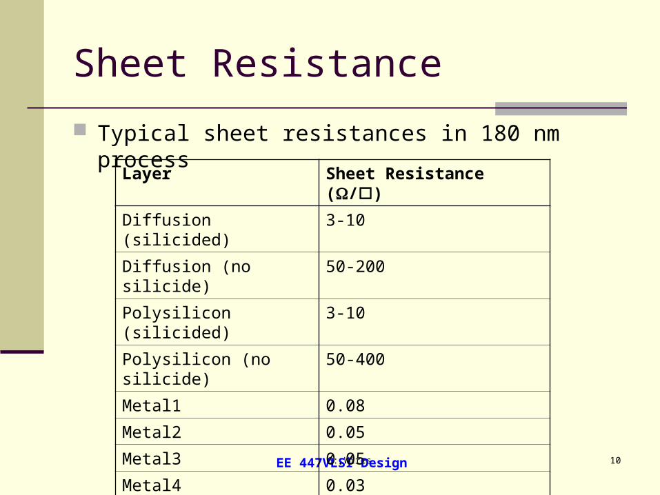
Sheet Resistance
Typical sheet resistances in 180 nm process
Layer Sheet Resistance (/)
Diffusion (silicided) 3-10
Diffusion (no silicide) 50-200
Polysilicon (silicided) 3-10
Polysilicon (no silicide) 50-400
Metal1 0.08
Metal2 0.05
Metal3 0.05
Metal4 0.03
Metal5 0.02
Metal6 0.02
6: Wires 11EE 447VLSI Design
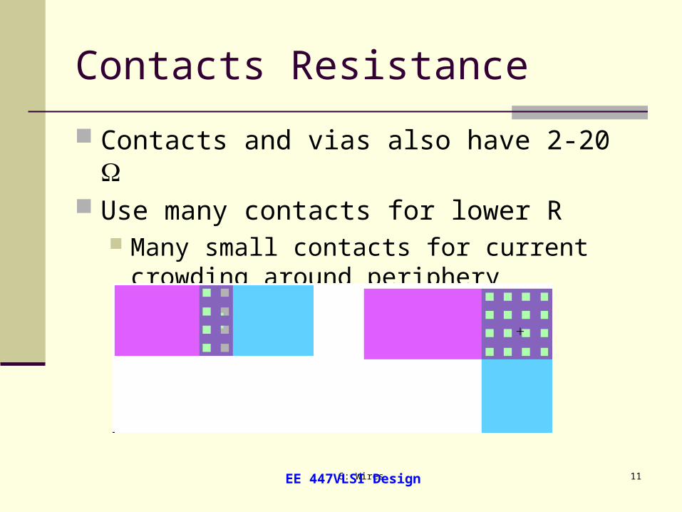
Contacts Resistance
Contacts and vias also have 2-20 Use many contacts for lower R
Many small contacts for current crowding around periphery
6: Wires 12EE 447VLSI Design
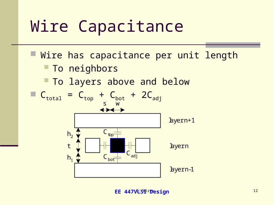
Wire Capacitance
Wire has capacitance per unit length To neighbors To layers above and below
Ctotal = Ctop + Cbot + 2Cadj
layer n+1
layer n
layer n-1
Cadj
Ctop
Cbot
ws
t
h1
h2
6: Wires 13EE 447VLSI Design
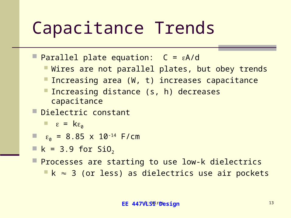
Capacitance Trends
Parallel plate equation: C = A/d Wires are not parallel plates, but obey trends Increasing area (W, t) increases capacitance Increasing distance (s, h) decreases capacitance
Dielectric constant = k0
0 = 8.85 x 10⁻¹⁴ F/cm
k = 3.9 for SiO2
Processes are starting to use low-k dielectrics k 3 (or less) as dielectrics use air pockets
6: Wires 14EE 447VLSI Design
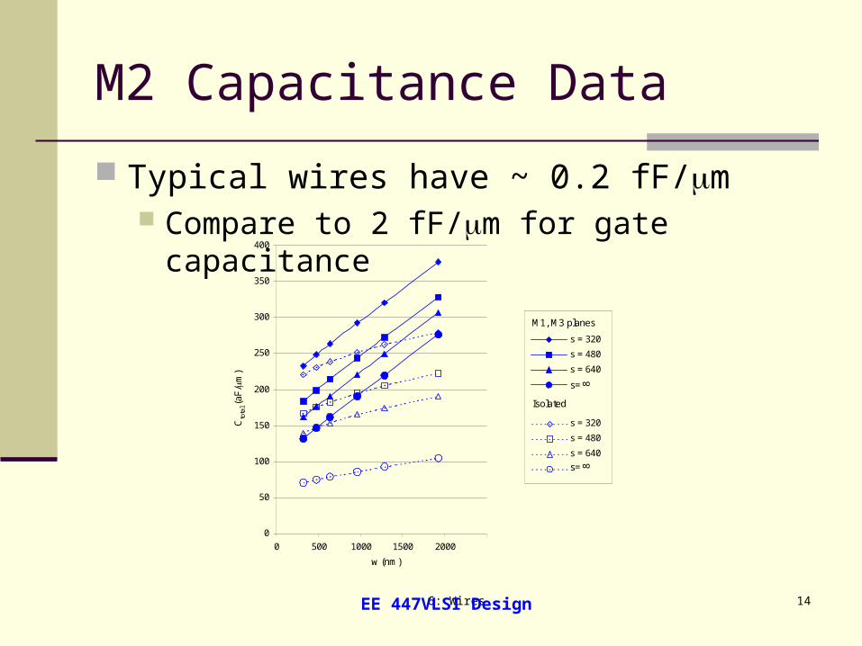
M2 Capacitance Data
Typical wires have ~ 0.2 fF/m Compare to 2 fF/m for gate capacitance
0
50
100
150
200
250
300
350
400
0 500 1000 1500 2000
Cto
tal (
aF/
m)
w (nm)
Isolated
M1, M3 planes
s = 320
s = 480
s = 640
s= 8
s = 320
s = 480
s = 640
s= 8
6: Wires 15EE 447VLSI Design
Diffusion & Polysilicon
Diffusion capacitance is very high (about 2 fF/m) Comparable to gate capacitance Diffusion also has high resistance Avoid using diffusion runners for wires!
Polysilicon has lower C but high R Use for transistor gates Occasionally for very short wires between
gates
6: Wires 16EE 447VLSI Design
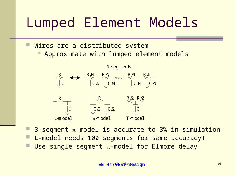
Lumped Element Models
Wires are a distributed system Approximate with lumped element models
3-segment -model is accurate to 3% in simulation L-model needs 100 segments for same accuracy! Use single segment -model for Elmore delay
C
R
C/N
R/N
C/N
R/N
C/N
R/N
C/N
R/N
R
C
L-model
R
C/2 C/2
R/2 R/2
C
N segments
-model T-model
6: Wires 17EE 447VLSI Design
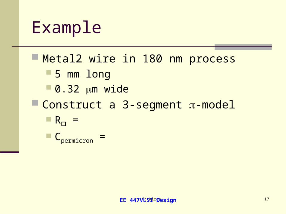
Example
Metal2 wire in 180 nm process 5 mm long 0.32 m wide
Construct a 3-segment -model R =
Cpermicron =
6: Wires 18EE 447VLSI Design
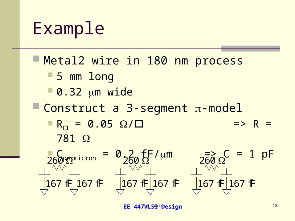
Example
Metal2 wire in 180 nm process 5 mm long 0.32 m wide
Construct a 3-segment -model R = 0.05 / => R = 781 Cpermicron = 0.2 fF/m => C = 1 pF
260
167 fF 167 fF
260
167 fF 167 fF
260
167 fF 167 fF
6: Wires 19EE 447VLSI Design
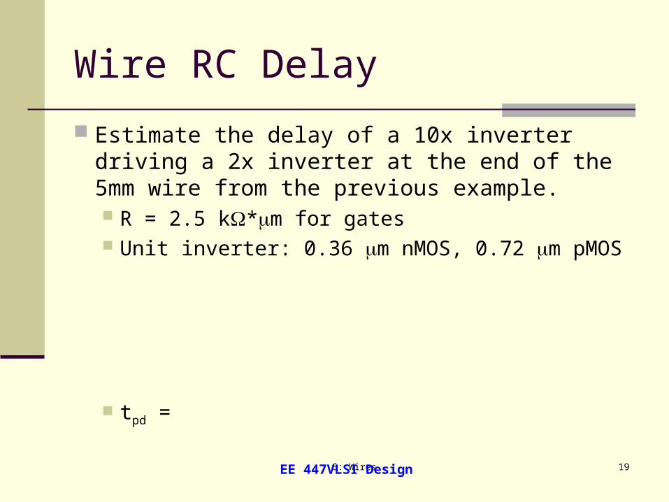
Wire RC Delay
Estimate the delay of a 10x inverter driving a 2x inverter at the end of the 5mm wire from the previous example. R = 2.5 k*m for gates Unit inverter: 0.36 m nMOS, 0.72 m pMOS
tpd =

6: Wires 20EE 447VLSI Design
Wire RC Delay
Estimate the delay of a 10x inverter driving a 2x inverter at the end of the 5mm wire from the previous example. R = 2.5 k*m for gates Unit inverter: 0.36 m nMOS, 0.72 m pMOS
tpd = 1.1 ns
781
500 fF 500 fF
Driver Wire
4 fF
Load
690
6: Wires 21EE 447VLSI Design
Crosstalk
A capacitor does not like to change its voltage instantaneously.
A wire has high capacitance to its neighbor. When the neighbor switches from 1-> 0 or 0-
>1, the wire tends to switch too. Called capacitive coupling or crosstalk.
Crosstalk effects Noise on nonswitching wires Increased delay on switching wires
6: Wires 22EE 447VLSI Design
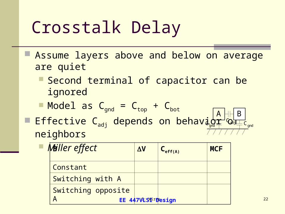
Crosstalk Delay
Assume layers above and below on average are quiet Second terminal of capacitor can be ignored Model as Cgnd = Ctop + Cbot
Effective Cadj depends on behavior of neighbors Miller effect A B
CadjCgnd Cgnd
B V Ceff(A) MCF
Constant
Switching with A
Switching opposite A
6: Wires 23EE 447VLSI Design
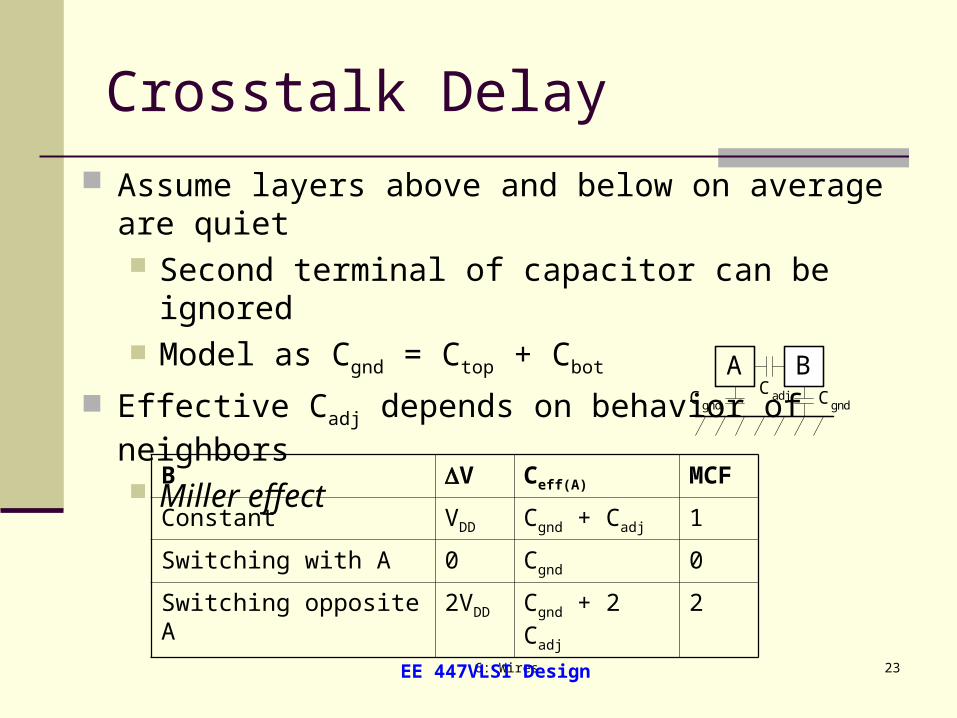
Crosstalk Delay
Assume layers above and below on average are quiet Second terminal of capacitor can be ignored Model as Cgnd = Ctop + Cbot
Effective Cadj depends on behavior of neighbors Miller effect A B
CadjCgnd Cgnd
B V Ceff(A) MCF
Constant VDD Cgnd + Cadj 1
Switching with A 0 Cgnd 0
Switching opposite A 2VDD Cgnd + 2 Cadj 2
6: Wires 24EE 447VLSI Design
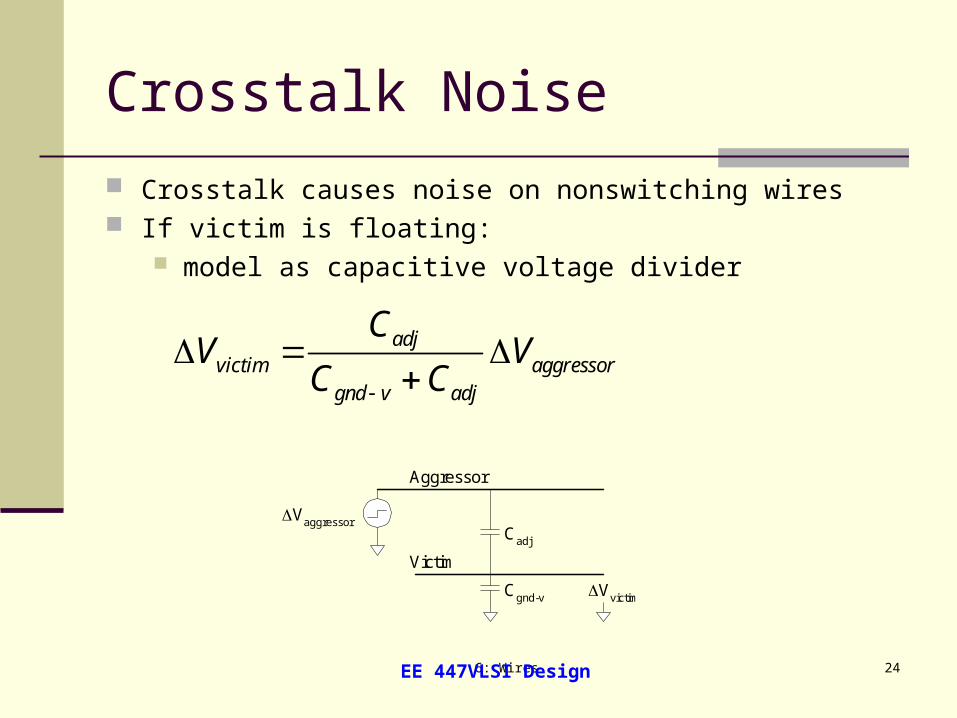
Crosstalk Noise
Crosstalk causes noise on nonswitching wires If victim is floating:
model as capacitive voltage divider
Cadj
Cgnd-v
Aggressor
Victim
Vaggressor
Vvictim
adjvictim aggressor
gnd v adj
CV V
C C
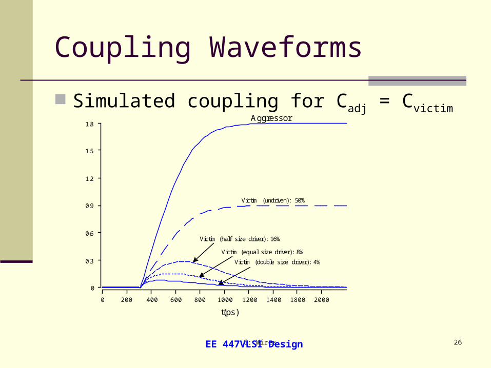
6: Wires 25EE 447VLSI Design
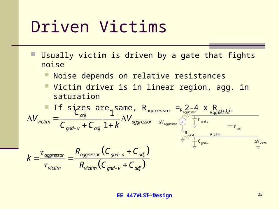
Driven Victims
Usually victim is driven by a gate that fights noise Noise depends on relative resistances Victim driver is in linear region, agg. in saturation If sizes are same, Raggressor = 2-4 x Rvictim
1
1adj
victim aggressorgnd v adj
CV V
C C k
aggressor gnd a adjaggressor
victim victim gnd v adj
R C Ck
R C C
Cadj
Cgnd-v
Aggressor
Victim
Vaggressor
Vvictim
Raggressor
Rvictim
Cgnd-a
6: Wires 26EE 447VLSI Design
Coupling Waveforms
Aggressor
Victim (undriven): 50%
Victim (half size driver): 16%
Victim (equal size driver): 8%
Victim (double size driver): 4%
t (ps)
0 200 400 600 800 1000 1200 1400 1800 2000
0
0.3
0.6
0.9
1.2
1.5
1.8
Simulated coupling for Cadj = Cvictim
6: Wires 27EE 447VLSI Design
Noise Implications
So what if we have noise? If the noise is less than the noise margin, nothing
happens Static CMOS logic will eventually settle to correct
output even if disturbed by large noise spikes But glitches cause extra delay Also cause extra power from false transitions
Dynamic logic never recovers from glitches Memories and other sensitive circuits also can
produce the wrong answer
6: Wires 28EE 447VLSI Design
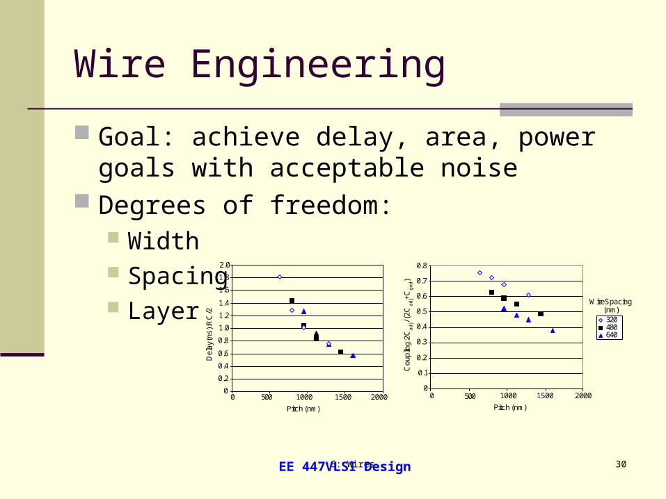
Wire Engineering
Goal: achieve delay, area, power goals with acceptable noise
Degrees of freedom:
6: Wires 29EE 447VLSI Design
Wire Engineering
Goal: achieve delay, area, power goals with acceptable noise
Degrees of freedom: Width Spacing
Del
ay (n
s): R
C/2
Wire Spacing(nm)
Cou
plin
g: 2C
ad
j / (2
Ca
dj+
Cg
nd)
0
0.2
0.4
0.6
0.8
1.0
1.2
1.4
1.6
1.8
2.0
0 500 1000 1500 20000
0.1
0.2
0.3
0.4
0.5
0.6
0.7
0.8
0 500 1000 1500 2000
320480640
Pitch (nm)Pitch (nm)
6: Wires 30EE 447VLSI Design
Wire Engineering
Goal: achieve delay, area, power goals with acceptable noise
Degrees of freedom: Width Spacing Layer
Del
ay (n
s): R
C/2
Wire Spacing(nm)
Cou
plin
g: 2C
ad
j / (2
Ca
dj+
Cg
nd)
0
0.2
0.4
0.6
0.8
1.0
1.2
1.4
1.6
1.8
2.0
0 500 1000 1500 20000
0.1
0.2
0.3
0.4
0.5
0.6
0.7
0.8
0 500 1000 1500 2000
320480640
Pitch (nm)Pitch (nm)
6: Wires 31EE 447VLSI Design
Wire Engineering
Goal: achieve delay, area, power goals with acceptable noise
Degrees of freedom: Width Spacing Layer Shielding
Del
ay (n
s): R
C/2
Wire Spacing(nm)
Cou
plin
g: 2C
ad
j / (2
Ca
dj+
Cg
nd)
0
0.2
0.4
0.6
0.8
1.0
1.2
1.4
1.6
1.8
2.0
0 500 1000 1500 20000
0.1
0.2
0.3
0.4
0.5
0.6
0.7
0.8
0 500 1000 1500 2000
320480640
Pitch (nm)Pitch (nm)
vdd a0a1gnd a2vdd b0 a1 a2 b2vdd a0 a1 gnd a2 a3 vdd gnd a0 b1
6: Wires 32EE 447VLSI Design
Repeaters
R and C are proportional to l RC delay is proportional to l2
Unacceptably great for long wires
6: Wires 33EE 447VLSI Design
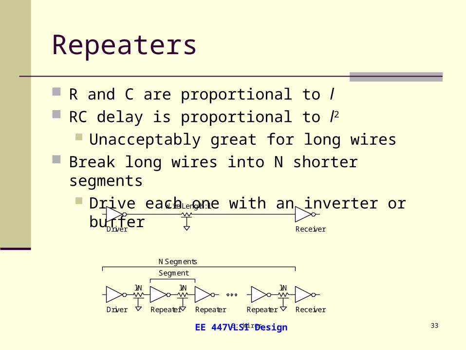
Repeaters
R and C are proportional to l RC delay is proportional to l2
Unacceptably great for long wires Break long wires into N shorter segments
Drive each one with an inverter or bufferWire Length: l
Driver Receiver
l/N
Driver
Segment
Repeater
l/N
Repeater
l/N
ReceiverRepeater
N Segments
6: Wires 34EE 447VLSI Design
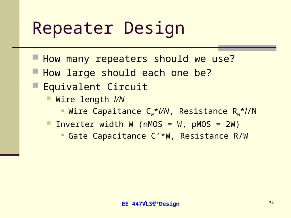
Repeater Design
How many repeaters should we use? How large should each one be? Equivalent Circuit
Wire length l/N Wire Capaitance Cw*l/N, Resistance Rw*l/N
Inverter width W (nMOS = W, pMOS = 2W) Gate Capacitance C’*W, Resistance R/W
6: Wires 35EE 447VLSI Design
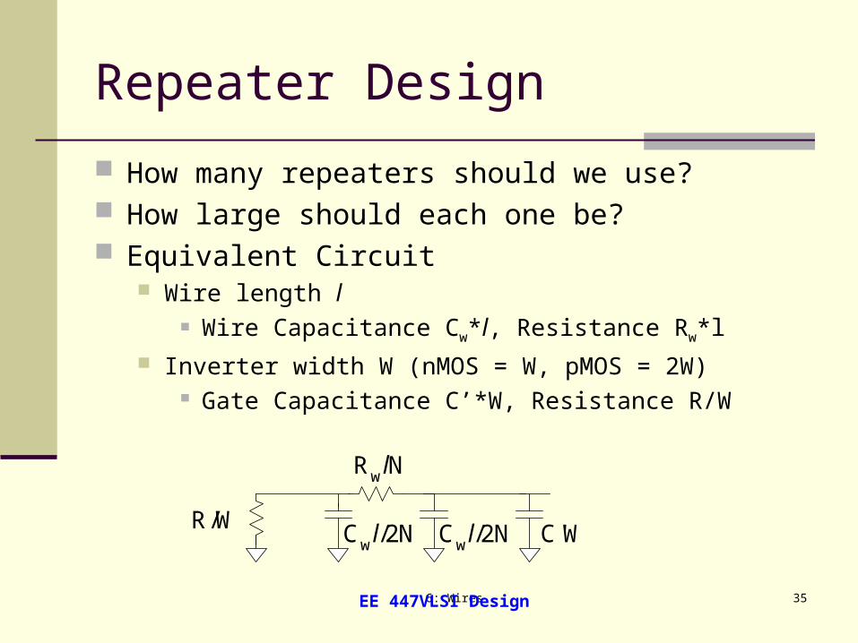
Repeater Design
How many repeaters should we use? How large should each one be? Equivalent Circuit
Wire length l Wire Capacitance Cw*l, Resistance Rw*l
Inverter width W (nMOS = W, pMOS = 2W) Gate Capacitance C’*W, Resistance R/W
R/WC'WCwl/2N Cwl/2N
RwlN
6: Wires 36EE 447VLSI Design
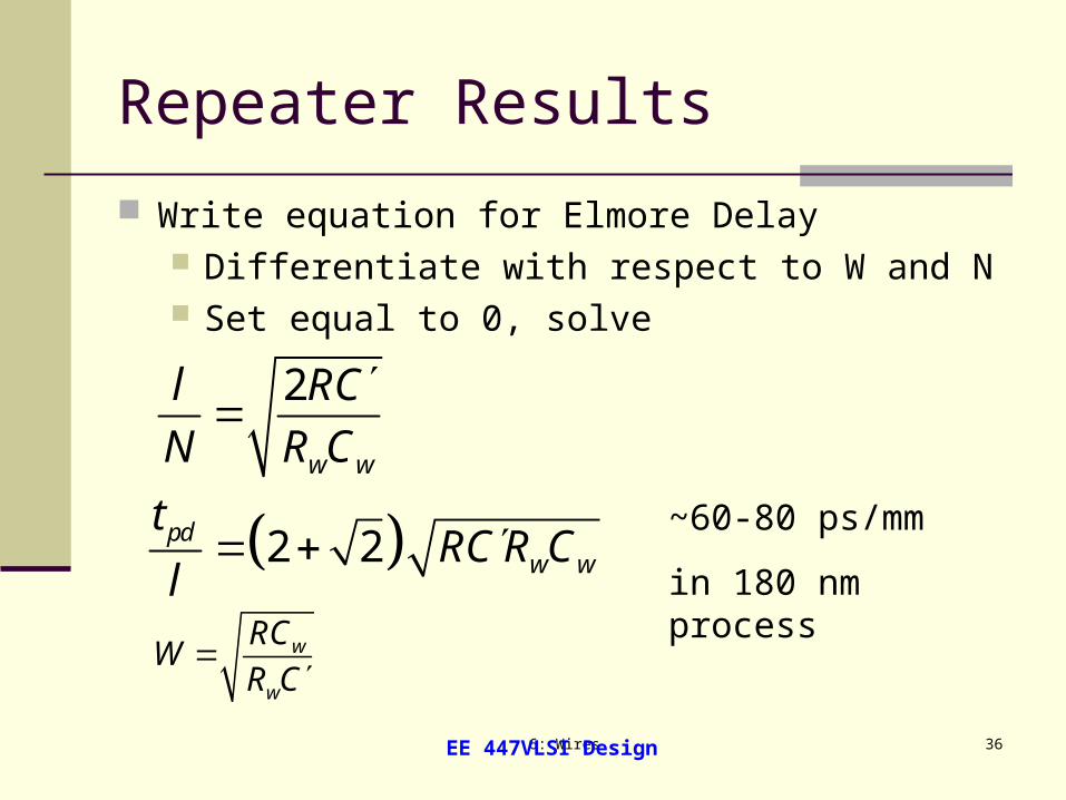
Repeater Results
Write equation for Elmore Delay Differentiate with respect to W and N Set equal to 0, solve
2
w w
l RC
N R C
2 2pdw w
tRC R C
l
w
w
RCW
R C
~60-80 ps/mm
in 180 nm process