EE 361 Fall 2003University of Hawaii1 Hardware Design Tips EE 361 University of Hawaii.
61
EE 361 Fall 2003 University of Hawaii 1 Hardware Design Tips EE 361 University of Hawaii
-
Upload
rudy-tidmore -
Category
Documents
-
view
223 -
download
4
Transcript of EE 361 Fall 2003University of Hawaii1 Hardware Design Tips EE 361 University of Hawaii.

EE 361 Fall 2003 University of Hawaii 1
Hardware Design Tips
EE 361
University of Hawaii

EE 361 Fall 2003 University of Hawaii 2
Outline
• Verilog: some subleties
• Simulators
• Test Benching
• Implementing the MIPS– Actually a simplified 16 bit version

EE 361 Fall 2003 University of Hawaii 3
Monday
• Overview of verilog, again
• Implementing combinational circuits using verilog– Rules to avoid problems

EE 361 Fall 2003 University of Hawaii 4
Verilog
• Basic module
• Combinational subcircuits
• Sequential subcircuits (on wed)

EE 361 Fall 2003 University of Hawaii 5
Verilog: Basic Modulemodule circuitName(y1,y2,clock,reset,select,x1,x2,x3)
output y1,y2;input clock, reset;input select, x1, x2, x3;
wire h1,h2,h3;reg k1,k2;
// InstantiationsCircuit circuit1(h1,h2,clock,h3,5,k1,k2);
endmodule
outputs: only wire variables
inputs: wire vars, reg variables, constants

EE 361 Fall 2003 University of Hawaii 6
Combinational Circuits
• Continuous assign
• Procedural always– Rules– Examples of errors– More rules

EE 361 Fall 2003 University of Hawaii 7
Verilog: Combinational Subcircuits
Continuous assign
wire var
Formula ( no begin-end blocks, if-else, case statements, or anything else)
assign y = x1 + x2 + 3;
Combinationalsubcircuit
x1x2x3
y

EE 361 Fall 2003 University of Hawaii 8
Verilog: Combinational Subcircuits
Procedural always
always @(x1 or x2 or … or xk)
A description of how to computeoutputs from the inputs
Example:always @(x1 or x2) y = x1 + x2 + 3;
From this descriptionyou should be able towrite a truth table forthe circuit
Be sure the table is complete, i.e., it covers all possible inputs ORFor all input values, there should be an output value
Sensitivity ListRule of thumb:List of all inputs

EE 361 Fall 2003 University of Hawaii 9
Example: missing an input inthe sensitivity list
// 2:1 multiplexer module mux(y, sel, a, b)input a, b, sel;output y;always (a or b or sel) begin if (sel == 0) y = a; else y = b; endendmodule
// 2:1 multiplexer module mux(y, sel, a, b)input a, b, sel;output y;always (a or b) begin if (sel == 0) y = a; else y = b; endendmodule
Case of missing aninput (“sel”) in the sensitivity list.

EE 361 Fall 2003 University of Hawaii 10
Example: outputs are not defined for all inputs
// 2:1 multiplexer module mux(y, sel, a, b)input a, b, sel;output y;always (a or b or sel) begin if (sel == 0) y = a; else y = b; endendmodule
// 2:1 multiplexer module mux(y, sel, a, b)input a, b, sel;output y;always (a or b or sel) begin if (sel == 0) y = a; endendmodule
Case of not updating y for all inputs
ay
sel
Possible hardwareimplementation
It’s a transparentD latch
2:1 mux

EE 361 Fall 2003 University of Hawaii 11
Examplealways @(x1 or x2 or s) begin if (s == 1) h = 0; else h = 1; case(h) 0: y = x1|x2; // AND the inputs 1: y = x1&x2; // OR the inputs endcase end
Computation proceedsdownwards(just like C language)
Input Output s x1 x2 y 0 0 0 0 0 0 1 1 0 1 0 1 0 1 1 1 1 0 0 0 1 0 1 0 1 1 0 0 1 1 1 1
Truth tablefor circuit
Next, we’ll present some rules touse procedural always to modelcombinational circuits
Variablesinputs: x1, x2, soutput: yintermediate value: h

EE 361 Fall 2003 University of Hawaii 12
Rules for procedural-always to model combinational circuits
Assignments
y = x1 + x2 + 3;
Blocking assignment (we’ll discuss blocking and nonblocking assignments shortly)
reg variable
Note that the left hand side is always an output orintermediate variable

EE 361 Fall 2003 University of Hawaii 13
Rules for procedural-always to model combinational circuits
Update variables at most once
always @(x1 or x2) begin y = x1 + x2; if (y > 4) y = x1; else y = x2; end
y could be updated morethan once BUT outputs shouldn’t change twice when inputs change
always @(x1 or x2) begin r = x1 + x2; if (r > 4) y = x1; else y = x2; end
We introduced a new regvariable r.
Now “r” and “y” are updatedat most once.

EE 361 Fall 2003 University of Hawaii 14
Rules for procedural-always to model combinational circuits
always @(x1 or x2) begin
end
blocking assigments (e.g., y = x1+x2;)if-elsecase statements
module ....
always @(x1 or x2) begin Circuit circ1(y,x1,x2); end
endmodule
module Circuit(h,g1,g2)output h;input g1, g2
assign h=g1+g2;endmodule
This won’t work.A module is nota C function.

EE 361 Fall 2003 University of Hawaii 15
Some rules to design combinational circuits with “always”
• Sensitivity list should have all inputs• Outputs should have values for all possible inputs• Variables that are updated (left side of blocking
assignments) should be a register variable• Update each variable at most once per change in
input.• Module instantiations are not C function calls
– Use blocking assignments, case, if-else, maybe others such as “for” but be careful.

EE 361 Fall 2003 University of Hawaii 16
Wednesday
• Sequential circuits with verilog
• Electronic Design Automation (EDA)

EE 361 Fall 2003 University of Hawaii 17
Sequential Circuits
• Procedural always
• Examples
• Nonblocking and blocking assignments

EE 361 Fall 2003 University of Hawaii 18
Rules for procedural-always to model sequential circuits
x1x2x3
clock
y1y2
always @(posedge clock)
state = state
Update the state
we’ll assume this
Example: D flip flop
always @(posedge clock) q <= d;
Example: T flip flop
always @(posedge clock) if (t == 1) q <= ~q;
nonblocking assignments
state vars arereg vars.

EE 361 Fall 2003 University of Hawaii 19
Nonblocking AssignmentsD Q
clock
A
D Q
clock
B
D Q
clock
C
clock
0 All flip flops get updatedtogether on a positiveclock edge.
always @(posedge clock) begin A <= 0; B <= A; C <= B; end
All nonblocking assignments areupdated together on the positiveedge of the clock.
D Q
clock
A
D Q
clock
B
D Q
clock
C
clock
01 0 1
Before clock edge
D Q
clock
A
D Q
clock
B
D Q
clock
C
clock
00 1 0
After clock edge
Example

EE 361 Fall 2003 University of Hawaii 20
Nonblocking AssignmentsD Q
clock
A
D Q
clock
B
D Q
clock
C
clock
0
beginA <= 0;B <= A;C <= B;end
beginA = 0;B = A;C = B;end
Suppose initially (A,B,C) = (1,1,1)
(A,B,C) = (0,1,1) (A,B,C) = (0,0,0)

EE 361 Fall 2003 University of Hawaii 21
Example: 2-bit countermodule counter2(q,clock,s,d)out [1:0] q; // 2-bit outputin clock;s [1:0] s; // Select inputin [1:0] d; // Parallel load input reg [1:0] q; // This is our state variable always @(posedge clock) begin case (s) 0: q<=0; 1: q<=q+1; // Counting up. Note that the count wraps around // when it goes past the value 3 2: q<=q-1; // Counting down. Also has wrap around 3: q<=d; // Parallel load endcase // Actually, the begin-end is unnecessary endendmodule
d[1]d[0]
q[1]q[0]
s[1] s[0] clock
s = 0: reset q = 0s = 1: count up s = 2: count downs = 3: load

EE 361 Fall 2003 University of Hawaii 22
Example: Lightsmodule Lights(y,clock,s,d)out [3:0] y; // 4-bit outputin clock;s [1:0] s; // Select inputin [1:0] d; // Parallel load input reg [1:0] q; // This is our state variable always @(posedge clock) begin case (s) 0: q<=0; 1: q<=q+1; // Counting up. Note that the count wraps around // when it goes past the value 3 2: q<=q-1; // Counting down. Also has wrap around 3: q<=q; // Hold endcase // Actually, the begin-end is unnecessary end// Continued
y[3] y[2] y[1] y[0]
s[1] s[0]
clock
s = 0: reset y=1000s = 1: rotate right s = 2: rotate lefts = 3: hold

EE 361 Fall 2003 University of Hawaii 23
Example: Lights// Continued always @(q) case (q) 0: y=4’b1000; 1: y=4’b0100; 2: y=4’b0010; 3: y=4’b0001; endcase endmodule
y[3] y[2] y[1] y[0]
s[1] s[0]
clock
s = 0: reset y=1000s = 1: rotate right s = 2: rotate lefts = 3: hold

EE 361 Fall 2003 University of Hawaii 24
Electronic Design Automation
• Simulator
• EDA process
• Test bench

EE 361 Fall 2003 University of Hawaii 25
Simulators, e.g., veriwell and Modelsim
Simulator will simulate what a circuit will do over time.
Time is divided into time units (fictitious) but you can think of them as some small time duration, e.g., 0.1ns
A variable keeps track of the “current time” (e.g., $time) Initially, “current time” = 0 (or 1)
Update variable values at time 1 based upon values at time 0
Update variable values at time 2 based upon values at time 1
and so on.

EE 361 Fall 2003 University of Hawaii 26
Example0
0 1
$time = 00
0 1
new value based on
1
0
1 1
$time = 1
0
1 0
$time = 2

EE 361 Fall 2003 University of Hawaii 27
Simulatorverilogcircuit module
synthesizer
hardware
verilogtestbench
module
project
simulator
verify thatyour circuit
works(debugging)

EE 361 Fall 2003 University of Hawaii 28
Test BenchProtoboard
5V Gnd
Clock Generator
IC Chip
LEDs(probes)
inputs to excitethe circuit
outputs to observebehavior

EE 361 Fall 2003 University of Hawaii 29
module testbench;
reg clock; // Clock signalreg [1:0] A; // Inputs A and B to excitereg [2:0] B;wire [2:0] C; // Output C to observe
icChip c1(A,B,C,clock); // Instantiation of the circuit to test
init clock = 0; // Clock generation, with clock period = 2 time unitsalways #1 clock = ~clock;
init // Changing inputs to excite icChip c1begin: Input values for testingA = 0;B = 0;#2 A = 1; // After 2 time units, A is changed to 1.#1B = 3; // After another time unit, B changes to 3.#2 $stop; // After 2 more time units, the simulation stopsend
init // Display of outputsbegin: Display$display("A B C clock time"); // Displayed once at $time = 0$monitor("%d %d %d %d %d",A,B,C,clock,$time); // Displayed whenever variable changes// Note that $monitor can occur at most once in verilog code// while $display can occur many times.end
endmodule

EE 361 Fall 2003 University of Hawaii 30
Friday
• Building single cycle MIPS – naive way
• MIPS-L: 16 bit version of MIPS
• Build it in stages– MIPS-L0: executes only R-type
instructions• Tips on testing and debugging
– MIPS-L1, L2, L3

EE 361 Fall 2003 University of Hawaii 31
Building Single Cycle MIPSHow NOT to build a single cycle MIPS in verilog.
1. Build all the components in verilog. 2. Test/debug each component3. Put everything together into the single cycle MIPS4. Simulate --> syntax errors5. Fix syntax errors, and then simulate --> ‘xxx’6. Hmmm. Maybe I’m unlucky. Simulate again.7. Hmmm. Must be the simulator. Reset PC. Simulate again.8. Problem too hard -- it’s a complicated computer after all
First three steps are okay. But need improvement after that.

EE 361 Fall 2003 University of Hawaii 32
MIPS-L
• To experience building a moderately large circuit, you will build a MIPS computer– Homework 10A and 10B
• MIPS-L: 16 bit version of MIPS– Description– Simplified version MIPS-L0
• Only R-type arithmetic instructions• Modified register file: RegFileL0
EE 361 Fall 2003 University of Hawaii 33
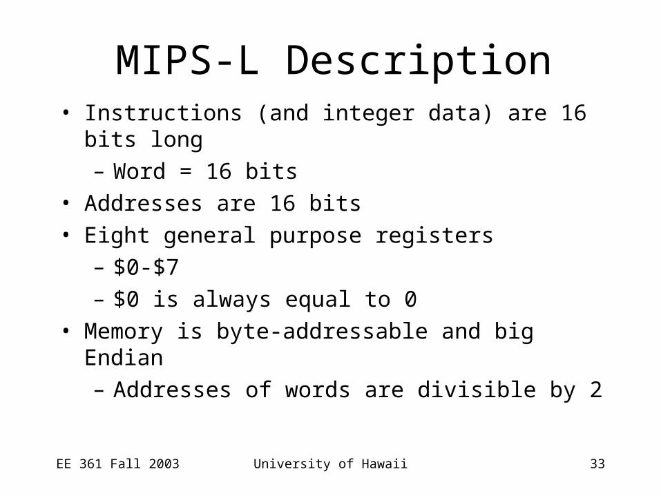
MIPS-L Description• Instructions (and integer data) are 16 bits long
– Word = 16 bits• Addresses are 16 bits• Eight general purpose registers
– $0-$7– $0 is always equal to 0
• Memory is byte-addressable and big Endian– Addresses of words are divisible by 2

EE 361 Fall 2003 University of Hawaii 34
MIPS-L Register Convention
Name Register
Number
Usage Preserved on call?
$zero 0 the constant 0 n.a.
$v0-$v1 1-2 values for results and expression evaluation
No
$t0-$t2 3-5 temporaries No
$sp 6 stack pointer Yes
$ra 7 return address No

EE 361 Fall 2003 University of Hawaii 35
MIPS-L Instruction Formats
Name Fields Comments
Field
Size
3 bits 3 bits 3 bits 3 bits 4 bits ALL MIPS-L instructions 16 bits
R-
format
op rs rt rd funct Arithmetic instruction format
I-
format
op rs rt rd Address/
immediate
Transfer, branch, immediate format
J-
format
op target address Jump instruction format

EE 361 Fall 2003 University of Hawaii 36
MIPS-L Machine InstructionsName Format Example Comments
3 bits 3 bits 3 bits 3 bits 4 bits
add R 0 2 3 1 0 add $1,$2,$3
sub R 0 2 3 1 1 sub $1,$2,$3
and R 0 2 3 1 2 and $1,$2,$3
or R 0 2 3 1 3 or $1,$2,$3
slt R 0 2 3 1 4 slt $1,$2,$3
jr R 0 7 0 0 8 jr $7
lw I 4 2 1 100 lw $1,100($2)
sw I 5 2 1 100 sw $1,100($2)
beq I 6 1 2 (offset to 100)/2 beq $1,$1,100
addi I 7 2 1 100 addi $1,$2,100
j J 2 5000 j 10000
jal J 3 5000 jal 10000

EE 361 Fall 2003 University of Hawaii 37
Shiftleft 2
PC
Instructionmemory
Readaddress
Instruction[31– 0]
Datamemory
Readdata
Writedata
RegistersWriteregister
Writedata
Readdata 1
Readdata 2
Readregister 1
Readregister 2
Instruction [15– 11]
Instruction [20– 16]
Instruction [25– 21]
Add
ALUresult
Zero
Instruction [5– 0]
MemtoReg
ALUOp
MemWrite
RegWrite
MemRead
Branch
JumpRegDst
ALUSrc
Instruction [31– 26]
4
Mux
Instruction [25– 0] Jump address [31– 0]
PC+4 [31– 28]
Signextend
16 32Instruction [15– 0]
1
Mux
1
0
Mux
0
1
Mux
0
1
ALUcontrol
Control
Add ALUresult
Mux
0
1 0
ALU
Shiftleft 2
26 28
Address
Single Cycle MIPS-L
This thing’s got a cycle in it. Not good. Build it in stages The following is JUST A SUGGESTION

EE 361 Fall 2003 University of Hawaii 38
MIPS-L0
• Something even simpler: MIPS-L0
• Only executes R format arithmetic instructions
• Register File RegFileL0– Register $5 = 1 always– Register $4 = 2 always
• ALUControl: Same as MIPS-L

EE 361 Fall 2003 University of Hawaii 39
MIPS-L0
MIPS-L0
clock
InstructionMemory(ROM)
iaddr
idata
reset
aluout
aluina
aluinb
Used to verify correctness
Everything is 16 bits except reset and clock

EE 361 Fall 2003 University of Hawaii 40
MIPS-L0• Describe MIPS-L0
• Example Program Memory– Example testbench– General testbench of simple combination circuits
• Building Single Cycle MIPS-L0– Pre MIPS-L0, yet even simpler– Debugging tips
• Building Single Cycle MIPS-L

EE 361 Fall 2003 University of Hawaii 41
MIPS-L0clock
iaddr
idata(instruction)
reset
aluout
aluina
aluinb
PC
+
4
RegFileL0
r2
r3
r1
ALU
RegWrite=1
ALUControl
ALUOp=2

EE 361 Fall 2003 University of Hawaii 42
Example Instruction Memory// Instruction memory// Program has only 8 instructionsmodule IM(addr, dout)input [15:0] addr;dout [15:0] dout;reg [15:0] dout;
always @(addr[3:1]) case (addr[3:1])
0: dout = {3’d0,3’d4,3’d5,3’d3,4’d0} // add $3,$4,$51: dout = // sub $2,$4,$52: dout = // slt $1,$4,$53: dout = // and $1,$3,$54: dout = // slt $1,$4,$35: dout = // sub $1,$3,$56: dout = // add $3,$0,$27: dout = // add $3,$5,$1
endcaseendmodule

EE 361 Fall 2003 University of Hawaii 43
Example Testbench// Testbench for program memorymodule testbench_memoryreg [15:0] addr;wire [15:0] dout;
IM pmem(addr, dout); // Instantiation of memory
initial begin // Drive the memory addr = 0; #2 addr = 2; #2 addr = 4;...... #2 addr = 14; #2 $stop;end
initial begin // Display the outputs$monitor(“time = %d, addr=%d, instr=(%d,%d,%d,%d,%d)”,$time,addr,dout[15:13],...endendmodule

EE 361 Fall 2003 University of Hawaii 44
Simple Testbenches• Declare reg variables to drive inputs• Declare wire variables to tap into outputs
and connect circuits• Clock generator signal (if necessary)• Set up circuit with instantiations and
possible connections• Initial procedure to change input signals
over time (use delays # and $stop)• Initial procedure to output results

EE 361 Fall 2003 University of Hawaii 45
Building MIPS-L0
• Build the components and test– Instruction memory– ALU– ALU Control– Register file RegFileL0
• Build and test a Pre-MIPS-L0 (see next slide)
• Build and test a MIPS-L0 (finally!)

EE 361 Fall 2003 University of Hawaii 46
Pre MIPS-L0
We got rid of the cycle
clock
iaddr
idata(instruction)
reset
aluout
aluina
aluinb
PC
+
4
RegFileL0
r2
r3
r1
ALU
RegWrite=1
ALUControl
ALUOp=2
9 is an arbitrary number
9

EE 361 Fall 2003 University of Hawaii 47
Pre MIPS-L0
• What do we gain by removing the cycle?– If there’s a bug, we can find it by tracing
backwards
• Testbench– Has an instantiation of MIPS-LO and
program memory– Try different programs for testing

EE 361 Fall 2003 University of Hawaii 48
Pre MIPS-L0
• Rules of thumb for debugging– Determine a set of input signals to test
whether the circuit works or not– Input signals will vary over time– Determine where to probe signals
• At outputs• At intermediate points
– Determine by hand what signals to expect

EE 361 Fall 2003 University of Hawaii 49
Pre MIPS-L0
• Rules of thumb for debugging– Create test bench that
• generates the appropriate input signals over time
• outputs the signals you want
– Run the test bench and see if the circuit works
– If not, put probe signals upstream to determine where the problem is

EE 361 Fall 2003 University of Hawaii 50
Probing Upstream
0
probe
This is supposedto be “1”.
Check upstream until you find a device that isn’t working,
e.g., outputs don’t match inputs

EE 361 Fall 2003 University of Hawaii 51
Pre MIPS-L0
• Rules of thumb for debugging– Change input signals to REALLY verify that
the circuit will work under all conditions• Example: change program

EE 361 Fall 2003 University of Hawaii 52
MIPS-L0
• After verifying correctness of Pre MIPS-LO, build and test MIPS-L0
• This is Homework 10A

EE 361 Fall 2003 University of Hawaii 53
MIPS-L
• Build the MIPS-L in stages• Stage 1 MIPS-L1
– Include addi and j– Use ordinary register file– Include Control circuit
• Stage 2 MIPS-L2: – include beq– Modify ALU for zero output

EE 361 Fall 2003 University of Hawaii 54
MIPS-L
• Stage 3 MIPS-L3 (final)– Include lw and sw– Have the RAM store 128 words.– RAM is implemented like a register file
• Have the program read and write to RAM and check if it does so properly
• Verification can be done by checking inputs and outputs
– This is Homework 10B

EE 361 Fall 2003 University of Hawaii 55
Testbenching
• Your testbench should include– Your MIPS-Lx– Program memory
• Don’t be afraid to try different programs for testing
• Last slide unless there’s more time

EE 361 Fall 2003 University of Hawaii 56
Shiftleft 2
PC
Instructionmemory
Readaddress
Instruction[31– 0]
Datamemory
Readdata
Writedata
RegistersWriteregister
Writedata
Readdata 1
Readdata 2
Readregister 1
Readregister 2
Instruction [15– 11]
Instruction [20– 16]
Instruction [25– 21]
Add
ALUresult
Zero
Instruction [5– 0]
MemtoReg
ALUOp
MemWrite
RegWrite
MemRead
Branch
JumpRegDst
ALUSrc
Instruction [31– 26]
4
Mux
Instruction [25– 0] Jump address [31– 0]
PC+4 [31– 28]
Signextend
16 32Instruction [15– 0]
1
Mux
1
0
Mux
0
1
Mux
0
1
ALUcontrol
Control
Add ALUresult
Mux
0
1 0
ALU
Shiftleft 2
26 28
Address
Single Cycle MIPS
set these multiplexersso that PC=PC+4
Build this first.Your programshould have R-type,lw, sw, and j instructions only

EE 361 Fall 2003 University of Hawaii 57
Shiftleft 2
PC
Instructionmemory
Readaddress
Instruction[31– 0]
Datamemory
Readdata
Writedata
RegistersWriteregister
Writedata
Readdata 1
Readdata 2
Readregister 1
Readregister 2
Instruction [15– 11]
Instruction [20– 16]
Instruction [25– 21]
Add
ALUresult
Zero
Instruction [5– 0]
MemtoReg
ALUOp
MemWrite
RegWrite
MemRead
Branch
JumpRegDst
ALUSrc
Instruction [31– 26]
4
Mux
Instruction [25– 0] Jump address [31– 0]
PC+4 [31– 28]
Signextend
16 32Instruction [15– 0]
1
Mux
1
0
Mux
0
1
Mux
0
1
ALUcontrol
Control
Add ALUresult
Mux
0
1 0
ALU
Shiftleft 2
26 28
Address
Single Cycle MIPS
set these multiplexersso that PC=PC+4
Check controlleroutputs

EE 361 Fall 2003 University of Hawaii 58
Shiftleft 2
PC
Instructionmemory
Readaddress
Instruction[31– 0]
Datamemory
Readdata
Writedata
RegistersWriteregister
Writedata
Readdata 1
Readdata 2
Readregister 1
Readregister 2
Instruction [15– 11]
Instruction [20– 16]
Instruction [25– 21]
Add
ALUresult
Zero
Instruction [5– 0]
MemtoReg
ALUOp
MemWrite
RegWrite
MemRead
Branch
JumpRegDst
ALUSrc
Instruction [31– 26]
4
Mux
Instruction [25– 0] Jump address [31– 0]
PC+4 [31– 28]
Signextend
16 32Instruction [15– 0]
1
Mux
1
0
Mux
0
1
Mux
0
1
ALUcontrol
Control
Add ALUresult
Mux
0
1 0
ALU
Shiftleft 2
26 28
Address
Single Cycle MIPS
Check registerfile outputs.You must initialize register values somehow
RegWrite=0 whiletesting at this stage

EE 361 Fall 2003 University of Hawaii 59
Shiftleft 2
PC
Instructionmemory
Readaddress
Instruction[31– 0]
Datamemory
Readdata
Writedata
RegistersWriteregister
Writedata
Readdata 1
Readdata 2
Readregister 1
Readregister 2
Instruction [15– 11]
Instruction [20– 16]
Instruction [25– 21]
Add
ALUresult
Zero
Instruction [5– 0]
MemtoReg
ALUOp
MemWrite
RegWrite
MemRead
Branch
JumpRegDst
ALUSrc
Instruction [31– 26]
4
Mux
Instruction [25– 0] Jump address [31– 0]
PC+4 [31– 28]
Signextend
16 32Instruction [15– 0]
1
Mux
1
0
Mux
0
1
Mux
0
1
ALUcontrol
Control
Add ALUresult
Mux
0
1 0
ALU
Shiftleft 2
26 28
Address
Single Cycle MIPS
Complete datapathbut not writing toanything
RegWrite=0 andMemWrite = 0while testing at this stage

EE 361 Fall 2003 University of Hawaii 60
Shiftleft 2
PC
Instructionmemory
Readaddress
Instruction[31– 0]
Datamemory
Readdata
Writedata
RegistersWriteregister
Writedata
Readdata 1
Readdata 2
Readregister 1
Readregister 2
Instruction [15– 11]
Instruction [20– 16]
Instruction [25– 21]
Add
ALUresult
Zero
Instruction [5– 0]
MemtoReg
ALUOp
MemWrite
RegWrite
MemRead
Branch
JumpRegDst
ALUSrc
Instruction [31– 26]
4
Mux
Instruction [25– 0] Jump address [31– 0]
PC+4 [31– 28]
Signextend
16 32Instruction [15– 0]
1
Mux
1
0
Mux
0
1
Mux
0
1
ALUcontrol
Control
Add ALUresult
Mux
0
1 0
ALU
Shiftleft 2
26 28
Address
Single Cycle MIPS
Program justhas R-type andj instructions
MemWrite = 0while testing at this stage

EE 361 Fall 2003 University of Hawaii 61
Shiftleft 2
PC
Instructionmemory
Readaddress
Instruction[31– 0]
Datamemory
Readdata
Writedata
RegistersWriteregister
Writedata
Readdata 1
Readdata 2
Readregister 1
Readregister 2
Instruction [15– 11]
Instruction [20– 16]
Instruction [25– 21]
Add
ALUresult
Zero
Instruction [5– 0]
MemtoReg
ALUOp
MemWrite
RegWrite
MemRead
Branch
JumpRegDst
ALUSrc
Instruction [31– 26]
4
Mux
Instruction [25– 0] Jump address [31– 0]
PC+4 [31– 28]
Signextend
16 32Instruction [15– 0]
1
Mux
1
0
Mux
0
1
Mux
0
1
ALUcontrol
Control
Add ALUresult
Mux
0
1 0
ALU
Shiftleft 2
26 28
Address
Single Cycle MIPS