EE 140/240A Linear Integrated Circuits Homework...
22
Last Updated: 2019-10-31 10:50 1 EE 140/240A Linear Integrated Circuits Fall 2019 Homework 8 1. (Spring 2015 Midterm 2 Q4) The TI OPA334 is a single-ended CMOS op-amp similar to what you’ve been designing in class. The frequency response from the datasheet is shown below. (a) What is the open loop gain? Solution: This is approximately half a decade above 10 6 , so 3 × 10 6 V/V Rubric: (2 Points) • +2: Correct open loop gain (acceptable to estimate as half on the log scale or linear scale) (b) What is the lowest frequency pole? Solution: f 3dB ≈ 0.8Hz Rubric: (2 Points) • +2: Correct pole frequency UCB EE 140/240A, Fall 2019, Homework 8 1
Transcript of EE 140/240A Linear Integrated Circuits Homework...

Last Updated: 2019-10-31 10:50 1
EE 140/240A Linear Integrated CircuitsFall 2019 Homework 8
1. (Spring 2015 Midterm 2 Q4)
The TI OPA334 is a single-ended CMOS op-amp similar to what you’ve been designing in class. Thefrequency response from the datasheet is shown below.
(a) What is the open loop gain?Solution:
This is approximately half a decade above 106, so 3×10⁶V/V
Rubric: (2 Points)
• +2: Correct open loop gain (acceptable to estimate as half on the log scale or linear scale)
(b) What is the lowest frequency pole?Solution:
f3dB ≈ 0.8Hz
Rubric: (2 Points)
• +2: Correct pole frequency
UCB EE 140/240A, Fall 2019, Homework 8 1

Last Updated: 2019-10-31 10:50 2
(c) What is the phase margin?Solution:
φPM ≈ 80°
Rubric: (2 Points)
• +2: Correct phase margin
(d) Is the amplifier unity-gain stable?Solution:
Yes
Rubric: (2 Points)
• +2: Correct answer
2. (Spring 2015 Midterm 2 Q6)
In the two-stage op-amp below, assuming Iref = 10µA and (W/L)6 = 10µm/1µm, design the amplifier sothat the tail current is 20µA, the second stage current is 100µA, and the PMOS devices have Vov = 100mV.
Process specs:
• µnCox = 2µpCox = 200µA/V2
• λ = 1/(10V)
• Vtn =−Vt p = 0.5V• VDD = 2V
• Lmin = 1µm
• Cox = 5fF/µm2
• C′ol = 0F/µm
1A 1B
2A 2B
3
4
56
Iref
Rz
CCV− V+ Vout
VDD
C2
UCB EE 140/240A, Fall 2019, Homework 8 2

Last Updated: 2019-10-31 10:50 3
(W/L)1
(W/L)2
(W/L)3
(W/L)4
(W/L)5
(W/L)6 10µm/1µm
gm1
Ro1
gm4
Ro2
Av1
Av2
Solution: Our spec is quite straightforward, but the point of this question was more so making surestudents knew how to find the important small signal parameters of an amplifier they designed. Here goes!
(a) Tail current is 20µA: Given that Iref = 10µA, we know that M3 = 2M6 −→ (W/L)3 = 20µm/1µm
(b) Second stage current is 100µA: Similar to what we did for M3, we’ll do for M5, so M5 = 10M6−→ (W/L)5 = 100µm/1µm
(c) PMOS devices have Vov = 100mV: This means VG2 and VG4 are equal (which makes sense for matchingwith the current mirror load) and are at a particular voltage VDD−|Vtn|−Vov −→VG2 =VG4 = 1.4V
(d) Now calculating the size of the PMOS devices to sink the appropriate amount of current given ouroverdrive
WL
=2ID
µpCoxV 2ov
−→ (W/L)2 = 20µm/1µm,(W/L)4 = 200µm/1µm
(e) At this point, we’re almost finished! It just becomes a question of what overdrive voltage we want todrive our input pair at. For the sake of this problem, we can go with something fairly small like 100mVto size our input devices −→ (W/L)1 = 10µm/1µm
Our equations of interest after all of that are as follows:
gm =2ID
Vov
ro =1
λ ID
Ro1 ≈ ro2B||ro1B
Ro2 ≈ ro4||ro5
(W/L)1 10µm/1µm(W/L)2 20µm/1µm(W/L)3 20µm/1µm(W/L)4 200µm/1µm(W/L)5 100µm/1µm(W/L)6 10µm/1µm
gm1 0.2µSRo1 500kΩ
gm4 2µSRo2 50kΩ
Av1 −100Av2 −100
Rubric: (28 Points)
• +1: Correct approach for finding W/L of device (×7)
• +1: Correct numerical value for W/L of device (×7)
UCB EE 140/240A, Fall 2019, Homework 8 3

Last Updated: 2019-10-31 10:50 4
• +1: Correct approach for each of gm, Ro, and Av calculation (×6)
• +1: Correct numerical value for each of gm, Ro, and Av (×6)
• +2: Some indication that ID through each M2 and M1 should be 10µA (half the tail current)
3. (Spring 2015 Midterm 2 Q7)
1A 1B
2A 2B
3
4
56
Iref
Rz
CCV− V+ Vout
VDD
C2
A design of the 2-stage op-amp above has the following parameters
gm1 Ro1 gm4 Ro2 C2 CC Cgs4
1µS 100MΩ 10µS 100MΩ 1pF 10fF 100fF
(a) What are the uncompensated (CC = 0) DC gain and pole locations of the two stages?Solution: First the pole locations
ωp1 =1
Ro1C1
≈ 1100 ·106 ·100 ·10−15
=1
102+6+2−15
=1
10−5
= 100krad/s
ωp2 =1
Ro2C2
=1
100 ·106 ·1 ·10−12
=1
102+6−12
=1
10−4
= 10krad/s
And then the gain
Av1 =−gm1Ro1
=−1 ·10−6 ·100 ·106
=−100
Av2 =−gm4Ro2
=−10 ·100
=−1000
UCB EE 140/240A, Fall 2019, Homework 8 4

Last Updated: 2019-10-31 10:50 5
ωp1 = 100krad/s
ωp2 = 10krad/s
Av1 =−100
Av2 =−1000
(b) Now reinsert CC from the table. What is the frequency of the RHP zero? Assume Rz = 0Ω.Solution:
ωz,RHP =gm2
CC
= 1Grad/s
ωz,RHP = 1Grad/s
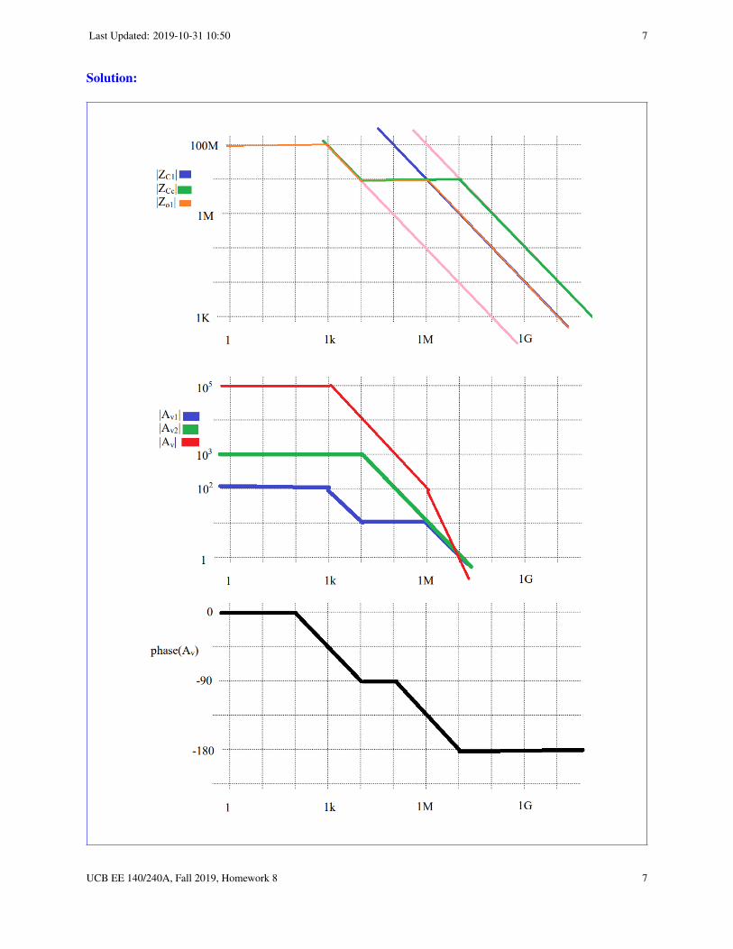
(c) On the next page, on the top axes plot the magnitude of the impedance of C1, CC by itself, and the totalimpedance seen at the first stage output.Rubric: (5 Points)
• +1: Correct |ZC1|• +1: Correct low-frequency |ZCc |• +1: Correct transition points for ZCc
• +1: Correct high-frequency |ZCc |• +1: Correct total |Zo1|
(d) On the middle axes plot the magnitude of the compensated first and second stage gains, and the overallgain. You may assume that the value of Rz has been chosen to place the RHP zero at infinity.Rubric: (3 Points)
• +1: Correct |Av1| given Zo1 from previous part (don’t double-penalize)• +1: Completely correct |Av2|• +1: Correct cumulative gain
(e) On the bottom axes plot the phase of the overall gain.Rubric: (2 Points)
• +1: Correct phase transition about first pole• +1: Correct phase transition about second pole
UCB EE 140/240A, Fall 2019, Homework 8 5

Last Updated: 2019-10-31 10:50 6
UCB EE 140/240A, Fall 2019, Homework 8 6
Last Updated: 2019-10-31 10:50 7
Solution:
UCB EE 140/240A, Fall 2019, Homework 8 7

Last Updated: 2019-10-31 10:50 8
4. (Spring 2017 Midterm 2 Q2)
A single-pole amplifier has a gain of 1,000 and a pole at 1MHz. It is used in feedback with a feedback factorf = 0.01. Calculate the following:
(a) Approximate closed-loop gainSolution:
ACL ≈1f
= 100V/V
ACL ≈ 100V/V
Rubric: (2 Points)
• +1: Correct equation 1f
• +2: Correct numerical value
(b) Percent gain errorSolution:
− 1A f×100% =− 1
1000 ·0.01×100%
=−0.1×100%
=−10%
percent gain error =−10%
Rubric: (2 Points)
• +1: Correct equation − 1A f
• +2: Correct numerical value
(c) Closed-loop pole locationSolution:
fp,CL =GBWACL
= 10MHz
fp,CL = 10MHz
Rubric: (2 Points)
• +1: Correct equation GBWACL
UCB EE 140/240A, Fall 2019, Homework 8 8

Last Updated: 2019-10-31 10:50 9
• +2: Correct numerical value
(d) Time constant of the step responseSolution:
τ =1
ωp,CL
=1
2π fp,CL
=10−7
2πs
τ =10−7
2πs
Rubric: (2 Points)
• +1: Correct equation 1ωp,CL
• +2: Correct numerical value
5. (Spring 2017 Midterm 2 Q3)
A particular diode D1 has a saturation current of 1pA, and at 1mA current at room temperature the diodevoltage has a temperature coefficient of−2mV/K. You are using copies of this diode to make a bandgap ref-erence, with D2 composed of seven copies of D1. You can use the approximation that ln(7)≈ 2. Assumingthat the current in both diodes is maintained at 1mA at room temperature,
Rubric: (6 Points)
• +2 for parts a, b, d, e no partial credit.
• +3 for part c.
• +9 for part f, +3 per line/function
UCB EE 140/240A, Fall 2019, Homework 8 9

Last Updated: 2019-10-31 10:50 10
• +2 for part g.
(a) What is the voltage on D1 at room temperature?Solution: Between 1pA and 1mA there are 9 decades, so
9 decades ·60mV = 0.54V
0.54V
(b) What is the voltage on D2 at room temperature?Solution: The voltage is a factor of ln(7)VT smaller than that across D1, so
0.54V−2 ·26mV≈ 0.49V
0.49V
(c) What is the difference between the two diode voltages at 200K, 300K, and 400K?Solution: The difference scales with VT = kBT
q
@200K : 35mV
@300K : 52mV
@400K : 70mV
(d) What is the temperature coefficient of the voltage on D2?Solution:
−2mVK− 52mV
300K≈−2.17
mVK
≈−2.17mVK
(e) Roughly what is the right value for R1?Solution:
R1 =52mV1mA
= 52Ω
UCB EE 140/240A, Fall 2019, Homework 8 10
Last Updated: 2019-10-31 10:50 11
R1 = 52Ω
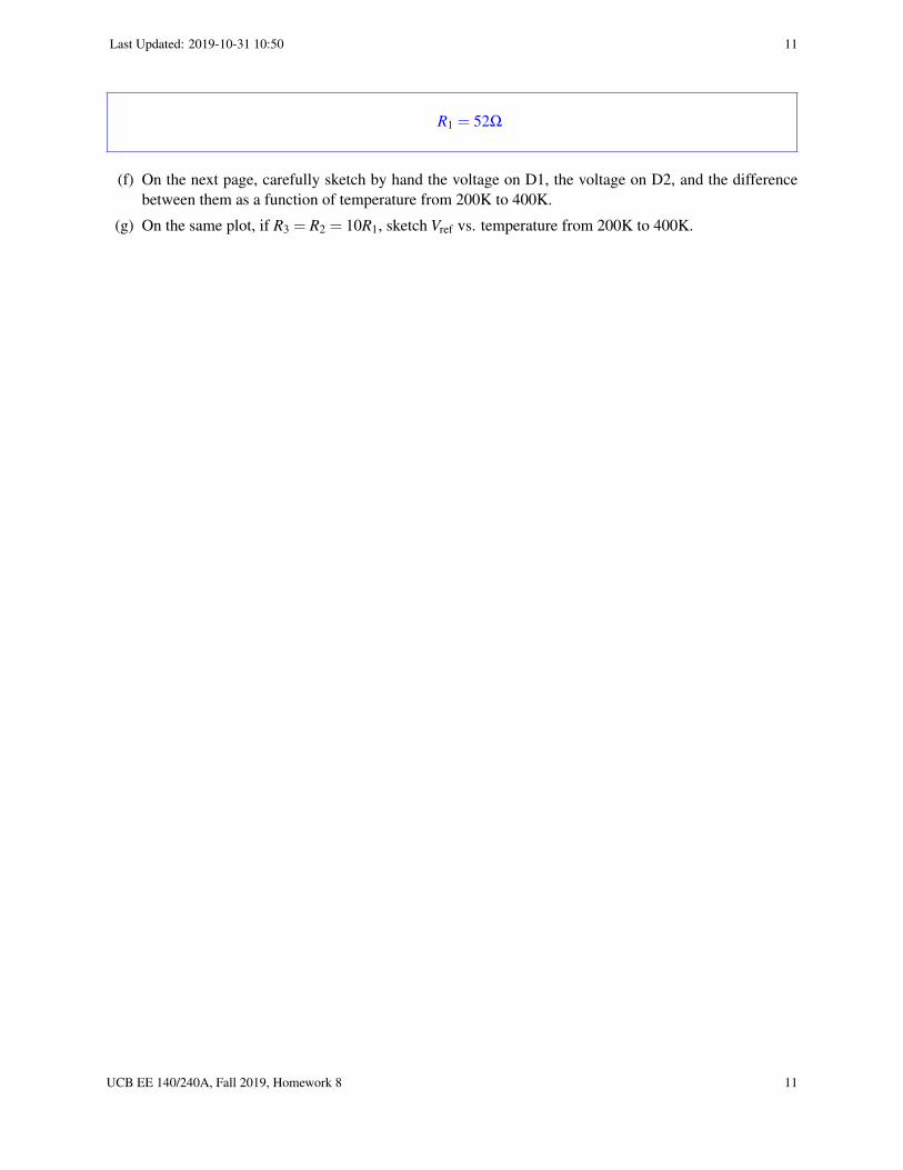
(f) On the next page, carefully sketch by hand the voltage on D1, the voltage on D2, and the differencebetween them as a function of temperature from 200K to 400K.
(g) On the same plot, if R3 = R2 = 10R1, sketch Vref vs. temperature from 200K to 400K.
UCB EE 140/240A, Fall 2019, Homework 8 11

Last Updated: 2019-10-31 10:50 12
UCB EE 140/240A, Fall 2019, Homework 8 12

Last Updated: 2019-10-31 10:50 13
Solution:
6. Surprise, Kids! Bet You Thought You’d Seen the Last of Me!Calculate the common mode gain for the first stage of your op-amp from lab3 part 1.
UCB EE 140/240A, Fall 2019, Homework 8 13

Last Updated: 2019-10-31 10:50 14
Solution:Looking to the half circuit of the first stage, we have
Ro1 ≈1
gm2a
Gm1 ≈1
2ro3
So the common mode gain is approximately
ACM = ACM1A2
≈ 12gm2aro3
×gm4 (ro4||ro5)
Rubric: (4 Points)
• +1: Correct Ro1 for first stage• +1: Correct Gm1 for first stage• +1: Correct voltage gain of second stage• +1: Correct sign of final voltage gain
7. Amps and SlewingFor each of the following four op-amps, redraw the schematic of the op amp including only those transistorsthat are on when the op-amp is slewing positive, and then slewing negative (there should be 8 figures: 2topologies, 2 types of input transistors, 2 slewing directions).
(a) Our standard 5T single stage CMOS op amp with an NMOS input, and with PMOS inputSolution:Devices marked in red are on
1A 1B
2B2A
3VBN
+ −
Vout
(a) Negative slewing
1A 1B
2B2A
3VBN
+ −
Vout
(b) Positive slewing
UCB EE 140/240A, Fall 2019, Homework 8 14

Last Updated: 2019-10-31 10:50 15
1A 1B
2A 2B
3
Vout
VBP
+ −
(a) Negative slewing
1A 1B
2A 2B
3
Vout
VBP
+ −
(b) Positive slewing
Rubric: (12 Points)
• +1: Correct device indicated as on (12×)• -1: Incorrect device indicated as on (minimum 0 points)
(b) The current mirror op-amp with NMOS and with PMOSSolution:Devices marked in red are on
1A 1B
2A 2B
3
4A 4B
5A 5B
Vout− +
VBN
(a) Negative slewing
1A 1B
2A 2B
3
4A 4B
5A 5B
Vout− +
VBN
(b) Positive slewing
UCB EE 140/240A, Fall 2019, Homework 8 15

Last Updated: 2019-10-31 10:50 16
1A 1B
2A 2B
3
4A 4B
5A 5B
Vout− +
VBN
(a) Negative slewing
1A 1B
2A 2B
3
4A 4B
5A 5B
Vout− +
VBN
(b) Positive slewing
Rubric: (20 Points)
• +1: Correct device indicated as on (20×)• -1: Incorrect device indicated as on (minimum 0 points)
8. Two-Stages Slewing
For a two-stage NMOS-input CMOS op-amp with the output stage biased at 10µA and the tail current at1µA
(a) Calculate the positive and negative slew rate if Cc = 1pF and CL = 1pFSolution:
I =CdVdt
dVdt
=IC
In each case we need to consider the possible causes of slewing. For negative slew rate, we considertwo cases and assume Av2 1:
− Itail
Cc=−1µA
1pF
=−1×10⁶ Vs
− ID5
CL=−10µA
1pF
=−10×106 Vs
We choose the most restrictive of the two (the lecture notes say the minimum of two negative values,but it should be the minimum of the absolute value of the two negative values).For positive slew rate, the PMOS of the second stage can nominally provide infinite current so long asits gate is driven correctly, so the first stage + compensation capacitor limit the positive slew rate (the
UCB EE 140/240A, Fall 2019, Homework 8 16

Last Updated: 2019-10-31 10:50 17
compensation cap is Millerized, which removes the gain term that would come from the second stage)
Itail
Cc=
1µA1pF
= 1×10⁶ Vs
positive rate = 1×10⁶ Vs
negative rate = −1×10⁶ Vs
Rubric: (4 Points)
• +1: Correct positive slew rate equation• +1: Correct positive slew rate numerical value• +1: Correct negative slew rate equation• +1: Correct negative slew rate numerical value
(b) Calculate the positive and negative slew rate if Cc = 1pF and CL = 100pFSolution: In a similar fashion as before:
− Itail
Cc=−1µA
1pF
=−1×10⁶ Vs
− ID5
CL=− 10µA
100pF
=−0.1×10⁶ Vs
Itail
Cc=
1µA1pF
= 1×10⁶ Vs
positive rate = 1×10⁶ Vs
negative rate = 0.1×10⁶ Vs
Rubric: (4 Points)
• +1: Correct positive slew rate equation• +1: Correct positive slew rate numerical value• +1: Correct negative slew rate equation• +1: Correct negative slew rate numerical value
9. Getting Funky
In the circuit below
UCB EE 140/240A, Fall 2019, Homework 8 17

Last Updated: 2019-10-31 10:50 18
Solution:Errata: The original amplifier had a PMOS instead of an NMOS for M11! If you noticed that it was aPMOS and stated that it was in positive feedback (and would likely have its output blow up and oscillate),give yourself full credit. If you didn’t notice it was in positive feedback, see the rubrics below in red.
(a) What do we call the amplifier configuration of transistors M10 and M11?Solution:
Source follower (the input is Vout and the output is the RHS of the compensation capacitor)
Rubric: (1 Points)
• +1: Identified as source follower• +1: Common source
(b) Does this additional amplifier prevent or enable Cc from being useful as a Miller compensation capac-itor?Solution:
It enables (or rather, doesn’t block) the first stage from seeing the Millerized Cc
Rubric: (1 Points)
• +1: Correctly stated that it allowed Millerization of the compensation capacitor• +1: Stated that this would actually enhance the Millerization with the gain of the additional com-
mon source stage
UCB EE 140/240A, Fall 2019, Homework 8 18

Last Updated: 2019-10-31 10:50 19
(c) What affect does this additional amplifier have on the right-half plane zero normally present withMiller compensation? Why?Solution:
The output stage no longer sees the feed-forward current, and so the right-half plane zero isremoved! For Fall 2019, see W7L4 notes.
Rubric: (1 Points)
• +1: Correctly stated that RHP zero is no longer seen since the feed-forward current is blocked.• +1: This blocks feed-forward current and so the RHP zero is no longer seen (this assumes the sign
of the common source is flipped)
(d) What effect, if any, does this additional amplifier have on the input common mode range and outputswing?Solution:
The input common mode range is not affected. For the source follower to work, the output mustnow be at least Vtn +Vov11 +Vov10. Its upper range is not affected.
Rubric: (2 Points)
• +1: Correctly concluded effect on input common mode range• +1: Correctly described effect on maximum output swing• +1: Correctly decsribed effect on minimum output swing• +1: Input common mode range is unaffected• +1: Maximum output swing would not have been affected• +1: Minimum output swing now has the additional condition that it can be no more than VDD−
Vov11 + |Vt p|
10. LM324
One more time! Take another look at the datasheet for the TI LM324 quad op-amp: http://www.ti.com/lit/ds/symlink/lm324.pdf. From Figure 4 on the datasheet:
(a) Estimate the slew rate in positive and negative slewing when the output load is 50pF.Solution:Copied from the datasheet, we’re told that a load of 50pF was attached:
UCB EE 140/240A, Fall 2019, Homework 8 19

Last Updated: 2019-10-31 10:50 20
falling slew rate≈−1.75V5µs
=−0.35Vµs
rising slew rate≈ 2.25V5µs
= 0.45Vµs
negative slew rate ≈−0.35 Vµs positive slew rate ≈ 0.45 V
µs
Rubric: (4 Points)
• +1: Correct method for calculating positive slew rate• +1: Correct method for calculating negative slew rate• +1: Correct numerical positive slew rate• +1: Correct numerical negative slew rate
(b) We haven’t studied output stages, but you can find the output current limits in the table on page 7. Isthe slew rate due to the output capacitor? (Hint: No. Explain why.)Solution:
The minimum output stage current is 1mA. Thus, the slew rate limit of the output stage would endup being 1mA
50pF = 20 Vµs , which is a lot larger than the values we got above!
Rubric: (2 Points)
• +1: Calculated the slew rate that would come from the output capacitor• +1: Correctly concluded with correct reasoning that the output stage does not limit the slew rate
(c) What else could it be then? Estimate the size of the compensation capacitor Cc.Solution:Well we really only have one other thing it could be (the compensation capacitor), which both by therising and falling edges has a current limit of 6µA from the diff pair current source. Averaging the
UCB EE 140/240A, Fall 2019, Homework 8 20

Last Updated: 2019-10-31 10:50 21
rising and falling slew rates, we get
C =I
dVdt
≈ 6µA0.375 V
µs
≈ 16pF
Cc ≈ 16pF
Rubric: (2 Points)
• +1: Indicated the tail current was the limiting factor• +1: Correct numerical value for Cc
11. Two-Stage Amp Transient
For a two-stage NMOS-input CMOS op-amp with the output stage biased at 10µA and the tail current at1µA with CC = 1pF and CL = 100pF, assume a 5V supply, 1V threshold voltages, and 100mV overdrivevoltages for all transistors. With the op-amp in unity gain feedback,
(a) On a single plot carefully sketch the output voltage of the first and second stage vs. time when theinput makes a step change from 2V to 4V. Your plot should clearly show initial and final values, andrates of change. Calculate the rate of change of the voltage on Cc. You only need to show the slewingbehavior, but estimate the voltage and time at which the op amp stops slewing.
(b) Repeat, for an input transition from 4V to 2V Solution:
UCB EE 140/240A, Fall 2019, Homework 8 21

Last Updated: 2019-10-31 10:50 22
As an aside, note that slewing will stop when the slope of the normal linear response exponential isequivalent to that of the slew rate. If the phase margin of the system is 45 degrees, then we know thetime constant of the unity gain feedback circuit will be equal to the unity gain of the entire amplifier,at gm6/Cload (the second pole location). This can be found, since we know gm = 2Id/Vov = 10uA/.1= 100uS, and therefore the time constant is 100e-6/100e-12 = 1us.For back-of-the-envelope calculations, you can say that slewing stops when the differential input getsback to
√2Vov in the quadratic model and roughly 2Vov for the velocity saturated model. Give yourself
credit if you used an answer like this.Rubric: (10 Points)
• +2 for correct slew rate limiting ratio in part a)• +4 for correct slew rate limiting ratio in part b)• +2 for correct starting/ending points in part a)• +2 for correct starting/ending points in part b).
UCB EE 140/240A, Fall 2019, Homework 8 22