Educational Booster Kit - Pushkala · Educational Booster Kit for MSP-EXP430G2 ... PWM Pulse Width...
27
Educational Booster Kit for MSP-EXP430G2 LaunchPad User Manual Version 0.7 www.pushkala.in © Pushkala Technologies Pvt Ltd 19 th October 2012 Pushkala TM
Transcript of Educational Booster Kit - Pushkala · Educational Booster Kit for MSP-EXP430G2 ... PWM Pulse Width...

Educational Booster Kitfor MSP-EXP430G2 LaunchPad
User ManualVersion 0.7
www.pushkala.in © Pushkala Technologies Pvt Ltd 19th October 2012
Pushkala
TM

Educational Booster KitUser Manual
Copyright Information:
Pushkala, Pushkala Technologies, and Pushkala's Logo are registered trademarks of Pushkala Technologies Private Limited, India. All other brands and product names in this document may be registered trademarks or copyrighted information of their respective owners.
Disclaimer:
The information in this document is believed to be accurate in all respects at the time of publication but is subjected to change without notice. Pushkala Technologies assumes no responsibility for errors and omissions, and disclaims responsibility for any consequences resulting from the use of information included herein. Additionally, Pushkala Technologies assumes no responsibility for the functioning of undescribed features or parameters. Pushkala Technologies reserves the right to make changes without further notice. Pushkala Technologies makes no warranty, representation or guarantee regarding the suitability of its products for any particular purpose, nor does Pushkala Technologies assume any liability arising out of the application or use of any product or circuit, and specifically disclaims any and all liability, including without limitation consequential or incidental damages. Pushkala Technologies products are not designed, intended, or authorized for use in applications intended to support or sustain life, or for any other application in which the failure of the Pushkala Technologies product could create a situation where personal injury or death may occur. Should Buyer purchase or use Pushkala Technologies products for any such unintended or unauthorized application, buyer shall indemnify and hold Pushkala Technologies harmless against all claims and damages.
Contact information:Pushkala Technologies Pvt LtdNo. 38, "SHREEKANTA", West Anjaneya Temple Street, Basavanagudi, Bangalore – 560004Karnataka, IndiaPhone: +91 (80) 4160 9003email: [email protected]: www.pushkala.in
Version 0.7 © Pushkala Technologies Pvt Ltd 2/27

Educational Booster KitUser Manual
About this manual:
This manual intends to discuss about the features, and usage scenarios of Educational Booster Kit for MSP-EXP430G2 LaunchPad.
Audience:
Any person who wishes to use Educational Booster Kit.
Conventions used:
Courier New font to represent code snippets and commands at prompt.Tip: Useful information related to topic of discussion.Warning!: Less severity informationNote: Information which should be considered.
Acronyms used:
EBK Educational Booster KitEEPROM Electrically Erasable Programmable Read Only MemorySPI Serial Peripheral InterfaceUART Universal Asynchronous Receiver Transmitter(Serial Port)I2C Inter Integrated Circuit Communication from NXPADC Analog to Digital ConversionGPIO General Purpose Input OutputPWM Pulse Width Modulationbps Bits per secondKB Kilo BytesSBC Single Board ComputerCCS Code Composer StudioSSD Seven Segment Display
Version 0.7 © Pushkala Technologies Pvt Ltd 3/27

Educational Booster KitUser Manual
Table of contents
Educational Booster Kit contents..................................................................................5What is Educational Booster Kit?..................................................................................6
Identifying what is on EBK board..................................................................................7Basic Development Setup.............................................................................................9Quick Check................................................................................................................10
Software Setup...............................................................................................................11Compiler and Debugger .............................................................................................11
First Program on EBK...................................................................................................12Developing and Debugging a simple LED toggling code – Blinky..............................12
Jumper settings.............................................................................................................13Key1 and Key2 Inputs...................................................................................................14Seven Segment Display................................................................................................15Piezoelectric Buzzer......................................................................................................18DC Motor Controller......................................................................................................19Analog Input...................................................................................................................22Schematic.......................................................................................................................25Contacts.........................................................................................................................27
Version 0.7 © Pushkala Technologies Pvt Ltd 4/27

Educational Booster KitUser Manual
Educational Booster Kit contentsA standard packaged EBK kit consists of the following:Serial # Module Quantity1 LP_BP_WM Board Rev 1.1A 12 3.3VDC operable Brushed DC Motor 13 Potentiometer 1Note: MSP-EXP430G2 LaunchPad kit is bundled along with EBK in Enhanced Lerner Kit V1.0.
Figure – 1: Standard EBK contents(not including LaunchPad)
Version 0.7 © Pushkala Technologies Pvt Ltd 5/27
Educational Booster KitUser Manual
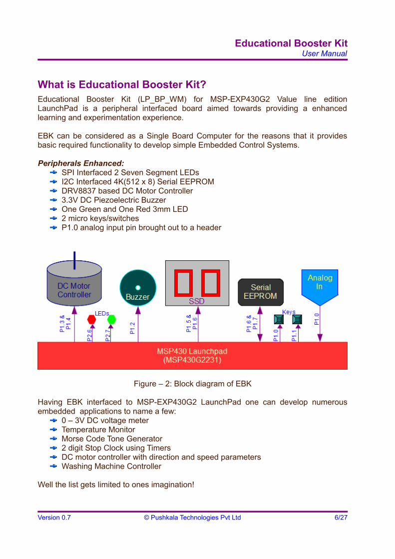
What is Educational Booster Kit?Educational Booster Kit (LP_BP_WM) for MSP-EXP430G2 Value line edition LaunchPad is a peripheral interfaced board aimed towards providing a enhanced learning and experimentation experience.
EBK can be considered as a Single Board Computer for the reasons that it provides basic required functionality to develop simple Embedded Control Systems.
Peripherals Enhanced:SPI Interfaced 2 Seven Segment LEDsI2C Interfaced 4K(512 x 8) Serial EEPROMDRV8837 based DC Motor Controller3.3V DC Piezoelectric BuzzerOne Green and One Red 3mm LED2 micro keys/switchesP1.0 analog input pin brought out to a header
Figure – 2: Block diagram of EBK
Having EBK interfaced to MSP-EXP430G2 LaunchPad one can develop numerous embedded applications to name a few:
0 – 3V DC voltage meterTemperature MonitorMorse Code Tone Generator2 digit Stop Clock using TimersDC motor controller with direction and speed parametersWashing Machine Controller
Well the list gets limited to ones imagination!
Version 0.7 © Pushkala Technologies Pvt Ltd 6/27

Educational Booster KitUser Manual
Identifying what is on EBK boardFigure 3 is the top side view of LP_BP_WM Rev 1.1A, and the accompanying legends identifies the main components on board.
Figure – 3: Top view of LP_BP_WM board
Version 0.7 © Pushkala Technologies Pvt Ltd 7/27
1
2
3 4
5 6
789
10 11
12
12

Educational Booster KitUser Manual
Legend # Description1 10 Pin Female Header which will snap into MSP-EXP430G2 LaunchPad2 Micro push button switches Key – 1 and Key – 2 3 Red LED – 3mm4 Green LED – 3mm5 Seven Segment LED modules6 Serial EEPROM IC7 Piezoelectric Buzzer8 DRV8837 DC motor controller IC9 DC motor connector10 Jumper 2[JP2] Supply Voltage to motor controller11 Jumper 1[JP1] Enable/Disable motor controller12 ADC Port/Connector
Figure – 4: Bottom view of LP_BP_WM board
Version 0.7 © Pushkala Technologies Pvt Ltd 8/27
11

Educational Booster KitUser Manual
Basic Development Setup
(Laptop, Launchpad and EBK image pending)Figure – 5: Setup of cross development environment.
Setting up development environment is very simple, follow these steps:
Disengage P1.0 and P1.6 jumpers on MSP-EXP430G2 LaunchPad board.
Plugin the EBK on to MSP-EXP430G2. If you have purchased EBK and MSP-EXP430G2 Launchpad separately, make sure you solder the header pins.Warning!: Checkout for the LP_BP_WM board orientation before plunging in.
Plug in the supplied USB Cable's one end to MSP-EXP430G2 LaunchPad, and the other end to PC/Laptop USB port.
MSP-EXP430G2 LaunchPad and EBK powers from the 5VDC available from USB, hence no additional power supply required.
Read through further sections to know about software required for cross development and a quick test scenario.
Note: MSP-EXP430G2 LaunchPad and EBK are not recommended to be connected to external USB Hubs.
Version 0.7 © Pushkala Technologies Pvt Ltd 9/27

Educational Booster KitUser Manual
Quick CheckThis section describes about how to test your EBK on first power up.
1. Connect the EBK as per the guidelines given in the previous section.2. Download, install, and open latest version of Code Composer Studio form TI
website.3. Download EBK_Test_V1 source code archive from www.pushkala.in EBK web
page. 4. Open, build, and debug EBK_Test_V1 project in CCS.5. You should see SSDs displaying “On”.6. Now press Key – 1 light Red LED and press Key – 2 to light Green LED.
This completes the quick test procedure, to explore all other available peripherals browse through respective sections of this document.
If in any case you do not succeed with the above steps immediately contact [email protected] and report the problem. Make sure your email subject is specified as EBK:<problem in short>.
Version 0.7 © Pushkala Technologies Pvt Ltd 10/27

Educational Booster KitUser Manual
Software Setup
Compiler and Debugger There are many cross compilers available for MSP430 family of microcontrollers.TI's own solution is Code Composer Studio and you can download from TI's website.
Tip: You may wish to install only MSP430 development environment
Note: Usage of a cross compiler, CCS or developing MSP430 programs in C or assembly is beyond the scope of this document. Refer to Useful Information section of this document to get related information.
Version 0.7 © Pushkala Technologies Pvt Ltd 11/27

Educational Booster KitUser Manual
First Program on EBK
Developing and Debugging a simple LED toggling code – BlinkyEBK comes with two general purpose LEDs RED and GREEN connected to MSP430 ports P2.6 and P2.7 respectively(Refer to Schematic section for details). Logic 1 written to respective port pins switched on the LED and Logic 0 switches off the same following code snippet demonstrates the operation. Make sure while using LEDs on Port 2 disable the multiplexed peripherals using Port2 Function Select Register P2SEL.
Step – 1: Create Project in your favorite MSP430 compilerStep – 2: Key in this code snippet in main.c
//**************************************************************// EBK LED Demo - Software Toggle P2.7// Description; Toggle P2.7 by xoring P2.7 forever// Default Clock Source//// Pushkala Technologies, India// www.pushkala.in// October 2012// Built with CCS Version 5.1.1 //**************************************************************
#include <msp430G2231.h>
void main(void){
volatile unsigned long delay = 0;
WDTCTL = WDTPW + WDTHOLD; // Stop watchdog timer
P2DIR |= BIT7; // Set P2.7 to output directionP2SEL = 0x00; //Clear multiplexed function in P2
while(1) {
P2OUT ^= BIT7;for(delay = 0; delay < 65534; delay++); //SW Delay
}}
Step – 3: Build the project and run. On successful execution you will observe that Green LED toggling.
Version 0.7 © Pushkala Technologies Pvt Ltd 12/27

Educational Booster KitUser Manual
Jumper settingsThere are two Jumpers[JP1 & JP2] to configure DC motor controller on LP_BP_WM board.
These jumpers are two pin variants. In figure below the black thick line on pad pin represent the presence of a short link. Short link is simple two pin conductive connector. Short links are provided for all jumpers.
Figure – 8: Jumper connection schemes
Jumper 1[JP1]: Enable/Disable DRV8837 DC Motor Controller.
Standard Setting: Enabled
Short link between Pin 1 and 2 EnabledNo short link between Pin 1 and 2 Disabled
Jumper 2[JP2]: Provide/Remove DC supply voltage to DRV8837.
This jumper is used to derive DC supply voltage to motor controller from Launchpad or external source. If a high current motor is used other than the one supplied along with EBK one may remove JP2 and provide external voltage on pin 2(closer to DRV8837) of JP2.
Note: Do not exceed 7VDC external DC voltage to DRV8837, else the device may be damaged permanently.
Standard Setting: LaunchPad Supply
Short link between Pin 1 and 2 Launchpad SourceNo short link between Pin 1 and 2 External Source
Version 0.7 © Pushkala Technologies Pvt Ltd 13/27
No short link b/w Pin 1 & 2 Short link b/w Pin 1 & 2

Educational Booster KitUser Manual
Key1 and Key2 InputsTwo micro switch key inputs are provided on EBK mapped to Port1 pins P1.0 and P1.1.Refer to Schematic section for more details. P1.0 pin is also mapped as Analog input pin in EBK and hence P1SEL register configuration should be considered for usage as Digital Input.
Following code demonstrates the usage of P1.0 as input pin.
//**************************************************************// EBK Key1 Demo – P1.0 as Key1 input // Description; RED LED glows when Key1 is pressed// Default Clock Source//// Pushkala Technologies, India// www.pushkala.in// October 2012// Built with CCS Version 5.1.1 //**************************************************************
#include <msp430G2231.h>
void main(void){
WDTCTL = WDTPW + WDTHOLD; // Stop watchdog timer
P1DIR &= ~BIT0; //Clear P1DIR.0 to set P1.0 as inputP1REN |= BIT0; //Enable pullup resistor on P1.0P1SEL = 0x00;
P2DIR |= BIT7; // Set P2.7 to output directionP2SEL = 0x00; //Clear multiplexed function in P2
while(1) {
if(!(P1IN & BIT0))P2OUT |= BIT7;
elseP2OUT &= ~BIT7;
}}
Version 0.7 © Pushkala Technologies Pvt Ltd 14/27

Educational Booster KitUser Manual
Seven Segment DisplayEBK comes with two seven segment red LED displays driven by two serial in parallel out shift registers connected in series. First shift register's(driving DIS1) data input is connected to port P1.6 of uC which also SDO signal of SPI group. P1.5 is used as SCLK or serial clock. Refer schematics for hardware details. Display data is serially transferred as two byte information corresponding to DIS1 and DIS2, first byte corresponding to DIS2.
Following code demonstrates a free running counter application.
//**************************************************************// EBK SSD Demo – Display 0.0 to 9.9 count// Description; Free running software counter with software delay// Default Clock Source//// Pushkala Technologies, India// www.pushkala.in// October 2012// Built with CCS Version 5.1.1//*
#include <msp430g2231.h>
#define DLY 100000
#define LED_PORT P1OUT#define LED1_ON() (LED_PORT |= BIT0)#define LED1_OFF() (LED_PORT &= ~BIT0)
#define SPI_PORT P1OUT#define SET_SPI_PORT(x) (SPI_PORT |= x)#define CLR_SPI_PORT(x) (SPI_PORT &= ~x)#define SPI_SCK BIT5#define SPI_SDO BIT6#define BUZ BIT2
#define DP 0x80 //Decimal point
const unsigned char ssd[10] = {0x3f, 0x06, 0x5B, 0x4F, 0x66, 0x6D, 0x7D, 0x07, 0x7F, 0x6F};
void transferToSSD(unsigned char digit1, unsigned short digit2);void swDelay(volatile unsigned long Delay);
Version 0.7 © Pushkala Technologies Pvt Ltd 15/27

Educational Booster KitUser Manual
void main(void){
unsigned short dispU = 0, dispT = 0;unsigned short count = 0x0000;
WDTCTL = WDTPW + WDTHOLD; // Stop watchdog timer
P1DIR = 0xEC; // Set P1 direction 1 = Out 0 = In
CLR_SPI_PORT(SPI_SDO);CLR_SPI_PORT(SPI_SCK);CLR_SPI_PORT(BUZ);
LED1_OFF();
/*Forever*/
while(1){
dispU = count % 10; //Process the data for displaydispT = count / 10;
transferToSSD(ssd[dispU], (ssd[dispT] | DP)); //Enable decimal/dot point for tens place
count++;if(count > 99)
count = 0;
swDelay(DLY);
}
}
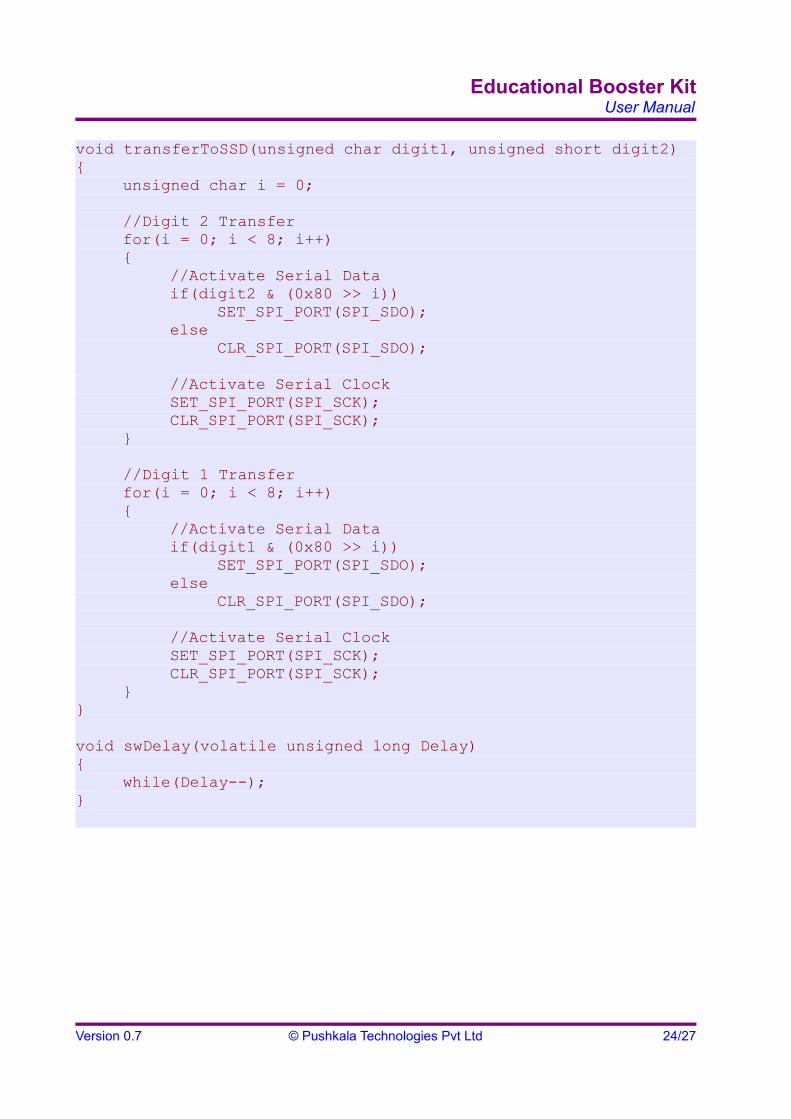
void transferToSSD(unsigned char digit1, unsigned short digit2){
unsigned char i = 0;
//Digit 2 Transferfor(i = 0; i < 8; i++){
//Activate Serial Dataif(digit2 & (0x80 >> i))
Version 0.7 © Pushkala Technologies Pvt Ltd 16/27

Educational Booster KitUser Manual
SET_SPI_PORT(SPI_SDO);else
CLR_SPI_PORT(SPI_SDO);
//Activate Serial ClockSET_SPI_PORT(SPI_SCK);CLR_SPI_PORT(SPI_SCK);
}
//Digit 1 Transferfor(i = 0; i < 8; i++){
//Activate Serial Dataif(digit1 & (0x80 >> i))
SET_SPI_PORT(SPI_SDO);else
CLR_SPI_PORT(SPI_SDO);
//Activate Serial ClockSET_SPI_PORT(SPI_SCK);CLR_SPI_PORT(SPI_SCK);
}
}
void swDelay(volatile unsigned long Delay){
while(Delay--);}
Version 0.7 © Pushkala Technologies Pvt Ltd 17/27
Educational Booster KitUser Manual
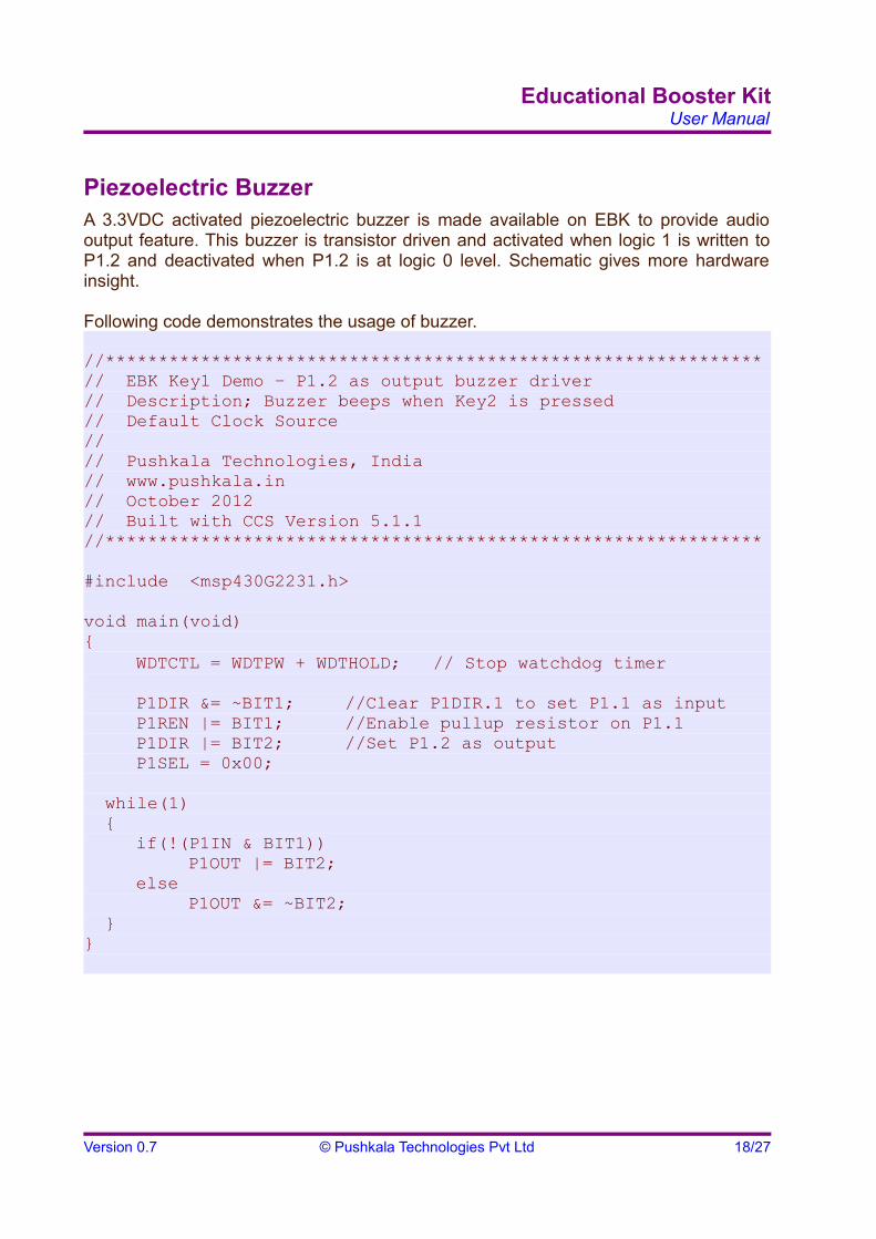
Piezoelectric BuzzerA 3.3VDC activated piezoelectric buzzer is made available on EBK to provide audio output feature. This buzzer is transistor driven and activated when logic 1 is written to P1.2 and deactivated when P1.2 is at logic 0 level. Schematic gives more hardware insight.
Following code demonstrates the usage of buzzer.
//**************************************************************// EBK Key1 Demo – P1.2 as output buzzer driver// Description; Buzzer beeps when Key2 is pressed// Default Clock Source//// Pushkala Technologies, India// www.pushkala.in// October 2012// Built with CCS Version 5.1.1 //**************************************************************
#include <msp430G2231.h>
void main(void){
WDTCTL = WDTPW + WDTHOLD; // Stop watchdog timer
P1DIR &= ~BIT1; //Clear P1DIR.1 to set P1.1 as inputP1REN |= BIT1; //Enable pullup resistor on P1.1P1DIR |= BIT2; //Set P1.2 as outputP1SEL = 0x00;
while(1) {
if(!(P1IN & BIT1))P1OUT |= BIT2;
elseP1OUT &= ~BIT2;
}}
Version 0.7 © Pushkala Technologies Pvt Ltd 18/27

Educational Booster KitUser Manual
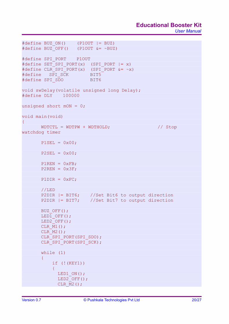
DC Motor ControllerA brushed DC motor which can operate at 3.3VDC can be controlled through EBK. TI's DRV8837 bidirectional DC motor controller IC is interfaced to MSP430. Further details can be derived from EBK's schematic and DRV8837 data sheet. Refer to Jumper Section of this document for more information on configuration of DC motor controller.
Note: Do not connect the motor while downloading the firmware to Launchpad, or disengage Jumper JP1 or JP2 to disable motor. Motor is a heavy inductive load and may consume more power during start-up time and this will lead to USB re-enumeration of Launchpad few a times.
Following code demonstrates bidirectional control of motor.
//**************************************************************// EBK Motor Demo – DC motor controller// Description; Pressing Key-2 starts the motor in clock wise// direction and same key again stops the motor// Key-1 is configured to start and stop the motor// in counter clock wise direction.// Default Clock Source//// Pushkala Technologies, India// www.pushkala.in// October 2012// Built with CCS Version 5.1.1//**************************************************************#include <msp430G2231.h>
#define LED_PORT P2OUT#define LED1_ON() (LED_PORT |= BIT6)#define LED1_OFF() (LED_PORT &= ~BIT6)#define LED2_ON() (LED_PORT |= BIT7)#define LED2_OFF() (LED_PORT &= ~BIT7)
#define KEY1 (P1IN & BIT0)#define KEY2 (P1IN & BIT1)
#define M1 BIT3#define M2 BIT4#define SET_M1() (P1OUT |= M1)#define SET_M2() (P1OUT |= M2)#define CLR_M1() (P1OUT &= ~M1)#define CLR_M2() (P1OUT &= ~M2)
#define BUZ BIT2
Version 0.7 © Pushkala Technologies Pvt Ltd 19/27
Educational Booster KitUser Manual
#define BUZ_ON() (P1OUT |= BUZ)#define BUZ_OFF() (P1OUT &= ~BUZ)
#define SPI_PORT P1OUT#define SET_SPI_PORT(x) (SPI_PORT |= x)#define CLR_SPI_PORT(x) (SPI_PORT &= ~x)#define SPI_SCK BIT5#define SPI_SDO BIT6
void swDelay(volatile unsigned long Delay);#define DLY 100000
unsigned short mON = 0;
void main(void){
WDTCTL = WDTPW + WDTHOLD; // Stop watchdog timer
P1SEL = 0x00;
P2SEL = 0x00;
P1REN = 0xFB; P2REN = 0x3F;
P1DIR = 0xFC;
//LED P2DIR |= BIT6; //Set Bit6 to output direction P2DIR |= BIT7; //Set Bit7 to output direction
BUZ_OFF(); LED1_OFF(); LED2_OFF(); CLR_M1(); CLR_M2(); CLR_SPI_PORT(SPI_SDO); CLR_SPI_PORT(SPI_SCK);
while (1) { if (!(KEY1)) { LED1_ON(); LED2_OFF(); CLR_M2();
Version 0.7 © Pushkala Technologies Pvt Ltd 20/27

Educational Booster KitUser Manual
CLR_M1(); swDelay(DLY); if(mON) { CLR_M1(); CLR_M2(); mON = 0; } else { SET_M1(); mON = 1; } }
if (!(KEY2)) { LED2_ON(); LED1_OFF(); CLR_M1(); CLR_M2(); swDelay(DLY); if(mON) { CLR_M1(); CLR_M2(); mON = 0; } else { SET_M2(); mON = 1; }
}
}}
void swDelay(volatile unsigned long Delay){
while(Delay--);}
Version 0.7 © Pushkala Technologies Pvt Ltd 21/27

Educational Booster KitUser Manual
Analog InputMSP430G2231 controller supplied with Launchpad kit has eight 10 bit ADC channels multiplexed to operate with Port 1 pins. Among these P1.0 that is Analog input Channel-0 or A0 is brought out on to a connector on LP_BP_WM board. Legend 12 on Figure 3 represents the connector. On either side of the connector you will find 3.3VDC and GND signals made available. Standard 3 pin potentiometer or Temperature Sensors and any similar analog signals can be connected to this pin. Voltage reference for the ADC is derived from microcontroller's internal sources. More details on usage of ADC is available in MSP430G2231's family user guide.
Note: Do not apply voltage lees than 0VDC or greater than 3.3VDC to analog input pin.
Following is volt meter demonstration code.
//**************************************************************// EBK Analog in Demo – 0 to 3.2VDC Volt meter solution// Description; P1.0 configured as analog input pin// Voltage input variance on P1.0 is reflected as// two digit valuse on SSD// Default Clock Source//// Pushkala Technologies, India// www.pushkala.in// October 2012// Built with CCS Version 5.1.1//**************************************************************
#include <msp430g2231.h>
#define DLY 100000
#define LED_PORT P1OUT#define LED1_ON() (LED_PORT |= BIT0)#define LED1_OFF() (LED_PORT &= ~BIT0)
#define SPI_PORT P1OUT#define SET_SPI_PORT(x) (SPI_PORT |= x)#define CLR_SPI_PORT(x) (SPI_PORT &= ~x)#define SPI_SCK BIT5#define SPI_SDO BIT6#define BUZ BIT2
#define DP 0x80
const unsigned char ssd[10] = {0x3f, 0x06, 0x5B, 0x4F, 0x66,
Version 0.7 © Pushkala Technologies Pvt Ltd 22/27

Educational Booster KitUser Manual
0x6D, 0x7D, 0x07, 0x7F, 0x6F};
void transferToSSD(unsigned char digit1, unsigned short digit2);void swDelay(volatile unsigned long Delay);
void main(void){
unsigned short adcU = 0, adcT = 0;unsigned long adcData = 0x00000000;
WDTCTL = WDTPW + WDTHOLD; // Stop watchdog timer
P1DIR = 0xEC; // Set P1 direction 1 = Out 0 = In
CLR_SPI_PORT(SPI_SDO);CLR_SPI_PORT(SPI_SCK);CLR_SPI_PORT(BUZ);
LED1_OFF();
/*ADC Forever*/while(1){//ADC ConfigurationADC10AE0 = 0x0001; //Make A0 of P1.0 bit AnalogADC10MEM = 0x0000; //Clear ADC data registerADC10CTL0 = 0x0000;ADC10CTL0 |= ADC10SHT1 | ADC10SHT0 | ADC10ON; //VCC VrefADC10CTL1 |= INCH_0;ADC10CTL0 |= ENC;ADC10CTL0 |= ADC10SC; //Start Conversion
while(ADC10CTL1 & ADC10BUSY);
ADC10AE0 = 0x0000; //Make A0 of P1.0 bit digital
adcData = ADC10MEM; //Get ADCed dataadcData *= 322; //Multiply by ADC step size * 100000adcData /= 10000; //Correct the value for 2 digit precisionadcU = adcData % 10; //Process the data for displayadcT = adcData / 10;
transferToSSD(ssd[adcU], (ssd[adcT] | DP));
swDelay(DLY);}
}
Version 0.7 © Pushkala Technologies Pvt Ltd 23/27
Educational Booster KitUser Manual
void transferToSSD(unsigned char digit1, unsigned short digit2){
unsigned char i = 0;
//Digit 2 Transferfor(i = 0; i < 8; i++){
//Activate Serial Dataif(digit2 & (0x80 >> i))
SET_SPI_PORT(SPI_SDO);else
CLR_SPI_PORT(SPI_SDO);
//Activate Serial ClockSET_SPI_PORT(SPI_SCK);CLR_SPI_PORT(SPI_SCK);
}
//Digit 1 Transferfor(i = 0; i < 8; i++){
//Activate Serial Dataif(digit1 & (0x80 >> i))
SET_SPI_PORT(SPI_SDO);else
CLR_SPI_PORT(SPI_SDO);
//Activate Serial ClockSET_SPI_PORT(SPI_SCK);CLR_SPI_PORT(SPI_SCK);
}}
void swDelay(volatile unsigned long Delay){
while(Delay--);}
Version 0.7 © Pushkala Technologies Pvt Ltd 24/27

Educational Booster KitUser Manual
Schematic
Figure – 10: SSD Schematic.
Version 0.7 © Pushkala Technologies Pvt Ltd 25/27

Educational Booster KitUser Manual
Figure – 11: Other Section's Schematic.
Version 0.7 © Pushkala Technologies Pvt Ltd 26/27

Educational Booster KitUser Manual
Contacts
Technical : [email protected]
Sales : [email protected]
Generic : [email protected]
Website : www.pushkala.in Postal Address : Pushkala Technologies Pvt Ltd
No. 38, "SHREEKANTA", West Anjaneya Temple Street, Basavanagudi, Bangalore – 560004Karnataka, India
Version 0.7 © Pushkala Technologies Pvt Ltd 27/27