Edit DATA SHEET OTM8009A V08 20120222€¦ · 2019-04-19 · ORISE Technology reserves the right to...
297
ORISE Technology reserves the right to change this documentation without prior notice. Information provided by ORISE Technology is believed to be accurate and reliable. However, ORISE Technology makes no warranty for any errors which may appear in this document. Contact ORISE Technology to obtain the latest version of device specifications before placing your order. No responsibility is assumed by ORISE Technology for any infringement of patent or other rights of third parties which may result from its use. In addition, ORISE Technology products are not authorized for use as critical components in life support devices/ systems or aviation devices/systems, where a malfunction or failure of the product may reasonably be expected to result in significant injury to the user, without the express written approval of ORISE Technology. Preliminary FEB. 22, 2012 Version 0.8 O O T T M M 8 8 0 0 0 0 9 9 A A 1440-channel 8-bit Source Driver and 864 Gate Driver with System-on-chip for Color Amorphous TFT-LCDs ORISE Tech Confidential For IVO Use Only
Transcript of Edit DATA SHEET OTM8009A V08 20120222€¦ · 2019-04-19 · ORISE Technology reserves the right to...

ORISE Technology reserves the right to change this documentation without prior notice. Information provided by ORISE Technology is believed to be
accurate and reliable. However, ORISE Technology makes no warranty for any errors which may appear in this document. Contact ORISE Technology to
obtain the latest version of device specifications before placing your order. No responsibility is assumed by ORISE Technology for any infringement of patent
or other rights of third parties which may result from its use. In addition, ORISE Technology products are not authorized for use as critical components in life
support devices/ systems or aviation devices/systems, where a malfunction or failure of the product may reasonably be expected to result in significant injury to
the user, without the express written approval of ORISE Technology.
PPrreelliimmiinnaarryy
FEB. 22, 2012
Version 0.8
OOTTMM88000099AA
11444400--cchhaannnneell 88--bbiitt SSoouurrccee DDrriivveerr aanndd
886644 GGaattee DDrriivveerr wwiitthh SSyysstteemm--oonn--cchhiipp
ffoorr CCoolloorr AAmmoorrpphhoouuss TTFFTT--LLCCDDss
ORISE Tec
h Con
fiden
tial
For IV
O Use
Only

PPrreelliimmiinnaarryy
OTM8009A
© ORISE Technology Co., Ltd.
Proprietary & Confidential
2 FEB.22 2012
Preliminary Version 0.8
Table of Contents PAGE
1. GENERAL DESCRIPTION .......................................................................................................................................................................... 8 2. FEATURES .................................................................................................................................................................................................. 8 3. BLOCK DIAGRAM ....................................................................................................................................................................................... 9
3.1. BLOCK FUNCTION .................................................................................................................................................................................. 9 3.1.1. System interface................................................................................................................................................................... 10 3.1.2. Address Counter (AC) .......................................................................................................................................................... 10 3.1.3. Graphics RAM (GRAM)........................................................................................................................................................ 10 3.1.4. Grayscale voltage generating circuit .................................................................................................................................... 10 3.1.5. Timing controller ................................................................................................................................................................... 10 3.1.6. Oscillator (OSC) ................................................................................................................................................................... 10 3.1.7. Source driver circuit.............................................................................................................................................................. 10 3.1.8. Gate driver circuit ................................................................................................................................................................. 10 3.1.9. LCD driving power supply circuit .......................................................................................................................................... 10
3.2. GAMMA CORRECTION CIRCUIT ..............................................................................................................................................................11 3.2.1. Positive gamma correction circuit..........................................................................................................................................11 3.2.2. Negative gamma correction circuit ....................................................................................................................................... 12
4. SIGNAL DESCRIPTIONS .......................................................................................................................................................................... 13 4.1. PIN DEFINITION.................................................................................................................................................................................... 13 4.2. POWER ARCHITECTURE ....................................................................................................................................................................... 18 4.3. POWER SUPPLY CONFIGURATION ......................................................................................................................................................... 19 4.4. BOM LIST ........................................................................................................................................................................................... 20
5. INSTRUCTIONS........................................................................................................................................................................................ 21 5.1. OUTLINE.............................................................................................................................................................................................. 21
5.1.1. System function command list and description .................................................................................................................... 22 5.2. SYSTEM COMMAND DESCRIPTION ........................................................................................................................................................ 26
5.2.1. NOP (00h): No Operation..................................................................................................................................................... 26 5.2.2. SWRESET (01h): Software Reset........................................................................................................................................ 27 5.2.3. RDNUMED (05H) Read Number of the Errors on DSI......................................................................................................... 28 5.2.4. RDDPM (0AH): Read Display Power Mode ......................................................................................................................... 29 5.2.5. RDDMADCTR (0BH): Read Display MADCTR.................................................................................................................... 30 5.2.6. RDDCOLMOD (0CH): Read Display Pixel Format .............................................................................................................. 31 5.2.7. RDDIM (0DH): Read Display Image Mode .......................................................................................................................... 32 5.2.8. RDDSM (0EH): Read Display Signal Mode ......................................................................................................................... 33 5.2.9. RDDSDR (0FH): Read Display Self-Diagnostic Result ........................................................................................................ 34 5.2.10. SLPIN (10H): Sleep In.......................................................................................................................................................... 35 5.2.11. SLPOUT (11H): Sleep Out ................................................................................................................................................... 36 5.2.12. PTLON (12H): Partial Display Mode On............................................................................................................................... 37 5.2.13. NORON (13H): Normal Display Mode On............................................................................................................................ 38 5.2.14. INVOFF (20h) : Display Inversion Off................................................................................................................................... 39 5.2.15. INVON (21h) : Display Inversion On .................................................................................................................................... 40 5.2.16. ALLPOFF (22H): All Pixels Off ............................................................................................................................................. 41 5.2.17. ALLPON (23H): All Pixels On............................................................................................................................................... 42 5.2.18. GAMSET (26H): Gamma Set ............................................................................................................................................... 43
ORISE Tec
h Con
fiden
tial
For IV
O Use
Only
PPrreelliimmiinnaarryy
OTM8009A
© ORISE Technology Co., Ltd.
Proprietary & Confidential
3 FEB.22 2012
Preliminary Version 0.8
5.2.19. DISPOFF (28H): Display Off ................................................................................................................................................ 44 5.2.20. DISPON (29H): Display On.................................................................................................................................................. 45 5.2.21. CASET (2AH): Column Address Set .................................................................................................................................... 46 5.2.22. PASET (2BH): Page Address Set......................................................................................................................................... 48 5.2.23. RAMWR (2CH): Memory Write ............................................................................................................................................ 50 5.2.24. RAMRD (2EH): Memory Read ............................................................................................................................................. 51 5.2.25. PTLAR (30H): Partial Area ................................................................................................................................................... 52 5.2.26. TEOFF (34H): Tearing Effect Line OFF................................................................................................................................ 54 5.2.27. TEON (35H): Tearing Effect Line ON ................................................................................................................................... 55 5.2.28. MADCTR (36H): Memory Data Access Control ................................................................................................................... 56 5.2.29. IDMOFF (38H): Idle Mode Off .............................................................................................................................................. 58 5.2.30. IDMON (39H): Idle Mode On................................................................................................................................................ 59 5.2.31. COLMOD (3AH): Interface Pixel Format .............................................................................................................................. 60 5.2.32. RAMWRCNT (3CH): Memory Write Continue...................................................................................................................... 61 5.2.33. RAMRDCNT (3EH): Memory Read Continue ...................................................................................................................... 62 5.2.34. WRTESCN (44H): Write TE Scan Line ................................................................................................................................ 63 5.2.35. RDSCNL (45H): Read Scan Line ......................................................................................................................................... 64 5.2.36. WRDISBV (51H) Write Display Brightness .......................................................................................................................... 65 5.2.37. RDDISBV (52H) Read Display Brightness Value................................................................................................................. 66 5.2.38. WRCTRLD (53H) Write CTRL Display................................................................................................................................. 67 5.2.39. RDCTRLD (54H) Read CTRL Display ................................................................................................................................. 68 5.2.40. WRCABC (55H) Write Content Adaptive Brightness Control............................................................................................... 69 5.2.41. RDCABC (56H) Read Content Adaptive Brightness Control ............................................................................................... 70 5.2.42. WRCABCMB (5EH) Write CABC Minimum Brightness........................................................................................................ 71 5.2.43. RDCABCMB (5FH) Read CABC Minimum Brightness ........................................................................................................ 72 5.2.44. RDPWMSDR (68H) Read Automatic Brightness Control Self-diagnostics Result............................................................... 73 5.2.45. RDBWLB (70H) Read Back/White Low Bits......................................................................................................................... 74 5.2.46. RDBkx (71H) Read Bkx........................................................................................................................................................ 75 5.2.47. RDBky (72H) Read Bky........................................................................................................................................................ 75 5.2.48. RDWx (73H) Read Wx ......................................................................................................................................................... 76 5.2.49. RDWy (74H) Read Wy ......................................................................................................................................................... 76 5.2.50. RDRGLB (75H) Read Red/Green Low Bits.......................................................................................................................... 77 5.2.51. RDRx (76H) Read Rx........................................................................................................................................................... 78 5.2.52. RDRy (77H) Read Ry........................................................................................................................................................... 78 5.2.53. RDGx (78H) Read Gx .......................................................................................................................................................... 79 5.2.54. RDGy (79H) Read Gy .......................................................................................................................................................... 79 5.2.55. RDBALB (7AH) Read Blue/AColour Low Bits ...................................................................................................................... 80 5.2.56. RDBx (7BH) Read Bx........................................................................................................................................................... 81 5.2.57. RDBy (7CH) Read By........................................................................................................................................................... 81 5.2.58. RDAx (7DH) Read Ax........................................................................................................................................................... 82 5.2.59. RDAy (7EH) Read Ay ........................................................................................................................................................... 82 5.2.60. RDDDBSTR (A1H): Read DDB Start ................................................................................................................................... 83 5.2.61. RDDDBCNT (A8H): Read DDB Continue ............................................................................................................................ 84 5.2.62. RDFCS (AAH): Read First Checksum.................................................................................................................................. 85 5.2.63. RDCCS (AFH): Read Continue Checksum.......................................................................................................................... 86
ORISE Tec
h Con
fiden
tial
For IV
O Use
Only

PPrreelliimmiinnaarryy
OTM8009A
© ORISE Technology Co., Ltd.
Proprietary & Confidential
4 FEB.22 2012
Preliminary Version 0.8
5.2.64. RDID1 (DAH): Read ID1 ...................................................................................................................................................... 86 5.2.65. RDID2 (DBH): Read ID2 ...................................................................................................................................................... 87 5.2.66. RDID3 (DCH): Read ID3 ...................................................................................................................................................... 87
5.3. CUSTOMER COMMAND LIST AND DESCRIPTION (MANUFACTURER COMMAND SET / COMMAND 2) ............................................................ 88 5.3.1. ADRSFT (0000h): Address Shift Function............................................................................................................................ 89 5.3.2. CMD2_ENA1 (FF00h): Enable Access Command 2 & Software EXTC Enable .................................................................. 90 5.3.3. CMD2_ENA2 (FF80h): Enable Access Orise Command 2 .................................................................................................. 90 5.3.4. OTPSEL (A000h): Gamma 2.2 OTP Select Region............................................................................................................. 91 5.3.5. MIPISET1 (B080h): MIPI Setting 1....................................................................................................................................... 92 5.3.6. MIPISET2 (B0B2h): MIPI Setting 2 ...................................................................................................................................... 93 5.3.7. IF_PARA1 (B280H) IF Parameter 1...................................................................................................................................... 94 5.3.8. IF_PARA2 (B282H) IF Parameter 2...................................................................................................................................... 95 5.3.9. PAD_PARA (B390H) IOPAD Parameter................................................................................................................................ 98 5.3.10. PANSET (B3A6h): Panel Type Setting................................................................................................................................. 99 5.3.11. RAMPWRSET (B3C0h): SRAM Power Setting.................................................................................................................. 100 5.3.12. TSP1(C080h) TCON Setting Parameter 1 ......................................................................................................................... 101 5.3.13. PTSP1(C092h) Panel Timing Setting Parameter 1 ............................................................................................................... 102 5.3.14. PTSP2 (C094h) Panel Timing Setting Parameter 2 .............................................................................................................. 103 5.3.15. SD_CTRL (C0A2h) Source Driver Timing Setting ................................................................................................................ 104 5.3.16. P_DRV_M(C0B4h) : Panel Driving Mode........................................................................................................................... 105 5.3.17. OSC_ADJ(C181h) : Oscillator Adjustment for Idle/Normal Mode ...................................................................................... 106 5.3.18. RGB_VIDEO_SET(C1A1h): RGB Video Mode Setting.......................................................................................................... 107 5.3.19. SD_PCH_CTRL(C480h): Source Driver Precharge Control................................................................................................... 109 5.3.20. PWR_CTRL1(C580h): Power Control Setting 1 .....................................................................................................................110 5.3.21. PWR_CTRL2(C590h): Power Control Setting 2 for Normal Mode......................................................................................112 5.3.22. PWR_CTRL3(C5A0h): Power Control Setting 3 for Idle Mode ...........................................................................................116 5.3.23. PWR_CTRL4(C5B0h): Power Control Setting 4 for DC Voltage Settings.......................................................................... 120 5.3.24. PWM_PARA1 (C680H) PWM Parameter 1........................................................................................................................... 122 5.3.25. PWM_PARA2 (C6B0H) PWM Parameter 2 ........................................................................................................................ 123 5.3.26. PWM_PARA3 (C6B1H) PWM Parameter 3 ........................................................................................................................ 124 5.3.27. PWM_PARA4 (C6B3H) PWM Parameter 4 ........................................................................................................................ 126 5.3.28. PWM_PARA5 (C6B4H) PWM Parameter 5 .......................................................................................................................... 127 5.3.29. PWM_PARA6 (C6B5H) PWM Parameter 6 ........................................................................................................................ 128 5.3.30. CABCSET1 (C700h): CABC Setting..................................................................................................................................... 129 5.3.31. CABCSET2 (C800h): CABC gamma curve setting................................................................................................................ 130 5.3.32. AIESET(C900h): AIE Setting.............................................................................................................................................. 131 5.3.33. GOAVST(CE80h~CE8Bh) GOA VST Setting..................................................................................................................... 132 5.3.34. GOAVEND(CE90h~CE9Bh) GOA VEND Setting............................................................................................................... 133 5.3.35. GOAGPSET(CE9Ch~CE9Dh) GOA Group Setting ........................................................................................................... 134 5.3.36. GOACLKA1(CEA0h~CEA6h) GOA CLKA1 Setting ........................................................................................................... 135 5.3.37. GOACLKA2(CEA7h~CEADh) GOA CLKA2 Setting........................................................................................................... 137 5.3.38. GOACLKA3(CEB0h~CEB6h) GOA CLKA3 Setting ........................................................................................................... 138 5.3.39. GOACLKA4(CEB7h~CEBDh) GOA CLKA4 Setting........................................................................................................... 139 5.3.40. GOACLKB1(CEC0h~CEC6h) GOA CLKB1 Setting........................................................................................................... 140 5.3.41. GOACLKB2(CEC7h~CECDh) GOA CLKB2 Setting .......................................................................................................... 141
ORISE Tec
h Con
fiden
tial
For IV
O Use
Only

PPrreelliimmiinnaarryy
OTM8009A
© ORISE Technology Co., Ltd.
Proprietary & Confidential
5 FEB.22 2012
Preliminary Version 0.8
5.3.42. GOACLKB3(CED0h~CED6h) GOA CLKB3 Setting........................................................................................................... 142 5.3.43. GOACLKB4(CED7h~CEDDh) GOA CLKB4 Setting .......................................................................................................... 143 5.3.44. GOACLKC1(CF80h~CF86h) GOA CLKC1 Setting ............................................................................................................ 144 5.3.45. GOACLKC2(CF87h~CF8Dh) GOA CLKC2 Setting ........................................................................................................... 145 5.3.46. GOACLKC3(CF90h~CF96h) GOA CLKC3 Setting ............................................................................................................ 146 5.3.47. GOACLKC4(CF97h~CF9Dh) GOA CLKC4 Setting ........................................................................................................... 147 5.3.48. GOACLKD1(CFA0h~CFA6h) GOA CLKD1 Setting............................................................................................................ 148 5.3.49. GOACLKD2(CFA7h~CFADh) GOA CLKD2 Setting ........................................................................................................... 149 5.3.50. GOACLKD3(CFB0h~CFB6h) GOA CLKD3 Setting ........................................................................................................... 150 5.3.51. GOACLKD4(CFB7h~CFBDh) GOA CLKD4 Setting........................................................................................................... 151 5.3.52. GOAECLK(CFC0h~CFC5h) GOA ECLK Setting ............................................................................................................... 152 5.3.53. GOAOPT1(CFC6h) GOA Other Options 1 ......................................................................................................................... 154 5.3.54. GOATGOPT(CFC7h~CFC9h) GOA Signal Toggle Option Setting..................................................................................... 155 5.3.55. WRID1(D000h) ID1 Setting ................................................................................................................................................ 157 5.3.56. WRID2(D100h) ID2/ID3 Setting ......................................................................................................................................... 157 5.3.57. WRDDB(D200h) DDB Setting ............................................................................................................................................ 158 5.3.58. EXTCCHK (D300h): EXTC Check........................................................................................................................................ 159 5.3.59. CESET1 (D400h): CE Correction Characteristics Setting 1............................................................................................... 160 5.3.60. CESET2(D500h): CE Correction Characteristics Setting 2................................................................................................ 161 5.3.61. CEEN(D680h): CE Enable ................................................................................................................................................. 162 5.3.62. AIEEN(D700h): AIE Enable................................................................................................................................................ 163 5.3.63. GVDDSET (D800h): GVDD/NGVDD.................................................................................................................................... 164 5.3.64. VCOMDC (D900h): VCOM voltage setting............................................................................................................................ 165 5.3.65. GMCT2.2P (E100h): Gamma Correction Characteristics Setting (2.2 + ).......................................................................... 166 5.3.66. GMCT2.2N (E200h): Gamma Correction Characteristics Setting (2.2 - ) ................................................................................ 167 5.3.67. GMCT1.8P (E300h): Gamma Correction Characteristics Setting (1.8 + )................................................................................ 168 5.3.68. GMCT1.8N (E400h): Gamma Correction Characteristics Setting (1.8 - ) ................................................................................ 169 5.3.69. GMCT2.5P (E500h): Gamma Correction Characteristics Setting (2.5 + )................................................................................ 170 5.3.70. GMCT2.5N (E600h): Gamma Correction Characteristics Setting (2.5 - ) ................................................................................ 171 5.3.71. GMCT1.0N (E700h): Gamma Correction Characteristics Setting (1.0 + ) ............................................................................... 172 5.3.72. GMCT1.0N (E800h): Gamma Correction Characteristics Setting (1.0 - ) ................................................................................ 173 5.3.73. NVMIN (EB00h): NV Memory Write Mode ............................................................................................................................ 174 5.3.74. DGAMR (EC00h): Digital Gamma Correction Characteristics Setting (Red): .......................................................................... 175 5.3.75. DGAMR (ED00h): Digital Gamma Correction Characteristics Setting (Green): ....................................................................... 176 5.3.76. DGAMB (EE00h): Digital Gamma Correction Characteristics Setting (Blue): ..................................................................... 177 5.3.77. PRG_FLAG (F101h): OTP Program Flag Check ............................................................................................................... 178
6. FUNCTION DESCRIPTIONS................................................................................................................................................................... 179 6.1. INTERFACE TYPE SELECTION .............................................................................................................................................................. 179 6.2. MIPI-DSI INTERFACE ......................................................................................................................................................................... 180
6.2.1. General description ............................................................................................................................................................ 180 6.2.2. Interface level communication............................................................................................................................................ 180 6.2.3. DSI data lanes.................................................................................................................................................................... 185 6.2.4. Packet level communication............................................................................................................................................... 196 6.2.5. Customer-defined generic read data type format............................................................................................................... 207
6.3. MDDI INTERFACE .............................................................................................................................................................................. 208
ORISE Tec
h Con
fiden
tial
For IV
O Use
Only

PPrreelliimmiinnaarryy
OTM8009A
© ORISE Technology Co., Ltd.
Proprietary & Confidential
6 FEB.22 2012
Preliminary Version 0.8
6.3.1. General description ............................................................................................................................................................ 208 6.3.2. MDDI Packet summary ...................................................................................................................................................... 209 6.3.3. MDDI Packet format ........................................................................................................................................................... 209 6.3.4. Hibernation / wake-up ........................................................................................................................................................ 220
6.4. RGB INTERFACE................................................................................................................................................................................ 222 6.4.1. RGB interface color mapping Format................................................................................................................................. 222 6.4.2. RGB timing parameter........................................................................................................................................................ 223 6.4.3. RGB interface power on/off sequence ............................................................................................................................... 227
6.5. MPU-SERIES PARALLEL INTERFACE ................................................................................................................................................... 228 6.5.1. Write cycle sequence ......................................................................................................................................................... 228 6.5.2. Read cycle sequence......................................................................................................................................................... 229 6.5.3. MPU mode color coding..................................................................................................................................................... 231
6.6. I2C-BUS INTERFACE........................................................................................................................................................................... 236 6.6.1. Characteristics of I2C-bus................................................................................................................................................... 236 6.6.2. I2C-bus protocol.................................................................................................................................................................. 237
6.7. SERIAL INTERFACE (SPI).................................................................................................................................................................... 239 6.7.1. SPI Write Mode .................................................................................................................................................................. 239 6.7.2. SPI Read Mode .................................................................................................................................................................. 241
6.8. SLEEP OUT-COMMAND AND SELF-DIAGNOSTIC FUNCTIONS OF THE DISPLAY MODULE......................................................................... 243 6.8.1. Register loading detection.................................................................................................................................................. 243 6.8.2. Functionality detection........................................................................................................................................................ 244
6.9. POWER ON/OFF SEQUENCE............................................................................................................................................................... 245 6.9.1. Case 1 – RESX line is held high or unstable by host at power on ..................................................................................... 245 6.9.2. Case 2– RESX line is held low by host at power on .......................................................................................................... 246 6.9.3. Uncontrolled power off ....................................................................................................................................................... 246
6.10. POWER LEVEL DEFINITION ................................................................................................................................................................. 247 6.10.1. Power level......................................................................................................................................................................... 247 6.10.2. Power flow chart................................................................................................................................................................. 248
6.11. TEAR EFFECT INFORMATION............................................................................................................................................................... 249 6.11.1. General............................................................................................................................................................................... 249 6.11.2. Tearing effect bus trigger ................................................................................................................................................... 253
6.12. CHECKSUM........................................................................................................................................................................................ 261 6.13. CONTENT ADAPTIVE BRIGHTNESS CONTROL (CABC).......................................................................................................................... 263
6.13.1. Backlight(BC) brightness control ........................................................................................................................................ 263 6.14. NVM PROGRAMMING PROCEDURE..................................................................................................................................................... 264
6.14.1. NVM program flow chart..................................................................................................................................................... 264 6.14.2. Programming sequence ..................................................................................................................................................... 265
7. ELECTRICAL SPECIFICATIONS............................................................................................................................................................ 266 7.1. ABSOLUTE MAXIMUM RATINGS ........................................................................................................................................................... 266 7.2. DC CHARACTERISTIC ......................................................................................................................................................................... 267
7.2.1. Basic DC characteristic ...................................................................................................................................................... 267 7.2.2. MIPI DC character.............................................................................................................................................................. 268 7.2.3. MDDI DC character ............................................................................................................................................................ 269
7.3. AC TIMING CHARACTERISTICS ............................................................................................................................................................ 269 7.3.1. MIPI-DSI characteristics..................................................................................................................................................... 269
ORISE Tec
h Con
fiden
tial
For IV
O Use
Only

PPrreelliimmiinnaarryy
OTM8009A
© ORISE Technology Co., Ltd.
Proprietary & Confidential
7 FEB.22 2012
Preliminary Version 0.8
7.3.2. MDDI AC timing characteristics.......................................................................................................................................... 274 7.3.3. Allel Interface Characteristics 24/16/8-bits bus (8080-series MCU)................................................................................... 274 7.3.4. Serial interface characteristics (SPI) .................................................................................................................................. 277 7.3.5. RGB interface characteristics............................................................................................................................................. 278 7.3.6. I2C interface characteristics................................................................................................................................................ 279 7.3.7. Reset timing characteristics ............................................................................................................................................... 280
8. CHIP INFORMATION .............................................................................................................................................................................. 281 8.1. PAD ASSIGNMENT ............................................................................................................................................................................. 281 8.2. PAD DIMENSION................................................................................................................................................................................ 281 8.3. PAD LOCATION................................................................................................................................................................................... 282 8.4. ALIGNMENT MARK.............................................................................................................................................................................. 295
9. DISCLAIMER........................................................................................................................................................................................... 296 10. REVISION HISTORY............................................................................................................................................................................... 297
ORISE Tec
h Con
fiden
tial
For IV
O Use
Only

PPrreelliimmiinnaarryy
OTM8009A
© ORISE Technology Co., Ltd.
Proprietary & Confidential
8 FEB.22 2012
Preliminary Version 0.8
1440-CHANNEL Source DRIVER and 864 Gate DriverWITH SYSTEM-ON-CHIP (SOC) FOR Color Amophomous TFT LCD
1. GENERAL DESCRIPTION
The OTM8009A, a 16,777,216-color System-on-Chip (SoC) driver
LSI designed for small and medium sizes of TFT LCD display, is
capable of supporting up to 480xRGBx864 ( WVGA ) in resolution
which can be achieved by the integrated RAM for graphic data.
The 480-channel source driver has true 8-bit resolution, which
generates 256 Gamma-corrected values by an internal D/A
converter.
The OTM8009A is able to operate with low IO interface power
supply and incorporate with several charge pumps to generate
various voltage levels that form an on-chip power management
system for gate driver and source driver.
The built-in timing controller in OTM8009A can support several
interfaces for the diverse request of medium or small size portable
display. OTM8009A provides several system interfaces, which
include MIPI/MDDI/CPU/RGB/SPI/I2C. Not only can the system
interfaces be used to configure system, they can also access RAM
at high speed for still picture display. The OTM8009A also
supports a function to display eight colors and a standby mode for
power control consideration. For further power control, the
dynamic backlight control function basing on displaying image
content is also supported.
2. FEATURES
One-chip solution for color amorphous TFT-LCD.
Support various resolution
480XRGBX864(WVGA)
480XRGBX854(WVGA)
480XRGBX800(WVGA).
480XRGBX720
480XRGBx640(VGA)
480XRGBx480
480XRGBx360(HVGA)
Outputs 256γ-corrected values using an internal true 8-bit
resolution D/A converter to achieve 16,777,216 colors
Built-in digital separate RGB gamma
Built-in single full video RAM with support up to WVGA
Built-in DC-VCOM.
System interfaces
MIPI DSI ( 1/2/ data lane);transmission bit
rate up to 550 Mb/s per data channel.
*MIPI DSI (DSI v1.01.00, D-PHY v1.00.00 and DCS v1.01).
MDDI ( 2 lane );. transmission bit rate up to 550 Mb/s per
data channel.
CPU ( 8/16/24 ) interface
RGB ( 16/18/24 ) interface
SPI/I2C interface
Diverse RAM accessing for functional display
Window address function to display at any area on the
screen via a moving picture display interface
Window address function to limit the data rewriting area
and reduce data transfer
Moving and still picture can display at the same time.
Partial / Window screen display
Power supply
Logic power supply voltage (VDDIO): 1.1 ~ 1.3 V;1.65 ~
3.3V
Analog power supply voltage (VPNL): 2.3 ~ 4.8V
On-chip power management system
Power saving mode (standby / 8-color mode, etc)
Low power consumption structure for source driver.
Dynamic backlight control function.
Built-in Charge Pump circuits
Source output voltage level GVDD-GVSS: 3.1125 ~ 6.3V
NGVDD-NGVSS: -3.1125 ~ --6.3V
Built-in internal oscillator and hardware reset.
Built–in OTP (4 Times) to store VCOM calibration and
ID1~ID3.
ORISE Tec
h Con
fiden
tial
For IV
O Use
Only

PPrreelliimmiinnaarryy
OTM8009A
© ORISE Technology Co., Ltd.
Proprietary & Confidential
9 FEB.22 2012
Preliminary Version 0.8
3. BLOCK DIAGRAM
3.1. Block Function
Source Driver (1440 Ch)
DAC
Level Shifter
Data Latch
8
8
TCON
MIPI DSI&
MDDIRX / TX
OTP
RegisterFile
DisplayMemory
CLK +/-DSI[1:0] +/-
RESXLANSEL
CPU&
RGBInterface
DSWAPPSWAP
IM[3:0]
CSX, DCX, WRX, RDX
D[23:0], SDO
PCLK,VS, HS, DE
SDI
TENBWSEL
OSC
LevelShifter
VCOMGenerator
Regulator
Charge Pump
CABC
LED
PW
MGamma
Generator
VREF
VR
EF
VCOM
S[1440:1]
C11
P/N
C12
P/N
C13
P/N
C21
P/N
C22
P/N
C23
P/N
C31
P/N
C32
P/N
C41
P/N
C51
P/N
VDDANVDDAVCLVGH,VGL
VGSP, VGSN
VGHO, VGLDIOPWR
VD
D_1
8V
Control Signal
VGMP, VGMN
Gate Driver(32 CH)
GOUT[32:1]
C14
P/N
C24
P/N
LVD
SV
DD
ORISE Tec
h Con
fiden
tial
For IV
O Use
Only

PPrreelliimmiinnaarryy
OTM8009A
© ORISE Technology Co., Ltd.
Proprietary & Confidential
10 FEB.22 2012
Preliminary Version 0.8
3.1.1. System interface
The OTM8009A supports the high-speed system interface, MIPI
(Mobile Industry Processor Interface), and MDDI, also support I80
and RGB interface.
The OTM8009A has a index register (IR) for MIPI (8-bit) and two
data registers, a write-data register (WDR) and a read-data
register (RDR). The IR register is used to store index information
from control registers. The WDR register is used to temporarily
store data to be written for register control and internal GRAM.
The RDR register is used to temporarily store data read from the
GRAM. When graphic data is written to the internal GRAM from
MCU/graphic engine, the data is first written to the WDR and then
automatically written to the internal GRAM in internal operation.
When graphic data read operation is executed, graphic data is first
read to the RDR from the internal GRAM by internal generated
read operation pulse. Therefore, valid data can be read out right
after the OTM8009A executes the 1nd read operation.
3.1.2. Address Counter (AC)
OTM8009A features an Address Counter (AC) giving an address
to the internal GRAM. The address in the AC is automatically
updated plus or minus 1. The window address function enables
writing data only in the rectangular area arbitrarily set by users on
the GRAM.
3.1.3. Graphics RAM (GRAM)
OTM8009A features a 1244160-byte (480 x 864 x 24 / 8) Graphic
RAM (GRAM).
3.1.4. Grayscale voltage generating circuit
OTM8009A has true 8-bit resolution D/A converter, which
generates 256 Gamma-corrected values and cooperates with
OP-AMP structure to enhance display quality. The grayscale
voltage can be adjusted by grayscale data set in the γ-correction
register and RGB can be adjusted separately.
3.1.5. Timing controller
OTM8009A has a timing controller, which can generate a timing
signal for internal circuit operation such as gate output timing,
RAM accessing timing, etc.
3.1.6. Oscillator (OSC)
The OTM8009A also features an internal oscillator to generate RC
oscillation with an internal resistor. In standby mode, RC
oscillation is halted to reduce power consumption.
3.1.7. Source driver circuit
OTM8009A consists of a 1440-output source driver circuit (S1 ~
S1440). Data in the GRAM are latched when a single line data
has been accumulated. And, then the latched data controls the
source driver and generates a drive waveform.
3.1.8. Gate driver circuit
OTM8009A consists of output gate driver control circuit. The gate
driver circuit outputs gate driver signals at either VGH or VGL
level.
3.1.9. LCD driving power supply circuit
The LCD driving power supply circuit generates the voltage levels
VDDA, VGH, VGL and VCOM for driving an LCD. All this voltages
can be adjusted by register setting.
ORIS
E Tech C
onfid
entia
l
For IV
O Use
Only

PPrreelliimmiinnaarryy
OTM8009A
© ORISE Technology Co., Ltd.
Proprietary & Confidential
11 FEB.22, 2012
Preliminary Version 0.8
3.2. Gamma Correction Circuit
3.2.1. Positive gamma correction circuit
VGMP
VSSA
VSDP4644
864
64
64
6-bitDAC
6-bitDAC
6-bitDAC
6-bitDAC
5-bitDAC
32
5-bitDAC
32
5-bitDAC
3216
5-bitDAC
32
4-bitDAC
16
4-bitDAC
16
4-bitDAC
16
5-bitDAC
32
4-bitDAC
16
5-bitDAC
32
VSDP8
VSDP16
VSDP24
VSD52
VSDP80
VSDP108
VSDP147
VSDP175
VSDP203
VSDP231
VSDP239
VSDP247
VSDP251
VSDP[17:23]
VSDP[25:51]
VSDP[53:79]
7
7
VSDP[81:107]
VSDP[109:146]
VSDP[148:174]
VSDP[176:202]
VSDP[204:230]
VSDP[232:238]
VSDP[240:246]
27
27
27
38
27
27
27
7
7
VSDP[9:15]
Gamma RES2
Gamma RES3
Gamma RES1
Gamma RES4
64 6-bitDAC
VSDP255
VSDP06406-bit
DAC
3 VSDP[5:7]
3 VSDP[1:3]
VSDP[248:250]3
VSDP[252:254]3
24
52
80
108
147
175
231
239
203
247
251
255
ORISE Tec
h Con
fiden
tial
For IV
O Use
Only

PPrreelliimmiinnaarryy
OTM8009A
© ORISE Technology Co., Ltd.
Proprietary & Confidential
12 FEB.22, 2012
Preliminary Version 0.8
3.2.2. Negative gamma correction circuit
ORISE Tec
h Con
fiden
tial
For IV
O Use
Only

PPrreelliimmiinnaarryy
OTM8009A
© ORISE Technology Co., Ltd.
Proprietary & Confidential
13 FEB.22, 2012
Preliminary Version 0.8
4. SIGNAL DESCRIPTIONS
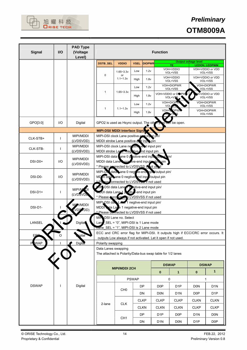
4.1. Pin Definition
Signal I/O PAD Type (Voltage
Level) Function
Global Control Signal
IM[2:0] I Digital
(VDDIO)
Interface mode select pins.
Notes:
(1) Frame buffer writing by MDDI and register reading (or writing) by SPI(or I2C)
could work at the same time.
(2) When MDDI is in stand-by mode, the SPI(or I2C) can also read / write registers
and frame buffer.
(3) MDDI could read / write registers and frame buffer only when SPI (or I2C) is
inactive.
External Pad Set
IM2 IM1 IM0 Interface format
0 0 0 80-series 8-bit MPU interface
0 0 1 80-series 16-bit MPU interface
0 1 0 80-series 24-bit MPU interface
0 1 1 RGB + SPI
1 0 0 RGB + I2C
1 0 1 MIPI-DSI
1 1 0 MDDI + SPI
1 1 1 MDDI + I2C
IM[3] I Digital
(VDDIO)
Input pin to select the SCL rising/falling edge trigger for SPI I/F only. - IM3=”0”, SCL rising edge trigger - IM3=”1”, SCL falling edge trigger
If not used, please connect to VSSI.
RESX I Digital Global Reset Signal. Active Low. If not used please let it floating.
TE_L O Digital Tearing effect output pin to synchronies MCU to frame writing, activated by S/W command. When this pin is not activated (TE function OFF), this pin is VSS level.
TE_R(TE) O Digital Tearing effect output pin to synchronies MCU to frame writing, activated by S/W command. When this pin is not activated (TE function OFF), this pin is VSS level.
LEDPWM O Digital LCD backlight control PWM output pin
LEDON O Digital Enable pulse for the backlight driver
VSEL I Digital
DIOPWR voltage select
“Low” = 1.2V IO mode
“High” = 1.8V IO mode
I2C_SA[1:0] I Digital
Selection of I2C slave address Connect to VSS if not used.
2’b00 : Slave Address=1001100
2’b01 : Slave Address=1001101
2’b10 : Slave Address=1001110
2’b11 : Slave Address=1001111
NBWSEL I Digital Selection for NB(Normally Black)/NW(Normally White) panel. 0 : NW, 1 : NB
DSTB_SEL I Digital Control pin for DIOPWR regulator.
0 : not used , 1 : used for TE/LEDON/LEDPWM.
ORISE Tec
h Con
fiden
tial
For IV
O Use
Only
PPrreelliimmiinnaarryy
OTM8009A
© ORISE Technology Co., Ltd.
Proprietary & Confidential
14 FEB.22, 2012
Preliminary Version 0.8
Signal I/O PAD Type (Voltage
Level) Function
TE LEDON, LEDPWM
Low 1.2vVOH=VDDIO
VOL=VSSVOH=VDDIO or VDD
VOL=VSS
High 1.8vVOH=VDDIO
VOL=VSSVOH=VDDIO or VDD
VOL=VSS
Low 1.2vVOH=DIOPWR
VOL=VSSVOH=DIOPWR
VOL=VSS
High 1.8vVOH=VDDIO or DIOPWR
VOL=VSSVOH=VDDIO or VDD
VOL=VSS
Low 1.2vVOH=DIOPWR
VOL=VSSVOH=DIOPWR
VOL=VSS
High 1.8vVOH=DIOPWR
VOL=VSSVOH=DIOPWR
VOL=VSS
1 1.1~1.3v
01.65~3.3v
or1.1~1.3v
1 1.65~3.3v
DSTB_SEL VDDIO VSEL DIOPWROutput voltage level
GPO[3:0] I/O Digital GPO2 is used as Hsync output. The other pins can be open.
MIPI-DSI/ MDDI Interface Signals
CLK-STB+ I MIPI/MDDI
(LVDSVDD)
MIPI-DSI clock Lane positive-end input pin/
MDDI strobe Lane positive-end input pin
CLK-STB- I MIPI/MDDI
(LVDSVDD)
MIPI-DSI clock Lane negative-end input pin/
MDDI strobe Lane negative-end input pin
DSI-D0+ I/O MIPI/MDDI
(LVDSVDD)
MIPI-DSI data Lane 0 positive-end input/output pin/
MDDI data Lane 0 positive-end input/output pin
* Please connected to LVDSVSS if not used
DSI-D0- I/O MIPI/MDDI
(LVDSVDD)
MIPI-DSI data Lane 0 negtive-end input/output pin/
MDDI data Lane 0 negtive-end input/output pin
* Please connected to LVDSVSS if not used
DSI-D1+ I MIPI/MDDI
(LVDSVDD)
MIPI-DSI data Lane 1 positive-end input pin/
MDDI data Lane 1 positive-end input pin
* Please connected to LVDSVSS if not used
DSI-D1- I MIPI/MDDI
(LVDSVDD)
MIPI-DSI data Lane 1 negtive-end input pin/
MDDI data Lane 1 negative-end input pin
* Please connected to LVDSVSS if not used
LANSEL I Digital
MIPI-DSI Lane no. Select
Lane_SEL = “0”, MIPI-DSI is 1 Lane mode
Lane_SEL = “1”, MIPI-DSI is 2 Lane mode
ERR O Digital ECC and CRC error flag for MIPI-DSI. It outputs high if ECC/CRC error occurs. It
outputs Low always if not activated. Let it open if not used.
PSWAP I Digital Polarity swapping
DSWAP I Digital
Data Lanes swapping
The attached is Polarity/Data-bus swap table for 1/2 lanes
DSWAP DSWAP MIPI/MDDI 2CH
0 1 0 1
PSWAP 0 1
DP D0P D1P D0N D1N CH0
DN D0N D1N D0P D1P
CLKP CLKP CLKP CLKN CLKN CLK
CLKN CLKN CLKN CLKP CLKP
DP D1P D0P D1N D0N
2-lane
CH1 DN D1N D0N D1P D0P
ORISE Tec
h Con
fiden
tial
For IV
O Use
Only

PPrreelliimmiinnaarryy
OTM8009A
© ORISE Technology Co., Ltd.
Proprietary & Confidential
15 FEB.22, 2012
Preliminary Version 0.8
Signal I/O PAD Type (Voltage
Level) Function
DSWAP DSWAP MIPI/MDDI 1CH
0 1 0 1
PSWAP 0 1
DP D0P D0N CH0
DN D0N D0P
CLKP CLKP CLKP CLKN CLKN CLK
CLKN CLKN CLKN CLKP CLKP
DP D0P D0N
1-lane
CH1 DN D0N D0P
MPU/ RGB/ SPI/ I2C Interface
CSX I Digital
(VDDIO)
Chip select signal.
”0” : the OTM8009A is accessible
”1” : the OTM8009A is not accessible
This pin can be permanently fixed “0” in MCU interface mode only.
DCX I Digital
(VDDIO)
Display data / Command selection pin in parallel interface
“0” : Command data
“1” : Display data
Must connect to the VSS or VDDIO level when not used.
WRX/ R_WX/ SCL/
I2C_SCL I
Digital
(VDDIO)
In MPU interface mode, a write strobe signal can be input via this pin and initializes a
write operation when the signal is low.
Must connect to the VSS or VDDIO level when not used.
[Serial-IF] SCL: Serial interface Clock Input
[I2C-IF]I2C_SCL:Serial Clock input
RDX/E I Digital
(VDDIO)
In MPU interface mode, a read strobe signal can be input via this pin and initializes a
read operation when the signal is low.
Must connect to the VSS or VDDIO level when not in use.
D[23:0] I/O Digital
(VDDIO)
MPU/RGB I/F Data Input/Output. If not in use, it can be open or connect them to
ground
DE I Digital
(VDDIO) RGB interface Data Enable Input. If not in use, it can be open or connect it to ground
PCLK I Digital
(VDDIO) RGB interface Picel clock Input. If not in use, it can be open or connect it to ground
HS I Digital
(VDDIO) RGB interface Hsync. Input. If not in use, it can be open or connect it to ground
VS I Digital
(VDDIO) RGB interface Vsync. Input. If not in use, it can be open or connect it to ground
SDI/ I2C_SDA I Digital
(VDDIO)
[Serial-IF]SDI :Serial interface DATA Input
[I2C-IF]I2C_SDA:Serial data input. If not in use, it can be open or connect it to ground
SDO O Digital
(VDDIO) Serial interface DATA output
Source/Panel control and VCOM Signals
S[1440:1] O Analog Output source driver signals. The D/A converted 256-gray-scale analog voltage is
output.
GOUT(GDOUT)
[32:1] O Analog Gate control signals for panel
SDUM0 ~SDUM3 O Analog Source dummy output
ORISE Tec
h Con
fiden
tial
For IV
O Use
Only

PPrreelliimmiinnaarryy
OTM8009A
© ORISE Technology Co., Ltd.
Proprietary & Confidential
16 FEB.22, 2012
Preliminary Version 0.8
Signal I/O PAD Type (Voltage
Level) Function
VCOM O Analog VCOM signal output
Test/ Debugging/ Dummy Pins
PADA[4:1] I/O
For bonding resistance measurement.
There are two groups of pins, they are(1). (PADA1, PADA2). (2). (PADA3, PADA5,
PADA6) and (PADA4, PADA7). The pins in each groups are short together.
PADB[4:1] I/O
For bonding resistance measurement.
There are two groups of pins, they are (1). (PADB1, PADB2) (2). (PADB3, PADB5,
PADB6), and (PADB4, PADB7). The pins in each groups are short together.
TEST[7:0] I/O Test pin. please let them float.
OSC_TEST I/O Test pin. please let them float.
VREFCP Analog Test pin
LVGL[2:1] Analog Test pin
VGSW[3:0] I Digital Test pin
CSP O Analog Dummy pins Hi-Z state
CSN O Analog Dummy pins Hi-Z state
EXTP O Analog Dummy pins Hi-Z state
EXTN O Analog Dummy pins Hi-Z state
CONTACT[2:1]A O Analog Dummy pins Hi-Z state
CONTACT[2:1]B O Analog Dummy pins Hi-Z state
VRGH_DMY O Analog Dummy pins Hi-Z state
VGL_REG1 O Analog Dummy pins Hi-Z state
EXB1T I Digital Dummy Pin
Charge Pump Capacitor
C11P/N,
C12P/N
C13P/N, C14P/N,
C21P/N, C22P/N,
C23P/N, C24P/N,
C31P/N, C32P/N,
C41P/N,
C51P/N
C Step-up
capacitor
Connect boost capacitors for the internal DC/DC converter circuit to these pins.
Leave the pins open when DC/DC converter circuits are not used.
Power Supply and Regulator pins
VCC I Power Supply Power supply to the internal logic power regulator circuit (VCC=2.3 to 4.8V)
VDD(VPNL)
I Power Supply Power Supply input for analog circuit. (VDDA,VDDR,VDD_DET,VDD_R,VDDB)
VDDIO I Power Supply
External Power Supply for Digital Circuits and IO pads.
VDDIO=1.65 to 3.3V
VDDIOL=1.1V to 1.3V
(VDDI_OPT1,VDDI_OPT2,VDDI)
MTP_PWR I Power Supply
- Input power for NV memory programming
- Input power range : 7.25 ~ 7.75V (Typical=7.5V)
- When not under programming, MTP_PWR pin can be float or tied to ground.
VDDAM I Power Supply Power Supply for MIPI/MDDI regulator circuits.(VDDAM=2.3 to 4.8V)
VSSA I Ground Analog Ground (AVSS)
VSS I Ground Digital Ground (VSSIDUM[3:0],VSSR,DVSS,VSSI,VSSB)
LVDSVSS I Ground MIPI/ MDDI Ground (VSSAM)
VDD_18V O Analog Output
Internal Power Supply for Digital Logic Circuits.
Connect to a stabilizing capacitor. VDD_18V=1.5V
(DVDD)
LVDSVDD O Analog Output Internal Power Supply for MIPI/ MDDI. Connect to a stabilizing capacitor. (MVDDA)
ORISE Tec
h Con
fiden
tial
For IV
O Use
Only

PPrreelliimmiinnaarryy
OTM8009A
© ORISE Technology Co., Ltd.
Proprietary & Confidential
17 FEB.22, 2012
Preliminary Version 0.8
Signal I/O PAD Type (Voltage
Level) Function
VDDP O Analog Output LDO output for MIPI YX use(LPDT). VDDP=1.2V(Typical) (MVDDL)
VREF O Analog Output Reference Voltage Connect to a stabilizing capacitor. VREF=2.0V
(VREF_PWR)
DIOPWR O Analog Output
Internal voltage regulator output for Dual I/O. DIOPWR=1.8V or 1.2V
Must connect a capacitor for stabilizing .
Please refer to VSEL pin description.
- Let it open if Dual I/O are NOT used
Charge Pump/ Booster / Regulator Related pins
VDDA O Analog
Positive Output voltage from the step-up circuit
Connect to a stabilizing capacitor. (AVDD)
NVDDA O Analog
Negative Output voltage from the step-up circuit
Connect to a stabilizing capacitor.
(AVEE)
VGH O Analog Positive Output voltage from the step-up circuit
VGHO_L
VGHO_R O Analog Positive Power supply to gate control signal and circuit in Panel (VGHO)
VRGH O Analog Regulator output voltage generated from VGH
Connect with a stabilizing capacitor.
VGL O Analog Negative Output voltage from the step-up circuit (VGLO,VGLX)
VGL_REG O Analog Regulator output voltage generated from VGL
Connect with a stabilizing capacitor.
VGMP O Analog Output voltage generated from from VDDA. It’s used for positive gamma voltage.
VGMP is applied for GVDD test pin.
VGMN O Analog Output voltage generated from from NVDDA. It’s used for negative gamam voltage.
VGMN is applied for NGVDD test pin.
VGSP O Analog Dummy Pin
VGSN O Analog Dummy Pin
VCL O Analog Output voltage from the step-up circuit
ORISE Tec
h Con
fiden
tial
For IV
O Use
Only

PPrreelliimmiinnaarryy
OTM8009A
© ORISE Technology Co., Ltd.
Proprietary & Confidential
18 FEB.22, 2012
Preliminary Version 0.8
4.2. Power Architecture
VGL
VSS(optional)
VCOMVCOM
VDD
VCL
VGMP
GVDD/NGVDDRegulator
VGMP
VGMNVGMN
VDDA
NVDDA
VCL
Gamma
(to Source)
VSDP[255:0]
VSDN[255:0]
VDDA
NVDDA
VRGHRegulator
VGH VRGH
(optional)
VGL_REGRegulator
VGL VGL_REG
(optional)
VDD_18V Regulator
VCC VDD_18VVREF
RegulatorVDD VREF
LVDSVDD Regulator
VDDAM LVDSVDD
(to MIPI/MDDI)
VDDP Regulator
VDDAM VDDP
(to MIPI/MDDI)
DIOPWRRegulator
VPNL DIOPWR-1.0XVDDA
VDDIO VDD
VDDA PUMP
VDD 1.0xVDD1.5xVDD2.0xVDD3.0xVDDC11P
C11N
C12P
C12N
C13P
C13N
C14P
C14N
VDDA
NVDDA PUMP
VDDA
C21P
C21N
C22P
C22N
C23P
C23N
C24P
C24N
NVDDA
C31P
C31N
VDD
VCL PUMP
-1.0xVDD
VCLC32P
C32N
Source Driver
(to Panel)
VSDP[255:0]
VSDN[255:0]
S[1440:1]
SDUM[3:0](optional)
VGH &VGL PUMP
VDDA
NVDDA
VGH :2xVDDA- NVDDA3xVDDA- NVDDA
VGL:- NVDDA - VDDA
- 2xNVDDA - VDDA
C41P
C41N
C51P
C51N
VGH
VGL
ORISE Tec
h Con
fiden
tial
For IV
O Use
Only
PPrreelliimmiinnaarryy
OTM8009A
© ORISE Technology Co., Ltd.
Proprietary & Confidential
19 FEB.22, 2012
Preliminary Version 0.8
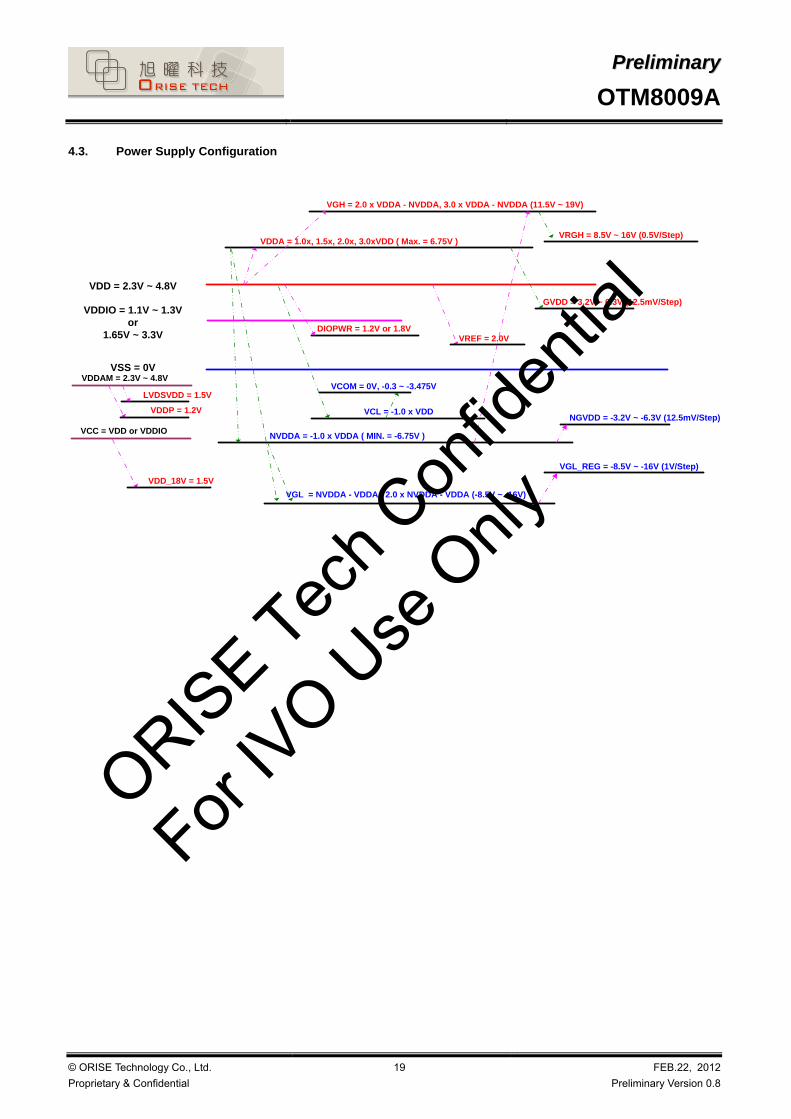
4.3. Power Supply Configuration
VDD = 2.3V ~ 4.8V
VSS = 0V
VGH = 2.0 x VDDA - NVDDA, 3.0 x VDDA - NVDDA (11.5V ~ 19V)
NVDDA = -1.0 x VDDA ( MIN. = -6.75V )
VDDIO = 1.1V ~ 1.3V or
1.65V ~ 3.3V
VCL = -1.0 x VDD
VREF = 2.0VDIOPWR = 1.2V or 1.8V
VDDA = 1.0x, 1.5x, 2.0x, 3.0xVDD ( Max. = 6.75V )
VCOM = 0V, -0.3 ~ -3.475VLVDSVDD = 1.5V
VDDAM = 2.3V ~ 4.8V
VDDP = 1.2V
VGL = NVDDA - VDDA, 2.0 x NVDDA - VDDA (-8.5V ~ -16V)
GVDD = 3.2V ~ 6.3V (12.5mV/Step)
NGVDD = -3.2V ~ -6.3V (12.5mV/Step)
VRGH = 8.5V ~ 16V (0.5V/Step)
VGL_REG = -8.5V ~ -16V (1V/Step)
VDD_18V = 1.5V
VCC = VDD or VDDIO
ORISE Tec
h Con
fiden
tial
For IV
O Use
Only

PPrreelliimmiinnaarryy
OTM8009A
© ORISE Technology Co., Ltd.
Proprietary & Confidential
20 FEB.22, 2012
Preliminary Version 0.8
4.4. BOM List
OTM8009A BOM LISTS
NO. Signal Name Value Max. Ability Note
1 VDDIO 1.0uF 4V I/O and Digtal Power
2 VDD 2.2uF 6.3V Analog Power
3 C11P/C11N 1.0~2.2 uF 6.3V
4 C12P/C12N 1.0~2.2 uF 6.3V
5 C13P/C13N 1.0~2.2 uF 6.3V
6 C14P/C14N 1.0~2.2 uF 6.3V
7 VDDA 2.2uF 10V
VDDA Pump
8 C21P/C21N 1.0~2.2 uF 6.3V
9 C22P/C22N 1.0~2.2 uF 6.3V
10 C23P/C23N 1.0~2.2 uF 6.3V
11 C24P/C24N 1.0~2.2 uF 6.3V
12 NVDDA 2.2uF 10V
NVDDA Pump
13 C31P/31N 1.0~2.2 uF 6.3V
14 C32P/C32N 1.0~2.2 uF 6.3V
15 VCL 2.2uF 6.3V
VCL Pump
16 C41P/C41N 1.0uF 16V
17 VGH 1.0uF 25V VGH Pump
18 C51P/C51N 1.0uF 16V
19 VGL 1.0uF 20v VGL Pump
20 VREF 1.0uF 4V Regulator
21 VCOM 2.2uF 4V VCOM
22 VDD_18V 2.2uF 4V TCON Power
23 DIOPWR 1.0uF 4V BC, TE, RESX Power
24 LVDSVDD 1.0uF 4V
25 VDDP 1.0uF 4V Mipi, RX, DSI Power
26 VGL Schottky Diode Optional
27 VRGH 1.0uF 20V Optional
28 VGL_REG 1.0uF 20V Optional
Note: Gray words is optional and removable.
ORISE Tec
h Con
fiden
tial
For IV
O Use
Only

PPrreelliimmiinnaarryy
OTM8009A
© ORISE Technology Co., Ltd.
Proprietary & Confidential
21 FEB.22, 2012
Preliminary Version 0.8
5. INSTRUCTIONS
5.1. Outline
The OTM8009A supports high speed serial interface, MIPI, MDDI, to configure system via accessing command register. When the
command register is executed, sending the command information to specify which index register would be accessed and following the data
to that control register. The MIPI-DSI is compliant with MIPI Alliance Standard for Display Serial Interface(DSI), Version 1.01.00 and D-PHY
Version 1.00.00. And command instruction can be accomplished using all supporting system interfaces (MIPI, and I-80 24-bit parallel bus
interface).
The OTM8009A has the following major categories of instructions:
(1) System function instructions (User Command Set).
(2) Customer Command List and Description (Manufacturer Command Set / Command 2).
These instructions are asyncrounous to the OTM8009A internal clock, requiring no wait cycles. Because the writing of instruction data
does not interfere with the host controller processing, instructions can be handles smoothly and effiencently. The following describes details
of instruction settings.
ORISE Tec
h Con
fiden
tial
For IV
O Use
Only

PPrreelliimmiinnaarryy
OTM8009A
© ORISE Technology Co., Ltd.
Proprietary & Confidential
22 FEB.22, 2012
Preliminary Version 0.8
5.1.1. System function command list and description
Table 5.1 list all the system function command. After the H/W reset by RESX pin or S/W reset by SWRESET command, each internal
register becomes default state (Refer “RESET TABLE” section). Commands 10h, 12h, 13h, 20h, 21h, 26h, 28h, 29h, 30h, 33h, 36h (ML
parameter only), 38h, and 39h are updated during V-sync when Module is in Sleep Out Mode to avoid abnormal visual effects. During Sleep
In mode, these commands are updated immediately. Read Display Power Mode (0Ah), Read Display MADCTR (0Bh), Read Display Pixel
Format (0Ch), Read Display Image Mode (0Dh), Read Display Signal Mode (0Eh), and Read Display Self Diagnostic Result (0Fh) of these
commands are updated immediately both in Sleep In mode and Sleep Out mode.
Table 5-1 System Function command list
Command (Hex) Write/Read/Command Function Parameter
Number MIPI Transmissiom
Mode NOP 00 C No Operation 0 LPDT/HSDT
SWRESET 01 C Software reset 0 LPDT/HSDT
RDNUMED 05 R Read Number of the Errors on DSI 1 LPDT/HSDT
RDDPM 0A R Read Display Power Mode 1 LPDT/HSDT
RDDMADCTL 0B R Read Display MADCTL 1 LPDT/HSDT
RDDCOLMOD 0C R Read Display Pixel Format 1 LPDT/HSDT
RDDIM 0D R Read Display Image Mode 1 LPDT/HSDT
RDDSM 0E R Read Display Signal Mode 1 LPDT/HSDT
RDDSDR 0F R Read Display Self Diagnostic Result 1 LPDT/HSDT
SLPIN 10 C Sleep in 0 LPDT/HSDT
SLPOUT 11 C Sleep out 0 LPDT/HSDT
PTLON 12 C Partial Mode On 0 LPDT/HSDT
NORON 13 C Normal Display Mode On 0 LPDT/HSDT
INVOFF 20 C Display Inversion Off 0 LPDT/HSDT
INVON 21 C Display Inversion On 0 LPDT/HSDT
ALLPOFF 22 C All Pixels Off 0 LPDT/HSDT
ALLPON 23 C All Pixels On 0 LPDT/HSDT
GAMSET 26 W Gamma Set 1 LPDT/HSDT
DISPOFF 28 C Display off 0 LPDT/HSDT
DISPON 29 C Display on 0 LPDT/HSDT
CASET 2A W Column Address Set 4 LPDT/HSDT
PASET 2B W Page Address Set 4 LPDT/HSDT
RAMWR 2C W Memory Write Any Length LPDT/HSDT
RAMRD 2E R Memory Read Any Length LPDT/HSDT
PLTAR 30 W Partial area 4 LPDT/HSDT
TEOFF 34 C Tearing Effect Line Off 0 LPDT/HSDT
TEEON 35 W Tearing Effect Line On 1 LPDT/HSDT
MADCTL 36 W Memory Access Control 1 LPDT/HSDT
IDMOFF 38 C Idle Mode off 0 LPDT/HSDT
IDMON 39 C Idle Mode on 0 LPDT/HSDT
COLMOD 3A C Interface Pixel Format 1 LPDT/HSDT
RAMWRC 3C W Memory Write Continue Any Length LPDT/HSDT
RAMRDC 3E R Memory Read Continue Any Length LPDT/HSDT
WRTESCN 44 W Write TE Scan Line 2 LPDT/HSDT
RDSCNL 45 R Read Scan Line 2 LPDT/HSDT
WRDISBV 51 W Write Display Brightness 1 LPDT/HSDT
RDDISBV 52 R Read Display Brightness Value 1 LPDT/HSDT
WRCTRLD 53 W Write CTRL Display 1 LPDT/HSDT
RDCTRLD 54 R Read CTRL Display 1 LPDT/HSDT
WRCABC 55 W Write Content Adaptive Brightness Control 1 LPDT/HSDT
RDCABC 56 R Read Content Adaptive Brightness Control 1 LPDT/HSDT
WRCABCMB 5E W Write CABC Minimum Brightness 1 LPDT/HSDT
RDCABCMB 5F R Read CABC Minimum Brightness 1 LPDT/HSDT
RDABCSDR 68 R Read Automatic Brightness Control Self-diagnostics Result 1 LPDT/HSDT
RDBWLB 70 R Read Black/White Low Bits 1 LPDT/HSDT
ORISE Tec
h Con
fiden
tial
For IV
O Use
Only

PPrreelliimmiinnaarryy
OTM8009A
© ORISE Technology Co., Ltd.
Proprietary & Confidential
23 FEB.22, 2012
Preliminary Version 0.8
RDBKx 71 R Read Bkx 1 LPDT/HSDT
RDBKy 72 R Read Bky 1 LPDT/HSDT
RDWx 73 R Read Wx 1 LPDT/HSDT
RDWy 74 R Read Wy 1 LPDT/HSDT
RDRGLB 75 R Read Red/Green Low Bits 1 LPDT/HSDT
RDRx 76 R Read Rx 1 LPDT/HSDT
RDRy 77 R Read Ry 1 LPDT/HSDT
RDGx 78 R Read Gx 1 LPDT/HSDT
RDGy 79 R Read Gy 1 LPDT/HSDT
RDBALB 7A R Read Blue/AColour Low Bits 1 LPDT/HSDT
RDBx 7B R Read Bx 1 LPDT/HSDT
RDBy 7C R Read By 1 LPDT/HSDT
RDAx 7D R Read Ax 1 LPDT/HSDT
RDAy 7E R Read Ay 1 LPDT/HSDT
RDDDBS A1 R Read DDB Start 5 LPDT/HSDT
RDDDBC A8 R Read DDB Continue Any Length LPDT/HSDT
RDFCS AA R Read First Checksum 1 LPDT/HSDT
RDCCS AF R Read Continue Checksum 1 LPDT/HSDT
RDID1 DA R Read ID1 1 LPDT/HSDT
RDID2 DB R Read ID2 1 LPDT/HSDT
RDID3 DC R Read ID3 1 LPDT/HSDT
Note:LPDT (Low Power Mode), HSDT (High Speed Mode)
ORISE Tec
h Con
fiden
tial
For IV
O Use
Only

PPrreelliimmiinnaarryy
OTM8009A
© ORISE Technology Co., Ltd.
Proprietary & Confidential
24 FEB.22, 2012
Preliminary Version 0.8
Table 5-2 command2 list
Command (Hex) Write/Read /Command
Function Parameter
Number MIPI Transmissiom
Mode
ADRSFT 0000 W Address Shift Function 1 LPDT
CMD2_ENA1 FF00 W Enable Access Command2 “CMD2” 3 LPDT
CMD2_ENA2 FF80 W Enable Access Orise Command2 2 LPDT
OTPSEL A000 W/R OTP Select Region 1 LPDT
MIPISET1 B080 W/R MIPI Setting1 4 LPDT
MIPISET2 B0A1 W/R MIPI Setting2 5 LPDT
IF_PARA1 B280 W/R IF Parameter 1 1 LPDT
IF_PARA2 B282 W/R IF Parameter 2 1 LPDT
PAD_PARA B390 W/R IOPAD Parameter 3 LPDT
RAMPWRSET B3C0 W/R SRAM Power Setting 2 LPDT
TSP1 C080 W/R TCON Setting Parameter1 9 LPDT
PTSP1 C092 W/R Panel Timing Setting Parameter1 2 LPDT
PTSP2 C094 W/R Panel Timing Setting Parameter2 1 LPDT
SD_CTRL C0A2 W/R Source Driver Timing Setting 6 LPDT
P_DRV_M C0B4 W/R Panel Driving Mode 1 LPDT
OSC_ADJ C181 W/R Oscillator Adjustment for Idle/Normal Mode 1 LPDT
RGB_VIDEO_SET C1A1 W/R RGB Video Mode Setting 1 LPDT
SD_PCH_CTRL C480 W/R Source Driver Precharge Control 9 LPDT
PWR_CTRL1 C580 W/R Power Control Setting 1 4 LPDT
PWR_CTRL2 C590 W/R Power Control Setting 2 for Normal Mode 7 LPDT
PWR_CTRL3 C5A0 W/R Power Control Setting 3 for Idle Mode 7 LPDT
PWR_CTRL4 C5B0 W/R Power Control Setting 4 for DC Voltage Settings 2 LPDT
PWM_PARA1 C680 W/R PWM_PARA1 (C680H) PWM Parameter 1 1 LPDT
PWM_PARA2 C6B0 W/R PWM_PARA2 (C6B0H) PWM Parameter 2 1 LPDT
PWM_PARA3 C6B1 W/R PWM_PARA3 (C6B1H) PWM Parameter 3 1 LPDT
PWM_PARA4 C6B2 W/R PWM_PARA4 (C6B3H) PWM Parameter 4 1 LPDT
PWM_PARA5 C6B3 W/R PWM_PARA5 (C6B4H) PWM Parameter 5 1 LPDT
PWM_PARA6 C6B4 W/R PWM_PARA6 (C6B5H) PWM Parameter 6 1 LPDT
CABCSET1 C700 W/R CABC Setting 1 LPDT
CABCSET2 C800 W/R CABC Gamma Curve Setting 18 LPDT
AIESET C900 W/R AIE Setting 18 LPDT
GOAVST CE80 W/R GOA VST Setting 12 LPDT
GOAVEND CE90 W/R GOA VEND Setting 12 LPDT
GOAGPSET CE9C W/R GOA Group Setting 2 LPDT
GOACLKA1 CEA0 W/R GOA CLKA1 Setting 7 LPDT
GOACLKA2 CEA7 W/R GOA CLKA2 Setting 7 LPDT
GOACLKA3 CEB0 W/R GOA CLKA3 Setting 7 LPDT
GOACLKA4 CEB7 W/R GOA CLKA4 Setting 7 LPDT
GOACLKB1 CEC0 W/R GOA CLKB1 Setting 7 LPDT
GOACLKB2 CEC7 W/R GOA CLKB2 Setting 7 LPDT
GOACLKB3 CED0 W/R GOA CLKB3 Setting 7 LPDT
GOACLKB4 CED7 W/R GOA CLKB4 Setting 7 LPDT
GOACLKC1 CF80 W/R GOA CLKC1 Setting 7 LPDT
GOACLKC2 CF87 W/R GOA CLKC2 Setting 7 LPDT
GOACLKC3 CF90 W/R GOA CLKC3 Setting 7 LPDT
GOACLKC4 CF97 W/R GOA CLKC4 Setting 7 LPDT
GOACLKD1 CFA0 W/R GOA CLKD1 Setting 7 LPDT
GOACLKD2 CFA7 W/R GOA CLKD2 Setting 7 LPDT
GOACLKD3 CFB0 W/R GOA CLKD3 Setting 7 LPDT
GOACLKD4 CFB7 W/R GOA CLKD4 Setting 7 LPDT
GOAECLK CFC0 W/R GOA ECLK Setting 6 LPDT
ORISE Tec
h Con
fiden
tial
For IV
O Use
Only

PPrreelliimmiinnaarryy
OTM8009A
© ORISE Technology Co., Ltd.
Proprietary & Confidential
25 FEB.22, 2012
Preliminary Version 0.8
GOAOPT1 CFC6 W/R GOA Other Options 1 1 LPDT
GOATGOPT CFC7 W/R GOA Signal Toggle Option Setting 3 LPDT
WRID1 D000 W/R ID1 Setting 1 LPDT
WRID2 D100 W/R ID2/ID3 Setting 2 LPDT
WRDDB D200 W/R DDB Setting 4 LPDT
EXTCCHK D300 R EXTC Check 1 LPDT
CESET1 D400 W/R CE Correction Characteristics Setting1 360 LPDT
CESET2 D500 W/R CE Correction Characteristics Setting2 360 LPDT
CEEN D680 W/R CE Enable 1 LPDT
AIEEN D700 W/R AIE Enable 1 LPDT
GVDDSET D800 W/R GVDD/NGVDD Setting 2 LPDT
VCOMDC D900 W/R VCOM Voltage Setting 1 LPDT
GMCT22P E100 W/R Gamma Correction Characteristics Setting (2.2 + ) 16 LPDT
GMCT22N E200 W/R Gamma Correction Characteristics Setting (2.2 - ) 16 LPDT
GMCT18P E300 W/R Gamma Correction Characteristics Setting (1.8 + ) 16 LPDT
GMCT18N E400 W/R Gamma Correction Characteristics Setting (1.8 - ) 16 LPDT
GMCT25P E500 W/R Gamma Correction Characteristics Setting (2.5 + ) 16 LPDT
GMCT25N E600 W/R Gamma Correction Characteristics Setting (2.5 - ) 16 LPDT
GMCT10P E700 W/R Gamma Correction Characteristics Setting (1.0 + ) 16 LPDT
GMCT10N E800 W/R Gamma Correction Characteristics Setting (1.0 - ) 16 LPDT
NVMIN EB00 W NV Memory Write Mode 1 LPDT
DGAMR EC00 W/R Digital Gamma Correction Characteristics Setting (Red) 17 LPDT
DGAMG ED00 W/R Digital Gamma Correction Characteristics Setting (Green) 17 LPDT
DGAMB EE00 W/R Digital Gamma Correction Characteristics Setting (Blue) 17 LPDT
PRG_FLAG F101 R OTP Program flag Check 3 LPDT
Note:LPDT (Low Power Mode), HSDT (High Speed Mode)
ORISE Tec
h Con
fiden
tial
For IV
O Use
Only

PPrreelliimmiinnaarryy
OTM8009A
© ORISE Technology Co., Ltd.
Proprietary & Confidential
26 FEB.22, 2012
Preliminary Version 0.8
5.2. System Command Description
5.2.1. NOP (00h): No Operation
Address (MIPI) 00h
(MDDI/SPI) 0x0000
Inst / Para Write/Read D7 D6 D5 D4 D3 D2 D1 D0 (Code)
NOP Write
0 0 0 0 0 0 0 0 (00H)
Parameter No Parameter -
NOTE: “-” Don’t care, can be set to VDDIO or VSS level
Description - This command is empty command. It does not have effect on the display module.
- However it can be used to terminate RAM data write or read as described in RAMWR (Memory Write), RAMRD (Memory Read) and parameter write commands.
Restriction -
Register Availability
Status Availability
Normal Mode On, Idle Mode Off, Sleep Out Yes Normal Mode On, Idle Mode On, Sleep Out Yes Partial Mode On, Idle Mode Off, Sleep Out Yes Partial Mode On, Idle Mode On, Sleep Out Yes
Sleep In Yes
Default
Status Default Value
Power On Sequence N/A S/W Reset N/A H/W Reset N/A
ORISE Tec
h Con
fiden
tial
For IV
O Use
Only

PPrreelliimmiinnaarryy
OTM8009A
© ORISE Technology Co., Ltd.
Proprietary & Confidential
27 FEB.22, 2012
Preliminary Version 0.8
5.2.2. SWRESET (01h): Software Reset
Address (MIPI) 01h
(MDDI/SPI) 0x0100
Inst / Para Write/Read D7 D6 D5 D4 D3 D2 D1 D0 (Code)
SWRESET Write
0 0 0 0 0 0 0 1 (01H)
Parameter No Parameter -
NOTE: “-” Don’t care, can be set to VDDIO or VSS level
Description
- When the Software Reset command is written, it causes a software reset. It resets the commands and parameters to their S/W Reset default values and all source & gate outputs are set to VSS (display off). (See default tables in each command description)
Note: The Frame Memory contents are not affected by this command.
Restriction
- It will be necessary to wait 5msec before sending new command following software reset.
-The display module loads all display supplier’s factory default values to the registers during 5msec.
- If Software Reset is applied during Sleep Out mode, it will be necessary to wait 120msec before sending Sleep Out command.
-Software Reset command cannot be sent during Sleep Out sequence.
Register Availability
Status Availability
Normal Mode On, Idle Mode Off, Sleep Out Yes Normal Mode On, Idle Mode On, Sleep Out Yes Partial Mode On, Idle Mode Off, Sleep Out Yes Partial Mode On, Idle Mode On, Sleep Out Yes
Sleep In Yes
Default
Status Default Value
Power On Sequence N/A S/W Reset N/A H/W Reset N/A
ORISE Tec
h Con
fiden
tial
For IV
O Use
Only

PPrreelliimmiinnaarryy
OTM8009A
© ORISE Technology Co., Ltd.
Proprietary & Confidential
28 FEB.22, 2012
Preliminary Version 0.8
5.2.3. RDNUMED (05H) Read Number of the Errors on DSI
Address (MIPI) 05h
(MDDI/SPI) 0x0500
Inst / Para Write/Read D7 D6 D5 D4 D3 D2 D1 D0 (Code)
RDNUMED Write 0 0 0 0 0 1 0 1 (05H)
1st Parameter Read
P7 P6 P5 P4 P3 P2 P1 P0 -
NOTE: “-” Don’t care, can be set to VDDIO or VSS level
Description
- The first parameter is telling a number of the errors on DSI. The more detailed description of the bits is below.
- P[6.. 0] bits are telling a number of the errors.
- P[7] is set to ‘1’ if there is overflow with P[6..0] bits.
- P[7..0] bits are set to ‘0’s (as well as RDDSM(0EH)’s D0 is set ‘0’ at the same time) after there is sent the second parameter information (= The read function is completed).
- See Read Display Signal Mode (0EH)”.
Restriction
Register Availability
Status Availability
Normal Mode On, Idle Mode Off, Sleep Out Yes Normal Mode On, Idle Mode On, Sleep Out Yes Partial Mode On, Idle Mode Off, Sleep Out Yes Partial Mode On, Idle Mode On, Sleep Out Yes
Sleep In Yes
Default
Status Default Value
Power On Sequence 00h S/W Reset 00h H/W Reset 00h
ORISE Tec
h Con
fiden
tial
For IV
O Use
Only

PPrreelliimmiinnaarryy
OTM8009A
© ORISE Technology Co., Ltd.
Proprietary & Confidential
29 FEB.22, 2012
Preliminary Version 0.8
5.2.4. RDDPM (0AH): Read Display Power Mode
Address (MIPI) 0Ah
(MDDI/SPI) 0x0A00
Inst / Para Write/Read D7 D6 D5 D4 D3 D2 D1 D0 (Code)
RDDPM Write 0 0 0 0 1 0 1 0 (0AH)
1st Parameter Read
BSTON IDMON PTLONSLPOUT
NORON
DISON D1 D0 08h
NOTE: “-” Don’t care, can be set to VDDIO or VSS level
Description
-This command indicates the current status of the display as described in the table below:
Bit Description Value
BSTON Booster Voltage Status “1”=Booster on, “0”=Booster off
IDMON Idle Mode On/Off “1” = Idle Mode On, “0” = Idle Mode Off
PTLON Partial Mode On/Off “1” = Partial Mode On, “0” = Partial Mode Off
SLPON Sleep In/Out “1” = Sleep Out, “0” = Sleep In
NORON Display Normal Mode On/Off“1” = Normal Display, “0” = Partial Display
DISON Display On/Off “1” = Display On, “0” = Display Off
D1 Not Used “0” D0 Not Used “0”
Restriction -
Register Availability
Status Availability
Normal Mode On, Idle Mode Off, Sleep Out Yes Normal Mode On, Idle Mode On, Sleep Out Yes Partial Mode On, Idle Mode Off, Sleep Out Yes Partial Mode On, Idle Mode On, Sleep Out Yes
Sleep In Yes
Default
Status Default Value (D7 to D0)
Power On Sequence 08h S/W Reset 08h H/W Reset 08h
ORISE Tec
h Con
fiden
tial
For IV
O Use
Only
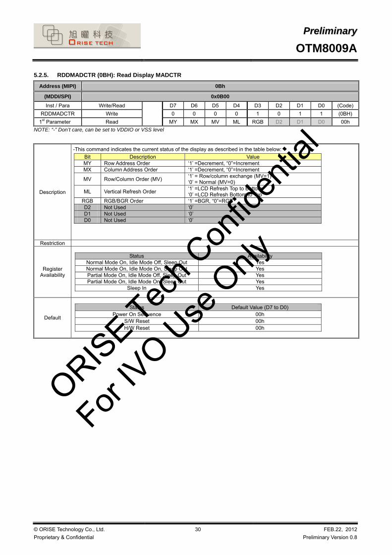
PPrreelliimmiinnaarryy
OTM8009A
© ORISE Technology Co., Ltd.
Proprietary & Confidential
30 FEB.22, 2012
Preliminary Version 0.8
5.2.5. RDDMADCTR (0BH): Read Display MADCTR
Address (MIPI) 0Bh
(MDDI/SPI) 0x0B00
Inst / Para Write/Read D7 D6 D5 D4 D3 D2 D1 D0 (Code)
RDDMADCTR Write 0 0 0 0 1 0 1 1 (0BH)
1st Parameter Read
MY MX MV ML RGB D2 D1 D0 00h
NOTE: “-” Don’t care, can be set to VDDIO or VSS level
Description
-This command indicates the current status of the display as described in the table below:
Bit Description Value MY Row Address Order ‘1’ =Decrement, “0”=Increment MX Column Address Order ‘1’ =Decrement, “0”=Increment
MV Row/Column Order (MV) ‘1’ = Row/column exchange (MV=1) ‘0’ = Normal (MV=0)
ML Vertical Refresh Order ‘1’ =LCD Refresh Top to Bottom ‘0’ =LCD Refresh Bottom to Top
RGB RGB/BGR Order ‘1’ =BGR, “0”=RGB D2 Not Used ‘0’ D1 Not Used ‘0’ D0 Not Used ‘0’
Restriction
Register Availability
Status Availability
Normal Mode On, Idle Mode Off, Sleep Out Yes Normal Mode On, Idle Mode On, Sleep Out Yes Partial Mode On, Idle Mode Off, Sleep Out Yes Partial Mode On, Idle Mode On, Sleep Out Yes
Sleep In Yes
Default
Status Default Value (D7 to D0)
Power On Sequence 00h S/W Reset 00h H/W Reset 00h
ORISE Tec
h Con
fiden
tial
For IV
O Use
Only

PPrreelliimmiinnaarryy
OTM8009A
© ORISE Technology Co., Ltd.
Proprietary & Confidential
31 FEB.22, 2012
Preliminary Version 0.8
5.2.6. RDDCOLMOD (0CH): Read Display Pixel Format
Address (MIPI) 0Ch
(MDDI/SPI) 0x0C00
Inst / Para Write/Read D7 D6 D5 D4 D3 D2 D1 D0 (Code)
RDDCOLMOD Write 0 0 0 0 1 1 0 0 (0CH)
1st Parameter Read
0 0 0 0 0 IFPF2 IFPF1 IFPF0 07h
NOTE: “-” Don’t care, can be set to VDDIO or VSS level
Description
-This command indicates the current status of the display as described in the table below:
IFPF[2:0] MCU Interface Color Format 011 3 12-bits/pixel 101 5 16-bits/pixel 110 6 18-bits/pixel 111 7 24-bits/pixel
Others are no define and invalid
Restriction
Register Availability
Status Availability
Normal Mode On, Idle Mode Off, Sleep Out Yes Normal Mode On, Idle Mode On, Sleep Out Yes Partial Mode On, Idle Mode Off, Sleep Out Yes Partial Mode On, Idle Mode On, Sleep Out Yes
Sleep In Yes
Default
Status Default Value
IFPF[2:0] Power On Sequence 111 (24-bits/pixel)
S/W Reset 111 (24-bits/pixel) H/W Reset 111 (24-bits/pixel)
ORISE Tec
h Con
fiden
tial
For IV
O Use
Only

PPrreelliimmiinnaarryy
OTM8009A
© ORISE Technology Co., Ltd.
Proprietary & Confidential
32 FEB.22, 2012
Preliminary Version 0.8
5.2.7. RDDIM (0DH): Read Display Image Mode
Address (MIPI) 0Dh
(MDDI/SPI) 0x0D00
Inst / Para Write/Read D7 D6 D5 D4 D3 D2 D1 D0 (Code)
RDDIM Write 0 0 0 0 1 1 0 1 (0DH)
1st Parameter Read
D7 D6 INVONALLPX
ON ALLPX
OFFGCS2 GCS1 GCS0 00h
NOTE: “-” Don’t care, can be set to VDDIO or VSS level
Description
-This command indicates the current status of the display as described in the table below:
Bit Description Value D7 Not used D6 For Future Use “0” (Not used)
INVON Inversion On/Off “1” = Inversion is On, “0” = Inversion is Off
ALLPXON All Pixel On “1” = All pixel on is On “0” = All pixel on is Off
ALLPXOFF All Pixel Off “1” = All pixel off is On “0” = All pixel off is Off
GCS2 GCS1
GCS0 Gamma Curve Selection
“000” = GC0, “001” = GC1, “010” = GC2, “011” = GC3, ”100” to “111” = Not defined
Restriction -
Register Availability
Status Availability
Normal Mode On, Idle Mode Off, Sleep Out Yes Normal Mode On, Idle Mode On, Sleep Out Yes Partial Mode On, Idle Mode Off, Sleep Out Yes Partial Mode On, Idle Mode On, Sleep Out Yes
Sleep In Yes
Default
Status Default Value (D7 to D0)
Power On Sequence 00h S/W Reset 00h H/W Reset 00h
ORISE Tec
h Con
fiden
tial
For IV
O Use
Only

PPrreelliimmiinnaarryy
OTM8009A
© ORISE Technology Co., Ltd.
Proprietary & Confidential
33 FEB.22, 2012
Preliminary Version 0.8
5.2.8. RDDSM (0EH): Read Display Signal Mode
Address (MIPI) 0Eh
(MDDI/SPI) 0x0E00
Inst / Para Write/Read D7 D6 D5 D4 D3 D2 D1 D0 (Code)
RDDSM Write 0 0 0 0 1 1 1 0 (0EH)
1st Parameter Read
TEON TELOM D5 D4 D3 D2 D1 D0 00h
NOTE: “-” Don’t care, can be set to VDDIO or VSS level
Description
-This command indicates the current status of the display as described in the table below:
Bit Description Value
TEON Tearing Effect Line On/Off “1” = On, “0” = Off
TELOM Tearing effect line mode “0” = mode1, “1” = mode2
D5 Not Used
D4 Not Used
D3 Not Used
D2 Not Used
D1 Not Used
D0 Not Used
Restriction
Register Availability
Status Availability
Normal Mode On, Idle Mode Off, Sleep Out Yes Normal Mode On, Idle Mode On, Sleep Out Yes Partial Mode On, Idle Mode Off, Sleep Out Yes Partial Mode On, Idle Mode On, Sleep Out Yes
Sleep In Yes
Default
Status Default Value (D7 to D0)
Power On Sequence 00h S/W Reset 00h H/W Reset 00h
ORISE Tec
h Con
fiden
tial
For IV
O Use
Only

PPrreelliimmiinnaarryy
OTM8009A
© ORISE Technology Co., Ltd.
Proprietary & Confidential
34 FEB.22, 2012
Preliminary Version 0.8
5.2.9. RDDSDR (0FH): Read Display Self-Diagnostic Result
Address (MIPI) 0Fh
(MDDI/SPI) 0x0F00
Inst / Para Write/Read D7 D6 D5 D4 D3 D2 D1 D0 (Code)
RDDSDR Write 0 0 0 0 1 1 1 1 (0FH)
1st Parameter Read
RELD FUND D5 D4 D3 D2 D1 D0 00h
NOTE: “-” Don’t care, can be set to VDDIO or VSS level
Description
-This command indicates the current status of the display as described in the table below:
Bit Description Value
RELD Register Loading Detection See section 6.8.1
FUND Functionality Detection See section 6.8.2
D5 Not Used “0”
D4 Not Used “0”
D3 Not Used “0”
D2 Not Used “0”
D1 Not Used “0”
D0 Not Used “0”
Restriction
Register Availability
Status Availability
Normal Mode On, Idle Mode Off, Sleep Out Yes Normal Mode On, Idle Mode On, Sleep Out Yes Partial Mode On, Idle Mode Off, Sleep Out Yes Partial Mode On, Idle Mode On, Sleep Out Yes
Sleep In Yes
Default
Status Default Value (D7 to D0)
Power On Sequence 00h S/W Reset 00h H/W Reset 00h
ORISE Tec
h Con
fiden
tial
For IV
O Use
Only

PPrreelliimmiinnaarryy
OTM8009A
© ORISE Technology Co., Ltd.
Proprietary & Confidential
35 FEB.22, 2012
Preliminary Version 0.8
5.2.10. SLPIN (10H): Sleep In
Address (MIPI) 10h
(MDDI/SPI) 0x1000
Inst / Para Write/Read D7 D6 D5 D4 D3 D2 D1 D0 (Code)
SLPIN Write
0 0 0 1 0 0 0 0 (10H)
1st Parameter No parameter -
NOTE: “-” Don’t care, can be set to VDDIO or VSS level
Description
-This command causes the LCD module to enter the minimum power consumption mode.
-In this mode the DC/DC converter is stopped, Internal display oscillator is stopped, and panel scanning is stopped.
-MCU interface and memory are still working and the memory keeps its contents
Restriction
-This command has no effect when module is already in sleep in mode. Sleep In Mode can only be exit by the Sleep Out Command (11H).
-It will be necessary to wait 5msec before sending next command, this is to allow time for the supply voltages and clock circuits to stabilize.
-It will be necessary to wait 120msec after sending Sleep Out command (when in Sleep In Mode) before Sleep In command can be sent.
Register Availability
Status Availability
Normal Mode On, Idle Mode Off, Sleep Out Yes Normal Mode On, Idle Mode On, Sleep Out Yes Partial Mode On, Idle Mode Off, Sleep Out Yes Partial Mode On, Idle Mode On, Sleep Out Yes
Sleep In Yes
Default
Status Default Value Power On Sequence Sleep In mode
S/W Reset Sleep In mode H/W Reset Sleep In mode
ORISE Tec
h Con
fiden
tial
For IV
O Use
Only

PPrreelliimmiinnaarryy
OTM8009A
© ORISE Technology Co., Ltd.
Proprietary & Confidential
36 FEB.22, 2012
Preliminary Version 0.8
5.2.11. SLPOUT (11H): Sleep Out
Address (MIPI) 11h
(MDDI/SPI) 0x1100
Inst / Para Write/Read D7 D6 D5 D4 D3 D2 D1 D0 (Code)
SLPOUT Write
0 0 0 1 0 0 0 1 (11H)
1st Parameter No Parameter -
NOTE: “-” Don’t care, can be set to VDDIO or VSS level
Description
-This command turns off sleep mode.
-In this mode the DC/DC converter is enabled, Internal display oscillator is started, and panel scanning is started.
Restriction
-This command has no effect when module is already in sleep out mode. Sleep Out Mode can only be exit by the Sleep In Command (10H).
-It will be necessary to wait 5msec before sending next command, this is to allow time for the supply voltages and clock circuits to stabilize.
-DRIVER loads all default values of extended and test command to the registers during this 5msec and there cannot be any abnormal visual effect on the display image if those default and register values are same when this load is done and when the DRIVER is already Sleep Out mode.
-DRIVER is doing self-diagnostic functions during this 5msec.
-It will be necessary to wait 120msec after sending Sleep In command (when in Sleep Out mode) before Sleep Out command can be sent
Register Availability
Status Availability
Normal Mode On, Idle Mode Off, Sleep Out Yes Normal Mode On, Idle Mode On, Sleep Out Yes Partial Mode On, Idle Mode Off, Sleep Out Yes Partial Mode On, Idle Mode On, Sleep Out Yes
Sleep In Yes
Default
Status Default Value
Power On Sequence Sleep In mode S/W Reset Sleep In mode H/W Reset Sleep In mode
ORISE Tec
h Con
fiden
tial
For IV
O Use
Only

PPrreelliimmiinnaarryy
OTM8009A
© ORISE Technology Co., Ltd.
Proprietary & Confidential
37 FEB.22, 2012
Preliminary Version 0.8
5.2.12. PTLON (12H): Partial Display Mode On
Address (MIPI) 12h
(MDDI/SPI) 0x1200
Inst / Para Write/Read D7 D6 D5 D4 D3 D2 D1 D0 (Code)
PTLON Write
0 0 0 1 0 0 1 0 (12H)
1st Parameter No Parameter -
NOTE: “-” Don’t care, can be set to VDDIO or VSS level
Description
-This command turns on Partial mode. The partial mode window is described by the Partial Area command (30H)
-To leave Partial mode, the Normal Display Mode On command (13H) should be written.
-There is no abnormal visual effect during mode change between Normal mode On <-> Partial mode On.
Restriction This command has no effect when Partial mode is active.
Register Availability
Status Availability
Normal Mode On, Idle Mode Off, Sleep Out Yes Normal Mode On, Idle Mode On, Sleep Out Yes Partial Mode On, Idle Mode Off, Sleep Out Yes Partial Mode On, Idle Mode On, Sleep Out Yes
Sleep In Yes
Default
Status Default Value
Power On Sequence Normal Mode On S/W Reset Normal Mode On H/W Reset Normal Mode On
ORISE Tec
h Con
fiden
tial
For IV
O Use
Only
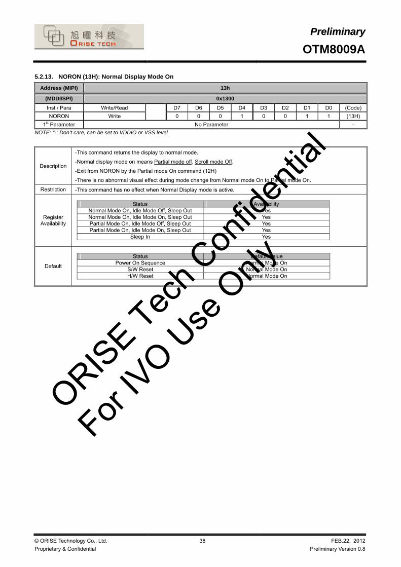
PPrreelliimmiinnaarryy
OTM8009A
© ORISE Technology Co., Ltd.
Proprietary & Confidential
38 FEB.22, 2012
Preliminary Version 0.8
5.2.13. NORON (13H): Normal Display Mode On
Address (MIPI) 13h
(MDDI/SPI) 0x1300
Inst / Para Write/Read D7 D6 D5 D4 D3 D2 D1 D0 (Code)
NORON Write
0 0 0 1 0 0 1 1 (13H)
1st Parameter No Parameter -
NOTE: “-” Don’t care, can be set to VDDIO or VSS level
Description
-This command returns the display to normal mode.
-Normal display mode on means Partial mode off, Scroll mode Off.
-Exit from NORON by the Partial mode On command (12H)
-There is no abnormal visual effect during mode change from Normal mode On to Partial mode On.
Restriction -This command has no effect when Normal Display mode is active.
Register Availability
Status Availability
Normal Mode On, Idle Mode Off, Sleep Out Yes Normal Mode On, Idle Mode On, Sleep Out Yes Partial Mode On, Idle Mode Off, Sleep Out Yes Partial Mode On, Idle Mode On, Sleep Out Yes
Sleep In Yes
Default
Status Default Value
Power On Sequence Normal Mode On S/W Reset Normal Mode On H/W Reset Normal Mode On
ORISE Tec
h Con
fiden
tial
For IV
O Use
Only

PPrreelliimmiinnaarryy
OTM8009A
© ORISE Technology Co., Ltd.
Proprietary & Confidential
39 FEB.22, 2012
Preliminary Version 0.8
5.2.14. INVOFF (20h) : Display Inversion Off
Address (MIPI) 20h
(MDDI/SPI) 0x2000
Write/Read D7 D6 D5 D4 D3 D2 D1 D0 HEX
Command Write 0 0 1 0 0 0 0 0 20
Parameter No parameter
Description
This command is used to recover from display inversion mode.
This command makes no change of contents of frame memory.
This command does not change any other status.
X = Don’t care
Restrictions This command has no effect when module is already in inversion off mode.
Register
Availability
Status Availability
Normal Mode, Idle Mode Off, Sleep Out Yes
Normal Mode, Idle Mode On, Sleep Out Yes
Partial Mode, Idle Mode Off, Sleep Out Yes
Partial Mode, Idle Mode On, Sleep Out Yes
Sleep In Yes
Default
Status Default value
Power On Sequence Display Inversion Off
SW Reset Display Inversion Off
HW Reset Display Inversion Off
ORISE Tec
h Con
fiden
tial
For IV
O Use
Only

PPrreelliimmiinnaarryy
OTM8009A
© ORISE Technology Co., Ltd.
Proprietary & Confidential
40 FEB.22, 2012
Preliminary Version 0.8
5.2.15. INVON (21h) : Display Inversion On
Address (MIPI) 21h
(MDDI/SPI) 0x2100
Write/Read D7 D6 D5 D4 D3 D2 D1 D0 HEX
Command Write 0 0 1 0 0 0 0 1 21
1st parameter
Parameter No parameter
Description
This command is used to enter into display inversion mode.
This command makes no change of contents of frame memory. Every bit is inverted from
the frame memory to the display.
This command does not change any other status.
X = Don’t care
Restrictions This command has no effect when module is already in inversion on mode.
Register
Availability
Status Availability
Normal Mode, Idle Mode Off, Sleep Out Yes
Normal Mode, Idle Mode On, Sleep Out Yes
Partial Mode, Idle Mode Off, Sleep Out Yes
Partial Mode, Idle Mode On, Sleep Out Yes
Sleep In Yes
Default
Status Default value
Power On Sequence Display Inversion Off
SW Reset Display Inversion Off
HW Reset Display Inversion Off
ORISE Tec
h Con
fiden
tial
For IV
O Use
Only

PPrreelliimmiinnaarryy
OTM8009A
© ORISE Technology Co., Ltd.
Proprietary & Confidential
41 FEB.22, 2012
Preliminary Version 0.8
5.2.16. ALLPOFF (22H): All Pixels Off
Address (MIPI) 22h
(MDDI/SPI) 0x2200
Inst / Para Write/Read D7 D6 D5 D4 D3 D2 D1 D0 (Code)
ALLPOOFF Write
0 0 1 0 0 0 1 0 (22H)
1st Parameter No Parameter -
NOTE: “-” Don’t care, can be set to VDDIO or VSS level
Description
- This command turns the display panel black in ‘Sleep Out’ –mode and a status of the ‘Display On/Off’ –register can be ‘on’ or ‘off’.
- This command makes no change of contents of frame memory (or MIP). This command does not change any other status.
- ‘All Pixels On’, ’Normal Display Mode On’ or ’Partial Mode On’ – commands are used to leave this mode.
- The display panel is showing the content of the frame memory after ‘Normal Display Mode On’ and ‘Partial Mode On’ -commands.
Restriction - This command has no effect when module is already in all pixels off mode.
Register Availability
Status Availability
Normal Mode On, Idle Mode Off, Sleep Out Yes Normal Mode On, Idle Mode On, Sleep Out Yes Partial Mode On, Idle Mode Off, Sleep Out Yes Partial Mode On, Idle Mode On, Sleep Out Yes
Sleep In Yes
Default
Status Default Value
Power On Sequence Off S/W Reset Off H/W Reset Off
ORISE Tec
h Con
fiden
tial
For IV
O Use
Only

PPrreelliimmiinnaarryy
OTM8009A
© ORISE Technology Co., Ltd.
Proprietary & Confidential
42 FEB.22, 2012
Preliminary Version 0.8
5.2.17. ALLPON (23H): All Pixels On
Address (MIPI) 23h
(MDDI/SPI) 0x2300
Inst / Para Write/Read D7 D6 D5 D4 D3 D2 D1 D0 (Code)
ALLPOON Write
0 0 1 0 0 0 1 1 (23H)
1st Parameter No Parameter -
NOTE: “-” Don’t care, can be set to VDDIO or VSS level
Description
- This command turns the display panel white in ‘Sleep out ‘ –mode and a status of the ‘Display On/Off’ –register can be ‘on’ or ‘off’.
- This command makes no change of contents of frame memory (or MIP).
- This command does not change any other status.
- ‘All Pixels Off’, ’Normal Display Mode On’ or ’Partial Mode On’ – commands are used to leave this mode.
- The display is showing the content of the frame memory after ‘Normal Display Mode On’ and ‘Partial Mode On’ –commands.
Restriction - This command has no effect when module is already in all pixels on mode.
Register Availability
Status Availability
Normal Mode On, Idle Mode Off, Sleep Out Yes Normal Mode On, Idle Mode On, Sleep Out Yes Partial Mode On, Idle Mode Off, Sleep Out Yes Partial Mode On, Idle Mode On, Sleep Out Yes
Sleep In Yes
Default
Status Default Value
Power On Sequence Off S/W Reset Off H/W Reset Off
ORISE Tec
h Con
fiden
tial
For IV
O Use
Only

PPrreelliimmiinnaarryy
OTM8009A
© ORISE Technology Co., Ltd.
Proprietary & Confidential
43 FEB.22, 2012
Preliminary Version 0.8
5.2.18. GAMSET (26H): Gamma Set
Address (MIPI) 26h
(MDDI/SPI) 0x2600
Inst / Para Write/Read D7 D6 D5 D4 D3 D2 D1 D0 (Code)
GAMSET Write 0 0 1 0 0 1 1 0 (26H)
1st Parameter Write
GC7 GC6 GC5 GC4 GC3 GC2 GC1 GC0 01h
NOTE: “-” Don’t care, can be set to VDDIO or VSS level
Description
-This command is used to select the desired Gamma curve for the current display. A maximum of 4 curves can be selected. The curve is selected by setting the appropriate bit in the parameter as described in the Table.
GC [7:0] Parameter Curve Selected
01h GC0 Gamma Curve 1 (G2.2)
02h GC1 Gamma Curve 2 (G1.8)
04h GC2 Gamma Curve 3 (G2.5)
08h GC3 Gamma Curve 4 (G1.0)
Note: 1. All other values are undefined. 2. In the Gamma separate mode ignore this command.
Restriction -Values of GC [7:0] not shown in table above are invalid and will not change the current selected Gamma curve until valid is received.
Register Availability
Status Availability
Normal Mode On, Idle Mode Off, Sleep Out Yes Normal Mode On, Idle Mode On, Sleep Out Yes Partial Mode On, Idle Mode Off, Sleep Out Yes Partial Mode On, Idle Mode On, Sleep Out Yes
Sleep In Yes
Default
Status Default Value
Power On Sequence 01h S/W Reset 01h H/W Reset 01h
ORISE Tec
h Con
fiden
tial
For IV
O Use
Only

PPrreelliimmiinnaarryy
OTM8009A
© ORISE Technology Co., Ltd.
Proprietary & Confidential
44 FEB.22, 2012
Preliminary Version 0.8
5.2.19. DISPOFF (28H): Display Off
Address (MIPI) 28h
(MDDI/SPI) 0x2800
Inst / Para Write/Read D7 D6 D5 D4 D3 D2 D1 D0 (Code)
DISPOFF Write
0 0 1 0 1 0 0 0 (28H)
1st Parameter No Parameter -
NOTE: “-” Don’t care, can be set to VDDIO or VSS level
Description
-This command is used to enter into DISPLAY OFF mode. In this mode, the output from Frame Memory is disables and blank page inserted.
-This command makes no change of contents of frame memory.
-This command does not change any other status.
-There will be no abnormal visible effect on the display.
-Exit from this command by Display On (29H)
Restriction -This command has no effect when module is already in Display Off mode.
Register Availability
Status Availability
Normal Mode On, Idle Mode Off, Sleep Out Yes Normal Mode On, Idle Mode On, Sleep Out Yes Partial Mode On, Idle Mode Off, Sleep Out Yes Partial Mode On, Idle Mode On, Sleep Out Yes
Sleep In Yes
Default
Status Default Value
Power On Sequence Display off S/W Reset Display off H/W Reset Display off
ORISE Tec
h Con
fiden
tial
For IV
O Use
Only
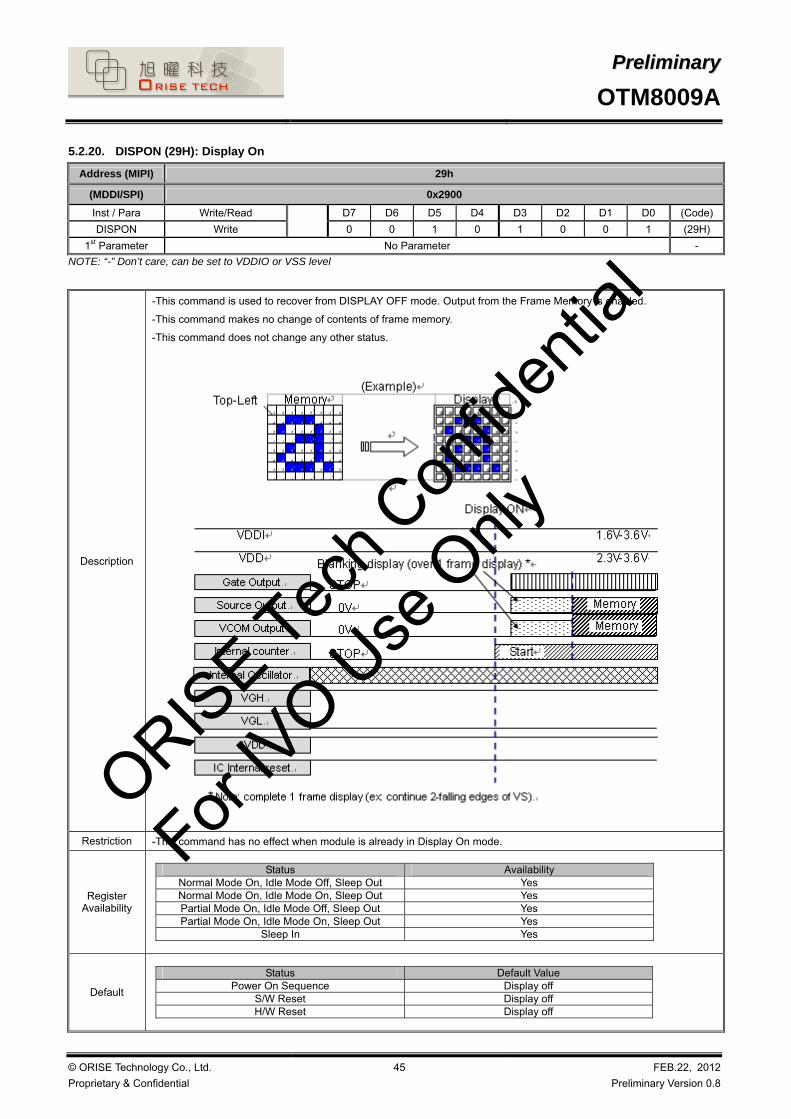
PPrreelliimmiinnaarryy
OTM8009A
© ORISE Technology Co., Ltd.
Proprietary & Confidential
45 FEB.22, 2012
Preliminary Version 0.8
5.2.20. DISPON (29H): Display On
Address (MIPI) 29h
(MDDI/SPI) 0x2900
Inst / Para Write/Read D7 D6 D5 D4 D3 D2 D1 D0 (Code)
DISPON Write
0 0 1 0 1 0 0 1 (29H)
1st Parameter No Parameter -
NOTE: “-” Don’t care, can be set to VDDIO or VSS level
Description
-This command is used to recover from DISPLAY OFF mode. Output from the Frame Memory is enabled.
-This command makes no change of contents of frame memory.
-This command does not change any other status.
Restriction -This command has no effect when module is already in Display On mode.
Register Availability
Status Availability
Normal Mode On, Idle Mode Off, Sleep Out Yes Normal Mode On, Idle Mode On, Sleep Out Yes Partial Mode On, Idle Mode Off, Sleep Out Yes Partial Mode On, Idle Mode On, Sleep Out Yes
Sleep In Yes
Default
Status Default Value
Power On Sequence Display off S/W Reset Display off H/W Reset Display off
ORISE Tec
h Con
fiden
tial
For IV
O Use
Only

PPrreelliimmiinnaarryy
OTM8009A
© ORISE Technology Co., Ltd.
Proprietary & Confidential
46 FEB.22, 2012
Preliminary Version 0.8
5.2.21. CASET (2AH): Column Address Set
Address (MIPI) 2Ah
(MDDI/SPI) 0x2A00 ~ 0x2A03
Inst / Para Write/Read D7 D6 D5 D4 D3 D2 D1 D0 (Code)
CASET Write 0 0 1 0 1 0 1 0 (2AH)
1st Parameter Write XS15 XS14 XS13 XS12 XS11 XS10 XS9 XS8 00h
2nd Parameter Write XS7 XS6 XS5 XS4 XS3 XS2 XS1 XS0 00h
3rd Parameter Write XE15 XE14 XE13 XE12 XE11 XE10 XE9 XE8 01h
4th Parameter Write
XE7 XE6 XE5 XE4 XE3 XE2 XE1 XE0 DFh
NOTE: “-” Don’t care, can be set to VDDIO or VSS level
Description
-This command is used to define area of frame memory where MCU can access.
-This command makes no change on the other driver status.
-The value of XS [15:0] and XE [15:0] are referred when RAMWR command comes.
-Each value represents one column line in the Frame Memory.
Restriction
XS [15:0] always must be equal to or less than XE [15:0]
When XS [15:0] or XE [15:0] is greater than maximum address like below, data of out of range will be ignored.
Register Availability
Status Availability
Normal Mode On, Idle Mode Off, Sleep Out Yes Normal Mode On, Idle Mode On, Sleep Out Yes Partial Mode On, Idle Mode Off, Sleep Out Yes Partial Mode On, Idle Mode On, Sleep Out Yes
Sleep In Yes ORIS
E Tech C
onfid
entia
l
For IV
O Use
Only

PPrreelliimmiinnaarryy
OTM8009A
© ORISE Technology Co., Ltd.
Proprietary & Confidential
47 FEB.22, 2012
Preliminary Version 0.8
Default
480x864 Resolution
Default Value Status
XS [15:0] XE [15:0] (MV=’0’) XE [15:0] (MV=’1’)
Power On Sequence 01DFh (479d)
S/W Reset 01DFh (479d) 035Fh (863d)
H/W Reset
0000h
01DFh (479d)
480x854 Resolution
Default Value Status
XS [15:0] XE [15:0] (MV=’0’) XE [15:0] (MV=’1’)
Power On Sequence 01DFh (479d)
S/W Reset 01DFh (479d) 0355h (853d)
H/W Reset
0000h
01DFh (479d)
480x800 Resolution (IC Default Setting)
Default Value Status
XS [15:0] XE [15:0] (MV=’0’) XE [15:0] (MV=’1’)
Power On Sequence 01DFh (479d)
S/W Reset 01DFh (479d) 031Fh (799d)
H/W Reset
0000h
01DFh (479d)
480x720 Resolution
Default Value Status
XS [15:0] XE [15:0] (MV=’0’) XE [15:0] (MV=’1’)
Power On Sequence 01DFh (479d)
S/W Reset 01DFh (479d) 02CFh (719d)
H/W Reset
0000h
01DFh (479d)
480x640 Resolution
Default Value Status
XS [15:0] XE [15:0] (MV=’0’) XE [15:0] (MV=’1’)
Power On Sequence 01DFh (479d)
S/W Reset 01DFh (479d) 027Fh (639d)
H/W Reset
0000h
01DFh (479d)
480x480 Resolution
Default Value Status
XS [15:0] XE [15:0] (MV=’0’) XE [15:0] (MV=’1’)
Power On Sequence 01DFh (479d)
S/W Reset 01DFh (479d) 01DFh (479d)
H/W Reset
0000h
01DFh (479d)
480x360 Resolution
Default Value Status
XS [15:0] XE [15:0] (MV=’0’) XE [15:0] (MV=’1’)
Power On Sequence 01DFh (479d)
S/W Reset 01DFh (479d) 0167h (359d)
H/W Reset
0000h
01DFh (479d)
ORISE Tec
h Con
fiden
tial
For IV
O Use
Only

PPrreelliimmiinnaarryy
OTM8009A
© ORISE Technology Co., Ltd.
Proprietary & Confidential
48 FEB.22, 2012
Preliminary Version 0.8
5.2.22. PASET (2BH): Page Address Set
Address (MIPI) 2Bh
(MDDI/SPI) 0x2B00 ~ 0x2B03
Inst / Para Write/Read D7 D6 D5 D4 D3 D2 D1 D0 (Code)
RASET Write 0 0 1 0 1 0 1 1 (2BH)
1st Parameter Write YS15 YS14 YS13 YS12 YS11 YS10 YS9 YS8 00h
2nd Parameter Write YS7 YS6 YS5 YS4 YS3 YS2 YS1 YS0 00h
3rd Parameter Write YE15 YE14 YE13 YE12 YE11 YE10 YE9 YE8 03h
4th Parameter Write
YE7 YE6 YE5 YE4 YE3 YE2 YE1 YE0 60h
NOTE: “-” Don’t care, can be set to VDDIO or VSS level
Description
-This command is used to define area of frame memory where MCU can access.
-This command makes no change on the other driver status.
-The value of YS [15:0] and YE [15:0] are referred when RAMWR command comes.
-Each value represents one column line in the Frame Memory.
Restriction
YS [15:0] always must be equal to or less than YE [15:0]
When YS [15:0] or YE [15:0] are greater than maximum row address like below, data of out of range will be ignored.
Register Availability
Status Availability
Normal Mode On, Idle Mode Off, Sleep Out Yes Normal Mode On, Idle Mode On, Sleep Out Yes Partial Mode On, Idle Mode Off, Sleep Out Yes Partial Mode On, Idle Mode On, Sleep Out Yes
Sleep In Yes ORIS
E Tech C
onfid
entia
l
For IV
O Use
Only

PPrreelliimmiinnaarryy
OTM8009A
© ORISE Technology Co., Ltd.
Proprietary & Confidential
49 FEB.22, 2012
Preliminary Version 0.8
Default
480x864 Resolution
Default Value Status
YS [15:0] YE [15:0] (MV=’0’) YE [15:0] (MV=’1’)
Power On Sequence 035Fh (863d)
S/W Reset 035Fh (863d) 01DFh (479d)
H/W Reset
0000h
035Fh (863d)
480x854 Resolution
Default Value Status
YS [15:0] YE [15:0] (MV=’0’) YE [15:0] (MV=’1’)
Power On Sequence 0355h (853d)
S/W Reset 0355h (853d) 01DFh (479d)
H/W Reset
0000h
0355h (853d)
480x800 Resolution (IC Default Setting)
Default Value Status
YS [15:0] YE [15:0] (MV=’0’) YE [15:0] (MV=’1’)
Power On Sequence 031Fh (799d)
S/W Reset 031Fh (799d) 01DFh (479d)
H/W Reset
0000h
031Fh (799d)
480x720 Resolution
Default Value Status
YS [15:0] YE [15:0] (MV=’0’) YE [15:0] (MV=’1’)
Power On Sequence 02CFh (719d)
S/W Reset 02CFh (719d) 01DFh (479d)
H/W Reset
0000h
02CFh (719d)
480x640 Resolution
Default Value Status
YS [15:0] YE [15:0] (MV=’0’) YE [15:0] (MV=’1’)
Power On Sequence 027Fh (639d)
S/W Reset 027Fh (639d) 01DFh (479d)
H/W Reset
0000h
027Fh (639d)
480x480 Resolution
Default Value Status
YS [15:0] YE [15:0] (MV=’0’) YE [15:0] (MV=’1’)
Power On Sequence 01DFh (479d)
S/W Reset 01DFh (479d) 01DFh (479d)
H/W Reset
0000h
01DFh (479d)
480x360 Resolution
Default Value Status
YS [15:0] YE [15:0] (MV=’0’) YE [15:0] (MV=’1’)
Power On Sequence 0167h (359d)
S/W Reset 0167h (359d) 01DFh (479d)
H/W Reset
0000h
0167h (359d)
ORISE Tec
h Con
fiden
tial
For IV
O Use
Only

PPrreelliimmiinnaarryy
OTM8009A
© ORISE Technology Co., Ltd.
Proprietary & Confidential
50 FEB.22, 2012
Preliminary Version 0.8
5.2.23. RAMWR (2CH): Memory Write
Address (MIPI) 2Ch
(MDDI/SPI) 0x2C00
Inst / Para Write/Read D7 D6 D5 D4 D3 D2 D1 D0 (Code)
RAMWR Write 0 0 1 0 1 1 0 0 (2CH)
1st Parameter Write D7 D6 D5 D4 D3 D2 D1 D0 -
∣ Write ∣ ∣ ∣ ∣ ∣ ∣ ∣ ∣ ∣
Nth Parameter Write
D7 D6 D5 D4 D3 D2 D1 D0 -
NOTE: “-” Don’t care, can be set to VDDIO or VSS level
Description
-This command is used to transfer data from MCU to frame memory.
-This command makes no change to the other driver status.
-When this command is accepted, the column register and the row register are reset to the Start Column/Start Row positions.
-The Start Column/Start Row positions are different in accordance with MADCTR setting.
-Sending any other command can stop Frame Write.
Restriction
In all color modes, there is no restriction on length of parameters.
480x864 Resolution
480x864x24-bits memory can be written by this command Memory range: (0000h,0000h) -> (01DFh, 035Fh)
Register Availability
Status Availability
Normal Mode On, Idle Mode Off, Sleep Out Yes Normal Mode On, Idle Mode On, Sleep Out Yes Partial Mode On, Idle Mode Off, Sleep Out Yes Partial Mode On, Idle Mode On, Sleep Out Yes
Sleep In Yes
Default
Status Default Value
Power On Sequence Contents of memory is set randomly S/W Reset Contents of memory is not cleared H/W Reset Contents of memory is not cleared
ORISE Tec
h Con
fiden
tial
For IV
O Use
Only

PPrreelliimmiinnaarryy
OTM8009A
© ORISE Technology Co., Ltd.
Proprietary & Confidential
51 FEB.22, 2012
Preliminary Version 0.8
5.2.24. RAMRD (2EH): Memory Read
Address (MIPI) 2Eh
(MDDI/SPI) 0x2E00
Inst / Para Write/Read D7 D6 D5 D4 D3 D2 D1 D0 (Code)
RAMRD Write 0 0 1 0 1 1 1 0 (2EH)
1st Parameter Read D7 D6 D5 D4 D3 D2 D1 D0 -
∣ Read ∣ ∣ ∣ ∣ ∣ ∣ ∣ ∣ ∣
(N+1)th Parameter Read
D7 D6 D5 D4 D3 D2 D1 D0 -
NOTE: “-” Don’t care, can be set to VDDIO or VSS level
Description
-This command is used to transfer data from frame memory to MCU.
-This command makes no change to the other driver status.
-When this command is accepted, the column register and the row register are reset to the Start Column/Start Row positions.
-The Start Column/Start Row positions are different in accordance with MADCTR setting.
-Then D[23:0] is read back from the frame memory and the column register and the row register incremented.
-Frame Read can be canceled by sending any other command.
.
Restriction -In all color modes, the Frame Read is always 24-bits and there is no restriction on length of parameters.
Register Availability
Status Availability
Normal Mode On, Idle Mode Off, Sleep Out Yes Normal Mode On, Idle Mode On, Sleep Out Yes Partial Mode On, Idle Mode Off, Sleep Out Yes Partial Mode On, Idle Mode On, Sleep Out Yes
Sleep In Yes
Default
Status Default Value
Power On Sequence Contents of memory is set randomly S/W Reset Contents of memory is not cleared H/W Reset Contents of memory is not cleared
ORISE Tec
h Con
fiden
tial
For IV
O Use
Only

PPrreelliimmiinnaarryy
OTM8009A
© ORISE Technology Co., Ltd.
Proprietary & Confidential
52 FEB.22, 2012
Preliminary Version 0.8
5.2.25. PTLAR (30H): Partial Area
Address (MIPI) 30h
(MDDI/SPI) 0x3000 ~ 0x3003
Inst / Para Write/Read D7 D6 D5 D4 D3 D2 D1 D0 (Code)
PTLAR Write 0 0 1 1 0 0 0 0 (30H)
1st Parameter Write PSL15 PSL14 PSL13 PSL12 PSL11 PSL10 PSL9 PSL8 00h
2nd Parameter Write PSL7 PSL6 PSL5 PSL4 PSL3 PSL2 PSL1 PSL0 00h
3rd Parameter Write PEL15 PEL14 PEL13 PEL12 PEL11 PEL10 PEL9 PEL8
4th Parameter Write
PEL7 PEL6 PEL5 PEL4 PEL3 PEL2 PEL1 PEL0
NOTE: “-” Don’t care, can be set to VDDIO or VSS level
Description
-This command defines the partial mode’s display area.
-There are 4 parameters associated with this command, the first defines the Start Row (PSL) and the second the End Row (PEL), as illustrated in the figures below. PSL and PEL refer to the Frame Memory row address counter.
-If End Row = Start Row then the Partial Area will be one row deep.
ORISE Tec
h Con
fiden
tial
For IV
O Use
Only

PPrreelliimmiinnaarryy
OTM8009A
© ORISE Technology Co., Ltd.
Proprietary & Confidential
53 FEB.22, 2012
Preliminary Version 0.8
Restriction
-PEL [15:0] always must be equal to or less than PSL [15:0]
-When PEL [15:0] or PSL [15:0] are greater than maximum row address like below, data of out of range will be ignored.
480x864 memory base
(Parameter range: 0d PSL [15:0] PEL [15:0] 863d (35Fh)) If the “PSL” or “PEL” are large then 863d, it become 863d
Register Availability
Status Availability
Normal Mode On, Idle Mode Off, Sleep Out Yes Normal Mode On, Idle Mode On, Sleep Out Yes Partial Mode On, Idle Mode Off, Sleep Out Yes Partial Mode On, Idle Mode On, Sleep Out Yes
Sleep In Yes
Default
480x864 memory base
Default Value Status
PSL [15:0] PEL [15:0] Power On Sequence
S/W Reset H/W Reset
0000h 035Fh
ORISE Tec
h Con
fiden
tial
For IV
O Use
Only

PPrreelliimmiinnaarryy
OTM8009A
© ORISE Technology Co., Ltd.
Proprietary & Confidential
54 FEB.22, 2012
Preliminary Version 0.8
5.2.26. TEOFF (34H): Tearing Effect Line OFF
Address (MIPI) 34h
(MDDI/SPI) 0x3400
Inst / Para Write/Read D7 D6 D5 D4 D3 D2 D1 D0 (Code)
TEOFF Write
0 0 1 1 0 1 0 0 (34H)
1st Parameter No Parameter -
NOTE: “-” Don’t care, can be set to VDDIO or VSS level
Description -This command is used to turn OFF (Active Low) the Tearing Effect output signal from the TE signal line.
Restriction -This command has no effect when Tearing Effect output is already OFF.
Register Availability
Status Availability
Normal Mode On, Idle Mode Off, Sleep Out Yes Normal Mode On, Idle Mode On, Sleep Out Yes Partial Mode On, Idle Mode Off, Sleep Out Yes Partial Mode On, Idle Mode On, Sleep Out Yes
Sleep In Yes
Default
Status Default Value
Power On Sequence S/W Reset H/W Reset
OFF
ORISE Tec
h Con
fiden
tial
For IV
O Use
Only

PPrreelliimmiinnaarryy
OTM8009A
© ORISE Technology Co., Ltd.
Proprietary & Confidential
55 FEB.22, 2012
Preliminary Version 0.8
5.2.27. TEON (35H): Tearing Effect Line ON
Address (MIPI) 35h
(MDDI/SPI) 0x3500
Inst / Para Write/Read D7 D6 D5 D4 D3 D2 D1 D0 (Code)
TEON Write 0 0 1 1 0 1 0 1 (35H)
1st Parameter Write
0 0 0 0 0 0 0 TELOM 00h
NOTE: “-” Don’t care, can be set to VDDIO or VSS level
Description
-This command is used to turn ON the Tearing Effect output signal from the TE signal line.
-This output is not affected by changing MADCTR bit ML.
-The Tearing Effect Line On has one parameter, which describes the mode of the Tearing Effect Output Line. (“-“=Don’t Care).
-When M=’0’:
The Tearing Effect Output line consists of V-Blanking information only.
-When M=’1’:
The Tearing Effect Output line consists of both V-Blanking and H-Blinking information.
Note: During Sleep In Mode with Tearing Effect Line On, Tearing Effect Output pin will be active Low.
Restriction -This command has no effect when Tearing Effect output is already OFF.
-In MIPI mode, only the Tearing Effect Output line consists of V-Blanking information is available (M=’0’).
Register Availability
Status Availability
Normal Mode On, Idle Mode Off, Sleep Out Yes Normal Mode On, Idle Mode On, Sleep Out Yes Partial Mode On, Idle Mode Off, Sleep Out Yes Partial Mode On, Idle Mode On, Sleep Out Yes
Sleep In Yes
Default
Status Default Value
Power On Sequence S/W Reset H/W Reset
OFF & TELOM=0
ORISE Tec
h Con
fiden
tial
For IV
O Use
Only

PPrreelliimmiinnaarryy
OTM8009A
© ORISE Technology Co., Ltd.
Proprietary & Confidential
56 FEB.22, 2012
Preliminary Version 0.8
5.2.28. MADCTR (36H): Memory Data Access Control
Address (MIPI) 36h
(MDDI/SPI) 0x3600
Inst / Para Write/Read D7 D6 D5 D4 D3 D2 D1 D0 (Code)
MADCTR Write 0 0 1 1 0 1 1 0 (36H)
1st Parameter Write
MY MX MV ML RGB 0 0 0 00h
NOTE: “-” Don’t care, can be set to VDDIO or VSS level
Description
- This command has no effect for driver output, only register value is updated.
-This command defines read/ write scanning direction of frame memory.
-This command makes no change on the other driver status.
-Bit Assignment
Bit NAME DESCRIPTION
MY Row Address Order
MX Column Address Order
MV Row/Column Exchange
These 3bits controls MCU to memory write/read direction.
ML Vertical Refresh Order LCD vertical refresh direction control ‘0’ = LCD vertical refresh Top to Bottom ‘1’ = LCD vertical refresh Bottom to Top
RGB RGB-BGR ORDER Color selector switch control ‘0’ =RGB color filter panel, ‘1’ =BGR color filter panel
ORISE Tec
h Con
fiden
tial
For IV
O Use
Only
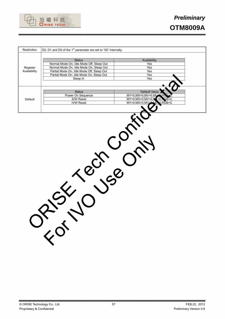
PPrreelliimmiinnaarryy
OTM8009A
© ORISE Technology Co., Ltd.
Proprietary & Confidential
57 FEB.22, 2012
Preliminary Version 0.8
Restriction D2, D1 and D0 of the 1st parameter are set to “00” internally.
Register Availability
Status Availability
Normal Mode On, Idle Mode Off, Sleep Out Yes Normal Mode On, Idle Mode On, Sleep Out Yes Partial Mode On, Idle Mode Off, Sleep Out Yes Partial Mode On, Idle Mode On, Sleep Out Yes
Sleep In Yes
Default
Status Default Value
Power On Sequence MY=0,MX=0,MV=0,ML=0,RGB=0, S/W Reset MY=0,MX=0,MV=0,ML=0,RGB=0, H/W Reset MY=0,MX=0,MV=0,ML=0,RGB=0,
ORISE Tec
h Con
fiden
tial
For IV
O Use
Only

PPrreelliimmiinnaarryy
OTM8009A
© ORISE Technology Co., Ltd.
Proprietary & Confidential
58 FEB.22, 2012
Preliminary Version 0.8
5.2.29. IDMOFF (38H): Idle Mode Off
Address (MIPI) 38h
(MDDI/SPI) 0x3800
Inst / Para Write/Read D7 D6 D5 D4 D3 D2 D1 D0 (Code)
IDMOFF Write
0 0 1 1 1 0 0 0 (38H)
1st Parameter No Parameter -
NOTE: “-” Don’t care, can be set to VDDIO or VSS level
Description
-This command is used to recover from Idle mode on.
-There will be no abnormal visible effect on the display mode change transition.
-In the idle off mode,
1. LCD can display 4k, 65k, 262k and 16.7M –colors. 2. Normal frame frequency is applied.
Restriction -This command has no effect when module is already in idle off mode.
Register Availability
Status Availability
Normal Mode On, Idle Mode Off, Sleep Out Yes Normal Mode On, Idle Mode On, Sleep Out Yes Partial Mode On, Idle Mode Off, Sleep Out Yes Partial Mode On, Idle Mode On, Sleep Out Yes
Sleep In Yes
Default
Status Default Value
Power On Sequence Idle Mode Off S/W Reset Idle Mode Off H/W Reset Idle Mode Off
ORISE Tec
h Con
fiden
tial
For IV
O Use
Only
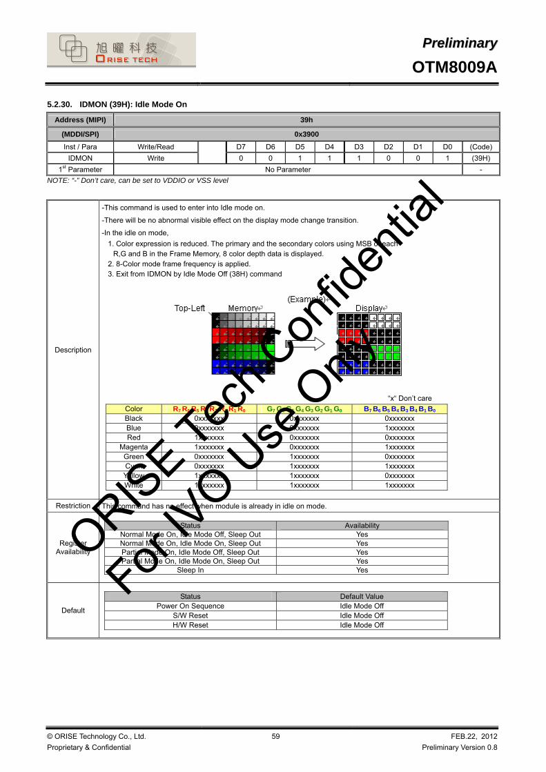
PPrreelliimmiinnaarryy
OTM8009A
© ORISE Technology Co., Ltd.
Proprietary & Confidential
59 FEB.22, 2012
Preliminary Version 0.8
5.2.30. IDMON (39H): Idle Mode On
Address (MIPI) 39h
(MDDI/SPI) 0x3900
Inst / Para Write/Read D7 D6 D5 D4 D3 D2 D1 D0 (Code)
IDMON Write
0 0 1 1 1 0 0 1 (39H)
1st Parameter No Parameter -
NOTE: “-” Don’t care, can be set to VDDIO or VSS level
Description
-This command is used to enter into Idle mode on.
-There will be no abnormal visible effect on the display mode change transition.
-In the idle on mode,
1. Color expression is reduced. The primary and the secondary colors using MSB of each R,G and B in the Frame Memory, 8 color depth data is displayed.
2. 8-Color mode frame frequency is applied. 3. Exit from IDMON by Idle Mode Off (38H) command
“x“ Don’t care
Color R7 R6 R5 R4 R3 R2 R1 R0 G7 G6 G5 G4 G3 G2 G1 G0 B7 B6 B5 B4 B3 B4 B1 B0 Black 0xxxxxxx 0xxxxxxx 0xxxxxxx Blue 0xxxxxxx 0xxxxxxx 1xxxxxxx Red 1xxxxxxx 0xxxxxxx 0xxxxxxx
Magenta 1xxxxxxx 0xxxxxxx 1xxxxxxx Green 0xxxxxxx 1xxxxxxx 0xxxxxxx Cyan 0xxxxxxx 1xxxxxxx 1xxxxxxx Yellow 1xxxxxxx 1xxxxxxx 0xxxxxxx White 1xxxxxxx 1xxxxxxx 1xxxxxxx
Restriction This command has no effect when module is already in idle on mode.
Register Availability
Status Availability
Normal Mode On, Idle Mode Off, Sleep Out Yes Normal Mode On, Idle Mode On, Sleep Out Yes Partial Mode On, Idle Mode Off, Sleep Out Yes Partial Mode On, Idle Mode On, Sleep Out Yes
Sleep In Yes
Default
Status Default Value
Power On Sequence Idle Mode Off S/W Reset Idle Mode Off H/W Reset Idle Mode Off
ORISE Tec
h Con
fiden
tial
For IV
O Use
Only

PPrreelliimmiinnaarryy
OTM8009A
© ORISE Technology Co., Ltd.
Proprietary & Confidential
60 FEB.22, 2012
Preliminary Version 0.8
5.2.31. COLMOD (3AH): Interface Pixel Format
Address (MIPI) 3Ah
(MDDI/SPI) 0x3A00
Inst / Para Write/Read D7 D6 D5 D4 D3 D2 D1 D0 (Code)
COLMOD Write 0 0 1 1 1 0 1 0 (3AH)
1st Parameter Write
VIPF3 VIPF2 VIPF1 VIPF0 D3 IFPF2 IFPF1 IFPF0 77h
NOTE: “-” Don’t care, can be set to VDDIO or VSS level
Description This command is used to define the format of RGB picture data, which is to be transferred via the MCU interface and RGB interface. The formats are shown in the table:
IFPF[2:0] MCU Interface Color Format 011 3 12-bits/pixel 101 5 16-bits/pixel 110 6 18-bits/pixel 111 7 24-bits/pixel
Others are no define and invalid
VIPF[3:0] RGB Interface Color Format 0101 5 16-bits/pixel (1-times data transfer) 0110 6 18-bits/pixel (1-times data transfer) 0111 7 24-bits/pixel (1-times data transfer) 1110 14 24-bits/pixel (3-times data transfer)
Others are no define and invalid Note1: In 12-bits/Pixel, 16-bits/Pixel or 18-bits/Pixel mode, the LUT is applied to transfer data into the Frame Memory. Note2: When RGB I/F the 12-bit/pixel don’t care Note 3: When VIPF[3:0]=”1110”,8-bits data width of 3-times transfer is used to transmit 1 pixel data with the 24-bits color
depth information. Restriction There is no visible effect until the Frame Memory is written to.
Register Availability
Status Availability
Normal Mode On, Idle Mode Off, Sleep Out Yes Normal Mode On, Idle Mode On, Sleep Out Yes Partial Mode On, Idle Mode Off, Sleep Out Yes Partial Mode On, Idle Mode On, Sleep Out Yes
Sleep In Yes
Default
Status Default Value
IFPF[2:0] VIPF[3:0] Power On Sequence 111 (24-bits/pixel) 0111 (24-bits/pixel)
S/W Reset 111 (24-bits/pixel) 0111 (24-bits/pixel) H/W Reset 111 (24-bits/pixel) 0111 (24-bits/pixel)
ORISE Tec
h Con
fiden
tial
For IV
O Use
Only

PPrreelliimmiinnaarryy
OTM8009A
© ORISE Technology Co., Ltd.
Proprietary & Confidential
61 FEB.22, 2012
Preliminary Version 0.8
5.2.32. RAMWRCNT (3CH): Memory Write Continue
Address (MIPI) 3Ch
(MDDI/SPI) 0x3C00
Inst / Para Write/Read D7 D6 D5 D4 D3 D2 D1 D0 (Code)
RAMWRCNT Write 0 0 1 1 1 1 0 0 (3CH)
1st Parameter Write D7 D6 D5 D4 D3 D2 D1 D0 -
∣ Write ∣ ∣ ∣ ∣ ∣ ∣ ∣ ∣ ∣
Nth Parameter Write
D7 D6 D5 D4 D3 D2 D1 D0 -
NOTE: “-” Don’t care, can be set to VDDIO or VSS level
Description
-This command is used to transfer data from MCU to frame memory continuing from the pixel location following the previous 2CH or 3CH command
-This command makes no change to the other driver status.
-When this command is accepted, the column register and the row register are not reset to the Start Column/Start Row positions.
-The Start Column/Start Row positions are different in accordance with MADCTR setting.
-Sending any other command can stop Frame Write.
Restriction
In all color modes, there is no restriction on length of parameters.
480x864 memory base
480x864x24-bits memory can be written by this command Memory range: (0000h,0000h) -> (01DFh, 035Fh)
Register Availability
Status Availability
Normal Mode On, Idle Mode Off, Sleep Out Yes Normal Mode On, Idle Mode On, Sleep Out Yes Partial Mode On, Idle Mode Off, Sleep Out Yes Partial Mode On, Idle Mode On, Sleep Out Yes
Sleep In Yes
Default
Status Default Value
Power On Sequence Contents of memory is set randomly S/W Reset Contents of memory is not cleared H/W Reset Contents of memory is not cleared
ORISE Tec
h Con
fiden
tial
For IV
O Use
Only

PPrreelliimmiinnaarryy
OTM8009A
© ORISE Technology Co., Ltd.
Proprietary & Confidential
62 FEB.22, 2012
Preliminary Version 0.8
5.2.33. RAMRDCNT (3EH): Memory Read Continue
Address (MIPI) 3Eh
(MDDI/SPI) 0x3E00
Inst / Para Write/Read D7 D6 D5 D4 D3 D2 D1 D0 (Code)
RAMRDCNT Write 0 0 1 1 1 1 1 0 (3EH)
1st Parameter Read D7 D6 D5 D4 D3 D2 D1 D0 -
∣ Read ∣ ∣ ∣ ∣ ∣ ∣ ∣ ∣ ∣
(N+1)th Parameter Read
D7 D6 D5 D4 D3 D2 D1 D0 -
NOTE: “-” Don’t care, can be set to VDDIO or VSS level
Description
-This command is used to transfer data from frame memory to MCU if there is wanted to continue memory write after 2EH command.
-This command makes no change to the other driver status.
-When this command is accepted, the column register and the row register are not reset to the Start Column/Start Row positions.
-The Start Column/Start Row positions are different in accordance with MADCTR setting.
-Then D[23:0] is read back from the frame memory and the column register and the row register incremented.
-Frame Read can be canceled by sending any other command.
.
Restriction -In all color modes, the Frame Read is always 24-bits and there is no restriction on length of parameters.
Register Availability
Status Availability
Normal Mode On, Idle Mode Off, Sleep Out Yes Normal Mode On, Idle Mode On, Sleep Out Yes Partial Mode On, Idle Mode Off, Sleep Out Yes Partial Mode On, Idle Mode On, Sleep Out Yes
Sleep In Yes
Default
Status Default Value
Power On Sequence Contents of memory is set randomly S/W Reset Contents of memory is not cleared H/W Reset Contents of memory is not cleared
ORISE Tec
h Con
fiden
tial
For IV
O Use
Only

PPrreelliimmiinnaarryy
OTM8009A
© ORISE Technology Co., Ltd.
Proprietary & Confidential
63 FEB.22, 2012
Preliminary Version 0.8
5.2.34. WRTESCN (44H): Write TE Scan Line
Address (MIPI) 44h
(MDDI/SPI) 0x4400
Inst / Para Write/Read D7 D6 D5 D4 D3 D2 D1 D0 (Code)
WRTESCN Write 0 1 0 0 0 1 0 0 (44H)
1st Parameter Write N15 N14 N13 N12 N11 N10 N9 N8 -
2nd Parameter Write
N7 N6 N5 N4 N3 N2 N1 N0 -
NOTE: “-” Don’t care, can be set to VDDIO or VSS level
Description
-This command turns on the display module’s TE signal when the display module reaches line N.
- When setting N=0, it is equivalent to 35H, M=0.
Restriction -The command takes affect with the end of one frame.
Register Availability
Status Availability
Normal Mode On, Idle Mode Off, Sleep Out Yes Normal Mode On, Idle Mode On, Sleep Out Yes Partial Mode On, Idle Mode Off, Sleep Out Yes Partial Mode On, Idle Mode On, Sleep Out Yes
Sleep In Yes
Default
Status Default Value
Power On Sequence 0000h S/W Reset 0000h H/W Reset 0000h
ORISE Tec
h Con
fiden
tial
For IV
O Use
Only

PPrreelliimmiinnaarryy
OTM8009A
© ORISE Technology Co., Ltd.
Proprietary & Confidential
64 FEB.22, 2012
Preliminary Version 0.8
5.2.35. RDSCNL (45H): Read Scan Line
Address (MIPI) 45h
(MDDI/SPI) 0x4500 ~ 0x4501
Inst / Para Write/Read D7 D6 D5 D4 D3 D2 D1 D0 (Code)
RDSCNL Write 0 1 0 0 0 1 0 1 (45H)
1st Parameter Read N15 N14 N13 N12 N11 N10 N9 N8 xxh
2nd Parameter Read
N7 N6 N5 N4 N3 N2 N1 N0 xxh
NOTE: “-” Don’t care, can be set to VDDIO or VSS level
Description
-This read byte returns the current scan line.
-The 1st parameter: N line MSB
-The 2nd parameter: N line LSB
Restriction None
Register Availability
Status Availability
Normal Mode On, Idle Mode Off, Sleep Out Yes Normal Mode On, Idle Mode On, Sleep Out Yes Partial Mode On, Idle Mode Off, Sleep Out Yes Partial Mode On, Idle Mode On, Sleep Out Yes
Sleep In Yes
Default
Status Default Value
Power On Sequence xxh S/W Reset xxh H/W Reset xxh
ORISE Tec
h Con
fiden
tial
For IV
O Use
Only

PPrreelliimmiinnaarryy
OTM8009A
© ORISE Technology Co., Ltd.
Proprietary & Confidential
65 FEB.22, 2012
Preliminary Version 0.8
5.2.36. WRDISBV (51H) Write Display Brightness
Address (MIPI) 51h
(MDDI/SPI) 0x5100
Inst / Para Write/Read D7 D6 D5 D4 D3 D2 D1 D0 (Code)
WRDISBV Write 0 1 0 1 0 0 0 1 (51H)
1st Parameter Write
DBV
7 DBV
6 DBV
5 DBV
4 DBV
3 DBV
2 DBV
1 DBV
0
00 |
FF NOTE: “-” Don’t care, can be set to VDDIO or VSS level
Description
- This command is used to adjust the brightness value of the display.
- It should be checked what is the relationship between this written value and output brightness of the display. This relationship is defined on the display module specification.
- In principle relationship is that 00h value means the lowest brightness and FFh value means the highest brightness.
Restriction -
Register Availability
Status Availability
Normal Mode On, Idle Mode Off, Sleep Out Yes Normal Mode On, Idle Mode On, Sleep Out Yes Partial Mode On, Idle Mode Off, Sleep Out Yes Partial Mode On, Idle Mode On, Sleep Out Yes
Sleep In Yes
Default
Status Default Value
Power On Sequence 00h S/W Reset 00h H/W Reset 00h
ORISE Tec
h Con
fiden
tial
For IV
O Use
Only

PPrreelliimmiinnaarryy
OTM8009A
© ORISE Technology Co., Ltd.
Proprietary & Confidential
66 FEB.22, 2012
Preliminary Version 0.8
5.2.37. RDDISBV (52H) Read Display Brightness Value
Address (MIPI) 52h
(MDDI/SPI) 0x5200
Inst / Para Write/Read D7 D6 D5 D4 D3 D2 D1 D0 (Code)
RDDISBV Write 0 1 0 1 0 0 1 0 (52H)
1st Parameter Read
DBV
7 DBV
6 DBV
5 DBV
4 DBV
3 DBV
2 DBV
1 DBV
0 xxh
NOTE: “-” Don’t care, can be set to VDDIO or VSS level
Description
- This command returns the brightness value of the display.
- It should be checked what the relationship between this returned value and output brightness of the display. This relationship is defined on the display module specification.
- In principle the relationship is that 00h value means the lowest brightness and FFh value means the highest brightness.
- See command “Write Display Brightness (51H)”.
-This command can be used to read the brightness value of the display also when Display brightness control is in automatic mode.
- Write CTRL Display (53H)” bit DB = ‘1’.
- DBV[7:0] is reset when display is in sleep-in mode.
- DBV[7:0] is ‘0’ when bit BCTRL of “Write CTRL Display (53H)” command is ‘0’.
- DBV[7:0] is manual set brightness specified with “Write CTRL Display (53H)” command when bit BCTRL is ‘1’ and bit A of “Write CTRL Display (53H)” command is ‘0’.
Restriction
Register Availability
Status Availability
Normal Mode On, Idle Mode Off, Sleep Out Yes Normal Mode On, Idle Mode On, Sleep Out Yes Partial Mode On, Idle Mode Off, Sleep Out Yes Partial Mode On, Idle Mode On, Sleep Out Yes
Sleep In Yes
Default
Status Default Value
Power On Sequence 00h S/W Reset 00h H/W Reset 00h
ORISE Tec
h Con
fiden
tial
For IV
O Use
Only

PPrreelliimmiinnaarryy
OTM8009A
© ORISE Technology Co., Ltd.
Proprietary & Confidential
67 FEB.22, 2012
Preliminary Version 0.8
5.2.38. WRCTRLD (53H) Write CTRL Display
Address (MIPI) 53h
(MDDI/SPI) 0x5300
Inst / Para Write/Read D7 D6 D5 D4 D3 D2 D1 D0 (Code)
WRCTRLD Write 0 1 0 1 0 0 1 1 (53H)
1st Parameter Write
- - BCTRL - DD BL - - 00 |
FF NOTE: “-” Don’t care, can be set to VDDIO or VSS level
Description
- This command is used to control ambient light, brightness and gamma settings.
BCTRL:Brightness Control Block On/Off. This bit is always used to switch brightness for display and keyboard.
‘0’ = Off (Brightness registers are 00h, DBV[7..0] and KBV[7..0])
‘1’ = On (Brightness registers are active, according to the other parameters.)
DD:Display Dimming
‘0’ = Display Dimming is off
‘1’ = Display Dimming is on
BL:Backlight On/Off
‘0’ = Off (Completely turn off backlight circuit. Control lines must be low. )
‘1’ = On
- Dimming function is adapted to the brightness registers for display and keyboard when bit BCTRL is changed at DD=1, e.g. BCTRL: 0 -> 1 or 1-> 0.
- When BL bit change from “On” to “Off”, backlight is turned off
Restriction
Register Availability
Status Availability
Normal Mode On, Idle Mode Off, Sleep Out Yes Normal Mode On, Idle Mode On, Sleep Out Yes Partial Mode On, Idle Mode Off, Sleep Out Yes Partial Mode On, Idle Mode On, Sleep Out Yes
Sleep In Yes
Default
Status Default Value
Power On Sequence 00h S/W Reset 00h H/W Reset 00h
ORISE Tec
h Con
fiden
tial
For IV
O Use
Only

PPrreelliimmiinnaarryy
OTM8009A
© ORISE Technology Co., Ltd.
Proprietary & Confidential
68 FEB.22, 2012
Preliminary Version 0.8
5.2.39. RDCTRLD (54H) Read CTRL Display
Address (MIPI) 54h
(MDDI/SPI) 0x5400
Inst / Para Write/Read D7 D6 D5 D4 D3 D2 D1 D0 (Code)
RDCTRLD Write 0 1 0 1 0 1 0 0 (54H)
1st Parameter Read
- - BCTRL - DD BL - - xxh
NOTE: “-” Don’t care, can be set to VDDIO or VSS level
Description
- This command returns ambient light and brightness control values, see command “9.2.35 Write CTRL Display (53H) ”.
BCTRL: Brightness Control Block On/Off. This bit is always used to switch brightness for display and keyboard.
‘0’ = Off
‘1’ = On
DD: Display Dimming
‘0’ = Display Dimming is off
‘1’ = Display Dimming is on
BL: Backlight On/Off, This bit is always controlled by the user
‘0’ = Off (completely turn off backlight circuit)
‘1’ = On
Restriction
Register Availability
Status Availability
Normal Mode On, Idle Mode Off, Sleep Out Yes Normal Mode On, Idle Mode On, Sleep Out Yes Partial Mode On, Idle Mode Off, Sleep Out Yes Partial Mode On, Idle Mode On, Sleep Out Yes
Sleep In Yes
Default
Status Default Value
Power On Sequence 00h S/W Reset 00h H/W Reset 00h
ORISE Tec
h Con
fiden
tial
For IV
O Use
Only

PPrreelliimmiinnaarryy
OTM8009A
© ORISE Technology Co., Ltd.
Proprietary & Confidential
69 FEB.22, 2012
Preliminary Version 0.8
5.2.40. WRCABC (55H) Write Content Adaptive Brightness Control
Address (MIPI) 55h
(MDDI/SPI) 0x5500
Inst / Para Write/Read D7 D6 D5 D4 D3 D2 D1 D0 (Code)
WRCABD Write 0 1 0 1 0 1 0 1 (55H)
1st Parameter Write
- - - - - - C1 C0 xxh
NOTE: “-” Don’t care, can be set to VDDIO or VSS level
Description
- This command is used to set parameters for image content based adaptive brightness control functionality.
- There is possible to use 4 different modes for content adaptive image functionality, which are defined on a table below.
C1 C0 Function 0 0 Off 0 1 User Interface Image (UI) 1 0 Still Picture (ST) 1 1 Moving Image (MV)
Restriction
Register Availability
Status Availability
Normal Mode On, Idle Mode Off, Sleep Out Yes Normal Mode On, Idle Mode On, Sleep Out Yes Partial Mode On, Idle Mode Off, Sleep Out Yes Partial Mode On, Idle Mode On, Sleep Out Yes
Sleep In Yes
Default
Status Default Value
Power On Sequence 00h S/W Reset 00h H/W Reset 00h
ORISE Tec
h Con
fiden
tial
For IV
O Use
Only

PPrreelliimmiinnaarryy
OTM8009A
© ORISE Technology Co., Ltd.
Proprietary & Confidential
70 FEB.22, 2012
Preliminary Version 0.8
5.2.41. RDCABC (56H) Read Content Adaptive Brightness Control
Address (MIPI) 56h
(MDDI/SPI) 0x5600
Inst / Para Write/Read D7 D6 D5 D4 D3 D2 D1 D0 (Code)
RDCABC Write 0 1 0 1 0 1 1 0 (56H)
1st Parameter Read
- - - - - - C1 C0 xxh
NOTE: “-” Don’t care, can be set to VDDIO or VSS level
Description
- This command is used to read the settings for image content based adaptive brightness control functionality.
- There is possible to use 4 different modes for content adaptive image functionality, which are defined on a table below.
C1 C0 Function 0 0 Off 0 1 User Interface Image (UI) 1 0 Still Picture (ST) 1 1 Moving Image (MV)
Restriction
Register Availability
Status Availability
Normal Mode On, Idle Mode Off, Sleep Out Yes Normal Mode On, Idle Mode On, Sleep Out Yes Partial Mode On, Idle Mode Off, Sleep Out Yes Partial Mode On, Idle Mode On, Sleep Out Yes
Sleep In Yes
Default
Status Default Value
Power On Sequence 00h S/W Reset 00h H/W Reset 00h
ORISE Tec
h Con
fiden
tial
For IV
O Use
Only
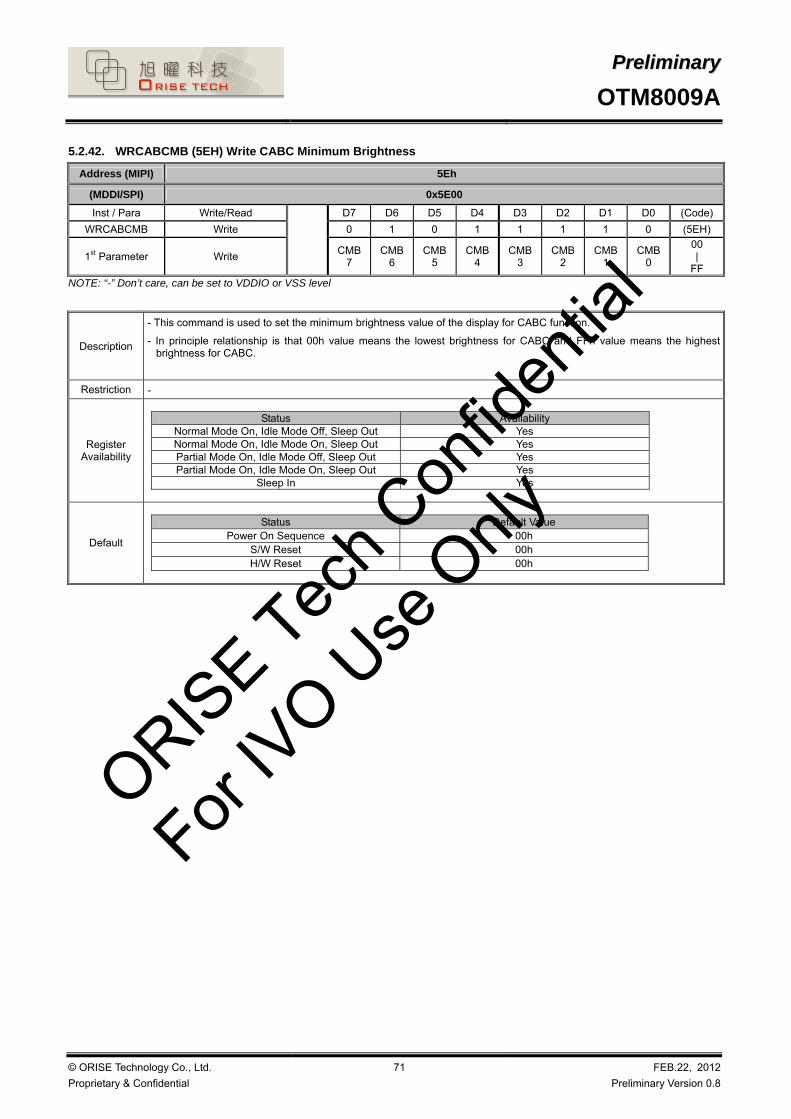
PPrreelliimmiinnaarryy
OTM8009A
© ORISE Technology Co., Ltd.
Proprietary & Confidential
71 FEB.22, 2012
Preliminary Version 0.8
5.2.42. WRCABCMB (5EH) Write CABC Minimum Brightness
Address (MIPI) 5Eh
(MDDI/SPI) 0x5E00
Inst / Para Write/Read D7 D6 D5 D4 D3 D2 D1 D0 (Code)
WRCABCMB Write 0 1 0 1 1 1 1 0 (5EH)
1st Parameter Write
CMB
7 CMB
6 CMB
5 CMB
4 CMB
3 CMB
2 CMB
1 CMB
0
00 |
FF NOTE: “-” Don’t care, can be set to VDDIO or VSS level
Description
- This command is used to set the minimum brightness value of the display for CABC function.
- In principle relationship is that 00h value means the lowest brightness for CABC and FFh value means the highest brightness for CABC.
Restriction -
Register Availability
Status Availability
Normal Mode On, Idle Mode Off, Sleep Out Yes Normal Mode On, Idle Mode On, Sleep Out Yes Partial Mode On, Idle Mode Off, Sleep Out Yes Partial Mode On, Idle Mode On, Sleep Out Yes
Sleep In Yes
Default
Status Default Value
Power On Sequence 00h S/W Reset 00h H/W Reset 00h
ORISE Tec
h Con
fiden
tial
For IV
O Use
Only

PPrreelliimmiinnaarryy
OTM8009A
© ORISE Technology Co., Ltd.
Proprietary & Confidential
72 FEB.22, 2012
Preliminary Version 0.8
5.2.43. RDCABCMB (5FH) Read CABC Minimum Brightness
Address (MIPI) 5Fh
(MDDI/SPI) 0x5F00
Inst / Para Write/Read D7 D6 D5 D4 D3 D2 D1 D0 (Code)
RDCABCMB Write 0 1 0 1 1 1 1 1 (5FH)
1st Parameter Read
CMB
7 CMB
6 CMB
5 CMB
4 CMB
3 CMB
2 CMB
1 CMB
0 xxh
NOTE: “-” Don’t care, can be set to VDDIO or VSS level
Description
- This command returns the minimum brightness value of CABC function.
- In principle the relationship is that 00h value means the lowest brightness and FFh value means the highest brightness.
- See command “Write CABC Minimum Brightness (5EH)”.
Restriction
Register Availability
Status Availability
Normal Mode On, Idle Mode Off, Sleep Out Yes Normal Mode On, Idle Mode On, Sleep Out Yes Partial Mode On, Idle Mode Off, Sleep Out Yes Partial Mode On, Idle Mode On, Sleep Out Yes
Sleep In Yes
Default
Status Default Value
Power On Sequence 00h S/W Reset 00h H/W Reset 00h
ORISE Tec
h Con
fiden
tial
For IV
O Use
Only

PPrreelliimmiinnaarryy
OTM8009A
© ORISE Technology Co., Ltd.
Proprietary & Confidential
73 FEB.22, 2012
Preliminary Version 0.8
5.2.44. RDPWMSDR (68H) Read Automatic Brightness Control Self-diagnostics Result
Address (MIPI) 68h
(MDDI/SPI) 0x6800
Inst / Para Write/Read D7 D6 D5 D4 D3 D2 D1 D0 (Code)
RDPWMSDR Write 0 1 1 0 1 0 0 0 (68H)
1st Parameter Read
D7 D6 0 0 0 0 0 0 x0h
NOTE: “-” Don’t care, can be set to VDDIO or VSS level
Description
- This command indicates the status of the display self-diagnostic results for automatic brightness control after Sleep Out command as described as below:
D7:Register Loading Detection
D6:Functionality Detection
- When “Read Display Self-Diagnostic Result (0FH)” command covers the function for “Read Automatic Brightness Control Self-Diagnostic Result (68H)” command, it is not necessary to implement.
Restriction
Register Availability
Status Availability
Normal Mode On, Idle Mode Off, Sleep Out Yes Normal Mode On, Idle Mode On, Sleep Out Yes Partial Mode On, Idle Mode Off, Sleep Out Yes Partial Mode On, Idle Mode On, Sleep Out Yes
Sleep In Yes
Default
Status Default Value
Power On Sequence 00h S/W Reset 00h H/W Reset 00h
ORISE Tec
h Con
fiden
tial
For IV
O Use
Only

PPrreelliimmiinnaarryy
OTM8009A
© ORISE Technology Co., Ltd.
Proprietary & Confidential
74 FEB.22, 2012
Preliminary Version 0.8
5.2.45. RDBWLB (70H) Read Back/White Low Bits
Address (MIPI) 70h
(MDDI/SPI) 0x7000
Inst / Para Write/Read D7 D6 D5 D4 D3 D2 D1 D0 (Code)
RDBWLB Write 0 1 1 1 0 0 0 0 (70H)
1st Parameter Read
Bkx1
Bkx0
Bky1
Bky0
Wx1
Wx 0
Wy 1
Wy0
xxh
NOTE: “-” Don’t care, can be set to VDDIO or VSS level
Description
- This command returns the lowest bits of black and white color characteristics.
Black: Bkx and Bky
White: Wx and Wy
Restriction
Register Availability
Status Availability
Normal Mode On, Idle Mode Off, Sleep Out Yes Normal Mode On, Idle Mode On, Sleep Out Yes Partial Mode On, Idle Mode Off, Sleep Out Yes Partial Mode On, Idle Mode On, Sleep Out Yes
Sleep In Yes
Default
Status Default Value
Power On Sequence xxh S/W Reset xxh H/W Reset xxh
ORISE Tec
h Con
fiden
tial
For IV
O Use
Only

PPrreelliimmiinnaarryy
OTM8009A
© ORISE Technology Co., Ltd.
Proprietary & Confidential
75 FEB.22, 2012
Preliminary Version 0.8
5.2.46. RDBkx (71H) Read Bkx
Address (MIPI) 71h
(MDDI/SPI) 0x7100
Inst / Para Write/Read D7 D6 D5 D4 D3 D2 D1 D0 (Code)
RDBkx Write 0 1 1 1 0 0 0 1 (71H)
1st Parameter Read
Bkx 9
Bkx 8
Bkx 7
Bkx6
Bkx 5
Bkx 4
Bkx 3
Bkx2
xxh
NOTE: “-” Don’t care, can be set to VDDIO or VSS level
Description - This command returns the Bkx bits (Bkx[9:2]) of black color characteristics.
Restriction
Register Availability
Status Availability
Normal Mode On, Idle Mode Off, Sleep Out Yes Normal Mode On, Idle Mode On, Sleep Out Yes Partial Mode On, Idle Mode Off, Sleep Out Yes Partial Mode On, Idle Mode On, Sleep Out Yes
Sleep In Yes
Default
Status Default Value
Power On Sequence xxh S/W Reset xxh H/W Reset xxh
5.2.47. RDBky (72H) Read Bky
Address (MIPI) 72h
(MDDI/SPI) 0x7200
Inst / Para Write/Read D7 D6 D5 D4 D3 D2 D1 D0 (Code)
RDBky Write 0 1 1 1 0 0 1 0 (72H)
1st Parameter Read
Bky 9
Bky 8
Bky 7
Bky6
Bky 5
Bky 4
Bky 3
Bky2
xxh
NOTE: “-” Don’t care, can be set to VDDIO or VSS level
Description - This command returns the Bky bits (Bky[9:2]) of black color characteristics.
Restriction
Register Availability
Status Availability
Normal Mode On, Idle Mode Off, Sleep Out Yes Normal Mode On, Idle Mode On, Sleep Out Yes Partial Mode On, Idle Mode Off, Sleep Out Yes Partial Mode On, Idle Mode On, Sleep Out Yes
Sleep In Yes
Default
Status Default Value
Power On Sequence xxh S/W Reset xxh H/W Reset xxh
ORISE Tec
h Con
fiden
tial
For IV
O Use
Only
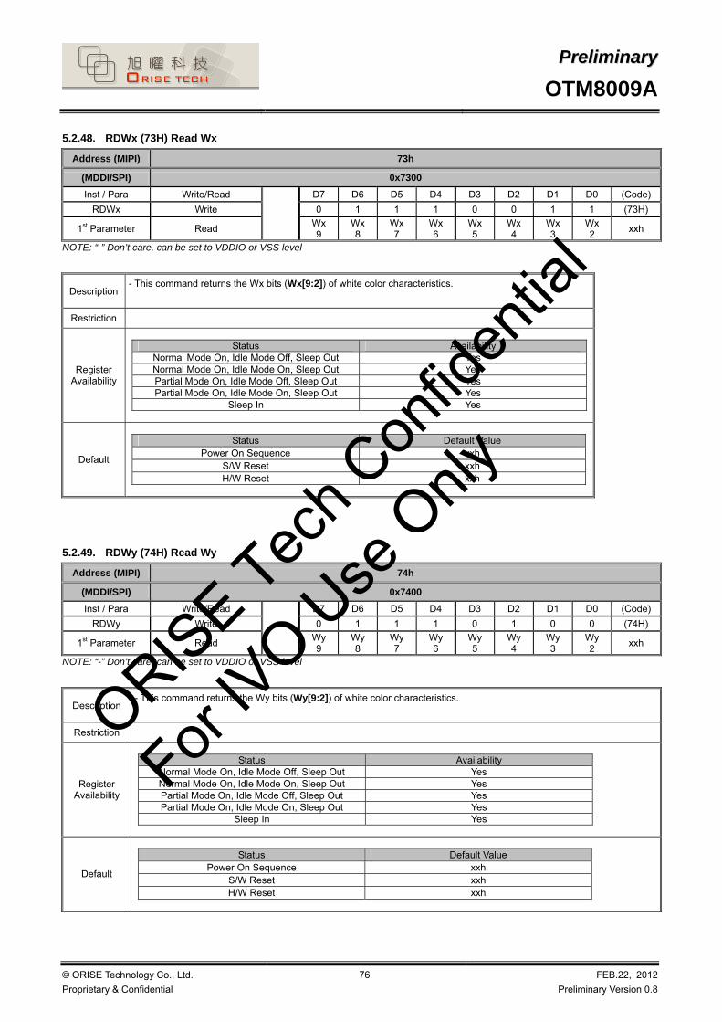
PPrreelliimmiinnaarryy
OTM8009A
© ORISE Technology Co., Ltd.
Proprietary & Confidential
76 FEB.22, 2012
Preliminary Version 0.8
5.2.48. RDWx (73H) Read Wx
Address (MIPI) 73h
(MDDI/SPI) 0x7300
Inst / Para Write/Read D7 D6 D5 D4 D3 D2 D1 D0 (Code)
RDWx Write 0 1 1 1 0 0 1 1 (73H)
1st Parameter Read
Wx 9
Wx 8
Wx 7
Wx 6
Wx 5
Wx 4
Wx 3
Wx 2
xxh
NOTE: “-” Don’t care, can be set to VDDIO or VSS level
Description - This command returns the Wx bits (Wx[9:2]) of white color characteristics.
Restriction
Register Availability
Status Availability
Normal Mode On, Idle Mode Off, Sleep Out Yes Normal Mode On, Idle Mode On, Sleep Out Yes Partial Mode On, Idle Mode Off, Sleep Out Yes Partial Mode On, Idle Mode On, Sleep Out Yes
Sleep In Yes
Default
Status Default Value
Power On Sequence xxh S/W Reset xxh H/W Reset xxh
5.2.49. RDWy (74H) Read Wy
Address (MIPI) 74h
(MDDI/SPI) 0x7400
Inst / Para Write/Read D7 D6 D5 D4 D3 D2 D1 D0 (Code)
RDWy Write 0 1 1 1 0 1 0 0 (74H)
1st Parameter Read
Wy 9
Wy 8
Wy 7
Wy 6
Wy 5
Wy 4
Wy 3
Wy 2
xxh
NOTE: “-” Don’t care, can be set to VDDIO or VSS level
Description - This command returns the Wy bits (Wy[9:2]) of white color characteristics.
Restriction
Register Availability
Status Availability
Normal Mode On, Idle Mode Off, Sleep Out Yes Normal Mode On, Idle Mode On, Sleep Out Yes Partial Mode On, Idle Mode Off, Sleep Out Yes Partial Mode On, Idle Mode On, Sleep Out Yes
Sleep In Yes
Default
Status Default Value
Power On Sequence xxh S/W Reset xxh H/W Reset xxh
ORISE Tec
h Con
fiden
tial
For IV
O Use
Only

PPrreelliimmiinnaarryy
OTM8009A
© ORISE Technology Co., Ltd.
Proprietary & Confidential
77 FEB.22, 2012
Preliminary Version 0.8
5.2.50. RDRGLB (75H) Read Red/Green Low Bits
Address (MIPI) 75h
(MDDI/SPI) 0x7500
Inst / Para Write/Read D7 D6 D5 D4 D3 D2 D1 D0 (Code)
RDRGLB Write 0 1 1 1 0 1 0 1 (75H)
1st Parameter Read
Rx 1
Rx 0
Ry 1
Ry 0
Gx 1
Gx 0
Gy 1
Gy 0
xxh
NOTE: “-” Don’t care, can be set to VDDIO or VSS level
Description
- This command returns the lowest bits of red and green color characteristics.
Red: Rx and Ry
Green: Gx and Gy
Restriction
Register Availability
Status Availability
Normal Mode On, Idle Mode Off, Sleep Out Yes Normal Mode On, Idle Mode On, Sleep Out Yes Partial Mode On, Idle Mode Off, Sleep Out Yes Partial Mode On, Idle Mode On, Sleep Out Yes
Sleep In Yes
Default
Status Default Value
Power On Sequence xxh S/W Reset xxh H/W Reset xxh
ORISE Tec
h Con
fiden
tial
For IV
O Use
Only

PPrreelliimmiinnaarryy
OTM8009A
© ORISE Technology Co., Ltd.
Proprietary & Confidential
78 FEB.22, 2012
Preliminary Version 0.8
5.2.51. RDRx (76H) Read Rx
Address (MIPI) 76h
(MDDI/SPI) 0x7600
Inst / Para Write/Read D7 D6 D5 D4 D3 D2 D1 D0 (Code)
RDRx Write 0 1 1 1 0 1 1 0 (76H)
1st Parameter Read
Rx 9
Rx 8
Rx 7
Rx 6
Rx 5
Rx 4
Rx 3
Rx 2
xxh
NOTE: “-” Don’t care, can be set to VDDIO or VSS level
Description - This command returns the Rx bits (Rx[9:2]) of red color characteristics.
Restriction
Register Availability
Status Availability
Normal Mode On, Idle Mode Off, Sleep Out Yes Normal Mode On, Idle Mode On, Sleep Out Yes Partial Mode On, Idle Mode Off, Sleep Out Yes Partial Mode On, Idle Mode On, Sleep Out Yes
Sleep In Yes
Default
Status Default Value
Power On Sequence xxh S/W Reset xxh H/W Reset xxh
5.2.52. RDRy (77H) Read Ry
Address (MIPI) 77h
(MDDI/SPI) 0x7700
Inst / Para Write/Read D7 D6 D5 D4 D3 D2 D1 D0 (Code)
RDRy Write 0 1 1 1 0 1 1 1 (77H)
1st Parameter Read
Ry 9
Ry 8
Ry 7
Ry 6
Ry 5
Ry 4
Ry 3
Ry 2
xxh
NOTE: “-” Don’t care, can be set to VDDIO or VSS level
Description - This command returns the Ry bits (Ry[9:2]) of red color characteristics.
Restriction
Register Availability
Status Availability
Normal Mode On, Idle Mode Off, Sleep Out Yes Normal Mode On, Idle Mode On, Sleep Out Yes Partial Mode On, Idle Mode Off, Sleep Out Yes Partial Mode On, Idle Mode On, Sleep Out Yes
Sleep In Yes
Default
Status Default Value
Power On Sequence xxh S/W Reset xxh H/W Reset xxh
ORISE Tec
h Con
fiden
tial
For IV
O Use
Only

PPrreelliimmiinnaarryy
OTM8009A
© ORISE Technology Co., Ltd.
Proprietary & Confidential
79 FEB.22, 2012
Preliminary Version 0.8
5.2.53. RDGx (78H) Read Gx
Address (MIPI) 78h
(MDDI/SPI) 0x7800
Inst / Para Write/Read D7 D6 D5 D4 D3 D2 D1 D0 (Code)
RDGx Write 0 1 1 1 1 0 0 0 (78H)
1st Parameter Read
Gx 9
Gx 8
Gx 7
Gx 6
Gx 5
Gx 4
Gx 3
Gx 2
xxh
NOTE: “-” Don’t care, can be set to VDDIO or VSS level
Description - This command returns the Gx bits (Gx[9:2]) of green color characteristics.
Restriction
Register Availability
Status Availability
Normal Mode On, Idle Mode Off, Sleep Out Yes Normal Mode On, Idle Mode On, Sleep Out Yes Partial Mode On, Idle Mode Off, Sleep Out Yes Partial Mode On, Idle Mode On, Sleep Out Yes
Sleep In Yes
Default
Status Default Value
Power On Sequence xxh S/W Reset xxh H/W Reset xxh
5.2.54. RDGy (79H) Read Gy
Address (MIPI) 79h
(MDDI/SPI) 0x7900
Inst / Para Write/Read D7 D6 D5 D4 D3 D2 D1 D0 (Code)
RDGy Write 0 1 1 1 1 0 0 1 (79H)
1st Parameter Read
Gy 9
Gy 8
Gy 7
Gy 6
Gy 5
Gy 4
Gy 3
Gy 2
xxh
NOTE: “-” Don’t care, can be set to VDDIO or VSS level
Description - This command returns the Gy bits (Gy[9:2]) of green color characteristics.
Restriction
Register Availability
Status Availability
Normal Mode On, Idle Mode Off, Sleep Out Yes Normal Mode On, Idle Mode On, Sleep Out Yes Partial Mode On, Idle Mode Off, Sleep Out Yes Partial Mode On, Idle Mode On, Sleep Out Yes
Sleep In Yes
Default
Status Default Value
Power On Sequence xxh S/W Reset xxh H/W Reset xxh
ORISE Tec
h Con
fiden
tial
For IV
O Use
Only

PPrreelliimmiinnaarryy
OTM8009A
© ORISE Technology Co., Ltd.
Proprietary & Confidential
80 FEB.22, 2012
Preliminary Version 0.8
5.2.55. RDBALB (7AH) Read Blue/AColour Low Bits
Address (MIPI) 7Ah
(MDDI/SPI) 0x7A00
Inst / Para Write/Read D7 D6 D5 D4 D3 D2 D1 D0 (Code)
RDBALB Write 0 1 1 1 1 0 1 0 (7AH)
1st Parameter Read
Bx 1
Bx 0
By 1
By 0
Ax 1
Ax 0
Ay 1
Ay 0
xxh
NOTE: “-” Don’t care, can be set to VDDIO or VSS level
Description
- This command returns the lowest bits of blue and A color characteristics.
Blue: Bx and By
A: Ax and Ay
- If A is not used Ax[1:0] and Ay[1:0] bits are set to ‘0’s.
Restriction
Register Availability
Status Availability
Normal Mode On, Idle Mode Off, Sleep Out Yes Normal Mode On, Idle Mode On, Sleep Out Yes Partial Mode On, Idle Mode Off, Sleep Out Yes Partial Mode On, Idle Mode On, Sleep Out Yes
Sleep In Yes
Default
Status Default Value
Power On Sequence xxh S/W Reset xxh H/W Reset xxh
ORISE Tec
h Con
fiden
tial
For IV
O Use
Only

PPrreelliimmiinnaarryy
OTM8009A
© ORISE Technology Co., Ltd.
Proprietary & Confidential
81 FEB.22, 2012
Preliminary Version 0.8
5.2.56. RDBx (7BH) Read Bx
Address (MIPI) 7Bh
(MDDI/SPI) 0x7B00
Inst / Para Write/Read D7 D6 D5 D4 D3 D2 D1 D0 (Code)
RDBx Write 0 1 1 1 1 0 1 1 (7BH)
1st Parameter Read
Bx 9
Bx 8
Bx 7
Bx 6
Bx 5
Bx 4
Bx 3
Bx 2
xxh
NOTE: “-” Don’t care, can be set to VDDIO or VSS level
Description - This command returns the Bx bits (Bx[9:2]) of blue color characteristics.
Restriction
Register Availability
Status Availability
Normal Mode On, Idle Mode Off, Sleep Out Yes Normal Mode On, Idle Mode On, Sleep Out Yes Partial Mode On, Idle Mode Off, Sleep Out Yes Partial Mode On, Idle Mode On, Sleep Out Yes
Sleep In Yes
Default
Status Default Value
Power On Sequence xxh S/W Reset xxh H/W Reset xxh
5.2.57. RDBy (7CH) Read By
Address (MIPI) 7Ch
(MDDI/SPI) 0x7C00
Inst / Para Write/Read D7 D6 D5 D4 D3 D2 D1 D0 (Code)
RDBy Write 0 1 1 1 1 1 0 0 (7CH)
1st Parameter Read
By 9
By 8
By 7
By 6
By 5
By 4
By 3
By 2
xxh
NOTE: “-” Don’t care, can be set to VDDIO or VSS level
Description - This command returns the By bits (By[9:2]) of blue color characteristics.
Restriction
Register Availability
Status Availability
Normal Mode On, Idle Mode Off, Sleep Out Yes Normal Mode On, Idle Mode On, Sleep Out Yes Partial Mode On, Idle Mode Off, Sleep Out Yes Partial Mode On, Idle Mode On, Sleep Out Yes
Sleep In Yes
Default
Status Default Value
Power On Sequence xxh S/W Reset xxh H/W Reset xxh
ORISE Tec
h Con
fiden
tial
For IV
O Use
Only

PPrreelliimmiinnaarryy
OTM8009A
© ORISE Technology Co., Ltd.
Proprietary & Confidential
82 FEB.22, 2012
Preliminary Version 0.8
5.2.58. RDAx (7DH) Read Ax
Address (MIPI) 7Dh
(MDDI/SPI) 0x7D00
Inst / Para Write/Read D7 D6 D5 D4 D3 D2 D1 D0 (Code)
RDAx Write 0 1 1 1 1 1 0 1 (7DH)
1st Parameter Read
Ax 9
Ax 8
Ax 7
Ax 6
Ax 5
Ax 4
Ax 3
Ax 2
xxh
NOTE: “-” Don’t care, can be set to VDDIO or VSS level
Description
- This command returns the Ax bits (Ax[9:2]) of A color characteristics.
- Ax[9:2] are set to ‘0’s if they are not used.
Restriction
Register Availability
Status Availability
Normal Mode On, Idle Mode Off, Sleep Out Yes Normal Mode On, Idle Mode On, Sleep Out Yes Partial Mode On, Idle Mode Off, Sleep Out Yes Partial Mode On, Idle Mode On, Sleep Out Yes
Sleep In Yes
Default
Status Default Value
Power On Sequence xxh S/W Reset xxh H/W Reset xxh
5.2.59. RDAy (7EH) Read Ay
Address (MIPI) 7Eh
(MDDI/SPI) 0x7E00
Inst / Para Write/Read D7 D6 D5 D4 D3 D2 D1 D0 (Code)
RDAy Write 0 1 1 1 1 1 1 0 (7EH)
1st Parameter Read
Ay 9
Ay 8
Ay 7
Ay 6
Ay 5
Ay 4
Ay 3
Ay 2
xxh
NOTE: “-” Don’t care, can be set to VDDIO or VSS level
Description
- This command returns the Ay bits (Ay[9:2]) of A color characteristics.
- Ay[9:2] are set to ‘0’s if they are not used.
Restriction
Register Availability
Status Availability
Normal Mode On, Idle Mode Off, Sleep Out Yes Normal Mode On, Idle Mode On, Sleep Out Yes Partial Mode On, Idle Mode Off, Sleep Out Yes Partial Mode On, Idle Mode On, Sleep Out Yes
Sleep In Yes
Default
Status Default Value
Power On Sequence xxh S/W Reset xxh H/W Reset xxh
ORISE Tec
h Con
fiden
tial
For IV
O Use
Only

PPrreelliimmiinnaarryy
OTM8009A
© ORISE Technology Co., Ltd.
Proprietary & Confidential
83 FEB.22, 2012
Preliminary Version 0.8
5.2.60. RDDDBSTR (A1H): Read DDB Start
Address (MIPI) A1h
(MDDI/SPI) 0xA100 ~ 0xA104
Inst / Para Write/Read D7 D6 D5 D4 D3 D2 D1 D0 (Code)
RDDDBSTR Write 1 0 1 0 0 0 0 1 (A1H)
1st Parameter Read ID41
15 ID4114
ID4113
ID4112
ID4111
ID41 10
ID41 9
ID418
01h
2nd Parameter Read ID41
7 ID41
6 ID41
5 ID41
4 ID41
3 ID41
2 ID41
1 ID41
0 8Bh
3rd Parameter Read ID42
15 ID4214
ID4213
ID4212
ID4211
ID42 10
ID42 9
ID428
80h
4th Parameter Read ID42
7 ID42
6 ID42
5 ID42
4 ID42
3 ID42
2 ID42
1 ID42
0 09h
5th Parameter Read
1 1 1 1 1 1 1 1 FFh
NOTE: “-” Don’t care, can be set to VDDIO or VSS level
Description
- The command reads identifying and descriptive information from the peripheral. This information is organized in the Device Descriptor Block(DDB) stored on the peripheral.
- The format of returned data is as follows:
Parameter 1: MSB byte of Supplier ID.
Parameter 2: LSB byte of Supplier ID.
Parameter 3: MSB byte of Display module ID.
Parameter 4: LSB byte of Display module ID.
Parameter 5: FFh
The read sequence can be interrupted by any command and it can be continued by A8H command.
Restriction
Register Availability
Status Availability
Normal Mode On, Idle Mode Off, Sleep Out Yes Normal Mode On, Idle Mode On, Sleep Out Yes Partial Mode On, Idle Mode Off, Sleep Out Yes Partial Mode On, Idle Mode On, Sleep Out Yes
Sleep In Yes
Default
Status Default Value
Power On Sequence XXh S/W Reset XXh H/W Reset XXh
ORISE Tec
h Con
fiden
tial
For IV
O Use
Only

PPrreelliimmiinnaarryy
OTM8009A
© ORISE Technology Co., Ltd.
Proprietary & Confidential
84 FEB.22, 2012
Preliminary Version 0.8
5.2.61. RDDDBCNT (A8H): Read DDB Continue
Address (MIPI) A8h
(MDDI/SPI) 0xA800 ~ 0xA804
Inst / Para Write/Read D7 D6 D5 D4 D3 D2 D1 D0 (Code)
RDDDBCNT Write 1 0 1 0 1 0 0 0 (A8H)
1st Parameter Read Idxx
nn Idxxnn
Idxxnn
Idxxnn
Idxxnn
Idxx nn
Idxx nn
Idxxnn
xxh
2nd Parameter Read Idxx
nn Idxxnn
Idxxnn
Idxxnn
Idxxnn
Idxx nn
Idxx nn
Idxxnn
xxh
.. Read - - - - - - - - xxh
Nth Parameter Read
Idxxnn
Idxxnn
Idxxnn
Idxxnn
Idxxnn
Idxx nn
Idxx nn
Idxxnn
xxh
NOTE: “-” Don’t care, can be set to VDDIO or VSS level
Description
- This command returns supplier’s identification and display module model/revision information from the point where RDDDBSTR command was interrupted by an other command.
- See more on A1H command.
Restriction
Register Availability
Status Availability
Normal Mode On, Idle Mode Off, Sleep Out Yes Normal Mode On, Idle Mode On, Sleep Out Yes Partial Mode On, Idle Mode Off, Sleep Out Yes Partial Mode On, Idle Mode On, Sleep Out Yes
Sleep In Yes
Default
Status Default Value
Power On Sequence XXh S/W Reset XXh H/W Reset XXh
ORISE Tec
h Con
fiden
tial
For IV
O Use
Only

PPrreelliimmiinnaarryy
OTM8009A
© ORISE Technology Co., Ltd.
Proprietary & Confidential
85 FEB.22, 2012
Preliminary Version 0.8
5.2.62. RDFCS (AAH): Read First Checksum
Address (MIPI) AAh
(MDDI/SPI) 0xAA00
Inst / Para Write/Read D7 D6 D5 D4 D3 D2 D1 D0 (Code)
RDFCS Write 1 0 1 0 1 0 1 0 (AAH)
1st Parameter Read
FCS
7 FCS
6 FCS
5 FCS
4 FCS
3 FCS
2 FCS
1 FCS
0 xxh
NOTE: “-” Don’t care, can be set to VDDIO or VSS level
Description - This command returns the first checksum what has been calculated from area registers and the frame memory after the
write access to those registers and/or frame memory has been done.
Restriction - It will be necessary to wait 150ms after there is the last write access on area registers before there can read this checksum value.
Register Availability
Status Availability
Normal Mode On, Idle Mode Off, Sleep Out Yes Normal Mode On, Idle Mode On, Sleep Out Yes Partial Mode On, Idle Mode Off, Sleep Out Yes Partial Mode On, Idle Mode On, Sleep Out Yes
Sleep In Yes
Default
Status Default Value
Power On Sequence 00h S/W Reset 00h H/W Reset 00h
ORISE Tec
h Con
fiden
tial
For IV
O Use
Only

PPrreelliimmiinnaarryy
OTM8009A
© ORISE Technology Co., Ltd.
Proprietary & Confidential
86 FEB.22, 2012
Preliminary Version 0.8
5.2.63. RDCCS (AFH): Read Continue Checksum
Address (MIPI) AFh
(MDDI/SPI) 0xAF00
Inst / Para Write/Read D7 D6 D5 D4 D3 D2 D1 D0 (Code)
RDCCS Write 1 0 1 0 1 1 1 1 (AFH)
1st Parameter Read
CCS
7 CCS
6 CCS
5 CCS
4 CCS
3 CCS
2 CCS
1 CCS
0 xxh
NOTE: “-” Don’t care, can be set to VDDIO or VSS level
Description
- This command returns the continue checksum what has been calculated continuously after the first checksum has calculated from area registers and the frame memory after the write access to those registers and/or frame memory has been done.
Restriction - It will be necessary to wait 300ms after there is the last write access on area registers before there can read this checksum value in the first time.
Register Availability
Status Availability
Normal Mode On, Idle Mode Off, Sleep Out Yes Normal Mode On, Idle Mode On, Sleep Out Yes Partial Mode On, Idle Mode Off, Sleep Out Yes Partial Mode On, Idle Mode On, Sleep Out Yes
Sleep In Yes
Default
Status Default Value
Power On Sequence 00h S/W Reset 00h H/W Reset 00h
5.2.64. RDID1 (DAH): Read ID1
Address (MIPI) DAh
(MDDI/SPI) 0xDA00
Inst / Para Write/Read D7 D6 D5 D4 D3 D2 D1 D0 (Code)
RDID1 Write 1 1 0 1 1 0 1 0 (DAH)
1st Parameter Read
ID1 7
ID1 6
ID1 5
ID1 4
ID1 3
ID1 2
ID1 1
ID1 0
40h
NOTE: “-” Don’t care, can be set to VDDIO or VSS level
Description - This read byte identifies the display module’s manufacturer.
Restriction - None
Register Availability
Status Availability
Normal Mode On, Idle Mode Off, Sleep Out Yes Normal Mode On, Idle Mode On, Sleep Out Yes Partial Mode On, Idle Mode Off, Sleep Out Yes Partial Mode On, Idle Mode On, Sleep Out Yes
Sleep In Yes
Default
Status Default Value
Power On Sequence 40h S/W Reset 40h H/W Reset 40h
ORISE Tec
h Con
fiden
tial
For IV
O Use
Only

PPrreelliimmiinnaarryy
OTM8009A
© ORISE Technology Co., Ltd.
Proprietary & Confidential
87 FEB.22, 2012
Preliminary Version 0.8
5.2.65. RDID2 (DBH): Read ID2
Address (MIPI) DBh
(MDDI/SPI) 0xDB00
Inst / Para Write/Read D7 D6 D5 D4 D3 D2 D1 D0 (Code)
RDID2 Write 1 1 0 1 1 0 1 1 (DBH)
1st Parameter Read
ID2 7
ID2 6
ID2 5
ID2 4
ID2 3
ID2 2
ID2 1
ID2 0
00h
NOTE: “-” Don’t care, can be set to VDDIO or VSS level
Description - This read byte is used to track the display module/driver version. It is defined by display supplier (with agreement) and
changes each time a revision is made to the display, material or construction specifications.
Restriction - None
Register Availability
Status Availability
Normal Mode On, Idle Mode Off, Sleep Out Yes Normal Mode On, Idle Mode On, Sleep Out Yes Partial Mode On, Idle Mode Off, Sleep Out Yes Partial Mode On, Idle Mode On, Sleep Out Yes
Sleep In Yes
Default
Status Default Value
Power On Sequence 00h S/W Reset 00h H/W Reset 00h
5.2.66. RDID3 (DCH): Read ID3
Address (MIPI) DCh
(MDDI/SPI) 0xDC00
Inst / Para Write/Read D7 D6 D5 D4 D3 D2 D1 D0 (Code)
RDID3 Write 1 1 0 1 1 1 0 0 (DCH)
1st Parameter Read
ID3 7
ID3 6
ID3 5
ID3 4
ID3 3
ID3 2
ID3 1
ID3 0
00h
NOTE: “-” Don’t care, can be set to VDDIO or VSS level
Description - This read byte identifies the display module/driver.
Restriction - None
Register Availabili
ty
Status Availability
Normal Mode On, Idle Mode Off, Sleep Out Yes Normal Mode On, Idle Mode On, Sleep Out Yes Partial Mode On, Idle Mode Off, Sleep Out Yes Partial Mode On, Idle Mode On, Sleep Out Yes
Sleep In Yes
Default
Status Default Value
Power On Sequence 00h S/W Reset 00h H/W Reset 00h
ORISE Tec
h Con
fiden
tial
For IV
O Use
Only

PPrreelliimmiinnaarryy
OTM8009A
© ORISE Technology Co., Ltd.
Proprietary & Confidential
88 FEB.22, 2012
Preliminary Version 0.8
5.3. Customer Command List and Description (Manufacturer Command Set / Command 2)
(1) MIPI IF Enable access command 2 registers:
(2) Other IF Enable access command 2 registers:
Write Register 0x00h with parameter 0x80h
Write Register 0xFFh with parameter 0x80h + 0x09h + 0x01h
Write Register 0xFFh with parameter 0x80h + 0x09h
Write Register 0xFF00h with parameter 0x0080h
Write Register 0xFF01h with parameter 0x0009h
Write Register 0xFF02h with parameter 0x0001h
Write Register 0xFF80h with parameter 0x0080h
Write Register 0xFF81h with parameter 0x0009h
ORISE Tec
h Con
fiden
tial
For IV
O Use
Only

PPrreelliimmiinnaarryy
OTM8009A
© ORISE Technology Co., Ltd.
Proprietary & Confidential
89 FEB.22, 2012
Preliminary Version 0.8
5.3.1. ADRSFT (0000h): Address Shift Function
Address 00h
Address (SPI/I2C/MDDI)
0000h (0x01st parameter)
Inst. / Para. Write/Read D[15:8] D7 D6 D5 D4 D3 D2 D1 D0 Default
Instruction Write 00h 0 0 0 0 0 0 0 0
Parameter Write SFT7 SFT6 SFT5 SFT4 SFT3 SFT2 SFT1 SFT0 00h
Description
- Address shift function can be enable when EXTC=1. (EXTC bit at $FF00h)
- SFT[7:0] can define the parameter counter number of command 2 register
Restriction
Default
Status Default Value
OTP un-programmed No OTP Support OTP Programmed No OTP Support
ORISE Tec
h Con
fiden
tial
For IV
O Use
Only

PPrreelliimmiinnaarryy
OTM8009A
© ORISE Technology Co., Ltd.
Proprietary & Confidential
90 FEB.22, 2012
Preliminary Version 0.8
5.3.2. CMD2_ENA1 (FF00h): Enable Access Command 2 & Software EXTC Enable
Address FFh
Address (SPI/I2C/MDDI)
FF00h ~ FF02h (0x01st ~ 0x03rd parameter)
Inst. / Para. Write/Read D[15:8] D7 D6 D5 D4 D3 D2 D1 D0 Default
Instruction Write 00h 1 1 1 1 1 1 1 1
1st Parameter Write PW15 PW14 PW13 PW12 PW11 PW10 PW9 PW8 00h
2nd Parameter Write PW7 PW6 PW5 PW4 PW3 PW2 PW1 PW0 00h
3rd Parameter Write 0 0 0 0 0 0 0 EXTC 00h
Description
- To enter in Command 2 Mode, please let PW[15:8] = 80h and PW[7:0] = 09h
- To enable write function of Command 2 & enable parameter shift function, please let EXTC = 1h.
Restriction
Default
Status Default Value
OTP un-programmed No OTP Support OTP Programmed No OTP Support
5.3.3. CMD2_ENA2 (FF80h): Enable Access Orise Command 2
Address FFh
Address (SPI/I2C/MDDI)
FF80h ~ FF81h (0x81sh ~ 0x82th parameter)
Inst. / Para. Write/Read D[15:8] D7 D6 D5 D4 D3 D2 D1 D0 Default
Instruction Write 00h 1 1 1 1 1 1 1 1
129th Parameter Write OPW15 OPW14 OPW13 OPW12 OPW11 OPW10 OPW9 OPW8 00h
130th Parameter Write OPW7 OPW6 OPW5 OPW4 OPW3 OPW2 OPW1 OPW0 00h
Description
- To enter in Orise Command 2 Mode, please let OPW[15:8] = 80h and OPW[7:0] = 09h
- To enable write function of Command 2 & enable parameter shift function, please let EXTC = 1h.
Restriction - Read and Write, Only access when CMD2 mode enable.
Default
Status Default Value
OTP un-programmed No OTP Support OTP Programmed No OTP Support
ORISE Tec
h Con
fiden
tial
For IV
O Use
Only

PPrreelliimmiinnaarryy
OTM8009A
© ORISE Technology Co., Ltd.
Proprietary & Confidential
91 FEB.22, 2012
Preliminary Version 0.8
5.3.4. OTPSEL (A000h): Gamma 2.2 OTP Select Region
Address A0h
Address (SPI/I2C/MDDI)
A000h (0x01st parameter)
Inst. / Para. Write/Read D[15:8] D7 D6 D5 D4 D3 D2 D1 D0 Default
Instruction Write 00h 1 0 1 0 0 0 0 0 A0h
Parameter Write/Read 0 0 0 0 0 0 0 reg_gma_otp_s
el 00h
Description
Select Gamma 2.2 OTP Region
0:Select Gamma 2.2 OTP Area 1 to program
1:Select Gamma 2.2 OTP Area 2 to program
Restriction - Read and Write, Only access when Orise mode enable.
Default
Status Default Value
OTP un-programmed Set as default value OTP Programmed Set as OTP value
ORISE Tec
h Con
fiden
tial
For IV
O Use
Only
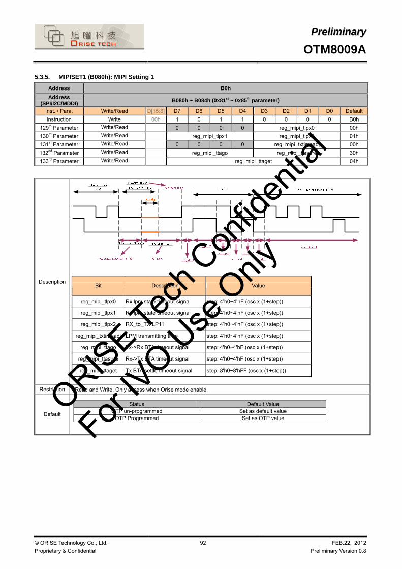
PPrreelliimmiinnaarryy
OTM8009A
© ORISE Technology Co., Ltd.
Proprietary & Confidential
92 FEB.22, 2012
Preliminary Version 0.8
5.3.5. MIPISET1 (B080h): MIPI Setting 1
Address B0h
Address (SPI/I2C/MDDI)
B080h ~ B084h (0x81st ~ 0x85th parameter)
Inst. / Para. Write/Read D[15:8] D7 D6 D5 D4 D3 D2 D1 D0 Default
Instruction Write 00h 1 0 1 1 0 0 0 0 B0h
129th Parameter Write/Read 0 0 0 0 reg_mipi_tlpx0 00h
130th Parameter Write/Read reg_mipi_tlpx1 reg_mipi_tlpx2 01h
131st Parameter Write/Read 0 0 0 0 reg_mipi_txtimeadj 00h
132nd Parameter Write/Read reg_mipi_ttago reg_mipi_ttasure 30h
133rd Parameter Write/Read reg_mipi_ttaget 04h
Description
Bit Description Value
reg_mipi_tlpx0 Rx lpm state timeout signal step: 4’h0~4’hF (osc x (1+step))
reg_mipi_tlpx1 Rx lpm state timeout signal step: 4’h0~4’hF (osc x (1+step))
reg_mipi_tlpx2 RX_to_TX LP11 step: 4’h0~4’hF (osc x (1+step))
reg_mipi_txtimeadj LPM transmitting time step: 4’h0~4’hF (osc x (1+step))
reg_mipi_ttago Tx->Rx BTA timeout signal step: 4'h0~4'hF (osc x (1+step))
reg_mipi_ttasure Rx->Tx BTA timeout signal step: 4'h0~4'hF (osc x (1+step))
reg_mipi_ttaget Tx BTA settle timeout signal step: 8'h0~8'hFF (osc x (1+step))
Restriction - Read and Write, Only access when Orise mode enable.
Default
Status Default Value
OTP un-programmed Set as default value OTP Programmed Set as OTP value
ORISE Tec
h Con
fiden
tial
For IV
O Use
Only

PPrreelliimmiinnaarryy
OTM8009A
© ORISE Technology Co., Ltd.
Proprietary & Confidential
93 FEB.22, 2012
Preliminary Version 0.8
5.3.6. MIPISET2 (B0B2h): MIPI Setting 2
Address B0h
Address (SPI/I2C/MDDI)
B0B2h ~ B0B4h (0xB3rd ~ 0xB5th parameter)
Inst. / Para. Write/Read D[15:8] D7 D6 D5 D4 D3 D2 D1 D0 Default
Instruction Write 00h 1 0 1 1 0 0 0 0 B0h
179th Parameter Write/Read 0 0 reg_mipi_mp_clk_dly_sel 06h
180th Parameter Write/Read 0 0 reg_mipi_mp_ch0_dly_sel 00h
181st Parameter Write/Read 0 0 reg_mipi_mp_ch1_dly_sel 00h
Description
Bit Description Value
reg_mipi_mp_clk_dly_sel MIPI Clock Lane Delay 1step = 30pS reg_mipi_mp_ch0_dly_sel MIPI D0 Lane Delay 1step = 30pS reg_mipi_mp_ch1_dly_sel MIPI D1 Lane Delay 1step = 30pS
Restriction - Read and Write, Only access when Orise mode enable.
Default
Status Default Value
OTP un-programmed Set as default value OTP Programmed Set as OTP value
ORISE Tec
h Con
fiden
tial
For IV
O Use
Only

PPrreelliimmiinnaarryy
OTM8009A
© ORISE Technology Co., Ltd.
Proprietary & Confidential
94 FEB.22, 2012
Preliminary Version 0.8
5.3.7. IF_PARA1 (B280H) IF Parameter 1
Address B2h
Address (SPI/I2C/MDDI)
B280h (0x81st parameter)
Inst. / Para. Write/Read D[15:8] D7 D6 D5 D4 D3 D2 D1 D0 Default
Instruction Write 00h 1 0 1 1 0 0 1 0 B2h
129’th Parameter Write/Read 0 0 1 0 0 LUT_IP
M[2] LUT_IP
M[1] LUT_IP
M[0]24h
Description
- LUT_IPM[2:0] : This register is used to expand data selection in 16bit mode and 18bit mode.
Data expansion table in case of Green of 16bit Mode and 18bit Mode.
IPM R[7] R[6] R[5] R[4] R[3] R[2] R[1] R[0]
0 D[5] D[4] D[3] D[2] D[1] D[0] 0 0
1 D[5] D[4] D[3] D[2] D[1] D[0] 0 1
2 D[5] D[4] D[3] D[2] D[1] D[0] 1 0
3 D[5] D[4] D[3] D[2] D[1] D[0] 1 1
4 D[5] D[4] D[3] D[2] D[1] D[0] D[5] D[4] default
5 D[5] D[4] D[3] D[2] D[1] D[0] D[5] 0
6 D[5] D[4] D[3] D[2] D[1] D[0] D[5] 1
7 D[5] D[4] D[3] D[2] D[1] D[0] 0 0
Data expansion table in case of Red and Blue of 16bit Mode.
IPM R[7] R[6] R[5] R[4] R[3] R[2] R[1] R[0]
0 D[4] D[3] D[2] D[1] D[0] D[4] 0 0
1 D[4] D[3] D[2] D[1] D[0] D[4] 0 1
2 D[4] D[3] D[2] D[1] D[0] D[4] 1 0
3 D[4] D[3] D[2] D[1] D[0] D[4] 1 1
4 D[4] D[3] D[2] D[1] D[0] D[4] D[3] D[2] default
5 D[4] D[3] D[2] D[1] D[0] D[4] D[4] 0
6 D[4] D[3] D[2] D[1] D[0] D[4] D[4] 1
7 D[4] D[3] D[2] D[1] D[0] D[4] 0 0
Restriction - Read and Write, Only access when Orise mode enable.
Default
Status Default Value
OTP un-programmed Set as default value OTP Programmed Set as OTP value
ORISE Tec
h Con
fiden
tial
For IV
O Use
Only

PPrreelliimmiinnaarryy
OTM8009A
© ORISE Technology Co., Ltd.
Proprietary & Confidential
95 FEB.22, 2012
Preliminary Version 0.8
5.3.8. IF_PARA2 (B282H) IF Parameter 2
Address B2h
Address (SPI/I2C/MDDI)
B282h (0x83st parameter)
Inst. / Para. Write/Read D[15:8] D7 D6 D5 D4 D3 D2 D1 D0 Default
Instruction Write 00h 1 0 1 1 0 0 1 0
131’th Parameter Write/Read RGB_V
SP RGB_H
SP RGB_D
P RGB_E
P 0 0
RGB_updata_freq[1]
RGB_updata_freq[0]
00h
Description
- This command is used to set RGB IF Function.
Symbol Name Clock polarity set for RGB Interface
REG_VSP Vsync polarity set ‘1’ = High level sync clock ‘0’ = Low level sync clock
REG_HSP Hsync polarity set ‘1’ = High level sync clock ‘0’ = Low level sync clock
REG_DP PCLK polarity set ‘1’ = data fetched at the falling edge ‘0’ = data fetched at the rising edge
REG_EP Enable polarity set ‘1’ = Low enable for RGB interface ‘0’ = High enable for RGB interface
REG_VSP
0
1
REG_VSP=0
VSVS_int
0
1
REG_VSP=1
VSVS_int
REG_HSP
0
1
REG_HSP=0
HSHS_int
0
1
REG_HSP=1
HSHS_int
REG_DP
0
1
REG_DP=0
PCLKPCLK_int
0
1
REG_DP=1
PCLKPCLK_int
ORISE Tec
h Con
fiden
tial
For IV
O Use
Only

PPrreelliimmiinnaarryy
OTM8009A
© ORISE Technology Co., Ltd.
Proprietary & Confidential
96 FEB.22, 2012
Preliminary Version 0.8
REG_EP
0
1
REG_EP=0
DEDE_int
0
1
REG_EP=1
DEDE_int
-When RGB_VSP=0 ; RGB_HSP=0 ; RGB_DP=0 ; RGB_EP=0
- RGB_UPDATA_FREQ[1:0] : User could set frequency of RAM update from interface.
RGB_UPDAT_FREQ[1:0]Frequency(Frame)
00 1
01 2
10 3
11 4
Restriction - Read and Write, Only access when Orise mode enable.
ORISE Tec
h Con
fiden
tial
For IV
O Use
Only

PPrreelliimmiinnaarryy
OTM8009A
© ORISE Technology Co., Ltd.
Proprietary & Confidential
97 FEB.22, 2012
Preliminary Version 0.8
Default
Status Default Value
OTP un-programmed Set as default value OTP Programmed Set as OTP value
ORISE Tec
h Con
fiden
tial
For IV
O Use
Only

PPrreelliimmiinnaarryy
OTM8009A
© ORISE Technology Co., Ltd.
Proprietary & Confidential
98 FEB.22, 2012
Preliminary Version 0.8
5.3.9. PAD_PARA (B390H) IOPAD Parameter
Address B3h
Address (SPI/I2C/MDDI)
B390h ~ B392(0x91st ~ 0x93rd parameter)
Inst. / Para. Write/Read D[15:8] D7 D6 D5 D4 D3 D2 D1 D0 Default
Instruction Write 00h 1 0 1 1 0 0 1 1
145’th Parameter Write/Read SW_IM[3]
SW_IM[2]
SW_IM[1]
SW_IM[0]
0 SW_GM
[2] SW_GM
[1] SW_GM
[0] 00h
146’th Parameter Write/Read SW_SMX
SW_SMY
SW_SRGB
0 0 0 SW_I2C_SA[1]
SW_I2C_SA[0] 00h
147’th Parameter Write/Read SW_EXPEN[3]
SW_EXPEN[2]
SW_EXPEN[1]
SW_EXPEN[0]
0 1 0 1 05h
Description
- These registers are used to replace the Hardware PIN. Use SW_EXPEN[3:0] to enable Software control.
- SW_IM[3:0] : When SW_EXPEN[3] = 1 , this setting replace the Hardware PIN IM. SW_EXPEN[3] Interface Select
0 Pin_IM[3:0] 1 SW_IM[3:0]
- SW_GM[2:0] : When SW_EXPEN[2] = 1 , this setting is valid. SW_EXPEN[2] Resolution
0 480 x 800 1 SW_GM[2:0]
SW_GM[2:0] Resolution SW_GM[2:0] Resolution
000 480 x 800 100 480 x 720 001 480 x 864 101 480 x 640
010 480 x 854 110 480 x 480
011 480 x 800 111 480 x 360 - SW_SMX/SW_SMY/SW_SRGB/SW_I2C_SA[1:0]
Bit Description Value
SW_SMX Row address order
0 : Write/Read RAM Direction from Left to Right 1 : Write/Read RAM Direction from Right to Left ※ The fucnction only can be applied when SW_EXPEN[1] = 1. If SW_EXPEN[1] = 0, The Write/Read RAM Direction is Left to Rgiht.
SW_SMY Column address order
0 : Write/Read RAM Direction from Up to Down 1 : Write/Read RAM Direction from Down to Up ※ The fucnction only can be applied when SW_EXPEN[1] = 1. If SW_EXPEN[1] = 0, The Write/Read RAM Direction is Up to Down.
SW_SRGB RGB-BGR Order
0 : For RGB filter panel 1 : For BGR filter panel ※ The fucnction only can be applied when SW_EXPEN[1] = 1. If SW_EXPEN[1] = 0, The order is RGB.
SW_I2C_SA[1:0] Slave address at I2C I/F
00 : 1001100 01 : 1001101 10 : 1001100 11 : 1001101 ※ The fucnction only can be applied when SW_EXPEN[0] = 1.
Restriction - Read and Write, Only access when Orise mode enable.
Default
Status Default Value
OTP un-programmed Set as default value OTP Programmed Set as OTP value
ORISE Tec
h Con
fiden
tial
For IV
O Use
Only

PPrreelliimmiinnaarryy
OTM8009A
© ORISE Technology Co., Ltd.
Proprietary & Confidential
99 FEB.22, 2012
Preliminary Version 0.8
5.3.10. PANSET (B3A6h): Panel Type Setting
Address B3h
Address (SPI/I2C/MDDI)
B3A6h ~B3A7h (0xA7th ~0xA8th parameter)
Inst. / Para. Write/Read D[15:8] D7 D6 D5 D4 D3 D2 D1 D0 Default
Instruction Write 00h 1 0 1 1 0 0 1 1
167th Parameter Write/Read 0 0 1 0 ZIG_ SET
1 1 1 2Fh
168th Parameter Write/Read 0 0 0 0 0 0 0 ZIG_ OPT
00h
Description
- These registers are used to control panel type
ZIGOPT ZIGSET Panel Type
0 X Normal Panel
0 Normal Panel 1
1 Pseudo-dot Panel
X: Don’t care
Restriction - Read and Write, Only access when Orise mode enable.
Default
Status Default Value
OTP un-programmed Set as default value OTP Programmed Set as OTP value
ORISE Tec
h Con
fiden
tial
For IV
O Use
Only

PPrreelliimmiinnaarryy
OTM8009A
© ORISE Technology Co., Ltd.
Proprietary & Confidential
100 FEB.22, 2012
Preliminary Version 0.8
5.3.11. RAMPWRSET (B3C0h): SRAM Power Setting
Address B3h
Address (SPI/I2C/MDDI)
B3C0h ~B3C1h (0xC1st ~0xC2rd parameter)
Inst. / Para. Write/Read D[15:8] D7 D6 D5 D4 D3 D2 D1 D0 Default
Instruction Write 00h 1 0 1 1 0 0 1 1
193rd Parameter Write/Read 0 0 0 RAMOFF[1:0] RAMOFF_TEST[2:0] 09h
194th Parameter Write/Read rampwron_mdd
i_spi
rampwron_mdd
i_i2c0
rampwron_mipi
0 rampwron_rgb
0 rampwron_cpu
00h
Description
Note: X = Don’t care
Bit Description Value
RAMOFF[1:0] Turn off SRAM power condition
2'b00:Turn off SRAM power only when reset keeps low 2'b01:Turn off SRAM power when reset keeps low or Ultra Low Power Mode in sleep-in 2'b10:Turn off SRAM power when reset keeps low or sleep-in
RAMOFF_TEST[2:0] SRAM power test mode. Orsie use only
3’b001
rampwron_mddi_spi Force turn on SRAM power during mddi_spi IF mode
1: Turn on SRAM power during sleep in mode when IM = 0110 and 1110 0: Refer to RAMOFF[1:0]
rampwron_mddi_i2c Force turn on SRAM power during mddi_i2c mode
1: Turn on SRAM power during sleep in mode when IM = X111 0: Refer to RAMOFF[1:0]
rampwron_mipi Force turn on SRAM power during mipi IF mode
1: Turn on SRAM power during sleep in mode when IM = X101 0: Refer to RAMOFF[1:0]
rampwron_rgb Force turn on SRAM power during rgb IF mode
1: Turn on SRAM power during sleep in mode when IM = X011, X100 0: Refer to RAMOFF[1:0]
rampwron_cpu Force turn on SRAM power during cpu IF mode
1: Turn on SRAM power during sleep in mode when IM = X000, X001 and X010 0: Refer to RAMOFF[1:0]
Restriction - Read and Write, Only access when Orise mode enable.
Default
Status Default Value
OTP un-programmed Set as default value OTP Programmed Set as OTP value
ORIS
E Tech C
onfid
entia
l
For IV
O Use
Only

PPrreelliimmiinnaarryy
OTM8009A
© ORISE Technology Co., Ltd.
Proprietary & Confidential
101 FEB.22, 2012
Preliminary Version 0.8
5.3.12. TSP1(C080h) TCON Setting Parameter 1
Address C0h
Address (SPI/I2C/MDDI)
C080h ~ C088h (0x81st ~ 0x89th parameter)
Inst. / Para. Write/Read D[15:8] D7 D6 D5 D4 D3 D2 D1 D0 Default
Instruction Write 00h 1 1 0 0 0 0 0 0 C0h
129th Parameter Write/Read rtn[15] rtn[14] rtn[13] rtn[12] rtn[11] rtn[10] rtn[9] rtn[8] 00h
130th Parameter Write/Read rtn[7] rtn[6] rtn[5] rtn[4] rtn[3] rtn[2] rtn[1] rtn[0] 5Fh
131st Parameter Write/Read vfp[15] vfp[14] vfp[13] vfp[12] vfp[11] vfp[10] vfp[9] vfp[8] 00h
132nd Parameter Write/Read vfp[7] vfp[6] vfp[5] vfp[4] vfp[3] vfp[2] vfp[1] vfp[0] 10h
133rd Parameter Write/Read vbp[7] vbp[6] vbp[5] vbp[4] vbp[3] vbp[2] vbp[1] vbp[0] 10h
134th Parameter Write/Read pwrseq_rtn[15]
pwrseq_rtn[14]
pwrseq_rtn[13]
pwrseq_rtn[12]
pwrseq_rtn[11]
pwrseq_rtn[10]
pwrseq_rtn[9]
pwrseq_rtn[8]
00h
135th Parameter Write/Read pwrseq_rtn[7]
pwrseq_rtn[6]
pwrseq_rtn[5]
pwrseq_rtn[4]
pwrseq_rtn[3]
pwrseq_rtn[2]
pwrseq_rtn[1]
pwrseq_rtn[0]
5Fh
136th Parameter Write/Read pwrseq_vfp[7]
pwrseq_vfp[6]
pwrseq_vfp[5]
pwrseq_vfp[4]
pwrseq_vfp[3]
pwrseq_vfp[2]
pwrseq_vfp1]
pwrseq_vfp[0]
10h
137th Parameter Write/Read pwrseq_vbp[7]
pwrseq_vbp[6]
pwrseq_vbp[5]
pwrseq_vbp[4]
pwrseq_vbp[3]
pwrseq_vbp[2]
pwrseq_vbp[1]
pwrseq_vbp[0]
10h
Description
- RTN is used to set the cycles of mclk for one line.
- VFP is used to set Vertical front porch ; VBP is used to set Vertical back porch.
- 129th ~ 133rd parameters are used during normal display period; 134th ~ 137th parameters are used for power–on sequence period.
Restriction - Read and Write, Only access when Orise mode enable.
Default
Status Default Value
OTP un-programmed Set as default value OTP Programmed Set as OTP value
ORISE Tec
h Con
fiden
tial
For IV
O Use
Only

PPrreelliimmiinnaarryy
OTM8009A
© ORISE Technology Co., Ltd.
Proprietary & Confidential
102 FEB.22, 2012
Preliminary Version 0.8
5.3.13. PTSP1(C092h) Panel Timing Setting Parameter 1
Address C0h
Address (SPI/I2C/MDDI)
C092h ~ C093h ( 0x93st ~ 0x94nd parameter )
Inst. / Para. Write/Read D[15:8] D7 D6 D5 D4 D3 D2 D1 D0 Default
Instruction Write 00h 1 1 0 0 0 0 0 0 C0h
147th Parameter Write/Read mck_shift2[15]
mck_shift2[14]
mck_shift2[13]
mck_shift2[12]
mck_shift2[11]
mck_ shift2[10]
mck_ shift2[9]
mck_shift2[8] 00h
148th Parameter Write/Read mck_shift2[7]
mck_shift2[6]
mck_shift2[5]
mck_shift2[4]
mck_shift2[3]
mck_ shift2[2]
mck_ shift2[1]
mck_shift2[0] 10h
Description
- mck_shift2 is used to control the hold timing of source output
Gate signal
Source output
mck_shift2
SD_PLSD_PC
HSD_OP
SD_DAC
mck_shift2[15:0] time unit (mclk) 0000h 1 0001h 2 0002h 3
… … FFFFh 65536
- For SD_PL/SD_PCH/SD_OP/SD_DAC, please refer to SD_CTRL(C0A1h)
Restriction - Read and Write, Only access when Orise mode enable.
Default
Status Default Value
OTP un-programmed Set as default value OTP Programmed Set as OTP value
ORISE Tec
h Con
fiden
tial
For IV
O Use
Only

PPrreelliimmiinnaarryy
OTM8009A
© ORISE Technology Co., Ltd.
Proprietary & Confidential
103 FEB.22, 2012
Preliminary Version 0.8
5.3.14. PTSP2 (C094h) Panel Timing Setting Parameter 2
Address C0h
Address (SPI/I2C/MDDI)
C094h ~ C095h ( 0x95st ~ 0x96nd parameter )
Inst. / Para. Write/Read D[15:8] D7 D6 D5 D4 D3 D2 D1 D0 Default
Instruction Write 00h 1 1 0 0 0 0 0 0 C0h
149th Parameter Write/Read mck_shift3[15]
mck_shift3[14]
mck_shift3[13]
mck_shift3[12]
mck_shift3[11]
mck_ shift3[10]
mck_ shift3[9]
mck_shift3[8] 00h
150th Parameter Write/Read mck_shift3[7]
mck_shift3[6]
mck_shift3[5]
mck_shift3[4]
mck_shift3[3]
mck_ shift3[2]
mck_ shift3[1]
mck_shift3[0] 13h
Description
- mck_shift3 is used to control the loda location for latch control
- The difference between mck_shift2 and mck_shift3 must keep three.
mck_shift2[15:0] time unit (mclk) 0000h 1 0001h 2 0002h 3
… … FFFFh 65536
-
Restriction - Read and Write, Only access when Orise mode enable.
Default
Status Default Value
OTP un-programmed Set as default value OTP Programmed Set as OTP value
ORISE Tec
h Con
fiden
tial
For IV
O Use
Only

PPrreelliimmiinnaarryy
OTM8009A
© ORISE Technology Co., Ltd.
Proprietary & Confidential
104 FEB.22, 2012
Preliminary Version 0.8
5.3.15. SD_CTRL (C0A2h) Source Driver Timing Setting
Address C0h
Address (SPI/I2C/MDDI)
C0A2h ~C0A7h (0xA3rd ~ 0xA8th parameter)
Inst. / Para. Write/Read D[15:8] D7 D6 D5 D4 D3 D2 D1 D0 Default
Instruction Write 00h 1 1 0 0 0 0 0 0 C0h
163rd Parameter Write/Read SD_PL[7]
SD_PL[6]
SD_PL[5]
SD_PL[4]
SD_PL[3]
SD_PL [2]
SD_PL [1]
SD_PL[0] 0Dh
164th Parameter Write/Read SD_PCH1[7]
SD_PCH1[6]
SD_PCH1[5]
SD_PCH1[4]
SD_PCH1[3]
SD_PCH1 [2]
SD_PCH1 [1]
SD_PCH1[0] 06h
165th Parameter Write/Read SD_PCH2[7]
SD_PCH2[6]
SD_PCH2[5]
SD_PCH2[4]
SD_PCH2[3]
SD_PCH2 [2]
SD_PCH2 [1]
SD_PCH2[0] 02h
166th Parameter Write/Read SD_OP1[7]
SD_OP1[6]
SD_OP1[5]
SD_OP1[4]
SD_OP1[3]
SD_OP1 [2]
SD_OP1 [1]
SD_OP1[0] 01h
167th Parameter Write/Read SD_OP2[7]
SD_OP2[6]
SD_OP2[5]
SD_OP2[4]
SD_OP2[3]
SD_OP2 [2]
SD_OP2 [1]
SD_OP2[0] 3Ch
168th Parameter Write/Read SD_OP3[7]
SD_OP3[6]
SD_OP3[5]
SD_OP3[4]
SD_OP3[3]
SD_OP3 [2]
SD_OP3 [1]
SD_OP3[0] 08h
Description
- - This command is used for source driver timing control.
- SD_PL: Source Driver Pull Low Timing. Set by (SD_PL[7:0] + 1) MCLK
- SD_PCH: Source Driver Pre-charge Timing. Set by (SD_PCH1[7:0] + SD_PCH2[7:0] + 2 ) MCLK
- SD_OP: Source Driver OP ON Timing. Set by (SD_OP1[7:0] + SD_OP2[7:0] + SD_OP3[7:0] + 3 )MCLK
- SD_DAC: Source Floating State: Set by (RTN - SD_PL - SD_PCH - SD_OP -5 )MCLK
Hsync
SD_PL
SD_PCH
SD_OP
SD_DAC
(SD_PL +1)
(SD_PCH1+SD_PCH2+2
(SD_OP1+SD_OP2+SD_OP3 +3)
1H (RTN+1)
Restriction - Read and Write, Only access when Orise mode enable.
Default
Status Default Value
OTP un-programmed Set as default value OTP Programmed Set as OTP value
ORISE Tec
h Con
fiden
tial
For IV
O Use
Only

PPrreelliimmiinnaarryy
OTM8009A
© ORISE Technology Co., Ltd.
Proprietary & Confidential
105 FEB.22, 2012
Preliminary Version 0.8
5.3.16. P_DRV_M(C0B4h) : Panel Driving Mode
Address C0h
Address (SPI/I2C/MDDI)
C0B4h (0xB5th parameter)
Inst. / Para. Write/Read D[15:8] D7 D6 D5 D4 D3 D2 D1 D0 Default
Instruction Write 00h 1 1 0 0 0 0 0 0 C0h
181st Parameter Write/Read 0 INV_MODE[2]
INV_MODE[1]
INV_MODE[0]
0 INV_MODE_IDLE[2]
INV_MODE_IDLE[1]
INV_MODE_IDLE[0]
00h
Description
- This command is used to set the inversion type and mode
181th Parameter Value Inversion Mode Selection 000 1 Dot Inversion 001 1+2 Dot Inversion 101 Column Inversion
INV_MODE[[2:0] (Normal Mode)
Others Reserved 000 1 Dot Inversion 001 1+2 Dot Inversion 101 Column Inversion
INV_MODE_IDLE[[2:0] (IDLE Mode)
Others Reserved
Restriction - Read and Write, Only access when Orise mode enable.
Default
Status Default Value
OTP un-programmed Set as default value OTP Programmed Set as OTP value
ORISE Tec
h Con
fiden
tial
For IV
O Use
Only

PPrreelliimmiinnaarryy
OTM8009A
© ORISE Technology Co., Ltd.
Proprietary & Confidential
106 FEB.22, 2012
Preliminary Version 0.8
5.3.17. OSC_ADJ(C181h) : Oscillator Adjustment for Idle/Normal Mode
Address C1h
Address (SPI/I2C/MDDI)
C181h (0x82nd parameter)
Inst. / Para. Write/Read D[15:8] D7 D6 D5 D4 D3 D2 D1 D0 Default
Instruction Write 00h 1 1 0 0 0 0 0 1 C1h
130th Parameter Write/Read 0 OSC_
IDLE[2]0OSC_IDLE[0]
OSC_IDLE[0]
0 OSC_
NORM[2]
OSC_ NORM[
1]
OSC_NORM[
0] 55h
Description
- This command is used to set the Oscillator frequency in Normal mode and Idle mode.
- OSC_IDLE[2:0] : Define Oscillator frequency in Idle mode.
OSC_IDLE[1:0] Frame rate
000 35Hz
001 40Hz
010 45Hz
011 50Hz
100 55Hz
101 60Hz
110 65Hz
111 70Hz
-
- OSC_NORM[2:0] : Define Oscillator frequency in Normal mode.
OSC_NORM[1:0] Frame rate
000 35Hz
001 40Hz
010 45Hz
011 50Hz
100 55Hz
101 60Hz
110 65Hz
111 70Hz
Restriction - Read and Write, Only access when Orise mode enable.
Default
Status Default Value
OTP un-programmed Set as default value OTP Programmed Set as OTP value
ORISE Tec
h Con
fiden
tial
For IV
O Use
Only

PPrreelliimmiinnaarryy
OTM8009A
© ORISE Technology Co., Ltd.
Proprietary & Confidential
107 FEB.22, 2012
Preliminary Version 0.8
5.3.18. RGB_VIDEO_SET(C1A1h): RGB Video Mode Setting
Address C1h
Address (SPI/I2C/MDDI)
C1A1h (0xA2nd parameter)
Inst. / Para. Write/Read D[15:8] D7 D6 D5 D4 D3 D2 D1 D0 Default
Instruction Write 00h 1 1 0 0 0 0 0 1 C1h
162nd Parameter Write/Read 0 0 0 0 rgb_vs_
videorgb_hs_
video rgb_bp_
video rgb_clk_video
0Dh
Description
- This command is used for select VS/HS/DE/CLK source from internal or external when RGB video mode
Signal Internal Setting External Setting
VS rgb_vs_video=0 rgb_vs_video=1
HS rgb_vs_video=0 rgb_hs_video=0
rgb_vs_video=1 rgb_hs_video=1
DE rgb_vs_video=0 rgb_hs_video=0 rgb_bp_video=0
rgb_vs_video=1 rgb_hs_video=1 rgb_bp_video=1
CLK rgb_vs_video=0 rgb_hs_video=0 rgb_clk_video=0
rgb_vs_video=1 rgb_hs_video=1 rgb_clk_video=1
- When RGB video mode, IC internal signal ”modsel_tcon_vs_video” will refer to register “rgb_vs_video”. For IC default, will control by video_Vsync
Mode change signal
Vsync
* * * * N0 * * * * N0* * * N N+1
Internal oscillator mode Switch Video mode
linecnt_clr
linecnt[15:0]
modsel_tcon_vs_video
Internal_Vsync Video_Vsync
N = VFP+VBP+DISP
Waiting for current frame finish
Waiting for next line counter clear
* * * * X0 ** * * * X0 *
- In RGB video mode, for IC VS/HS/DE/CLK control by external signal, please set rgb_vs_video =1, rgb_hs_video =1, rgb_bp_video =1, rgb_clk_video =1.
ORISE Tec
h Con
fiden
tial
For IV
O Use
Only

PPrreelliimmiinnaarryy
OTM8009A
© ORISE Technology Co., Ltd.
Proprietary & Confidential
108 FEB.22, 2012
Preliminary Version 0.8
Restriction - Read and Write, Only access when Orise mode enable.
Default
Status Default Value
OTP un-programmed Set as default value OTP Programmed Set as OTP value
ORISE Tec
h Con
fiden
tial
For IV
O Use
Only

PPrreelliimmiinnaarryy
OTM8009A
© ORISE Technology Co., Ltd.
Proprietary & Confidential
109 FEB.22, 2012
Preliminary Version 0.8
5.3.19. SD_PCH_CTRL(C480h): Source Driver Precharge Control
Address C4h
Address (SPI/I2C/MDDI)
C480h ~C481h (0x81st ~ 0x82nd parameter)
Inst. / Para. Write/Read D[15:8] D7 D6 D5 D4 D3 D2 D1 D0 Default
Instruction Write 00h 1 1 0 0 0 1 0 0 C4h
129th Parameter Write/Read 0 0 SD_PT
[1] SD_PT
[0] 0 0 0 0 00h
130th Parameter Write/Read 1 0 0 0 0 sd_sap [2:0] 84h
Description
129rd Parameter Value Source output levels during porch and non-display area
00 Minimum voltage difference
01 Maximum voltage difference
10 Hi-Z SD_PT [1:0]
11 GND
130th Parameter Value Description
sd_sap [2:0] 0~7
Adjust bias current of source OP
IBIAS_SAP[2:0] I (uA)
3’b000 0.6
3’b001 0.67
3’b010 0.75
3’b011 0.86
3’b100 1.0
3’b101 1.2
3’b110 1.5
3’b111 2.0
Restriction - Read and Write, Only access when Orise mode enable.
Default
Status Default Value
OTP un-programmed Set as default value OTP Programmed Set as OTP value
ORISE Tec
h Con
fiden
tial
For IV
O Use
Only

PPrreelliimmiinnaarryy
OTM8009A
© ORISE Technology Co., Ltd.
Proprietary & Confidential
110 FEB.22, 2012
Preliminary Version 0.8
5.3.20. PWR_CTRL1(C580h): Power Control Setting 1
Address (MIPI) C5h
Address (SPI/I2C/MDDI)
C580h~ C583h(0x81st ~ 0x84th parameter)
Inst. / Para. Write/Read D[15:8] D7 D6 D5 D4 D3 D2 D1 D0 Default
Instruction Write 00h 1 1 0 0 0 1 0 1 C5h
129th Parameter Write/Read
pump1_en_asd
m
pump1_en_asdm_pwro
n
pump1_en_asd
m2
pump4_en_asdm_hv
pump1_soft_dm [1:0]
pump1_det_frm [1:0]
08h
130th Parameter Write/Read 0 pump1_max_dm[2:0] 0 pump1_min_dm[2:0] 00h
131st Parameter Write/Read pump1_ss_width
[1:0] pump1_clamp
[1:0] 0 0
en_C24
en_C32 80h
132nd Parameter Write/Read 0 goa_vgho_s [2:0] 0 0 0 0 00h
Description
- This command is used to adjust analog power behavior.
- Pump ratio value will been adjusted automatically when auto setting function is active. When auto setting function is off, pump ratio will be decided by manual setting.
129th Parameter Value Description
0 Disable VDDA Pump auto setting for LVD condition after Power on sequence pump1_en_asdm
1 Enable VDDA Pump auto setting for LVD condition after Power on sequence
0 Disable VDDA Pump auto setting for LVD condition in Power on sequence pump1_en_asdm_pwron
1 Enable VDDA Pump auto setting for LVD condition in Power on sequence
0 Disable VDDA Pump auto setting for DLVD conditivon pump1_en_asdm2
1 Enable VDDA Pump auto setting for DLVD condition
0 Disable VGH Pmp4 auto setting pump4_en_asdm_hv
1 Enable VGH Pmp4 auto setting
pump1_soft_dm [1:0] 0~3
VDDA PUMP power-on dm increase max. value
pump1_soft_dm [1] pump1_soft_dm [0] VDDA pump-ratio
0 0 1.0*VDD
0 1 1.5*VDD
1 0 2.0*VDD
1 1 3.0*VDD
pump1_det_frm [1:0] 0~3
Pump Decrease DM Count Frame number
pump1_det_frm [1] pump1_det_frm [0] Detect Counter
0 0 512 Frames
0 1 2048 Frames
1 0 8192 Frames
1 1 32768 Frames
130th Parameter Value Description
pump1_max_dm[2:0] 0~3 PUMP1 max DM after Power On Sequence
pump1_max_dm[2] is used to enable this setting
pump1_min_dm[2:0] 0~3 PUMP1 min DM after Power On Sequence
pump1_min_dm[2] is used to enable this setting
131st Parameter Value Max. AVDDP1 Pump Ratio for auto setting (Normal Display)
pump1_ss_width [1:0] 0~3
PUMP1 soft ware start pulse width
pump1_ss_width [1]pump1_ss_width [0] Soft Start Pulse width
0 0 25 Lines
0 1 27 Lines
1 0 29 Lines
1 1 BP+FP-2 Lines
ORISE Tec
h Con
fiden
tial
For IV
O Use
Only
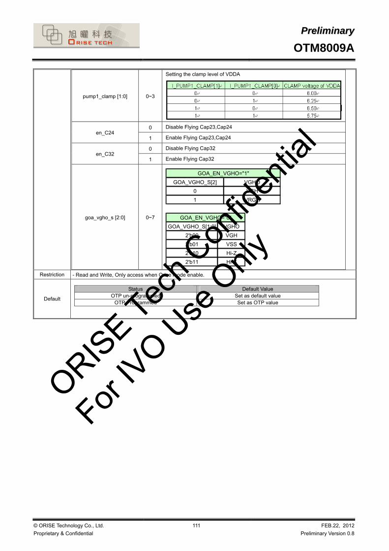
PPrreelliimmiinnaarryy
OTM8009A
© ORISE Technology Co., Ltd.
Proprietary & Confidential
111 FEB.22, 2012
Preliminary Version 0.8
pump1_clamp [1:0] 0~3
Setting the clamp level of VDDA
0 Disable Flying Cap23,Cap24 en_C24
1 Enable Flying Cap23,Cap24
0 Disable Flying Cap32 en_C32
1 Enable Flying Cap32
goa_vgho_s [2:0] 0~7
GOA_VGHO_S[2] VGHO
0 VGH
1 VRGH
GOA_EN_VGHO="1"
GOA_VGHO_S[1:0] VGHO
2'b00 VGH
2'b01 VSS
2'b10 Hi-Z
2'b11 Hi-Z
GOA_EN_VGHO="0"
Restriction - Read and Write, Only access when Orise mode enable.
Default
Status Default Value
OTP un-programmed Set as default value OTP Programmed Set as OTP value
ORISE Tec
h Con
fiden
tial
For IV
O Use
Only
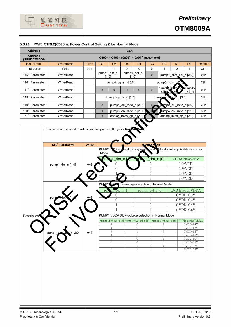
PPrreelliimmiinnaarryy
OTM8009A
© ORISE Technology Co., Ltd.
Proprietary & Confidential
112 FEB.22, 2012
Preliminary Version 0.8
5.3.21. PWR_CTRL2(C590h): Power Control Setting 2 for Normal Mode
Address C5h
Address (SPI/I2C/MDDI)
C590h~ C596h (0x91st ~ 0x97th parameter)
Inst. / Para. Write/Read D[15:8] D7 D6 D5 D4 D3 D2 D1 D0 Default
Instruction Write 00h 1 1 0 0 0 1 0 1 C5h
145th Parameter Write/Read
pump1_dm_n [1:0]
pump1_det_n [1:0]
0 pump1_dlvd_sel_n [2:0] 96h
146th Parameter Write/Read
pump4_vghs_n [3:0] pump5_vgls_n [3:0] 79h
147th Parameter Write/Read 0 0 0 0 0 pump4_
x6_n pump5_
x4_n pump45_x6_n
00h
148th Parameter Write/Read
hvreg_vrgh_s_n [3:0] hvreg_vglreg_s_n [3:0] 33h
149th Parameter Write/Read
0 pump1_clk_ratio_n [2:0] 0 pump2_clk_ratio_n [2:0] 33h
150th Parameter Write/Read 0 pump3_clk_ratio_n [2:0] 0 pump4_clk_ratio_n [2:0] 33h
151th Parameter Write/Read 0 analog_ibias_gp_n [2:0] 0 analog_ibias_ap_n [2:0] 43h
Description
- This command is used to adjust various pump settings for Normal Mode.
145th Parameter Value Description
pump1_dm_n [1:0] 0~3
PUMP1 DM in normal display region and DM auto setting disable in Normal Mode
pump1_dm_n [1] pump1_dm_n [0] VDDA pump-ratio
0 0 1.0*VDD
0 1 1.5*VDD
1 0 2.0*VDD
1 1 3.0*VDD
pump1_det_n [1:0] 0~3
PUMP1 VDDA low-voltage detection in Normal Mode
pump1_det_n [1] pump1_det_n [0] LVD level of VDDA
0 0 GVDD+0.3V
0 1 GVDD+0.4V
1 0 GVDD+0.5V
1 1 GVDD+0.6V
pump1_dlvd_sel_n [2:0] 0~7
PUMP1 VDDA Dlow-voltage detection in Normal Mode
pump1_dlvd_sel_n [2] pump1_dlvd_sel_n [1] pump1_dlvd_sel_n [0] DLVD level of VDDA
0 0 0 GVDD+1.4V
0 0 1 GVDD+1.3V
0 1 0 GVDD+1.2V
0 1 1 GVDD+1.1V
1 0 0 GVDD+1.0V
1 0 1 GVDD+0.9V
1 1 0 GVDD+0.8V
1 1 1 GVDD+0.7V
ORISE Tec
h Con
fiden
tial
For IV
O Use
Only

PPrreelliimmiinnaarryy
OTM8009A
© ORISE Technology Co., Ltd.
Proprietary & Confidential
113 FEB.22, 2012
Preliminary Version 0.8
146th Parameter Value Description
pump4_vghs_n [3:0] 0~15
PUMP4 VGH voltage select in Normal Mode pump4_vghs_n[3:0] VGH Voltage pump4_vghs_n[3:0] VGH Voltage
4’b0000 11.5 V 4’b1000 15.5 V
4’b0001 12.0 V 4’b1001 16.0 V
4’b0010 12.5 V 4’b1010 16.5 V
4’b0011 13.0 V 4’b1011 17.0 V
4’b0100 13.5 V 4’b1100 17.5 V
4’b0101 14.0 V 4’b1101 18.0 V
4’b0110 14.5 V 4’b1110 18.5 V
4’b0111 15.0 V 4’b1111 19.0 V
pump5_vgls_n [3:0] 0~15
PUMP5 VGL voltage select in Normal Mode
pump5_vgls_n[3:0] VGL Voltage pump5_vgls_n[3:0] VGL Voltage
4’b0000 -7.0 V 4’b1000 -11.5 V
4’b0001 -7.5 V 4’b1001 -12.0 V
4’b0010 -8.0 V 4’b1010 -12.5 V
4’b0011 -8.5 V 4’b1011 -13.0 V
4’b0100 -9.0 V 4’b1100 -14.0 V
4’b0101 -9.5 V 4’b1101 -14.5 V
4’b0110 -10.0 V 4’b1110 -15.0 V
4’b0111 -11.0 V 4’b1111 -15.5 V
147th Parameter Value Description
0 VGH = 8 X VDD, Only Valid when PUMP4_EN_ASDM_HV = ”0” pump4_x6_n
1 VGH = 6 X VDD, Only Valid when PUMP4_EN_ASDM_HV = ”0”
0 VGL = -6 X VDD, Only Valid when PUMP4_EN_ASDM_HV = ”0” pump5_x4_n
1 VGL = -4 X VDD, Only Valid when PUMP4_EN_ASDM_HV = ”0”
0 Set VGH by pump4_x6_n & set VGL by pump5_x4_n, Only Valid when PUMP4_EN_ASDM_HV = ”0”
pump45_x6_n
1 Set VGH = 6 X VDD & VGL = -6 X VDD , Only Valid when PUMP4_EN_ASDM_HV = ”0”
148th Parameter Value Description
hvreg_vrgh_s_n [3:0] 0~7
HV-regulator VRGH voltage select in Normal Mode
HVREG_VRGH_S[3:0] VRGH Voltage HVREG_VRGH_S[3:0] VRGH Voltage
4’b0000 8.5 V 4’b1000 12.5 V
4’b0001 9 V 4’b1001 13 V
4’b0010 9.5 V 4’b1010 13.5 V
4’b0011 10 V 4’b1011 14 V
4’b0100 10.5 V 4’b1100 14.5 V
4’b0101 11 V 4’b1101 15 V
4’b0110 11.5 V 4’b1110 15.5 V
4’b0111 12 V 4’b1111 16 V
hvreg_vglreg_s_n [3:0] 0~7
HV-regulator VGL-REG voltage select in Normal Mode
HVREG_VGLREG_S[3:0] VGL_REG Voltage HVREG_VGLREG_S[3:0] VGL_REG Voltage
4’b0000 -7.0 V 4’b1000 -11.5 V
4’b0001 -7.5 V 4’b1001 -12.0 V
4’b0010 -8.0 V 4’b1010 -12.5 V
4’b0011 -8.5 V 4’b1011 -13.0 V
4’b0100 -9.0 V 4’b1100 -14.0 V
4’b0101 -9.5 V 4’b1101 -14.5 V
4’b0110 -10.0 V 4’b1110 -15.0 V
4’b0111 -11.0 V 4’b1111 -15.5 V
ORISE Tec
h Con
fiden
tial
For IV
O Use
Only

PPrreelliimmiinnaarryy
OTM8009A
© ORISE Technology Co., Ltd.
Proprietary & Confidential
114 FEB.22, 2012
Preliminary Version 0.8
149th Parameter Value Description
pump1_clk_ratio_n [2:0] 0~7
PUMP1 set pump clock ratio
pump1_clk_ratio_n [2:0] VDDA Pump Clock Frequency
3’b000 8 Lines
3’b001 4 Lines
3’b010 2 Lines
3’b011 1 Line
3’b100 1 / 2 Line
3’b101 1 / 4 Line
3’b110 1 / 8 Line
3’b111 1 / 16 Line
pump2_clk_ratio_n [2:0] 0~7
PUMP2 set pump clock ratio
pump2_clk_ratio_n [2:0] NVDDA Pump Clock Frequency
3’b000 8 Lines
3’b001 4 Lines
3’b010 2 Lines
3’b011 1 Line
3’b100 1 / 2 Line
3’b101 1 / 4 Line
3’b110 1 / 8 Line
3’b111 1 / 16 Line
150th Parameter Value Description
pump3_clk_ratio_n [2:0] 0~7
PUMP3 set pump clock ratio
pump3_clk_ratio_n [2:0] VCL Pump Clock Frequency
3’b000 8 Lines
3’b001 4 Lines
3’b010 2 Lines
3’b011 1 Line
3’b100 1 / 2 Line
3’b101 1 / 4 Line
3’b110 1 / 8 Line
3’b111 1 / 16 Line
pump4_clk_ratio_n [2:0] 0~7
PUMP4 set pump clock ratio
pump4_clk_ratio_n [2:0] VGH/VGL Pump Clock Frequency
3’b000 8 Lines
3’b001 4 Lines
3’b010 2 Lines
3’b011 1 Line
3’b100 1 / 2 Line
3’b101 1 / 4 Line
3’b110 1 / 8 Line
3’b111 1 / 16 Line
151th Parameter Value Bias Current Selection
000 2.0 uA
001 2.5 uA
010 3.0 uA
011 3.5 uA
100 4.0 uA
101 4.5 uA
110 5.0 uA
analog_ibias_gp_n [2:0]
111 5.5 uA
ORISE Tec
h Con
fiden
tial
For IV
O Use
Only

PPrreelliimmiinnaarryy
OTM8009A
© ORISE Technology Co., Ltd.
Proprietary & Confidential
115 FEB.22, 2012
Preliminary Version 0.8
151th Parameter Value Trim Bias Current
000 60%
001 60%
010 70%
011 85%
100 100%
101 120%
110 140%
analog_ibias_ap_n [2:0]
111 160%
Restriction - Read and Write, Only access when Orise mode enable.
Default
Status Default Value
OTP un-programmed Set as default value OTP Programmed Set as OTP value
ORISE Tec
h Con
fiden
tial
For IV
O Use
Only

PPrreelliimmiinnaarryy
OTM8009A
© ORISE Technology Co., Ltd.
Proprietary & Confidential
116 FEB.22, 2012
Preliminary Version 0.8
5.3.22. PWR_CTRL3(C5A0h): Power Control Setting 3 for Idle Mode
Address C5h
Address (SPI/I2C/MDDI)
C5A0h~ C5A6h (0xA1st ~ 0xA7th parameter)
Inst. / Para. Write/Read D[15:8] D7 D6 D5 D4 D3 D2 D1 D0 Default
Instruction Write 00h 1 1 0 0 0 1 0 1 C5h
161th Parameter Write/Read
pump1_dm_i [1:0]
pump1_det_i [1:0]
0 pump1_dlvd_sel_i [2:0] 96h
162th Parameter Write/Read
pump4_vghs_i [3:0] pump5_vgls_i [3:0] 79h
163th Parameter Write/Read 0 0 0 0 0 pump4_
x6_i pump5_
x4_i pump45
_x6_i00h
164th Parameter Write/Read
hvreg_vrgh_s_i [3:0] hvreg_vglreg_s_i [3:0] 33h
165th Parameter Write/Read
0 pump1_clk_ratio_i [2:0] 0 pump2_clk_ratio_i [2:0] 33h
166th Parameter Write/Read
0 pump3_clk_ratio_i [2:0] 0 pump4_clk_ratio_i [2:0] 33h
167th Parameter Write/Read 0 analog_ibias_gp_i [2:0] 0 analog_ibias_ap_i [2:0] 43h
Description
- This command is used to adjust various pump settings for Idle Mode.
161th Parameter Value Description
pump1_dm_i [1:0] 0~3
PUMP1 DM in normal display region and DM auto setting disable in Normal Mode
pump1_dm_n [1] pump1_dm_n [0] VDDA pump-ratio
0 0 1.0*VDD
0 1 1.5*VDD
1 0 2.0*VDD
1 1 3.0*VDD
pump1_det_i [1:0] 0~3
PUMP1 VDDA low-voltage detection in Normal Mode
pump1_det_n [1] pump1_det_n [0] LVD level of VDDA
0 0 GVDD+0.3V
0 1 GVDD+0.4V
1 0 GVDD+0.5V
1 1 GVDD+0.6V
pump1_dlvd_sel_i [2:0] 0~7
PUMP1 VDDA Dlow-voltage detection in Normal Mode
pump1_dlvd_sel_n [2] pump1_dlvd_sel_n [1] pump1_dlvd_sel_n [0] DLVD level of VDDA
0 0 0 GVDD+1.4V
0 0 1 GVDD+1.3V
0 1 0 GVDD+1.2V
0 1 1 GVDD+1.1V
1 0 0 GVDD+1.0V
1 0 1 GVDD+0.9V
1 1 0 GVDD+0.8V
1 1 1 GVDD+0.7V
ORISE Tec
h Con
fiden
tial
For IV
O Use
Only

PPrreelliimmiinnaarryy
OTM8009A
© ORISE Technology Co., Ltd.
Proprietary & Confidential
117 FEB.22, 2012
Preliminary Version 0.8
162th Parameter Value Description
pump4_vghs_i [3:0] 0~15
PUMP4 VGH voltage select in Idle Mode
pump4_vghs_i[3:0] VGH Voltage pump4_vghs_i[3:0] VGH Voltage
4’b0000 11.5 V 4’b1000 15.5 V
4’b0001 12.0 V 4’b1001 16.0 V
4’b0010 12.5 V 4’b1010 16.5 V
4’b0011 13.0 V 4’b1011 17.0 V
4’b0100 13.5 V 4’b1100 17.5 V
4’b0101 14.0 V 4’b1101 18.0 V
4’b0110 14.5 V 4’b1110 18.5 V
4’b0111 15.0 V 4’b1111 19.0 V
pump5_vgls_i [3:0] 0~15
PUMP5 VGL voltage select in Idle Mode
pump5_vgls_i[3:0] VGL Voltage pump5_vgls_i[3:0] VGL Voltage
4’b0000 -7.0 V 4’b1000 -11.5 V
4’b0001 -7.5 V 4’b1001 -12.0 V
4’b0010 -8.0 V 4’b1010 -12.5 V
4’b0011 -8.5 V 4’b1011 -13.0 V
4’b0100 -9.0 V 4’b1100 -14.0 V
4’b0101 -9.5 V 4’b1101 -14.5 V
4’b0110 -10.0 V 4’b1110 -15.0 V
4’b0111 -11.0 V 4’b1111 -15.5 V
163th Parameter Value Description
0 VGH = 8 X VDD, Only Valid when PUMP4_EN_ASDM_HV = ”0” & “Idle Mode On”
pump4_x6_i
1 VGH = 6 X VDD, Only Valid when PUMP4_EN_ASDM_HV = ”0” & “Idle Mode On”
0 VGL = -6 X VDD, Only Valid when PUMP4_EN_ASDM_HV = ”0” & “Idle Mode On”
pump5_x4_i
1 VGL = -4 X VDD, Only Valid when PUMP4_EN_ASDM_HV = ”0” & “Idle Mode On”
0 Set VGH by pump4_x6_n & set VGL by pump5_x4_n, Only Valid when PUMP4_EN_ASDM_HV = ”0” & “Idle Mode On”
pump45_x6_i
1 Set VGH = 6 X VDD & VGL = -6 X VDD , Only Valid when PUMP4_EN_ASDM_HV = ”0” & “Idle Mode On”
164th Parameter Value Description
hvreg_vrgh_s_i [3:0] 0~7
HV-regulator VRGH voltage select in Idle Mode
HVREG_VRGH_S[3:0] VRGH Voltage HVREG_VRGH_S[3:0] VRGH Voltage
4’b0000 8.5 V 4’b1000 12.5 V
4’b0001 9 V 4’b1001 13 V
4’b0010 9.5 V 4’b1010 13.5 V
4’b0011 10 V 4’b1011 14 V
4’b0100 10.5 V 4’b1100 14.5 V
4’b0101 11 V 4’b1101 15 V
4’b0110 11.5 V 4’b1110 15.5 V
4’b0111 12 V 4’b1111 16 V
hvreg_vglreg_s_i [3:0] 0~7
HV-regulator VGL-REG voltage select in Idle Mode
HVREG_VGLREG_S[3:0] VGL_REG Voltage HVREG_VGLREG_S[3:0] VGL_REG Voltage
4’b0000 -7.0 V 4’b1000 -11.5 V
4’b0001 -7.5 V 4’b1001 -12.0 V
4’b0010 -8.0 V 4’b1010 -12.5 V
4’b0011 -8.5 V 4’b1011 -13.0 V
4’b0100 -9.0 V 4’b1100 -14.0 V
4’b0101 -9.5 V 4’b1101 -14.5 V
4’b0110 -10.0 V 4’b1110 -15.0 V
4’b0111 -11.0 V 4’b1111 -15.5 V
ORISE Tec
h Con
fiden
tial
For IV
O Use
Only

PPrreelliimmiinnaarryy
OTM8009A
© ORISE Technology Co., Ltd.
Proprietary & Confidential
118 FEB.22, 2012
Preliminary Version 0.8
165th Parameter Value Description
pump1_clk_ratio_i [2:0] 0~7
PUMP1 set pump clock ratio
pump1_clk_ratio_i [2:0] VDDA Pump Clock Frequency
3’b000 8 Lines
3’b001 4 Lines
3’b010 2 Lines
3’b011 1 Line
3’b100 1 / 2 Line
3’b101 1 / 4 Line
3’b110 1 / 8 Line
3’b111 1 / 16 Line
pump2_clk_ratio_i [2:0] 0~7
PUMP2 set pump clock ratio
pump2_clk_ratio_i [2:0] NVDDA Pump Clock Frequency
3’b000 8 Lines
3’b001 4 Lines
3’b010 2 Lines
3’b011 1 Line
3’b100 1 / 2 Line
3’b101 1 / 4 Line
3’b110 1 / 8 Line
3’b111 1 / 16 Line
166th Parameter Value Description
pump3_clk_ratio_i [2:0] 0~7
PUMP3 set pump clock ratio
pump3_clk_ratio_i [2:0] VCL Pump Clock Frequency
3’b000 8 Lines
3’b001 4 Lines
3’b010 2 Lines
3’b011 1 Line
3’b100 1 / 2 Line
3’b101 1 / 4 Line
3’b110 1 / 8 Line
3’b111 1 / 16 Line
pump4_clk_ratio_i [2:0] 0~7
PUMP4 set pump clock ratio
pump4_clk_ratio_i [2:0] VGH/VGL Pump Clock Frequency
3’b000 8 Lines
3’b001 4 Lines
3’b010 2 Lines
3’b011 1 Line
3’b100 1 / 2 Line
3’b101 1 / 4 Line
3’b110 1 / 8 Line
3’b111 1 / 16 Line
ORISE Tec
h Con
fiden
tial
For IV
O Use
Only

PPrreelliimmiinnaarryy
OTM8009A
© ORISE Technology Co., Ltd.
Proprietary & Confidential
119 FEB.22, 2012
Preliminary Version 0.8
167th Parameter Value Bias Current Selection
000 2.0 uA
001 2.5 uA
010 3.0 uA
011 3.5 uA
100 4.0 uA
101 4.5 uA
110 5.0 uA
analog_ibias_gp_i [2:0]
111 5.5 uA
167th Parameter Value Trim Bias Current
000 60%
001 60%
010 70%
011 85%
100 100%
101 120%
110 140%
analog_ibias_ap_i [2:0]
111 160%
Restriction - Read and Write, Only access when Orise mode enable.
Default
Status Default Value
OTP un-programmed Set as default value OTP Programmed Set as OTP value
ORISE Tec
h Con
fiden
tial
For IV
O Use
Only

PPrreelliimmiinnaarryy
OTM8009A
© ORISE Technology Co., Ltd.
Proprietary & Confidential
120 FEB.22, 2012
Preliminary Version 0.8
5.3.23. PWR_CTRL4(C5B0h): Power Control Setting 4 for DC Voltage Settings
Address C5h
Address (SPI/I2C/MDDI)
C5B0h ~ C5B1h (0xB1st ~ 0xB2th parameter)
Inst. / Para. Write/Read D[15:8] D7 D6 D5 D4 D3 D2 D1 D0 Default
Instruction Write 00h 1 1 0 0 0 1 0 1 C5h
177th Parameter Write/Read pwr_te_
sel pwr_led
_selsmpwid [4:0] 04h
178th Parameter Write/Read vdd18v_sel [1:0] lvdsvdd_sel [1:0]diopwr_
sel 0
gvdd_vcom_gn
d
gvdd_en_test
A8h
Description
- pwr_te_sel : select TE output voltage level
- pwr_led_sel : select LEDON/LEDPWM output voltage level
pwr_te_sel = 0 pwr_te_sel = 1 pwr_led_sel=0 pwr_led_sel=1
Low 1.2vVOH=VDDIO
VOL=VSSVOH=VDDVOL=VSS
High 1.8vVOH=VDDIO
VOL=VSSVOH=VDDVOL=VSS
Low 1.2v
High 1.8vVOH=VDDIO
VOL=VSSVOH=DIOPW
RVOH=VDDIO
VOL=VSSVOH=VDDVOL=VSS
Low 1.2v
High 1.8v1.1~1.3v1
VOH=DIOPWRVOL=VSS
VOH=DIOPWRVOL=VSS
VOH=DIOPWRVOL=VSS
VOH=DIOPWRVOL=VSS
VOH=VDDIOVOL=VSS
Output voltage levelTE LEDON, LEDPWM
VOH=VDDIOVOL=VSS
1 1.65~3.3v
VOH=DIOPWRVOL=VSS
VOH=DIOPWRVOL=VSS
DSTB_SEL VDDIO
01.65~3.3v
or1.1~1.3v
VSEL DIOPWR
177th Parameter Value Description
smpwid [4:0] 0~15
VCOM sample hold pulse width x
178th Parameter Value Voltage Selection for VDD_18V
00 1.70V
01 1.65V
10 1.60V vdd18v_sel [1:0]
11 1.55V
178th Parameter Value Voltage Selection for LVDSVDD
00 1.70V
01 1.65V
10 1.60V lvdsvdd_sel [1:0]
11 1.55V
ORISE Tec
h Con
fiden
tial
For IV
O Use
Only

PPrreelliimmiinnaarryy
OTM8009A
© ORISE Technology Co., Ltd.
Proprietary & Confidential
121 FEB.22, 2012
Preliminary Version 0.8
178th Parameter Value Description
0 1.2V diopwr_sel
1 1.8V
0 VCOMDC voltage be set by vcom_vmdc[7:0] gvdd_vcom_gnd
1 VCOMDC voltage set to GND
0 Disable VCOM test mode gvdd_en_test
1 Enable VCOM test mode
Restriction - Read and Write, Only access when Orise mode enable.
Default
Status Default Value
OTP un-programmed Set as default value OTP Programmed Set as OTP value
ORISE Tec
h Con
fiden
tial
For IV
O Use
Only

PPrreelliimmiinnaarryy
OTM8009A
© ORISE Technology Co., Ltd.
Proprietary & Confidential
122 FEB.22, 2012
Preliminary Version 0.8
5.3.24. PWM_PARA1 (C680H) PWM Parameter 1
Address C6h
Address (SPI/I2C/MDDI)
C680h (0x81st parameter)
Inst. / Para. Write/Read D[15:8] D7 D6 D5 D4 D3 D2 D1 D0 Default
Instruction Write 00h 1 1 0 0 0 1 1 0 C6h
129’th Parameter Write/Read 1 BCENECABC_
EN 1 0
BC_SEL
0 0 F4h
Description
- This command is used to set the internal function block of LPWM.
-BCENE : This bit combine with BC_SEL register to control LEDPWM PIN output.
- CABC_EN : This bit is used to control CABC related Command enable (include: $51,$53, $55, $5E)
CABC_EN5[D5] CABC related Command0 Disable
1 Enable(Default)
- BC_SEL : This bit combine with BCENE and BC_OEN_OPT register to control LEDPWM PIN output.
Restriction - Read and Write, Only access when Orise mode enable.
Default
Status Default Value
OTP un-programmed Set as default value OTP Programmed Set as OTP value
BC_SEL Control LEDPWM
0 Disable, LEDPWM=0
1 Enable, if BC_SEL=1, LEDPWM output BC pulse
BCENE
BC_SEL
LEDPWM PAD
Enable
LEDPWMBC
BC_OEN_OPT
ORISE Tec
h Con
fiden
tial
For IV
O Use
Only

PPrreelliimmiinnaarryy
OTM8009A
© ORISE Technology Co., Ltd.
Proprietary & Confidential
123 FEB.22, 2012
Preliminary Version 0.8
5.3.25. PWM_PARA2 (C6B0H) PWM Parameter 2
Address C6h
Address (SPI/I2C/MDDI)
C6B0h (0xB1st parameter)
Inst. / Para. Write/Read D[15:8] D7 D6 D5 D4 D3 D2 D1 D0 Default
Instruction Write 00h 1 1 0 0 0 1 1 0 C6h
177th Parameter Write/Read PWM_POL
0 0 0 BC_MO
D[1]BC_MO
D[0] 1 1 03h
Description
- BC_MOD[1:0] : 00 : BC pulse will not be clear by Vsync signal. 01 : BC pulse will be clear by Vsync pulse sigmal.
- PWM_POL : Polarity of LEDPWM output.
Restriction - Read and Write, Only access when Orise mode enable.
Default
Status Default Value
OTP un-programmed Set as default value OTP Programmed Set as OTP value
ORISE Tec
h Con
fiden
tial
For IV
O Use
Only

PPrreelliimmiinnaarryy
OTM8009A
© ORISE Technology Co., Ltd.
Proprietary & Confidential
124 FEB.22, 2012
Preliminary Version 0.8
5.3.26. PWM_PARA3 (C6B1H) PWM Parameter 3
Address C6h
Address (SPI/I2C/MDDI)
C6B1h (0xB2nd parameter)
Inst. / Para. Write/Read D[15:8] D7 D6 D5 D4 D3 D2 D1 D0 Default
Instruction Write 00h 1 1 0 0 0 1 1 0 C6h
178th Parameter Write/Read DBF[7] DBF[6] DBF[5] DBF[4] DBF[3] DBF[2] DBF[1] DBF[0] 10h
Description
- This command is used to adjust PWM Freq. The PWM Freq can be set by DBF and PWM_FREQ_SEL as following table.
DBF[7:0] DBF[7:0] DBF[7:0]
00 01 10 11 00 01 10 11 00 01 10 11
0 66.406 132.812 33.203 16.601 44 1.475 2.951 0.737 0.368 88 0.746 1.492 0.373 0.186
1 33.203 66.406 16.601 8.3 45 1.443 2.887 0.721 0.36 89 0.737 1.475 0.368 0.184
2 22.135 44.27 11.067 5.533 46 1.412 2.825 0.706 0.353 90 0.729 1.459 0.364 0.182
3 16.601 33.203 8.3 4.15 47 1.383 2.766 0.691 0.345 91 0.721 1.443 0.36 0.18
4 13.281 26.562 6.64 3.32 48 1.355 2.71 0.677 0.338 92 0.714 1.428 0.357 0.178
5 11.067 22.135 5.533 2.766 49 1.328 2.656 0.664 0.332 93 0.706 1.412 0.353 0.176
6 9.486 18.973 4.743 2.371 50 1.302 2.604 0.651 0.325 94 0.699 1.398 0.349 0.174
7 8.3 16.601 4.15 2.075 51 1.277 2.554 0.638 0.319 95 0.691 1.383 0.345 0.172
8 7.378 14.756 3.689 1.844 52 1.252 2.505 0.626 0.313 96 0.684 1.369 0.342 0.171
9 6.64 13.281 3.32 1.66 53 1.229 2.459 0.614 0.307 97 0.677 1.355 0.338 0.169
10 6.036 12.073 3.018 1.509 54 1.207 2.414 0.603 0.301 98 0.67 1.341 0.335 0.167
11 5.533 11.067 2.766 1.383 55 1.185 2.371 0.592 0.296 99 0.664 1.328 0.332 0.166
12 5.108 10.216 2.554 1.277 56 1.165 2.33 0.582 0.291 100 0.657 1.314 0.328 0.164
13 4.743 9.486 2.371 1.185 57 1.144 2.289 0.572 0.286 101 0.651 1.302 0.325 0.162
14 4.427 8.854 2.213 1.106 58 1.125 2.251 0.562 0.281 102 0.644 1.289 0.322 0.161
15 4.15 8.3 2.075 1.037 59 1.106 2.213 0.553 0.276 103 0.638 1.277 0.319 0.159
16 3.906 7.812 1.953 0.976 60 1.088 2.177 0.544 0.272 104 0.632 1.264 0.316 0.158
17 3.689 7.378 1.844 0.922 61 1.071 2.142 0.535 0.267 105 0.626 1.252 0.313 0.156
18 3.495 6.99 1.747 0.873 62 1.054 2.108 0.527 0.263 106 0.62 1.241 0.31 0.155
19 3.32 6.64 1.66 0.83 63 1.037 2.075 0.518 0.259 107 0.614 1.229 0.307 0.153
20 3.162 6.324 1.581 0.79 64 1.021 2.043 0.51 0.255 108 0.609 1.218 0.304 0.152
21 3.018 6.036 1.509 0.754 65 1.006 2.012 0.503 0.251 109 0.603 1.207 0.301 0.15
22 2.887 5.774 1.443 0.721 66 0.991 1.982 0.495 0.247 110 0.598 1.196 0.299 0.149
23 2.766 5.533 1.383 0.691 67 0.976 1.953 0.488 0.244 111 0.592 1.185 0.296 0.148
24 2.656 5.312 1.328 0.664 68 0.962 1.924 0.481 0.24 112 0.587 1.175 0.293 0.146
25 2.554 5.108 1.277 0.638 69 0.948 1.897 0.474 0.237 113 0.582 1.165 0.291 0.145
26 2.459 4.918 1.229 0.614 70 0.935 1.87 0.467 0.233 114 0.577 1.154 0.288 0.144
27 2.371 4.743 1.185 0.592 71 0.922 1.844 0.461 0.23 115 0.572 1.144 0.286 0.143
28 2.289 4.579 1.144 0.572 72 0.909 1.819 0.454 0.227 116 0.567 1.135 0.283 0.141
29 2.213 4.427 1.106 0.553 73 0.897 1.794 0.448 0.224 117 0.562 1.125 0.281 0.14
30 2.142 4.284 1.071 0.535 74 0.885 1.77 0.442 0.221 118 0.558 1.116 0.279 0.139
31 2.075 4.15 1.037 0.518 75 0.873 1.747 0.436 0.218 119 0.553 1.106 0.276 0.138
32 2.012 4.024 1.006 0.503 76 0.862 1.724 0.431 0.215 120 0.548 1.097 0.274 0.137
33 1.953 3.906 0.976 0.488 77 0.851 1.702 0.425 0.212 121 0.544 1.088 0.272 0.136
34 1.897 3.794 0.948 0.474 78 0.84 1.681 0.42 0.21 122 0.539 1.079 0.269 0.134
35 1.844 3.689 0.922 0.461 79 0.83 1.66 0.415 0.207 123 0.535 1.071 0.267 0.133
36 1.794 3.589 0.897 0.448 80 0.819 1.639 0.409 0.204 124 0.531 1.062 0.265 0.132
37 1.747 3.495 0.873 0.436 81 0.809 1.619 0.404 0.202 125 0.527 1.054 0.263 0.131
38 1.702 3.405 0.851 0.425 82 0.8 1.6 0.4 0.2 126 0.522 1.045 0.261 0.13
39 1.66 3.32 0.83 0.415 83 0.79 1.581 0.395 0.197 127 0.518 1.037 0.259 0.129
40 1.619 3.239 0.809 0.404 84 0.781 1.562 0.39 0.195 128 0.514 1.029 0.257 0.128
41 1.581 3.162 0.79 0.395 85 0.772 1.544 0.386 0.193 129 0.51 1.021 0.255 0.127
42 1.544 3.088 0.772 0.386 86 0.763 1.526 0.381 0.19 130 0.506 1.013 0.253 0.126
43 1.509 3.018 0.754 0.377 87 0.754 1.509 0.377 0.188 131 0.503 1.006 0.251 0.125
PWM_FREQ_SEL[1:0](KHz) PWM_FREQ_SEL[1:0](KHz) PWM_FREQ_SEL[1:0](KHz)
ORISE Tec
h Con
fiden
tial
For IV
O Use
Only

PPrreelliimmiinnaarryy
OTM8009A
© ORISE Technology Co., Ltd.
Proprietary & Confidential
125 FEB.22, 2012
Preliminary Version 0.8
DBF[7:0] DBF[7:0] DBF[7:0]
00 01 10 11 00 01 10 11 00 01 10 11
132 0.499 0.998 0.249 0.124 176 0.375 0.75 0.187 0.093 220 0.3 0.6 0.15 0.075
133 0.495 0.991 0.247 0.123 177 0.373 0.746 0.186 0.093 221 0.299 0.598 0.149 0.074
134 0.491 0.983 0.245 0.122 178 0.37 0.741 0.185 0.092 222 0.297 0.595 0.148 0.074
135 0.488 0.976 0.244 0.122 179 0.368 0.737 0.184 0.092 223 0.296 0.592 0.148 0.074
136 0.484 0.969 0.242 0.121 180 0.366 0.733 0.183 0.091 224 0.295 0.59 0.147 0.073
137 0.481 0.962 0.24 0.12 181 0.364 0.729 0.182 0.091 225 0.293 0.587 0.146 0.073
138 0.477 0.955 0.238 0.119 182 0.362 0.725 0.181 0.09 226 0.292 0.585 0.146 0.073
139 0.474 0.948 0.237 0.118 183 0.36 0.721 0.18 0.09 227 0.291 0.582 0.145 0.072
140 0.47 0.941 0.235 0.117 184 0.358 0.717 0.179 0.089 228 0.289 0.579 0.144 0.072
141 0.467 0.935 0.233 0.116 185 0.357 0.714 0.178 0.089 229 0.288 0.577 0.144 0.072
142 0.464 0.928 0.232 0.116 186 0.355 0.71 0.177 0.088 230 0.287 0.574 0.143 0.071
143 0.461 0.922 0.23 0.115 187 0.353 0.706 0.176 0.088 231 0.286 0.572 0.143 0.071
144 0.457 0.915 0.228 0.114 188 0.351 0.702 0.175 0.087 232 0.285 0.57 0.142 0.071
145 0.454 0.909 0.227 0.113 189 0.349 0.699 0.174 0.087 233 0.283 0.567 0.141 0.07
146 0.451 0.903 0.225 0.112 190 0.347 0.695 0.173 0.086 234 0.282 0.565 0.141 0.07
147 0.448 0.897 0.224 0.112 191 0.345 0.691 0.172 0.086 235 0.281 0.562 0.14 0.07
148 0.445 0.891 0.222 0.111 192 0.344 0.688 0.172 0.086 236 0.28 0.56 0.14 0.07
149 0.442 0.885 0.221 0.11 193 0.342 0.684 0.171 0.085 237 0.279 0.558 0.139 0.069
150 0.439 0.879 0.219 0.109 194 0.34 0.681 0.17 0.085 238 0.277 0.555 0.138 0.069
151 0.436 0.873 0.218 0.109 195 0.338 0.677 0.169 0.084 239 0.276 0.553 0.138 0.069
152 0.434 0.868 0.217 0.108 196 0.337 0.674 0.168 0.084 240 0.275 0.551 0.137 0.068
153 0.431 0.862 0.215 0.107 197 0.335 0.67 0.167 0.083 241 0.274 0.548 0.137 0.068
154 0.428 0.856 0.214 0.107 198 0.333 0.667 0.166 0.083 242 0.273 0.546 0.136 0.068
155 0.425 0.851 0.212 0.106 199 0.332 0.664 0.166 0.083 243 0.272 0.544 0.136 0.068
156 0.422 0.845 0.211 0.105 200 0.33 0.66 0.165 0.082 244 0.271 0.542 0.135 0.067
157 0.42 0.84 0.21 0.105 201 0.328 0.657 0.164 0.082 245 0.269 0.539 0.134 0.067
158 0.417 0.835 0.208 0.104 202 0.327 0.654 0.163 0.081 246 0.268 0.537 0.134 0.067
159 0.415 0.83 0.207 0.103 203 0.325 0.651 0.162 0.081 247 0.267 0.535 0.133 0.066
160 0.412 0.824 0.206 0.103 204 0.323 0.647 0.161 0.08 248 0.266 0.533 0.133 0.066
161 0.409 0.819 0.204 0.102 205 0.322 0.644 0.161 0.08 249 0.265 0.531 0.132 0.066
162 0.407 0.814 0.203 0.101 206 0.32 0.641 0.16 0.08 250 0.264 0.529 0.132 0.066
163 0.404 0.809 0.202 0.101 207 0.319 0.638 0.159 0.079 251 0.263 0.527 0.131 0.065
164 0.402 0.804 0.201 0.1 208 0.317 0.635 0.158 0.079 252 0.262 0.524 0.131 0.065
165 0.4 0.8 0.2 0.1 209 0.316 0.632 0.158 0.079 253 0.261 0.522 0.13 0.065
166 0.397 0.795 0.198 0.099 210 0.314 0.629 0.157 0.078 254 0.26 0.52 0.13 0.065
167 0.395 0.79 0.197 0.098 211 0.313 0.626 0.156 0.078 255 0.259 0.518 0.129 0.064
168 0.392 0.785 0.196 0.098 212 0.311 0.623 0.155 0.077
169 0.39 0.781 0.195 0.097 213 0.31 0.62 0.155 0.077
170 0.388 0.776 0.194 0.097 214 0.308 0.617 0.154 0.077
171 0.386 0.772 0.193 0.096 215 0.307 0.614 0.153 0.076
172 0.383 0.767 0.191 0.095 216 0.306 0.612 0.153 0.076
173 0.381 0.763 0.19 0.095 217 0.304 0.609 0.152 0.076
174 0.379 0.758 0.189 0.094 218 0.303 0.606 0.151 0.075
175 0.377 0.754 0.188 0.094 219 0.301 0.603 0.15 0.075
PWM_FREQ_SEL[1:0](KHz) PWM_FREQ_SEL[1:0](KHz)PWM_FREQ_SEL[1:0](KHz)
Restriction - Read and Write, Only access when Orise mode enable.
Default
Status Default Value
OTP un-programmed Set as default value OTP Programmed Set as OTP value
ORISE Tec
h Con
fiden
tial
For IV
O Use
Only

PPrreelliimmiinnaarryy
OTM8009A
© ORISE Technology Co., Ltd.
Proprietary & Confidential
126 FEB.22, 2012
Preliminary Version 0.8
5.3.27. PWM_PARA4 (C6B3H) PWM Parameter 4
Address C6h
Address (SPI/I2C/MDDI)
C6B3h (0xB4th parameter)
Inst. / Para. Write/Read D[15:8] D7 D6 D5 D4 D3 D2 D1 D0 Default
Instruction Write 00h 1 1 0 0 0 1 1 0 C6h
180th Parameter Write/Read DFBCLEDON
_ENLEDON_POL
LPWM_DIM_
FRM[4]
LPWM_DIM_
FRM[3]
LPWM_ DIM_
FRM[2]
LPWM_ DIM_
FRM[1]
LPWM_DIM_
FRM[0]5Fh
Description
- This command is used to set LEDPWM setting.
- DFBC :Default BC status before Power-ON.
DFBC[D7] Default BC status before Power-ON.
0 LEDPWM=’low’
1 LEDPWM=’High
Note. It also XOR with “LPWM Parameter 9” PWM_POL.
- LEDON_EN : Enable LEDON PAD for external LED Driver
LEDON_EN[D6] LEDON PAD for external LED Driver
0 Disable
1 Enable(Default)
Note. This function only active when $53_BL=1.
- LEDON_POL: Polarity of LEDON Control Signal
LEDON_POL[D5] Polarity of LEDON Control Signal
0 Noraml(Default).
1 Inversion.
Note. This function only active when $53_BL=1 and LEDON_EN=’1’.
- LPWM_DIM_FRM[4:0] : LPWM Dimming frame, Default is 32 Frame.
LPWM_DIM_FRM[4:0] Frame
00h 1
01h 2
… …
1Eh 31
1Fh 32
Restriction - Read and Write, Only access when Orise mode enable.
Default
Status Default Value
OTP un-programmed Set as default value OTP Programmed Set as OTP value
ORISE Tec
h Con
fiden
tial
For IV
O Use
Only

PPrreelliimmiinnaarryy
OTM8009A
© ORISE Technology Co., Ltd.
Proprietary & Confidential
127 FEB.22, 2012
Preliminary Version 0.8
5.3.28. PWM_PARA5 (C6B4H) PWM Parameter 5
Address C6h
Address (SPI/I2C/MDDI)
C6B4h (0xB5th parameter)
Inst. / Para. Write/Read D[15:8] D7 D6 D5 D4 D3 D2 D1 D0 Default
Instruction Write 00h 1 1 0 0 0 1 1 0 C6h
181th Parameter Write/Read 0 0 0 BC_OEN_OPT
0 PWM_ FREQ_ SEL[1]
PWM_ FREQ_ SEL[0]
CABC_DUTY_FORCE
12h
Description
- This command is used to set PWM Frequency setting.
- BC_OEN_OPT : If BC_OEN_OPT=1, the LCDPWM pad always output.
BC_SEL Control LEDPWM
0 Disable, LEDPWM=0
1 Enable, if BC_SEL=1, LEDPWM output BC pulse
BCENE
BC_SEL
LEDPWM PAD
Enable
LEDPWMBC
BC_OEN_OPT
- PWM_FREQ_SEL[1:0]: Please refer “LPWM Parameter 10”
- CABC_DUTY_FORCE: Selector for giving a specific value to CABC Block. Please refer “PWM Control Architecture”
Restriction - Read and Write, Only access when Orise mode enable.
Default
Status Default Value
OTP un-programmed Set as default value OTP Programmed Set as OTP value
ORISE Tec
h Con
fiden
tial
For IV
O Use
Only

PPrreelliimmiinnaarryy
OTM8009A
© ORISE Technology Co., Ltd.
Proprietary & Confidential
128 FEB.22, 2012
Preliminary Version 0.8
5.3.29. PWM_PARA6 (C6B5H) PWM Parameter 6
Address C6h
Address (SPI/I2C/MDDI)
C6B5h (0xB6th parameter)
Inst. / Para. Write/Read D[15:8] D7 D6 D5 D4 D3 D2 D1 D0 Default
Instruction Write 00h 1 1 0 0 0 1 1 0 C6h
182th Parameter Write/Read CABC_DUTY_SET[7]
CABC_DUTY_SET[6]
CABC_DUTY_SET[5]
CABC_DUTY_SET[4]
CABC_DUTY_SET[3]
CABC_ DUTY_ SET[2]
CABC_ DUTY_ SET[1]
CABC_DUTY_SET[0]
00h
Description - This command is used to set specific CABC value.
- CABC_DUTY_SET[7:0] : Giving Specific CABC Value for debug. Note: This function only active when “CABC_DUTY_FORCE” = ‘1’.
Restriction - Read and Write, Only access when Orise mode enable.
Default
Status Default Value
OTP un-programmed Set as default value OTP Programmed Set as OTP value
ORISE Tec
h Con
fiden
tial
For IV
O Use
Only

PPrreelliimmiinnaarryy
OTM8009A
© ORISE Technology Co., Ltd.
Proprietary & Confidential
129 FEB.22, 2012
Preliminary Version 0.8
5.3.30. CABCSET1 (C700h): CABC Setting
Address C7h
Address (SPI/I2C/MDDI)
C700h (0x01stparameter)
Inst. / Para. Write/Read D[15:8] D7 D6 D5 D4 D3 D2 D1 D0 Default
Instruction Write 00h 1 1 0 0 0 1 1 1 C7h
Parameter 1 Write 0 0 0 CABC_SEL_E
NA CABC_SEL[3:0] 0Fh
Description
- CABC_SEL_ENA: CABC Manual Setting Enable
- CABC_SEL[3:0]: CABC Manual Gamma Curve Select
Orise engineer mode enableCmd FFh parameter 80h,09h,01h
Cmd 00h parameter 80h
Cmd FFh parameter 80h,09h
Orise Address shift enableCmd 00h parameter 00h
CABC Gamma Curve selectCmd C7h parameter 1
CABC Gamma Curve SettingCmd C8h parameter (18 parameters)
Orise Address shift enableCmd 00h parameter 00h
Orise Address shift enableCmd 00h parameter 00h
CABC Gamma Curve selectCmd C7h parameter 00h
Restriction - Write, Only access when Orise mode enable.
Default
Status Default Value
OTP un-programmed No OTP Support OTP Programmed No OTP Support
ORISE Tec
h Con
fiden
tial
For IV
O Use
Only

PPrreelliimmiinnaarryy
OTM8009A
© ORISE Technology Co., Ltd.
Proprietary & Confidential
130 FEB.22, 2012
Preliminary Version 0.8
5.3.31. CABCSET2 (C800h): CABC gamma curve setting
Address C8h
Address (SPI/I2C/MDDI)
C800h~C811 (0x01st ~0x12th parameter)
Inst. / Para. Write/Read D[15:8] D7 D6 D5 D4 D3 D2 D1 D0 Default
Instruction Write 00h 1 1 0 0 1 0 0 0
Parameter 1 Write/Read CABC2[3:0] CABC1[3:0] 80h
Parameter 2 Write/Read CABC4[3:0] CABC3[3:0] 88h
Parameter 3 Write/Read CABC6[3:0] CABC5[3:0] 88h
Parameter 4 Write/Read CABC8[3:0] CABC7[3:0] 88h
Parameter 5 Write/Read CABC10[3:0] CABC9[3:0] 88h
Parameter 6 Write/Read CABC12[3:0] CABC11[3:0] 88h
Parameter 7 Write/Read CABC14[3:0] CABC13[3:0] 88h
Parameter 8 Write/Read CABC16[3:0] CABC15[3:0] 88h
Parameter 9 Write/Read CABC18[3:0] CABC17[3:0] 88h
Parameter 10 Write/Read CABC20[3:0] CABC19[3:0] 88h
Parameter 11 Write/Read CABC22[3:0] CABC21[3:0] 88h
Parameter 12 Write/Read CABC24[3:0] CABC23[3:0] 88h
Parameter 13 Write/Read CABC26[3:0] CABC25[3:0] 88h
Parameter 14 Write/Read CABC28[3:0] CABC27[3:0] 88h
Parameter 15 Write/Read CABC30[3:0] CABC29[3:0] 88h
Parameter 16 Write/Read CABC32[3:0] CABC31[3:0] 88h
Parameter 17 Write/Read CABC34[3:0] CABC33[3:0] 88h
Parameter 18 Write/Read CABC36[3:0] CABC35[3:0] 88h
Description - CABCx[3:0] (x=1~18): Command C8h totally has 18 parameters, these parameters are settings for CABC gamma curve
Restriction - Read and Write, Only access when Orise mode enable.
Default
Status Default Value
OTP un-programmed Set as default value OTP Programmed Set as OTP value
ORISE Tec
h Con
fiden
tial
For IV
O Use
Only

PPrreelliimmiinnaarryy
OTM8009A
© ORISE Technology Co., Ltd.
Proprietary & Confidential
131 FEB.22, 2012
Preliminary Version 0.8
5.3.32. AIESET(C900h): AIE Setting
Address (MIPI) C9h
Address (Other I/F)
C900h
Inst. / Para. Write/Read D[15:8] D7 D6 D5 D4 D3 D2 D1 D0 Default
Instruction Write 00h 1 1 0 0 1 0 0 1 C9h
1st Parameter Write/Read AIE2[3:0] AIE1[3:0] 80h
2nd Parameter Write/Read AIE4[3:0] AIE3[3:0] 88h
: Write/Read : : 88h
17th Parameter Write/Read AIE34[3:0] AIE33[3:0] 88h
18th Parameter Write/Read AIE36[3:0] AIE35[3:0] 88h
Description - Command C9h totally has 18 parameters, these parameters are settings for AIE gamma curve
Restriction - Read and Write, Only access when Orise mode enable.
Default
Status Default Value OTP un-programmed Set as default value
OTP Programmed Set as OTP value
ORISE Tec
h Con
fiden
tial
For IV
O Use
Only

PPrreelliimmiinnaarryy
OTM8009A
© ORISE Technology Co., Ltd.
Proprietary & Confidential
132 FEB.22, 2012
Preliminary Version 0.8
5.3.33. GOAVST(CE80h~CE8Bh) GOA VST Setting
Address CEh
Address (SPI/I2C/MDDI)
CE80h ~ CE8Bh (0x81st ~ 0x8Cth parameter)
Inst. / Para. Write/Read D[15:8] D7 D6 D5 D4 D3 D2 D1 D0 Default
Instruction Write 00h 1 1 0 0 1 1 1 0
0x81st Parameter Write/Read vst1_shift[7:0] 82h
0x82nd Parameter Write/Read 0 0 0 0 vst1_width[3:0] 01h
0x83rd Parameter Write/Read vst1_tchop[7:0] 28h
0x84th Parameter Write/Read vst2_shift[7:0] 81h
0x85th Parameter Write/Read 0 0 0 0 vst2_width[3:0] 01h
0x86th Parameter Write/Read vst2_tchop[7:0] 28h
0x87th Parameter Write/Read vst3_shift[7:0] 81h
0x88th Parameter Write/Read 0 0 0 0 vst3_width[3:0] 01h
0x89th Parameter Write/Read vst3_tchop[7:0] 28h
0x8Ath Parameter Write/Read vst4_shift[7:0] 82h
0x8Bth Parameter Write/Read 0 0 0 0 vst4_width[3:0] 01h
0x8Cth Parameter Write/Read vst4_tchop[7:0] 28h
Description
These parameters are used to create single pulse type signals tcon_goa_vst1, tcon_goa_vst2, tcon_goa_vst3 and tcon_goa_vst4.
Parameters Description
vst1_shift[7] 0: tcon_goa_vst1 rising edge locates after reference point
1: tcon_goa_vst1 rising edge locates before reference point, in BP region
vst1_shift[6:0] Set starting position of the tcon_goa_vst1 pulse with respect to the reference point
vst1_width[3:0] Set tcon_goa_vst1 pulse width = vst1_width[3:0] + 1 (unit = line)
vst1_tchop[7:0] Delay rising edge of tcon_goa_vst1 signal (unit = mclk)
BP BP BP BP BP BP BP BP 0 1 2 3 4 5 6 7 ... 956 957 958 959 FP FP FP FP FP FP FP
vst1_shift[6:0](if vst1_shift[7] == 1)
(If vst1_shift[7] == 0)
vst1_tchop[7:0]tcon_goa_vst1
tcon_goa_vst1
8 9 10 11 12 13 14BP BP BP
goa_vst1_shift[7:0] = 82h
goa_vst1_shift[7:0] = 07h
referencepoint
vst1_shift[6:0]
vst1_width[3:0]
vst1_width[3:0]
linecnt_shift1[15:0]
- Use other parameters and apply the same method to create tcon_goa_vst2, tcon_goa_vst3 and tcon_goa_vst4 signals
Restriction - Read and Write, Only accessible when Orise mode is enabled.
Default
Status Default Value
OTP un-programmed Set as default value OTP Programmed Set as OTP value
ORISE Tec
h Con
fiden
tial
For IV
O Use
Only

PPrreelliimmiinnaarryy
OTM8009A
© ORISE Technology Co., Ltd.
Proprietary & Confidential
133 FEB.22, 2012
Preliminary Version 0.8
5.3.34. GOAVEND(CE90h~CE9Bh) GOA VEND Setting
Address CEh
Address (SPI/I2C/MDDI)
CE90h ~ CE9Bh (0x91st ~ 0x9Cth parameter)
Inst. / Para. Write/Read D[15:8] D7 D6 D5 D4 D3 D2 D1 D0 Default
Instruction Write 00h 1 1 0 0 1 1 1 0
0x91st Parameter Write/Read vend1_width[3:0] vend1_shift[11:8] 13h
0x92nd Parameter Write/Read vend1_shift[7:0] 1Fh
0x93rd Parameter Write/Read vend1_tchop[7:0] 28h
0x94th Parameter Write/Read vend2_width[3:0] vend2_shift[11:8] 13h
0x95th Parameter Write/Read vend2_shift[7:0] 20h
0x96th Parameter Write/Read vend2_tchop[7:0] 28h
0x97th Parameter Write/Read vend3_width[3:0] vend3_shift[11:8] 13h
0x98th Parameter Write/Read vend3_shift[7:0] 20h
0x99th Parameter Write/Read vend3_tchop[7:0] 28h
0x9Ath Parameter Write/Read vend4_width[3:0] vend4_shift[11:8] 13h
0x9Bth Parameter Write/Read vend4_shift[7:0] 1Fh
0x9Cth Parameter Write/Read vend4_tchop[7:0] 28h
NOTE: “-” Don’t care, can be set to VDDIO or VSS level
Description
These parameters are used to create single pulse type signals tcon_goa_vst1, tcon_goa_vst2, tcon_goa_vst3 and tcon_goa_vst4.
Parameters Description
vend1_shift[11] 0: tcon_goa_vend1 rising edge locates after reference point
1: tcon_goa_vend1 rising edge locates before reference point, in BP region
vend1_shift[10:0] Set starting position of the tcon_goa_vend1 pulse with respect to the reference point
vend1_width[3:0] Set tcon_goa_vend1 pulse width = vend1_width[3:0] + 1 (unit = line)
vend1_tchop[7:0] Delay rising edge of tcon_goa_vend1 signal (unit = mclk)
- Use other parameters and apply the same method to create tcon_goa_vend2, tcon_goa_vend3 and tcon_goa_vend4 signals
Restriction - Read and Write, Only accessible when Orise mode is enabled.
Default
Status Default Value
OTP un-programmed Set as default value OTP Programmed Set as OTP value
ORISE Tec
h Con
fiden
tial
For IV
O Use
Only

PPrreelliimmiinnaarryy
OTM8009A
© ORISE Technology Co., Ltd.
Proprietary & Confidential
134 FEB.22, 2012
Preliminary Version 0.8
5.3.35. GOAGPSET(CE9Ch~CE9Dh) GOA Group Setting
Address CEh
Address (SPI/I2C/MDDI)
CE9Ch ~ CE9Dh (0x9Dst ~ 0x9Eth parameter)
Inst. / Para. Write/Read D[15:8] D7 D6 D5 D4 D3 D2 D1 D0 Default
Instruction Write 00h 1 1 0 0 1 1 1 0
0x9Dst Parameter Write/Read clka1_group1
clka2_group1
clka3_group1
clka4_group1
clkb1_group1
clkb2_ group1
clkb3_ group1
clkb4_group1
00h
0x9End Parameter Write/Read clkc1_group1
clkc2_group1
clkc3_group1
clkc4_group1
clkd1_group1
clkd2_ group1
clkd3_ group1
clkd4_group1
00h
Description
These parameters are used to control the tcon_goa_clkx timing in the head and tail region as to where the rising or falling edge should align to.
Parameters Description
clka1_group1 0: the edge of tcon_goa_clka1 head and tail region aligns with edges of tcon_goa_vst2
1: the edge of tcon_goa_clka1 head and rail region aligns with edges of tcon_goa_vst1
clka2_group1 0: the edge of tcon_goa_clka2 head and tail region aligns with edges of tcon_goa_vst2
1: the edge of tcon_goa_clka2 head and rail region aligns with edges of tcon_goa_vst1
clka3_group1 0: the edge of tcon_goa_clka3 head and tail region aligns with edges of tcon_goa_vst2
1: the edge of tcon_goa_clka3 head and rail region aligns with edges of tcon_goa_vst1
clka4_group1 0: the edge of tcon_goa_clka4 head and tail region aligns with edges of tcon_goa_vst2
1: the edge of tcon_goa_clka4 head and rail region aligns with edges of tcon_goa_vst1
Use the remaining parameters and apply the same method control signal behavior of tcon_goa_clkb1~b4, tcon_goa_clkc1~c4, tcon_goa_clkd1~d4.
Please refer to figures in 5.3.36 for definition of head and tail region of the clock signals and other parameters that controls the signal behavior in the head and tail region.
Restriction - Read and Write, Only accessible when Orise mode is enabled.
Default
Status Default Value
OTP un-programmed Set as default value OTP Programmed Set as OTP value
ORISE Tec
h Con
fiden
tial
For IV
O Use
Only

PPrreelliimmiinnaarryy
OTM8009A
© ORISE Technology Co., Ltd.
Proprietary & Confidential
135 FEB.22, 2012
Preliminary Version 0.8
5.3.36. GOACLKA1(CEA0h~CEA6h) GOA CLKA1 Setting
Address CEh
Address (SPI/I2C/MDDI)
CEA0h ~ CEA6h (0xA1st ~ 0xA7th parameter)
Inst. / Para. Write/Read D[15:8] D7 D6 D5 D4 D3 D2 D1 D0 Default
Instruction Write 00h 1 1 0 0 1 1 1 0
0xA1st Parameter Write/Read clka1_width[3:0] clka1_shift[11:8] 18h
0xA2nd Parameter Write/Read clka1_shift[7:0] 00h
0xA3rd Parameter Write/Read clka1_sw_tg
clka1_odd_hi
clka1_f_head
clka1_f_tail
clka1_switch[11:8] 03h
0xA4th Parameter Write/Read clka1_switch[7:0] 1Dh
0xA5th Parameter Write/Read clka1_extend[7:0] 00h
0xA6th Parameter Write/Read clka1_tchop[7:0] 28h
0xA7th Parameter Write/Read clka1_tglue[7:0] 00h
Description
These parameters are used to create clock type signal tcon_goa_clka1
Basic Setting
Parameters
Description
clka1_shift[11] 0: tcon_goa_clka1 rising edge starting point locates after reference point
1: tcon_goa_clka1 rising edge starting point locates before reference point, in BP region
clka1_shift[10:0] Specifies start point of tcon_goa_clka1 where the clock starts to toggle
clka1_width[3:0] Set half-period of the tcon_goa_clka1 signal, half period = clka1_width[3:0] + 1 (unit = line)
clka1_switch[11:0] Set ending position of the tcon_goa_clka1 signal with respect to the reference point
clka1_tchop[7:0] Delay rising edge of tcon_goa_clka1 signal (unit = mclk)
clka1_tglue[7:0] Delay falling edge of tcon_goa_clka1 signal (unit = mclk)
ORISE Tec
h Con
fiden
tial
For IV
O Use
Only

PPrreelliimmiinnaarryy
OTM8009A
© ORISE Technology Co., Ltd.
Proprietary & Confidential
136 FEB.22, 2012
Preliminary Version 0.8
Special Setting
Parameters
Description
clka1_sw_tg
Specifies tcon_goa_clka1 behavior in the non-operating area defined as the area after switch point and before start point.
0: tcon_goa_clka1 does not toggle in non-operating area
1: tcon_goa_clka1 continues to toggle in non-operating area, the toggling behaviour may also be controlled by other special setting parameters
clka1_f_head 0: tcon_goa_clka1 stays low in the head area
1: tcon_goa_clka1 goes high in the head area every other frame (decided by clka1_odd_hi)
clka1_f_tail 0: tcon_goa_clka1 stays low in the tail area
1: tcon_goa_clka1 goes high in the tail area every other frame (decided by clka1_odd_hi)
clka1_odd_hi 0: tcon_goa_clka1 goes high in head or tail area during even frames
1: tcon_goa_clka1 goes high in head or tail area during odd frames
clka1_extend[7] 0: tcon_goa_clka1 extend point locates after reference point
1: tcon_goa_clka1 extend point locates before reference point, in BP region
clka1_extend[6:0]Specifies extend point where tcon_goa_clka1 continues to toggle past line boundary if clka1_sw_tg == 1 and toggle_mod4 == 1 (Note1)
tcon_goa_clka1
reg_goa_clka1_shift[11:0] = 003h
switchpoint
frameboundary
extendpoint
clka1_extend[6:0]
BP BP BP BP BP BP BP BP 0 1 2 3 4 5 6 7 ... 952 953 954 955 956 957 958 959 FP FP FP FP FP FP FP FPlinecnt_shift1[15:0] 8 9 10 11 12 13 14BP BP BP BP BP BP BP BP FP FP FP FP FP FP FP FPFP BPFP FP FP FP FP FP BP BPBP BP BP BP
referencepoint
Start point
frameboundary
tcon_goa_clka1(if toggle_mod4 == 0)
(if toggle_mod4 == 1 & clka1_sw_tg == 1)
clka1_switch[11:0]
clka1_width[3:0]
clka1_shift[10:0]
(if clka1_extend[7] == 1)
Note1: Please refer to 5.3.54 for related goa signal toggle option
Restriction - Read and Write, Only accessible when Orise mode is enabled
Default
Status Default Value
OTP un-programmed Set as default value OTP Programmed Set as OTP value
ORISE Tec
h Con
fiden
tial
For IV
O Use
Only

PPrreelliimmiinnaarryy
OTM8009A
© ORISE Technology Co., Ltd.
Proprietary & Confidential
137 FEB.22, 2012
Preliminary Version 0.8
5.3.37. GOACLKA2(CEA7h~CEADh) GOA CLKA2 Setting
Address CEh
Address (SPI/I2C/MDDI)
CEA7h ~ CEADh (0xA8th ~ 0xAEth parameter)
Inst. / Para. Write/Read D[15:8] D7 D6 D5 D4 D3 D2 D1 D0 Default
Instruction Write 00h 1 1 0 0 1 1 1 0
0xA8th Parameter Write/Read clka2_width[3:0] clka2_shift[11:8] 10h
0xA9th Parameter Write/Read clka2_shift[7:0] 00h
0xAAth Parameter Write/Read clka2_sw_tg
clka2_odd_hi
clka2_f_head
clka2_f_tail
clka2_switch[11:8] 03h
0xABth Parameter Write/Read clka2_switch[7:0] 1Eh
0xACth Parameter Write/Read clka2_extend[7:0] 00h
0xADth Parameter Write/Read clka2_tchop[7:0] 28h
0xAEth Parameter Write/Read clka2_tglue[7:0] 00h
Description
These parameters are used to create clock type signal tcon_goa_clka2.
Please refer to 5.3.36 for description and function of each tcon_goa_clka2 parameters, and aply the same method to adjust tcon_goa_clka2 signal behavior.
Restriction - Read and Write, Only accessible when Orise mode is enabled
Default
Status Default Value
OTP un-programmed Set as default value OTP Programmed Set as OTP value
ORISE Tec
h Con
fiden
tial
For IV
O Use
Only

PPrreelliimmiinnaarryy
OTM8009A
© ORISE Technology Co., Ltd.
Proprietary & Confidential
138 FEB.22, 2012
Preliminary Version 0.8
5.3.38. GOACLKA3(CEB0h~CEB6h) GOA CLKA3 Setting
Address CEh
Address (SPI/I2C/MDDI)
CEB0h ~ CEB6h (0xB1st ~ 0xB7th parameter)
Inst. / Para. Write/Read D[15:8] D7 D6 D5 D4 D3 D2 D1 D0 Default
Instruction Write 00h 1 1 0 0 1 1 1 0
0xB1st Parameter Write/Read clka3_width[3:0] clka3_shift[11:8] 10h
0xB2nd Parameter Write/Read clka3_shift[7:0] 01h
0xB3rd Parameter Write/Read clka3_sw_tg
clka3_odd_hi
clka3_f_head
clka3_f_tail
clka3_switch[11:8] 03h
0xB4th Parameter Write/Read clka3_switch[7:0] 1Fh
0xB5th Parameter Write/Read clka3_extend[7:0] 00h
0xB6th Parameter Write/Read clka3_tchop[7:0] 28h
0xB7th Parameter Write/Read clka3_tglue[7:0] 00h
Description
These parameters are used to create clock type signal tcon_goa_clka3.
Please refer to 5.3.36 for description and function of each tcon_goa_clka3 parameters, and aply the same method to adjust tcon_goa_clka3 signal behavior.
Restriction - Read and Write, Only accessible when Orise mode is enabled
Default
Status Default Value
OTP un-programmed Set as default value OTP Programmed Set as OTP value
ORISE Tec
h Con
fiden
tial
For IV
O Use
Only

PPrreelliimmiinnaarryy
OTM8009A
© ORISE Technology Co., Ltd.
Proprietary & Confidential
139 FEB.22, 2012
Preliminary Version 0.8
5.3.39. GOACLKA4(CEB7h~CEBDh) GOA CLKA4 Setting
Address CEh
Address (SPI/I2C/MDDI)
CEB7h ~ CEBDh (0xB8th ~ 0xBEth parameter)
Inst. / Para. Write/Read D[15:8] D7 D6 D5 D4 D3 D2 D1 D0 Default
Instruction Write 00h 1 1 0 0 1 1 1 0
0xB8th Parameter Write/Read clka4_width[3:0] clka4_shift[11:8] 10h
0xB9th Parameter Write/Read clka4_shift[7:0] 02h
0xBAth Parameter Write/Read clka4_sw_tg
clka4_odd_hi
clka4_f_head
clka4_f_tail
clka4_switch[11:8] 03h
0xBBth Parameter Write/Read clka4_switch[7:0] 20h
0xBCth Parameter Write/Read clka4_extend[7:0] 00h
0xBDth Parameter Write/Read clka4_tchop[7:0] 28h
0xBEth Parameter Write/Read clka4_tglue[7:0] 00h
Description
These parameters are used to create clock type signal tcon_goa_clka4.
Please refer to 5.3.36 for description and function of each tcon_goa_clka4 parameters, and aply the same method to adjust tcon_goa_clka4 signal behavior.
Restriction - Read and Write, Only accessible when Orise mode is enabled
Default
Status Default Value
OTP un-programmed Set as default value OTP Programmed Set as OTP value
ORISE Tec
h Con
fiden
tial
For IV
O Use
Only

PPrreelliimmiinnaarryy
OTM8009A
© ORISE Technology Co., Ltd.
Proprietary & Confidential
140 FEB.22, 2012
Preliminary Version 0.8
5.3.40. GOACLKB1(CEC0h~CEC6h) GOA CLKB1 Setting
Address CEh
Address (SPI/I2C/MDDI)
CEC0h ~ CEC6h (0xC1st ~ 0xC7th parameter)
Inst. / Para. Write/Read D[15:8] D7 D6 D5 D4 D3 D2 D1 D0 Default
Instruction Write 00h 1 1 0 0 1 1 1 0
0xC1st Parameter Write/Read clkb1_width[3:0] clkb1_shift[11:8] 38h
0xC2nd Parameter Write/Read clkb1_shift[7:0] 02h
0xC3rd Parameter Write/Read clkb1_sw_tg
clkb1_odd_hi
clkb1_f_head
clkb1_f_tail
clkb1_switch[11:8] 03h
0xC4th Parameter Write/Read clkb1_switch[7:0] 21h
0xC5th Parameter Write/Read clkb1_extend[7:0] 00h
0xC6th Parameter Write/Read clkb1_tchop[7:0] 18h
0xC7th Parameter Write/Read clkb1_tglue[7:0] 10h
Description
These parameters are used to create clock type signal tcon_goa_clkb1.
Please refer to 5.3.36 for description and function of each tcon_goa_clkb1 parameters, and aply the same method to adjust tcon_goa_clkb1 signal behavior.
Restriction - Read and Write, Only accessible when Orise mode is enabled
Default
Status Default Value
OTP un-programmed Set as default value OTP Programmed Set as OTP value
ORISE Tec
h Con
fiden
tial
For IV
O Use
Only

PPrreelliimmiinnaarryy
OTM8009A
© ORISE Technology Co., Ltd.
Proprietary & Confidential
141 FEB.22, 2012
Preliminary Version 0.8
5.3.41. GOACLKB2(CEC7h~CECDh) GOA CLKB2 Setting
Address CEh
Address (SPI/I2C/MDDI)
CEC7h ~ CECDh (0xC8th ~ 0xCEth parameter)
Inst. / Para. Write/Read D[15:8] D7 D6 D5 D4 D3 D2 D1 D0 Default
Instruction Write 00h 1 1 0 0 1 1 1 0
0xC8th Parameter Write/Read clkb2_width[3:0] clkb2_shift[11:8] 38h
0xC9th Parameter Write/Read clkb2_shift[7:0] 01h
0xCAth Parameter Write/Read clkb2_sw_tg
clkb2_odd_hi
clkb2_f_head
clkb2_f_tail
clkb2_switch[11:8] 03h
0xCBth Parameter Write/Read clkb2_switch[7:0] 22h
0xCCth Parameter Write/Read clkb2_extend[7:0] 00h
0xCDth Parameter Write/Read clkb2_tchop[7:0] 18h
0xCEth Parameter Write/Read clkb2_tglue[7:0] 10h
Description
These parameters are used to create clock type signal tcon_goa_clkb2.
Please refer to 5.3.36 for description and function of each tcon_goa_clkb2 parameters, and aply the same method to adjust tcon_goa_clkb2 signal behavior.
Restriction - Read and Write, Only accessible when Orise mode is enabled
Default
Status Default Value
OTP un-programmed Set as default value OTP Programmed Set as OTP value
ORISE Tec
h Con
fiden
tial
For IV
O Use
Only

PPrreelliimmiinnaarryy
OTM8009A
© ORISE Technology Co., Ltd.
Proprietary & Confidential
142 FEB.22, 2012
Preliminary Version 0.8
5.3.42. GOACLKB3(CED0h~CED6h) GOA CLKB3 Setting
Address CEh
Address (SPI/I2C/MDDI)
CED0h ~ CED6h (0xD1st ~ 0xD7th parameter)
Inst. / Para. Write/Read D[15:8] D7 D6 D5 D4 D3 D2 D1 D0 Default
Instruction Write 00h 1 1 0 0 1 1 1 0
0xD1st Parameter Write/Read clkb3_width[3:0] clkb3_shift[11:8] 30h
0xD2nd Parameter Write/Read clkb3_shift[7:0] 01h
0xD3rd Parameter Write/Read clkb3_sw_tg
clkb3_odd_hi
clkb3_f_head
clkb3_f_tail
clkb3_switch[11:8] 03h
0xD4th Parameter Write/Read clkb3_switch[7:0] 1Dh
0xD5th Parameter Write/Read clkb3_extend[7:0] 00h
0xD6th Parameter Write/Read clkb3_tchop[7:0] 18h
0xD7th Parameter Write/Read clkb3_tglue[7:0] 10h
Description
These parameters are used to create clock type signal tcon_goa_clkb3.
Please refer to 5.3.36 for description and function of each tcon_goa_clkb3 parameters, and aply the same method to adjust tcon_goa_clkb3 signal behavior.
Restriction - Read and Write, Only accessible when Orise mode is enabled
Default
Status Default Value
OTP un-programmed Set as default value OTP Programmed Set as OTP value
ORISE Tec
h Con
fiden
tial
For IV
O Use
Only

PPrreelliimmiinnaarryy
OTM8009A
© ORISE Technology Co., Ltd.
Proprietary & Confidential
143 FEB.22, 2012
Preliminary Version 0.8
5.3.43. GOACLKB4(CED7h~CEDDh) GOA CLKB4 Setting
Address CEh
Address (SPI/I2C/MDDI)
CED7h ~ CEDDh (0xD8th ~ 0xDEth parameter)
Inst. / Para. Write/Read D[15:8] D7 D6 D5 D4 D3 D2 D1 D0 Default
Instruction Write 00h 1 1 0 0 1 1 1 0
0xD8th Parameter Write/Read clkb4_width[3:0] clkb4_shift[11:8] 30h
0xD9th Parameter Write/Read clkb4_shift[7:0] 02h
0xDAth Parameter Write/Read clkb4_sw_tg
clkb4_odd_hi
clkb4_f_head
clkb4_f_tail
clkb4_switch[11:8] 03h
0xDBth Parameter Write/Read clkb4_switch[7:0] 1Eh
0xDCth Parameter Write/Read clkb4_extend[7:0] 00h
0xDDth Parameter Write/Read clkb4_tchop[7:0] 18h
0xDEth Parameter Write/Read clkb4_tglue[7:0] 10h
Description
These parameters are used to create clock type signal tcon_goa_clkb4.
Please refer to 5.3.36 for description and function of each tcon_goa_clkb4 parameters, and aply the same method to adjust tcon_goa_clkb4 signal behavior.
Restriction - Read and Write, Only accessible when Orise mode is enabled
Default
Status Default Value
OTP un-programmed Set as default value OTP Programmed Set as OTP value
ORISE Tec
h Con
fiden
tial
For IV
O Use
Only

PPrreelliimmiinnaarryy
OTM8009A
© ORISE Technology Co., Ltd.
Proprietary & Confidential
144 FEB.22, 2012
Preliminary Version 0.8
5.3.44. GOACLKC1(CF80h~CF86h) GOA CLKC1 Setting
Address CFh
Address (SPI/I2C/MDDI)
CF80h ~ CF86h (0x81st ~ 0x87th parameter)
Inst. / Para. Write/Read D[15:8] D7 D6 D5 D4 D3 D2 D1 D0 Default
Instruction Write 00h 1 1 0 0 1 1 1 1
0x81st Parameter Write/Read clkc1_width[3:0] clkc1_shift[11:8] 10h
0x82nd Parameter Write/Read clkc1_shift[7:0] 02h
0x83rd Parameter Write/Read clkc1_sw_tg
clkc1_odd_hi
clkc1_f_head
clkc1_f_tail
clkc1_switch[11:8] 03h
0x84th Parameter Write/Read clkc1_switch[7:0] 20h
0x85th Parameter Write/Read clkc1_extend[7:0] 00h
0x86th Parameter Write/Read clkc1_tchop[7:0] 28h
0x87th Parameter Write/Read clkc1_tglue[7:0] 00h
Description
These parameters are used to create clock type signal tcon_goa_clkc1.
Please refer to 5.3.36 for description and function of each tcon_goa_clkc1 parameters, and aply the same method to adjust tcon_goa_clkc1 signal behavior.
Restriction - Read and Write, Only accessible when Orise mode is enabled
Default
Status Default Value
OTP un-programmed Set as default value OTP Programmed Set as OTP value
ORISE Tec
h Con
fiden
tial
For IV
O Use
Only

PPrreelliimmiinnaarryy
OTM8009A
© ORISE Technology Co., Ltd.
Proprietary & Confidential
145 FEB.22, 2012
Preliminary Version 0.8
5.3.45. GOACLKC2(CF87h~CF8Dh) GOA CLKC2 Setting
Address CFh
Address (SPI/I2C/MDDI)
CF87h ~ CF8Dh (0x88th ~ 0x8Eth parameter)
Inst. / Para. Write/Read D[15:8] D7 D6 D5 D4 D3 D2 D1 D0 Default
Instruction Write 00h 1 1 0 0 1 1 1 1
0x88th Parameter Write/Read clkc2_width[3:0] clkc2_shift[11:8] 10h
0x89th Parameter Write/Read clkc2_shift[7:0] 01h
0x8Ath Parameter Write/Read clkc2_sw_tg
clkc2_odd_hi
clkc2_f_head
clkc2_f_tail
clkc2_switch[11:8] 03h
0x8Bth Parameter Write/Read clkc2_switch[7:0] 1Fh
0x8Cth Parameter Write/Read clkc2_extend[7:0] 00h
0x8Dth Parameter Write/Read clkc2_tchop[7:0] 28h
0x8Eth Parameter Write/Read clkc2_tglue[7:0] 00h
Description
These parameters are used to create clock type signal tcon_goa_clkc2.
Please refer to 5.3.36 for description and function of each tcon_goa_clkc2 parameters, and aply the same method to adjust tcon_goa_clkc2 signal behavior.
Restriction - Read and Write, Only accessible when Orise mode is enabled
Default
Status Default Value
OTP un-programmed Set as default value OTP Programmed Set as OTP value
ORISE Tec
h Con
fiden
tial
For IV
O Use
Only

PPrreelliimmiinnaarryy
OTM8009A
© ORISE Technology Co., Ltd.
Proprietary & Confidential
146 FEB.22, 2012
Preliminary Version 0.8
5.3.46. GOACLKC3(CF90h~CF96h) GOA CLKC3 Setting
Address CFh
Address (SPI/I2C/MDDI)
CF90h ~ CF96h (0x91st ~ 0x97th parameter)
Inst. / Para. Write/Read D[15:8] D7 D6 D5 D4 D3 D2 D1 D0 Default
Instruction Write 00h 1 1 0 0 1 1 1 1
0x91st Parameter Write/Read clkc3_width[3:0] clkc3_shift[11:8] 10h
0x92nd Parameter Write/Read clkc3_shift[7:0] 00h
0x93rd Parameter Write/Read clkc3_sw_tg
clkc3_odd_hi
clkc3_f_head
clkc3_f_tail
clkc3_switch[11:8] 03h
0x94th Parameter Write/Read clkc3_switch[7:0] 1Eh
0x95th Parameter Write/Read clkc3_extend[7:0] 00h
0x96th Parameter Write/Read clkc3_tchop[7:0] 28h
0x97th Parameter Write/Read clkc3_tglue[7:0] 00h
Description
These parameters are used to create clock type signal tcon_goa_clkc3.
Please refer to 5.3.36 for description and function of each tcon_goa_clkc3 parameters, and aply the same method to adjust tcon_goa_clkc3 signal behavior.
Restriction - Read and Write, Only accessible when Orise mode is enabled
Default
Status Default Value
OTP un-programmed Set as default value OTP Programmed Set as OTP value
ORISE Tec
h Con
fiden
tial
For IV
O Use
Only

PPrreelliimmiinnaarryy
OTM8009A
© ORISE Technology Co., Ltd.
Proprietary & Confidential
147 FEB.22, 2012
Preliminary Version 0.8
5.3.47. GOACLKC4(CF97h~CF9Dh) GOA CLKC4 Setting
Address CFh
Address (SPI/I2C/MDDI)
CF97h ~ CF9Dh (0x98th ~ 0x9Eth parameter)
Inst. / Para. Write/Read D[15:8] D7 D6 D5 D4 D3 D2 D1 D0 Default
Instruction Write 00h 1 1 0 0 1 1 1 1
0x98th Parameter Write/Read clkc4_width[3:0] clkc4_shift[11:8] 18h
0x99th Parameter Write/Read clkc4_shift[7:0] 00h
0x9Ath Parameter Write/Read clkc4_sw_tg
clkc4_odd_hi
clkc4_f_head
clkc4_f_tail
clkc4_switch[11:8] 03h
0x9Bth Parameter Write/Read clkc4_switch[7:0] 1Dh
0x9Cth Parameter Write/Read clkc4_extend[7:0] 00h
0x9Dth Parameter Write/Read clkc4_tchop[7:0] 28h
0x9Eth Parameter Write/Read clkc4_tglue[7:0] 00h
Description
These parameters are used to create clock type signal tcon_goa_clkc4.
Please refer to 5.3.36 for description and function of each tcon_goa_clkc4 parameters, and aply the same method to adjust tcon_goa_clkc4 signal behavior.
Restriction - Read and Write, Only accessible when Orise mode is enabled
Default
Status Default Value
OTP un-programmed Set as default value OTP Programmed Set as OTP value
ORISE Tec
h Con
fiden
tial
For IV
O Use
Only

PPrreelliimmiinnaarryy
OTM8009A
© ORISE Technology Co., Ltd.
Proprietary & Confidential
148 FEB.22, 2012
Preliminary Version 0.8
5.3.48. GOACLKD1(CFA0h~CFA6h) GOA CLKD1 Setting
Address CFh
Address (SPI/I2C/MDDI)
CFA0h ~ CFA6h (0xA1st ~ 0xA7th parameter)
Inst. / Para. Write/Read D[15:8] D7 D6 D5 D4 D3 D2 D1 D0 Default
Instruction Write 00h 1 1 0 0 1 1 1 1
0xA1st Parameter Write/Read clkd1_width[3:0] clkd1_shift[11:8] 30h
0xA2nd Parameter Write/Read clkd1_shift[7:0] 02h
0xA3rd Parameter Write/Read clkd1_sw_tg
clkd1_odd_hi
clkd1_f_head
clkd1_f_tail
clkd1_switch[11:8] 03h
0xA4th Parameter Write/Read clkd1_switch[7:0] 1Eh
0xA5th Parameter Write/Read clkd1_extend[7:0] 00h
0xA6th Parameter Write/Read clkd1_tchop[7:0] 18h
0xA7th Parameter Write/Read clkd1_tglue[7:0] 10h
Description
These parameters are used to create clock type signal tcon_goa_clkd1.
Please refer to 5.3.36 for description and function of each tcon_goa_clkd1 parameters, and aply the same method to adjust tcon_goa_clkd1 signal behavior.
Restriction - Read and Write, Only accessible when Orise mode is enabled
Default
Status Default Value
OTP un-programmed Set as default value OTP Programmed Set as OTP value
ORISE Tec
h Con
fiden
tial
For IV
O Use
Only

PPrreelliimmiinnaarryy
OTM8009A
© ORISE Technology Co., Ltd.
Proprietary & Confidential
149 FEB.22, 2012
Preliminary Version 0.8
5.3.49. GOACLKD2(CFA7h~CFADh) GOA CLKD2 Setting
Address CFh
Address (SPI/I2C/MDDI)
CFA7h ~ CFADh (0xA8th ~ 0xAEth parameter)
Inst. / Para. Write/Read D[15:8] D7 D6 D5 D4 D3 D2 D1 D0 Default
Instruction Write 00h 1 1 0 0 1 1 1 1
0xA8th Parameter Write/Read clkd2_width[3:0] clkd2_shift[11:8] 30h
0xA9th Parameter Write/Read clkd2_shift[7:0] 01h
0xAAth Parameter Write/Read clkd2_sw_tg
clkd2_odd_hi
clkd2_f_head
clkd2_f_tail
clkd2_switch[11:8] 03h
0xABth Parameter Write/Read clkd2_switch[7:0] 1Fh
0xACth Parameter Write/Read clkd2_extend[7:0] 00h
0xADth Parameter Write/Read clkd2_tchop[7:0] 18h
0xAEth Parameter Write/Read clkd2_tglue[7:0] 10h
Description
These parameters are used to create clock type signal tcon_goa_clkd2.
Please refer to 5.3.36 for description and function of each tcon_goa_clkd2 parameters, and aply the same method to adjust tcon_goa_clkd2 signal behavior.
Restriction - Read and Write, Only accessible when Orise mode is enabled
Default
Status Default Value
OTP un-programmed Set as default value OTP Programmed Set as OTP value
ORISE Tec
h Con
fiden
tial
For IV
O Use
Only

PPrreelliimmiinnaarryy
OTM8009A
© ORISE Technology Co., Ltd.
Proprietary & Confidential
150 FEB.22, 2012
Preliminary Version 0.8
5.3.50. GOACLKD3(CFB0h~CFB6h) GOA CLKD3 Setting
Address CFh
Address (SPI/I2C/MDDI)
CFB0h ~ CFB6h (0xB1st ~ 0xB7th parameter)
Inst. / Para. Write/Read D[15:8] D7 D6 D5 D4 D3 D2 D1 D0 Default
Instruction Write 00h 1 1 0 0 1 1 1 1
0xB1st Parameter Write/Read clkd3_width[3:0] clkd3_shift[11:8] 38h
0xB2nd Parameter Write/Read clkd3_shift[7:0] 01h
0xB3rd Parameter Write/Read clkd3_sw_tg
clkd3_odd_hi
clkd3_f_head
clkd3_f_tail
clkd3_switch[11:8] 03h
0xB4th Parameter Write/Read clkd3_switch[7:0] 22h
0xB5th Parameter Write/Read clkd3_extend[7:0] 00h
0xB6th Parameter Write/Read clkd3_tchop[7:0] 18h
0xB7th Parameter Write/Read clkd3_tglue[7:0] 10h
Description
These parameters are used to create clock type signal tcon_goa_clkd3.
Please refer to 5.3.36 for description and function of each tcon_goa_clkd3 parameters, and aply the same method to adjust tcon_goa_clkd3 signal behavior.
Restriction - Read and Write, Only accessible when Orise mode is enabled
Default
Status Default Value
OTP un-programmed Set as default value OTP Programmed Set as OTP value
ORISE Tec
h Con
fiden
tial
For IV
O Use
Only

PPrreelliimmiinnaarryy
OTM8009A
© ORISE Technology Co., Ltd.
Proprietary & Confidential
151 FEB.22, 2012
Preliminary Version 0.8
5.3.51. GOACLKD4(CFB7h~CFBDh) GOA CLKD4 Setting
Address CFh
Address (SPI/I2C/MDDI)
CFB7h ~ CFBDh (0xB8th ~ 0xBEth parameter)
Inst. / Para. Write/Read D[15:8] D7 D6 D5 D4 D3 D2 D1 D0 Default
Instruction Write 00h 1 1 0 0 1 1 1 1
0xB8th Parameter Write/Read clkd4_width[3:0] clkd4_shift[11:8] 38h
0xB9th Parameter Write/Read clkd4_shift[7:0] 02h
0xBAth Parameter Write/Read clkd4_sw_tg
clkd4_odd_hi
clkd4_f_head
clkd4_f_tail
clkd4_switch[11:8] 03h
0xBBth Parameter Write/Read clkd4_switch[7:0] 21h
0xBCth Parameter Write/Read clkd4_extend[7:0] 00h
0xBDth Parameter Write/Read clkd4_tchop[7:0] 18h
0xBEth Parameter Write/Read clkd4_tglue[7:0] 10h
Description
These parameters are used to create clock type signal tcon_goa_clkd4.
Please refer to 5.3.36 for description and function of each tcon_goa_clkd4 parameters, and aply the same method to adjust tcon_goa_clkd4 signal behavior.
Restriction - Read and Write, Only accessible when Orise mode is enabled
Default
Status Default Value
OTP un-programmed Set as default value OTP Programmed Set as OTP value
ORISE Tec
h Con
fiden
tial
For IV
O Use
Only

PPrreelliimmiinnaarryy
OTM8009A
© ORISE Technology Co., Ltd.
Proprietary & Confidential
152 FEB.22, 2012
Preliminary Version 0.8
5.3.52. GOAECLK(CFC0h~CFC5h) GOA ECLK Setting
Address CFh
Address (SPI/I2C/MDDI)
CFC0h ~ CFC5h (0xC1th ~ 0xC6th parameter)
Inst. / Para. Write/Read D[15:8] D7 D6 D5 D4 D3 D2 D1 D0 Default
Instruction Write 00h 1 1 0 0 1 1 1 1
0xC1st Parameter Write/Read eclk_normal_width[7:0] 01h
0xC2nd Parameter Write/Read eclk_partial_width[7:0] 01h
0xC3rd Parameter Write/Read all_normal_tchop[7:0] 20h
0xC4th Parameter Write/Read all_partial_tchop[7:0] 20h
0xC5th Parameter Write/Read eclk1_follow[3:0] eclk2_follow[3:0] 00h
0xC6th Parameter Write/Read eclk3_follow[3:0] eclk4_follow[3:0] 00h
Description
These parameters are used to create eclk type signal and tcon_goa_eclk1~4
Parameters Description
eclk_normal_width[7:0] Determines the half-period of tcon_goa_eclk1~4 signals in normal mode, half-period = eclk_normal_width[7:0] – 1 (unit = frames) (Note 1)
eclk_partial_width[7:0] Determines the half-period of tcon_goa_eclk1~4 signals in partial mode, half-period = eclk_partial_width[7:0] – 1 (unit = frames) (Note 1)
all_normal_tchop[7:0] Set the tchop (rising edge delay) time for tcon_goa_eclk1~4 signals in normal mode
If panel_mode[2:0] = 3’h1, this parameter will override tchop[7:0] parameters for all other goa signals (vstx, vendx, clkax, clkbx, clkdx)
all_partial_tchop[7:0] Set the tchop (rising edge delay) time for tcon_goa_eclk1~4 signals in partial mode
If panel_mode[2:0] = 3’h1, this parameter will override tchop[7:0] parameters for al other goa signals (vstx, vendx, clkax, clkbx, clkdx)
eclk1_follow[3:0] If eclk_normal_width[7:0] or eclk_partial_width[7:0] = 0, tcon_goa_clk1 outputs the same waveform as one of the tcon_goa_clkx signals according to eclk1_follow[3:0] selection
eclk2_follow[3:0] If eclk_normal_width[7:0] or eclk_partial_width[7:0] = 0, tcon_goa_clk2 outputs the same waveform as one of the tcon_goa_clkx signals according to eclk2_follow[3:0] selection
eclk3_follow[3:0] If eclk_normal_width[7:0] or eclk_partial_width[7:0] = 0, tcon_goa_clk3 outputs the same waveform as one of the tcon_goa_clkx signals according to eclk3_follow[3:0] selection
eclk4_follow[3:0] If eclk_normal_width[7:0] or eclk_partial_width[7:0] = 0, tcon_goa_clk4 outputs the same waveform as one of the tcon_goa_clkx signals according to eclk4_follow[3:0] selection
Note 1: Except when eclk_width[7:0] or eclk_width[7:0] is set to 0 or 1.
eclkx_follow[3:0] tcon_goa_eclkx is the same as:
0 tcno_goa_clka1
1 tcno_goa_clka2
2 tcno_goa_clka3
3 tcno_goa_clka4
4 tcno_goa_clkb1
5 tcno_goa_clkb2
6 tcno_goa_clkb3
7 tcno_goa_clkb4
8 tcno_goa_clkc1
9 tcno_goa_clkc2
10 tcno_goa_clkc3
11 tcno_goa_clkc4
12 tcno_goa_clkd1
13 tcno_goa_clkd2
14 tcno_goa_clkd3
15 tcno_goa_clkd4
ORISE Tec
h Con
fiden
tial
For IV
O Use
Only

PPrreelliimmiinnaarryy
OTM8009A
© ORISE Technology Co., Ltd.
Proprietary & Confidential
153 FEB.22, 2012
Preliminary Version 0.8
tcon_goa_eclk1~4 have different initial levels after reset. The initial level is not adjustable.
Restriction - Read and Write, Only accessible when Orise mode is enabled
Default
Status Default Value
OTP un-programmed Set as default value OTP Programmed Set as OTP value
ORISE Tec
h Con
fiden
tial
For IV
O Use
Only

PPrreelliimmiinnaarryy
OTM8009A
© ORISE Technology Co., Ltd.
Proprietary & Confidential
154 FEB.22, 2012
Preliminary Version 0.8
5.3.53. GOAOPT1(CFC6h) GOA Other Options 1
Address CFh
Address (SPI/I2C/MDDI)
CFC6h (0xC7th parameter)
Inst. / Para. Write/Read D[15:8] D7 D6 D5 D4 D3 D2 D1 D0 Default
Instruction Write 00h 1 1 0 0 1 1 1 1
0xC7th Parameter Write/Read 0 0 vstmaskvendma
sk 0 0
dir1_ level
dir2_level
01h
Description
There parameters are used to adjust additional goa signal options.
Parameters Description
vstmask 0: tcon_goa_clka1~a4, tcon_goa_clkb1~b4 output normal clock waveform
1: tcon_goa_clka1~a4, tcon_goa_clkb4~b4 are logically gated with tcon_goa_vst1~4
vendmask 0: tcon_goa_clka1~a4, tcon_goa_clkb1~b4 output normal clock waveform
1: tcon_goa_clka1~a4, tcon_goa_clkb4~b4 are logically gated with tcon_goa_vend1~4
dir1_level Select DC signal tcon_goa_dir1 output level
dir2_level Select DC signal tcon_goa_dir2 output level
BP BP BP BP BP BP BP BP 1 2 3 4 5 6 7 ... 953 954 955 956 957 958 959 FP FP FP FP FP FP FP FP
tcon_goa_clka1
FP FP FP FP FP
tcon_goa_clkb1
tcon_goa_vst1
tcon_goa_vst2
tcon_goa_vst3
tcon_goa_vst4
tcon_goa_vend1
tcon_goa_vend2
tcon_goa_vend3
tcon_goa_vend4
tcon_goa_clka2
tcon_goa_clkb2
tcon_goa_clka3
tcon_goa_clkb3
tcon_goa_clka4
tcon_goa_clkb4
9520linecnt_shift1[15:0]
If vstmask = 1 :tcon_goa_clkan = tcon_goa_clkan AND (NOT tcon_goa_vstn)tcon_goa_clkbn = tcon_goa_clkbn AND (NOT tcon_goa_vstn)
If vendmask = 1 :tcon_goa_clkan = tcon_goa_clkan AND (NOT tcon_goa_vendn)tcon_goa_clkbn = tcon_goa_clkbn AND (NOT tcon_goa_vendn)
Restriction - Read and Write, Only accessible when Orise mode is enabled
Default
Status Default Value
OTP un-programmed Set as default value OTP Programmed Set as OTP value
ORISE Tec
h Con
fiden
tial
For IV
O Use
Only

PPrreelliimmiinnaarryy
OTM8009A
© ORISE Technology Co., Ltd.
Proprietary & Confidential
155 FEB.22, 2012
Preliminary Version 0.8
5.3.54. GOATGOPT(CFC7h~CFC9h) GOA Signal Toggle Option Setting
Address CFh
Address (SPI/I2C/MDDI)
CFC7h ~ CFC9h (0xC8th ~ 0xCAth parameter)
Inst. / Para. Write/Read D[15:8] D7 D6 D5 D4 D3 D2 D1 D0 Default
Instruction Write 00h 1 1 0 0 1 1 1 1
0xC8th Parameter Write/Read gnd_opt
ion 0 0 0
toggle_mod1
toggle_mod2
toggle__mod3
toggle_mod4
04h
0xC9th Parameter Write/Read duty_block[3:0] dgpm[3:0] 00h
0xCAth Parameter Write/Read gnd_period[7:0] 00h
Description
These parameters are used to define global signal behavior for tcon_goa_vstx, tcon_goa_vendx, and tcon_goa_clkx
Parameters Description
gnd_option 0: Rising edge of all gate signals goes from VGL to VGH directly
1: Rising edge of all gate signals first pre-charge to GND before reaching VGH. (Note 1)
toggle_mod1 0: toggle_mod1 has no effect
1: all tcon_goa_clkx signals will toggle continuously through display region and porch region
toggle_mod2 0: toggle_mod2 has no effect
1: all tcon_goa_clkx signals will toggle continuously through display region and porch region except when scan direction changes (normal to reverse, or reverse to normal)
toggle_mod3 0: toggle_mod3 has no effect
1: all tcon_goa_clkx signals will toggle continuously until frame boundary + 1 line. The clock signal will stop and restart at the position specified by clkx_shift[11:0]
toggle_mod4 0: toggle_mod4 has no effect
1: all tcon_goa_clkx signals will toggle according to according to behavior specifed by clkx_sw_tg, clkx_f_head, clkx_f_tail, clkx_odd_hi, clkx_extend[7:0] and clkx_switch[11:0]
duty_block[3:0] Changes tcon_goa_clkx high-low duty ratio while maintaining clk period
dgpm[3:0] Determines the number of lines GOA signals output VSS before outputting VGH
gnd_period[7:0] Determines the pre-charge to GND period. (unit = mclk)
tcon_goa_clkx toggling example:
FP FP FP FP FP FP BP BP BP BP BP BP 0 1 2 3 4 5 6 7 ... 481 482 483 484 486... 950 951 954 955 956 957 958485487 488 489 490linecnt_shift1[15:0]
tcon_goa_clka1
952 953 954 955 956 957 958 959 ... 950 951487 488 489 490 952 953
tcon_goa_clka2
tcon_goa_clka1
tcon_goa_clka2
tcon_goa_clka1
tcon_goa_clka2
tcon_goa_clka1
tcon_goa_clka2
Scan direction
toggle_mod1 = 0toggle_mod2 = 0toggle_mod3 = 0toggle_mod4 = 0
toggle_mod1 = 1toggle_mod2 = 0toggle_mod3 = 0toggle_mod4 = 0
toggle_mod1 = 0toggle_mod2 = 1toggle_mod3 = 0toggle_mod4 = 0
toggle_mod1 = 0toggle_mod2 = 0toggle_mod3 = 1toggle_mod4 = 0
… …
frame boundary frame boundary + 1 line
ORISE Tec
h Con
fiden
tial
For IV
O Use
Only

PPrreelliimmiinnaarryy
OTM8009A
© ORISE Technology Co., Ltd.
Proprietary & Confidential
156 FEB.22, 2012
Preliminary Version 0.8
tcon_goa_clkx duty ration and VSS time control example:
clkx_dgpm[3:0] = 0
1 2 43 5 6 87 9 10 1211 13 14 16150 17 18 2019 21 22 2423 25 26 2827 29 30 3231
clkx_duty_block[3:0] = 0
clkx_dgpm[3:0] = 0clkx_duty_block[3:0] = 1
clkx_dgpm[3:0] = 0clkx_duty_block[3:0] = 2
clkx_dgpm[3:0] = 1clkx_duty_block[3:0] = 0
clkx_dgpm[3:0] = 2clkx_duty_block[3:0] = 0
clkx_dgpm[3:0] = 5clkx_duty_block[3:0] = 3
linecnt_shift1[15:0]
VGL
VGH
VSS
VGL
VGH
VSS
VGL
VGH
VSS
VGL
VGH
VSS
VGL
VGH
VSS
VGL
VGH
VSS
tcon_goa_clkx
tcon_goa_clkx
tcon_goa_clkx
tcon_goa_clkx
tcon_goa_clkx
tcon_goa_clkx
clkx_width[3:0] = 7clkx_width[3:0] = 7
clkx_width[3:0] = 7
clkx_width[3:0] = 7
clkx_width[3:0] = 7
clkx_width[3:0] = 7
clkx_width[3:0] = 7
gnd_period[7:0]: Define rising and falling edge pre-charge behaviour for tcon_goa_vstx, tcon_goa_vendx, and tcon_goa_clkx.
Restriction - Read and Write, Only accessible when Orise mode is enabled.
Default
Status Default Value
OTP un-programmed Set as default value OTP Programmed Set as OTP value
ORISE Tec
h Con
fiden
tial
For IV
O Use
Only

PPrreelliimmiinnaarryy
OTM8009A
© ORISE Technology Co., Ltd.
Proprietary & Confidential
157 FEB.22, 2012
Preliminary Version 0.8
5.3.55. WRID1(D000h) ID1 Setting
Address D0h
Address (SPI/I2C/MDDI)
D000h (0x01st parameter)
Inst. / Para. Write/Read D[15:8] D7 D6 D5 D4 D3 D2 D1 D0 Default
Instruction Write 00h 1 1 0 1 0 0 0 0
1st Parameter Write/Read ID1 7
ID1 6
ID1 5
ID1 4
ID1 3
ID1 2
ID1 1
ID1 0
40h
Description - This command is used to set ID1
Restriction - Read and Write, Only access when CMD2 mode enable.
Default
Status Default Value
OTP un-programmed Set as default value OTP Programmed Set as OTP value
5.3.56. WRID2(D100h) ID2/ID3 Setting
Address D1h
Address (SPI/I2C/MDDI)
D100h ~ D101h (0x01st ~ 0x02nd parameter)
Inst. / Para. Write/Read D[15:8] D7 D6 D5 D4 D3 D2 D1 D0 Default
Instruction Write 00h 1 1 0 1 0 0 0 1
1st Parameter Write/Read ID2 7
ID2 6
ID2 5
ID2 4
ID2 3
ID2 2
ID2 1
ID2 0
00h
2nd Parameter Write/Read ID3 7
ID3 6
ID3 5
ID3 4
ID3 3
ID3 2
ID3 1
ID3 0
00h
Description - This command is used to set ID2/ID3
Restriction - Read and Write, Only access when CMD2 mode enable.
Default
Status Default Value
OTP un-programmed Set as default value OTP Programmed Set as OTP value
ORISE Tec
h Con
fiden
tial
For IV
O Use
Only

PPrreelliimmiinnaarryy
OTM8009A
© ORISE Technology Co., Ltd.
Proprietary & Confidential
158 FEB.22, 2012
Preliminary Version 0.8
5.3.57. WRDDB(D200h) DDB Setting
Address D2h
Address (SPI/I2C/MDDI)
D200h ~ D203h (0x01st ~ 0x04th parameter)
Inst. / Para. Write/Read D[15:8] D7 D6 D5 D4 D3 D2 D1 D0 Default
Instruction Write 00h 1 1 0 1 0 0 1 0
1st Parameter Write/Read ID4115
ID4114
ID4113
ID4112
ID4111
ID41 10
ID41 9
ID418
01h
2nd Parameter Write/Read ID41
7 ID41
6 ID41
5 ID41
4 ID41
3 ID41
2 ID41
1 ID41
0 8Bh
3rd Parameter Write/Read ID4215
ID4214
ID4213
ID4212
ID4211
ID42 10
ID42 9
ID428
80h
4th Parameter Write/Read ID42
7 ID42
6 ID42
5 ID42
4 ID42
3 ID42
2 ID42
1 ID42
0 09h
Description - This command is used to set A1h/A8h Value
Restriction - Read and Write, Only access when CMD2 mode enable.
Default
Status Default Value
OTP un-programmed Set as default value OTP Programmed Set as OTP value
ORISE Tec
h Con
fiden
tial
For IV
O Use
Only

PPrreelliimmiinnaarryy
OTM8009A
© ORISE Technology Co., Ltd.
Proprietary & Confidential
159 FEB.22, 2012
Preliminary Version 0.8
5.3.58. EXTCCHK (D300h): EXTC Check
Address D3h
Address (SPI/I2C/MDDI)
D300h (0x01st parameter)
Inst. / Para. Write/Read D[15:8] D7 D6 D5 D4 D3 D2 D1 D0 Default
Instruction Write 00h 1 1 0 1 0 0 1 1 D3h
1st Parameter Read 00h 0 0 0 0 0 0 0 reg_ext
c 00h
Description
- This command is used for check internal EXTC status
Bit Description Value
reg_extc Internal EXTC Value 0:Internal EXTC = 0 1:Internal EXTC = 1
Restriction
Default
Status Default Value
OTP un-programmed No OTP Support OTP Programmed No OTP Support
ORISE Tec
h Con
fiden
tial
For IV
O Use
Only

PPrreelliimmiinnaarryy
OTM8009A
© ORISE Technology Co., Ltd.
Proprietary & Confidential
160 FEB.22, 2012
Preliminary Version 0.8
5.3.59. CESET1 (D400h): CE Correction Characteristics Setting 1
Address (MIPI) D4h
Address (SPI/I2C/MDDI)
D400h
Inst. / Para. Write/Read D[15:8] D7 D6 D5 D4 D3 D2 D1 D0 Default
Instruction Write 00h 1 1 0 1 0 1 0 0 D4h
1st Parameter Write/Read CE1_1[7:0] 00h
2nd Parameter Write/Read CE1 _2[7:0] 40h
: Write/Read :
179th Parameter Write/Read CE1_179[7:0] 00h
180th Parameter Write/Read CE1_180[7:0] 40h
181th Parameter Write/Read CE1_181[7:0] 00h
182th Parameter Write/Read CE1_182[7:0] 40h
: Write/Read :
359th Parameter Write/Read CE1_359[7:0] 00h
360th Parameter Write/Read CE1_360[7:0] 40h
Description
- Command D4 totally has 360 parameters, these parameters are produced from the “ORISE Color Enhancement SW
Platform—OTM8009A.exe”. After executing this platform, can get the 360 parameters.
Orise engineer mode enableCmd FFh parameter 80h,09h,01h
Cmd 00h parameter 80h
Cmd FFh parameter 80h,09h
Orise Address shift enableCmd 00h parameter 00h
CE SettingsCmd D4h parameter (360 parameters)Cmd D5h parameter (360 parameters)
Orise Address shift enableCmd 00h parameter 00h
- These 360 numbers are the intermediate parameters for the CE algorithm calculation.
Restriction - Read and Write, Only access when Orise mode enable.
Default
Status Default Value
Power On Sequence 1st、3th ~359th : 0x00;2st
、4th ~360th : 0x40
S/W Reset 1st、3th ~359th : 0x00;2st
、4th ~360th : 0x40
H/W Reset 1st、3th ~359th : 0x00;2st
、4th ~360th : 0x40
ORISE Tec
h Con
fiden
tial
For IV
O Use
Only

PPrreelliimmiinnaarryy
OTM8009A
© ORISE Technology Co., Ltd.
Proprietary & Confidential
161 FEB.22, 2012
Preliminary Version 0.8
5.3.60. CESET2(D500h): CE Correction Characteristics Setting 2
Address (MIPI) D5h
Address (SPI/I2C/MDDI)
D500h
Inst. / Para. Write/Read D[15:8] D7 D6 D5 D4 D3 D2 D1 D0 Default
Instruction Write 00h 1 1 0 1 0 1 0 1 D5h
1st Parameter Write/Read CE2_1[7:0] 00h
2nd Parameter Write/Read CE2 _2[7:0] 40h
: Write/Read :
179th Parameter Write/Read CE2_179[7:0] 00h
180th Parameter Write/Read CE2_180[7:0] 40h
181th Parameter Write/Read CE2_181[7:0] 00h
182th Parameter Write/Read CE2_182[7:0] 40h
: Write/Read :
359th Parameter Write/Read CE2_359[7:0] 00h
360th Parameter Write/Read CE2_360[7:0] 40h
Description
- Command D5 totally has 360 parameters, these parameters are produced from the “ORISE Color Enhancement SW
Platform—OTM8009A.exe”. After executing this platform, can get the 360 parameters.
Orise engineer mode enableCmd FFh parameter 80h,09h,01h
Cmd 00h parameter 80h
Cmd FFh parameter 80h,09h
Orise Address shift enableCmd 00h parameter 00h
CE SettingsCmd D4h parameter (360 parameters)Cmd D5h parameter (360 parameters)
Orise Address shift enableCmd 00h parameter 00h
- These 360 numbers are the intermediate parameters for the CE algorithm calculation.
Restriction - Read and Write, Only access when Orise mode enable.
Default
Status Default Value
Power On Sequence 1st、3th ~359th : 0x00;2st
、4th ~360th : 0x40
S/W Reset 1st、3th ~359th : 0x00;2st
、4th ~360th : 0x40
H/W Reset 1st、3th ~359th : 0x00;2st
、4th ~360th : 0x40
ORISE Tec
h Con
fiden
tial
For IV
O Use
Only
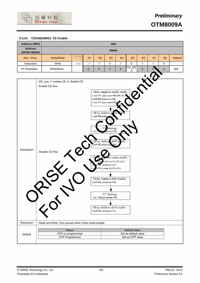
PPrreelliimmiinnaarryy
OTM8009A
© ORISE Technology Co., Ltd.
Proprietary & Confidential
162 FEB.22, 2012
Preliminary Version 0.8
5.3.61. CEEN(D680h): CE Enable
Address (MIPI) D6h
Address (SPI/I2C/MDDI)
D680h
Inst. / Para. Write/Read D[15:8
] D7 D6 D5 D4 D3 D2 D1 D0 Default
Instruction Write 00h 1 1 0 1 0 1 1 0
81 Parameter Write/Read 0 0 0 0 CE_EN
A 0 0 0 00h
Description
- CE_ena, 1: enable CE, 0: disable CE
- Enable CE flow
- Disable CE flow
Restriction - Read and Write, Only access when Orise mode enable.
Default
Status Default Value
OTP un-programmed Set as default value OTP Programmed Set as OTP value
ORISE Tec
h Con
fiden
tial
For IV
O Use
Only

PPrreelliimmiinnaarryy
OTM8009A
© ORISE Technology Co., Ltd.
Proprietary & Confidential
163 FEB.22, 2012
Preliminary Version 0.8
5.3.62. AIEEN(D700h): AIE Enable
Address (MIPI) D7h
Address (SPI/I2C/MDDI)
D700h
Inst. / Para. Write/Read D[15:8] D7 D6 D5 D4 D3 D2 D1 D0 Default
Instruction Write 00h 1 1 0 1 0 1 1 1
Parameter Write 0 0 0 0 AIE_EN
A AIE_SEL [2:0] 00h
Description
- AIE_ENA, 1: enable AIE, 0: disable AIE
- AIE_SEL [2:0]: AIE_SEL to select one Gamma setting from 8 settings, the gamma need been select by user manual.
Orise engineer mode enableCmd FFh parameter 80h,09h,01h
Cmd 00h parameter 80h
Cmd FFh parameter 80h,09h
Orise Address shift enableCmd 00h parameter 00h
AIE Gamma Curve selectCmd D7h parameter 1
AIE SettingsCmd C9h parameter (18 parameters)
Orise Address shift enableCmd 00h parameter 00h
AIE Gamma Curve selectCmd D7h parameter 00h
Orise Address shift enableCmd 00h parameter 00h
Restriction - Write, Only access when Orise mode enable.
Default
Status Default Value
OTP un-programmed No OTP Support OTP Programmed No OTP Support
ORISE Tec
h Con
fiden
tial
For IV
O Use
Only

PPrreelliimmiinnaarryy
OTM8009A
© ORISE Technology Co., Ltd.
Proprietary & Confidential
164 FEB.22, 2012
Preliminary Version 0.8
5.3.63. GVDDSET (D800h): GVDD/NGVDD
Address D8h
Address (SPI/I2C/MDDI)
D8001h ~ D802h (0x01st ~ 0x02th parameter)
Inst. / Para. Write/Read D[15:8] D7 D6 D5 D4 D3 D2 D1 D0 Default
Instruction Write 00h 1 1 0 1 1 0 0 0
1st Parameter Write/Read GVDD[7:0] 97h
2nd Parameter Write/Read NGVDD[7:0] 97h
Description
- GVDD[7:0] : GVDD Voltage Setting
GVDD[7:0] GVDD GVDD[7:0] GVDD GVDD[7:0] GVDD GVDD[7:0] GVDD GVDD[7:0] GVDD GVDD[7:0] GVDD GVDD[7:0] GVDD GVDD[7:0] GVDD0 3.1125 20 3.5125 40 3.9125 60 4.3125 80 4.7125 A0 5.1125 C0 5.5125 E0 5.91251 3.125 21 3.525 41 3.925 61 4.325 81 4.725 A1 5.125 C1 5.5125 E1 5.9252 3.1375 22 3.5375 42 3.9375 62 4.3375 82 4.7375 A2 5.1375 C2 5.5125 E2 5.93753 3.15 23 3.55 43 3.95 63 4.35 83 4.75 A3 5.15 C3 5.5125 E3 5.954 3.1625 24 3.5625 44 3.9625 64 4.3625 84 4.7625 A4 5.1625 C4 5.5125 E4 5.96255 3.175 25 3.575 45 3.975 65 4.375 85 4.775 A5 5.175 C5 5.5125 E5 5.9756 3.1875 26 3.5875 46 3.9875 66 4.3875 86 4.7875 A6 5.1875 C6 5.5125 E6 5.98757 3.2 27 3.6 47 4 67 4.4 87 4.8 A7 5.2 C7 5.5125 E7 68 3.2125 28 3.6125 48 4.0125 68 4.4125 88 4.8125 A8 5.2125 C8 5.5125 E8 6.01259 3.225 29 3.625 49 4.025 69 4.425 89 4.825 A9 5.225 C9 5.5125 E9 6.025A 3.2375 2A 3.6375 4A 4.0375 6A 4.4375 8A 4.8375 AA 5.2375 CA 5.5125 EA 6.0375B 3.25 2B 3.65 4B 4.05 6B 4.45 8B 4.85 AB 5.25 CB 5.5125 EB 6.05C 3.2625 2C 3.6625 4C 4.0625 6C 4.4625 8C 4.8625 AC 5.2625 CC 5.5125 EC 6.0625D 3.275 2D 3.675 4D 4.075 6D 4.475 8D 4.875 AD 5.275 CD 5.5125 ED 6.075E 3.2875 2E 3.6875 4E 4.0875 6E 4.4875 8E 4.8875 AE 5.2875 CE 5.5125 EE 6.0875F 3.3 2F 3.7 4F 4.1 6F 4.5 8F 4.9 AF 5.3 CF 5.5125 EF 6.110 3.3125 30 3.7125 50 4.1125 70 4.5125 90 4.9125 B0 5.3125 D0 5.5125 F0 6.112511 3.325 31 3.725 51 4.125 71 4.525 91 4.925 B1 5.325 D1 5.5125 F1 6.12512 3.3375 32 3.7375 52 4.1375 72 4.5375 92 4.9375 B2 5.3375 D2 5.5125 F2 6.137513 3.35 33 3.75 53 4.15 73 4.55 93 4.95 B3 5.35 D3 5.5125 F3 6.1514 3.3625 34 3.7625 54 4.1625 74 4.5625 94 4.9625 B4 5.3625 D4 5.5125 F4 6.162515 3.375 35 3.775 55 4.175 75 4.575 95 4.975 B5 5.375 D5 5.5125 F5 6.17516 3.3875 36 3.7875 56 4.1875 76 4.5875 96 4.9875 B6 5.3875 D6 5.5125 F6 6.187517 3.4 37 3.8 57 4.2 77 4.6 97 5 B7 5.4 D7 5.5125 F7 6.218 3.4125 38 3.8125 58 4.2125 78 4.6125 98 5.0125 B8 5.4125 D8 5.5125 F8 6.212519 3.425 39 3.825 59 4.225 79 4.625 99 5.025 B9 5.425 D9 5.5125 F9 6.2251A 3.4375 3A 3.8375 5A 4.2375 7A 4.6375 9A 5.0375 BA 5.4375 DA 5.5125 FA 6.23751B 3.45 3B 3.85 5B 4.25 7B 4.65 9B 5.05 BB 5.45 DB 5.5125 FB 6.251C 3.4625 3C 3.8625 5C 4.2625 7C 4.6625 9C 5.0625 BC 5.4625 DC 5.5125 FC 6.26251D 3.475 3D 3.875 5D 4.275 7D 4.675 9D 5.075 BD 5.475 DD 5.5125 FD 6.2751E 3.4875 3E 3.8875 5E 4.2875 7E 4.6875 9E 5.0875 BE 5.4875 DE 5.5125 FE 6.28751F 3.5 3F 3.9 5F 4.3 7F 4.7 9F 5.1 BF 5.5 DF 5.5125 FF 6.3
- NGVDD[7:0] : NGVDD Voltage Setting
NGVDD[7:0 NGVDD NGVDD[7:0 NGVDD NGVDD[7:0 NGVDD NGVDD[7:0 NGVDD NGVDD[7:0 NGVDD NGVDD[7:0 NGVDD NGVDD[7:0 NGVDD NGVDD[7:0 NGVDD0 -3.1125 20 -3.5125 40 -3.9125 60 -4.3125 80 -4.7125 A0 -5.1125 C0 -5.5125 E0 -5.91251 -3.125 21 -3.525 41 -3.925 61 -4.325 81 -4.725 A1 -5.125 C1 -5.525 E1 -5.9252 -3.1375 22 -3.5375 42 -3.9375 62 -4.3375 82 -4.7375 A2 -5.1375 C2 -5.5375 E2 -5.93753 -3.15 23 -3.55 43 -3.95 63 -4.35 83 -4.75 A3 -5.15 C3 -5.55 E3 -5.954 -3.1625 24 -3.5625 44 -3.9625 64 -4.3625 84 -4.7625 A4 -5.1625 C4 -5.5625 E4 -5.96255 -3.175 25 -3.575 45 -3.975 65 -4.375 85 -4.775 A5 -5.175 C5 -5.575 E5 -5.9756 -3.1875 26 -3.5875 46 -3.9875 66 -4.3875 86 -4.7875 A6 -5.1875 C6 -5.5875 E6 -5.98757 -3.2 27 -3.6 47 -4 67 -4.4 87 -4.8 A7 -5.2 C7 -5.6 E7 -68 -3.2125 28 -3.6125 48 -4.0125 68 -4.4125 88 -4.8125 A8 -5.2125 C8 -5.6125 E8 -6.01259 -3.225 29 -3.625 49 -4.025 69 -4.425 89 -4.825 A9 -5.225 C9 -5.625 E9 -6.025A -3.2375 2A -3.6375 4A -4.0375 6A -4.4375 8A -4.8375 AA -5.2375 CA -5.6375 EA -6.0375B -3.25 2B -3.65 4B -4.05 6B -4.45 8B -4.85 AB -5.25 CB -5.65 EB -6.05C -3.2625 2C -3.6625 4C -4.0625 6C -4.4625 8C -4.8625 AC -5.2625 CC -5.6625 EC -6.0625D -3.275 2D -3.675 4D -4.075 6D -4.475 8D -4.875 AD -5.275 CD -5.675 ED -6.075E -3.2875 2E -3.6875 4E -4.0875 6E -4.4875 8E -4.8875 AE -5.2875 CE -5.6875 EE -6.0875F -3.3 2F -3.7 4F -4.1 6F -4.5 8F -4.9 AF -5.3 CF -5.7 EF -6.110 -3.3125 30 -3.7125 50 -4.1125 70 -4.5125 90 -4.9125 B0 -5.3125 D0 -5.7125 F0 -6.112511 -3.325 31 -3.725 51 -4.125 71 -4.525 91 -4.925 B1 -5.325 D1 -5.725 F1 -6.12512 -3.3375 32 -3.7375 52 -4.1375 72 -4.5375 92 -4.9375 B2 -5.3375 D2 -5.7375 F2 -6.137513 -3.35 33 -3.75 53 -4.15 73 -4.55 93 -4.95 B3 -5.35 D3 -5.75 F3 -6.1514 -3.3625 34 -3.7625 54 -4.1625 74 -4.5625 94 -4.9625 B4 -5.3625 D4 -5.7625 F4 -6.162515 -3.375 35 -3.775 55 -4.175 75 -4.575 95 -4.975 B5 -5.375 D5 -5.775 F5 -6.17516 -3.3875 36 -3.7875 56 -4.1875 76 -4.5875 96 -4.9875 B6 -5.3875 D6 -5.7875 F6 -6.187517 -3.4 37 -3.8 57 -4.2 77 -4.6 97 -5 B7 -5.4 D7 -5.8 F7 -6.218 -3.4125 38 -3.8125 58 -4.2125 78 -4.6125 98 -5.0125 B8 -5.4125 D8 -5.8125 F8 -6.212519 -3.425 39 -3.825 59 -4.225 79 -4.625 99 -5.025 B9 -5.425 D9 -5.825 F9 -6.2251A -3.4375 3A -3.8375 5A -4.2375 7A -4.6375 9A -5.0375 BA -5.4375 DA -5.8375 FA -6.23751B -3.45 3B -3.85 5B -4.25 7B -4.65 9B -5.05 BB -5.45 DB -5.85 FB -6.251C -3.4625 3C -3.8625 5C -4.2625 7C -4.6625 9C -5.0625 BC -5.4625 DC -5.8625 FC -6.26251D -3.475 3D -3.875 5D -4.275 7D -4.675 9D -5.075 BD -5.475 DD -5.875 FD -6.2751E -3.4875 3E -3.8875 5E -4.2875 7E -4.6875 9E -5.0875 BE -5.4875 DE -5.8875 FE -6.28751F -3.5 3F -3.9 5F -4.3 7F -4.7 9F -5.1 BF -5.5 DF -5.9 FF -6.3
ORISE Tec
h Con
fiden
tial
For IV
O Use
Only

PPrreelliimmiinnaarryy
OTM8009A
© ORISE Technology Co., Ltd.
Proprietary & Confidential
165 FEB.22, 2012
Preliminary Version 0.8
Restriction - Read and Write, Only access when CMD2 mode enable.
Default
Status Default Value
OTP un-programmed Set as default value OTP programmed Set as OTP value
5.3.64. VCOMDC (D900h): VCOM voltage setting
Address D9h
Address (SPI/I2C/MDDI)
D900h
Inst. / Para. Write/Read D[15:8] D7 D6 D5 D4 D3 D2 D1 D0 Default
Instruction Write 00h 1 1 0 1 1 0 0 1
1st Parameter Write/Read VCOMDC 39h
Description
- VCOMDC represent the VCOMDC voltage
Setting table please see below.
VCOM[7:0] VCOM VCOM[7:0] VCOM VCOM[7:0] VCOM VCOM[7:0] VCOM VCOM[7:0] VCOM VCOM[7:0] VCOM VCOM[7:0] VCOM VCOM[7:0] VCOM0 0.0000 20 -0.6875 40 -1.0875 60 -1.4875 80 -1.8875 A0 -2.2875 C0 -2.6875 E0 -3.08751 -0.3000 21 -0.7000 41 -1.1000 61 -1.5000 81 -1.9000 A1 -2.3000 C1 -2.7000 E1 -3.10002 -0.3125 22 -0.7125 42 -1.1125 62 -1.5125 82 -1.9125 A2 -2.3125 C2 -2.7125 E2 -3.11253 -0.3250 23 -0.7250 43 -1.1250 63 -1.5250 83 -1.9250 A3 -2.3250 C3 -2.7250 E3 -3.12504 -0.3375 24 -0.7375 44 -1.1375 64 -1.5375 84 -1.9375 A4 -2.3375 C4 -2.7375 E4 -3.13755 -0.3500 25 -0.7500 45 -1.1500 65 -1.5500 85 -1.9500 A5 -2.3500 C5 -2.7500 E5 -3.15006 -0.3625 26 -0.7625 46 -1.1625 66 -1.5625 86 -1.9625 A6 -2.3625 C6 -2.7625 E6 -3.16257 -0.3750 27 -0.7750 47 -1.1750 67 -1.5750 87 -1.9750 A7 -2.3750 C7 -2.7750 E7 -3.17508 -0.3875 28 -0.7875 48 -1.1875 68 -1.5875 88 -1.9875 A8 -2.3875 C8 -2.7875 E8 -3.18759 -0.4000 29 -0.8000 49 -1.2000 69 -1.6000 89 -2.0000 A9 -2.4000 C9 -2.8000 E9 -3.2000A -0.4125 2A -0.8125 4A -1.2125 6A -1.6125 8A -2.0125 AA -2.4125 CA -2.8125 EA -3.2125B -0.4250 2B -0.8250 4B -1.2250 6B -1.6250 8B -2.0250 AB -2.4250 CB -2.8250 EB -3.2250C -0.4375 2C -0.8375 4C -1.2375 6C -1.6375 8C -2.0375 AC -2.4375 CC -2.8375 EC -3.2375D -0.4500 2D -0.8500 4D -1.2500 6D -1.6500 8D -2.0500 AD -2.4500 CD -2.8500 ED -3.2500E -0.4625 2E -0.8625 4E -1.2625 6E -1.6625 8E -2.0625 AE -2.4625 CE -2.8625 EE -3.2625F -0.4750 2F -0.8750 4F -1.2750 6F -1.6750 8F -2.0750 AF -2.4750 CF -2.8750 EF -3.275010 -0.4875 30 -0.8875 50 -1.2875 70 -1.6875 90 -2.0875 B0 -2.4875 D0 -2.8875 F0 -3.287511 -0.5000 31 -0.9000 51 -1.3000 71 -1.7000 91 -2.1000 B1 -2.5000 D1 -2.9000 F1 -3.300012 -0.5125 32 -0.9125 52 -1.3125 72 -1.7125 92 -2.1125 B2 -2.5125 D2 -2.9125 F2 -3.312513 -0.5250 33 -0.9250 53 -1.3250 73 -1.7250 93 -2.1250 B3 -2.5250 D3 -2.9250 F3 -3.325014 -0.5375 34 -0.9375 54 -1.3375 74 -1.7375 94 -2.1375 B4 -2.5375 D4 -2.9375 F4 -3.337515 -0.5500 35 -0.9500 55 -1.3500 75 -1.7500 95 -2.1500 B5 -2.5500 D5 -2.9500 F5 -3.350016 -0.5625 36 -0.9625 56 -1.3625 76 -1.7625 96 -2.1625 B6 -2.5625 D6 -2.9625 F6 -3.362517 -0.5750 37 -0.9750 57 -1.3750 77 -1.7750 97 -2.1750 B7 -2.5750 D7 -2.9750 F7 -3.375018 -0.5875 38 -0.9875 58 -1.3875 78 -1.7875 98 -2.1875 B8 -2.5875 D8 -2.9875 F8 -3.387519 -0.6000 39 -1.0000 59 -1.4000 79 -1.8000 99 -2.2000 B9 -2.6000 D9 -3.0000 F9 -3.40001A -0.6125 3A -1.0125 5A -1.4125 7A -1.8125 9A -2.2125 BA -2.6125 DA -3.0125 FA -3.41251B -0.6250 3B -1.0250 5B -1.4250 7B -1.8250 9B -2.2250 BB -2.6250 DB -3.0250 FB -3.42501C -0.6375 3C -1.0375 5C -1.4375 7C -1.8375 9C -2.2375 BC -2.6375 DC -3.0375 FC -3.43751D -0.6500 3D -1.0500 5D -1.4500 7D -1.8500 9D -2.2500 BD -2.6500 DD -3.0500 FD -3.45001E -0.6625 3E -1.0625 5E -1.4625 7E -1.8625 9E -2.2625 BE -2.6625 DE -3.0625 FE -3.46251F -0.6750 3F -1.0750 5F -1.4750 7F -1.8750 9F -2.2750 BF -2.6750 DF -3.0750 FF -3.4750
Restriction - Read and Write, Only access when CMD2 mode enable.
Default
Status Default Value
OTP un-programmed Set as default value OTP Programmed Set as OTP value
ORISE Tec
h Con
fiden
tial
For IV
O Use
Only

PPrreelliimmiinnaarryy
OTM8009A
© ORISE Technology Co., Ltd.
Proprietary & Confidential
166 FEB.22, 2012
Preliminary Version 0.8
5.3.65. GMCT2.2P (E100h): Gamma Correction Characteristics Setting (2.2 + )
Address E1h
Address (SPI/I2C/MDDI)
E100h ~ E10Fh (0x01st ~ 0x10th Parameter)
Inst. / Para. Write/Read D[15:8] D7 D6 D5 D4 D3 D2 D1 D0 Default
Instruction Write 00h 1 1 1 0 0 0 0 1 E1h
1st Parameter Write/Read 0 0 G22P1 G22P1 G22P1 G22P1 G22P1 G22P1 09h 2nd Parameter Write/Read 0 0 G22P2 G22P2 G22P2 G22P2 G22P2 G22P2 11h 3rd Parameter Write/Read 0 0 G22P3 G22P3 G22P3 G22P3 G22P3 G22P3 17h 4th Parameter Write/Read 0 0 0 G22P4 G22P4 G22P4 G22P4 G22P4 0Dh 5th Parameter Write/Read 0 0 0 G22P5 G22P5 G22P5 G22P5 G22P5 06h 6th Parameter Write/Read 0 0 0 G22P6 G22P6 G22P6 G22P6 G22P6 0Eh 7th Parameter Write/Read 0 0 0 0 G22P7 G22P7 G22P7 G22P7 0Ah 8th Parameter Write/Read 0 0 0 0 G22P8 G22P8 G22P8 G22P8 08h 9th Parameter Write/Read 0 0 0 0 G22P9 G22P9 G22P9 G22P9 05h
10th Parameter Write/Read 0 0 0 0 G22P
10 G22P
10 G22P
10 G22P
10 09h
11st Parameter Write/Read 0 0 0 G22P
11 G22P
11 G22P
11 G22P
11 G22P
11 0Dh
12nd Parameter Write/Read 0 0 0 G22P
12 G22P
12 G22P
12 G22P
12 G22P
12 07h
13rd Parameter Write/Read 0 0 0 G22P
13 G22P
13 G22P
13 G22P
13 G22P
13 0Eh
14th Parameter Write/Read 0 0 G22P
14 G22P
14 G22P
14 G22P
14 G22P
14 G22P
140Eh
15th Parameter Write/Read 0 0 G22P
15 G22P
15 G22P
15 G22P
15 G22P
15 G22P
15 0Ah
16th Parameter Write/Read 0 0 G22P
16 G22P
16 G22P
16 G22P
16 G22P
16 G22P
16 05h
Description
- Gamma adjustment for 2.2 positive setting.
Restriction - Read and Write, Only access when Orise mode enable.
Default
Status Default Value
OTP un-programmed Set as default value OTP Programmed Set as OTP value
Power ON
Hardware Rest
Enable ORISE command modeCMD=0xFF, DAT=0x80,0x09,0x01CMD=0x00, DAT=0x80CMD=0xFF, DAT=0x80,0x09
Address shift CMD=0x00, DAT=0x00
Set GammaE1h/E2h/E3h/E4h/E5h/E6h/E7h/E8h
Set End CMD=0x00, DAT=0x00
Address shift CMD=0x00, DAT=0x00
Read Gamma parameterE1h/E2h/E3h/E4h/E5h/E6h/E7h/E8h
Read End CMD=0x00, DAT=0x00
Wait 5ms
ORISE Tec
h Con
fiden
tial
For IV
O Use
Only

PPrreelliimmiinnaarryy
OTM8009A
© ORISE Technology Co., Ltd.
Proprietary & Confidential
167 FEB.22, 2012
Preliminary Version 0.8
5.3.66. GMCT2.2N (E200h): Gamma Correction Characteristics Setting (2.2 - )
Address E2h
Address (SPI/I2C/MDDI)
E200h ~ E20Fh (0x01st ~ 0x10th Parameter)
Inst. / Para. Write/Read D[15:8] D7 D6 D5 D4 D3 D2 D1 D0 Default
Instruction Write 00h 1 1 1 0 0 0 1 0 E2h
1st Parameter Write/Read 0 0 G22N1 G22N1 G22N1 G22N 1 G22N 1 G22N 1 09h 2nd Parameter Write/Read 0 0 G22N2 G22N2 G22N2 G22N2 G22N2 G22N2 11h 3rd Parameter Write/Read 0 0 G22N3 G22N3 G22N3 G22N3 G22N3 G22N3 17h 4th Parameter Write/Read 0 0 0 G22N4 G22N4 G22N4 G22N4 G22N4 0Dh 5th Parameter Write/Read 0 0 0 G22N5 G22N5 G22N5 G22N5 G22N5 06h 6th Parameter Write/Read 0 0 0 G22N6 G22N6 G22N6 G22N6 G22N6 0Eh 7th Parameter Write/Read 0 0 0 0 G22N7 G22N7 G22N7 G22N7 0Ah 8th Parameter Write/Read 0 0 0 0 G22N8 G22N8 G22N8 G22N8 08h 9th Parameter Write/Read 0 0 0 0 G22N9 G22N9 G22N9 G22N9 05h
10th Parameter Write/Read 0 0 0 0 G22N
10 G22N
10 G22N
10 G22N
10 09h
11st Parameter Write/Read 0 0 0 G22N
11 G22N
11 G22N
11 G22N
11 G22N
11 0Dh
12nd Parameter Write/Read 0 0
0 G22N
12 G22N
12 G22N
12 G22N
12 G22N
12 07h
13rd Parameter Write/Read 0 0
0 G22N
13 G22N
13 G22N
13 G22N
13 G22N
13 0Eh
14th Parameter Write/Read 0 0 G22N
14 G22N
14 G22N
14 G22N
14 G22N
14 G22N
14 0Eh
15th Parameter Write/Read 0 0 G22N
15 G22N
15 G22N
15 G22N
15 G22N
15 G22N
15 0Ah
16th Parameter Write/Read 0 0 G22N
16 G22N
16 G22N
16 G22N
16 G22N
16 G22N
16 05h
Description
- Gamma adjustment for 2.2 negative setting.
Restriction - Read and Write, Only access when Orise mode enable.
Default
Status Default Value
OTP un-programmed Set as default value OTP Programmed Set as OTP value
ORISE Tec
h Con
fiden
tial
For IV
O Use
Only

PPrreelliimmiinnaarryy
OTM8009A
© ORISE Technology Co., Ltd.
Proprietary & Confidential
168 FEB.22, 2012
Preliminary Version 0.8
5.3.67. GMCT1.8P (E300h): Gamma Correction Characteristics Setting (1.8 + )
Address E3h
Address (SPI/I2C/MDDI)
E300h ~ E311h (0x01st ~ 0x10th Parameter)
Inst. / Para. Write/Read D[15:8] D7 D6 D5 D4 D3 D2 D1 D0 Default
Instruction Write 00h 1 1 1 0 0 0 1 1 E3h
1st Parameter Write 0 0 G18P1 G18P1 G18P1 G18P1 G18P1 G18P1 09h 2nd Parameter Write/Read 0 0 G18P2 G18P2 G18P2 G18P2 G18P2 G18P2 11h 3rd Parameter Write/Read 0 0 G18P3 G18P3 G18P3 G18P3 G18P3 G18P3 17h 4th Parameter Write/Read 0 0 0 G18P4 G18P4 G18P4 G18P4 G18P4 0Dh 5th Parameter Write/Read 0 0 0 G18P5 G18P5 G18P5 G18P5 G18P5 06h 6th Parameter Write/Read 0 0 0 G18P6 G18P6 G18P6 G18P6 G18P6 0Eh 7th Parameter Write/Read 0 0 0 0 G18P7 G18P7 G18P7 G18P7 0Ah 8th Parameter Write/Read 0 0 0 0 G18P8 G18P8 G18P8 G18P8 08h 9th Parameter Write/Read 0 0 0 0 G18P9 G18P9 G18P9 G18P9 05h
10th Parameter Write/Read 0 0 0 0 G18P
10 G18P
10 G18P
10 G18P
10 09h
11st Parameter Write/Read 0 0 0 G18P
11 G18P
11 G18P
11 G18P
11 G18P
11 0Dh
12nd Parameter Write/Read 0 0
0 G18P
12 G18P
12 G18P
12 G18P
12 G18P
12 07h
13rd Parameter Write/Read 0 0
0 G18P
13 G18P
13 G18P
13 G18P
13 G18P
13 0Eh
14th Parameter Write/Read 0 0 G18P
14 G18P
14 G18P
14 G18P
14 G18P
14 G18P14
0Eh
15th Parameter Write/Read 0 0 G18P
15 G18P
15 G18P
15 G18P
15 G18P
15 G18P
15 0Ah
16th Parameter Write/Read 0 0 G18P
16 G18P
16 G18P
16 G18P
16 G18P
16 G18P
16 05h
Description
- Gamma adjustment for 1.8 positive setting.
Restriction - Read and Write, Only access when Orise mode enable.
Default
Status Default Value
OTP un-programmed Set as default value OTP Programmed Set as OTP value
Power ON
Hardware Rest
Enable ORISE command modeCMD=0xFF, DAT=0x80,0x09,0x01CMD=0x00, DAT=0x80CMD=0xFF, DAT=0x80,0x09
Address shift CMD=0x00, DAT=0x00
Set GammaE1h/E2h/E3h/E4h/E5h/E6h/E7h/E8h
Set End CMD=0x00, DAT=0x00
Address shift CMD=0x00, DAT=0x00
Read Gamma parameterE1h/E2h/E3h/E4h/E5h/E6h/E7h/E8h
Read End CMD=0x00, DAT=0x00
Wait 5ms
ORISE Tec
h Con
fiden
tial
For IV
O Use
Only

PPrreelliimmiinnaarryy
OTM8009A
© ORISE Technology Co., Ltd.
Proprietary & Confidential
169 FEB.22, 2012
Preliminary Version 0.8
5.3.68. GMCT1.8N (E400h): Gamma Correction Characteristics Setting (1.8 - )
Address E4h
Address (SPI/I2C/MDDI)
E400h ~ E40Fh (0x01st ~ 0x10th Parameter)
Inst. / Para. Write/Read D[15:8] D7 D6 D5 D4 D3 D2 D1 D0 Default
Instruction Write 00h 1 1 1 0 0 1 0 0 E4h
1st Parameter Write/Read 0 0 G18N1 G18N1 G18N1 G18N1 G18N1 G18N1 09h 2nd Parameter Write/Read 0 0 G18N2 G18N2 G18N2 G18N2 G18N2 G18N2 11h 3rd Parameter Write/Read 0 0 G18N3 G18N3 G18N3 G18N3 G18N3 G18N3 17h 4th Parameter Write/Read 0 0 0 G18N4 G18N4 G18N4 G18N4 G18N4 0Dh 5th Parameter Write/Read 0 0 0 G18N5 G18N5 G18N5 G18N5 G18N5 06h 6th Parameter Write/Read 0 0 0 G18N6 G18N6 G18N6 G18N6 G18N6 0Eh 7th Parameter Write/Read 0 0 0 0 G18N7 G18N7 G18N7 G18N7 0Ah 8th Parameter Write/Read 0 0 0 0 G18N8 G18N8 G18N8 G18N8 08h 9th Parameter Write/Read 0 0 0 0 G18N9 G18N9 G18N9 G18N9 05h
10th Parameter Write/Read 0 0 0 0 G18N
10 G18N
10 G18N
10 G18N
10 09h
11st Parameter Write/Read 0 0 0 G18N
11 G18N
11 G18N
11 G18N
11 G18N
11 0Dh
12nd Parameter Write/Read 0 0
0 G18N
12 G18N
12 G18N
12 G18N
12 G18N
12 07h
13rd Parameter Write/Read 0 0
0 G18N
13 G18N
13 G18N
13 G18N
13 G18N
13 0Eh
14th Parameter Write/Read 0 0 G18N
14 G18N
14 G18N
14 G18N
14 G18N
14 G18N14
0Eh
15th Parameter Write/Read 0 0 G18N
15 G18N
15 G18N
15 G18N
15 G18N
15 G18N
15 0Ah
16th Parameter Write/Read 0 0 G18N
16 G18N
16 G18N
16 G18N
16 G18N
16 G18N
16 05h
Description
- Gamma adjustment for 1.8 negative setting.
Restriction - Read and Write, Only access when Orise mode enable.
Default
Status Default Value
OTP un-programmed Set as default value OTP Programmed Set as OTP value
ORISE Tec
h Con
fiden
tial
For IV
O Use
Only

PPrreelliimmiinnaarryy
OTM8009A
© ORISE Technology Co., Ltd.
Proprietary & Confidential
170 FEB.22, 2012
Preliminary Version 0.8
5.3.69. GMCT2.5P (E500h): Gamma Correction Characteristics Setting (2.5 + )
Address E5h
Address (SPI/I2C/MDDI)
E500h ~ E50Fh (0x01st ~ 0x10th Parameter)
Inst. / Para. Write/Read D[15:8] D7 D6 D5 D4 D3 D2 D1 D0 Default
Instruction Write 00h 1 1 1 0 0 1 0 1 E5h
1st Parameter Write/Read 0 0 G25P1 G25P1 G25P1 G25P1 G25P1 G25P1 09h 2nd Parameter Write/Read 0 0 G25P2 G25P2 G25P2 G25P2 G25P2 G25P2 11h 3rd Parameter Write/Read 0 0 G25P3 G25P3 G25P3 G25P3 G25P3 G25P3 17h 4th Parameter Write/Read 0 0 0 G25P4 G25P4 G25P4 G25P4 G25P4 0Dh 5th Parameter Write/Read 0 0 0 G25P5 G25P5 G25P5 G25P5 G25P5 06h 6th Parameter Write/Read 0 0 0 G25P6 G25P6 G25P6 G25P6 G25P6 0Eh 7th Parameter Write/Read 0 0 0 0 G25P7 G25P7 G25P7 G25P7 0Ah 8th Parameter Write/Read 0 0 0 0 G25P8 G25P8 G25P8 G25P8 08h 9th Parameter Write/Read 0 0 0 0 G25P9 G25P9 G25P9 G25P9 05h
10th Parameter Write/Read
0 0 0 0 G25P
10 G25P
10 G25P
10 G25P
10 09h
11st Parameter Write/Read
0 0 0 G25P
11 G25P
11 G25P
11 G25P
11 G25P
11 0Dh
12nd Parameter Write/Read
0 0
0 G25P
12 G25P
12 G25P
12 G25P
12 G25P
12 07h
13rd Parameter Write/Read
0 0
0 G25P
13 G25P
13 G25P
13 G25P
13 G25P
13 0Eh
14th Parameter Write/Read
0 0 G25P
14 G25P
14 G25P
14 G25P
14 G25P
14 G25P14
0Eh
15th Parameter Write/Read
0 0 G25P
15 G25P
15 G25P
15 G25P
15 G25P
15 G25P
15 0Ah
16th Parameter Write/Read
0 0 G25P
16 G25P
16 G25P
16 G25P
16 G25P
16 G25P
16 05h
Description
- Gamma adjustment for2.5 positive setting.
Restriction - Read and Write, Only access when Orise mode enable.
Default
Status Default Value
OTP un-programmed Set as default value OTP Programmed Set as OTP value
Power ON
Hardware Rest
Enable ORISE command modeCMD=0xFF, DAT=0x80,0x09,0x01CMD=0x00, DAT=0x80CMD=0xFF, DAT=0x80,0x09
Address shift CMD=0x00, DAT=0x00
Set GammaE1h/E2h/E3h/E4h/E5h/E6h/E7h/E8h
Set End CMD=0x00, DAT=0x00
Address shift CMD=0x00, DAT=0x00
Read Gamma parameterE1h/E2h/E3h/E4h/E5h/E6h/E7h/E8h
Read End CMD=0x00, DAT=0x00
Wait 5ms
ORISE Tec
h Con
fiden
tial
For IV
O Use
Only

PPrreelliimmiinnaarryy
OTM8009A
© ORISE Technology Co., Ltd.
Proprietary & Confidential
171 FEB.22, 2012
Preliminary Version 0.8
5.3.70. GMCT2.5N (E600h): Gamma Correction Characteristics Setting (2.5 - )
Address E6h
Address (SPI/I2C/MDDI)
E600h ~ E60Fh (0x01st ~ 0x10th Parameter)
Inst. / Para. Write/Read D[15:8] D7 D6 D5 D4 D3 D2 D1 D0 Default
Instruction Write 00h 1 1 1 0 0 1 1 0 E6h
1st Parameter Write/Read 0 0 G25N1 G25N1 G25N1 G25N1 G25N1 G25N1 09h 2nd Parameter Write/Read 0 0 G25N2 G25N2 G25N2 G25N2 G25N2 G25N2 11h 3rd Parameter Write/Read 0 0 G25N3 G25N3 G25N3 G25N3 G25N3 G25N3 17h 4th Parameter Write/Read 0 0 0 G25N4 G25N4 G25N4 G25N4 G25N4 0Dh 5th Parameter Write/Read 0 0 0 G25N5 G25N5 G25N5 G25N5 G25N5 06h 6th Parameter Write/Read 0 0 0 G25N6 G25N6 G25N6 G25N6 G25N6 0Eh 7th Parameter Write/Read 0 0 0 0 G25N7 G25N7 G25N7 G25N7 0Ah 8th Parameter Write/Read 0 0 0 0 G25N8 G25N8 G25N8 G25N8 08h 9th Parameter Write/Read 0 0 0 0 G25N9 G25N9 G25N9 G25N9 05h
10th Parameter Write/Read 0 0 0 0 G25N
10 G25N
10 G25N
10 G25N
10 09h
11st Parameter Write/Read 0 0 0 G25N
11 G25N
11 G25N
11 G25N
11 G25N
11 0Dh
12nd Parameter Write/Read 0 0
0 G25N
12 G25N
12 G25N
12 G25N
12 G25N
12 07h
13rd Parameter Write/Read 0 0
0 G25N
13 G25N
13 G25N
13 G25N
13 G25N
13 0Eh
14th Parameter Write/Read 0 0 G25N
14 G25N
14 G25N
14 G25N
14 G25N
14 G25N14
0Eh
15th Parameter Write/Read 0 0 G25N
15 G25N
15 G25N
15 G25N
15 G25N
15 G25N
15 0Ah
16th Parameter Write/Read 0 0 G25N
16 G25N
16 G25N
16 G25N
16 G25N
16 G25N
16 05h
Description
- Gamma adjustment for 2.5 negative setting.
Restriction - Read and Write, Only access when Orise mode enable.
Default
Status Default Value
OTP un-programmed Set as default value OTP Programmed Set as OTP value
Power ON
Hardware Rest
Enable ORISE command modeCMD=0xFF, DAT=0x80,0x09,0x01CMD=0x00, DAT=0x80CMD=0xFF, DAT=0x80,0x09
Address shift CMD=0x00, DAT=0x00
Set GammaE1h/E2h/E3h/E4h/E5h/E6h/E7h/E8h
Set End CMD=0x00, DAT=0x00
Address shift CMD=0x00, DAT=0x00
Read Gamma parameterE1h/E2h/E3h/E4h/E5h/E6h/E7h/E8h
Read End CMD=0x00, DAT=0x00
Wait 5ms
ORISE Tec
h Con
fiden
tial
For IV
O Use
Only
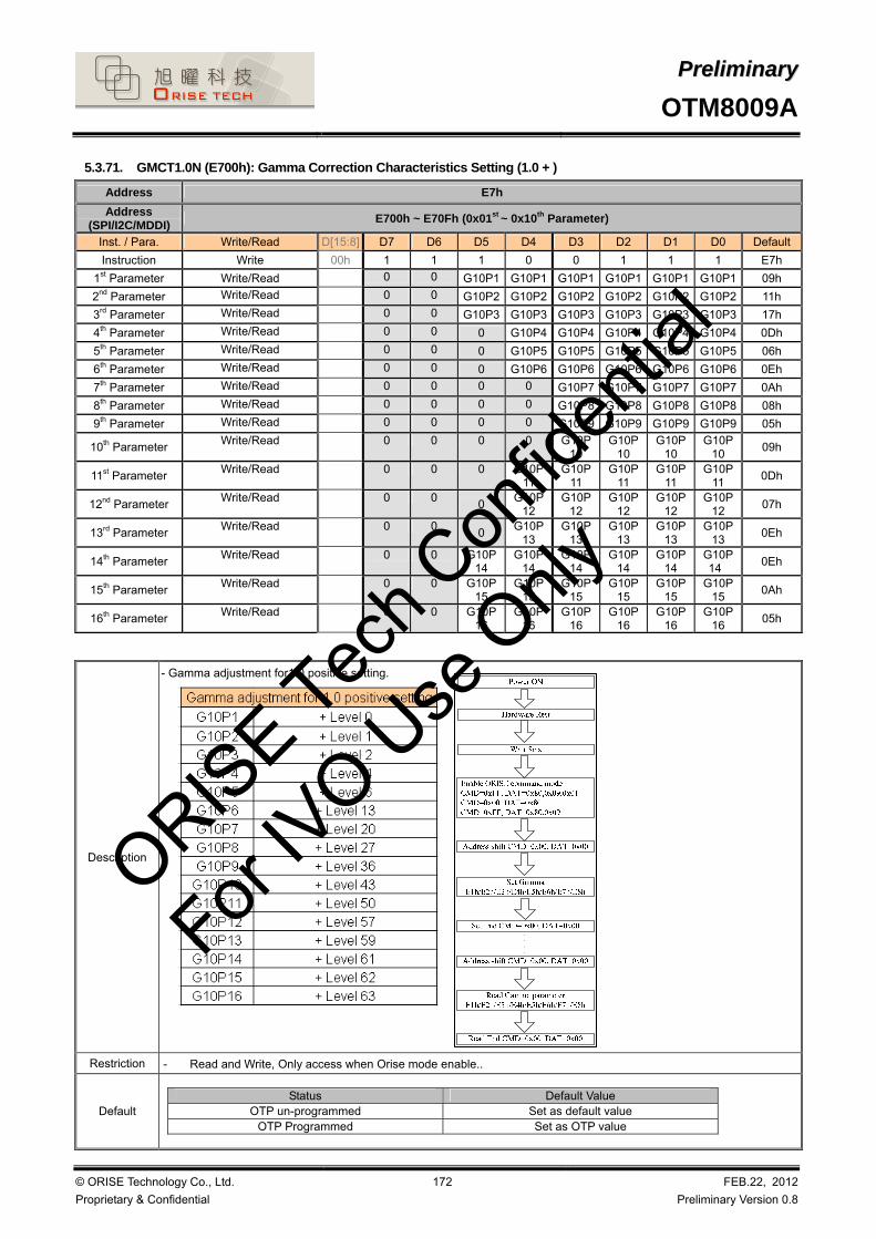
PPrreelliimmiinnaarryy
OTM8009A
© ORISE Technology Co., Ltd.
Proprietary & Confidential
172 FEB.22, 2012
Preliminary Version 0.8
5.3.71. GMCT1.0N (E700h): Gamma Correction Characteristics Setting (1.0 + )
Address E7h
Address (SPI/I2C/MDDI)
E700h ~ E70Fh (0x01st ~ 0x10th Parameter)
Inst. / Para. Write/Read D[15:8] D7 D6 D5 D4 D3 D2 D1 D0 Default
Instruction Write 00h 1 1 1 0 0 1 1 1 E7h
1st Parameter Write/Read 0 0 G10P1 G10P1 G10P1 G10P1 G10P1 G10P1 09h 2nd Parameter Write/Read 0 0 G10P2 G10P2 G10P2 G10P2 G10P2 G10P2 11h 3rd Parameter Write/Read 0 0 G10P3 G10P3 G10P3 G10P3 G10P3 G10P3 17h 4th Parameter Write/Read 0 0 0 G10P4 G10P4 G10P4 G10P4 G10P4 0Dh 5th Parameter Write/Read 0 0 0 G10P5 G10P5 G10P5 G10P5 G10P5 06h 6th Parameter Write/Read 0 0 0 G10P6 G10P6 G10P6 G10P6 G10P6 0Eh 7th Parameter Write/Read 0 0 0 0 G10P7 G10P7 G10P7 G10P7 0Ah 8th Parameter Write/Read 0 0 0 0 G10P8 G10P8 G10P8 G10P8 08h 9th Parameter Write/Read 0 0 0 0 G10P9 G10P9 G10P9 G10P9 05h
10th Parameter Write/Read
0 0 0 0 G10P
10 G10P
10 G10P
10 G10P
10 09h
11st Parameter Write/Read
0 0 0 G10P
11 G10P
11 G10P
11 G10P
11 G10P
11 0Dh
12nd Parameter Write/Read
0 0
0 G10P
12 G10P
12 G10P
12 G10P
12 G10P
12 07h
13rd Parameter Write/Read
0 0
0 G10P
13 G10P
13 G10P
13 G10P
13 G10P
13 0Eh
14th Parameter Write/Read
0 0 G10P
14 G10P
14 G10P
14 G10P
14 G10P
14 G10P14
0Eh
15th Parameter Write/Read
0 0 G10P
15 G10P
15 G10P
15 G10P
15 G10P
15 G10P
15 0Ah
16th Parameter Write/Read
0 0 G10P
16 G10P
16 G10P
16 G10P
16 G10P
16 G10P
16 05h
Description
- Gamma adjustment for1.0 positive setting.
Restriction - Read and Write, Only access when Orise mode enable..
Default
Status Default Value
OTP un-programmed Set as default value OTP Programmed Set as OTP value
ORISE Tec
h Con
fiden
tial
For IV
O Use
Only

PPrreelliimmiinnaarryy
OTM8009A
© ORISE Technology Co., Ltd.
Proprietary & Confidential
173 FEB.22, 2012
Preliminary Version 0.8
5.3.72. GMCT1.0N (E800h): Gamma Correction Characteristics Setting (1.0 - )
Address E8h
Address (SPI/I2C/MDDI)
E800h ~ E80Fh (0x01st ~ 0x10th Parameter)
Inst. / Para. Write/Read D[15:8] D7 D6 D5 D4 D3 D2 D1 D0 Default
Instruction Write 00h 1 1 1 0 1 0 0 0 E8h
1st Parameter Write/Read 0 0 G10N1 G10N1 G10N1 G10N1 G10N1 G10N1 09h 2nd Parameter Write/Read 0 0 G10N2 G10N2 G10N2 G10N2 G10N2 G10N2 11h 3rd Parameter Write/Read 0 0 G10N3 G10N3 G10N3 G10N3 G10N3 G10N3 17h 4th Parameter Write/Read 0 0 0 G10N4 G10N4 G10N4 G10N4 G10N4 0Dh 5th Parameter Write/Read 0 0 0 G10N5 G10N5 G10N5 G10N5 G10N5 06h 6th Parameter Write/Read 0 0 0 G10N6 G10N6 G10N6 G10N6 G10N6 0Eh 7th Parameter Write/Read 0 0 0 0 G10N7 G10N7 G10N7 G10N7 0Ah 8th Parameter Write/Read 0 0 0 0 G10N8 G10N8 G10N8 G10N8 08h 9th Parameter Write/Read 0 0 0 0 G10N9 G10N9 G10N9 G10N9 05h
10th Parameter Write/Read 0 0 0 0 G10N
10 G10N
10 G10N
10 G10N
10 09h
11st Parameter Write/Read 0 0 0 G10N
11 G10N
11 G10N
11 G10N
11 G10N
11 0Dh
12nd Parameter Write/Read 0 0
0 G10N
12 G10N
12 G10N
12 G10N
12 G10N
12 07h
13rd Parameter Write/Read 0 0
0 G10N
13 G10N
13 G10N
13 G10N
13 G10N
13 0Eh
14th Parameter Write/Read 0 0 G10N
14 G10N
14 G10N
14 G10N
14 G10N
14 G10N14
0Eh
15th Parameter Write/Read 0 0 G10N
15 G10N
15 G10N
15 G10N
15 G10N
15 G10N
15 0Ah
16th Parameter Write/Read 0 0 G10N
16 G10N
16 G10N
16 G10N
16 G10N
16 G10N
16 05h
Description
- Gamma adjustment for1.0 negative setting.
Restriction - Read and Write, Only access when Orise mode enable.
Default
Status Default Value
OTP un-programmed Set as default value OTP Programmed Set as OTP value
Power ON
Hardware Rest
Enable ORISE command modeCMD=0xFF, DAT=0x80,0x09,0x01CMD=0x00, DAT=0x80CMD=0xFF, DAT=0x80,0x09
Address shift CMD=0x00, DAT=0x00
Set GammaE1h/E2h/E3h/E4h/E5h/E6h/E7h/E8h
Set End CMD=0x00, DAT=0x00
Address shift CMD=0x00, DAT=0x00
Read Gamma parameterE1h/E2h/E3h/E4h/E5h/E6h/E7h/E8h
Read End CMD=0x00, DAT=0x00
Wait 5ms
ORISE Tec
h Con
fiden
tial
For IV
O Use
Only

PPrreelliimmiinnaarryy
OTM8009A
© ORISE Technology Co., Ltd.
Proprietary & Confidential
174 FEB.22, 2012
Preliminary Version 0.8
5.3.73. NVMIN (EB00h): NV Memory Write Mode
Address EBh
Address (SPI/I2C/MDDI)
EB00h(0x01st Parameter)
Inst. / Para. Write/Read D[15:8] D7 D6 D5 D4 D3 D2 D1 D0 Default
Instruction Write 00h 1 1 1 0 1 0 1 1 EBh
Parameter Write 0 0 0 0 0 0 0 NVM_P
GM00h
Description
-NVM_PGM: NVM programming Function
NVM_PGM NVM programming Function
0 Disable
1 Enable
Restriction Only access when Orise mode enable.
Default
Status Default Value
OTP un-programmed No OTP Support OTP Programmed No OTP Support
ORISE Tec
h Con
fiden
tial
For IV
O Use
Only

PPrreelliimmiinnaarryy
OTM8009A
© ORISE Technology Co., Ltd.
Proprietary & Confidential
175 FEB.22, 2012
Preliminary Version 0.8
5.3.74. DGAMR (EC00h): Digital Gamma Correction Characteristics Setting (Red):
Address ECh
Address (SPI/I2C/MDDI)
EC00h ~ EC20h (0x01st ~ 0x21st Parameter)
Inst. / Para. Write/Read D[15:8] D7 D6 D5 D4 D3 D2 D1 D0 Default
Instruction Write 00h 1 1 1 0 1 1 0 0 ECh
1st Parameter Write/Read DGR2 DGR2 DGR2 DGR2 DGR1 DGR1 DGR1 DGR1 40h
2nd Parameter Write/Read DGR4 DGR4 DGR4 DGR4 DGR3 DGR3 DGR3 DGR3 44h
3rd Parameter Write/Read DGR6 DGR6 DGR6 DGR6 DGR5 DGR5 DGR5 DGR5 44h
: Write/Read : :
31st Parameter Write/Read DGR62 DGR62 DGR62 DGR62 DGR61 DGR61 DGR61 DGR61 44h
32nd Parameter Write/Read DGR64 DGR64 DGR64 DGR64 DGR63 DGR63 DGR63 DGR63 44h
33rd Parameter Write/Read 0 0 0 0 DGR65 DGR65 DGR65 DGR65 04h
Description
- Command ECh totally has 33 parameters, these parameters are settings for Digital gamma Red curve
- Gamma adjustment for Red setting.
Power ON
Hardware Rest
Enable ORISE command modeCMD=0xFF, DAT=0x80,0x09,0x01CMD=0x00, DAT=0x80CMD=0xFF, DAT=0x80,0x09
Address shift CMD=0x00, DAT=0x00
Set GammaEch/Edh/EEh
Set End CMD=0x00, DAT=0x00
Address shift CMD=0x00, DAT=0x00
Read Gamma parameterEch/Edh/EEh
Read End CMD=0x00, DAT=0x00
Wait 5ms
Restriction - Read and Write, Only access when Orise mode enable.
Default
Status Default Value
OTP un-programmed Set as default value OTP Programmed Set as OTP value
ORISE Tec
h Con
fiden
tial
For IV
O Use
Only
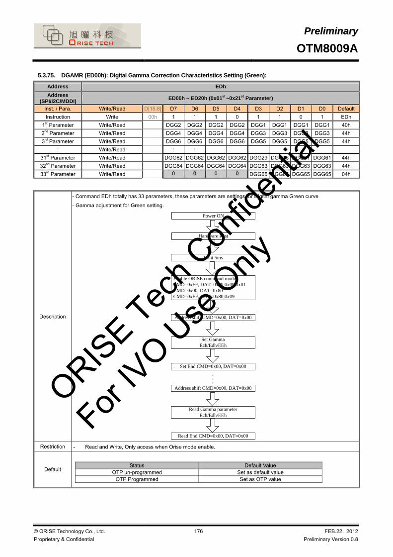
PPrreelliimmiinnaarryy
OTM8009A
© ORISE Technology Co., Ltd.
Proprietary & Confidential
176 FEB.22, 2012
Preliminary Version 0.8
5.3.75. DGAMR (ED00h): Digital Gamma Correction Characteristics Setting (Green):
Address EDh
Address (SPI/I2C/MDDI)
ED00h ~ ED20h (0x01st ~0x21st Parameter)
Inst. / Para. Write/Read D[15:8] D7 D6 D5 D4 D3 D2 D1 D0 Default
Instruction Write 00h 1 1 1 0 1 1 0 1 EDh
1st Parameter Write/Read DGG2 DGG2 DGG2 DGG2 DGG1 DGG1 DGG1 DGG1 40h
2nd Parameter Write/Read DGG4 DGG4 DGG4 DGG4 DGG3 DGG3 DGG3 DGG3 44h
3rd Parameter Write/Read DGG6 DGG6 DGG6 DGG6 DGG5 DGG5 DGG5 DGG5 44h
: Write/Read : :
31st Parameter Write/Read DGG62 DGG62 DGG62 DGG62 DGG29 DGG16 DGG61 DGG61 44h
32nd Parameter Write/Read DGG64 DGG64 DGG64 DGG64 DGG63 DGG63 DGG63 DGG63 44h
33rd Parameter Write/Read 0 0 0 0 DGG65 DGG65 DGG65 DGG65 04h
Description
- Command EDh totally has 33 parameters, these parameters are settings for Digital gamma Green curve
- Gamma adjustment for Green setting.
Power ON
Hardware Rest
Enable ORISE command modeCMD=0xFF, DAT=0x80,0x09,0x01CMD=0x00, DAT=0x80CMD=0xFF, DAT=0x80,0x09
Address shift CMD=0x00, DAT=0x00
Set GammaEch/Edh/EEh
Set End CMD=0x00, DAT=0x00
Address shift CMD=0x00, DAT=0x00
Read Gamma parameterEch/Edh/EEh
Read End CMD=0x00, DAT=0x00
Wait 5ms
Restriction - Read and Write, Only access when Orise mode enable.
Default
Status Default Value
OTP un-programmed Set as default value OTP Programmed Set as OTP value
ORISE Tec
h Con
fiden
tial
For IV
O Use
Only

PPrreelliimmiinnaarryy
OTM8009A
© ORISE Technology Co., Ltd.
Proprietary & Confidential
177 FEB.22, 2012
Preliminary Version 0.8
5.3.76. DGAMB (EE00h): Digital Gamma Correction Characteristics Setting (Blue):
Address EEh
Address (SPI/I2C/MDDI)
EE00h ~ EE20h (0x01st ~0x21st Parameter)
Inst. / Para. Write/Read D[15:8] D7 D6 D5 D4 D3 D2 D1 D0 Default
Instruction Write 00h 1 1 1 0 1 1 0 1 EDh
1st Parameter Write/Read DGB2 DGB2 DGB2 DGB2 DGB1 DGB1 DGB1 DGB1 40h
2nd Parameter Write/Read DGB4 DGB4 DGB4 DGB4 DGB3 DGB3 DGB3 DGB3 44h
3rd Parameter Write/Read DGB6 DGB6 DGB6 DGB6 DGB5 DGB5 DGB5 DGB5 44h
: Write/Read : :
31st Parameter 31st Parameter DGB62 DGB62 DGB62 DGB62 DGB61 DGB61 DGB61 DGB61 44h
32nd Parameter 32nd Parameter DGB64 DGB64 DGB64 DGB64 DGB63 DGB63 DGB63 DGB63 44h
33rd Parameter 33rd Parameter 0 0 0 0 DGB65 DGB65 DGB65 DGB65 04h
Description
- Command EEh totally has 33 parameters, these parameters are settings for Digital gamma Blue curve
- Gamma adjustment for Blue setting.
Power ON
Hardware Rest
Enable ORISE command modeCMD=0xFF, DAT=0x80,0x09,0x01CMD=0x00, DAT=0x80CMD=0xFF, DAT=0x80,0x09
Address shift CMD=0x00, DAT=0x00
Set GammaEch/Edh/EEh
Set End CMD=0x00, DAT=0x00
Address shift CMD=0x00, DAT=0x00
Read Gamma parameterEch/Edh/EEh
Read End CMD=0x00, DAT=0x00
Wait 5ms
Restriction - Read and Write, Only access when Orise mode enable.
Default
Status Default Value
OTP un-programmed Set as default value OTP Programmed Set as OTP value
ORISE Tec
h Con
fiden
tial
For IV
O Use
Only

PPrreelliimmiinnaarryy
OTM8009A
© ORISE Technology Co., Ltd.
Proprietary & Confidential
178 FEB.22, 2012
Preliminary Version 0.8
5.3.77. PRG_FLAG (F101h): OTP Program Flag Check
Address F1h
Address (SPI/I2C/MDDI)
F101h ~ F103h (0x02nd ~0x04th Parameter)
Inst. / Para. Write/Read D[15:8] D7 D6 D5 D4 D3 D2 D1 D0 Default
Instruction Write 00h 1 1 1 1 0 0 0 1 F1h
2nd Parameter Read rd0_otp_flag[3:0] rd1_otp_flag[3:0] 00h
3rd Parameter Read rd2_otp_flag[3:0] rd8_otp_flag[3:0] 00h
4th Parameter Read rd9_otp_flag[3:0] 0 0 0 0 00h
Description
- This command is used to ID1, ID2/ID3, DDB, GVDD/NGVDD, VCOM
Value Bias Current Selection
4’h0 OTP has been programed 0 time
4’h1 OTP has been programed 1 time
4’h3 OTP has been programed 2 time
4’h7 OTP has been programed 3 time
rd0_otp_flag[3:0] rd1_otp_flag[3:0] rd2_otp_flag[3:0] rd8_otp_flag[3:0] rd9_otp_flag[3:0]
4’hf OTP has been programed 4 time
Restriction - Read and Write, Only access when Orise mode enable.
Default
Status Default Value
OTP un-programmed Set as default value OTP Programmed Set as OTP value
ORISE Tec
h Con
fiden
tial
For IV
O Use
Only

PPrreelliimmiinnaarryy
OTM8009A
© ORISE Technology Co., Ltd.
Proprietary & Confidential
179 FEB.22, 2012
Preliminary Version 0.8
6. FUNCTION DESCRIPTIONS
6.1. Interface type selection
The MPU interfaces of OTM8009A support high speed serial interfaces, including MIPI, MDDI, and 8/16/24-bit 80-system Interface, RGB
16/18/24 bit Interface.SPI/I2C series interface, which can be set by the IM[3:0] pins. The MPU interface can set instructions and access
RAM. Table 6-1 depicts the interface corresponding to IM[3:0] pins .
Table 6-1
External Pad Set
IM3 IM2 IM1 IM0 Interface format
X 0 0 0 80-series 8-bit MPU interface
X 0 0 1 80-series 16-bit MPU interface
X 0 1 0 80-series 24-bit MPU interface
0 0 1 1 RGB + SPI (SCL Rising Trigger)
1 0 1 1 RGB + SPI (SCL Falling Trigger)
X 1 0 0 RGB + I2C
X 1 0 1 MIPI-DSI
0 1 1 0 MDDI + SPI (SCL Rising Trigger)
1 1 1 0 MDDI + SPI (SCL Falling Trigger)
X 1 1 1 MDDI + I2C
Note: X=Don’t Care
ORISE Tec
h Con
fiden
tial
For IV
O Use
Only

PPrreelliimmiinnaarryy
OTM8009A
© ORISE Technology Co., Ltd.
Proprietary & Confidential
180 FEB.22, 2012
Preliminary Version 0.8
6.2. MIPI-DSI interface
6.2.1. General description
The communication can be separated 2 different levels between the MCU and the display module:
- Interface Level : Low level communication
- Packet level : High level communication
6.2.2. Interface level communication
6.2.2.1. General
The display module uses data and clock lane differential pairs for DSI . Both clock lane and data lane0 can be driven Low Power (LP) or High Speed (HS) mode. Data lane1 and Data lane2 can be driven High Speed mode only.
Lane support mode MPU(Host) OTM8009A(Slave)
Clock Lane
Unidirectional lane
High-Speed Clock only
Simplified Escape Mode (ULPS Only)
Data lane0
Bi-directional lane
Forward high-speed only
Bi-directional Escape Mode
Bi-direction LPDT
Data lane1
Unidirectional lane
Forward high-speed only
Simplified Escape Mode (ULPS Only)
Data lane2
Unidirectional lane
Forward high-speed only
Simplified Escape Mode (ULPS Only)
Table 6.2.2.1.1. Lane types and support mode
Low Power mode means that each line of the differential pair is used in single end mode and a differential receiver is disable (A termination resistor of the receiver is disable) and it can be driven into a low power mode.
High Speed mode means that differential pairs (The termination resistor of the receiver is enable) are not used in the single end mode.
There are used different modes and protocols in each mode when there are wanted to transfer information from the MCU to the display module and vice versa.
The State Codes of the High Speed (HS) and Low Power (LP) lane pair are defined below.
Line DC Voltage Levels High Speed (HS) Low-Power (LP) Lane Pair
State Code Dn+ Line Dn- Line Burst Mode Control Mode Escape Mode
HS-0 Low (HS) High (HS) Differential-0 Note 1 Note 1
HS-1 High (HS) Low (HS) Differential-1 Note 1 Note 1
LP-00 Low (LP) Low (LP) Not Defined Bridge Space
LP-01 Low (LP) High (LP) Not Defined HS-Request Mark-0
LP-10 High (LP) Low (LP) Not Defined LP-Request Mark-1
LP-11 High (LP) High (LP) Not Defined Stop Note 2
Table 6.2.2.1.2. High Speed and Low-Power Lane Pair State Descriptions
ORISE Tec
h Con
fiden
tial
For IV
O Use
Only

PPrreelliimmiinnaarryy
OTM8009A
© ORISE Technology Co., Ltd.
Proprietary & Confidential
181 FEB.22, 2012
Preliminary Version 0.8
6.2.2.2. DSI-CLK lanes
DSI-CLK+/- lanes can be driven into three different power modes: Low Power Mode (LPM LP-11), Ultra Low Power Mode (ULPM) or High Speed Clock Mode (HSCM).
Clock lanes are in a single end mode (LP = Low Power) when there is entering or leaving Low Power Mode(LPM) or Ultra Low Power Mode (ULPM).
Clock lanes are in the single end mode (LP = Low Power) when there is entering in or leaving out High Speed Clock Mode (HSCM).
These entering and leaving protocols are using clock lanes in the single end mode to generate an entering or leaving sequences.
The principal flow chart of the different clock lanes power modes is illustrated below.
Figure 6.6.2.2.1. Clock Lanes Power Modes
Notes:
1. Low-Power Receivers (LP-Rx) of the lane pair are checking the LP-00 state code, when the Lane Pair is in the High Speed (HS) mode.
2. If Low-Power Receivers (LP-Rx) of the lane pair recognizes LP-11 state code, the lane pair returns to LP-11 of the Control Mode.
Low Power Mode (LPM)
DSI-CLK+/- lanes can be driven to the Low Power Mode (LPM), when DSI-CLK lanes are entering LP-11 State Code, in three different ways:
1) After SW Reset, HW Reset or Power On Sequence =>LP-11
2) After DSI-CLK+/- lanes are leaving Ultra Low Power Mode (ULPM, LP-00 State Code) =>LP-10 =>LP-11 (LPM). This sequence is illustrated below.
Figure 6.6.2.2.2. From ULPM to LPM
3) After DSI-CLK+/- lanes are leaving High Speed Clock Mode (HSCM, HS-0 or HS-1 State Code) =>HS-0 =>LP-11 (LPM). This sequence is illustrated below.
ORISE Tec
h Con
fiden
tial
For IV
O Use
Only

PPrreelliimmiinnaarryy
OTM8009A
© ORISE Technology Co., Ltd.
Proprietary & Confidential
182 FEB.22, 2012
Preliminary Version 0.8
Figure 6.6.2.2.3. From HSCM to LPM
All three mode changes are illustrated a flow chart below.
Figure 6.6.2.2.4. All three mode changes to LPM
Ultra Low Power Mode (ULPM)
DSI-CLK+/- lanes can be driven to the High Speed Clock Mode (HSCM), when DSI-CLK lanes are starting to work between HS-0 and HS-1 State Codes.
The only entering possibility is from the Low Power Mode (LPM, LP-11 State Code) =>LP-01 =>LP-00 =>HS-0 =>HS-0/1 (HSCM). This sequence is illustrated below.
Figure 6.6.2.2.5. From LPM to UPLM
The mode change is also illustrated below:
Figure 6.6.2.2.6. The mode change from LPM to UPLM
ORISE Tec
h Con
fiden
tial
For IV
O Use
Only

PPrreelliimmiinnaarryy
OTM8009A
© ORISE Technology Co., Ltd.
Proprietary & Confidential
183 FEB.22, 2012
Preliminary Version 0.8
High-speed Clock Mode (HSCM)
DSI-CLK+/- lanes can be driven to the High Speed Clock Mode (HSCM), when DSI-CLK lanes are starting to work between HS-0 and HS-1 State Codes.
The only entering possibility is from the Low Power Mode (LPM, LP-11 State Code) =>LP-01 =>LP-00 =>HS-0 =>HS-0/1 (HSCM). This sequence is illustrated below.
Figure 6.6.2.2.7. From LPM to HSCM
The mode change is also illustrated below:
Figure 6.2.2.2.8. Mode change from LPM to HSCM
The high speed clock (DSI-CLK+/-) is started before high speed data is sent via DSI-Dn+/- lanes. The high speed clock continues clocking after the high speed data sending has been stopped
The burst of the high speed clock consists of:
Even number of transitions
Start state is HS-0
End state is HS-0
ORISE Tec
h Con
fiden
tial
For IV
O Use
Only

PPrreelliimmiinnaarryy
OTM8009A
© ORISE Technology Co., Ltd.
Proprietary & Confidential
184 FEB.22, 2012
Preliminary Version 0.8
Figure 6.2.2.2.9. High speed clock burst
ORISE Tec
h Con
fiden
tial
For IV
O Use
Only

PPrreelliimmiinnaarryy
OTM8009A
© ORISE Technology Co., Ltd.
Proprietary & Confidential
185 FEB.22, 2012
Preliminary Version 0.8
6.2.3. DSI data lanes
6.2.3.1. General
DSI-Dn+/- Data Lanes can be driven in different modes which are:
Escape Mode (only support DSI_D0 data lane pair)
High-Speed Data Transmission (support all data lane pairs)
Bus Turnaround Request (only support DSI_D0 data lane pair)
These modes and their entering codes are defined on the following table.
Mode Entering Mode Sequence Leaving Mode Sequence
Escape Mode LP-11 =>LP-10 =>LP-00 =>LP-01 =>LP-00 LP-00 =>LP-10 =>LP-11 (Mark-1)
High-Speed Data Transmission LP-11 =>LP-01 =>LP-00 =>HS-0 (HS-0 or HS-1) =>LP-11
Bus Turnaround Request LP-11 =>LP-10 =>LP-00 =>LP-10 =>LP-00 High-Z, Note
Table 6.2.3.1.1. Entering and leaving sequences
6.2.3.2. Escape modes
Escape mode is a special mode of operation for Data Lanes using Low-Power states. With this mode some additional functionality
becomes available. Escape mode operation shall be supported in the Forward direction and Reverse direction.
The basic sequence of the Escape Mode is as follow
Start: LP-11
Escape Mode Entry : LP-11 =>LP-10 =>LP-00 =>LP-01 =>LP-00
Escape Command , which is coded, when one of the data lanes is changing from low-to-high-to-low then this changed data lane is presenting a value of the current data bit.
A payload stream if it is needed
Exit Escape (Mark-1) LP-00 =>LP-10 =>LP-11
End: LP-11
For Data Lane0, once Escape mode is entered, the transmitter shall send an 8-bit entry command to indicate the requested action.
All currently available Escape mode commands and actions are list below.
Send or receive “Low-Power Data Transmission” (LPDT)
Drive data lanes to “Ultra-Low Power State” (ULPS)
Indicate “Remote Application Reset” (RAR), which is resetting the display module (same as S/W Reset function)
Indicate “Tearing Effect” (TEE), which is used for a TE line event from the display module to the MCU,
Indicate “Acknowledge” (ACK), which is used for a non-error event from the display module to the MCU.
The Stop state shall be used to exit Escape mode and cannot occur during Escape mode operation because of the Spaced-One-Hot
encoding. Stop state immediately returns the Lane to Control mode. If the entry command doesn’t match a supported command, that
particular Escape mode action shall be ignored and the receive side waits until the transmit side returns to the Stop state.
For Data Lane1 and 2, only support ULPS Escape mode commands.
Drive data lanes to “Ultra-Low Power State” (ULPS)
ORISE Tec
h Con
fiden
tial
For IV
O Use
Only

PPrreelliimmiinnaarryy
OTM8009A
© ORISE Technology Co., Ltd.
Proprietary & Confidential
186 FEB.22, 2012
Preliminary Version 0.8
The basic construction is illustrated below:
Figure 6.2.3.2.1. General Escape mode sequence
The number of the different Escape Commands is eight. These eight different Escape Commands can be divided 2 different groups: Mode or Trigger.
Escape command groups are defined below.
Table 6.2.3.2.1. Escape commands
The MCU is informing to the display module that it is controlling data lanes (DSI-D0+/-) with the mode e.g. The MCU can inform to the display module that it can put data lanes in the low power mode.
The MCU is waiting from the display module event information, which has been set by the MCU, with the trigger e.g. when the display module reaches a new V-synch, the display module sent to the MCU a TE trigger (TEE), if the MCU has been requested it.
Low-Power Data Transmission (LPDT)
The MCU can send data to the display module in Low-Power Data Transmission (LPDT) mode when data lanes are entering in Escape Mode and Low-Power Data Transmission (LPDT) command has been sent to the display module. The display module is also using the same sequence when it is sending data to the MCU.
The Low Power Data Transmission (LPDT) is using a following sequence:
Start: LP-11
Escape Mode Entry : LP-11 =>LP-10 =>LP-00 =>LP-01 =>LP-00
Low-Power Data Transmission (LPDT) command in Escape Mode: 1110 0001 (First to Last bit)
Payload (Data):
o One or more bytes
o Data lanes are in pause mode when data lanes are stopped (Both lanes are low) between bytes
Mark-1: LP-00 =>LP-10 =>LP-11
End: LP-11
Escape Command Command Type
Mode/Trigger
Entry Command Pattern
(First Bit => Last Bit Transmitted)
Low-Power Data Transmission Mode 1110 0001bin
Ultra-Low Power Mode Mode 0001 1110bin
Remote Application Reset Trigger 0110 0010 bin
Tearing Effect Trigger 0101 1101 bin
Acknowledge Trigger 0010 0001 bin
ORISE Tec
h Con
fiden
tial
For IV
O Use
Only

PPrreelliimmiinnaarryy
OTM8009A
© ORISE Technology Co., Ltd.
Proprietary & Confidential
187 FEB.22, 2012
Preliminary Version 0.8
This sequence is illustrated for reference purposes below:
Figure 6.2.3.2.2. Low-power data transmission
Figure 6.2.3.2.3. Pause (example)
Figure 6.2.3.2.4. Two Data Byte Low-Power Data Transmission Example
ORISE Tec
h Con
fiden
tial
For IV
O Use
Only

PPrreelliimmiinnaarryy
OTM8009A
© ORISE Technology Co., Ltd.
Proprietary & Confidential
188 FEB.22, 2012
Preliminary Version 0.8
Ultra-Low Power State (ULPS)
The MCU can force data lanes in Ultra-Low Power State (ULPS) mode when data lanes are entering in Escape Mode.
The Ultra-Low Power State (ULPS) is using a following sequence:
Start: LP-11
Escape Mode Entry : LP-11 =>LP-10 =>LP-00 =>LP-01 =>LP-00
Ultra-Low Power State (ULPS) command in Escape Mode: 0001 1110 (First to Last bit)
Ultra-Low Power State (ULPS) when the MCU is keeping data lanes low
Mark-1: LP-00 =>LP-10 =>LP-11
End: LP-11
This sequence is illustrated for reference purposes below:
Figure 6.2.3.2.5. Ultra-low power state (ULPS)
Remote Application Reset (RAR)
The MCU can inform to the display module that it should be reseted in Remote Application Reset (RAR) trigger when data lanes are
entering in Escape Mode.
The Remote Application Reset is using a following sequence:
Start: LP-11
Escape Mode Entry : LP-11 =>LP-10 =>LP-00 =>LP-01 =>LP-00
Tearing Effect (TEE) trigger in Escape Mode: 0101 1101 (First to Last bit)
Mark-1: LP-00 =>LP-10 =>LP-11
End: LP-11
This sequence is illustrated for reference purposes below:
ORISE Tec
h Con
fiden
tial
For IV
O Use
Only

PPrreelliimmiinnaarryy
OTM8009A
© ORISE Technology Co., Ltd.
Proprietary & Confidential
189 FEB.22, 2012
Preliminary Version 0.8
Figure 6.2.3.2.6. Remote Application Reset (RAR)
Tearing Effect (TEE)
The display module can inform to the MCU when a tearing effect event (New V-synch) has been happen on the display module by Tearing Effect (TEE).
The Tearing Effect (TEE) is using a following sequence:
Start: LP-11
Escape Mode Entry: LP-11 =>LP-10 =>LP-00 =>LP-01 =>LP-00
Tearing Effect (TEE) trigger in Escape Mode: 0101 1101 (First to Last bit)
Mark-1: LP-00 =>LP-10 =>LP-11
End: LP-11
This sequence is illustrated for reference purposes below:
Figure 6.2.3.2.7. Tearing effect (TEE)
ORISE Tec
h Con
fiden
tial
For IV
O Use
Only

PPrreelliimmiinnaarryy
OTM8009A
© ORISE Technology Co., Ltd.
Proprietary & Confidential
190 FEB.22, 2012
Preliminary Version 0.8
Acknowledgement (ACK)
The display module can inform to the MCU when an error has not recognized on it by Acknowledge (ACK).
The Acknowledge (ACK) is using a following sequence:
Start: LP-11
Escape Mode Entry: LP-11 =>LP-10 =>LP-00 =>LP-01 =>LP-00
Acknowledge (ACK) command in Escape Mode: 0010 0001 (First to Last bit)
Mark-1: LP-00 =>LP-10 =>LP-11
End: LP-11
This sequence is illustrated for reference purposes below:
Figure 6.2.3.2.8. Acknowledgement (ACK)
ORISE Tec
h Con
fiden
tial
For IV
O Use
Only

PPrreelliimmiinnaarryy
OTM8009A
© ORISE Technology Co., Ltd.
Proprietary & Confidential
191 FEB.22, 2012
Preliminary Version 0.8
6.2.3.3. High-Speed Data Transmission (HSDT)
Entering High-Speed Data Transmission (Tsot of HSDT)
The display module is entering High-Speed Data Transmission (HSDT) when Clock lanes DSI-CLK+/- have already been entered in the High-Speed Clock Mode (HSCM) by the MCU. See more information on chapter “High-Speed Clock Mode (HSCM)”.
Data lanes DSI-D0+/- of the display module are entering (TSOT) in the High-Speed Data Transmission(HSDT) as follows
Start: LP-11
HS-Request: LP-01
HS-Settle: LP-00 => HS-0 (Rx: Lane Termination Enable)
Rx Synchronization: 011101 (Tx (= MCU) Synchronization: 0001 1101)
End: High-Speed Data Transmission (HSDT) – Ready to receive High-Speed Data Load
This same entering High-Speed Data Transmission (TSOT of HSDT) sequence is illustrated below.
Figure 6.2.3.3.1. Tsot of HSDT
Leaving High-Speed Data Transmission (TEOT of HSDT)
The display module is leaving the High-Speed Data Transmission (TEOT of HSDT) when Clock lanes DSI- CLK+/- are in the High-Speed Clock Mode (HSCM) by the MCU and this HSCM is kept until data lanes
DSI-D0+/- are in LP-11 mode. See more information on chapter “7.2.2 High-Speed Clock Mode (HSCM)”.
Data lanes DSI-D0+/- of the display module are leaving from the High-Speed Data Transmission (TEOT of HSDT) as follows
Start: High-Speed Data Transmission (HSDT)
Stops High-Speed Data Transmission
o MCU changes to HS-1, if the last load bit is HS-0
o MCU changes to HS-0, if the last load bit is HS-1
End: LP-11 (Rx: Lane Termination Disable)
This same leaving High-Speed Data Transmission (TEOT of HSDT) sequence is illustrated below
ORISE Tec
h Con
fiden
tial
For IV
O Use
Only

PPrreelliimmiinnaarryy
OTM8009A
© ORISE Technology Co., Ltd.
Proprietary & Confidential
192 FEB.22, 2012
Preliminary Version 0.8
Figure 6.2.3.3.2. TEOT of HSDT
Burst of the High-Speed Data Transmission (HSDT)
The burst of the high-speed data transmission (HSDT) can consist of one data packet or several data packets.
These data packets can be Long (LPa) or Short (SPa) packets. These packets are defined on chapter “Short Packet (SPa) and Long Packet (LPa) Structures“.
These different burst of the High-Speed Data Transmission (HSDT) cases are illustrated for reference purposes below.
Figure 6.2.3.3.3. Single packet in HSDT
Figure 6.2.3.3.4. Multiple packets in HSDT
Figure 6.2.3.3.5. Packets with EoT package in HSDT
Abbreviation Explanation
LP-11 Low Power Mode, Data lanes are ‘1’s (Stop Mode)
SOT Start of the Transmission
LPa Long Packet
SPa Short Packet
EOT End of the Transmission
Table 6.2.3.3.1. Abbreviations
ORISE Tec
h Con
fiden
tial
For IV
O Use
Only

PPrreelliimmiinnaarryy
OTM8009A
© ORISE Technology Co., Ltd.
Proprietary & Confidential
193 FEB.22, 2012
Preliminary Version 0.8
6.2.3.4. Bus Turnaround (BTA)
The MCU or display module, which is controlling DSI-D0+/- Data Lanes, can start a bus turnaround procedure when it wants information from a receiver, which can be the MCU or display module.
The MCU and display module are using the same sequence when this bus turnaround procedure is used.
This sequence is described for reference purposes, when the MCU wants to do the bus turnaround procedure to the display module, as follows.
Start (MCU): LP-11
Turnaround Request (MCU): LP-11 =>LP-10 =>LP-00
The MCU waits until the display module is starting to control DSI-D0+/- data lanes and the MCU stops to control DSI-D0+/- data lanes (= High-Z)
The display module changes to the stop mode: LP-00 =>LP-10 =>LP-11
The same bus turnaround procedure (From the MCU to the display module) is illustrated below.
Figure 6.2.3.4.1. Bus turnaround procedure
6.2.3.5. Two Data-lane High Speed Transmission
Since a HS transmission is composed of an arbitrary number of bytes that may not be an integer multiple of the number of lanes, one lane may run out of data before the other. Therefore, the lane management layer, as it buffers up the final set of less-than-2 bytes, de-asserts its “valid data” signal into all lanes for which there’s no further data.
Although all lanes start simultaneously with parallel SoTs, each lane operates independently and may complete the HS transmission before the other lane, sending an EoT one cycle (byte) earlier.
The two PHYs on the receiving end of the link collect bytes in parallel and feed them into the lane management layer. The lane management layer reconstructs the original sequence of bytes in the transmission.
Figure 6.2.3.5.1 shows the way a HS transmission can terminate for two data-lane HS transmission.
ORISE Tec
h Con
fiden
tial
For IV
O Use
Only

PPrreelliimmiinnaarryy
OTM8009A
© ORISE Technology Co., Ltd.
Proprietary & Confidential
194 FEB.22, 2012
Preliminary Version 0.8
Figure 6.2.3.5.1. Two data-lane HS transmission example
6.2.3.6. Three data-lane high speed transmission
Since a HS transmission is composed of an arbitrary number of bytes that may not be an integer multiple of the number of Lanes, some Lanes may run out of data before others. Therefore, the Lane Management layer, as it buffers up the final set of less-than-N bytes, de-asserts its “valid data” signal into all Lanes for which there is no further data.
Although all Lanes start simultaneously with parallel SoTs, each Lane operates independently and may complete the HS transmission before the other Lanes, sending an EoT one cycle (byte) earlier.
The N PHYs on the receiving end of the Link collect bytes in parallel and feed them into the Lane Management layer. The Lane Management layer reconstructs the original sequence of bytes in the transmission.
Below Figure illustrate a variety of ways a HS transmission can terminate for different number of Lanes and packet lengths.
ORISE Tec
h Con
fiden
tial
For IV
O Use
Only
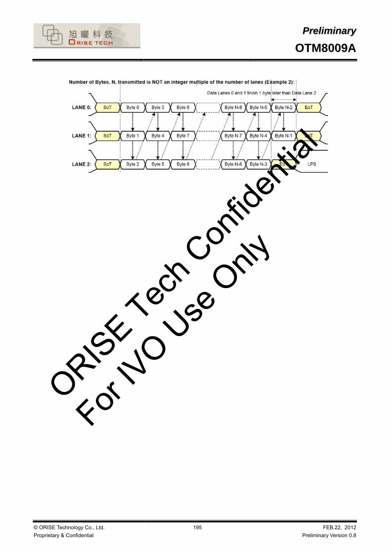
PPrreelliimmiinnaarryy
OTM8009A
© ORISE Technology Co., Ltd.
Proprietary & Confidential
195 FEB.22, 2012
Preliminary Version 0.8
ORISE Tec
h Con
fiden
tial
For IV
O Use
Only

PPrreelliimmiinnaarryy
OTM8009A
© ORISE Technology Co., Ltd.
Proprietary & Confidential
196 FEB.22, 2012
Preliminary Version 0.8
6.2.4. Packet level communication
6.2.4.1. Short Packet (SPa) and Long Packet (LPa) structures
Short Packet (SPa) and Long Packet (LPa) are always used when data transmission is done in Low Power Data Transmission (LPDT) or High-Speed Data Transmission (HSDT) modes.
The lengths of the packets are
Short Packet (SPa): 4 bytes
Long Packet (LPa): From 6 to 65,541 bytes
The type (SPa or LPa) of the packet can be recognized from their package headers (PH).
Figure 6.2.4.1.1. Short packet structure
Figure 6.2.4.1.2. Long packet structure
Note:
“Figure 6.2.4.1.1: Short Packet (SPa) Structure” and ”Figure 6.2.4.1.2: Long Packet (LPa) Structure” are presenting a single packet sending (= Includes LP-11, SoT and EoT for each packet sending).
The other possibility is that there is not needed SoT, EoT and LP-11 between packets if packets have sent in multiple packet format. e.g.:
LP-11 =>SoT =>SPa =>LPa =>SPa =>SPa =>EoT =>LP-11
LP-11 =>SoT =>SPa =>SPa =>SPa =>EoT =>LP-11
LP-11 =>SoT =>LPa =>LPa =>LPa =>EoT =>LP-11
ORISE Tec
h Con
fiden
tial
For IV
O Use
Only

PPrreelliimmiinnaarryy
OTM8009A
© ORISE Technology Co., Ltd.
Proprietary & Confidential
197 FEB.22, 2012
Preliminary Version 0.8
Bit Order of the Byte on Packets
All packet data traverses the interface as bytes. Sequentially, a transmitter shall send data LSB first, MSB last. For packets with multi-byte fields, the least significant byte shall be transmitted first unless otherwise specified.
Figure 6.2.4.1.3 shows a complete Long packet data transmission. Note, the figure shows the byte values in standard positional notation, i.e. MSB on the left and LSB on the right, while the bits are shown in chronological order with the LSB on the left, the MSB on the right and time increasing left to right.
Figure 6.2.4.1.3. Bit order of the byte on packets
Byte Order of the Multiple Byte Information on Packets
Byte order of the multiple bytes information, what is used on packets, is that the Least Significant (LS) Byte of the information is sent in the first and the Most Significant (MS) Byte of the information is sent in the last.
e.g. Word Count (WC) consists of 2 bytes (16 bits) when the LS byte is sent in the first and the MS byte is sent in the last.
This same order is illustrated for reference purposes below.
Figure 6.2.4.1.4. Byte order of the multiple byte information on packets
Packet Head (PH)
The packet header is always consisting of 4 bytes. The content of these 4 bytes are different if it is used to Short Packet (SPa) or Long Packet (LPa).
Short Packet (SPa):
1st byte: Data Identification (DI) => Identification that this is Short Packet (SPa)
2nd and 3rd bytes: Packet Data (PD), Data 0 and 1
4th byte: Error Correction Code (ECC)
Figure 6.2.4.1.5. Packet head on short packet
ORISE Tec
h Con
fiden
tial
For IV
O Use
Only

PPrreelliimmiinnaarryy
OTM8009A
© ORISE Technology Co., Ltd.
Proprietary & Confidential
198 FEB.22, 2012
Preliminary Version 0.8
Long Packet (LPa):
1st byte: Data Identification (DI) => Identification that this is Long Packet (LPa)
2nd and 3rd bytes: Word Count (WC)
4th byte: Error Correction Code (ECC)
Figure 6.2.4.1.6. Packet head on long packet
Data Identification
Data Identification (DI) is a part of Packet Header (PH) and it consists of 2 parts:
Virtual Channel (VC), 2 bits, DI[7...6]
Data Type (DT), 6 bits, DI[5…0]
The Data Identification (DI) structure is illustrated on a table below.
Table 6.2.4.1.7. Data identification structure
Data Identification (DI) is illustrated on Packet Header (PH) for reference purposes below.
Figure 6.2.4.1.8. Data identification of the packet head
ORISE Tec
h Con
fiden
tial
For IV
O Use
Only

PPrreelliimmiinnaarryy
OTM8009A
© ORISE Technology Co., Ltd.
Proprietary & Confidential
199 FEB.22, 2012
Preliminary Version 0.8
Virtual Channel (VC)
A processor may service up to four peripherals with tagged commands or blocks of data, using the Virtual Channel ID field of the header for packets targeted at different peripherals.
Virtual Channel (VC) is a part of Data Identification (DI[7…6]) structure and it is used to address where a packet is wanted to send from the MCU. Bits of the Virtual Channel (VC) are illustrated for reference purposes below.
OTM8009A only support VC code=00, package with other VC code(01/10/11) will be filter out.
Figure 6.2.4.1.9. Virtual channel on the packet head
Figure 6.2.4.1.10. Virtual channel block diagram (receiver case)
Data Type (DT)
Data Type (DT) is a part of Data Identification (DI[5…0]) structure and it is used to define a type of the used data on a packet.
Bits of the Data Type (DT) are illustrated for reference purposes below.
Figure 6.2.4.1.11. Data type on the packet head
This Data Type (DT) also defines what the used packet is: Short Packet (SPa) or Long Packet (LPa). Data Types (DT) are different from the MCU to the display module (or other devices) and vice versa. These Data Type (DT) are defined on tables below.
ORISE Tec
h Con
fiden
tial
For IV
O Use
Only

PPrreelliimmiinnaarryy
OTM8009A
© ORISE Technology Co., Ltd.
Proprietary & Confidential
200 FEB.22, 2012
Preliminary Version 0.8
Table 6.2.4.1.12. Data type from the MCU to the display module
Table 6.2.4.1.13. Data type from the display module to the MCU
The receiver is ignored other Data Type (DT) if they are not defined on tables above.
Host send “Generic Read” data type, OTM8009A will return DCS Read package to Host.
Packet data on the short packet
Packet Data (PD) of the Short Packet (SPa) is defined after Data Type (DT) of the Data Identification (DI) has indicated that Short Packet (SPa) is wanted to send.
Packet Data (PD) of the Short Packet (SPa) consists of 2 data bytes: Data 0 and Data 1.
Packet Data (PD) sending order is that Data 0 is sent in the first and the Data 1 is sent in the last.
Bits of Data 1 are set to 00h, if the information length is 1 byte.
Packet Data (PD) of the Short Packet (SPa), when the length of the information is 1 or 2 bytes are illustrated for reference purposes below.
ORISE Tec
h Con
fiden
tial
For IV
O Use
Only

PPrreelliimmiinnaarryy
OTM8009A
© ORISE Technology Co., Ltd.
Proprietary & Confidential
201 FEB.22, 2012
Preliminary Version 0.8
Figure 6.2.4.1.14. Packet data on the short packet, 2 bytes information
Packet Data (PD) information:
Data 0: 10hex
Data 1: 00hex (Null)
Figure 6.2.4.1.15. Packet data on the short packet, 1 bytes information
Word count on the long packet
Word Count (WC) of the Long Packet (LPa) is defined after Data Type (DT) of the Data Identification (DI)has indicated that Long Packet (LPa) is wanted to send.
Word Count (WC) indicates a number of the data bytes of the Packet Data (PD) what is wanted to send after Packet Header (PH) versus Packet Data (PD) of the Short Packet (SPa) is placed in the Packet Header (PH).
Word Count (WC) of the Long Packet (LPa) consists of 2 bytes.
These 2 bytes of the Word Count (WC) sending order is that the Least Significant (LS) Byte is sent in the first and the Most Significant (MS) Byte is sent in the last.
Word Count (WC) of the Long Packet (LPa) is illustrated for reference purposes below.
Figure 6.2.4.1.16. Word count on the long packet
ORISE Tec
h Con
fiden
tial
For IV
O Use
Only

PPrreelliimmiinnaarryy
OTM8009A
© ORISE Technology Co., Ltd.
Proprietary & Confidential
202 FEB.22, 2012
Preliminary Version 0.8
Error Correction Code (ECC)
Error Correction Code (ECC) is a part of Packet Header (PH) and its purpose is to identify an error or errors:
Short Packet (SPa): Data Identification (DI) and Packet Data (PD) bytes (24 bits: D[23…0])
Long Packet (LPa): Data Identification (DI) and Word Count (WC) bytes (24 bits: D[23…0])
D[23…0] is illustrated for reference purposes below.
Figure 6.2.4.1.17. D[23:0] and P[7:0] on the short packet
Figure 6.2.4.1.18. D[23:0] and P[7:0] on the long packet
Error Correction Code (ECC) can recognize one error or several errors and makes correction in one bit error case.
Bits (P[7…0]) of the Error Correction Code (ECC) are defined, where the symbol ‘^’ is presenting XOR function (Pn is ‘1’ if there is odd number of ‘1’s and Pn is ‘0’ if there is even number of ‘1’s), as follows.
P7 = 0
P6 = 0
P5 = D10^D11^D12^D13^D14^D15^D16^D17^D18^D19^D21^D22^D23
P4 = D4^D5^D6^D7^D8^D9^D16^D17^D18^D19^D20^D22^D23
P3 = D1^D2^D3^D7^D8^D9^D13^D14^D15^D19^D20^D21^D23
P2 = D0^D2^D3^D5^D6^D9^D11^D12^D15^D18^D20^D21^D22
P1 = D0^D1^D3^D4^D6^D8^D10^D12^D14^D17^D20^D21^D22^D23
P0 = D0^D1^D2^D4^D5^D7^D10^D11^D13^D16^D20^D21^D22^D23
P7 and P6 are set to ‘0’ because Error Correction Code (ECC) is based on 64 bit value ([D63…0]), but this implementation is based on 24 bit value (D[23…0]). Therefore, there is only needed 6 bits (P[5…0]) for Error Correction Code (ECC).
ORISE Tec
h Con
fiden
tial
For IV
O Use
Only

PPrreelliimmiinnaarryy
OTM8009A
© ORISE Technology Co., Ltd.
Proprietary & Confidential
203 FEB.22, 2012
Preliminary Version 0.8
Figure 6.2.4.1.19 24-bit ECC generation on TX side (Example)
ORISE Tec
h Con
fiden
tial
For IV
O Use
Only

PPrreelliimmiinnaarryy
OTM8009A
© ORISE Technology Co., Ltd.
Proprietary & Confidential
204 FEB.22, 2012
Preliminary Version 0.8
Packet footer on the long packet
Packet Footer (PF) of the Long Packet (LPa) is defined after the Packet Data (PD) of the Long Packet (LPa). The Packet Footer (PF) is a checksum value what is calculated from the Packet Data of the Long Packet (LPa).
The checksum is using a 16-bit Cyclic Redundancy Check (CRC) value which is generated with a polynomial X16+X12+X5+X0 as it is illustrated below.
Figure 6.2.4.1.20 16-bit cyclic redundancy check (CRC) calculation
The 16-bit Cyclic Redundancy Check (CRC) generator is initialized to FFFFh before calculations.
The Most Significant Bit (MSB) of the data byte of the Packet Data (PD) is the first bit what is inputted into the 16-bit Cyclic Redundancy Check (CRC).
The receiver is calculated own checksum value from received Packet Data (PD). The receiver compares own checksum and the Packet Footer (PF) what the transmitter has sent.
The received Packet Data (PD) and Packet Footer (PF) are correct if the own checksum of the receiver and Packet Footer (PF) are equal and vice versa the received Packet Data (PD) and Packet Footer (PF) are not correct if the own checksum of the receiver and Packet Footer (PF) are not equal.
ORISE Tec
h Con
fiden
tial
For IV
O Use
Only

PPrreelliimmiinnaarryy
OTM8009A
© ORISE Technology Co., Ltd.
Proprietary & Confidential
205 FEB.22, 2012
Preliminary Version 0.8
6.2.4.2. Packet transmissions
Packet from the MCU to the display module
Display Command Set (DCS), which is defined on chapter “Instructions” is used from the MCU to the display module.
This Display Command Set (DCS) is always defined on the Data 0 of the Packet Data (PD), which is included in Short Packet (SPa) and Long packet (LPa) as these are illustrated below.
Figure 6.2.4.2.1. DCS on the short packet and long packet
Packet from the display module to the MCU
Used packet types
The display module is always using Short Packet (SPa) or Long Packet (LPa), when it is returning information to the MCU after the MCU has requested information from the Display Module. This information can be a response of the Display Command Set (DCS).
The used packet type is defined on Data Type (DT). See chapter “7.5.4.1.3.1.2. Data Type (DT)”.
Figure 6.2.4.2.2. Return bytes on single packet
ORISE Tec
h Con
fiden
tial
For IV
O Use
Only

PPrreelliimmiinnaarryy
OTM8009A
© ORISE Technology Co., Ltd.
Proprietary & Confidential
206 FEB.22, 2012
Preliminary Version 0.8
Acknowledge with Error Report (AwER)
“Acknowledge with Error Report” (AwER) is always using a Short Packet (SPa), what is defined on Data Type (DT, 00 0010b), from the display module to the MCU.
The Packet Data (PD) can include bits, which are defining the current error, when a corresponding bit is set to 1 , as they are defined on the following table.
Figure 6.2.4.2.3. Acknowledge with error report for long packet response
Figure 6.2.4.2.4. Acknowledge with error report for short packet response
These errors are only included on the last packet, which has been received from the MCU to the display module, before Bus Turnaround (BTA).
The display module ignores the received packet which includes error or errors.
Acknowledge with Error Report (AwER) of the Short Packet (SPa) is defined e.g.
Data Identification (DI)
o Virtual Channel (VC, DI[7…6]): 00b
o Data Type (DT, DI[5…0]): 00 0010b
Packet Data (PD)
o Bit 8: ECC Error, single-bit (detected and corrected)
o AwER: 0100h
Error Correction Code (ECC)
This is defined on the Short Packet (SPa) as follows.
ORISE Tec
h Con
fiden
tial
For IV
O Use
Only

PPrreelliimmiinnaarryy
OTM8009A
© ORISE Technology Co., Ltd.
Proprietary & Confidential
207 FEB.22, 2012
Preliminary Version 0.8
Figure 6.2.4.2.5. Acknowledge with error report – example
6.2.5. Customer-defined generic read data type format
The short packet of Data Type 24h (Generic READ, 2 parameters) specifies the register content for read and the Nth parameter that will begin reading. After Data Type 24h is received, BTA is executed. Then, the Nth parameter becomes the first data, and the number of data of WC (word count) value is output.
Figure 6.2.5.1. Generic read data type format
ORISE Tec
h Con
fiden
tial
For IV
O Use
Only

PPrreelliimmiinnaarryy
OTM8009A
© ORISE Technology Co., Ltd.
Proprietary & Confidential
208 FEB.22, 2012
Preliminary Version 0.8
6.3. MDDI Interface
6.3.1. General description
The MDDI is a differential and serial interface with high speed. The OTM8009A support the MDDI Type 1 and Type 2.
MDDI
Host
MDDI
Client
Forward
Reverse
Data1+
Data1-
Data1+
Data1-
Data0+
Data0-
Data0+
Data0-
STB+
STB-
STB+
STB-
ORISE Tec
h Con
fiden
tial
For IV
O Use
Only

PPrreelliimmiinnaarryy
OTM8009A
© ORISE Technology Co., Ltd.
Proprietary & Confidential
209 FEB.22, 2012
Preliminary Version 0.8
6.3.2. MDDI Packet summary
The OTM8009A support packet type as shown in table.
Table 6.3.2.1 The support packet type
Packet Name Packet Type
(Dec) Direction
Sub-frame header packet 15359 Forward
Filler packet 0 Forward
Reverse link encapsulation packet 65 Forward
Link shutdown packet 69 Forward
Link Control Packets
Round-trip delay measurement packet 82 Forward
Basic Media Stream Packets
Video stream packet 16 Forward
Client capability packet 66 Reverse
Client request and status packet 70 Reverse Client Status and Control Packets
Register access packet 146 Forward / Reverse
6.3.3. MDDI Packet format
The structure of the forward link is illustrated in Figure 6.2.3.1. Information transmitted over the MDDI link is grouped into packets. The definition of the types of packets is given later in this section. Multiple packets are grouped together into a sub-frame, and multiple sub-frames make up a media- frame. Every sub-frame begins with a special packet called a Sub-frame Header Packet.
Table 6.3.3.1 Forward link structure
ORISE Tec
h Con
fiden
tial
For IV
O Use
Only

PPrreelliimmiinnaarryy
OTM8009A
© ORISE Technology Co., Ltd.
Proprietary & Confidential
210 FEB.22, 2012
Preliminary Version 0.8
6.3.3.1. Sub frame header packet
The Sub-Frame Header Packet is the first packet of every sub-frame, and its basic structure is illustrated in Figure 6.2..3.1.1. The Sub-Frame Header Packet is required for host-client synchronization. Every host shall be able to generate this packet, and every client shall be able to receive and interpret this packet.
Figure 6.3.3.1.1 Sub frame header packet format
Packet Contents:
Packet Length – 2 bytes that contain a 16-bit unsigned integer that specifies the total number of bytes in the packet not including the packet length field. The Packet Length of this packet is always 20.
Packet Type – 2 bytes that contain a 16-bit unsigned integer. A Packet Type of 15359 (0x3bff hexadecimal) identifies the packet as a Sub-frame Header Packet.
Unique Word – 2 bytes that contain a 16-bit unsigned integer that contains the 16 most significant bits of the unique word. The 4-byte combination of the Packet Type and Unique Word together form a 32-bit unique word with good autocorrelation. The actual unique word is 0x005a3bff where the lower 16 bits are transmitted first as the Packet Type, and the most significant 16 bits are transmitted immediately afterward.
Reserved 1 – 2 bytes that contain a 16-bit unsigned integer that is reserved for future use. All bits in this field shall be set to zero. The purpose of this field is to cause all subsequent 2 byte fields to align to a 16-bit word address and cause 4-byte fields to align to a 32-bit word address. The least significant byte is reserved to indicate that the host is capable of addressing multiple client devices. A value of zero is reserved to indicate that the host is capable of operating only with a single client device.
Sub-frame Length – 4 bytes that contain a 32-bit unsigned integer that specifies the number of bytes per sub-frame. It is valid to change the Sub-frame Length on-the-fly from one sub-frame to the next. This is useful in order to make minor timing adjustments in the sync-pulses for isochronous streams. If the CRC of the Sub-frame Header packet is not valid then the link controller shall use the Sub-frame Length of the previous known-good Sub-frame Header packet to estimate the length of the current sub-frame.
Protocol Version – 2 bytes that contain a 16-bit unsigned integer that specifies the protocol version used by the host. The Protocol Version field shall be set to 0 to specify the version of the protocol described in this document.
Sub-frame Count – 2 bytes that contain a 16-bit unsigned integer that specifies a sequence number that indicates the number of sub-frames that have been transmitted since the beginning of the media-frame. The first sub-frame of the media-frame has a Sub-frame Count of zero. The last sub-frame of the media-frame has a value of n-1, where n is the number of sub-frames per media-frame. The value in the Sub-frame Count field shall be equal to the Sub-frame Count sent in the previous Sub-frame Header Packet plus 1, except for the first sub-frame of a media-frame when the Sub-frame Count shall be zero.
Media-frame Count – 4 bytes that contain a 32-bit unsigned integer that specifies a sequence number that indicates the number of media-frames that have been transmitted since the beginning of the present media item. The first media-frame of the media item has a Media- frame Count of zero. The Media-frame Count increments immediately prior to the first sub- frame of each media-frame and wraps back to zero after the maximum Media-frame Count (media-frame number 232-1 = 4,294,967,295) is used. The Media-frame Count value may be reset at any time by the host to suit the needs of the end application.
CRC – 2 bytes that contain a 16-bit CRC of all bytes in the packet including the Packet Length.
ORISE Tec
h Con
fiden
tial
For IV
O Use
Only

PPrreelliimmiinnaarryy
OTM8009A
© ORISE Technology Co., Ltd.
Proprietary & Confidential
211 FEB.22, 2012
Preliminary Version 0.8
6.3.3.2. Video stream packet
The Video Stream Packets carry video data to update a rectangular region of the display. The size of this region may be as small as a single pixel or as large as the entire display. There may be an unlimited number of streams displayed simultaneously (limited only by system resources) because all context required to display a stream is contained within the Video Stream Packet. The format of the Video Stream Packet is illustrated in Figure 6.2.3.2.1. The client shall indicate its capability to receive a Video Stream Packet via the RGB Capability, Monochrome Capability, and Y Cr Cb Capability fields of the Client Capability Packet.
Figure 6.3.3.2.1 Video stream packet
Packet Contents:
Packet Length – 2 bytes that contain a 16-bit unsigned integer that specifies the total number of bytes in the packet not including the packet length field.
Packet Type – 2 bytes that contain a 16-bit unsigned integer. A Packet Type of ‘0010h’ identifies the packet as a Video Stream Packet.
bClient ID – 2 bytes that contain a 16-bit unsigned integer reserved for the Client ID. This field is reserved for future use and shall be set to ‘0000h’.
Video Data Format Descriptor – 2 bytes that contain a 16-bit unsigned integer that specifies the format of each pixel in the Pixel Data in the present stream in the present packet.
bits[15:13] = 010 : Value fixed.
bits[12] = 1 : Only packed type is available (fixed value)
bits[11:0] = 010101100101 (565h) : 16bpp (RGB(565))
= 011001100110 (666h) : 18bpp (RGB(666)
= 100010001000 (888h) : 24bpp (RGB(888))
MDDI Data Type D7 D6 D5 D4 D3 D2 D1 D0 Color
Byte n G2 G1 G0 B4 B3 B2 B1 B0RGB 5:6:5 Byte n+1 R4 R3 R2 R1 R0 G5 G4 G3
65K-Color
Byte n G1 G0 B5 B4 B3 B2 B1 B0
Byte n+1 R3 R2 R1 R0 G5 G4 G3 G2RGB 6:6:6
Byte n+2 B5 B4 B3 B2 B1 B0 R5 R4
262K-Color
Byte n B7 B6 B5 B4 B3 B2 B1 B0
Byte n+1 G7 G6 G5 G4 G3 G2 G1 G0RGB 8:8:8
Byte n+2 R7 R6 R5 R4 R3 R2 R1 R0
16.7M-Color
Figure 6.3.3.2.2 Packed pixel data format
Pixel Data Attributes – 2 bytes that contain a 16-bit unsigned integer.
o Bits [1:0] – Select the display where the pixel data must be routed. Set 2’b11 for pixel data is displayed to both eyes. Other value (2’b00, 2’b01, 2’b10) is not support.
o Bits [15:2] – Not support. Please set to 14’d0
X Left Edge – 2 bytes that contain a 16-bit unsigned integer that specifies the X coordinate of the left edge of the screen window filled by the Pixel Data field. Please refer to “Example of Video Stream Packet Fields”
Y Top Edge – 2 bytes that contain a 16-bit unsigned integer that specifies the Y coordinate of the top edge of the screen window filled by the Pixel Data field. Please refer to “Example of Video Stream Packet Fields”
ORISE Tec
h Con
fiden
tial
For IV
O Use
Only

PPrreelliimmiinnaarryy
OTM8009A
© ORISE Technology Co., Ltd.
Proprietary & Confidential
212 FEB.22, 2012
Preliminary Version 0.8
X Right Edge – 2 bytes that contain a 16-bit unsigned integer that specifies the X coordinate of the right edge of the window being updated. Please refer to “Example of Video Stream Packet Fields”
Y Bottom Edge – 2 bytes that contain a 16-bit unsigned integer that specifies the Y coordinate of the bottom edge of the window being updated. Please refer to “Example of Video Stream Packet Fields”
X Start – 2 bytes that contain a 16-bit unsigned integer that specifies the absolute X coordinate, where the point (X Start, Y Start) is the first pixel in the Pixel Data field below. Please refer to “Example of Video Stream Packet Fields”
Y Start – 2 bytes that contain a 16-bit unsigned integer that specifies the absolute Y coordinate, where the point (X Start, Y Start) is the first pixel in the Pixel Data field below. Please refer to “Example of Video Stream Packet Fields”
Pixel Count – 2 bytes that contain a 16-bit unsigned integer that specifies the number of pixels in the Pixel Data field below.
Parameter CRC – 2 bytes that contain a 16-bit CRC of all bytes from the Packet Length to the Pixel Count. If this CRC fails to check then the entire packet shall be discarded.
Pixel Data – The raw video information to be displayed. Data is formatted in the manner described by the Video Data Format Descriptor field. If bit 5 of the Pixel Data Attributes field is set to one then the Pixel Data field contains exactly one row of pixels, where the first pixel transmitted corresponds to the leftmost pixel and the last pixel transmitted corresponds to the right-most pixel.
Pixel Data CRC – 2 bytes that contain a 16-bit CRC of only the Pixel Data. If this CRC fails to check then the Pixel Data may still be used but the CRC error count shall be incremented.
Example of Video Stream Packet Fields
ORISE Tec
h Con
fiden
tial
For IV
O Use
Only
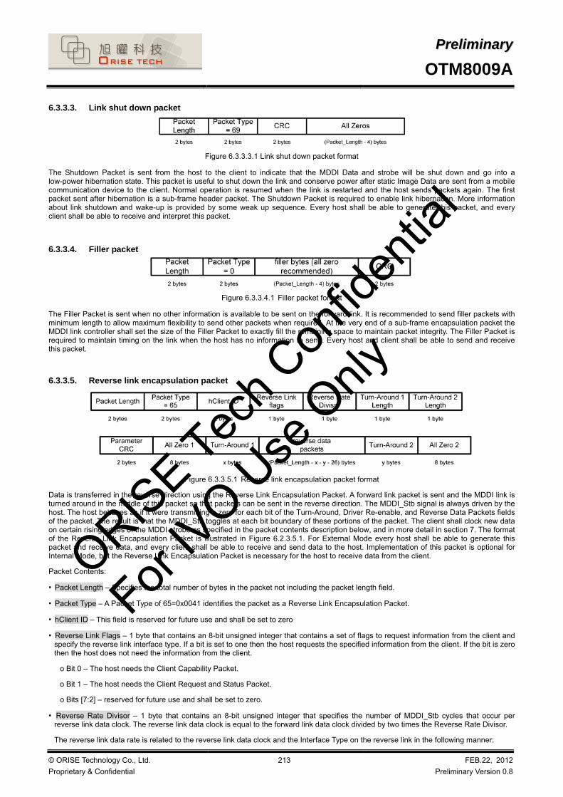
PPrreelliimmiinnaarryy
OTM8009A
© ORISE Technology Co., Ltd.
Proprietary & Confidential
213 FEB.22, 2012
Preliminary Version 0.8
6.3.3.3. Link shut down packet
Figure 6.3.3.3.1 Link shut down packet format
The Shutdown Packet is sent from the host to the client to indicate that the MDDI Data and strobe will be shut down and go into a low-power hibernation state. This packet is useful to shut down the link and conserve power after static Image Data are sent from a mobile communication device to the client. Normal operation is resumed when the link is restarted and the host sends packets again. The first packet sent after hibernation is a sub-frame header packet. The Shutdown Packet is required to enable link hibernation. More information about link shutdown and wake-up is provided by some weak up sequence. Every host shall be able to generate this packet, and every client shall be able to receive and interpret this packet.
6.3.3.4. Filler packet
Figure 6.3.3.4.1 Filler packet format
The Filler Packet is sent when no other information is available to be sent on the forward link. It is recommended to send filler packets with minimum length to allow maximum flexibility to send other packets when required. At the very end of a sub-frame encapsulation packet the MDDI link controller shall set the size of the Filler Packet to exactly fill the remaining space to maintain packet integrity. The Filler Packet is required to maintain timing on the link when the host has no information to send. Every host and client shall be able to send and receive this packet.
6.3.3.5. Reverse link encapsulation packet
Figure 6.3.3.5.1 Reverse link encapsulation packet format
Data is transferred in the reverse direction using the Reverse Link Encapsulation Packet. A forward link packet is sent and the MDDI link is turned around in the middle of this packet so that packets can be sent in the reverse direction. The MDDI_Stb signal is always driven by the host. The host behaves as if it were transmitting a zero for each bit of the Turn-Around, Driver Re-enable, and Reverse Data Packets fields of the packet. The result is that the MDDI_Stb toggles at each bit boundary of these portions of the packet. The client shall clock new data on certain rising edges of the MDDI strobe as specified in the packet contents description below, and in more detail in section 7. The format of the Reverse Link Encapsulation Packet is illustrated in Figure 6.2.3.5.1. For External Mode every host shall be able to generate this packet and receive data, and every client shall be able to receive and send data to the host. Implementation of this packet is optional for Internal Mode, but the Reverse Link Encapsulation Packet is necessary for the host to receive data from the client.
Packet Contents:
• Packet Length – Specifies the total number of bytes in the packet not including the packet length field.
• Packet Type – A Packet Type of 65=0x0041 identifies the packet as a Reverse Link Encapsulation Packet.
• hClient ID – This field is reserved for future use and shall be set to zero
• Reverse Link Flags – 1 byte that contains an 8-bit unsigned integer that contains a set of flags to request information from the client and specify the reverse link interface type. If a bit is set to one then the host requests the specified information from the client. If the bit is zero then the host does not need the information from the client.
o Bit 0 – The host needs the Client Capability Packet.
o Bit 1 – The host needs the Client Request and Status Packet.
o Bits [7:2] – reserved for future use and shall be set to zero.
• Reverse Rate Divisor – 1 byte that contains an 8-bit unsigned integer that specifies the number of MDDI_Stb cycles that occur per reverse link data clock. The reverse link data clock is equal to the forward link data clock divided by two times the Reverse Rate Divisor.
The reverse link data rate is related to the reverse link data clock and the Interface Type on the reverse link in the following manner:
ORISE Tec
h Con
fiden
tial
For IV
O Use
Only

PPrreelliimmiinnaarryy
OTM8009A
© ORISE Technology Co., Ltd.
Proprietary & Confidential
214 FEB.22, 2012
Preliminary Version 0.8
o Interface Type 1 – reverse data rate = reverse link data clock.
o Interface Type 2 – reverse data rate = two times reverse link data clock.
o Interface Type 3 – reverse data rate = four times reverse link data clock.
o Interface Type 4 – reverse data rate = eight times reverse link data clock.
• Turn-Around 1 Length – Specifies the total number of bytes that are allocated for Turn-Around 1.
• Turn-Around 2 Length – Specifies the total number of bytes that are allocated for Turn-Around 2.
• Parameter CRC – Contain a 16-bit CRC of all bytes from the Packet Length to the Turn-Around Length. If this CRC fails to check then the entire packet shall be discarded
• All Zero 1 – 8 bytes that each contain an 8-bit unsigned integer equal to zero. This field ensures that all MDDI_Data signals are at a logic-zero level for a sufficient time to allow the client to begin recovering clock using only MDDI_Stb prior to disabling the host’s line drivers during the Turn-Around 1 field.
• Turn-Around 1 – First turn-around period. The number of bytes specified by the Turn-Around 1 Length parameter is allocated to allow the MDDI_Data line drivers in the client to enable before the line drivers in the host are disabled. The client shall enable its MDDI_Data line drivers during bit 0 of Turn-Around 1 and the host shall disable its outputs and be completely disabled prior to the last bit of Turn-Around 1. The MDDI_Stb signal behaves as though MDDI_Data0 were at a logic-zero level during the entire Turn-Around 1 period.
• Reverse Data Packets – A series of data packets transferred from the client to host. The client may send filler packets or drive the MDDI_Data lines to a logic-zero level when it has no data to send to the host. If the MDDI_Data lines are driven to zero the host will interpret this as a packet with a zero length (not a valid length) and the host will accept no additional packets from the client for the duration of the current Reverse Link Encapsulation Packet.
• Turn-Around 2 – The second turn-around period. The number of bytes is specified by the Turn-Around Length parameter. The host shall wait for at least the round trip delay time before it enables its MDDI_Data line drivers during Turn-Around 2. The host shall enable its MDDI_Data line drivers and be completely enabled prior to the last bit of Turn-Around 2 and the client shall disable its outputs and be completely disabled prior to the last bit of Turn-Around 2. The purpose of Turn-Around 2 is to allow the remaining amount of data from the Reverse Data Packets field to be transmitted from the client. Due to variations in different systems and the amount of safety margin allocated it is possible that neither the host nor client will be driving the MDDI_Data signals to a logic-zero level during some parts of the Turn-Around 2 field as seen by the line receivers at the host. The MDDI_Stb signal behaves as though MDDI_Data0 were at a logic-zero level during the entire Turn-Around 2 period.
• All Zero 2 – 8 bytes that each contains an 8-bit unsigned integer equal to zero. This field ensures that all MDDI_Data signals are at a logic-zero level for a sufficient time to allow the client to begin recovering clock using both MDDI_Data0 and MDDI_Stb after enabling the host’s line drivers following the Turn-Around 2 field.
6.3.3.6. Round-trip delay measurement packet
Figure 6.3.3.6.1 Round-trip delay measurement packet format
The Round-Trip Delay Measurement Packet is used to measure the propagation delay from the host to the client plus the delay from the client back to the host. This measurement inherently includes all of the delays that exist in the line drivers and receivers and the interconnect subsystem. This measurement is used to set the turn around delay and reverse link rate divisor parameters in the Reverse Link Encapsulation Packet. This packet is most useful when the MDDI link is running at the maximum speed intended for a particular application. The packet may be sent in Type I mode and at a lower data rate to increase the range of the Round-Trip delay measurement.
Packet Contents:
• Packet Length – Specifies the total number of bytes in the packet not including the packet length field. The Packet Length is always 200.
• Packet Type – A Packet Type of 82=0x0052 identifies the packet as a Round-Trip Delay Measurement Packet.
• hClient ID – This field is reserved for future use and shall be set to zero.
• Parameter CRC – Contain a 16-bit CRC of all bytes from the Packet Length to the Packet Type. If this CRC fails to check then the entire packet shall be discarded.
• Guard Time 1 – 64 bytes to allow the MDDI_Data line drivers in the client to enable before the line drivers in the host are disabled. The client shall enable its MDDI_Data line drivers during bit 0 of Guard Time 1 and the host shall disable its line drivers and be completely disabled prior to the last bit of Guard Time 1. The host and client shall both drive a logic zero level during Guard Time 1 when they are not
ORISE Tec
h Con
fiden
tial
For IV
O Use
Only

PPrreelliimmiinnaarryy
OTM8009A
© ORISE Technology Co., Ltd.
Proprietary & Confidential
215 FEB.22, 2012
Preliminary Version 0.8
disabled. Another purpose of this field is to ensure that all MDDI_Data signals are at a logic-zero level for a sufficient time to allow the client to begin recovering clock using only MDDI_Stb prior to disabling the host’s line drivers.
• Measurement Period – a 64 byte window to allow the client to respond with two bytes of 0xff and 30 bytes of 0x00 at half the data rate used on the forward link. This rate corresponds to a Reverse Link Rate Divisor of 1. The client returns this response immediately at the time it perceives as the beginning of the Measurement Period. This response from the client will be received at the host at precisely the round trip delay of the link plus logic delay in the client after the beginning of the first bit of the Measurement Period at the host.
• All Zero – 2 bytes that each contains an 8-bit unsigned integer equal to zero. This field allows the MDDI_Data line drivers in the host and client to overlap so that MDDI_Data is always driven. The host shall enable its MDDI_Data line drivers during bit 0 of the All Zero field, and the client shall also continue to drive the signal to a logic-zero level as it did at the end of the Measurement Period.
Figure 6.3.3.6.2 Round-trip delay measurement timing
Figure 6.2.3.6.2 illustrates the timing of events during the Round-Trip Delay Measurement Packet. The host transmits the Round-Trip Delay Measurement Packet and a delay is incurred before the packet reaches the client. As the client receives the packet it transmits the 0xff, 0xff, and 30 bytes of 0x00 pattern precisely at the beginning of the Measurement Period as detected by the client. The actual time the client begins to transmit this sequence is delayed from the beginning of the Measurement Period when viewed at the host. The amount of this delay is precisely the time it takes for the packet to propagate down the cable, through the line receivers and drivers in the client, and back through the cable to the host.
The host shall count the number of forward-link bit times from the start of the Measurement Period to the beginning of the 0xff, 0xff, and 30 bytes of 0x00 sequence. When a Type 2 – 4 reverse link is being used the host shall measure and save the round-trip delay value of all MDDI_Data pairs in case the data rate and round-trip delay skew are large enough to affect the arrival time if each bit differently.
The host and client both drive the line to a logic-zero level during both guard times to keep the MDDI_Data lines in a defined state. The enable and disable times of the host and client during both guard times are such that the MDDI_Data signals are always at a valid low for any valid round-trip delay time.
6.3.3.7. Register access packet
Figure 6.3.3.7.1 Register access packet format
The Register Access Packet provides either the host or client with a means to access configuration and status registers in the opposite end of the MDDI link. The registers are likely to be unique for each display or device controller. These registers already exist in many displays that require setting configurations, modes of operation, and other useful and necessary settings. The Register Access Packet allows the MDDI host or client to both write to a register and request to read a register via the MDDI link. When the host or client requests to read a register, the opposite end shall respond by sending the register data in the same packet type but indicating that this is the data read from a particular register with the use of the Read/Write Info field. The Register Access Packet may be used to read or write multiple registers by specifying a register count greater than 1.The client shall indicate its ability to support the Register Access Packet via bit 22 of Client Feature Capability Indicators field of the Client Capability Packet.
Packet Contents:
• Packet Length – Specifies the total number of bytes in the packet not including the packet length field.
• Packet Type – A Packet Type of 146=0x0092 identifies the packet as a Register Access Packet.
• bClient ID – This field is reserved for future use and shall be set to zero.
• Read/Write Info – Specifies the packet as either a write, or a read, or a response to a read, and provides a count of the data values.
o Bits [15:14] – Read/Write Flags
o Bits [13:0] – a 14-bit unsigned integer that specifies the number of 32-bit Register Data List items to be transferred in the Register Data List field.
ORISE Tec
h Con
fiden
tial
For IV
O Use
Only

PPrreelliimmiinnaarryy
OTM8009A
© ORISE Technology Co., Ltd.
Proprietary & Confidential
216 FEB.22, 2012
Preliminary Version 0.8
o If bits [15:14] equal 00 then bits [13:0] specify the number of 32-bit register data items that are contained in the Register Data List field to be written to registers starting at the register specified by the Register Address field.
o If bits [15:14] equal 10 then bits [13:0] specify the number of 32-bit register data items that the receiving device shall send to the device requesting that the registers be read. The Register Data List field in this packet shall contain no items and is of zero length.
o If bits [15:14] equal 11 then bits [13:0] specify the number of 32-bit register data items that have been read from registers that are contained in the Register Data List field.
o Bits [15:14] shall not be equal to 01. This is not a valid value and is reserved for future use.
• Register Address – Contains the register address that is to be written to or read from. For addressing registers whose addressing is less than 32 bits, the upper bits shall be set to zero.
• Parameter CRC – 2 bytes that contain a 16-bit CRC of all bytes from the Packet Length to the Register Address. If this CRC fails to check then the entire packet shall be discarded.
• Register Data List – a list of 4-byte register data values to be written to client registers or values that were read from client device registers.
• Register Data CRC – 2 bytes that contain a 16-bit CRC of only the Register Data List. If this CRC fails to check then the Register Data may still be used but the CRC error count shall be incremented.
6.3.3.8. Client request and status packet
Figure 6.3.3.8.1 Client request and status packet format
The host needs a small amount of information from the client so it can configure the host-to-client link in an optimum manner. It is recommended that the client send one Client Request and Status Packet to the host each sub-frame. It is recommended that the client send this packet as the first packet in the Reverse Link Encapsulation Packet to ensure that it is delivered reliably to the host, and it is required when requested by the host via the Reverse Link Flags in the Reverse Link Encapsulation Packet. The Client Request and Status Packet is required to report errors and status to the host. For external mode every host shall be able to receive this packet, and every client shall be able to send this packet. It is highly recommended that internal mode hosts and clients also support this packet, but it is not required.
Packet Contents:
• Packet Length – Specifies the total number of bytes in the packet not including the packet length field. The Packet Length is always 12.
• Packet Type – A Packet Type of 70=0x0046 identifies the packet as a Client Request and Status Packet.
• cClient ID – This field is reserved for future use and shall be set to zero.
• Reverse Link Request – Specifies the number of bytes the client needs in the reverse link in the next sub-frame to send information to the host.
• CRC Error Count – Indicates the number of CRC errors that have occurred since the last Client Request and Status Packet was sent by the client. The CRC count is reset each time a Client Request and Status Packet is sent. If the actual number of CRC errors exceeds 255 then this value saturates at 255.
• Client Status – Contains a group of flags that indicate the current status of the client device.
o Bit 0 – Indicates that there has been a change in the capability of the client. This could be due to the user connecting a peripheral device such as a microphone, keyboard, or display, or some other reason.
Bit 0 = 1 – capability has changed. Examine the Client Capability Packet to determine the new client characteristics.
Bit 0 = 0 – capability has not changed since the last Client Capability Packet was sent.
o Bit 1 – Indicates that the client device has detected an error in processing a packet since the last Client Capability Packet was sent. Implementation of this bit is optional in the client device. Additional information about the error may be provided via other means, such as the Client Error Report Packet or via a Register Access Packet.
o Bits [7:2] – reserved for future use and shall be set to zero.
• Client Busy Flags – Indicate that the client is performing a specific function and is not ready to accept another packet related to that function. A bit set to one indicates that the particular function is currently being performed by the client and that the related function in the client is busy. If the related function in the client is ready the bit shall be zero. The client shall always return a busy status (bit set to one) for all functions that are not supported in the client.
o Bit 0 – bitmap block transfer function is busy.
o Bit 1 – bitmap area fill function is busy.
ORISE Tec
h Con
fiden
tial
For IV
O Use
Only

PPrreelliimmiinnaarryy
OTM8009A
© ORISE Technology Co., Ltd.
Proprietary & Confidential
217 FEB.22, 2012
Preliminary Version 0.8
o Bit 2 – bitmap pattern fill function is busy.
o Bit 3 – the graphics subsystem is busy performing an operation that requires use of the frame buffer in the client. Other graphics functions that require use of the frame buffer may not begin until this bit is set to one.
o Bits [15:4] – reserved for future use and shall be set to one to indicate busy status in case these bits are assigned in a future version of this standard.
• CRC – 2 bytes that contain a 16-bit CRC of all bytes in the packet including the Packet Length.
6.3.3.9. Client capability packet
Figure 6.3.3.9.1 Client capability packet format
The host needs to know the capability of the client so it can configure the host-to-client link in an optimum manner. It is recommended that the client send a Client Capability Packet to the host after forward link synchronization is acquired, and it is required when requested by the host via the Reverse Link Flags in the Reverse Link Encapsulation Packet. The Client Capability Packet is required to inform the host of the capabilities of the client. For External Mode every host shall be able to receive this packet, and every client shall be able to send this packet. Implementation of this packet is optional for Internal Mode.
Packet Contents:
• Packet Length – Specifies the total number of bytes in the packet not including the packet length field.
• Packet Type – A Packet Type of 66=0x0042 identifies the packet as a Client Capability Packet.
• cClient ID –This field is reserved for future use and shall be set to zero.
• Protocol Version – Specifies the protocol version used by the client. The present protocol version shall be set to 2.
• Minimum Protocol Version – Specifies the minimum protocol version that the client can interpret. Zero is an invalid value.
• Pre-Calibration Data Rate Capability – Specifies the maximum data rate the client can receive on each data pair on the forward MDDI link prior to performing forward link skew calibration. The rate is specified as the number of million bits per second (Mbps).
• Interface Type Capability – Specifies the interface types that are supported on the forward and reverse links. A bit set to 1 indicates that the specified interface type is supported, and a bit set to 0 indicates that the specified type is not supported. All hosts and clients shall support at least Type 1 on the forward and reverse link. It is not required to support a contiguous range of interface types. For example, it is valid to support only Type 1 and Type 3, and not Type 2 and Type 4. The forward and reverse links are not required to operate with the same interface type except when the link comes out of hibernation where both forward and reverse shall operate in Type 1 mode.
o Bit 0 – Client can function in Type 2 (2-bit) mode on the forward link.
o Bit 1 – Client can function in Type 3 (4-bit) mode on the forward link.
o Bit 2 – Client can function in Type 4 (8-bit) mode on the forward link.
ORISE Tec
h Con
fiden
tial
For IV
O Use
Only

PPrreelliimmiinnaarryy
OTM8009A
© ORISE Technology Co., Ltd.
Proprietary & Confidential
218 FEB.22, 2012
Preliminary Version 0.8
o Bit 3 – Client can function in Type 2 (2-bit) mode on the reverse link.
o Bit 4 – Client can function in Type 3 (4-bit) mode on the reverse link.
o Bit 5 – Client can function in Type 4 (8-bit) mode on the reverse link.
o Bits [7:6] are reserved and shall be set to zero.
• Number of Alt Displays – Specifies the number of alternate displays supported by the MDDI client. This value is zero in OTM8009A.
• Post-Calibration Data Rate Capability – Specifies the maximum data rate the client can receive on each data pair on the forward MDDI link after performing forward link skew calibration. The rate is specified as the number of million bits per second (Mbps). If the client device does not support the Forward Link Skew Calibration Packet then this field shall be set to zero.
• Bitmap Width – Specifies the width of the bitmap expressed as a number of pixels.
• Bitmap Height – Specifies the height of the bitmap expressed as a number of pixels.
• Display Window Width – Specifies the width of the display window expressed as a number of pixels. Often this will have the same value as the Bitmap Width.
• Display Window Height – Specifies the height of the display window expressed as a number of pixels. Often this will have the same value as the Bitmap Height.
• Color Map Size – Specifies the maximum number of table items that exist in the color map table in the client. OTM8009A cannot use the color map format then this value is zero.
• Color Map RGB Width – Specifies the number of bits of the red, green, and blue color components that can be displayed in the color map (palette) display mode. OTM8009A cannot use the color map (palette) format then this value is zero.
• RGB Capability – Specifies the number of bits of resolution that can be displayed in RGB format. If the client cannot use the RGB format then this value is zero. The RGB Capability word is composed of three separate unsigned values:
o Bits [3:0] define the maximum number of bits of blue (the blue intensity) in each pixel.
o Bits [7:4] define the maximum number of bits of green (the green intensity) in each pixel.
o Bits [11:8] define the maximum number of bits of red (the red intensity) in each pixel.
o Bits [13:12] are reserved for future use and shall be set to zero.
o Bit 14 is equal to zero this indicates that the client cannot accept RGB pixel data in unpacked format.
o Bit 15 when set to one indicates that the client can accept RGB pixel data in packed format. If bit 15 is equal to zero this indicates that the client cannot accept RGB pixel data in packed format.
• Monochrome Capability –Specifies the parameter of monochrome format. OTM8009A cannot use this format then the value is zero.
• Reserved 1 – 1 byte that contains an 8-bit unsigned integer that is reserved for future use. All bits in this field shall be set to zero.
• Y Cb Cr Capability – Specifies the parameter of Y Cb Cr format. OTM8009A cannot use the Y Cb Cr format then this value is zero.
• Bayer Capability – Specifies the parameter of Bayer format. OTM8009A cannot use the Bayer format then this value is zero.
• Reserved 2 – 2 bytes that contain a 16-bit unsigned integer that is reserved for future use. All bits in this field shall be set to zero.
• Client Feature Capability Indicators – Contains a set of flags that indicate the whether specific features in the client are supported.
A bit set to one indicates the capability is supported, and a bit set to zero indicates the capability is not supported.
o Bit 0 – the Bitmap Block Transfer Packet (packet type 71) is supported
o Bit 1 – the Bitmap Area Fill Packet (packet type 72) is supported.
o Bit 2 – the Bitmap Pattern Fill Packet (packet type 73) is supported.
o Bit 3 – the Read Frame Buffer Packet (packet type 74) is supported.
o Bit 4 – the client has the capability to support the Transparent Color and Mask Setup Packet.
o Bit 5 – the client can accept audio data in unpacked format.
o Bit 6 – the client can accept audio data in packed format.
o Bit 7 – the client can send a reverse-link video stream from a camera.
o Bit 8 – the client has the ability to receive a full line of pixel data.
o Bit 9 – the client has the ability to respond to the Display Power State Packet.
o Bit 10 – the client has the ability to support display power state 01.
ORISE Tec
h Con
fiden
tial
For IV
O Use
Only

PPrreelliimmiinnaarryy
OTM8009A
© ORISE Technology Co., Ltd.
Proprietary & Confidential
219 FEB.22, 2012
Preliminary Version 0.8
o Bit 11 – the client is communicating with a pointing device and can send and receive Pointing Device Data Packets.
o Bit 12 – the client is communicating with a keyboard and can send and receive Keyboard Data Packets.
o Bit 13 – the client has the ability to set one or more audio or video parameters by supporting the VCP Feature packets.
o Bit 14 – the client has the ability to write pixel data into the offline display frame buffer.
o Bit 15 – the client has the ability to write pixel data into only the display frame buffer currently being used to refresh the display image.
o Bit 16 – the client has the ability to write pixel data from a single Video Stream Packet into all display frame buffers.
o Bit 17 – the client has the ability to respond to the Request Specific Status Packet.
o Bit 18 – the client has the ability to respond to the Round-Trip Delay Measurement Packet.
o Bit 19 – the client has the ability to respond to the Forward Link Skew Calibration Packet.
o Bit 20 – the client has the ability to interpret the Request Specific Status Packet and respond with the Valid Status Reply List Packet.
o Bit 21 – the client has the ability to use the Raster Operation field of the Bitmap Block Transfer Packet (packet type 71).
o Bit 22 – the client has the ability to respond to the Register Access Packet
o Bits [31:23] – reserved for future use, shall be set to zero.
• Maximum Video Frame Rate Capability – Specifies the maximum video frame update capability of the client in frames per second. The
host may choose to update the image at a rate less than or equal to the value specified in this field.
• Minimum Video Frame Rate Capability – Specifies the minimum video frame update capability of the client in frames per second.
• Minimum Sub-frame Rate – Specifies the minimum sub-frame rate in frames per second.
• Audio Buffer Depth – OTM8009A can not support Audio function then this value is zero.
• Audio Channel Capability – OTM8009A can not support Audio function then this value is zero.
• Audio Sample Rate Capability (forward link) – OTM8009A can not support Audio function then this value is zero.
• Audio Sample Resolution (forward link) – OTM8009A can not support Audio function then this value is zero.
• Mic Audio Sample Resolution (reverse link) – OTM8009A can not support Audio function then this value is zero.
• Mic Sample Rate Capability (reverse link) – OTM8009A can not support Audio function then this value is zero.
• Keyboard Data Format – OTM8009A can not support Audio function then this value is zero.
• Pointing Device Data Format – OTM8009A can not support Audio function then this value is zero.
• Content Protection Type – OTM8009A can not support Audio function then this value is zero.
• Mfr Name – 2 bytes that form a 16-bit value that contains the EISA 3-character ID of the manufacturer, packed into three 5-bit characters in the same manner as in the VESA EDID specification. The character ‘A’ is represented as 00001 binary, the character ‘Z’ is represented as 11010 binary, and all letters between ‘A’ and ‘Z’ are represented as sequential binary values that correspond to the alphabetic sequence between ‘A’ and ‘Z’. The most significant bit of the Mfr Name field is unused and shall always be zero. Example: a manufacturer represented by the string “XYZ” would have a Mfr Name value of 0x633a. If this field is not supported by the client it shall be set to zero.
• Product Code – 2 bytes that contain a 16-bit unsigned integer that contains a product code assigned by the display manufacturer. If this field is not supported by the client it shall be set to zero.
• Reserved 3 – 2 bytes that contain a 16-bit unsigned integer that is reserved for future use.
• Serial Number – 4 bytes that contain a 32-bit unsigned integer that specifies the serial number of the display in numeric form. If this field is not supported by the client it shall be set to zero.
• Week of Manufacture – 1 byte that contains an 8-bit unsigned integer that defines the week of manufacture of the display. This value shall be in the range of 1 to 53 if it is supported by the client. If this field is not supported by the client it shall be set to zero.
• Year of Manufacture – 1 byte that contains an 8-bit unsigned integer that defines the year of manufacture of the display. This value is an offset from the year 1990. Years in the range of 1991 to 2245 can be expressed by this field. Example: the year 2003 corresponds to a Year of Manufacture value of 13. If this field is not supported by the client it shall be set to zero.
• CRC – 2 bytes that contain a 16-bit CRC of all bytes in the packet including the Packet Length.
ORISE Tec
h Con
fiden
tial
For IV
O Use
Only

PPrreelliimmiinnaarryy
OTM8009A
© ORISE Technology Co., Ltd.
Proprietary & Confidential
220 FEB.22, 2012
Preliminary Version 0.8
6.3.4. Hibernation / wake-up
6.3.4.1. Hibernation state
This IC support hibernation mode to save interface power consumption. MDDI link can enter the hibernation state quickly and wake up from hibernation quickly. This allows the system to force MDDI link into hibernation frequently to save power consumption.
During hibernation mode, the hi-speed transmitters and receivers are disabled and the low-speed & low-power receivers are enabled in order to detect wake-up sequence.
Figure 6.3.4.1.1 MDDI transceiver / receiver state in hibernation
When the link wakes up from hibernation, the host and client exchange a sequence of pulses. These pulses can be detected using low-speed, low-power receivers that consume only a fraction of the current of the differential receivers required to receive the signals at the maximum link operating speed.
Either the client or the host can wake up the link; Host-initiated link wakeup and Client-initiated link wakeup.
6.3.4.2. Host-Initiated wake-up from Hibernation
A. Host-initiated Link Wake-up Procedure The simple case of a host-initiated wake-up is described below without contention from the client trying to wake up at the same time. The following sequence of events is illustrated in the following figure.
The Detailed descriptions for labeled events are as follows:
①. The host sends a Link Shutdown Packet to inform the client that the link will transition to the low- power hibernation state.
②. Following the CRC of the Link Shutdown Packet the host toggles MDDI_Stb for 64 cycles to allow processing in the client to finish before it stops MDDI_Stb from toggling which stops the recovered clock in the client device. Also during this interval the host initially sets MDDI_Data to a logic-zero level, and then disables the MDDI_Data output in the range of 16 to 48 MDDI_Stb cycles (including output disable propagation delays) after the CRC. It may be desirable for the client to place its high-speed receivers for MDDI_Data and MDDI_Stb into a low power state any time after 48 MDDI_Stb cycles after the CRC and before point 3.
③. The host enters the low-power hibernation state by disabling the MDDI_Data and MDDI_Stb drivers and by placing the host controller into a low-power hibernation state. It is also allowable for MDDI_Stb to be driven to logic-zero level or to continue toggling during hibernation. The client is also in the low-power hibernation state.
④. After a while, the host begins the link restart sequence by enabling the MDDI_Data and MDDI_Stb driver outputs. The host drives MDDI_Data to a logic-one level and MDDI_Stb to logic- zero level for at least the time it takes for the drivers to fully enable their outputs. The host shall wait at least 200n sec after MDDI_Data reaches a valid logic-one level and MDDI_Stb reaches a valid logic-zero level before driving pulses on MDDI_Stb. This gives the client sufficient time to prepare to receive high-speed pulses on MDDI_Stb. The client first detects the wake-up pulse using a low-power differential receiver having a +125mV input offset voltage.
⑤. The host drivers are fully enabled and MDDI_Data is being driven to a logic-one level. The host begins to toggle MDDI_Stb in a manner consistent with having logic-zero level on MDDI_Data for duration of 150 MDDI_Stb cycles.
ORISE Tec
h Con
fiden
tial
For IV
O Use
Only

PPrreelliimmiinnaarryy
OTM8009A
© ORISE Technology Co., Ltd.
Proprietary & Confidential
221 FEB.22, 2012
Preliminary Version 0.8
⑥. The host drives MDDI_Data to logic-zero level for 50 MDDI_Stb cycles. The client begins to look for the Sub-frame Header Packet after MDDI_Data is at logic-zero level for 40 MDDI_Stb cycles.
⑦. The host begins to transmit data on the forward link by sending a Sub-frame Header Packet. Beginning at point 7. The MDDI host generates MDDI_Stb based on the logic level on MDDI_Data so that proper data-strobe encoding commences from point 7.
6.3.4.3. Client-Initiated wake-up from Hibernation
B. Client-initiated Link Wake-up Procedure An example of a typical client-initiated service request event with no contention is illustrated in the following figure
The Detailed descriptions for labeled events are as follows:
①. The host sends a Link Shutdown Packet to inform the client that the link will transition to the low-power hibernation state.
②. Following the CRC of the Link Shutdown Packet the host toggles MDDI_Stb for 64 cycles to allow processing in the client to finish before it stops MDDI_Stb from toggling which stops the recovered clock in the client device. Also during this interval the host initially sets MDDI_Data to a logic-zero level, and then disables the MDDI_Data output in the range of 16 to 48 MDDI_Stb cycles (including output disable propagation delays) after the CRC. It may be desirable for the client to place its high-speed receivers for MDDI_Data and MDDI_Stb into a low power state any time after 48 MDDI_Stb cycles after the CRC and before point 3.
③. The host enters the low-power hibernation state by disabling its MDDI_Data and MDDI_Stb driver outputs. It is also allowable for MDDI_Stb to be driven to logic-zero level or to continue toggling during hibernation. The client is also in the low-power hibernation state.
④. After a while, the client begins the link restart sequence by enabling the MDDI_Stb receiver and also enabling an offset in its MDDI_Stb receiver to guarantee the state of the received version of MDDI_Stb is a logical-zero level in the client before the host enables its MDDI_Stb driver. The client will need to enable the offset in MDDI_Stb immediately before enabling its MDDI_Stb receiver to ensure that the MDDI_Stb receiver in the client is always receiving a valid differential signal and to prevent erroneous received signals from propagating into the client. After that, the client enables its MDDI_Data driver while driving MDDI_Data to a logic-one level. It is allowed for MDDI_Data and MDDI_Stb to be enabled simultaneously if the time to enable the offset and enable the standard MDDI_Stb differential receiver is less than 200n sec.
⑤. Within 1m sec the host recognizes the service request pulse (TE), and the host begins the link restart sequence by enabling the MDDI_Data and MDDI_Stb driver outputs. The host drives MDDI_Data to a logic-one level and MDDI_Stb to a logical-zero level for at least the time it takes for the drivers to fully enable their outputs. The host shall wait at least 200n sec after MDDI_Data reaches a valid logic-one level and MDDI_Stb reaches a valid fully- driven logic-zero level before driving pulses on MDDI_Stb. This gives the client sufficient time to prepare to receive high-speed pulses on MDDI_Stb.
⑥. The host begins outputting pulses on MDDI_Stb and shall keep MDDI_Data at a logic-one level for a total duration of 150 MDDI_Stb pulses through point 8. The host generates MDDI_Stb in a manner consistent with sending a logical-zero level on MDDI_Data. When the client recognizes the first pulse on MDDI_Stb it shall disable the offset in its MDDI_Stb receiver.
⑦. The client continues to drive MDDI_Data to a logic-one level for 70 MDDI_Stb pulses, and the client disables its MDDI_Data driver at point 7. The host continues to drive MDDI_Data to a logic-one level for duration of 80 additional MDDI_Stb pulses, and at point 8 drives MDDI_Data to logic-zero level.
⑧. The host drives MDDI_Data to logic-zero level for 50 MDDI_Stb cycles. The client begins to look for the Sub- frame Header Packet after MDDI_Data is at logic-zero level for 40 MDDI_Stb cycles.
⑨. After asserting MDDI_Data to logic-zero level and driving MDDI_Stb for duration of 50 MDDI_Stb pulses the host begins to transmit data on the forward link at point 9 by sending a Sub-frame Header Packet. The client begins to look for the Sub-frame Header Packet after MDDI_Data is at logic-zero level for 40 MDDI_Stb cycles.
ORISE Tec
h Con
fiden
tial
For IV
O Use
Only

PPrreelliimmiinnaarryy
OTM8009A
© ORISE Technology Co., Ltd.
Proprietary & Confidential
222 FEB.22, 2012
Preliminary Version 0.8
6.4. RGB Interface
The OTM8009A support RGB interface Mode 1 and Mode 2. The interface signals as shown in table 6.4.1.
The Mode 1 and Mode 2 function is select by setting in the Command 2, please reference application note.
In RGB Mode 1, writing data to line buffer is done by PCLK and Video Data Bus (D[23:0]), when DE is high state. The external clocks (PCLK, VS and HS) are used for internal displaying clock. So, controller must always transfer PCLK, VS and HS signal to OTM8009A.
In RGB Mode 2, back porch of Vsync is defined by VBP[5:0] of RGBPRCTR command. And back porch of Hsync is defined by HBP[5:0] of RGBPRCTR command. Front porch of Vsync is defined by VFP[5:0] of RGBPRCTR command. And front porch of Hsync is defined by HFP[5:0] of RGBPRCTR command.
Symbol name Description PCLK Pixel clock Pixel clock for capturing pixels at display interface
HS Horizontal sync Horizontal synchrohnization timing signal VS Vertical sync Vertical synchronization timing signal DE Data enable Data enable signal (assertion indicates valid pixels)
D[23:0], Pixel data Pixel data in 16-bit, 18-bit and 24-bit format
Table 6.4.1 The interface signals of RGB interface
6.4.1. RGB interface color mapping Format
The OTM8009A implement a 16-bit, 18-bit and 24 bit pixel-data bus width. The selection of this pixel-data bus width is VIPF [3:0] in the command (3Ah). The interface color mapping of RGB interface are given in Table 6.4.1.1
Table 6.4.1.1 The interface color mapping of DPI interface
Pad name 24 bits configuration
VIPF[3:0] = 0111 18 bits configuration
VIPF[3:0] = 0110 16 bits configuration
VIPF[3:0] = 0101 D23 R7 Not used Not used D22 R6 Not used Not used D21 R5 R5 Not used D20 R4 R4 R4 D19 R3 R3 R3 D18 R2 R2 R2 D17 R1 R1 R1 D16 R0 R0 R0 D15 G7 Not used Not used D14 G6 Not used Not used D13 G5 G5 G5 D12 G4 G4 G4 D11 G3 G3 G3 D10 G2 G2 G2 D9 G1 G1 G1 D8 G0 G0 G0 D7 B7 Not used Not used D6 B6 Not used Not used D5 B5 B5 Not used D4 B4 B4 B4 D3 B3 B3 B3 D2 B2 B2 B2 D1 B1 B1 B1 D0 B0 B0 B0
RGB I/F Mode PCLK DE VS HS DB[23:0]Register for Blanking Porch setting
(Register 0x3Bh, 2nd~5th Parameters)
RGB Mode 1 Used Used Used Used Used Not Used
RGB Mode 2 Used Not Used Used Used Used Used
ORISE Tec
h Con
fiden
tial
For IV
O Use
Only

PPrreelliimmiinnaarryy
OTM8009A
© ORISE Technology Co., Ltd.
Proprietary & Confidential
223 FEB.22, 2012
Preliminary Version 0.8
6.4.2. RGB timing parameter
In the RGB interface, the frame is transmitted from the host processor to a display module as a sequence of pixels, with each horizontal line of the image data sent as a group of consecutive pixels.
Vsync (VS) indicates the beginning of each frame of the displayed image.
Hsync (HS) signals the beginning of each horizontal line of pixels.
Each pixel value (16-, 18-, or 24-bit data) is transferred from the host processor to the display module during one pixel period. The rising edge of PCLK is used by the display module to capture pixel data.
Since PCLK runs continuously, control signal DE is required to indicate when valid pixel data is being transmitted on the pixel data signals.
Figure 6.4.2.1 define timing parameter for RGB operation.
ORISE Tec
h Con
fiden
tial
For IV
O Use
Only

PPrreelliimmiinnaarryy
OTM8009A
© ORISE Technology Co., Ltd.
Proprietary & Confidential
224 FEB.22, 2012
Preliminary Version 0.8
Table 6.4.2.1 provide the timing parameter for support display resolution.
480 horizontal x 800 vertical display timing parameter
Specification Item Symbol Condition
Min Type. Max Unit
Vertical Timing
Vertical cycle period TVP 832 HS
Vertical low pulse width TVS 1 1 63 HS
Vertical front porch TVFP 4 16 63 HS
Vertical back porch TVBP 3 15 63 HS
Vertical blanking period TVBL TVS + TVBP + TVFP 8 32 128 HS
Vertical active area TVDISP 800 HS
Vertical refresh rate TVRR Frame rate - 60.0 - Hz
Horizontal Timing
Horizontal cycle period THP 520 522 1024 PCLK
Horizontal low pulse width THS 2 2 63 PCLK
Horizontal front porch THFP 18 20 255 PCLK
Horizontal back porch THBP 20 20 255 PCLK
Horizontal blanking period THBL THS + THBP + THFP 40 42 1024 PCLK
Horizontal active area THDISP 480 PCLK
fPCLKCYC 24 26.37 30.74 MHz
480 horizontal x 854 vertical display timing parameter
Specification Item Symbol Condition
Min Type. Max Unit
Vertical Timing
Vertical cycle period TVP 886 HS
Vertical low pulse width TVS 1 1 63 HS
Vertical front porch TVFP 4 16 63 HS
Vertical back porch TVBP 3 15 63 HS
Vertical blanking period TVBL TVS + TVBP + TVFP 8 32 128 HS
Vertical active area TVDISP 854 HS
Vertical refresh rate TVRR Frame rate - 60.0 - Hz
Horizontal Timing
Horizontal cycle period THP 520 522 1024 PCLK
Horizontal low pulse width THS 2 2 63 PCLK
Horizontal front porch THFP 18 20 255 PCLK
Horizontal back porch THBP 20 20 255 PCLK
Horizontal blanking period THBL THS + THBP + THFP 40 42 1024 PCLK
Horizontal active area THDISP 480 PCLK
fPCLKCYC 25.7 28.06 30.74 MHz
ORISE Tec
h Con
fiden
tial
For IV
O Use
Only

PPrreelliimmiinnaarryy
OTM8009A
© ORISE Technology Co., Ltd.
Proprietary & Confidential
225 FEB.22, 2012
Preliminary Version 0.8
480 horizontal x 864 vertical display timing parameter
Specification Item Symbol Condition
Min Type. Max Unit
Vertical Timing
Vertical cycle period TVP 896 HS
Vertical low pulse width TVS 1 1 63 HS
Vertical front porch TVFP 4 16 63 HS
Vertical back porch TVBP 3 15 63 HS
Vertical blanking period TVBL TVS + TVBP + TVFP 8 32 128 HS
Vertical active area TVDISP 864 HS
Vertical refresh rate TVRR Frame rate - 60.0 - Hz
Horizontal Timing
Horizontal cycle period THP 520 522 1024 PCLK
Horizontal low pulse width THS 2 2 63 PCLK
Horizontal front porch THFP 18 20 255 PCLK
Horizontal back porch THBP 20 20 255 PCLK
Horizontal blanking period THBL THS + THBP + THFP 40 42 1024 PCLK
Horizontal active area THDISP 480 PCLK
fPCLKCYC 26 28.38 30.74 MHz
480 horizontal x 720 vertical display timing parameter
Specification Item Symbol Condition
Min Type. Max Unit
Vertical Timing
Vertical cycle period TVP 752 HS
Vertical low pulse width TVS 1 1 63 HS
Vertical front porch TVFP 4 16 63 HS
Vertical back porch TVBP 3 15 63 HS
Vertical blanking period TVBL TVS + TVBP + TVFP 8 32 128 HS
Vertical active area TVDISP 720 HS
Vertical refresh rate TVRR Frame rate - 60.0 - Hz
Horizontal Timing
Horizontal cycle period THP 520 522 1024 PCLK
Horizontal low pulse width THS 2 2 63 PCLK
Horizontal front porch THFP 18 20 255 PCLK
Horizontal back porch THBP 20 20 255 PCLK
Horizontal blanking period THBL THS + THBP + THFP 40 42 1024 PCLK
Horizontal active area THDISP 480 PCLK
fPCLKCYC 21.8 23.87 25.8 MHz
ORISE Tec
h Con
fiden
tial
For IV
O Use
Only
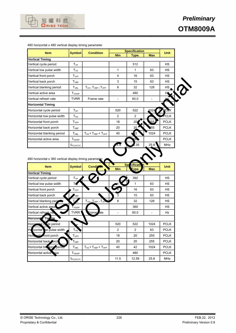
PPrreelliimmiinnaarryy
OTM8009A
© ORISE Technology Co., Ltd.
Proprietary & Confidential
226 FEB.22, 2012
Preliminary Version 0.8
480 horizontal x 480 vertical display timing parameter
Specification Item Symbol Condition
Min Type. Max Unit
Vertical Timing
Vertical cycle period TVP 512 HS
Vertical low pulse width TVS 1 1 63 HS
Vertical front porch TVFP 4 16 63 HS
Vertical back porch TVBP 3 15 63 HS
Vertical blanking period TVBL TVS + TVBP + TVFP 8 32 128 HS
Vertical active area TVDISP 480 HS
Vertical refresh rate TVRR Frame rate - 60.0 - Hz
Horizontal Timing
Horizontal cycle period THP 520 522 1024 PCLK
Horizontal low pulse width THS 2 2 63 PCLK
Horizontal front porch THFP 18 20 255 PCLK
Horizontal back porch THBP 20 20 255 PCLK
Horizontal blanking period THBL THS + THBP + THFP 40 42 1024 PCLK
Horizontal active area THDISP 480 PCLK
fPCLKCYC 14.9 16.35 25.8 MHz
480 horizontal x 360 vertical display timing parameter
Specification Item Symbol Condition
Min Type. Max Unit
Vertical Timing
Vertical cycle period TVP 392 HS
Vertical low pulse width TVS 1 1 63 HS
Vertical front porch TVFP 4 16 63 HS
Vertical back porch TVBP 3 15 63 HS
Vertical blanking period TVBL TVS + TVBP + TVFP 8 32 128 HS
Vertical active area TVDISP 360 HS
Vertical refresh rate TVRR Frame rate - 60.0 - Hz
Horizontal Timing
Horizontal cycle period THP 520 522 1024 PCLK
Horizontal low pulse width THS 2 2 63 PCLK
Horizontal front porch THFP 18 20 255 PCLK
Horizontal back porch THBP 20 20 255 PCLK
Horizontal blanking period THBL THS + THBP + THFP 40 42 1024 PCLK
Horizontal active area THDISP 480 PCLK
fPCLKCYC 11.5 12.59 25.8 MHz
ORISE Tec
h Con
fiden
tial
For IV
O Use
Only

PPrreelliimmiinnaarryy
OTM8009A
© ORISE Technology Co., Ltd.
Proprietary & Confidential
227 FEB.22, 2012
Preliminary Version 0.8
6.4.3. RGB interface power on/off sequence
The RGB interface control the normal/shutdown mode by the Sleep-out signal, the on/off sequence as shown in figure as follow.
Figure 6.4.3.1 RGB interface Power on and shutdown recovery sequence Power on and shutdown recovery sequence.
VDDVDDI
PCLK
Hsync
Vsync
Displayvoltage
Display
TSLPOUT-OFF
OFFON
1st
TOFF-VDD
Sleep-out
Figure 6.4.3.2 RGB interface Power off and shutdown sequence
Table 6.4.3.3 480 horizontal x 800 vertical display timing parameter
Parameters Symbols Min. Typ Max. Unit
VDD/VDDI-on to rising edge of Sleep-out TP-SLPOUT 5 10 - ms
PCLK input to the rising edge of Sleep-out TCLK-SLPOUT 1 - - PCLK
Rising edge of Sleep-out to display voltage ready TSLPOUT-LCD - 3 - Frame
Rising edge of Sleep-out to display on TSLPOUT-ON - 2 - Frame
Falling edge of Sleep-out to display off TSLPOUT-OFF - 5 - Frame
Input-signal-off- to VDD/VDDI-off TOFF-VDD 0 1 - us
ORISE Tec
h Con
fiden
tial
For IV
O Use
Only

PPrreelliimmiinnaarryy
OTM8009A
© ORISE Technology Co., Ltd.
Proprietary & Confidential
228 FEB.22, 2012
Preliminary Version 0.8
6.5. MPU-Series Parallel Interface
The MCU uses a 28-wires 24-data parallel interface. The chip-select CSX(active low) enables and disables the parallel interface. RESX (active low) is an external reset signal. WRX is the parallel data write, RDX is the parallel data read and D[23:0] is parallel data.
The Graphics Controller Chip reads the data at the rising edge of WRX signal. The D/CX is the data/command flag. When D/CX=’1’, D[23:0] bits are display RAM data or command parameters. When D/CX=’0’, D[23:0] bits are commands.
The 8080-series bi-directional interface can be used for communication between the micro controller and LCD driver chip. The selection of this interface is done when IM[3:0] = 0b0000.
6.5.1. Write cycle sequence
The write cycle means that the host writes information (command or/and data) to the display via the interface. Each write cycle (WRX high-low-high sequence) consists of 3 control (DCX, RDX, WRX) and data signals (DB[23:0]). DCX bit is a control signal, which tells if the data is a command or a data. The data signals are the command if the control signal is low (=’0’) and vice versa it is data (=’1’).
Note: WRX is an unsynchronized signal (It can be stopped)
The host starts to output DB[23:0] lines
when there is a falling edge of the
The display writes DB[23:0] lines when
there is a rising edge of the WRX
The host stops to output DB[23:0]
lines
WRX
DB[23:0]
Fig. 6.5.1.1 8080-Series WRX Protocol
ORISE Tec
h Con
fiden
tial
For IV
O Use
Only

PPrreelliimmiinnaarryy
OTM8009A
© ORISE Technology Co., Ltd.
Proprietary & Confidential
229 FEB.22, 2012
Preliminary Version 0.8
6.5.2. Read cycle sequence
The read cycle (RDX high-low-high sequence) means that the host reads information from display via interface. The display sends data (DB[23:0]) to the host when there is a falling edge of RDX and the host reads data when there is a rising edge of RDX.
Note: RDX is an unsynchronized signal (It can be stopped)
The display starts to control DB[23:0] lines
when there is a falling edge of the
The host reads DB[23:0] lines when
there is a rising edge of RDX
The display stops to control DB[23:0]
RDX
DB[23:0]
Fig. 6.5.2.1 8080-Series RDX Protocol
Fig. 6.5.1.2 8080-Series parallel bus protocol, Write to register or display RAM
CMD CMD PA1 CMD PAN-2 PAN-1 PPA1S Host [23:0]
‘1’ RESX
CMD CMD PA1 CMD PAN-2 PAN-1 PPA1S DB[23:0]
WRX
CSX
RDX ‘1’
DCX
1-byte 2-byte N-byte command
CMD: Write command code PA: Parameter or RAM data Signal on DB[23:0], DCX. R/WX
pins during CSX=’1’ are ignored
CMD CMD PA1 CMD PAN-2 PAN-1 PPA1S DB[23:0]
Driver [23:0]
Hi-Z
ORISE Tec
h Con
fiden
tial
For IV
O Use
Only

PPrreelliimmiinnaarryy
OTM8009A
© ORISE Technology Co., Ltd.
Proprietary & Confidential
230 FEB.22, 2012
Preliminary Version 0.8
‘1’
Fig. 6.5.2.2 8080-Series parallel bus protocol, Read data from register or display RAM
Host [23:0] Host to LCD
RESX
DB[23:0]
WRX
Driver [23:0] LCD to Host
CSX
RDX
DCX
Read Read display RAM data
CMD: Write command code PA: Parameter or RAM data
DM: Dummy
Signal on DB[23:0], DCX. R/WX, E pins during CSX=’1’
are ignored
DB[23:0]
CMD DM PA CMD data data PDMS
CMD DM PA CMD data data PDMS
Hi-Z Hi-ZCMD PCMDS
Hi-Z DM PA data data PDMS Hi-Z
ORISE Tec
h Con
fiden
tial
For IV
O Use
Only

PPrreelliimmiinnaarryy
OTM8009A
© ORISE Technology Co., Ltd.
Proprietary & Confidential
231 FEB.22, 2012
Preliminary Version 0.8
6.5.3. MPU mode color coding
Color coding uses a red [R], green [G] and blue [B] additive color mixing method. R, G and B are used for each color data index in the following sections.
6.5.3.1. 8-bit Interface color coding
12-bits/pixel (R 4-bit, G 4-bit, B 4-bit), 4,096 Colors
16-bits/pixel (R 5-bit, G 6-bit, B 5-bit), 65,536 Colors
ORISE Tec
h Con
fiden
tial
For IV
O Use
Only

PPrreelliimmiinnaarryy
OTM8009A
© ORISE Technology Co., Ltd.
Proprietary & Confidential
232 FEB.22, 2012
Preliminary Version 0.8
18-bits/pixel (R 6-bit, G 6-bit, B 6-bit), 262,144 Colors
24-bits/pixel (R 8-bit, G 8-bit, B 8-bit), 16,777,216 Colors
ORISE Tec
h Con
fiden
tial
For IV
O Use
Only

PPrreelliimmiinnaarryy
OTM8009A
© ORISE Technology Co., Ltd.
Proprietary & Confidential
233 FEB.22, 2012
Preliminary Version 0.8
6.5.3.2. 16-bit Interface color coding
12-bits/pixel (R 4-bit, G 4-bit, B 4-bit), 4,096 Colors
16-bits/pixel (R 5-bit, G 6-bit, B 5-bit), 65,536 Colors
ORISE Tec
h Con
fiden
tial
For IV
O Use
Only

PPrreelliimmiinnaarryy
OTM8009A
© ORISE Technology Co., Ltd.
Proprietary & Confidential
234 FEB.22, 2012
Preliminary Version 0.8
18-bits/pixel (R 6-bit, G 6-bit, B 6-bit), 262,144 Colors (DBIFMT = 0)
18-bits/pixel (R 6-bit, G 6-bit, B 6-bit), 262,144 Colors (DBIFMT = 1)
ORISE Tec
h Con
fiden
tial
For IV
O Use
Only

PPrreelliimmiinnaarryy
OTM8009A
© ORISE Technology Co., Ltd.
Proprietary & Confidential
235 FEB.22, 2012
Preliminary Version 0.8
24-bits/pixel (R 8-bit, G 8-bit, B 8-bit), 16,777,216 Colors (DBIFMT = 0)
24-bits/pixel (R 8-bit, G 8-bit, B 8-bit), 16,777,216 Colors (DBIFMT = 1)
6.5.3.3. 24-bit Interface color coding
ORISE Tec
h Con
fiden
tial
For IV
O Use
Only

PPrreelliimmiinnaarryy
OTM8009A
© ORISE Technology Co., Ltd.
Proprietary & Confidential
236 FEB.22, 2012
Preliminary Version 0.8
6.6. I2C-Bus Interface
6.6.1. Characteristics of I2C-bus
The I2C-bus is for bi-directional, two-line communication between different ICs or modules. The two lines compose of a serial data line (SDA) and a serial clock line (SCL). Both lines must be connected to a positive supply via a pull-up resistor. Data transfer may be initiated only when the bus is not busy.
6.6.1.1. System configuration (see figure 6.6.1.1)
(1) Transmitter: the device which sends the data to the bus
(2) Receiver: the device which receives the data from the bus
(3) Master: the device which initiates a transfer, generates clock signals and terminates a transfer
(4) Slave: the device addressed by a master
(5) Multi-Master: more than one master attempts to control the bus at the same time without corrupting the message
(6) Arbitration: procedure to ensure that, if more than one master simultaneously tries to control the bus, only one is allowed to do so and the message is not corrupted.
(7) Synchronization: procedure to synchronize the clock signals of two or more devices.
MASTERTRANSMITTER/
RECEIVER
SLAVERECEIVER
SLAVETRANSMITTER/
RECEIVER
MASTERTRANSMITTER
MASTERTRANSMITTER/
RECEIVER
SDA
SCL
Figure 6.6.1.1 System configuration
6.6.1.2. Bit transfer (See Figure 6.6.1.2)
One data bit is transferred during each clock pulse. The data on SDA line must remain stabilized during the HIGH period of the clock pulse. As changes in the data line at this time will be interpreted as a control signal.
data linestable;
data valid
changeof dataallowed
SDA
SCL
Figure 6.6.1.2 Bit transfer.
6.6.1.3. START and STOP conditions (See Figure 6.6.1.3)
Both data and clock lines remain HIGH when the bus is not busy. A HIGH-to-LOW transition on the data line, while the clock is HIGH, is defined as the START condition (S). A LOW-to-HIGH transition on the data line is defined as the STOP condition (P) while the clock is HIGH.
ORISE Tec
h Con
fiden
tial
For IV
O Use
Only

PPrreelliimmiinnaarryy
OTM8009A
© ORISE Technology Co., Ltd.
Proprietary & Confidential
237 FEB.22, 2012
Preliminary Version 0.8
S P
SDA
SCL
SDA
SCL
START condition STOP condition
Figure 6.6.1.3 Definition of START and STOP conditions.
6.6.1.4. Acknowledgment (See Figure 6.6.1.4)
Each bit in a byte (8 bits) is followed by an acknowledgment bit. The acknowledgment bit is a HIGH signal placed on the bus by the transmitter during the master generating an extra acknowledgment related clock pulse.
An addressed slave receiver must generate an acknowledgment after the reception of each byte. Also a master receiver must generate an acknowledgment after the reception of each byte that has been clocked out of the slave transmitter.
The acknowledged device must pull-down the SDA line during the acknowledgment clock pulse, so that the SDA line remains LOW during the HIGH period of the acknowledgment related clock pulse (setup and hold times must be considered).
A master receiver must signal an end of data to the transmitter by not generating an acknowledgment on the last byte that has been clocked out of the slave. In this event, the transmitter must leave the data line HIGH to enable the master to generate a stop condition.
1 2 8 9
S
STARTcondition
clock pulse foracknowledgement
SCL FROMMASTER
DATA OUTPUTBY RECEIVER
DATA OUTPUTBY TRANSMITTER
not acknowledge
acknowledge
Figure 6.6.1.4 Acknowledgement on the I2C-bus.
6.6.2. I2C-bus protocol
Before any data is transmitted on the I2C-bus, the device to respond is addressed first. Two 7-bit slave addresses (10011xx) are reserved
for the OTM8009A. The least significant bit of the slave address is set by connecting the input I2C_SA[1:0].
I2C_SA1 I2C_SA0 Slave address Notes
0 0 1001100
0 1 1001101
1 0 1001110
1 1 1001111
Other slave address
are reversed for other
IC.
Table 6.6.2.1 Reserve address for OTM8009A.
ORISE Tec
h Con
fiden
tial
For IV
O Use
Only

PPrreelliimmiinnaarryy
OTM8009A
© ORISE Technology Co., Ltd.
Proprietary & Confidential
238 FEB.22, 2012
Preliminary Version 0.8
6.6.2.1. I2C-bus Write Instruction and parameter
OTM8009A supports register write sequence via I2C-bus transfer. The detail transference sequences are illustrated and described as below.
(1) Data transfers for register writing follow the format is shown in Figure 6.6.2.1.
(2) After the START condition (Str), a slave address is sent. R/W bit is setting to "zero" for WRITE.
(3) The slave issues an ACK to master.
(4) 16 bits register high byte address transfer first. Then transfer the register low byte address.
(5) 16 bits register high byte data of parameter transfer first. Then transfer the register low byte data parameter .
(6) A data transfer is always terminated by a STOP condition.
Figure 6.6.2.1 I2C write stream for write command
6.6.2.2. I2C-bus Write GRAM
Figure 6.6.2.2 Color format and I2C write stream
Note :
(1) 4096 color : 3 bytes = 2 pixels
(2) 65536 color: 2 bytes = 1 pixel
(3) 262K color: 3bytes = 1 pixel
(4) 16.7M color: 3bytes = 1 pixel
(5) 8 color(idle mode): 1 byte = 2 pixel
6.6.2.3. I2C-bus read 7 6 5 4 3 2 1 0 7 6 5 4 3 2 1 0 7 6 5 4 3 2 1 0 7 6 5 4 3 2 1 0 7 6 5 4 3 2 1 0 7 6 5 4 3 2 1 0
D7 D6 D5 D4 D3 D2 D1 D0 D7 D6 D5 D4 D3 D2 D1 D0 D7 D6 D5 D4 D3 D2 D1 D0 D7 D6 D5 D4 D3 D2 D1 D0 D7 D6 D5 D4 D3 D2 D1 D0 D7 D6 D5 D4 D3 D2 D1 D0
W R
7 6 5 4 3 2 1 0 7 6 5 4 3 2 1 0 7 6 5 4 3 2 1 0 7 6 5 4 3 2 1 0 7 6 5 4 3 2 1 0 7 6 5 4 3 2 1 0
D7 D6 D5 D4 D3 D2 D1 D0 D7 D6 D5 D4 D3 D2 D1 D0 D7 D6 D5 D4 D3 D2 D1 D0 D7 D6 D5 D4 D3 D2 D1 D0 D7 D6 D5 D4 D3 D2 D1 D0 D7 D6 D5 D4 D3 D2 D1 D0
W R
7 6 5 4 3 2 1 0 7 6 5 4 3 2 1 0 7 6 5 4 3 2 1 0
D7 D6 D5 D4 D3 D2 D1 D0 D7 D6 D5 D4 D3 D2 D1 D0 D7 D6 D5 D4 D3 D2 D1 D0
262K color R1[5] R1[4] R1[3] R1[2] R1[1] R1[0] X X G1[5] G1[4] G1[3] G1[2] G1[1] G1[0] X X B1[5] B1[4] B1[3] B1[2] B1[1] B1[0] X X
16.7M color R1[7] R1[6] R1[5] R1[4] R1[3] R1[2] R1[1 R1[0] G1[7] G1[6] G1[5] G1[4] G1[3] G1[2]G1[1 G1[0] B1[7] B1[6] B1[5] B1[4] B1[3] B1[2] B1[1 B1[0]
Ack
Dummy[7:0]
dummy
dummy
EndAck Ack End StrStr Ack Ack
ID[6:0]=10011xx Parameter1[7:0]
Ack
Parameter2[7:0]
End Str Ack
Instruction Address[7:0]
Str Ack Ack
Instruction Address[7:0] = 00h
Ack
Ack
Dummy[15:8]
Data[7:0]
dummy
Data[7:0]
Ack End
dummy
Data[7:0]
Ack
ID[6:0]=10011xx
ID[6:0]=10011xx
ID[6:0]=10011xx
Ack
Instruction Address[15:8]
Ack
Instruction Address = 2E/3E
Read Instruction+1 Parameter
Read GRAM
Figure 6.6.2.3 Color format and I2C read stream
Note : OTM8009A only support 16.7M / 262K color for GRAM read back.
ORISE Tec
h Con
fiden
tial
For IV
O Use
Only

PPrreelliimmiinnaarryy
OTM8009A
© ORISE Technology Co., Ltd.
Proprietary & Confidential
239 FEB.22, 2012
Preliminary Version 0.8
6.7. Serial interface (SPI)
The selection of this interface is done by set IM2 / IM1 / IM0 = 011. And select IM3 = 0 or 1 to decide the trigger edge of serial
clock (SCL) is rising edge or falling edge. The serial interface is used to communication between the micro controller and the LCD
driver chip. It contains CSX (chip select), SCL (serial clock), SDI (serial data input) and SDO (serial data output). Serial clock
(SCL) is used for interface with MPU only, so it can be stopped when no communication is necessary. If the host places the SDI
line into high-impedance state during the read intervals, then the SDI and SDO can be tied together.
6.7.1. SPI Write Mode
The write mode of the interface means the micro controller writes commands and data to the OTM8009A. The serial interface is
initialized when CSX is high. In this state, SCL clock pulse or SDI data have no effect. A falling edge on CSX enables the serial
interface and indicates the start of data transmission.
When CSX is high, SCL clock is ignored. During the high time of CSX the serial interface is initialized. At the falling CSX edge,
SCL can be high or low (See Figure 6.7.1.1). SDI / SDO is sampled at the rising edge of SCL. R/W indicates, whether the byte is read
command (R/W = '1') or write command (R/W = '0'). It is sampled when first rising SCL edge. If CSX stays low after the last bit of
command/data byte, the serial interface expects the R/W bit of the next byte at the next rising edge of SCL.
Figure 6.7.1.1 SPI Protocol for register write mode
ORISE Tec
h Con
fiden
tial
For IV
O Use
Only

PPrreelliimmiinnaarryy
OTM8009A
© ORISE Technology Co., Ltd.
Proprietary & Confidential
240 FEB.22, 2012
Preliminary Version 0.8
Figure 6.7.1.2 SPI Protocol for GRAM write (Separate byte mode)
Table 6.7.1.3 Available color format for SPI interface
ORISE Tec
h Con
fiden
tial
For IV
O Use
Only

PPrreelliimmiinnaarryy
OTM8009A
© ORISE Technology Co., Ltd.
Proprietary & Confidential
241 FEB.22, 2012
Preliminary Version 0.8
6.7.2. SPI Read Mode
The read mode of the interface means that the micro controller reads register value from the OTM8009A. To do so the micro controller first
has to send a command and then the following byte is transmitted in the opposite direction. After that CSX is required to go high before a
new command is send (see Figure. 6.7.2.1). The OTM8009A samples the SDI (input data) at the rising edges, but shifts SDO (output data)
at the falling SCL edges. Thus the micro controller is supported to read data at the rising SCL edges. After the read status command has
been sent, the SDI line must be set to tri-state no later than at the falling SCL edge of the last bit. For the memory data read, a dummy
clock cycle is needed (16 SCL clocks) to wait the memory data send out in SPI interface. But it doesn't need any dummy clock when
execute the command data read.
Figure 6.7.2.1 SPI Protocol for register read mode
ORISE Tec
h Con
fiden
tial
For IV
O Use
Only

PPrreelliimmiinnaarryy
OTM8009A
© ORISE Technology Co., Ltd.
Proprietary & Confidential
242 FEB.22, 2012
Preliminary Version 0.8
Figure 6.7.2.2 SPI Protocol for GRAM read
ORISE Tec
h Con
fiden
tial
For IV
O Use
Only

PPrreelliimmiinnaarryy
OTM8009A
© ORISE Technology Co., Ltd.
Proprietary & Confidential
243 FEB.22, 2012
Preliminary Version 0.8
6.8. Sleep Out-Command And Self-Diagnostic Functions Of The Display Module
6.8.1. Register loading detection
Sleep Out-command is a trigger for an internal function of the display module, which indicates, if the display module loading function of
factory default values from OTP (one-time programming memory) to registers of the display controller is working properly.
There are compared factory values of the OTP and register values of the display controller by the display controller. If those both values
(OTP and register values) are same, there is inverted (=increased by 1) a bit in “Read Display Self-Diagnostic Result (0Fh)” (=RDDSDR)
(The used bit of this command is D7). If those both values are not same, this bit (D7) is not inverted (= increased by 1).
The flow chart for this internal function is following:
Note: There is not compared and loaded register values, which can be changed by user (00h to AFh and DAh to DDh), by the display module.
Sleep In (10h)
Sleep Out Mode Sleep In Mode
Sleep Out (11h)
Compares OTP and register values
Are OTP and register values same ?
D7 inverted
RDDSDR’s D7=0
Power on sequence HW reset SW reset
Yes
No
Loads values from OTP to registers
ORISE Tec
h Con
fiden
tial
For IV
O Use
Only

PPrreelliimmiinnaarryy
OTM8009A
© ORISE Technology Co., Ltd.
Proprietary & Confidential
244 FEB.22, 2012
Preliminary Version 0.8
6.8.2. Functionality detection
Sleep Out-command is a trigger for an internal function of the display module, which indicates, if the display module is still running and
meets functionality requirements.
The internal function (= the display controller) is comparing, if the display module is still meeting functionality requirements (only Booster
voltage level). If functionality requirement is met, there is inverted (= increased by 1) a bit in “Read Display Self- Diagnostic Result (0Fh)” (=
RDDSDR) (The used bit of this command is D6). If functionality requirement is not same, this bit (D6) is not inverted (= increased by 1).
The flow chart for this internal function is following:
Note: There is needed 120msec after Sleep Out -command, when there is changing from Sleep In –mode to Sleep Out -mode, before there is possible to check if functionality requirements are met and a value of RDDSDR’s D6 is valid. Otherwise, there is 5msec delay for D6’s value, when Sleep Out –command is sent in Sleep Out -mode.
Sleep In (10h)
Sleep Out Mode Sleep In Mode
Sleep Out (11h)
Checks Booster voltage levels and other functionalities
Is functionality requirement met ?
D6 inverted
RDDSDR’s D6=0
Power on sequence HW reset SW reset
Yes
No
ORISE Tec
h Con
fiden
tial
For IV
O Use
Only

PPrreelliimmiinnaarryy
OTM8009A
© ORISE Technology Co., Ltd.
Proprietary & Confidential
245 FEB.22, 2012
Preliminary Version 0.8
6.9. Power On/Off Sequence
VDDIO and VDD can be applied in any order.
VDDIO and VDD can be powered down in any order.
During power off, if LCD is in the Sleep Out mode, VDD and VDDIO must be powered down minimum 120msec after RESX has been
released.
During power off, if LCD is in the Sleep In mode, VDDIO or VDD can be powered down minimum 0msec after RESX has been released.
CSX can be applied at any timing or can be permanently grounded. RESX has priority over CSX.
Note 1: There will be no damage to the display module if the power sequences are not met.
Note 2: There will be no abnormal visible effects on the display panel during the Power On/Off Sequences.
Note 3: There will be no abnormal visible effects on the display between end of Power On Sequence and before receiving Sleep Out command. Also between
receiving Sleep In command and Power Off Sequence.
If RESX line is not held stable by host during Power On Sequence, then it will be necessary to apply a Hardware Reset (RESX) after Host
Power On Sequence is complete to ensure correct operation. Otherwise function is not guaranteed.
The power on/off sequence is illustrated below:
6.9.1. Case 1 – RESX line is held high or unstable by host at power on
If RESX line is held High or unstable by the host during Power On, then a Hardware Reset must be applied after both VDD and VDDIO
have been applied – otherwise correct functionality is not guaranteed. There is no timing restriction upon this hardware reset.
TrPW = +/- no limit tfPW = +/- no limit
Time when the latter signal rises up to 90% of its Typical Value. e.g. When VDD2 comes later, This time is defined at the cross point of 90% of 2.5V/2.75V, not 90% of 2.3V.
trPW!CS = +/- no limittfPW!CS = +/- no limit
Time when the former signal falls down to 90% of its Typical Value.e.g. When VDD2 falls earlier, This time is defined at the cross point of 90% of 2.5V/2.75V, not 90% of 2.3V.
VDD1
VDD2
!CS
Note: Unless otherwise specified, timings herein show cross point at 50% of signal/power level.
H or L
!RES
trPW!RES = + no limit
tfPW!RES1 = min.120ms
tfPW!RES2 = min.0ns
tfPW!RES1 is applied to !RES falling in the Sleep Out Mode. tfPW!RES2 is applied to !RES falling in the Sleep In Mode.
30%
!RES 30%
(Power down in Sleep Out mode)
(Power down in Sleep In mode)
trPW!RES = + no limit
VDDI
VDD
CSX
RESX
RESX
RESX
RESX
CSX
RESX
RESX1
CSX
RESX2
TfpwRESX1 TfpwRESX2
RES
2.75V,not 90% of
2.75V,not 90% of ORISE Tec
h Con
fiden
tial
For IV
O Use
Only

PPrreelliimmiinnaarryy
OTM8009A
© ORISE Technology Co., Ltd.
Proprietary & Confidential
246 FEB.22, 2012
Preliminary Version 0.8
6.9.2. Case 2– RESX line is held low by host at power on
If RESX line is held Low (and stable) by the host during Power On, then the RESX must be held low for minimum 10sec after both VDD
and VDDIO have been applied.
6.9.3. Uncontrolled power off
The uncontrolled power off means a situation when e.g. there is removed a battery without the controlled power off sequence. There will
not be any damages for the display module or the display module will not cause any damages for the host or lines of the interface.
At an uncontrolled power off the display will go blank and there will not be any visible effects within (TBD) second on the display (blank
display) and remains blank until “Power On Sequence” powers it up.
TrPW = +/- no limit tfPW = +/- no limit
Time when the latter signal rises up to 90% of its Typical Value. e.g. When VDD2 comes later, This time is defined at the cross point of 90% of 2.5V/2.75V, not 90% of 2.3V.
trPW!CS = +/- no limittfPW!CS = +/- no limit
Time when the former signal falls down to 90% of its Typical Value.e.g. When VDD2 falls earlier, This time is defined at the cross point of 90% of 2.5V/2.75V, not 90% of 2.3V.
VDD1
VDD2
!CS
Note: Unless otherwise specified, timings herein show cross point at 50% of signal/power level.
H or L
!RES
trPW!RES = min.10s
tfPW!RES1 = min.120ms
tfPW!RES2 = min.0ns
tfPW!RES1 is applied to !RES falling in the Sleep Out Mode. tfPW!RES2 is applied to !RES falling in the Sleep In Mode.
!RES
(Power down in Sleep Out mode)
(Power down in Sleep In mode)
trPW!RES = min.10s
VDDI
VDD
CSX
RESX
RESX
RESX RESX
RESX2
CSX
CSX
RESX
RESX1
RESX
TfpwRESX1 TfpwRESX2
2.75V,not 90% of
2.75V,not 90% of
ORISE Tec
h Con
fiden
tial
For IV
O Use
Only

PPrreelliimmiinnaarryy
OTM8009A
© ORISE Technology Co., Ltd.
Proprietary & Confidential
247 FEB.22, 2012
Preliminary Version 0.8
6.10. Power Level Definition
6.10.1. Power level
6 level modes are defined they are in order of Maximum Power consumption to Minimum Power Consumption:
1. Normal Mode On (full display), Idle Mode Off, Sleep Out.
In this mode, the display is able to show maximum 262,144 colors.
2. Partial Mode On, Idle Mode Off, Sleep Out.
In this mode part of the display is used with maximum 262,144 colors.
3. Normal Mode On (full display), Idle Mode On, Sleep Out.
In this mode, the full display area is used but with 8 colors.
4. Partial Mode On, Idle Mode On, Sleep Out.
In this mode, part of the display is used but with 8 colors.
5. Sleep In Mode
In this mode, the DC: DC converter, Internal oscillator and panel driver circuit are stopped. Only the MCU interface and memory works
with VDDIO power supply. Contents of the memory are safe.
6. Power Off Mode
In this mode, both VDD and VDDIO are removed.
Note: Transition between modes 1-5 is controllable by MCU commands. Mode 6 is entered only when both Power supplies are removed.
ORISE Tec
h Con
fiden
tial
For IV
O Use
Only

PPrreelliimmiinnaarryy
OTM8009A
© ORISE Technology Co., Ltd.
Proprietary & Confidential
248 FEB.22, 2012
Preliminary Version 0.8
6.10.2. Power flow chart
PTLON
NORON
NORON
PTLON
Sleep out Normal display mode on
Idle mode on
Sleep out Normal display mode on
Idle mode off
Sleep out Partial mode on
Idle mode on
Sleep out Partial mode on
Idle mode off
Sleep inNormal display mode on
Idle mode off
Sleep inNormal display mode on
Idle mode on
Sleep inPartial mode on
Idle mode on
Sleep inPartial mode on
Idle mode off
SLPIN
SLPOUT
IDMON IDMOFF IDMON IDMOFF
Power on sequence HW reset SW reset
Normal display mode on = NORON Partial mode on = PTLON Idle mode off = IDMOFF Idle mode on = IDMON Sleep out = SLPOUT Sleep in = SLPIN
IDMON IDMOFF IDMON IDMOFF
SLPIN
SLPOUT
SLPIN
SLPOUT
SLPIN
SLPOUT
PTLON
NORON
NORON
PTLON
Sleep out Sleep in
Note 1: There is not any abnormal visual effect when there is changing from one power mode to another power mode.
Note 2: There is not any limitation, which is not specified by this spec, when there is changing from one power mode to another power mode.
ORISE Tec
h Con
fiden
tial
For IV
O Use
Only

PPrreelliimmiinnaarryy
OTM8009A
© ORISE Technology Co., Ltd.
Proprietary & Confidential
249 FEB.22, 2012
Preliminary Version 0.8
6.11. Tear Effect Information
6.11.1. General
The MCU is updating the frame memory of the display module via its interface (DSI).
The display module is refreshing the display panel from the frame memory independently and it does not know what is happening on
the interface of the display module (The MCU is sending image information to the display module). It is possible that this asynchronous
updating is causing an abnormal visual effect on the display panel of the display module.
Therefore, the display module is sending a synchronous information (= Tearing Effect Information), which is telling the position of the
refreshing on the display panel, to the MCU which can decide when it can send image information to the display module (Mainly used for a
moving image e.g. video clips) that there can avoid the abnormal visual effect on the display panel of the display module.
This Tearing Effect information can be sent in two different ways:
• Separated Line, which is so-called Tearing Effect (TE) line
• Bus, which is so-called Tearing Effect (TEE) Bus Trigger, when the display module is sending a trigger to the MCU
The TE line can be used in DSI case if the Tearing Effect (TEE) bus trigger is not possible to use and the Tearing Effect (TEE) Bus
Trigger is only used in DSI case.
6.11.1.1. Tearing effect line models
The Tearing Effect line supplies to the MCU a Panel synchronisation signal and this signal can be enabled or
disabled by the Tearing Effect Line Off & On commands.
The mode of the Tearing Effect Signal is defined by the Parameter of the Tearing Effect Line On command.
Mode 1:The Tearing Effect Output signal consists of V-Sync information only:
tvdh = The display panel is not updated from the Frame Memory.
tvdl = The display panel is updated from the Frame Memory (except Invisible Line – see below).
Mode 2:The Tearing Effect Output signal consists of V-Sync and H-Sync information; There is one V-sync and 864 H-sync pulses per field:
tvdh = The display panel is not updated from the Frame Memory.
tvdl = The display panel is updated from the Frame Memory (except Invisible Line – see below).
ORISE Tec
h Con
fiden
tial
For IV
O Use
Only

PPrreelliimmiinnaarryy
OTM8009A
© ORISE Technology Co., Ltd.
Proprietary & Confidential
250 FEB.22, 2012
Preliminary Version 0.8
TE Line mode1 and Mode2 is shown as below graph:
Note: During Sleep In Mode, the Tearing Effect Output Pin is active Low.
6.11.1.2. Tearing effect line timing
The Tearing Effect signal is described below:
Idle Mode Off/On
Symbol Parameter Min. Max. Unit
tvdl Vertical Timing Low Duration ms
tvdh Vertical Timing High Duration 1000 μs
thdl Horizontal Timing Low Duration - μs
thdh Horizontal Timing High Duration 500 μs
1. Minimum frequency of the TE-line cannot be less than 25Hz, when the TE-line is active, on Mode 1.
2. The signal’s rise and fall times (tf, tr) are stipulated to be equal to or less than 15ns when the maximum load is TBD Ω.
ORISE Tec
h Con
fiden
tial
For IV
O Use
Only

PPrreelliimmiinnaarryy
OTM8009A
© ORISE Technology Co., Ltd.
Proprietary & Confidential
251 FEB.22, 2012
Preliminary Version 0.8
The TE signal rising and falling timing is described below:
6.11.1.3. Example 1 MCU write is faster then panel read
MCU write is faster then panel read
Data write to Frame Memory is now synchronised to the Panel Scan. It should be written during the vertical sync pulse of the Tearing
Effect Output Line. This ensures that data is always written ahead of the panel scan and each Panel Frame refresh has a complete new
image:
Example 1 – Image on the display panel
ORISE Tec
h Con
fiden
tial
For IV
O Use
Only

PPrreelliimmiinnaarryy
OTM8009A
© ORISE Technology Co., Ltd.
Proprietary & Confidential
252 FEB.22, 2012
Preliminary Version 0.8
6.11.1.4. Example 1 MCU write is slower then panel read
MCU write is faster then panel read
The MCU to Frame Memory write begins just after Panel Read has commenced i.e. after one horizontal sync pulse of the Tearing Effect
Output Line. This allows time for the image to download behind the Panel Read pointer and finishing download during the subsequent
frame before the Read Pointer “catches” the MCU to frame memory write position.
Example 2 – Image on the display panel
ORISE Tec
h Con
fiden
tial
For IV
O Use
Only

PPrreelliimmiinnaarryy
OTM8009A
© ORISE Technology Co., Ltd.
Proprietary & Confidential
253 FEB.22, 2012
Preliminary Version 0.8
6.11.2. Tearing effect bus trigger
A Tearing Effect Bus Trigger information supplies to the MCU a Panel synchronisation trigger and this Tearing Effect Bus Trigger
information can be enabled or disabled by commands “Tearing Effect Line Off (34h)” and “Tearing Effect Line On (35h)” when the only
mode of the Tearing Effect Signal is VSync. information.
The display module is sending this trigger information in Escape Mode after the Bus Turnaround (BTA). The Tearing Effect Bus Trigger
can only use in DSI case without the TE line.
A rising edge of the V-Sync and DSI-D0
ORISE Tec
h Con
fiden
tial
For IV
O Use
Only

PPrreelliimmiinnaarryy
OTM8009A
© ORISE Technology Co., Ltd.
Proprietary & Confidential
254 FEB.22, 2012
Preliminary Version 0.8
6.11.2.1. Tearing effect bus trigger enable
The MCU can enable the Tearing Effect Bus Trigger on the display module in 2 different ways when a Short Packet (SPa) or Long
Packet (LPa) is used. These cases are illustrated below.
Tearing effect bus trigger enable (DCSW1-S) – short packet (SPa)
Tearing effect bus trigger enable (DCSW-L) – long packet (LPa)
ORISE Tec
h Con
fiden
tial
For IV
O Use
Only

PPrreelliimmiinnaarryy
OTM8009A
© ORISE Technology Co., Ltd.
Proprietary & Confidential
255 FEB.22, 2012
Preliminary Version 0.8
6.11.2.2. Tearing effect bus trigger disable
The MCU can enable the Tearing Effect Bus Trigger on the display module in 2 different ways when a Short Packet (SPa) or Long
Packet (LPa) is used. These both possibilities are illustrated below.
Tearing effect bus trigger disable (DCSWN-S) – short packet (SPa)
Tearing effect bus trigger disable (DCSW-L) – long packet (LPa)
ORISE Tec
h Con
fiden
tial
For IV
O Use
Only

PPrreelliimmiinnaarryy
OTM8009A
© ORISE Technology Co., Ltd.
Proprietary & Confidential
256 FEB.22, 2012
Preliminary Version 0.8
6.11.2.3. Tearing effect bus trigger sequences
6.11.2.4. Tearing effect bus trigger enable sequence – DCSW-L and HSDT
Notes:
1. Lines 1 – 17 are needed for every frame..
2. Bits 5 and 7 of the AwER are applied.
ORISE Tec
h Con
fiden
tial
For IV
O Use
Only
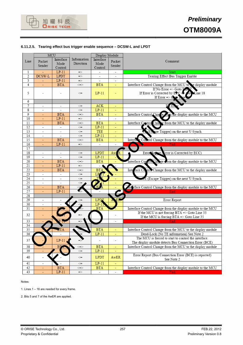
PPrreelliimmiinnaarryy
OTM8009A
© ORISE Technology Co., Ltd.
Proprietary & Confidential
257 FEB.22, 2012
Preliminary Version 0.8
6.11.2.5. Tearing effect bus trigger enable sequence – DCSW-L and LPDT
Notes:
1. Lines 1 – 16 are needed for every frame.
2. Bits 5 and 7 of the AwER are applied.
ORISE Tec
h Con
fiden
tial
For IV
O Use
Only

PPrreelliimmiinnaarryy
OTM8009A
© ORISE Technology Co., Ltd.
Proprietary & Confidential
258 FEB.22, 2012
Preliminary Version 0.8
6.11.2.6. Tearing effect bus trigger enable sequence – DCSW1-S and HPDT
Notes:
1. Lines 1 – 17 are needed for every frame.
2. Bits 5 and 7 of the AwER are applied.
ORISE Tec
h Con
fiden
tial
For IV
O Use
Only

PPrreelliimmiinnaarryy
OTM8009A
© ORISE Technology Co., Ltd.
Proprietary & Confidential
259 FEB.22, 2012
Preliminary Version 0.8
6.11.2.7. Tearing effect bus trigger enable sequence – DCSW1-S and LPDT
Notes:
1. Lines 1 – 16 are needed for every frame.
2. Bits 5 and 7 of the AwER are applied.
ORISE Tec
h Con
fiden
tial
For IV
O Use
Only

PPrreelliimmiinnaarryy
OTM8009A
© ORISE Technology Co., Ltd.
Proprietary & Confidential
260 FEB.22, 2012
Preliminary Version 0.8
6.11.2.8. Tearing effect bus trigger enable sequence – DCSWN-S and HPDT
6.11.2.9. Tearing effect bus trigger enable sequence – DCSWN-S and LPDT
ORISE Tec
h Con
fiden
tial
For IV
O Use
Only

PPrreelliimmiinnaarryy
OTM8009A
© ORISE Technology Co., Ltd.
Proprietary & Confidential
261 FEB.22, 2012
Preliminary Version 0.8
6.12. Checksum
The display module consists of two 8-bit checksum registers, which are used checksum calculations for area registers (includes the
frame memory), on the display module. Area registers are registers which values can change a command directly. One of the checksum
registers is “First Checksum” (FCS) and another is “Continue Checksum” (CCS). These register values are set to 00h as an initial value
when there is started to calculate a new checksum. The display module is starting to calculate the new checksum after there is a write
access on area registers. This means that read commands are not used as a calculation starting trigger in this case. The checksum
calculation is always interrupted, when there is a new write access on area registers. The checksum calculation is also started from the
beginning. The result of the first finished checksum calculation is stored on the FCS register, which value is kept until
there is the new write access on area registers and the new checksum value is calculated in the first time again.
The maximum time, when the FCS is readable, is 150ms after there is the last write access on area registers.
The checksum calculation is continuing after the finished first checksum calculation where the FCS has gotten the checksum value. These
new checksum values are always stored on CCS register (Old value is replaced a new one) after the last area register has been calculated
to the checksum.
The maximum time, when the CCS is readable in the first time, is 300ms after there is the last write access on area registers.
There is always updated a checksum comparison bit (See command “Read Display Self-Diagnostic Result (0FH)” and bit D0) when there is
compared FCS and CCS checksums after a new checksum value is stored on CCS.
The maximum time, when the comparison has been done between FCS and CCS in the first time, is 300ms then the comparison has
been done in every 150ms (this is maximum time). Area can read FCS, CCS and Comparison bit D0 values. See command: “Read First
Checksum (AAH)”, “Read Continue Checksum (AFH)” and ”Read Display Self-Diagnostic Result (0FH)”.
There can be an overflow during a checksum calculation. These overflow bits are not needed to store anywhere. This means that these
overflow bits can be ignored by the display module.
An example of the checksum calculation:
- Register Values: A1h, 12h, 81h, DEh, F2h
- Calculated Value: 304h (= A1h + 12h + 81h + DEh + F2h)
- Ignored Bits: 3h
- Stored Checksum: 04h
This checksum calculation function is only running in “Sleep Out” mode and it is stopped in “Sleep In” mode.
ORISE Tec
h Con
fiden
tial
For IV
O Use
Only

PPrreelliimmiinnaarryy
OTM8009A
© ORISE Technology Co., Ltd.
Proprietary & Confidential
262 FEB.22, 2012
Preliminary Version 0.8
Checksum Sequence
Notes:
1. This function is restarted at Step 1 if there is any write action on area registers.
2. These time can be shorter on the display module.
ORISE Tec
h Con
fiden
tial
For IV
O Use
Only

PPrreelliimmiinnaarryy
OTM8009A
© ORISE Technology Co., Ltd.
Proprietary & Confidential
263 FEB.22, 2012
Preliminary Version 0.8
6.13. Content Adaptive Brightness Control (CABC)
Content adaptation means that content grey level scale can be increased while simultaneously lowering brightness of the backlight to achieve same perceived brightness. CABC block diagram is shown as below:
6.13.1. Backlight(BC) brightness control
Use the PWM output to control backlight. BC timing is described as below graph:
Symbol Definition MIN Max. Unit
tpw Pulse Width 0.033 8.33 ms
Fpw PWM Frequency 38 39k Hz
ORISE Tec
h Con
fiden
tial
For IV
O Use
Only

PPrreelliimmiinnaarryy
OTM8009A
© ORISE Technology Co., Ltd.
Proprietary & Confidential
264 FEB.22, 2012
Preliminary Version 0.8
6.14. NVM Programming Procedure
6.14.1. NVM program flow chart
EXTC pin high
Check registers
Check registers
Power On Sequence Apply VDDI/ VDD
Wait 700 us for power on reset
Hardware ResetWait for 2ms otp reload
CMD2 enable(CMD FF00h)
ORISE CMD enable(CMD FF80h)
Set ID1 Data(CMD D000h)Set ID2 Data
(CMD D100h)Set ID3 Data
(CMD D101h)
Set Gamma 2.2 +(CMD E100h )
Set Gamma 2.2 -(CMD E200h)
Set analog voltage(CMD D800h)
SLPIN( CMD 10h)
Set Standby modeWait more than 80ms
Apply 7.5 V at MTP_ powerWait 100 ms for voltage
stable
NVMINProgram on
(CMD EB00h)Wait 850 ms (min)
NVMOUTProgram end
(CMD EB00h)Set NVM Write Disable
Remove 7.5 V at MTP_ power
Hardware ResetWait for ms otp reload
SLPOUT( CMD 11h)
Set Normal operation
Normally Display
SLPOUT( CMD 11h)
Set Normal OperationWait 5ms
Set ID1 Data(CMD D000h)Set ID2 Data
(CMD D100h)Set ID3 Data
(CMD D100h)
Set Gamma 2.2 +(CMD E100h)
Set Gamma 2.2 -( CMD E200h)
Set analog voltage(CMD D800h)
Set ID1 Data(CMD D000h)Set ID2 Data
(CMD D100h)Set ID3 Data
(CMD D101h)
Set Gamma 2.2 +(CMD E100h)
Set Gamma 2.2 -( CMD E200h)
Set analog voltage(CMD D800h)
Write registers
Set panel timing(CMD Cx00h )
Set panel timing(CMD Cx00h)
Set panel timing(CMD Cx00h)
2
ORISE Tec
h Con
fiden
tial
For IV
O Use
Only

PPrreelliimmiinnaarryy
OTM8009A
© ORISE Technology Co., Ltd.
Proprietary & Confidential
265 FEB.22, 2012
Preliminary Version 0.8
6.14.2. Programming sequence
Figure 6.9.1 shows the sequence about NVM. The first step to program NVM is “write Standby operation command”. After this command,
over than 50ms must be hold to make sure that the dirver IC is in Standby mode. Another 100ms is necessary to make sure NVMD is
stable to 7.5V. NVM program command can be written after stable 7.5V voltage existed. Then, NVM Program End command is written after
850ms. 7.5V voltage is removed after Program End command, and then Normal operation command is written to verify the NVM memory.
$10(S
ET
Standby
operation)
`Go
toStandby!!
Apply
7.5Vto
NV
MD
Rem
ove7.5V
> 50ms
$E(O
TP
Program
Start)
$(O
TP
Program
End)
> 100ms > 10ms > 10ms
OTP Program period
7.5V Enable period
Time $1(S
ET
Norm
aloperation)
1B
EB
ORISE Tec
h Con
fiden
tial
For IV
O Use
Only

PPrreelliimmiinnaarryy
OTM8009A
© ORISE Technology Co., Ltd.
Proprietary & Confidential
266 FEB.22, 2012
Preliminary Version 0.8
7. ELECTRICAL SPECIFICATIONS
7.1. Absolute Maximum Ratings
Parameter Symbol Rating Unit
Power Supply for I/O VDDIO-VSS -0.3~+4.5 V
Power Supply for HISSI Interface VDDAM-AVSS -0.3~+6.0 V
Power Supply for logic power regulator VCC-VSS -0.3~+6.0 V
Power Supply for Analog circuit VDD-AVSS -0.3~+6.0 V
Power Supply for OTP MTP_PWR-AVSS -0.3~+7.8 V
I/O input Voltage Vt -0.3~VDDIO+0.3 V
Driver output voltage VGH-VGL -0.3~+32 V
Differential Input Voltage
HSSI_CLK_P/N
HSSI_D0_P/N
HSSI_D1_P/N
-0.3~1.8 V
Operating Temperature Topr -30~+70
Storage Temperature Tstg -30~+85
Note1. The maximum applicable voltage on any pin with respect to 0V.
Note2. Device is subject to be damaged permanently if stresses beyond those absolute maximum ratings listed above.
ORISE Tec
h Con
fiden
tial
For IV
O Use
Only
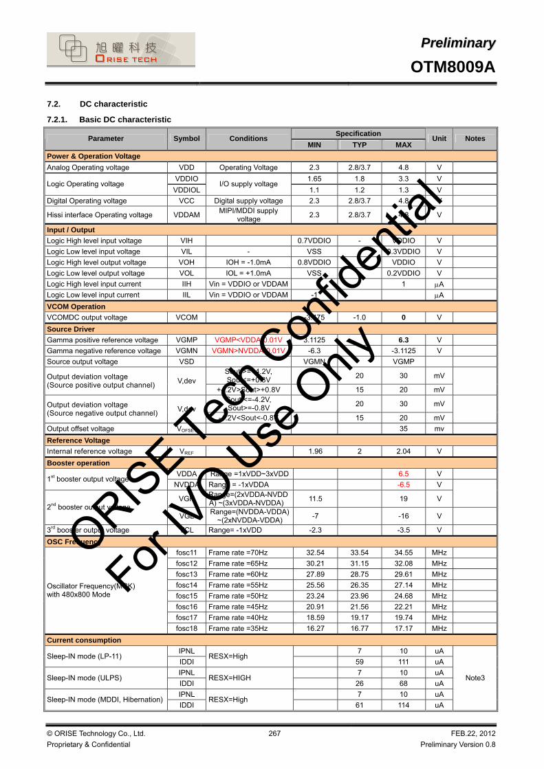
PPrreelliimmiinnaarryy
OTM8009A
© ORISE Technology Co., Ltd.
Proprietary & Confidential
267 FEB.22, 2012
Preliminary Version 0.8
7.2. DC characteristic
7.2.1. Basic DC characteristic
Specification Parameter Symbol Conditions
MIN TYP MAX Unit Notes
Power & Operation Voltage
Analog Operating voltage VDD Operating Voltage 2.3 2.8/3.7 4.8 V
VDDIO 1.65 1.8 3.3 V Logic Operating voltage
VDDIOL I/O supply voltage
1.1 1.2 1.3 V
Digital Operating voltage VCC Digital supply voltage 2.3 2.8/3.7 4.8 V
Hissi interface Operating voltage VDDAM MIPI/MDDI supply
voltage 2.3 2.8/3.7 4.8 V
Input / Output
Logic High level input voltage VIH 0.7VDDIO - VDDIO V
Logic Low level input voltage VIL - VSS - 0.3VDDIO V
Logic High level output voltage VOH IOH = -1.0mA 0.8VDDIO - VDDIO V
Logic Low level output voltage VOL IOL = +1.0mA VSS - 0.2VDDIO V
Logic High level input current IIH Vin = VDDIO or VDDAM 1 A
Logic Low level input current IIL Vin = VDDIO or VDDAM -1 A
VCOM Operation
VCOMDC output voltage VCOM -3.475 -1.0 0 V
Source Driver
Gamma positive reference voltage VGMP VGMP<VDDA-0.01V 3.1125 6.3 V
Gamma negative reference voltage VGMN VGMN>NVDDA-0.01V -6.3 -3.1125 V
Source output voltage VSD VGMN VGMP Sout >=+4.2V, Sout<=+0.8V
20 30 mV Output deviation voltage (Source positive output channel)
V,dev +4.2V>Sout>+0.8V 15 20 mV
Sout <=-4.2V, Sout>=-0.8V
20 30 mV Output deviation voltage (Source negative output channel)
V,dev -4.2V<Sout<-0.8V 15 20 mV
Output offset voltage VOFSET 35 mv
Reference Voltage
Internal reference voltage VREF 1.96 2 2.04 V
Booster operation
VDDA Range =1xVDD~3xVDD 6.5 V 1st booster output voltage
NVDDA Range = -1xVDDA -6.5 V
VGH Range=(2xVDDA-NVDDA) ~(3xVDDA-NVDDA)
11.5 19 V
2nd booster output voltage VGL
Range=(NVDDA-VDDA) ~(2xNVDDA-VDDA)
-7 -16 V
3rd booster output voltage VCL Range= -1xVDD -2.3 -3.5 V
OSC Frequency
fosc11 Frame rate =70Hz 32.54 33.54 34.55 MHz
fosc12 Frame rate =65Hz 30.21 31.15 32.08 MHz
fosc13 Frame rate =60Hz 27.89 28.75 29.61 MHz
fosc14 Frame rate =55Hz 25.56 26.35 27.14 MHz
fosc15 Frame rate =50Hz 23.24 23.96 24.68 MHz
fosc16 Frame rate =45Hz 20.91 21.56 22.21 MHz
fosc17 Frame rate =40Hz 18.59 19.17 19.74 MHz
Oscillator Frequency(MCK) with 480x800 Mode
fosc18 Frame rate =35Hz 16.27 16.77 17.17 MHz
Current consumption
IPNL 7 10 uA Sleep-IN mode (LP-11)
IDDI RESX=High
59 111 uA
IPNL 7 10 uA Sleep-IN mode (ULPS)
IDDI RESX=HIGH
26 68 uA
IPNL 7 10 uA Sleep-IN mode (MDDI, Hibernation)
IDDI RESX=High
61 114 uA
Note3
ORISE Tec
h Con
fiden
tial
For IV
O Use
Only
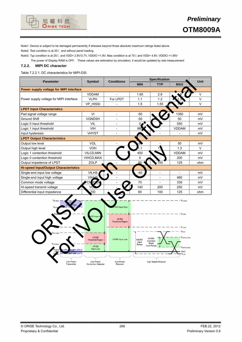
PPrreelliimmiinnaarryy
OTM8009A
© ORISE Technology Co., Ltd.
Proprietary & Confidential
268 FEB.22, 2012
Preliminary Version 0.8
Note1. Device is subject to be damaged permanently if stresses beyond those absolute maximum ratings listed above.
Note2. Test condition is at 25 and without panel loading.
Note3. Typ condition is at 25 and VDD= 2.8V/3.7V, VDDIO =1.8V; Max condition is at 70 and VDD= 4.8V, VDDIO =1.95V
The power of Display RAM is OFF. These values are estimation by simulation, it would be updated by real measurement
7.2.2. MIPI DC character
Table 7.2.2.1: DC characteristics for MIPI-DSI
Specification Parameter Symbol Conditions
MIN TYP MAX Unit
Power supply voltage for MIPI Interface
VDDAM - 1.65 2.8 4.8 V
VLPH For LPDT 1.1 1.2 1.3 V Power supply voltage for MIPI interface
VP_HISSI - 1.5 1.55 1.6 V
LPDT Input Characteristics
Pad signal voltage range VI - -50 - 1350 mV
Ground Shift VGNDSH - -50 - 50 mV
Logic 0 input threshold VIL - 0 - 550 mV
Logic 1 input threshold VIH - 880 - VDDAM mV
Input hysteresis VHYST - 25 - - mV
LPDT Output Characteristics
Output low level VOL - -50 - 50 mV
Output high level VOH - 1.1 1.2 1.3 V
Logic 1 contention threshold VILCD,MIN - 450 - VDDAM mV
Logic 0 contention threshold VIHCD,MAX - 0 - 200 mV
Output impedence of LPDT ZOLP - 80 100 125 ohm
Hi-speed Input/Output Characteristics
Single-end input low voltage VILHS - -40 - - mV
Single-end input high voltage VIHHS - - - 460 mV
Common mode voltage VCMRXDC - 70 - 330 mV
Hi-speed transmit voltage VOD - 140 200 250 mV
Differential input impedence ZID - 80 100 125 ohm
ORISE Tec
h Con
fiden
tial
For IV
O Use
Only

PPrreelliimmiinnaarryy
OTM8009A
© ORISE Technology Co., Ltd.
Proprietary & Confidential
269 FEB.22, 2012
Preliminary Version 0.8
7.2.3. MDDI DC character
Table 7.2.3.1: DC characteristics for MDDI
7.3. AC timing characteristics
7.3.1. MIPI-DSI characteristics
7.3.1.1. High speed mode
DSI-CLK+
DSI-CLK-
DSI-Dn+
DSI-Dn-
tDS tDStDH tDH
Specification Parameter Symbol Conditions
MIN TYP MAX Unit
Power supply voltage for MDDI interface VDDAM - 1.65 2.8 4.8 V
Data input high level voltage VIT+off - 100 125 mV
Data input low level voltage VIT-off 75 100 - mV
Data/Strobe input high level voltage VIT+ VT=0V - 0 50 mV
Data/Strobe input low level voltage VIT- VT=0V -50 0 - mV
Current consumption in Hibemation Ihib VDDAM=2.8V ; 550Mbps - 40 - uA
Current consumption in Data transfer Itrans VDDAM=2.8V ; 550Mbps - 4 - mA
Differential input impedence Zt - 80 100 125 Ohm
Specification Parameter Symbol Parameter
MIN TYP MAX Unit
High Speed mode
DSI-CLK+/- 2xUIINST Double UI instantaneous 4 - 25 ns DSI-CLK+/- UIINSTA , UIINSTB UI instantaneous Halfs 2 - 12.5 ns
DSI-Dn+/- tDS Data to clock setup time 0.15 - - UI
DSI-Dn+/- tDH Data to clock hold time 0.15 - - UI
DSI-CLK+/- tDRTCLK Differential rise time for clock 150 - 0.3UI ps
DSI-Dn+/- tDRTDATA Differential rise time for data 150 - 0.3UI ps
DSI-CLK+/- tDFTCLK Differential fall time for clock 150 - 0.3UI ps
DSI-Dn+/- tDFTDATA Differential fall time for data 150 - 0.3UI ps
ORISE Tec
h Con
fiden
tial
For IV
O Use
Only
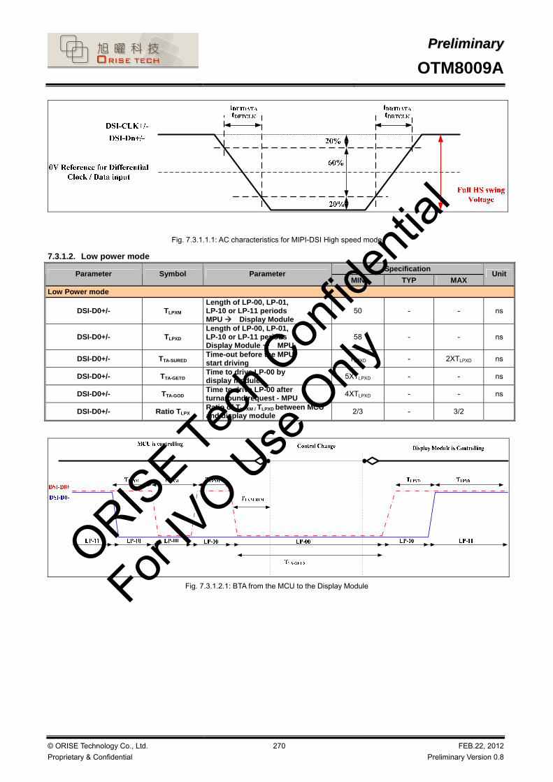
PPrreelliimmiinnaarryy
OTM8009A
© ORISE Technology Co., Ltd.
Proprietary & Confidential
270 FEB.22, 2012
Preliminary Version 0.8
Fig. 7.3.1.1.1: AC characteristics for MIPI-DSI High speed mode
7.3.1.2. Low power mode
Fig. 7.3.1.2.1: BTA from the MCU to the Display Module
Specification Parameter Symbol Parameter
MIN TYP MAX Unit
Low Power mode
DSI-D0+/- TLPXM Length of LP-00, LP-01, LP-10 or LP-11 periods MPU Display Module
50 - - ns
DSI-D0+/- TLPXD Length of LP-00, LP-01, LP-10 or LP-11 periods Display Module MPU
58 - - ns
DSI-D0+/- TTA-SURED Time-out before the MPU start driving TLPXD - 2XTLPXD ns
DSI-D0+/- TTA-GETD Time to drive LP-00 by display module 5XTLPXD - - ns
DSI-D0+/- TTA-GOD Time to drive LP-00 after turnaround request - MPU 4XTLPXD - - ns
DSI-D0+/- Ratio TLPX Ratio of TLPXM / TLPXD between MCU and display module
2/3 - 3/2
ORISE Tec
h Con
fiden
tial
For IV
O Use
Only

PPrreelliimmiinnaarryy
OTM8009A
© ORISE Technology Co., Ltd.
Proprietary & Confidential
271 FEB.22, 2012
Preliminary Version 0.8
Fig. 7.3.1.2.2: BTA from the Display Module to the MCU
7.3.1.3. Bursts
Fig. 7.3.1.3.1: High Speed Data Transmission Bursts
Specification Parameter Symbol Parameter
MIN TYP MAX Unit
High Speed Data Transmission Bursts
DSI-Dn+/- TLPX Length of any low-power state period 50 - - ns
DSI-Dn+/- THS-PREPARE Time to drive LP-00 to prepare for HS transmission 40ns + 4UI - 85ns + 6UI ns
DSI-Dn+/- THS-PREPARE
+THS-ZERO THS-PREPARE + time to drive HS-0 before the sync sequence
145ns + 10UI - - ns
DSI-Dn+/- TD-TERM-EN Time to enable Data Lane receiver line termination measured from when Dn crosses VIL(max)
Time for Dn to reach
VTERM-EN - 35ns + 4UI ns
DSI-Dn+/- THS-SKIP Time-out at RX to ignore transition period of EoT 40 - 55ns + 4UI ns
DSI-Dn+/- THS-TRAIL Time to drive flipped differential state after last payload data bit of a HS transmission burst
max (8UI, 60ns+4UI)
- - ns
DSI-Dn+/- THS-EXIT Time to drive LP-11 after HS burst 100 - - ns
DSI-Dn+/- TEoT Time from start of THS-TRAIL period to start of LP-11 state
- - 105ns + 12UI ns
ORISE Tec
h Con
fiden
tial
For IV
O Use
Only

PPrreelliimmiinnaarryy
OTM8009A
© ORISE Technology Co., Ltd.
Proprietary & Confidential
272 FEB.22, 2012
Preliminary Version 0.8
Fig. 7.3.1.3.2: Switching the clock Lane between clock Transmission and Low Power Mode
Specification Parameter Symbol Parameter
MIN TYP MAX Unit
Switching the clock Lane between clock Transmission and Low Power Mode
DSI-CLK+/- TCLK-POST
Time that the transmitter shall continue sending HS clock after the last associated Data Lane has transitioned to LP mode
60ns + 52UI - - ns
DSI-CLK+/- TCLK-PRE
Time that the HS clock shall be driven prior to any associated Data Lane beginning the transition from LP to HS mode
8 - - UI
DSI-CLK+/- TCLK-PREPARE Time to drive LP-00 to prepare for HS clock transmission
38 - 95 ns
DSI-CLK+/- TCLK-TERM-EN
Time to enable Clock Lane receiver line termination measured from when Dn crosses VIL(max)
Time for Dn to reach
VTERM-EN - 38 ns
DSI-CLK+/- TCLK-PREPARE
+TCLK-ZERO TCLK-PREPARE + time for lead HS-0 drive period before starting Clock
300 - - ns
DSI-CLK+/- TCLK-TRAIL Time to drive HS differential state after last payload clock bit of a HS transmission burst
60 - - ns
DSI-CLK+/- TEoT Time from start of TCLK-TRAIL period to start of LP-11 state
- - 105ns + 12UI ns
ORISE Tec
h Con
fiden
tial
For IV
O Use
Only

PPrreelliimmiinnaarryy
OTM8009A
© ORISE Technology Co., Ltd.
Proprietary & Confidential
273 FEB.22, 2012
Preliminary Version 0.8
7.3.1.4. LP-11 between high speed and low power modes
DSI-D0 High Speed or Low Power modes are starting or finishing from/to Stop State (SS, LP-11) when 4
different combinations, what are listed below, are possible:
1. High Speed Mode => Stop State (SS, LP-11) => High Speed Mode
2. High Speed Mode => Stop State (SS, LP-11) => Low Power Mode
3. Low Power Mode => Stop State (SS, LP-11) => High Speed Mode
4. Low Power Mode => Stop State (SS, LP-11) => Low Power Mode
The Low Power Mode is also including 2 different functions:
1. Escape
2. Bus Turnaround (BTA)
Stop State (SS, LP-11) Timings from Previous mode to Next mode
Previous Next
LP11
Escape mode
HSDT
BTA
Escape mode HSDT BTA
Previous
Next
100 ns
Min Max Min Max Min Max
- 100 ns - 100 ns -
60ns + 52UI - 60ns + 52UI - 60ns + 52UI -
100 ns - 100 ns - 100 ns -
ORISE Tec
h Con
fiden
tial
For IV
O Use
Only

PPrreelliimmiinnaarryy
OTM8009A
© ORISE Technology Co., Ltd.
Proprietary & Confidential
274 FEB.22, 2012
Preliminary Version 0.8
7.3.2. MDDI AC timing characteristics
Table 7.3.2.1: AC characteristics for MDDI
7.3.3. Allel Interface Characteristics 24/16/8-bits bus (8080-series MCU)
Specification Parameter Symbol Conditions
MIN TYP MAX Unit
Data Transfer Speed 1/tBIT - 384 550 MbpsTransfer input skew |Tskew_Pair| - - 50 ps
Data _Stb input skew |Tskew_Data|
VCI=2.3V~5.5V VDDIO=1.65~3.6V
TA=-30~+70 - - 300 ps
D/CX
CSX
TAST
VIH
VIL
TAHT
VIH
VIL
TRC/TRCFM
TRDL/TRDLFM
TRDH/ TRDHFM
TAST
TRCS/TRCSFM TAHT
WRX
D[23:0] Write
RDX
D[23:0] Read
VIH
VIL
TODHTRAT/ TRATFM
Fig. 7.3.3.1 Parallel interface characteristics (8080-Series MCU)
VIH
VIL
TDST TDHT
TWC
TWRL TWRH
VIH
VIL
TCS TCSF
TCHW
VIH
VIL TCSF
TCSH
TCHW
ORISE Tec
h Con
fiden
tial
For IV
O Use
Only

PPrreelliimmiinnaarryy
OTM8009A
© ORISE Technology Co., Ltd.
Proprietary & Confidential
275 FEB.22, 2012
Preliminary Version 0.8
Table 7.3.3.1: AC characteristics for parallel interface 24/18/16/8-bits bus (8080-series MCU)
Signal Symbol Parameter MIN MAX Unit Description
TAST Address setup time 0 nsD/CX
TAHT Address hold time (Write/Read) 10 ns-
TCHW Chip select “H” pulse width 0 ns
TCS Chip select setup time (Write) 15 ns
TRCS Chip select setup time (Read ID) 45 ns
TRCSFM Chip select setup time (Read FM) 355 ns
TCSF Chip select wait time (Write/Read) 10 ns
CSX
TCSH Chip select hold time 10 ns
-(3-transfer for one pixel) -(1-transfer for one pixel)
TWC Write cycle 66 ns
TWRH Control pulse “H” duration 15 nsWRX
TWRL Control pulse “L” duration 15 ns
TRC Read cycle (ID) 160 ns
TRDH Control pulse “H” duration (ID) 90 nsRDX (ID)
TRDL Control pulse “L” duration (ID) 45 ns
When read ID1~ID3 data
TRCFM Read cycle (FM = Frame Memory) 450 ns
TRDHFM Control pulse “H” duration (FM) 90 nsRDX (FM)
TRDLFM Control pulse “L” duration (FM) 355 ns
When read from frame memory
TDST Data setup time 10 ns
TDHT Data hold time 10 ns
TRAT Read access time (ID) 40 ns
TRATFM Read access time (FM) 340 ns
D[23:0]
TODH Output disable time 20 80 ns
For maximum CL=30pF For minimum CL=8pF
Note 1: VDDIO=1.65 to 3.6V, VCI=2.3 to 5.5V, VSSA=VSS=0V, Ta=-30 to 70
Note 2: The input signal rise time and fall time (Tr, Tf) is specified at 15 ns or less. Logic high and low levels are specified as 30% and 70% of VDDIO for Input signals.
ORISE Tec
h Con
fiden
tial
For IV
O Use
Only

PPrreelliimmiinnaarryy
OTM8009A
© ORISE Technology Co., Ltd.
Proprietary & Confidential
276 FEB.22, 2012
Preliminary Version 0.8
VIH
VIL
VIH
VIL
CSX
WRX
RDX
TWRH
VIH
VILTWRH /TRDHFM
Fig. 7.3.3.4 Write to read and Read to write timing
CSX
WRX RDX
Fig. 7.3.3.3 Chip selection (CSX) timing
TCSF Min. 5ns
VIH
VIL
TCHW
VIH
VIL
VIH=0.7*VDDIO
VIL=0.3*VDDIO
TR TF
Input Signal Slope
TR=TF<= 15ns
VOH=0.8*VDDIO
VOL=0.2*VDDIO
TR TF
Output Signal Slope
TR=TF<= 15ns
Fig. 7.3.3.2 Rising and Falling timing for Input and Output signal
ORISE Tec
h Con
fiden
tial
For IV
O Use
Only

PPrreelliimmiinnaarryy
OTM8009A
© ORISE Technology Co., Ltd.
Proprietary & Confidential
277 FEB.22, 2012
Preliminary Version 0.8
7.3.4. Serial interface characteristics (SPI)
Table 7.3.4.1 SPI Interface Characteristics
Signal Symbol Parameter MIN MAX Unit Description
TCSS Chip select setup time 15 - ns
TCSH Chip select hold time 15 - ns
TSCC Chip select setup time 20 - ns CSX
TCHW Chip select setup time 40 - ns
TSCYCW Serial clock cycle (Write) 66 - ns
TSHW SCL “H” pulse width (Write) 10 - ns
TSLW SCL “L” pulse width (Write) 10 - ns
-
TSCYCR Serial clock cycle (Read) 150 - ns
TSHR SCL “H” pulse width (Read) 60 - ns
SCL
TSLR SCL “L” pulse width (Read) 60 - ns
TSDS Data setup time 10 - ns
TSDH Data hold time 10 - ns
TACC Access time 10 50 ns
SDA (DIN)
(DOUT) TOH Output disable time 15 50 ns
For maximum CL=30pF For minimum CL=8pF
Note 1: VDDIO=1.65 to 3.6V, VCI=2.3 to 5.5V, VSSA=VSS=0V, Ta=-30 to 70
Note 2: The input signal rise time and fall time (tr, tf) is specified at 15 ns or less. Logic high and low levels are specified as 30% and 70% of VDDIO for Input signals.
CSX
TCSS
TCHW VIH
VIL
TCSH
TSCCVIH
VIL SCL
TSCYCW /TSCYCR
TSLW /TSLR
TSHW /TSHR
VIH
VIL
TSDS TSDH
VIH
VIL
TACC TOH
SDI (DIN)
SDO (DOUT)
Figure 7.3.4.1 3-pin Serial Interface Characteristics
ORISE Tec
h Con
fiden
tial
For IV
O Use
Only

PPrreelliimmiinnaarryy
OTM8009A
© ORISE Technology Co., Ltd.
Proprietary & Confidential
278 FEB.22, 2012
Preliminary Version 0.8
7.3.5. RGB interface characteristics
Table 7.3.5.1 RGB Interface Characteristics
(VCI=2.3V~5.5V, VDDIO = 1.65V~3.6V, Ta = -40 ~ 85)
Signal Symbol Parameter MIN MAX Unit Description
VSST VS setup time 5 - ns Vsync
VSHT VS hold time 5 - ns
HSST HS setup time 5 - ns Hsync
HSHT HS hold time 5 - ns
Pixel clock duty cycle 33 67 %
PCLKLT Pixel clock low duration 14 - ns PCLK
PCLKHT Pixel clock high duration 14 - ns
DST Data setup time 5 - ns D [23:0], DE
DHT Date hold time 5 - ns
Vsync
Hsync
PCLK
D[23:0],DE
Figure 7.3.5.1 AC Timing Characteristics, RGB Interface
ORISE Tec
h Con
fiden
tial
For IV
O Use
Only

PPrreelliimmiinnaarryy
OTM8009A
© ORISE Technology Co., Ltd.
Proprietary & Confidential
279 FEB.22, 2012
Preliminary Version 0.8
7.3.6. I2C interface characteristics
SDA
SCL
tBUF
tHD;STA
tLOW
tHD;DATA
tHIGH
tSU;DATA
Table 7.3.6.1 I2C Interface Characteristics
Symbol Parameter Conditions Min. Typ. Max. Unit
fSCLK SCL clock frequency DC - 400 KHz
tLOW SCL clock LOW period 1.3 - - s
tHIGH SCL clock HIGH period 0.6 - - s
tSU;DATA data set-up time 100 - - ns
tHD;DATA data hold time 0 - 0.9 s
tR SCL and SDA rise time Note 2
20+0.1Cb - 300 ns
tF SCL and SDA fall time Note 2
20+0.1Cb - 300 ns
tF SDA fall time for read out 20+0.1Cb - 1000 ns
Cb Capacitive load represented by each bus line - - 400 pF
tSU;STA Setup time for a repeated START condition 0.6 - - s
tHD;STA START condition hold time 0.6 - - s
tSU;STO Setup time for STOP condition 0.6 - - s
tSW Tolerable spike width on bus Note 1
- - 50 ns
tBUF BUS free time between a STOP and START condition 1.3 - - s
Note1: The device inputs SDA and SCL are filtered and will reject spikes on the bus lines of width <tSW(max) .
Note2: The rise and fall times specified here refer to the driver device and are part of the general fast I2C-bus specification. Cb = capacitive load per bus line.
Note3: All timing values are valid within the operating supply voltage and ambient temperature ranges and are referenced to VIL and VIH with an input voltage
swing of VSS to VDDIO.
ORISE Tec
h Con
fiden
tial
For IV
O Use
Only

PPrreelliimmiinnaarryy
OTM8009A
© ORISE Technology Co., Ltd.
Proprietary & Confidential
280 FEB.22, 2012
Preliminary Version 0.8
7.3.7. Reset timing characteristics
Table 7.3.7.1 Reset input timing VSS=0V, VDDIO=1.6V to 3.6V, VCI=2.5V to 5.5V,Ta = -30 to 70C
Symbol Parameter Related Pins MIN TYP MAX Note Unit
tRESW *1) Reset low pulse width RESX 10 - - - s
- - - 5 When reset applied during
Sleep in mode ms
tREST *2) Reset complete time - - 120
When reset applied during Sleep out mode
ms
Note 1. Spike due to an electrostatic discharge on RESX line does not cause irregular system reset according to the table below.
RESX Pulse Action
Shorter than 5s Reset Rejected
Longer than 10s Reset
Between 5s and 10s Reset starts
(It depends on voltage and temperature condition.)
Note 2. During the resetting period, the display will be blanked (The display is entering blanking sequence, which maximum time is 120 ms, when Reset Starts
in Sleep Out –mode. The display remains the blank state in Sleep In –mode) and then return to Default condition for H/W reset.
Note 3. During Reset Complete Time, ID1/ID2/ID3/ID4 and VCOM value in OTP will be latched to internal register during this period. This loading is done every
time when there is H/W reset complete time (tREST) within 5ms after a rising edge of RESX.
Note 4. Spike Rejection also applies during a valid reset pulse as shown below:
Note 5. It is necessary to wait 5msec after releasing RESX before sending commands. Also Sleep Out command cannot be sent for
120msec.
10s
10s
Reset is accepted
Internal Status
!RES
tRESW
tREST
Resetting Initial Condition (Default for H/W reset)
Shorter than 5s
Normal Operation
RESX
ORISE Tec
h Con
fiden
tial
For IV
O Use
Only

PPrreelliimmiinnaarryy
OTM8009A
© ORISE Technology Co., Ltd.
Proprietary & Confidential
281 FEB.22, 2012
Preliminary Version 0.8
8. CHIP INFORMATION
8.1. PAD Assignment
Note1:Chip size included scribe line.
Note2:Have no temperature compensation design.
Symbol Size Symbol Size
A1 55 B6 40
A2 150 B7 60
A3 14 C1 42
B1 120 C2 13
B2 55 C3 28
B3 80 C4 30
B4 100 C5 55
B5 60 C6 115
Unit: um
8.2. PAD Dimension
Size Item PAD No.
X Y Unit
Chip Size - 24000 1380
Chip thickness -
250 ± 10(OTM8009A-C)
250 ± 10(OTM8009A-C1)
200 ± 10(OTM8009A-C2)
200 ± 10(OTM8009A-C3)
250 ± 10(OTM8009A-C4)
200 ± 10(OTM8009A-C5)
200 ± 10(OTM8009A-C6)
250 ± 10(OTM8009A-C7)
2 ~ 395 60 -- Pad pitch
398 ~ 2074 28 --
2 ~395 40 120
398 ~2074 13 115
1, 396 100 120 Pad size
397, 2075 42 115
um
Note1: Chip size included scribe line.
ORISE Tec
h Con
fiden
tial
For IV
O Use
Only

PPrreelliimmiinnaarryy
OTM8009A
© ORISE Technology Co., Ltd.
Proprietary & Confidential
282 FEB.22, 2012
Preliminary Version 0.8
8.3. Pad Location
NO. PAD NAME X-axis Y-axis
1 VSS -11880 -575 2 VSS -11790 -575 3 PADA1 -11730 -575 4 PADB1 -11670 -575 5 VCOM -11610 -575 6 VCOM -11550 -575 7 VCOM -11490 -575 8 VCOM -11430 -575 9 VCOM -11370 -575 10 CONTACT1A -11310 -575 11 CONTACT1B -11250 -575 12 MTP_PWR -11190 -575 13 MTP_PWR -11130 -575 14 MTP_PWR -11070 -575 15 MTP_PWR -11010 -575 16 MTP_PWR -10950 -575 17 VGL -10890 -575 18 VGL -10830 -575 19 VGL -10770 -575 20 VGL -10710 -575 21 VGL_REG1 -10650 -575 22 VGL_REG1 -10590 -575 23 VRGH -10530 -575 24 VRGH -10470 -575 25 VCL -10410 -575 26 VCL -10350 -575 27 VCL -10290 -575 28 VCL -10230 -575 29 VREF_PWR -10170 -575 30 VREF_PWR -10110 -575 31 VREF_PWR -10050 -575 32 VREF_PWR -9990 -575 33 VSSA -9930 -575 34 VSSA -9870 -575 35 VSSA -9810 -575 36 VSSA -9750 -575 37 VDD -9690 -575 38 VDD -9630 -575 39 VDD -9570 -575 40 VDD -9510 -575 41 VDD -9450 -575 42 VDD -9390 -575 43 VDD -9330 -575 44 VDD -9270 -575 45 VSS -9210 -575 46 VSS -9150 -575 47 VSS -9090 -575 48 VSS -9030 -575 49 TEST0 -8970 -575 50 TEST1 -8910 -575 51 TEST2 -8850 -575 52 TEST3 -8790 -575 53 VDD -8730 -575 54 DIOPWR -8670 -575 55 DIOPWR -8610 -575
NO. PAD NAME X-axis Y-axis
56 VGSN -8550 -575
57 VGSN -8490 -575
58 VGSP -8430 -575
59 VGMN -8370 -575
60 VGMN -8310 -575
61 VGMP -8250 -575
62 VSS -8190 -575
63 VSS -8130 -575
64 VSS -8070 -575
65 VDD_18V -8010 -575
66 VDD_18V -7950 -575
67 VDD_18V -7890 -575
68 VDD -7830 -575
69 VDD -7770 -575
70 VDD -7710 -575
71 VCL -7650 -575
72 VCL -7590 -575
73 VCL -7530 -575
74 VCL -7470 -575
75 VCL -7410 -575
76 VCL -7350 -575
77 VSSA -7290 -575
78 VSSA -7230 -575
79 VSSA -7170 -575
80 VDDIO -7110 -575
81 LANSEL -7050 -575
82 DSWAP -6990 -575
83 PSWAP -6930 -575
84 VSS -6870 -575
85 DSTB_SEL -6810 -575
86 NBWSEL -6750 -575
87 VGSW3 -6690 -575
88 VGSW2 -6630 -575
89 VGSW1 -6570 -575
90 VGSW0 -6510 -575
91 VDDIO -6450 -575
92 I2C_SA1 -6390 -575
93 I2C_SA2 -6330 -575
94 IM3 -6270 -575
95 IM2 -6210 -575
96 IM1 -6150 -575
97 IM0 -6090 -575
98 GPO3 -6030 -575
99 GPO2 -5970 -575
100 GPO1 -5910 -575
101 GPO0 -5850 -575
102 EXB1T -5790 -575
103 TE_L -5730 -575
104 VSEL -5670 -575
105 SDO -5610 -575
106 SDI -5550 -575
107 DCX -5490 -575
108 WRX -5430 -575
109 RDX -5370 -575
110 CSX -5310 -575
NO. PAD NAME X-axis Y-axis
111 RESX -5250 -575
112 VSS -5190 -575
113 VSS -5130 -575
114 VSS -5070 -575
115 VDDIO -5010 -575
116 VDDIO -4950 -575
117 VDDIO -4890 -575
118 D23 -4830 -575
119 D22 -4770 -575
120 D21 -4710 -575
121 D20 -4650 -575
122 D19 -4590 -575
123 D18 -4530 -575
124 D17 -4470 -575
125 D16 -4410 -575
126 D15 -4350 -575
127 D14 -4290 -575
128 D13 -4230 -575
129 D12 -4170 -575
130 D11 -4110 -575
131 D10 -4050 -575
132 D9 -3990 -575
133 D8 -3930 -575
134 D7 -3870 -575
135 D6 -3810 -575
136 D5 -3750 -575
137 D4 -3690 -575
138 D3 -3630 -575
139 D2 -3570 -575
140 D1 -3510 -575
141 D0 -3450 -575
142 DE -3390 -575
143 PCLK -3330 -575
144 HS -3270 -575
145 VS -3210 -575
146 LEDPWM -3150 -575
147 LEDON -3090 -575
148 KBBC -3030 -575
149 ERR -2970 -575
150 VDDIO -2910 -575
151 VDDIO -2850 -575
152 VDDIO -2790 -575
153 VSS -2730 -575
154 VSS -2670 -575
155 VSS -2610 -575
156 VDDA -2550 -575
157 VDDA -2490 -575
158 VDDA -2430 -575
159 VDDA -2370 -575
160 VSSA -2310 -575
161 VSSA -2250 -575
162 VSSA -2190 -575
163 VSSA -2130 -575
164 NVDDA -2070 -575
165 NVDDA -2010 -575
ORISE Tec
h Con
fiden
tial
For IV
O Use
Only

PPrreelliimmiinnaarryy
OTM8009A
© ORISE Technology Co., Ltd.
Proprietary & Confidential
283 FEB.22, 2012
Preliminary Version 0.8
NO. PAD NAME X-axis Y-axis
166 NVDDA -1950 -575 167 NVDDA -1890 -575 168 NVDDA -1830 -575 169 VCC -1770 -575 170 VCC -1710 -575 171 VCC -1650 -575 172 VCC -1590 -575 173 VSS -1530 -575 174 VSS -1470 -575 175 VSS -1410 -575 176 VSS -1350 -575 177 VDD_18V -1290 -575 178 VDD_18V -1230 -575 179 VDD_18V -1170 -575 180 VDD_18V -1110 -575 181 VSS -1050 -575 182 VSS -990 -575 183 VSS -930 -575 184 VSS -870 -575 185 VSS -810 -575 186 D1_P -750 -575 187 D1_P -690 -575 188 D1_P -630 -575 189 D1_P -570 -575 190 D1_N -510 -575 191 D1_N -450 -575 192 D1_N -390 -575 193 D1_N -330 -575 194 LVDSVSS -270 -575 195 LVDSVSS -210 -575 196 CLK_P -150 -575 197 CLK_P -90 -575 198 CLK_P -30 -575 199 CLK_P 30 -575 200 CLK_N 90 -575 201 CLK_N 150 -575 202 CLK_N 210 -575 203 CLK_N 270 -575 204 LVDSVSS 330 -575 205 LVDSVSS 390 -575 206 D0_P 450 -575 207 D0_P 510 -575 208 D0_P 570 -575 209 D0_P 630 -575 210 D0_N 690 -575 211 D0_N 750 -575 212 D0_N 810 -575 213 D0_N 870 -575 214 LVDSVSS 930 -575 215 LVDSVSS 990 -575 216 VDDP 1050 -575 217 VDDP 1110 -575 218 VDDP 1170 -575 219 LVDSVDD 1230 -575 220 LVDSVDD 1290 -575 221 LVDSVDD 1350 -575 222 VDDAM 1410 -575
NO. PAD NAME X-axis Y-axis
223 VDDAM 1470 -575
224 VDDAM 1530 -575
225 VDDAM 1590 -575
226 VDDAM 1650 -575
227 VDD 1710 -575
228 VDD 1770 -575
229 VDD 1830 -575
230 OSC_TEST 1890 -575
231 TE_R 1950 -575
232 VSS 2010 -575
233 VSS 2070 -575
234 VSS 2130 -575
235 VSS 2190 -575
236 VREFCP 2250 -575
237 VREFCP 2310 -575
238 VRGH_DMY 2370 -575
239 VRGH_DMY 2430 -575
240 EXTP 2490 -575
241 EXTP 2550 -575
242 CSP 2610 -575
243 CSP 2670 -575
244 EXTN 2730 -575
245 EXTN 2790 -575
246 CSN 2850 -575
247 CSN 2910 -575
248 VDD 2970 -575
249 VDD 3030 -575
250 VDD 3090 -575
251 VDD 3150 -575
252 VDD 3210 -575
253 VDD 3270 -575
254 VSS 3330 -575
255 VSS 3390 -575
256 VSS 3450 -575
257 VSS 3510 -575
258 VSS 3570 -575
259 VSS 3630 -575
260 C11P 3690 -575
261 C11P 3750 -575
262 C11P 3810 -575
263 C11N 3870 -575
264 C11N 3930 -575
265 C11N 3990 -575
266 C12P 4050 -575
267 C12P 4110 -575
268 C12P 4170 -575
269 C12N 4230 -575
270 C12N 4290 -575
271 C12N 4350 -575
272 C13P 4410 -575
273 C13P 4470 -575
274 C13P 4530 -575
275 C13N 4590 -575
276 C13N 4650 -575
277 C13N 4710 -575
278 C14P 4770 -575
279 C14P 4830 -575
NO. PAD NAME X-axis Y-axis
280 C14P 4890 -575
281 C14N 4950 -575
282 C14N 5010 -575
283 C14N 5070 -575
284 VDDA 5130 -575
285 VDDA 5190 -575
286 VDDA 5250 -575
287 VDDA 5310 -575
288 VSS 5370 -575
289 VSS 5430 -575
290 VSSA 5490 -575
291 VSSA 5550 -575
292 VSSA 5610 -575
293 NVDDA 5670 -575
294 NVDDA 5730 -575
295 NVDDA 5790 -575
296 NVDDA 5850 -575
297 NVDDA 5910 -575
298 NVDDA 5970 -575
299 C21P 6030 -575
300 C21P 6090 -575
301 C21P 6150 -575
302 C21N 6210 -575
303 C21N 6270 -575
304 C21N 6330 -575
305 C22P 6390 -575
306 C22P 6450 -575
307 C22P 6510 -575
308 C22N 6570 -575
309 C22N 6630 -575
310 C22N 6690 -575
311 C23P 6750 -575
312 C23P 6810 -575
313 C23P 6870 -575
314 C23N 6930 -575
315 C23N 6990 -575
316 C23N 7050 -575
317 C24P 7110 -575
318 C24P 7170 -575
319 C24P 7230 -575
320 C24N 7290 -575
321 C24N 7350 -575
322 C24N 7410 -575
323 VDD 7470 -575
324 VDD 7530 -575
325 VDD 7590 -575
326 VDD 7650 -575
327 VDD 7710 -575
328 VCL 7770 -575
329 VCL 7830 -575
330 VCL 7890 -575
331 VCL 7950 -575
332 VCL 8010 -575
333 VCL 8070 -575
334 VCL 8130 -575
335 VSSA 8190 -575
336 VSSA 8250 -575
ORISE Tec
h Con
fiden
tial
For IV
O Use
Only

PPrreelliimmiinnaarryy
OTM8009A
© ORISE Technology Co., Ltd.
Proprietary & Confidential
284 FEB.22, 2012
Preliminary Version 0.8
NO. PAD NAME X-axis Y-axis
337 VSSA 8310 -575 338 VSS 8370 -575 339 VSS 8430 -575 340 VSS 8490 -575 341 VSS 8550 -575 342 C31P 8610 -575 343 C31P 8670 -575 344 C31P 8730 -575 345 C31N 8790 -575 346 C31N 8850 -575 347 C31N 8910 -575 348 C32P 8970 -575 349 C32P 9030 -575 350 C32P 9090 -575 351 C32N 9150 -575 352 C32N 9210 -575 353 C32N 9270 -575 354 VDD_18V 9330 -575 355 VDD_18V 9390 -575 356 VDD_18V 9450 -575 357 VSS 9510 -575 358 VSS 9570 -575 359 VSS 9630 -575 360 C41P 9690 -575 361 C41P 9750 -575 362 C41N 9810 -575 363 C41N 9870 -575 364 VGH 9930 -575 365 VGH 9990 -575 366 VGHO_R 10050 -575 367 VGHO_R 10110 -575 368 VRGH 10170 -575 369 VRGH 10230 -575 370 C51P 10290 -575 371 C51P 10350 -575 372 C51N 10410 -575 373 C51N 10470 -575 374 VGL_REG 10530 -575 375 VGL_REG 10590 -575 376 VGL 10650 -575 377 VGL 10710 -575 378 VGL 10770 -575 379 VGL 10830 -575 380 VGL 10890 -575 381 VGL 10950 -575 382 TEST4 11010 -575 383 TEST5 11070 -575 384 TEST6 11130 -575 385 TEST7 11190 -575 386 CONTACT2A 11250 -575 387 CONTACT2B 11310 -575 388 VCOM 11370 -575 389 VCOM 11430 -575 390 VCOM 11490 -575 391 VCOM 11550 -575 392 VCOM 11610 -575 393 PADA2 11670 -575
NO. PAD NAME X-axis Y-axis
394 PADB2 11730 -575
395 VSS 11790 -575
396 VSS 11880 -575
397 VSS 11760 577.5
398 VSS 11732 432.5
399 VSS 11718 577.5
400 PADA3 11704 432.5
401 PADB3 11690 577.5
402 VGHO_R 11676 432.5
403 VGHO_R 11662 577.5
404 VGHO_R 11648 432.5
405 VGL 11634 577.5
406 VGL 11620 432.5
407 VGL 11606 577.5
408 GDOUT1 11592 432.5
409 GDOUT1 11578 577.5
410 GDOUT2 11564 432.5
411 GDOUT2 11550 577.5
412 LVGL2 11536 432.5
413 LVGL2 11522 577.5
414 LVGL2 11508 432.5
415 VRGH 11494 577.5
416 VRGH 11480 432.5
417 VRGH 11466 577.5
418 VGL 11452 432.5
419 VGL 11438 577.5
420 VGL 11424 432.5
421 GDOUT3 11410 577.5
422 GDOUT3 11396 432.5
423 GDOUT4 11382 577.5
424 GDOUT4 11368 432.5
425 GDOUT5 11354 577.5
426 GDOUT5 11340 432.5
427 GDOUT6 11326 577.5
428 GDOUT6 11312 432.5
429 GDOUT7 11298 577.5
430 GDOUT7 11284 432.5
431 GDOUT8 11270 577.5
432 GDOUT8 11256 432.5
433 GDOUT9 11242 577.5
434 GDOUT9 11228 432.5
435 GDOUT10 11214 577.5
436 GDOUT10 11200 432.5
437 GDOUT11 11186 577.5
438 GDOUT11 11172 432.5
439 GDOUT12 11158 577.5
440 GDOUT12 11144 432.5
441 GDOUT13 11130 577.5
442 GDOUT13 11116 432.5
443 GDOUT14 11102 577.5
444 GDOUT14 11088 432.5
445 GDOUT15 11074 577.5
446 GDOUT15 11060 432.5
447 GDOUT16 11046 577.5
448 GDOUT16 11032 432.5
449 VGHO_R 11018 577.5
450 VGHO_R 11004 432.5
NO. PAD NAME X-axis Y-axis
451 VGHO_R 10990 577.5
452 VGHO_R 10976 432.5
453 VGHO_R 10962 577.5
454 VGHO_R 10948 432.5
455 VGHO_R 10934 577.5
456 VGHO_R 10920 432.5
457 VGL 10906 577.5
458 VGL 10892 432.5
459 VGL 10878 577.5
460 VGL 10864 432.5
461 VGL 10850 577.5
462 VGL 10836 432.5
463 VGL 10822 577.5
464 VGL 10808 432.5
465 VGL 10794 577.5
466 VSS 10780 432.5
467 VSS 10766 577.5
468 SDUM0 10752 432.5
469 SDUM1 10738 577.5
470 S1 10724 432.5
471 S2 10710 577.5
472 S3 10696 432.5
473 S4 10682 577.5
474 S5 10668 432.5
475 S6 10654 577.5
476 S7 10640 432.5
477 S8 10626 577.5
478 S9 10612 432.5
479 S10 10598 577.5
480 S11 10584 432.5
481 S12 10570 577.5
482 S13 10556 432.5
483 S14 10542 577.5
484 S15 10528 432.5
485 S16 10514 577.5
486 S17 10500 432.5
487 S18 10486 577.5
488 S19 10472 432.5
489 S20 10458 577.5
490 S21 10444 432.5
491 S22 10430 577.5
492 S23 10416 432.5
493 S24 10402 577.5
494 S25 10388 432.5
495 S26 10374 577.5
496 S27 10360 432.5
497 S28 10346 577.5
498 S29 10332 432.5
499 S30 10318 577.5
500 S31 10304 432.5
501 S32 10290 577.5
502 S33 10276 432.5
503 S34 10262 577.5
504 S35 10248 432.5
505 S36 10234 577.5
506 S37 10220 432.5
507 S38 10206 577.5
ORISE Tec
h Con
fiden
tial
For IV
O Use
Only

PPrreelliimmiinnaarryy
OTM8009A
© ORISE Technology Co., Ltd.
Proprietary & Confidential
285 FEB.22, 2012
Preliminary Version 0.8
NO. PAD NAME X-axis Y-axis
508 S39 10192 432.5 509 S40 10178 577.5 510 S41 10164 432.5 511 S42 10150 577.5 512 S43 10136 432.5 513 S44 10122 577.5 514 S45 10108 432.5 515 S46 10094 577.5 516 S47 10080 432.5 517 S48 10066 577.5 518 S49 10052 432.5 519 S50 10038 577.5 520 S51 10024 432.5 521 S52 10010 577.5 522 S53 9996 432.5 523 S54 9982 577.5 524 S55 9968 432.5 525 S56 9954 577.5 526 S57 9940 432.5 527 S58 9926 577.5 528 S59 9912 432.5 529 S60 9898 577.5 530 S61 9884 432.5 531 S62 9870 577.5 532 S63 9856 432.5 533 S64 9842 577.5 534 S65 9828 432.5 535 S66 9814 577.5 536 S67 9800 432.5 537 S68 9786 577.5 538 S69 9772 432.5 539 S70 9758 577.5 540 S71 9744 432.5 541 S72 9730 577.5 542 S73 9716 432.5 543 S74 9702 577.5 544 S75 9688 432.5 545 S76 9674 577.5 546 S77 9660 432.5 547 S78 9646 577.5 548 S79 9632 432.5 549 S80 9618 577.5 550 S81 9604 432.5 551 S82 9590 577.5 552 S83 9576 432.5 553 S84 9562 577.5 554 S85 9548 432.5 555 S86 9534 577.5 556 S87 9520 432.5 557 S88 9506 577.5 558 S89 9492 432.5 559 S90 9478 577.5 560 S91 9464 432.5 561 S92 9450 577.5 562 S93 9436 432.5 563 S94 9422 577.5 564 S95 9408 432.5
NO. PAD NAME X-axis Y-axis
565 S96 9394 577.5
566 S97 9380 432.5
567 S98 9366 577.5
568 S99 9352 432.5
569 S100 9338 577.5
570 S101 9324 432.5
571 S102 9310 577.5
572 S103 9296 432.5
573 S104 9282 577.5
574 S105 9268 432.5
575 S106 9254 577.5
576 S107 9240 432.5
577 S108 9226 577.5
578 S109 9212 432.5
579 S110 9198 577.5
580 S111 9184 432.5
581 S112 9170 577.5
582 S113 9156 432.5
583 S114 9142 577.5
584 S115 9128 432.5
585 S116 9114 577.5
586 S117 9100 432.5
587 S118 9086 577.5
588 S119 9072 432.5
589 S120 9058 577.5
590 S121 9044 432.5
591 S122 9030 577.5
592 S123 9016 432.5
593 S124 9002 577.5
594 S125 8988 432.5
595 S126 8974 577.5
596 S127 8960 432.5
597 S128 8946 577.5
598 S129 8932 432.5
599 S130 8918 577.5
600 S131 8904 432.5
601 S132 8890 577.5
602 S133 8876 432.5
603 S134 8862 577.5
604 S135 8848 432.5
605 S136 8834 577.5
606 S137 8820 432.5
607 S138 8806 577.5
608 S139 8792 432.5
609 S140 8778 577.5
610 S141 8764 432.5
611 S142 8750 577.5
612 S143 8736 432.5
613 S144 8722 577.5
614 S145 8708 432.5
615 S146 8694 577.5
616 S147 8680 432.5
617 S148 8666 577.5
618 S149 8652 432.5
619 S150 8638 577.5
620 S151 8624 432.5
621 S152 8610 577.5
NO. PAD NAME X-axis Y-axis
622 S153 8596 432.5
623 S154 8582 577.5
624 S155 8568 432.5
625 S156 8554 577.5
626 S157 8540 432.5
627 S158 8526 577.5
628 S159 8512 432.5
629 S160 8498 577.5
630 S161 8484 432.5
631 S162 8470 577.5
632 S163 8456 432.5
633 S164 8442 577.5
634 S165 8428 432.5
635 S166 8414 577.5
636 S167 8400 432.5
637 S168 8386 577.5
638 S169 8372 432.5
639 S170 8358 577.5
640 S171 8344 432.5
641 S172 8330 577.5
642 S173 8316 432.5
643 S174 8302 577.5
644 S175 8288 432.5
645 S176 8274 577.5
646 S177 8260 432.5
647 S178 8246 577.5
648 S179 8232 432.5
649 S180 8218 577.5
650 S181 8204 432.5
651 S182 8190 577.5
652 S183 8176 432.5
653 S184 8162 577.5
654 S185 8148 432.5
655 S186 8134 577.5
656 S187 8120 432.5
657 S188 8106 577.5
658 S189 8092 432.5
659 S190 8078 577.5
660 S191 8064 432.5
661 S192 8050 577.5
662 S193 8036 432.5
663 S194 8022 577.5
664 S195 8008 432.5
665 S196 7994 577.5
666 S197 7980 432.5
667 S198 7966 577.5
668 S199 7952 432.5
669 S200 7938 577.5
670 S201 7924 432.5
671 S202 7910 577.5
672 S203 7896 432.5
673 S204 7882 577.5
674 S205 7868 432.5
675 S206 7854 577.5
676 S207 7840 432.5
677 S208 7826 577.5
678 S209 7812 432.5
ORISE Tec
h Con
fiden
tial
For IV
O Use
Only
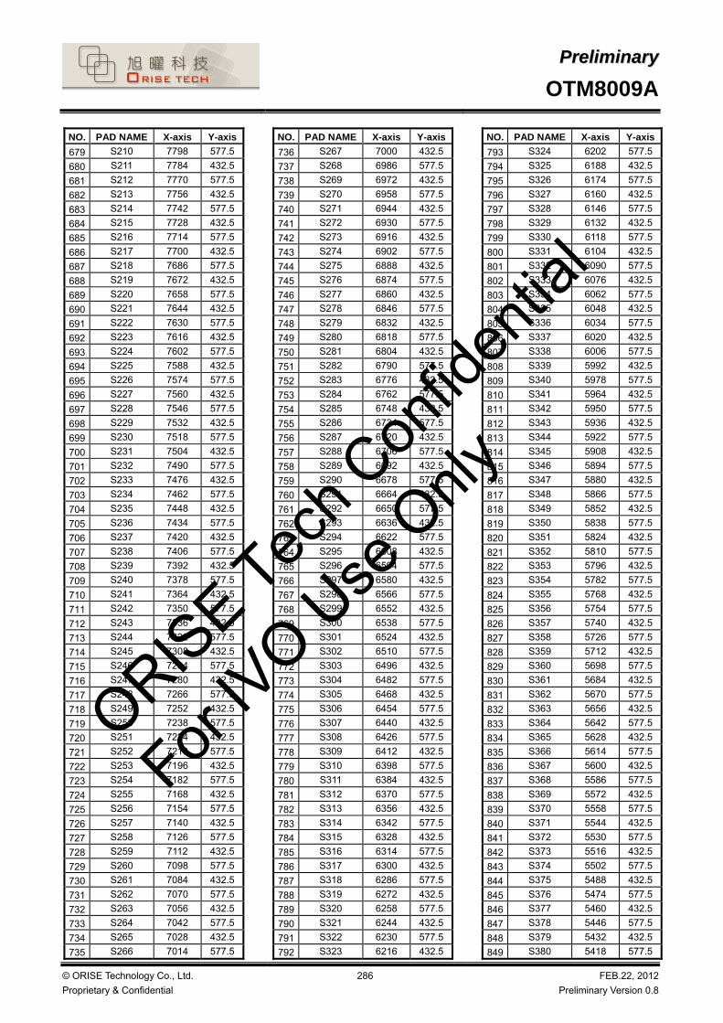
PPrreelliimmiinnaarryy
OTM8009A
© ORISE Technology Co., Ltd.
Proprietary & Confidential
286 FEB.22, 2012
Preliminary Version 0.8
NO. PAD NAME X-axis Y-axis
679 S210 7798 577.5 680 S211 7784 432.5 681 S212 7770 577.5 682 S213 7756 432.5 683 S214 7742 577.5 684 S215 7728 432.5 685 S216 7714 577.5 686 S217 7700 432.5 687 S218 7686 577.5 688 S219 7672 432.5 689 S220 7658 577.5 690 S221 7644 432.5 691 S222 7630 577.5 692 S223 7616 432.5 693 S224 7602 577.5 694 S225 7588 432.5 695 S226 7574 577.5 696 S227 7560 432.5 697 S228 7546 577.5 698 S229 7532 432.5 699 S230 7518 577.5 700 S231 7504 432.5 701 S232 7490 577.5 702 S233 7476 432.5 703 S234 7462 577.5 704 S235 7448 432.5 705 S236 7434 577.5 706 S237 7420 432.5 707 S238 7406 577.5 708 S239 7392 432.5 709 S240 7378 577.5 710 S241 7364 432.5 711 S242 7350 577.5 712 S243 7336 432.5 713 S244 7322 577.5 714 S245 7308 432.5 715 S246 7294 577.5 716 S247 7280 432.5 717 S248 7266 577.5 718 S249 7252 432.5 719 S250 7238 577.5 720 S251 7224 432.5 721 S252 7210 577.5 722 S253 7196 432.5 723 S254 7182 577.5 724 S255 7168 432.5 725 S256 7154 577.5 726 S257 7140 432.5 727 S258 7126 577.5 728 S259 7112 432.5 729 S260 7098 577.5 730 S261 7084 432.5 731 S262 7070 577.5 732 S263 7056 432.5 733 S264 7042 577.5 734 S265 7028 432.5 735 S266 7014 577.5
NO. PAD NAME X-axis Y-axis
736 S267 7000 432.5
737 S268 6986 577.5
738 S269 6972 432.5
739 S270 6958 577.5
740 S271 6944 432.5
741 S272 6930 577.5
742 S273 6916 432.5
743 S274 6902 577.5
744 S275 6888 432.5
745 S276 6874 577.5
746 S277 6860 432.5
747 S278 6846 577.5
748 S279 6832 432.5
749 S280 6818 577.5
750 S281 6804 432.5
751 S282 6790 577.5
752 S283 6776 432.5
753 S284 6762 577.5
754 S285 6748 432.5
755 S286 6734 577.5
756 S287 6720 432.5
757 S288 6706 577.5
758 S289 6692 432.5
759 S290 6678 577.5
760 S291 6664 432.5
761 S292 6650 577.5
762 S293 6636 432.5
763 S294 6622 577.5
764 S295 6608 432.5
765 S296 6594 577.5
766 S297 6580 432.5
767 S298 6566 577.5
768 S299 6552 432.5
769 S300 6538 577.5
770 S301 6524 432.5
771 S302 6510 577.5
772 S303 6496 432.5
773 S304 6482 577.5
774 S305 6468 432.5
775 S306 6454 577.5
776 S307 6440 432.5
777 S308 6426 577.5
778 S309 6412 432.5
779 S310 6398 577.5
780 S311 6384 432.5
781 S312 6370 577.5
782 S313 6356 432.5
783 S314 6342 577.5
784 S315 6328 432.5
785 S316 6314 577.5
786 S317 6300 432.5
787 S318 6286 577.5
788 S319 6272 432.5
789 S320 6258 577.5
790 S321 6244 432.5
791 S322 6230 577.5
792 S323 6216 432.5
NO. PAD NAME X-axis Y-axis
793 S324 6202 577.5
794 S325 6188 432.5
795 S326 6174 577.5
796 S327 6160 432.5
797 S328 6146 577.5
798 S329 6132 432.5
799 S330 6118 577.5
800 S331 6104 432.5
801 S332 6090 577.5
802 S333 6076 432.5
803 S334 6062 577.5
804 S335 6048 432.5
805 S336 6034 577.5
806 S337 6020 432.5
807 S338 6006 577.5
808 S339 5992 432.5
809 S340 5978 577.5
810 S341 5964 432.5
811 S342 5950 577.5
812 S343 5936 432.5
813 S344 5922 577.5
814 S345 5908 432.5
815 S346 5894 577.5
816 S347 5880 432.5
817 S348 5866 577.5
818 S349 5852 432.5
819 S350 5838 577.5
820 S351 5824 432.5
821 S352 5810 577.5
822 S353 5796 432.5
823 S354 5782 577.5
824 S355 5768 432.5
825 S356 5754 577.5
826 S357 5740 432.5
827 S358 5726 577.5
828 S359 5712 432.5
829 S360 5698 577.5
830 S361 5684 432.5
831 S362 5670 577.5
832 S363 5656 432.5
833 S364 5642 577.5
834 S365 5628 432.5
835 S366 5614 577.5
836 S367 5600 432.5
837 S368 5586 577.5
838 S369 5572 432.5
839 S370 5558 577.5
840 S371 5544 432.5
841 S372 5530 577.5
842 S373 5516 432.5
843 S374 5502 577.5
844 S375 5488 432.5
845 S376 5474 577.5
846 S377 5460 432.5
847 S378 5446 577.5
848 S379 5432 432.5
849 S380 5418 577.5
ORISE Tec
h Con
fiden
tial
For IV
O Use
Only

PPrreelliimmiinnaarryy
OTM8009A
© ORISE Technology Co., Ltd.
Proprietary & Confidential
287 FEB.22, 2012
Preliminary Version 0.8
NO. PAD NAME X-axis Y-axis
850 S381 5404 432.5 851 S382 5390 577.5 852 S383 5376 432.5 853 S384 5362 577.5 854 S385 5348 432.5 855 S386 5334 577.5 856 S387 5320 432.5 857 S388 5306 577.5 858 S389 5292 432.5 859 S390 5278 577.5 860 S391 5264 432.5 861 S392 5250 577.5 862 S393 5236 432.5 863 S394 5222 577.5 864 S395 5208 432.5 865 S396 5194 577.5 866 S397 5180 432.5 867 S398 5166 577.5 868 S399 5152 432.5 869 S400 5138 577.5 870 S401 5124 432.5 871 S402 5110 577.5 872 S403 5096 432.5 873 S404 5082 577.5 874 S405 5068 432.5 875 S406 5054 577.5 876 S407 5040 432.5 877 S408 5026 577.5 878 S409 5012 432.5 879 S410 4998 577.5 880 S411 4984 432.5 881 S412 4970 577.5 882 S413 4956 432.5 883 S414 4942 577.5 884 S415 4928 432.5 885 S416 4914 577.5 886 S417 4900 432.5 887 S418 4886 577.5 888 S419 4872 432.5 889 S420 4858 577.5 890 S421 4844 432.5 891 S422 4830 577.5 892 S423 4816 432.5 893 S424 4802 577.5 894 S425 4788 432.5 895 S426 4774 577.5 896 S427 4760 432.5 897 S428 4746 577.5 898 S429 4732 432.5 899 S430 4718 577.5 900 S431 4704 432.5 901 S432 4690 577.5 902 S433 4676 432.5 903 S434 4662 577.5 904 S435 4648 432.5 905 S436 4634 577.5 906 S437 4620 432.5
NO. PAD NAME X-axis Y-axis
907 S438 4606 577.5
908 S439 4592 432.5
909 S440 4578 577.5
910 S441 4564 432.5
911 S442 4550 577.5
912 S443 4536 432.5
913 S444 4522 577.5
914 S445 4508 432.5
915 S446 4494 577.5
916 S447 4480 432.5
917 S448 4466 577.5
918 S449 4452 432.5
919 S450 4438 577.5
920 S451 4424 432.5
921 S452 4410 577.5
922 S453 4396 432.5
923 S454 4382 577.5
924 S455 4368 432.5
925 S456 4354 577.5
926 S457 4340 432.5
927 S458 4326 577.5
928 S459 4312 432.5
929 S460 4298 577.5
930 S461 4284 432.5
931 S462 4270 577.5
932 S463 4256 432.5
933 S464 4242 577.5
934 S465 4228 432.5
935 S466 4214 577.5
936 S467 4200 432.5
937 S468 4186 577.5
938 S469 4172 432.5
939 S470 4158 577.5
940 S471 4144 432.5
941 S472 4130 577.5
942 S473 4116 432.5
943 S474 4102 577.5
944 S475 4088 432.5
945 S476 4074 577.5
946 S477 4060 432.5
947 S478 4046 577.5
948 S479 4032 432.5
949 S480 4018 577.5
950 S481 4004 432.5
951 S482 3990 577.5
952 S483 3976 432.5
953 S484 3962 577.5
954 S485 3948 432.5
955 S486 3934 577.5
956 S487 3920 432.5
957 S488 3906 577.5
958 S489 3892 432.5
959 S490 3878 577.5
960 S491 3864 432.5
961 S492 3850 577.5
962 S493 3836 432.5
963 S494 3822 577.5
NO. PAD NAME X-axis Y-axis
964 S495 3808 432.5
965 S496 3794 577.5
966 S497 3780 432.5
967 S498 3766 577.5
968 S499 3752 432.5
969 S500 3738 577.5
970 S501 3724 432.5
971 S502 3710 577.5
972 S503 3696 432.5
973 S504 3682 577.5
974 S505 3668 432.5
975 S506 3654 577.5
976 S507 3640 432.5
977 S508 3626 577.5
978 S509 3612 432.5
979 S510 3598 577.5
980 S511 3584 432.5
981 S512 3570 577.5
982 S513 3556 432.5
983 S514 3542 577.5
984 S515 3528 432.5
985 S516 3514 577.5
986 S517 3500 432.5
987 S518 3486 577.5
988 S519 3472 432.5
989 S520 3458 577.5
990 S521 3444 432.5
991 S522 3430 577.5
992 S523 3416 432.5
993 S524 3402 577.5
994 S525 3388 432.5
995 S526 3374 577.5
996 S527 3360 432.5
997 S528 3346 577.5
998 S529 3332 432.5
999 S530 3318 577.5
1000 S531 3304 432.5
1001 S532 3290 577.5
1002 S533 3276 432.5
1003 S534 3262 577.5
1004 S535 3248 432.5
1005 S536 3234 577.5
1006 S537 3220 432.5
1007 S538 3206 577.5
1008 S539 3192 432.5
1009 S540 3178 577.5
1010 S541 3164 432.5
1011 S542 3150 577.5
1012 S543 3136 432.5
1013 S544 3122 577.5
1014 S545 3108 432.5
1015 S546 3094 577.5
1016 S547 3080 432.5
1017 S548 3066 577.5
1018 S549 3052 432.5
1019 S550 3038 577.5
1020 S551 3024 432.5
ORISE Tec
h Con
fiden
tial
For IV
O Use
Only

PPrreelliimmiinnaarryy
OTM8009A
© ORISE Technology Co., Ltd.
Proprietary & Confidential
288 FEB.22, 2012
Preliminary Version 0.8
NO. PAD NAME X-axis Y-axis
1021 S552 3010 577.5 1022 S553 2996 432.5 1023 S554 2982 577.5 1024 S555 2968 432.5 1025 S556 2954 577.5 1026 S557 2940 432.5 1027 S558 2926 577.5 1028 S559 2912 432.5 1029 S560 2898 577.5 1030 S561 2884 432.5 1031 S562 2870 577.5 1032 S563 2856 432.5 1033 S564 2842 577.5 1034 S565 2828 432.5 1035 S566 2814 577.5 1036 S567 2800 432.5 1037 S568 2786 577.5 1038 S569 2772 432.5 1039 S570 2758 577.5 1040 S571 2744 432.5 1041 S572 2730 577.5 1042 S573 2716 432.5 1043 S574 2702 577.5 1044 S575 2688 432.5 1045 S576 2674 577.5 1046 S577 2660 432.5 1047 S578 2646 577.5 1048 S579 2632 432.5 1049 S580 2618 577.5 1050 S581 2604 432.5 1051 S582 2590 577.5 1052 S583 2576 432.5 1053 S584 2562 577.5 1054 S585 2548 432.5 1055 S586 2534 577.5 1056 S587 2520 432.5 1057 S588 2506 577.5 1058 S589 2492 432.5 1059 S590 2478 577.5 1060 S591 2464 432.5 1061 S592 2450 577.5 1062 S593 2436 432.5 1063 S594 2422 577.5 1064 S595 2408 432.5 1065 S596 2394 577.5 1066 S597 2380 432.5 1067 S598 2366 577.5 1068 S599 2352 432.5 1069 S600 2338 577.5 1070 S601 2324 432.5 1071 S602 2310 577.5 1072 S603 2296 432.5 1073 S604 2282 577.5 1074 S605 2268 432.5 1075 S606 2254 577.5 1076 S607 2240 432.5 1077 S608 2226 577.5
NO. PAD NAME X-axis Y-axis
1078 S609 2212 432.5
1079 S610 2198 577.5
1080 S611 2184 432.5
1081 S612 2170 577.5
1082 S613 2156 432.5
1083 S614 2142 577.5
1084 S615 2128 432.5
1085 S616 2114 577.5
1086 S617 2100 432.5
1087 S618 2086 577.5
1088 S619 2072 432.5
1089 S620 2058 577.5
1090 S621 2044 432.5
1091 S622 2030 577.5
1092 S623 2016 432.5
1093 S624 2002 577.5
1094 S625 1988 432.5
1095 S626 1974 577.5
1096 S627 1960 432.5
1097 S628 1946 577.5
1098 S629 1932 432.5
1099 S630 1918 577.5
1100 S631 1904 432.5
1101 S632 1890 577.5
1102 S633 1876 432.5
1103 S634 1862 577.5
1104 S635 1848 432.5
1105 S636 1834 577.5
1106 S637 1820 432.5
1107 S638 1806 577.5
1108 S639 1792 432.5
1109 S640 1778 577.5
1110 S641 1764 432.5
1111 S642 1750 577.5
1112 S643 1736 432.5
1113 S644 1722 577.5
1114 S645 1708 432.5
1115 S646 1694 577.5
1116 S647 1680 432.5
1117 S648 1666 577.5
1118 S649 1652 432.5
1119 S650 1638 577.5
1120 S651 1624 432.5
1121 S652 1610 577.5
1122 S653 1596 432.5
1123 S654 1582 577.5
1124 S655 1568 432.5
1125 S656 1554 577.5
1126 S657 1540 432.5
1127 S658 1526 577.5
1128 S659 1512 432.5
1129 S660 1498 577.5
1130 S661 1484 432.5
1131 S662 1470 577.5
1132 S663 1456 432.5
1133 S664 1442 577.5
1134 S665 1428 432.5
NO. PAD NAME X-axis Y-axis
1135 S666 1414 577.5
1136 S667 1400 432.5
1137 S668 1386 577.5
1138 S669 1372 432.5
1139 S670 1358 577.5
1140 S671 1344 432.5
1141 S672 1330 577.5
1142 S673 1316 432.5
1143 S674 1302 577.5
1144 S675 1288 432.5
1145 S676 1274 577.5
1146 S677 1260 432.5
1147 S678 1246 577.5
1148 S679 1232 432.5
1149 S680 1218 577.5
1150 S681 1204 432.5
1151 S682 1190 577.5
1152 S683 1176 432.5
1153 S684 1162 577.5
1154 S685 1148 432.5
1155 S686 1134 577.5
1156 S687 1120 432.5
1157 S688 1106 577.5
1158 S689 1092 432.5
1159 S690 1078 577.5
1160 S691 1064 432.5
1161 S692 1050 577.5
1162 S693 1036 432.5
1163 S694 1022 577.5
1164 S695 1008 432.5
1165 S696 994 577.5
1166 S697 980 432.5
1167 S698 966 577.5
1168 S699 952 432.5
1169 S700 938 577.5
1170 S701 924 432.5
1171 S702 910 577.5
1172 S703 896 432.5
1173 S704 882 577.5
1174 S705 868 432.5
1175 S706 854 577.5
1176 S707 840 432.5
1177 S708 826 577.5
1178 S709 812 432.5
1179 S710 798 577.5
1180 S711 784 432.5
1181 S712 770 577.5
1182 S713 756 432.5
1183 S714 742 577.5
1184 S715 728 432.5
1185 S716 714 577.5
1186 S717 700 432.5
1187 S718 686 577.5
1188 S719 672 432.5
1189 S720 658 577.5
1190 VSSIDUM2 644 432.5
1191 VSSIDUM2 630 577.5
ORISE Tec
h Con
fiden
tial
For IV
O Use
Only

PPrreelliimmiinnaarryy
OTM8009A
© ORISE Technology Co., Ltd.
Proprietary & Confidential
289 FEB.22, 2012
Preliminary Version 0.8
NO. PAD NAME X-axis Y-axis
1192 VSSIDUM2 616 432.5 1193 VSSIDUM2 602 577.5 1194 VSSIDUM2 588 432.5 1195 VSSIDUM2 574 577.5 1196 VSSIDUM2 560 432.5 1197 VSSIDUM2 546 577.5 1198 VSSIDUM2 532 432.5 1199 VSSIDUM2 518 577.5 1200 VSSIDUM2 504 432.5 1201 VSSIDUM2 490 577.5 1202 VSSIDUM2 476 432.5 1203 VSSIDUM2 462 577.5 1204 VSSIDUM2 448 432.5 1205 VSSIDUM2 434 577.5 1206 VSSIDUM2 420 432.5 1207 VSSIDUM2 406 577.5 1208 VSSIDUM2 392 432.5 1209 VSSIDUM2 378 577.5 1210 VSSIDUM2 364 432.5 1211 VSSIDUM2 350 577.5 1212 VSSIDUM2 336 432.5 1213 VSSIDUM2 322 577.5 1214 VSSIDUM2 308 432.5 1215 VSSIDUM2 294 577.5 1216 VSSIDUM2 280 432.5 1217 VSSIDUM2 266 577.5 1218 VSSIDUM2 252 432.5 1219 VSSIDUM2 238 577.5 1220 VSSIDUM2 224 432.5 1221 VSSIDUM2 210 577.5 1222 VSSIDUM2 196 432.5 1223 VSSIDUM2 182 577.5 1224 VSSIDUM2 168 432.5 1225 VSSIDUM2 154 577.5 1226 VSSIDUM2 140 432.5 1227 VSSIDUM2 126 577.5 1228 VSSIDUM2 112 432.5 1229 VSSIDUM2 98 577.5 1230 VSSIDUM2 84 432.5 1231 VSSIDUM2 70 577.5 1232 VSSIDUM2 56 432.5 1233 VSSIDUM2 42 577.5 1234 VSSIDUM2 28 432.5 1235 VSSIDUM2 14 577.5 1236 VSSIDUM2 0 432.5 1237 VSSIDUM2 -14 577.5 1238 VSSIDUM2 -28 432.5 1239 S721 -42 577.5 1240 S722 -56 432.5 1241 S723 -70 577.5 1242 S724 -84 432.5 1243 S725 -98 577.5 1244 S726 -112 432.5 1245 S727 -126 577.5 1246 S728 -140 432.5 1247 S729 -154 577.5 1248 S730 -168 432.5
NO. PAD NAME X-axis Y-axis
1249 S731 -182 577.5
1250 S732 -196 432.5
1251 S733 -210 577.5
1252 S734 -224 432.5
1253 S735 -238 577.5
1254 S736 -252 432.5
1255 S737 -266 577.5
1256 S738 -280 432.5
1257 S739 -294 577.5
1258 S740 -308 432.5
1259 S741 -322 577.5
1260 S742 -336 432.5
1261 S743 -350 577.5
1262 S744 -364 432.5
1263 S745 -378 577.5
1264 S746 -392 432.5
1265 S747 -406 577.5
1266 S748 -420 432.5
1267 S749 -434 577.5
1268 S750 -448 432.5
1269 S751 -462 577.5
1270 S752 -476 432.5
1271 S753 -490 577.5
1272 S754 -504 432.5
1273 S755 -518 577.5
1274 S756 -532 432.5
1275 S757 -546 577.5
1276 S758 -560 432.5
1277 S759 -574 577.5
1278 S760 -588 432.5
1279 S761 -602 577.5
1280 S762 -616 432.5
1281 S763 -630 577.5
1282 S764 -644 432.5
1283 S765 -658 577.5
1284 S766 -672 432.5
1285 S767 -686 577.5
1286 S768 -700 432.5
1287 S769 -714 577.5
1288 S770 -728 432.5
1289 S771 -742 577.5
1290 S772 -756 432.5
1291 S773 -770 577.5
1292 S774 -784 432.5
1293 S775 -798 577.5
1294 S776 -812 432.5
1295 S777 -826 577.5
1296 S778 -840 432.5
1297 S779 -854 577.5
1298 S780 -868 432.5
1299 S781 -882 577.5
1300 S782 -896 432.5
1301 S783 -910 577.5
1302 S784 -924 432.5
1303 S785 -938 577.5
1304 S786 -952 432.5
1305 S787 -966 577.5
NO. PAD NAME X-axis Y-axis
1306 S788 -980 432.5
1307 S789 -994 577.5
1308 S790 -1008 432.5
1309 S791 -1022 577.5
1310 S792 -1036 432.5
1311 S793 -1050 577.5
1312 S794 -1064 432.5
1313 S795 -1078 577.5
1314 S796 -1092 432.5
1315 S797 -1106 577.5
1316 S798 -1120 432.5
1317 S799 -1134 577.5
1318 S800 -1148 432.5
1319 S801 -1162 577.5
1320 S802 -1176 432.5
1321 S803 -1190 577.5
1322 S804 -1204 432.5
1323 S805 -1218 577.5
1324 S806 -1232 432.5
1325 S807 -1246 577.5
1326 S808 -1260 432.5
1327 S809 -1274 577.5
1328 S810 -1288 432.5
1329 S811 -1302 577.5
1330 S812 -1316 432.5
1331 S813 -1330 577.5
1332 S814 -1344 432.5
1333 S815 -1358 577.5
1334 S816 -1372 432.5
1335 S817 -1386 577.5
1336 S818 -1400 432.5
1337 S819 -1414 577.5
1338 S820 -1428 432.5
1339 S821 -1442 577.5
1340 S822 -1456 432.5
1341 S823 -1470 577.5
1342 S824 -1484 432.5
1343 S825 -1498 577.5
1344 S826 -1512 432.5
1345 S827 -1526 577.5
1346 S828 -1540 432.5
1347 S829 -1554 577.5
1348 S830 -1568 432.5
1349 S831 -1582 577.5
1350 S832 -1596 432.5
1351 S833 -1610 577.5
1352 S834 -1624 432.5
1353 S835 -1638 577.5
1354 S836 -1652 432.5
1355 S837 -1666 577.5
1356 S838 -1680 432.5
1357 S839 -1694 577.5
1358 S840 -1708 432.5
1359 S841 -1722 577.5
1360 S842 -1736 432.5
1361 S843 -1750 577.5
1362 S844 -1764 432.5
ORISE Tec
h Con
fiden
tial
For IV
O Use
Only

PPrreelliimmiinnaarryy
OTM8009A
© ORISE Technology Co., Ltd.
Proprietary & Confidential
290 FEB.22, 2012
Preliminary Version 0.8
NO. PAD NAME X-axis Y-axis
1363 S845 -1778 577.5 1364 S846 -1792 432.5 1365 S847 -1806 577.5 1366 S848 -1820 432.5 1367 S849 -1834 577.5 1368 S850 -1848 432.5 1369 S851 -1862 577.5 1370 S852 -1876 432.5 1371 S853 -1890 577.5 1372 S854 -1904 432.5 1373 S855 -1918 577.5 1374 S856 -1932 432.5 1375 S857 -1946 577.5 1376 S858 -1960 432.5 1377 S859 -1974 577.5 1378 S860 -1988 432.5 1379 S861 -2002 577.5 1380 S862 -2016 432.5 1381 S863 -2030 577.5 1382 S864 -2044 432.5 1383 S865 -2058 577.5 1384 S866 -2072 432.5 1385 S867 -2086 577.5 1386 S868 -2100 432.5 1387 S869 -2114 577.5 1388 S870 -2128 432.5 1389 S871 -2142 577.5 1390 S872 -2156 432.5 1391 S873 -2170 577.5 1392 S874 -2184 432.5 1393 S875 -2198 577.5 1394 S876 -2212 432.5 1395 S877 -2226 577.5 1396 S878 -2240 432.5 1397 S879 -2254 577.5 1398 S880 -2268 432.5 1399 S881 -2282 577.5 1400 S882 -2296 432.5 1401 S883 -2310 577.5 1402 S884 -2324 432.5 1403 S885 -2338 577.5 1404 S886 -2352 432.5 1405 S887 -2366 577.5 1406 S888 -2380 432.5 1407 S889 -2394 577.5 1408 S890 -2408 432.5 1409 S891 -2422 577.5 1410 S892 -2436 432.5 1411 S893 -2450 577.5 1412 S894 -2464 432.5 1413 S895 -2478 577.5 1414 S896 -2492 432.5 1415 S897 -2506 577.5 1416 S898 -2520 432.5 1417 S899 -2534 577.5 1418 S900 -2548 432.5 1419 S901 -2562 577.5
NO. PAD NAME X-axis Y-axis
1420 S902 -2576 432.5
1421 S903 -2590 577.5
1422 S904 -2604 432.5
1423 S905 -2618 577.5
1424 S906 -2632 432.5
1425 S907 -2646 577.5
1426 S908 -2660 432.5
1427 S909 -2674 577.5
1428 S910 -2688 432.5
1429 S911 -2702 577.5
1430 S912 -2716 432.5
1431 S913 -2730 577.5
1432 S914 -2744 432.5
1433 S915 -2758 577.5
1434 S916 -2772 432.5
1435 S917 -2786 577.5
1436 S918 -2800 432.5
1437 S919 -2814 577.5
1438 S920 -2828 432.5
1439 S921 -2842 577.5
1440 S922 -2856 432.5
1441 S923 -2870 577.5
1442 S924 -2884 432.5
1443 S925 -2898 577.5
1444 S926 -2912 432.5
1445 S927 -2926 577.5
1446 S928 -2940 432.5
1447 S929 -2954 577.5
1448 S930 -2968 432.5
1449 S931 -2982 577.5
1450 S932 -2996 432.5
1451 S933 -3010 577.5
1452 S934 -3024 432.5
1453 S935 -3038 577.5
1454 S936 -3052 432.5
1455 S937 -3066 577.5
1456 S938 -3080 432.5
1457 S939 -3094 577.5
1458 S940 -3108 432.5
1459 S941 -3122 577.5
1460 S942 -3136 432.5
1461 S943 -3150 577.5
1462 S944 -3164 432.5
1463 S945 -3178 577.5
1464 S946 -3192 432.5
1465 S947 -3206 577.5
1466 S948 -3220 432.5
1467 S949 -3234 577.5
1468 S950 -3248 432.5
1469 S951 -3262 577.5
1470 S952 -3276 432.5
1471 S953 -3290 577.5
1472 S954 -3304 432.5
1473 S955 -3318 577.5
1474 S956 -3332 432.5
1475 S957 -3346 577.5
1476 S958 -3360 432.5
NO. PAD NAME X-axis Y-axis
1477 S959 -3374 577.5
1478 S960 -3388 432.5
1479 S961 -3402 577.5
1480 S962 -3416 432.5
1481 S963 -3430 577.5
1482 S964 -3444 432.5
1483 S965 -3458 577.5
1484 S966 -3472 432.5
1485 S967 -3486 577.5
1486 S968 -3500 432.5
1487 S969 -3514 577.5
1488 S970 -3528 432.5
1489 S971 -3542 577.5
1490 S972 -3556 432.5
1491 S973 -3570 577.5
1492 S974 -3584 432.5
1493 S975 -3598 577.5
1494 S976 -3612 432.5
1495 S977 -3626 577.5
1496 S978 -3640 432.5
1497 S979 -3654 577.5
1498 S980 -3668 432.5
1499 S981 -3682 577.5
1500 S982 -3696 432.5
1501 S983 -3710 577.5
1502 S984 -3724 432.5
1503 S985 -3738 577.5
1504 S986 -3752 432.5
1505 S987 -3766 577.5
1506 S988 -3780 432.5
1507 S989 -3794 577.5
1508 S990 -3808 432.5
1509 S991 -3822 577.5
1510 S992 -3836 432.5
1511 S993 -3850 577.5
1512 S994 -3864 432.5
1513 S995 -3878 577.5
1514 S996 -3892 432.5
1515 S997 -3906 577.5
1516 S998 -3920 432.5
1517 S999 -3934 577.5
1518 S1000 -3948 432.5
1519 S1001 -3962 577.5
1520 S1002 -3976 432.5
1521 S1003 -3990 577.5
1522 S1004 -4004 432.5
1523 S1005 -4018 577.5
1524 S1006 -4032 432.5
1525 S1007 -4046 577.5
1526 S1008 -4060 432.5
1527 S1009 -4074 577.5
1528 S1010 -4088 432.5
1529 S1011 -4102 577.5
1530 S1012 -4116 432.5
1531 S1013 -4130 577.5
1532 S1014 -4144 432.5
1533 S1015 -4158 577.5
ORISE Tec
h Con
fiden
tial
For IV
O Use
Only

PPrreelliimmiinnaarryy
OTM8009A
© ORISE Technology Co., Ltd.
Proprietary & Confidential
291 FEB.22, 2012
Preliminary Version 0.8
NO. PAD NAME X-axis Y-axis
1534 S1016 -4172 432.5 1535 S1017 -4186 577.5 1536 S1018 -4200 432.5 1537 S1019 -4214 577.5 1538 S1020 -4228 432.5 1539 S1021 -4242 577.5 1540 S1022 -4256 432.5 1541 S1023 -4270 577.5 1542 S1024 -4284 432.5 1543 S1025 -4298 577.5 1544 S1026 -4312 432.5 1545 S1027 -4326 577.5 1546 S1028 -4340 432.5 1547 S1029 -4354 577.5 1548 S1030 -4368 432.5 1549 S1031 -4382 577.5 1550 S1032 -4396 432.5 1551 S1033 -4410 577.5 1552 S1034 -4424 432.5 1553 S1035 -4438 577.5 1554 S1036 -4452 432.5 1555 S1037 -4466 577.5 1556 S1038 -4480 432.5 1557 S1039 -4494 577.5 1558 S1040 -4508 432.5 1559 S1041 -4522 577.5 1560 S1042 -4536 432.5 1561 S1043 -4550 577.5 1562 S1044 -4564 432.5 1563 S1045 -4578 577.5 1564 S1046 -4592 432.5 1565 S1047 -4606 577.5 1566 S1048 -4620 432.5 1567 S1049 -4634 577.5 1568 S1050 -4648 432.5 1569 S1051 -4662 577.5 1570 S1052 -4676 432.5 1571 S1053 -4690 577.5 1572 S1054 -4704 432.5 1573 S1055 -4718 577.5 1574 S1056 -4732 432.5 1575 S1057 -4746 577.5 1576 S1058 -4760 432.5 1577 S1059 -4774 577.5 1578 S1060 -4788 432.5 1579 S1061 -4802 577.5 1580 S1062 -4816 432.5 1581 S1063 -4830 577.5 1582 S1064 -4844 432.5 1583 S1065 -4858 577.5 1584 S1066 -4872 432.5 1585 S1067 -4886 577.5 1586 S1068 -4900 432.5 1587 S1069 -4914 577.5 1588 S1070 -4928 432.5 1589 S1071 -4942 577.5 1590 S1072 -4956 432.5
NO. PAD NAME X-axis Y-axis
1591 S1073 -4970 577.5
1592 S1074 -4984 432.5
1593 S1075 -4998 577.5
1594 S1076 -5012 432.5
1595 S1077 -5026 577.5
1596 S1078 -5040 432.5
1597 S1079 -5054 577.5
1598 S1080 -5068 432.5
1599 S1081 -5082 577.5
1600 S1082 -5096 432.5
1601 S1083 -5110 577.5
1602 S1084 -5124 432.5
1603 S1085 -5138 577.5
1604 S1086 -5152 432.5
1605 S1087 -5166 577.5
1606 S1088 -5180 432.5
1607 S1089 -5194 577.5
1608 S1090 -5208 432.5
1609 S1091 -5222 577.5
1610 S1092 -5236 432.5
1611 S1093 -5250 577.5
1612 S1094 -5264 432.5
1613 S1095 -5278 577.5
1614 S1096 -5292 432.5
1615 S1097 -5306 577.5
1616 S1098 -5320 432.5
1617 S1099 -5334 577.5
1618 S1100 -5348 432.5
1619 S1101 -5362 577.5
1620 S1102 -5376 432.5
1621 S1103 -5390 577.5
1622 S1104 -5404 432.5
1623 S1105 -5418 577.5
1624 S1106 -5432 432.5
1625 S1107 -5446 577.5
1626 S1108 -5460 432.5
1627 S1109 -5474 577.5
1628 S1110 -5488 432.5
1629 S1111 -5502 577.5
1630 S1112 -5516 432.5
1631 S1113 -5530 577.5
1632 S1114 -5544 432.5
1633 S1115 -5558 577.5
1634 S1116 -5572 432.5
1635 S1117 -5586 577.5
1636 S1118 -5600 432.5
1637 S1119 -5614 577.5
1638 S1120 -5628 432.5
1639 S1121 -5642 577.5
1640 S1122 -5656 432.5
1641 S1123 -5670 577.5
1642 S1124 -5684 432.5
1643 S1125 -5698 577.5
1644 S1126 -5712 432.5
1645 S1127 -5726 577.5
1646 S1128 -5740 432.5
1647 S1129 -5754 577.5
NO. PAD NAME X-axis Y-axis
1648 S1130 -5768 432.5
1649 S1131 -5782 577.5
1650 S1132 -5796 432.5
1651 S1133 -5810 577.5
1652 S1134 -5824 432.5
1653 S1135 -5838 577.5
1654 S1136 -5852 432.5
1655 S1137 -5866 577.5
1656 S1138 -5880 432.5
1657 S1139 -5894 577.5
1658 S1140 -5908 432.5
1659 S1141 -5922 577.5
1660 S1142 -5936 432.5
1661 S1143 -5950 577.5
1662 S1144 -5964 432.5
1663 S1145 -5978 577.5
1664 S1146 -5992 432.5
1665 S1147 -6006 577.5
1666 S1148 -6020 432.5
1667 S1149 -6034 577.5
1668 S1150 -6048 432.5
1669 S1151 -6062 577.5
1670 S1152 -6076 432.5
1671 S1153 -6090 577.5
1672 S1154 -6104 432.5
1673 S1155 -6118 577.5
1674 S1156 -6132 432.5
1675 S1157 -6146 577.5
1676 S1158 -6160 432.5
1677 S1159 -6174 577.5
1678 S1160 -6188 432.5
1679 S1161 -6202 577.5
1680 S1162 -6216 432.5
1681 S1163 -6230 577.5
1682 S1164 -6244 432.5
1683 S1165 -6258 577.5
1684 S1166 -6272 432.5
1685 S1167 -6286 577.5
1686 S1168 -6300 432.5
1687 S1169 -6314 577.5
1688 S1170 -6328 432.5
1689 S1171 -6342 577.5
1690 S1172 -6356 432.5
1691 S1173 -6370 577.5
1692 S1174 -6384 432.5
1693 S1175 -6398 577.5
1694 S1176 -6412 432.5
1695 S1177 -6426 577.5
1696 S1178 -6440 432.5
1697 S1179 -6454 577.5
1698 S1180 -6468 432.5
1699 S1181 -6482 577.5
1700 S1182 -6496 432.5
1701 S1183 -6510 577.5
1702 S1184 -6524 432.5
1703 S1185 -6538 577.5
1704 S1186 -6552 432.5
ORISE Tec
h Con
fiden
tial
For IV
O Use
Only

PPrreelliimmiinnaarryy
OTM8009A
© ORISE Technology Co., Ltd.
Proprietary & Confidential
292 FEB.22, 2012
Preliminary Version 0.8
NO. PAD NAME X-axis Y-axis
1705 S1187 -6566 577.5 1706 S1188 -6580 432.5 1707 S1189 -6594 577.5 1708 S1190 -6608 432.5 1709 S1191 -6622 577.5 1710 S1192 -6636 432.5 1711 S1193 -6650 577.5 1712 S1194 -6664 432.5 1713 S1195 -6678 577.5 1714 S1196 -6692 432.5 1715 S1197 -6706 577.5 1716 S1198 -6720 432.5 1717 S1199 -6734 577.5 1718 S1200 -6748 432.5 1719 S1201 -6762 577.5 1720 S1202 -6776 432.5 1721 S1203 -6790 577.5 1722 S1204 -6804 432.5 1723 S1205 -6818 577.5 1724 S1206 -6832 432.5 1725 S1207 -6846 577.5 1726 S1208 -6860 432.5 1727 S1209 -6874 577.5 1728 S1210 -6888 432.5 1729 S1211 -6902 577.5 1730 S1212 -6916 432.5 1731 S1213 -6930 577.5 1732 S1214 -6944 432.5 1733 S1215 -6958 577.5 1734 S1216 -6972 432.5 1735 S1217 -6986 577.5 1736 S1218 -7000 432.5 1737 S1219 -7014 577.5 1738 S1220 -7028 432.5 1739 S1221 -7042 577.5 1740 S1222 -7056 432.5 1741 S1223 -7070 577.5 1742 S1224 -7084 432.5 1743 S1225 -7098 577.5 1744 S1226 -7112 432.5 1745 S1227 -7126 577.5 1746 S1228 -7140 432.5 1747 S1229 -7154 577.5 1748 S1230 -7168 432.5 1749 S1231 -7182 577.5 1750 S1232 -7196 432.5 1751 S1233 -7210 577.5 1752 S1234 -7224 432.5 1753 S1235 -7238 577.5 1754 S1236 -7252 432.5 1755 S1237 -7266 577.5 1756 S1238 -7280 432.5 1757 S1239 -7294 577.5 1758 S1240 -7308 432.5 1759 S1241 -7322 577.5 1760 S1242 -7336 432.5 1761 S1243 -7350 577.5
NO. PAD NAME X-axis Y-axis
1762 S1244 -7364 432.5
1763 S1245 -7378 577.5
1764 S1246 -7392 432.5
1765 S1247 -7406 577.5
1766 S1248 -7420 432.5
1767 S1249 -7434 577.5
1768 S1250 -7448 432.5
1769 S1251 -7462 577.5
1770 S1252 -7476 432.5
1771 S1253 -7490 577.5
1772 S1254 -7504 432.5
1773 S1255 -7518 577.5
1774 S1256 -7532 432.5
1775 S1257 -7546 577.5
1776 S1258 -7560 432.5
1777 S1259 -7574 577.5
1778 S1260 -7588 432.5
1779 S1261 -7602 577.5
1780 S1262 -7616 432.5
1781 S1263 -7630 577.5
1782 S1264 -7644 432.5
1783 S1265 -7658 577.5
1784 S1266 -7672 432.5
1785 S1267 -7686 577.5
1786 S1268 -7700 432.5
1787 S1269 -7714 577.5
1788 S1270 -7728 432.5
1789 S1271 -7742 577.5
1790 S1272 -7756 432.5
1791 S1273 -7770 577.5
1792 S1274 -7784 432.5
1793 S1275 -7798 577.5
1794 S1276 -7812 432.5
1795 S1277 -7826 577.5
1796 S1278 -7840 432.5
1797 S1279 -7854 577.5
1798 S1280 -7868 432.5
1799 S1281 -7882 577.5
1800 S1282 -7896 432.5
1801 S1283 -7910 577.5
1802 S1284 -7924 432.5
1803 S1285 -7938 577.5
1804 S1286 -7952 432.5
1805 S1287 -7966 577.5
1806 S1288 -7980 432.5
1807 S1289 -7994 577.5
1808 S1290 -8008 432.5
1809 S1291 -8022 577.5
1810 S1292 -8036 432.5
1811 S1293 -8050 577.5
1812 S1294 -8064 432.5
1813 S1295 -8078 577.5
1814 S1296 -8092 432.5
1815 S1297 -8106 577.5
1816 S1298 -8120 432.5
1817 S1299 -8134 577.5
1818 S1300 -8148 432.5
NO. PAD NAME X-axis Y-axis
1819 S1301 -8162 577.5
1820 S1302 -8176 432.5
1821 S1303 -8190 577.5
1822 S1304 -8204 432.5
1823 S1305 -8218 577.5
1824 S1306 -8232 432.5
1825 S1307 -8246 577.5
1826 S1308 -8260 432.5
1827 S1309 -8274 577.5
1828 S1310 -8288 432.5
1829 S1311 -8302 577.5
1830 S1312 -8316 432.5
1831 S1313 -8330 577.5
1832 S1314 -8344 432.5
1833 S1315 -8358 577.5
1834 S1316 -8372 432.5
1835 S1317 -8386 577.5
1836 S1318 -8400 432.5
1837 S1319 -8414 577.5
1838 S1320 -8428 432.5
1839 S1321 -8442 577.5
1840 S1322 -8456 432.5
1841 S1323 -8470 577.5
1842 S1324 -8484 432.5
1843 S1325 -8498 577.5
1844 S1326 -8512 432.5
1845 S1327 -8526 577.5
1846 S1328 -8540 432.5
1847 S1329 -8554 577.5
1848 S1330 -8568 432.5
1849 S1331 -8582 577.5
1850 S1332 -8596 432.5
1851 S1333 -8610 577.5
1852 S1334 -8624 432.5
1853 S1335 -8638 577.5
1854 S1336 -8652 432.5
1855 S1337 -8666 577.5
1856 S1338 -8680 432.5
1857 S1339 -8694 577.5
1858 S1340 -8708 432.5
1859 S1341 -8722 577.5
1860 S1342 -8736 432.5
1861 S1343 -8750 577.5
1862 S1344 -8764 432.5
1863 S1345 -8778 577.5
1864 S1346 -8792 432.5
1865 S1347 -8806 577.5
1866 S1348 -8820 432.5
1867 S1349 -8834 577.5
1868 S1350 -8848 432.5
1869 S1351 -8862 577.5
1870 S1352 -8876 432.5
1871 S1353 -8890 577.5
1872 S1354 -8904 432.5
1873 S1355 -8918 577.5
1874 S1356 -8932 432.5
1875 S1357 -8946 577.5
ORISE Tec
h Con
fiden
tial
For IV
O Use
Only

PPrreelliimmiinnaarryy
OTM8009A
© ORISE Technology Co., Ltd.
Proprietary & Confidential
293 FEB.22, 2012
Preliminary Version 0.8
NO. PAD NAME X-axis Y-axis
1876 S1358 -8960 432.5 1877 S1359 -8974 577.5 1878 S1360 -8988 432.5 1879 S1361 -9002 577.5 1880 S1362 -9016 432.5 1881 S1363 -9030 577.5 1882 S1364 -9044 432.5 1883 S1365 -9058 577.5 1884 S1366 -9072 432.5 1885 S1367 -9086 577.5 1886 S1368 -9100 432.5 1887 S1369 -9114 577.5 1888 S1370 -9128 432.5 1889 S1371 -9142 577.5 1890 S1372 -9156 432.5 1891 S1373 -9170 577.5 1892 S1374 -9184 432.5 1893 S1375 -9198 577.5 1894 S1376 -9212 432.5 1895 S1377 -9226 577.5 1896 S1378 -9240 432.5 1897 S1379 -9254 577.5 1898 S1380 -9268 432.5 1899 S1381 -9282 577.5 1900 S1382 -9296 432.5 1901 S1383 -9310 577.5 1902 S1384 -9324 432.5 1903 S1385 -9338 577.5 1904 S1386 -9352 432.5 1905 S1387 -9366 577.5 1906 S1388 -9380 432.5 1907 S1389 -9394 577.5 1908 S1390 -9408 432.5 1909 S1391 -9422 577.5 1910 S1392 -9436 432.5 1911 S1393 -9450 577.5 1912 S1394 -9464 432.5 1913 S1395 -9478 577.5 1914 S1396 -9492 432.5 1915 S1397 -9506 577.5 1916 S1398 -9520 432.5 1917 S1399 -9534 577.5 1918 S1400 -9548 432.5 1919 S1401 -9562 577.5 1920 S1402 -9576 432.5 1921 S1403 -9590 577.5 1922 S1404 -9604 432.5 1923 S1405 -9618 577.5 1924 S1406 -9632 432.5 1925 S1407 -9646 577.5 1926 S1408 -9660 432.5 1927 S1409 -9674 577.5 1928 S1410 -9688 432.5 1929 S1411 -9702 577.5 1930 S1412 -9716 432.5 1931 S1413 -9730 577.5 1932 S1414 -9744 432.5
NO. PAD NAME X-axis Y-axis
1933 S1415 -9758 577.5
1934 S1416 -9772 432.5
1935 S1417 -9786 577.5
1936 S1418 -9800 432.5
1937 S1419 -9814 577.5
1938 S1420 -9828 432.5
1939 S1421 -9842 577.5
1940 S1422 -9856 432.5
1941 S1423 -9870 577.5
1942 S1424 -9884 432.5
1943 S1425 -9898 577.5
1944 S1426 -9912 432.5
1945 S1427 -9926 577.5
1946 S1428 -9940 432.5
1947 S1429 -9954 577.5
1948 S1430 -9968 432.5
1949 S1431 -9982 577.5
1950 S1432 -9996 432.5
1951 S1433 -10010 577.5
1952 S1434 -10024 432.5
1953 S1435 -10038 577.5
1954 S1436 -10052 432.5
1955 S1437 -10066 577.5
1956 S1438 -10080 432.5
1957 S1439 -10094 577.5
1958 S1440 -10108 432.5
1959 SDUM2 -10122 577.5
1960 SDUM3 -10136 432.5
1961 VSS -10150 577.5
1962 VSS -10164 432.5
1963 VGL -10178 577.5
1964 VGL -10192 432.5
1965 VGL -10206 577.5
1966 VGL -10220 432.5
1967 VGL -10234 577.5
1968 VGL -10248 432.5
1969 VGL -10262 577.5
1970 VGL -10276 432.5
1971 VGL -10290 577.5
1972 VGHO_L -10304 432.5
1973 VGHO_L -10318 577.5
1974 VGHO_L -10332 432.5
1975 VGHO_L -10346 577.5
1976 VGHO_L -10360 432.5
1977 VGHO_L -10374 577.5
1978 VGHO_L -10388 432.5
1979 VGHO_L -10402 577.5
1980 VSSIDUM1 -10416 432.5
1981 VSSIDUM1 -10430 577.5
1982 VSSIDUM1 -10444 432.5
1983 VSSIDUM1 -10458 577.5
1984 VSSIDUM1 -10472 432.5
1985 VSSIDUM1 -10486 577.5
1986 VSSIDUM1 -10500 432.5
1987 VSSIDUM1 -10514 577.5
1988 VSSIDUM1 -10528 432.5
1989 VSSIDUM1 -10542 577.5
NO. PAD NAME X-axis Y-axis
1990 VSSIDUM1 -10556 432.5
1991 VSSIDUM1 -10570 577.5
1992 VSSIDUM1 -10584 432.5
1993 VSSIDUM1 -10598 577.5
1994 VSSIDUM1 -10612 432.5
1995 VSSIDUM1 -10626 577.5
1996 VSSIDUM1 -10640 432.5
1997 VSSIDUM1 -10654 577.5
1998 VSSIDUM1 -10668 432.5
1999 VSSIDUM1 -10682 577.5
2000 VSSIDUM1 -10696 432.5
2001 VSSIDUM1 -10710 577.5
2002 VSSIDUM1 -10724 432.5
2003 VSSIDUM1 -10738 577.5
2004 VSSIDUM1 -10752 432.5
2005 VSSIDUM1 -10766 577.5
2006 VSSIDUM1 -10780 432.5
2007 VSSIDUM1 -10794 577.5
2008 VSSIDUM1 -10808 432.5
2009 VSSIDUM1 -10822 577.5
2010 VSSIDUM1 -10836 432.5
2011 VSSIDUM1 -10850 577.5
2012 VSSIDUM1 -10864 432.5
2013 VSSIDUM1 -10878 577.5
2014 VSSIDUM1 -10892 432.5
2015 VSSIDUM1 -10906 577.5
2016 VSSIDUM1 -10920 432.5
2017 VSSIDUM1 -10934 577.5
2018 VSSIDUM1 -10948 432.5
2019 VSSIDUM1 -10962 577.5
2020 VSSIDUM1 -10976 432.5
2021 VSSIDUM1 -10990 577.5
2022 VSSIDUM1 -11004 432.5
2023 VSSIDUM1 -11018 577.5
2024 GDOUT17 -11032 432.5
2025 GDOUT17 -11046 577.5
2026 GDOUT18 -11060 432.5
2027 GDOUT18 -11074 577.5
2028 GDOUT19 -11088 432.5
2029 GDOUT19 -11102 577.5
2030 GDOUT20 -11116 432.5
2031 GDOUT20 -11130 577.5
2032 GDOUT21 -11144 432.5
2033 GDOUT21 -11158 577.5
2034 GDOUT22 -11172 432.5
2035 GDOUT22 -11186 577.5
2036 GDOUT23 -11200 432.5
2037 GDOUT23 -11214 577.5
2038 GDOUT24 -11228 432.5
2039 GDOUT24 -11242 577.5
2040 GDOUT25 -11256 432.5
2041 GDOUT25 -11270 577.5
2042 GDOUT26 -11284 432.5
2043 GDOUT26 -11298 577.5
2044 GDOUT27 -11312 432.5
2045 GDOUT27 -11326 577.5
2046 GDOUT28 -11340 432.5
ORISE Tec
h Con
fiden
tial
For IV
O Use
Only

PPrreelliimmiinnaarryy
OTM8009A
© ORISE Technology Co., Ltd.
Proprietary & Confidential
294 FEB.22, 2012
Preliminary Version 0.8
NO. PAD NAME X-axis Y-axis
2047 GDOUT28 -11354 577.5 2048 GDOUT29 -11368 432.5 2049 GDOUT29 -11382 577.5 2050 GDOUT30 -11396 432.5 2051 GDOUT30 -11410 577.5 2052 VGL -11424 432.5 2053 VGL -11438 577.5 2054 VGL -11452 432.5 2055 VRGH -11466 577.5 2056 VRGH -11480 432.5
NO. PAD NAME X-axis Y-axis
2057 VRGH -11494 577.5
2058 LVGL1 -11508 432.5
2059 LVGL1 -11522 577.5
2060 LVGL1 -11536 432.5
2061 GDOUT31 -11550 577.5
2062 GDOUT31 -11564 432.5
2063 GDOUT32 -11578 577.5
2064 GDOUT32 -11592 432.5
2065 VGL -11606 577.5
2066 VGL -11620 432.5
NO. PAD NAME X-axis Y-axis
2067 VGL -11634 577.5
2068 VGHO_L -11648 432.5
2069 VGHO_L -11662 577.5
2070 VGHO_L -11676 432.5
2071 PADA4 -11690 577.5
2072 PADB4 -11704 432.5
2073 VSS -11718 577.5
2074 VSS -11732 432.5
2075 VSS -11760 577.5
ORISE Tec
h Con
fiden
tial
For IV
O Use
Only

PPrreelliimmiinnaarryy
OTM8009A
© ORISE Technology Co., Ltd.
Proprietary & Confidential
295 FEB.22, 2012
Preliminary Version 0.8
8.4. Alignment Mark
--Alignment Mark coordinate
Left (-11870, 560)
Right (11870, 560)
--Alignment Mark size
( -11870 , 560 )
20 um
10 um
20 u
m
10 u
m
30 um 30 um 30 um 30 um 30 um
30 um
30 um
30 um
30 um
30 um
( 11870 , 560 )
20 um
10 um
20 um
10 um
30 um30 um30 um30 um30 um
30 um
30 um
30 um
30 um
30 um
LEFT RIGHT
ORISE Tec
h Con
fiden
tial
For IV
O Use
Only

PPrreelliimmiinnaarryy
OTM8009A
© ORISE Technology Co., Ltd.
Proprietary & Confidential
296 FEB.22, 2012
Preliminary Version 0.8
9. DISCLAIMER
The information appearing in this publication is believed to be accurate.
Integrated circuits sold by ORISE Technology are covered by the warranty and patent indemnification provisions stipulated in the terms of
sale only. ORISE Technology makes no warranty, express, statutory implied or by description regarding the information in this publication
or regarding the freedom of the described chip(s) from patent infringement. FURTHERMORE, ORISE Technology MAKES NO
WARRANTY OF MERCHANTABILITY OR FITNESS FOR ANY PURPOSE. ORISE Technology reserves the right to halt production or
alter the specifications and prices at any time without notice. Accordingly, the reader is cautioned to verify that the data sheets and other
information in this publication are current before placing orders. Products described herein are intended for use in normal commercial
applications. Applications involving unusual environmental or reliability requirements, e.g. military equipment or medical life support
equipment, are specifically not recommended without additional processing by ORISE Technology for such applications. Please note that
application circuits illustrated in this document are for reference purposes only.
ORISE Tec
h Con
fiden
tial
For IV
O Use
Only

PPrreelliimmiinnaarryy
OTM8009A
© ORISE Technology Co., Ltd.
Proprietary & Confidential
297 FEB.22, 2012
Preliminary Version 0.8
10. REVISION HISTORY
Date Revision # Description Page Auditor
FEB.16,2012 0.8
1. Add MDDI/SPI Write Command Address
2. Delete “5.3.10 PAD_PARA2” & “5.3.11 PAD_PARA3”, Modify “5.3.9
PAD_PARA”
3. Add ”5.3.10 PANSET’
4. Modify “5.3.13 PTSP1” Description
5. Delete “5.3.16 PTSP3” & “5.3.17 PTSP4”, Modify “5.3.16 SD_CTRL”
6. Delete ISC (Interval Scan Frame Setting)
7. Add “5.3.18 RGB_VIDEO_SET”
8. Modify “5.3.37 GOACLKA1” Description Figure
9. Modify “5.3.54 GOATGOPT”
10. Add “5.3.78 PRG_FLAG”
11. Modify Command Default Value
12. Modify “6.4.2” RGB Timing Parameter Table
13. Modify “6.7.2” SPI Read Mode
14. Modify OSC Frequence Table
15. Modify Boost Output Voltage Range
16. Add Chip thickness
26~87
98
99
102
104
105
108~109
133
155~156
178
92~171
224~226
241
267
267
281
Jenny.Lee
Showmin.Hsiao
JAN.20,2012 0.7
1. Modify Pin Definition for VGSP, VGSN
2. Modify “5.3.8” IF_PARA2 Description
3. Modify “6.3.3.2” Video stream packet
17
96~98
212~213
Jenny.Lee
Showmin.Hsiao
JAN.12,2012 0.6
1. Pin Definition revised
2. Modify 5.3.9. PAD_PARA1 (B390H) IOPAD Parameter 1 Description.
3. Modify “5.3.20 OSC_ADJ” Table
4. Update “5.3.22” PWR_CTRL1 Default Value
5. Modify VDDA Clamp Voltage Setting
6. Remove “6.4” SHUT PIN Description
7. Modify “6.4.2 RGB Timing Parameter” Table
8. Modify “6.4.3” RGB interface power on/off sequence
9. Modify “7.3.1” MIPI-DSI characteristics
10. Modify Pad Assignment Format
11. Add chip thickness 200 um (OTM8009A-C2)
13,15,16,17
97
108
110
111
221
222~225
226
268~272
280
280
Jenny.Lee
Showmin.Hsiao
Tim Lin
DEC.21, 2011 0.5 Modify Basic DC characteristic 263 Jeff.Chen
DEC. 15, 2011 0.4
1. Gamma Correction Circuit
2. Pin Definition Revised
3. Modify Chip Thickness
4. Modify Name of Pad Location
11, 12
14
273
274-285
Jenny.Lee
NOV. 01, 2011 0.3
1. Pin Definition revised
2. Modify “5.3.25 PWR_CTRL4” Description
3. Modify “6.4.2 RGB Timing Parameter” Table
4. Modify SPI write RAM Protocal
5. Add chip thickness 250 um (OTM8009A-C1)
6. Modify PAD Size of 397, 2075
7. Modify Name of Pad Location
16,17
120
223
237
274
274
287
Jenny.Lee
Showmin.Hsiao
AUG. 19, 2011 0.2
1. 480XRGBX480 Resolution for IC feature description
2. Add GM Register Setting Table
3. Modify Register Table for Power Control
8
97
110
Showmin.Hsiao
AUG. 05, 2011 0.1 Original. 290 Showmin.Hsiao
ORISE Tec
h Con
fiden
tial
For IV
O Use
Only