ECOC2010 Invited Paper DA and AD Converters in SiGe ... · SEPTEMBER 19-23, 2010 – TORINO, ITALY...
22
SEPTEMBER 19-23, 2010 – TORINO, ITALY T. Ellermeyer et al.: DA and AD Converters in SiGe Technology. ECOC2010 Invited Paper DA and AD Converters in SiGe Technology: Speed and Resolution for Ultra High Data Rate Applications Tobias Ellermeyer , Rolf Schmid, Anna Bielik, Jörg Rupeter and Michael Möller MICRAM Microelectronic GmbH, Bochum, Germany www.micram.com
Transcript of ECOC2010 Invited Paper DA and AD Converters in SiGe ... · SEPTEMBER 19-23, 2010 – TORINO, ITALY...

SEPTEMBER 19-23, 2010 – TORINO, ITALY T. Ellermeyer et al.: DA and AD Converters in SiGe Technology.
ECOC2010 Invited Paper
DA and AD Converters in SiGe Technology:
Speed and Resolution for Ultra High Data Rate Applications
Tobias Ellermeyer, Rolf Schmid, Anna Bielik, Jörg Rupeter and Michael Möller
MICRAM Microelectronic GmbH, Bochum, Germany
www.micram.com

SEPTEMBER 19-23, 2010 – TORINO, ITALY
page 2 T. Ellermeyer et al.: DA and AD Converters in SiGe Technology.
Introduction TX
DA converter needed for: • Pre-Emphasis
• Higher Level QAM / DQPSK
• OFDM
• Multi-Format / Adaptive Transmitters
RX AD converter needed for: • Equalization in binary transmission
• Higher Level QAM / DQPSK
• OFDM
• Multi-Format / Adaptive Receivers
DAC
DAC
DSP90°
ADCTIA
ADCTIA
DSP
Simple example w/o PolMux Simple example w/o PolMux / direct detection

SEPTEMBER 19-23, 2010 – TORINO, ITALY
page 3 T. Ellermeyer et al.: DA and AD Converters in SiGe Technology.
State-of-the-Art converters
12 GSa/s 32 GSa/s34 GSa/s
43 GSa/s20 GSa/s 50 GSa/s
DAC
C
AD 1.0 Vfs
8 bit5.7 bit 17 GHz
8 bit
1.0 Vpptr > 30 ps
6 bit
8 bittr > 24 ps
CMOS SiGe HBT/BiCMOS III/V HBT
0.8 Vpp
tr n/a1.0 Vpp
6 bittr = 30ps0.3 Vpp
6 bittr = 12 ps1.6 Vpp
6 bittr n/an/a
20 GSa/s10 GSa/s24 GSa/s
30 GSa/s35 GSa/s
56 GSa/s40 GSa/s
1.0 Vfs10 GHz
2.3 bit 3 bit
1.0 Vfs10 GHz
6 bit
15 GHz
18 GHz
5 bit3.5 bit 4 bit
22 GHz0.28 Vfs
4 bit3.2 bit 8 GHz0.24 Vfs
4 bit3.2 bit
0.5 Vfs
6 bit3.9 bit
1.2 Vfs
Phys. resolutionRise/fa ll time (20/80)Full scale swing
Phys. resolutionENOBf(ENOB) GHzFull scale swing

SEPTEMBER 19-23, 2010 – TORINO, ITALY
page 4 T. Ellermeyer et al.: DA and AD Converters in SiGe Technology.
Technology Choice (ADC)
Bottleneck CMOS SiGe TIA / AGC - External IC (or add. bits instead
AGC) - Integrated on ADC
First T/H Stage - Bandwidth - Driving of next stages - Clock jitter
- Resolution / Droop
- Clock jitter AD conversion - Slow ADC cores
- Synchronization / calibration - Signal / Clock distribution
- Fast ADC cores - No complex logic
100GbE: 28/56 GSa/s; 17 GHz BW
400GbE: 56-224 GSa/s; 28-112 GHz BW
T/H
T/H
T/H
T/H
T/H
T/H
T/H
T/H
T/H
0°
ADC
ADC
ADC
ADC
90°
180°
270°
CLK/4
CLK/n
CLK
fS /4
fS /n
17 GHz (100G)>30 GHz (400G)
>30 GHz (400G)17 GHz (100G)
>4 GHz (100G)>7.5 GHz (400G)
17 GHz (100G)>30 GHz (400G)
ADC
TIA/AGC
SEPTEMBER 19-23, 2010 – TORINO, ITALY
page 5 T. Ellermeyer et al.: DA and AD Converters in SiGe Technology.
Technology Choice (DAC) Interleaving of DA converter cores • Needs analog multiplexer (AMUX) • Switching noise visible at output • AMUX needs
• High bandwidth • Good linearity
• AMUX sensitive to pattern effects (e.g. through self heating)
DACMUX
100G: 17 GS/s
DACMUX
AMUX100G: 17 GS/s
Single core DA converter • Significantly lower switching noise • Better accuracy/linearity • Better device matching
DACMUX
100G: 34 GS/s
SiGe: Goal is to omit modulator driver. Max. output swing of latest SiGe devices is 0.8Vse/1.6Vdiff.

SEPTEMBER 19-23, 2010 – TORINO, ITALY
page 6 T. Ellermeyer et al.: DA and AD Converters in SiGe Technology.
Pros/Cons of SiGe Devices Pro‘s • Bandwidth >25 GHz possible • High Gain • High output swing • Good device matching • Include TIA/AGC and MZM driver
Con‘s • Only medium complexity possible (50k
BJT) => DSP needs CMOS
• Two chips: Massive bus between CMOS and SiGe required
Two Chip solution
3D Packaging with Through Silicon Vias (TSV)
Ref: Roger Allan in Electronic Design
Additional benefits: • Always best digital CMOS node • Any proprietary DSP possible • DAC / ADC independent of
CMOS

SEPTEMBER 19-23, 2010 – TORINO, ITALY
page 7 T. Ellermeyer et al.: DA and AD Converters in SiGe Technology.
Topologies for High Speed DA-Converter Cores a) R2R Ladder
J All stages have identical devices K Resistor matching L Output impedance matching L Timing matching L Power (much power dissipated
in internal resistors)
b) Weighted currents J Common current summing point
=> better impedance matching J less power J smaller area K Timing also critical
(diff. currents in CML stages)
… continued on next slide…
I0
RR
0D
I0I0
D2
2R2R
2D
I0
2R2R
D0 1D D1 3D D3
RR
R
R
R
R
R
R
OUT
OUT
n
p
I0
0D
I0I0
D22D
I0
D0 1D D1 3D D3
RR
OUT
OUT
8 4 2
n
p
Examples: 4-bit cores

SEPTEMBER 19-23, 2010 – TORINO, ITALY
page 8 T. Ellermeyer et al.: DA and AD Converters in SiGe Technology.
Topologies for High Speed DA-Converter Cores
6-bit Binary weighted currents 6-bit Segmented DAC (3 LSB binary weighted / 3 MSB thermometer code)
c) Segmented DAC (continued) J Strongly reduces glitches J No additional current
for output stage L Additional logic required
RR
K00K 1K K1 2K K2
0K 2K1K
2D 3D
0 0 0 0 00 1 0 0 11 0 0 1 11 1 1 1 1
3 2 2 1 0D D K K K
0D D0 1D D1
2I0 I00I
408
weightedIBinary
0I2 2
currentsEqual

SEPTEMBER 19-23, 2010 – TORINO, ITALY
page 9 T. Ellermeyer et al.: DA and AD Converters in SiGe Technology.
DAC30 Demonstrator Chip
5.07 mm
5.07
mm
• 6 bit segmented DAC
• Demonstrator with FPGA interface (24 serial lines)
• 34 GSa/s
• Single core
• Half rate clock
• Configuration register

SEPTEMBER 19-23, 2010 – TORINO, ITALY
page 10 T. Ellermeyer et al.: DA and AD Converters in SiGe Technology.
DAC30 Demonstrator Chip Sampling rate dc – 34 GSa/s Resolution 6 bit Rise/Fall (20/80%) 12 ps INL < 0.2 LSB
Full scale swing 800 mV,se 1600 mV,diff
ENOB� 5.27 SFDR� 46.9 dB Total power diss. 12.5 W Converter core power 0.4 W
Die size 5 . 0 7 x 5 . 0 7 mm²
Technology I n f i n e o n b7hf200
Converter core size 0 . 4 0 x 0 . 4 3 mm²
DA core incl. last mux/FF
0 . 8 0 x 1 . 3 0 mm²
�(�†28 GSa/s, 875 MHz sine wave output, measured with spectrum analyser up to Nyquist frequency)
DAC output voltage vs. code
-1000
-750
-500
-250
0
250
500
750
1000
0 8 16 24 32 40 48 56 64Code
Out
put (
diffe
rent
ial)
mV
540mVpp
1060mVpp
1640mVpp
1930mVpp
Integral Nonlinearity vs. Code
-0,2
-0,15
-0,1
-0,05
0
0,05
0,1
0,15
0,2
0 8 16 24 32 40 48 56 64Code
INL
(LSB
)
1250mVpp1600mVpp1900mVpp
SEPTEMBER 19-23, 2010 – TORINO, ITALY
page 11 T. Ellermeyer et al.: DA and AD Converters in SiGe Technology.
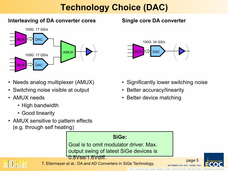
DAC30 Output Waveforms l Measurements performed with
chips mounted in sockets (cf. Slide “Measurement setup“)
l Driven by Virtex-4 (overclocked to 7 Gb/s)
l Measured with Tektronix CSA8000 sampling scope (50 GHz bandwidth)

SEPTEMBER 19-23, 2010 – TORINO, ITALY
page 12 T. Ellermeyer et al.: DA and AD Converters in SiGe Technology.
Signal Impairments through Passive Components • Signal impairments due to passive components
(e.g. traces, cables, connectors, package, etc.)
• Essential but challenging to maintain high frequency performance and effective resolution.
• For example: Reflection • Reflection should be less than 1 LSB:
• Written in dB:
For 8-bit resolution and |r1|=|r2|: è Return loss < -24 dB over the whole
bandwidth on both ends (6-bit: <-18 dB)
r2 r1
DAC
bits ofNumber =≤⋅ brr b21
21
dBdB21 02.6 rbr
−⋅−≤
Reflections in DAC output signal

SEPTEMBER 19-23, 2010 – TORINO, ITALY
page 13 T. Ellermeyer et al.: DA and AD Converters in SiGe Technology.
Topologies for High Speed AD-Converter Cores a) Massive Parallelization (SAR)
• ADC cores typically SAR converters J SAR: Slow but simple architecture / binary
output J Bandwidth is determined by first set of T/H L Clock distribution difficult L Lots of calibration
b) Flash ADC J Extremely fast K Only low resolution:
6 bit => 2^(n-1)=63 comparators in parallel L Complex logic (thermometer code to binary) • Also often used: Half-Flash/Pipeline Flash
c) Interpolation/Folding J Fast flash type converter J Number of comparators reduced to 2^(n-1)/m
by folding m times (typ. m=2) L Complex logic (thermometer code) K Analog stages required
T/H
T/H
ADC
ADCT/H
T/H
ADC
ADCT/H
T/H
T/H
FF
Thermometer -> BinaryDECODE
FFFF FF FF FF FF FF
Massive Parallelization
Flash Converter

SEPTEMBER 19-23, 2010 – TORINO, ITALY
page 14 T. Ellermeyer et al.: DA and AD Converters in SiGe Technology.
Topologies for High Speed AD-Converter Cores
Vin
V3 V0V1V2V4V5
Q1 Q0Q2Q3Q4Q5
CLKQ3Q5 Q4 Q2 Q1 Q0
Vin=V5 V4 V3 V2 V1 V0
d) Serial ripple converter K Little bit slower than flash J Simple architecture (number of amps / flip-flops equal
to resolution) J Direct output of gray coded binary K Highly analog concept K Propagation delay through each stage critical
Integer Binary Gray 0 6‘b000000 6‘b000000 1 6‘b000001 6‘b000001 2 6‘b000010 6‘b000011 … … … 31 6‘b011111 6‘b010000 32 6‘b100000 6‘b110000 33 6‘b100001 6‘b110001 … … … 62 6‘b111110 6‘b100001 63 6‘b111111 6‘b100000

SEPTEMBER 19-23, 2010 – TORINO, ITALY
page 15 T. Ellermeyer et al.: DA and AD Converters in SiGe Technology.
ADC30 Demonstrator Chip
Sampling rate dc – 34 GSa/s
Resolution 6 bit
Full scale input range 282 mV (se or diff)
INL 1.5 LSB
Bandwidth >25 GHz
ENOB (30 GSa/s) 4.7 (fin=7.5 GHz) 3.3 (fin=25 GHz) �
Total power diss. 10 W C o n v e r t e r c o r e power 4 W
Die size 5.07 x 5.07 mm²
Converter size 1.0 x 2.6 mm² �second Nyquist band

SEPTEMBER 19-23, 2010 – TORINO, ITALY
page 16 T. Ellermeyer et al.: DA and AD Converters in SiGe Technology.
• 6 bit serial ripple converter
• Demonstrator with FPGA interface (24 serial lines)
• 34 GSa/s
• Four interleaved cores
• Half rate clock
• Configuration register
ADC30 Demonstrator Chip
5.07 mm
5.07
mm

SEPTEMBER 19-23, 2010 – TORINO, ITALY
page 17 T. Ellermeyer et al.: DA and AD Converters in SiGe Technology.
ADC30 Measurement Results
Upper: l Internal memory mode (16 Samples) l Running at 30 GSa/s (Int. Osc.)
Right: l Data transferred to FPGA
(512kSamples) l Running at 10 GSa/s (FPGA driver
issues)

SEPTEMBER 19-23, 2010 – TORINO, ITALY
page 18 T. Ellermeyer et al.: DA and AD Converters in SiGe Technology.
FPGA/DSP Interface
Current demonstrators based on FPGA constraints: • Use of commercial available FPGA evaluation boards. • Most commonly used is ML525 (Virtex5): 24 RocketIOs • 6-bit resolution; 4x time multiplex => 24 lanes • Raw data transfer to avoid protocol overhead • MGT clock reference is provided by DAC/ADC • Critical:
• RocketIOs show reset dependent delay • Power (50 ohm interfaces)
6.5 Gb/s
26 Gb/s
x6
6x 26 Gb/s
D[5:0]
:20 :26.5 GHzClocks
13 GHzClk
26 GS/s
FPGA DAC
for SR > 26 GS/s FPGA is overclocked
24xRocketIO
REF
MUX DACCore
52xSMA
Cables

SEPTEMBER 19-23, 2010 – TORINO, ITALY
page 19 T. Ellermeyer et al.: DA and AD Converters in SiGe Technology.
FPGA/DSP Interface
Future demonstrators with FPGA interface: • Make use of higher data rates and higher RocketIO count
• Virtex 7: 56x 10 Gb/s and/or 72x 13 Gb/s • Stratix V: 66x 12.5 Gb/s
è Increase Sampling rate and / or number of bits
Next generation: >56 GSa/s / 8 bit
Interface for 3D-packaging with DSP: • Source synchronous • Data rate as high as the DSP/CMOS can handle
(to keep I/O count low) • Free in changing resolution and/or multiplexing
ratio
SEPTEMBER 19-23, 2010 – TORINO, ITALY
page 20 T. Ellermeyer et al.: DA and AD Converters in SiGe Technology.
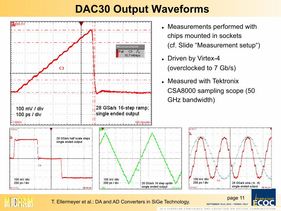
Measurement Setup
Front: Evaluation Board with DAC module
Back: Xilinx ML424 Board with Virtex4-FX140 (24 RocketIOs)
• 15 GHz clock is fed to the DAC module (blue cable)
• Reference clock (:40) for FPGA is generated by DAC
• 48 RF-cables for 24 differential SerDes links
VEGA30G Module

SEPTEMBER 19-23, 2010 – TORINO, ITALY
page 21 T. Ellermeyer et al.: DA and AD Converters in SiGe Technology.
Beyond 100GbE
4-QAM 16-QAM 64-QAM 256-QAM
Bandwidth (GHz)
112 56 37 28
bits/Hz 4 8 12 16
GSa/s 112 56 37 28
ENOB (?) 1 2 3 4
GSa/s 224 112 84 56
ENOB 3.8 4.9 5.7 7.0
DA
C A
DC
Ref: T. Pfau, ECOC‘09
• Next step will be 400 GbE • Data rates up to 448 Gb/s including FEC • Keep WDM grid à higher order modulation formats • DA-converters become mandatory in TX • Very high bandwidth/ENOB à AD-converter may become bottleneck again

SEPTEMBER 19-23, 2010 – TORINO, ITALY T. Ellermeyer et al.: DA and AD Converters in SiGe Technology.
Thank you!