ECEN 622 (ESS) Fall 2011 Practical Issues Designing ...s-sanchez/622 Practical Switched Capacitor...
27
Practical Issues Designing Switched-Capacitor Circuit ELEN 622 Fall 2011 Switched-Capacitor practical issues 1 / 27 Practical Issues Designing Switched-Capacitor Circuit Material partially prepared by Sang Wook Park and Shouli Yan ECEN 622 (ESS) Fall 2011
Transcript of ECEN 622 (ESS) Fall 2011 Practical Issues Designing ...s-sanchez/622 Practical Switched Capacitor...

Practical Issues Designing Switched-Capacitor Circuit
ELEN 622 Fall 2011 Switched-Capacitor practical issues 1 / 27
Practical Issues Designing
Switched-Capacitor Circuit
Material partially prepared by
Sang Wook Park and Shouli Yan
ECEN 622 (ESS) Fall 2011

Practical Issues Designing Switched-Capacitor Circuit
ELEN 622 Fall 2011 Switched-Capacitor practical issues 2 / 27
MOS switch
o Excellent Roff
o Non-idea Effect
Charge injection, Clock feed-through
Finite and nonlinear Ron
Cox Cov Cov
Ron
G
S D
G
S D

Practical Issues Designing Switched-Capacitor Circuit
ELEN 622 Fall 2011 Switched-Capacitor practical issues 3 / 27
Charge Injection
o During TR. is turned on, Qch is formed at channel surface
When TR. is off, Qch1 is absorbed by Vs, but Qch2 is injected to C
o Charge injected through overlap capacitor
o Appeared as an offset voltage error on C
G
VS
Qch1 Qch2
C
( )thGSOXch VVWLCQ −=

Practical Issues Designing Switched-Capacitor Circuit
ELEN 622 Fall 2011 Switched-Capacitor practical issues 4 / 27
Charge Injection Effect
o When clock changes from high to low, Qch2 is injected to C
o Compared to ideal sw., MOS sw. creates voltage error on Vout
Ideal sw.
MOS sw. 1V
0.1pF
CLK
Vout
CLK

Practical Issues Designing Switched-Capacitor Circuit
ELEN 622 Fall 2011 Switched-Capacitor practical issues 5 / 27
Decrease Charge Injection Effect (1)
o Decrease the effect of Qch o Use either bigger C or small TR. (small ratio of Cox/C) o Increased Ron
W/L = 10/0.4
W/L = 1/0.4
1V 0.1pF
CLK
Vout

Practical Issues Designing Switched-Capacitor Circuit
ELEN 622 Fall 2011 Switched-Capacitor practical issues 6 / 27
Decrease Charge Injection Effect (2)
Single sw.
With dummy sw.
o Use dummy switch which provides opposite charge o Adjust size of dummy sw. for exact canceling o Needs opposite clock
1V 0.1pF
CLK
Vout
CLKb
10/0.4 3.1/0.4

Practical Issues Designing Switched-Capacitor Circuit
ELEN 622 Fall 2011 Switched-Capacitor practical issues 7 / 27
Decrease Charge Injection Effect (3)
NMOS sw.
CMOS sw.
o Use N/PMOS complementary switch o Both Qch cancel out due to their opposite polarity o Needs opposite clock, increased parasitic capacitance
1V 0.1pF
CLK
Vout
CLKb
10/0.4
23/0.4

Practical Issues Designing Switched-Capacitor Circuit
ELEN 622 Fall 2011 Switched-Capacitor practical issues 8 / 27
Nonlinear Ron
N/PMOS
NMOS
o Ron varies with signal amplitude o CMOS sw. can adopt large signal o Needs opposite clock, increased parasitic capacitance
Vin
VDD
1.5V
GND
7.5/0.4
18/0.4 PMOS
Vin
Ron

Practical Issues Designing Switched-Capacitor Circuit
ELEN 622 Fall 2011 Switched-Capacitor practical issues 9 / 27
Slow Settling due to high Ron
o Ron varies with signal amplitude o CMOS sw. can adopt large signal o Needs opposite clock, increased parasitic capacitance
Vin
CLK
10pF
Vout
20pF
CLKb
V1

Practical Issues Designing Switched-Capacitor Circuit
ELEN 622 Fall 2011 Switched-Capacitor practical issues 10 / 27
Slow Settling due to high Ron
Ideal sw.
NMOS sw.
o Small NMOS sw. (5/0.4) o With high Ron, output is not settled o In case of large signal input, N/PMOS sw. should be used
Vout
V1
Vout
V1

Practical Issues Designing Switched-Capacitor Circuit
ELEN 622 Fall 2011 Switched-Capacitor practical issues 11 / 27
Slow Settling due to high Ron
Ideal sw.
NMOS sw.
o Large NMOS sw. (20/0.4) o Low Ron makes output settled fast o Close to ideal sw.
Vout
V1
Vout
V1

Practical Issues Designing Switched-Capacitor Circuit
ELEN 622 Fall 2011 Switched-Capacitor practical issues 12 / 27
Switch and Clock Arrangement
M1 M2
M3 M4
M5
M6
C
C3
C1
C2
CK
CKe
CKbe
CKb
CKb
CK
CK CKb
CKe CKbe
o M2, M4 : small sw., Others : large sw. o M2, M4 turn off earlier : minimize charge injection effect o Charge injection
M2, M4 (M3, M6) : Signal independent Others : Signal dependent

Practical Issues Designing Switched-Capacitor Circuit
ELEN 622 Fall 2011 Switched-Capacitor practical issues 13 / 27
Switch and Clock Arrangement
Same sw. (5/0.4) Same CLK
Different sw. (30/0.4, 5/0.4) Early CLK
Ideal sw.

Practical Issues Designing Switched-Capacitor Circuit
ELEN 622 Fall 2011 Switched-Capacitor practical issues 14 / 27
PSS vs. Transient Simulation
o PSS simulation is used to check the frequency response for Switched-capacitor circuit o Should be compared with transient simulation
fin = 100KHz
fin = 10KHz PSS-PAC simulation
fin = 200KHz

Practical Issues Designing Switched-Capacitor Circuit
ELEN 622 Fall 2011 Switched-Capacitor practical issues 15 / 27
Capacitor Layout
o Capacitor is implemented with PIP (poly) or MIM (metal) o Total capacitance is the sum of Cox and Cfr’s o Ratio is more important than absolute value o Multiples of unit capacitor can minimize ratio error o Unit capacitor can be determined by process o Surrounding capacitor bank with dummies is preferred
Cox Cfr Cfr
Cox
Cfr
Cfr Cfr
Cfr
C1
C1
C2
C2 C2
D D D D D
D D D D D
D
D
D
D
D
32
21=
CC

Practical Issues Designing Switched-Capacitor Circuit
ELEN 622 Fall 2011 Switched-Capacitor practical issues 16 / 27
Layout Example
o Example of SC biquad circuit (TSMC 0.35um)

Practical Issues Designing Switched-Capacitor Circuit
ELEN 622 Fall 2011 Switched-Capacitor practical issues 17 / 27
Low Voltage Switched Capacitor Circuits
• Challenges of LV SC circuit design [cas95] – SC circuits are widely used in filters,
data converters, sample and hold, and other analog signal processing building blocks.
– LV SC circuit design is very challenging due to the difficulties involved in turning on MOS switches.
• Solutions – Low and/or multi Vt process – Clock boostering or bootstrap – Switched opamp
GON
VT,P VDD-VT,N
VDD
GON
VDD-VT,N VT,P
VDD
Switch conductance for high VDD(such as 5V)
Switch conductance for low VDD

Practical Issues Designing Switched-Capacitor Circuit
ELEN 622 Fall 2011 Switched-Capacitor practical issues 18 / 27
Low Voltage Switched Capacitor Circuits (Cont’d)
• Low and/or multi Vt process [ada90] – Expensive – Switch leakage while it is off – Vt is not tightly controlled for low
Vt transistors • Clock boostering or bootstrap
– Earlier work ( see right figure ) required that transistors could sustain maximum breakdown voltage of 2Vdd [nak91, cho95, rab98]
– This could not be used in finer technologies due to reduced breakdown voltage
VDD
2VDD
2VDD
0
VDD
0
M1 M2
M3
M4
C1 C2

Practical Issues Designing Switched-Capacitor Circuit
ELEN 622 Fall 2011 Switched-Capacitor practical issues 19 / 27
Low Voltage Switched Capacitor Circuits (Cont’d)
– Constant overdrive bootstrap clock driving solved this problem [abo99]
– Reliability is improved as each transistor just sustains Vdd as maximum voltage
– More power consumption and lower speed due to its complexity – Potential reliability problem during transient
φ1
φ1
φ1
φ1 φ1
A B
VDD
CB
At φ1 CB
VDD
A B
Msw
At φ1
A B
CB Msw

Practical Issues Designing Switched-Capacitor Circuit
ELEN 622 Fall 2011 Switched-Capacitor practical issues 20 / 27
– Detailed schematic and wave form [abo99] • M1, M2, C1, C2 and the inverter could be shared by the switches
with the same phase, other components need to be repeated for every switch.
VDD
M1
M2
C1 C2
M3
C3
M4
M5
M7
M10
M9
M13
M8
φ1
φ1
φ1
Msw
M12 A B
Practical Issues Designing Switched-Capacitor Circuit
ELEN 622 Fall 2011 Switched-Capacitor practical issues 21 / 27
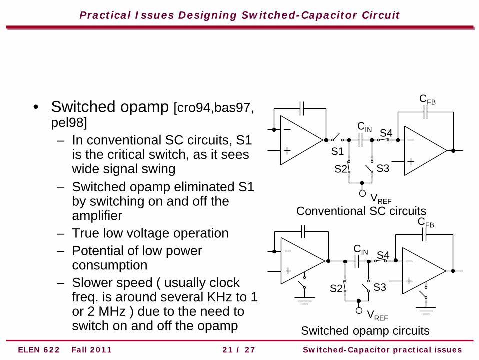
• Switched opamp [cro94,bas97, pel98] – In conventional SC circuits, S1
is the critical switch, as it sees wide signal swing
– Switched opamp eliminated S1 by switching on and off the amplifier
– True low voltage operation – Potential of low power
consumption – Slower speed ( usually clock
freq. is around several KHz to 1 or 2 MHz ) due to the need to switch on and off the opamp
CFB
CIN
S1
S2 S3
S4
VREF Conventional SC circuits
Switched opamp circuits
CFB
CIN
S2 S3
S4
VREF

Practical Issues Designing Switched-Capacitor Circuit
ELEN 622 Fall 2011 Switched-Capacitor practical issues 22 / 27
• Low voltage also poses difficulties for designing the SC Opamps – To maximize output voltage swing, cascoding of output
transistors should be avoided – To achieve required DC gain, two stage architecture may
have to be used instead of single stage OTA – Frequency compensation is an essential issue to make the
amplifier stable and fast settling – Input common mode bias voltage need to close one of the
supply rails to make input transistors operate correctly ( close to Vss -- PMOS input; close to Vdd – NMOS input )
– Input and output need to be biased at different DC levels, level shift may be necessary for switched opamp circuits

Practical Issues Designing Switched-Capacitor Circuit
ELEN 622 Fall 2011 Switched-Capacitor practical issues 23 / 27
• LV SC opamp design example I [abo99] – Two-stage architecture is adopted to achieve high enough
gain – Simple output stage maximizes output voltage swing – First stage is folded-cascode stage with cascode load to
obtain a high gain, as nodes A and B have a small signal voltage swing, and supply voltage and VTN permit this luxury
M1 M2
M3 M4
M6
M8
M10
M5
M7
M9
M11
M13
M15
M12
M14
Cc Cc
VDD=1.5 V
VI+ VI- VO- VO+ A B

Practical Issues Designing Switched-Capacitor Circuit
ELEN 622 Fall 2011 Switched-Capacitor practical issues 24 / 27
– Cascode frequency compensation [ahu83] is used to have a higher bandwidth over conventinal Miller compensation
– The functionality of the circuit is independent of VIN_CM setting, thus VIN_CM could be set to a DC level which makes the amplifier work properly
Cf
Cs
S1
S1
S1
VIN VOUT
1.5b AD
C
output
0 +VR -VR
VIN_CM
The X2 residue amplifier for 1.5b/stage pipeline A/D converter

Practical Issues Designing Switched-Capacitor Circuit
ELEN 622 Fall 2011 Switched-Capacitor practical issues 25 / 27
• LV SC opamp design example II [rab97] – Two-stage architecture with miller compensation – Push-pull operation of the second stage maximize driving
capacity – Two common-mode feedback loops are required to
stablize the bias condition

Practical Issues Designing Switched-Capacitor Circuit
ELEN 622 Fall 2011 Switched-Capacitor practical issues 26 / 27
• LV SC opamp design example III [pel98] – One-stage architecture is used due to relaxed system
requirement for the DC gain – Class AB operation lowers power consumption – Low voltage current mirror makes more room for the input
transistors

Practical Issues Designing Switched-Capacitor Circuit
ELEN 622 Fall 2011 Switched-Capacitor practical issues 27 / 27
References
[abo99] A. M. Abo and P. R. Gray, “A 1.5-V, 10-bit, 14.3-MS/s CMOS pipeline analog-to-digital converter,” IEEE J. Solid-State Circuits, vol. 34, no. 5, pp. 599-606, May 1999 [ada90] T. Adachi, A. Ishikawa, A. Barlow, and K. Takasuka, “A 1.4 V switched capacitor filter,” IEEE CICC 1990, pp. 8.2.1-8.2.4, 1990 [ahu83] B. K. Ahuja, “An improved frequency compensation technique for CMOS operational amplifiers,” IEEE J. Solid-State Circuits, vol. SC-18, no. 6, pp. 629-633, Dec. 1983 [bas97] A. Baschirotto and R. Castello, “A 1-V 1.8-MHz CMOS switched-opamp SC filter with rail-to-rail output swing ,” IEEE J. Solid-State Circuits, vol. 32, no. 12, pp. 1979-1986, Dec. 1997 [cas95] R. Castello, F. Montecchi, F. Rezzi, and A. Baschirotto, “Low-voltage analog filters,” IEEE Trans. Circuits and Systems – I, vol. 42, no. 11, pp. 827-840, Nov. 1995 [cho95] T. B. Cho and P. R. Gray, “A 10 b, 20 Msample/s, 35 mW pipeline A/D converter,” IEEE J. Solid-State Circuits, vol. 30, no. 3, pp. 166-172, March 1995 [cro94] J. Crols and M. Steyaert, “Switched-opamp: an approach to realize full CMOS switched-capacitor circuits at very low power supply voltages,” IEEE J. Solid-State Circuits, vol. 29, no. 8, pp. 936-942, Aug. 1994 [nak91] Y. Nakagome, et al. “An experimental 1.5-V 64-Mb DRAM,” IEEE J. Solid-State Circuits, vol. 26, no. 4, pp. 465-472, April 1991 [pel98] V. Peluso, P. Vancorenland, A. M. Marques, M. S. J. Steyaert, and W. Sansen, “A 900-mV low-power Σ∆ A/D converter with 77-dB dynamic range,” IEEE J. Solid-State Circuits, vol. 33, no. 12, pp. 1887-1897, Dec. 1998 [rab97] S. Rabii and B. A. Wooley, “A 1.8-V digital audio sigma-delta modulator in 0.8 um CMOS,” IEEE J. Solid-State Circuits, vol. 32, no. 6, pp. 783-796, June 1997