ECEN 248 – Introduction to Digital Systems Design (Spring...
21
ECEN 248 – Introduction to Digital Systems Design (Spring 2008) (Sections: 501, 502, 503, 507) Prof. Xi Zhang ECE Dept, TAMU, 333N WERC http://dropzone.tamu.edu/~xizhang/ECEN248
Transcript of ECEN 248 – Introduction to Digital Systems Design (Spring...

ECEN 248 – Introduction to Digital Systems Design (Spring 2008)
(Sections: 501, 502, 503, 507)
Prof. Xi ZhangECE Dept, TAMU, 333N WERC
http://dropzone.tamu.edu/~xizhang/ECEN248

ECEN 248, Spring 2008 X. Zhang
Chapter 3 Implementation Technology
Logic value
Undefined
Logic value
Voltage
V DD
V 1,min
V 0,max
V SS (Gnd)
Figure 3.1. Logic values as voltage levels.

ECEN 248, Spring 2008 X. Zhang
3.1 Transistor Switches
• Most popular type of transistor: Metal Oxide Semiconductor Field-Effect Transistor (MOSFET)
• Two different types of MOSFETs:– 1) N-channel => NMOS transistors– 2) P-channel => PMOS transistors
• Fig. 3.2b is the symbol of NMOS transistor which has 4 electronic terminals:– 1) source; 2) drain; 3) gate; 4) substrate (GND or Body)
• Fig. 3.2c is the simplified symbol of NMOS transistor which the GND connection is omitted where– 1) VS is source terminal; 2) VG is gate terminal; 3) VD

ECEN 248, Spring 2008 X. ZhangFigure 3.2. NMOS transistor as a switch.
Drain Source
x = "low" x = "high"
(a) A simple switch controlled by the input x
V D V S
(b) NMOS transistor
Gate
(c) Simplified symbol for an NMOS transistor
V G
Substrate (Body)

ECEN 248, Spring 2008 X. Zhang
The PMOS Transistors
• PMOS transistors have the opposite behavior of NMOS transistors
• Fig. 3.3a is its logic symbol of PMOS transistor as a logic switch which is “open” if x=“high”, “close if x= “low”.
• Fig. 3.3b is the symbol of PMOS transistor with the substrate terminal always connected to VDD
• Fig. 3.3c is the simplified symbol of PMOS transistor where if VG = “high”, PMOS transistor is turned off; if VG = “low”, PMOS transistor is turned on – as a switch being closed.

ECEN 248, Spring 2008 X. ZhangFigure 3.3. PMOS transistor as a switch.
Gate
x = "high" x = "low"
(a) A switch with the opposite behavior of Figure 3.2 a
V G
V D V S
(b) PMOS transistor
(c) Simplified symbol for a PMOS transistor
V DD
Drain Source
Substrate (Body)
ECEN 248, Spring 2008 X. Zhang
(a) NMOS transistor
V G
V D
V S = 0 V
V S = V DD
V D
V G
Closed switch whenV G = V DD
V D = 0 V
Open switch whenV G = 0 V
V D
Open switch whenV G = V DD
V D
V DD
Closed switch whenV G = 0 V
V D = V DD
V DD
(b) PMOS transistor
Figure 3.4. NMOS and PMOS transistors in logic circuits.
NMOS & PMOS Transistor switch functions/symbols
Summary:

ECEN 248, Spring 2008 X. Zhang
3.2 Logic Gates/Circuits Built on NMOS and PMOS Transistors
• First, we mainly focus on how to implement logic gates/circuits by using NMOS transistors – called NMOS gates/circuits?
• Then, we concentrate on how to implement logic gates/circuits by combining NMOS and PMOS transistors – called Complementary MOS or CMOS gates/circuits, which are presently most popular technology widely used.

ECEN 248, Spring 2008 X. Zhang
(b) Simplified circuit diagram
V x
V f
V DD
x f
(c) Graphical symbols
x f
R
V x
V f
R + -
5 V
(a) Circuit diagram
Figure 3.5. A NOT gate built using NMOS technology.
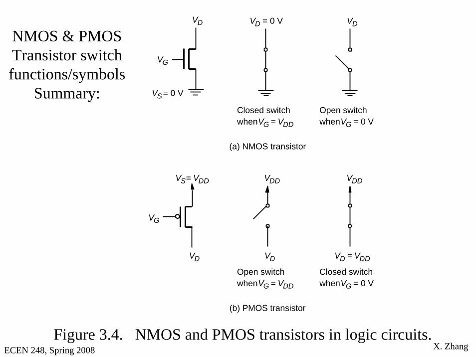
ECEN 248, Spring 2008 X. ZhangFigure 3.6. NMOS realization of a NAND gate.
V f
V DD
(a) Circuit
(c) Graphical symbols
(b) Truth table
f f
0 0 1 1
0 1 0 1
1 1 1 0
x 1 x 2 f
V x 2
V x 1
x 1 x 2
x 1 x 2

ECEN 248, Spring 2008 X. ZhangFigure 3.7. NMOS realization of a NOR gate.
V x 1 V x 2
V f
V DD
(a) Circuit
(c) Graphical symbols
(b) Truth table
f
0 0 1 1
0 1 0 1
1 0 0 0
x 1 x 2 f
f x 1 x 2
x 1 x 2

ECEN 248, Spring 2008 X. ZhangFigure 3.8. NMOS realization of an AND gate.
(a) Circuit
(c) Graphical symbols
(b) Truth table
f f
0 0 1 1
0 1 0 1
0 0 0 1
x 1 x 2 f
V f
V DD
A V x 1
V x 2
x 1 x 2
x 1 x 2
V DD
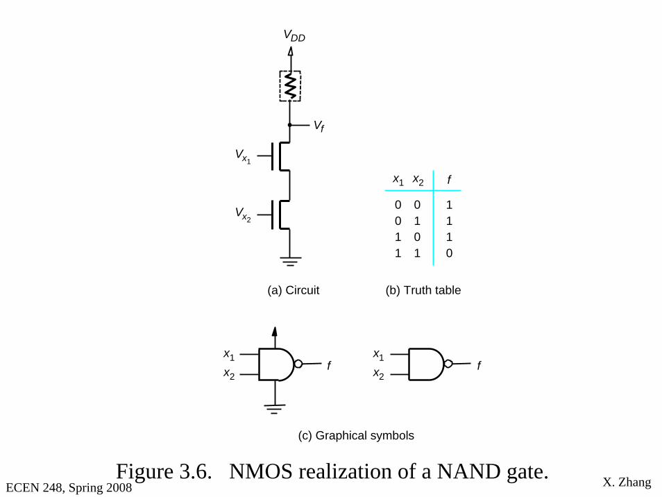
ECEN 248, Spring 2008 X. ZhangFigure 3.9. NMOS realization of an OR gate.
(a) Circuit
(c) Graphical symbols
(b) Truth table
f
0 0 1 1
0 1 0 1
0 1 1 1
x 1 x 2 f
f
V f
V DD
V x 2 V x 1
x 1 x 2
x 1 x 2
V DD

ECEN 248, Spring 2008 X. Zhang
3.3 Logic Gates/Circuits Built on CMOS Transistors
• The logic gates/circuits by combining NMOS and PMOS transistors –called Complementary MOS or CMOS gates/circuits offer some practical implementation advantages over NMOS technology as discussed in Section 3.8.
• In NMOS circuits, the logic functions realized by NMOS transistors combined with a pull-up resistor. We call part of the circuit involving NMOS transistors as the “pull-down network (PDN)”. All NMOS based circuits structures, as shown in Fig 3.5~Fig. 3.8 can be characterized by a block diagram as shown in Fig. 3.10.
• The concept of CMOS circuit is based on the replacing the pull-up device/resistor with a “pull-up network (PUN” that is built using PMOS transistors, such that the functions realized by the PDN and PUNnetworks are complementary as indicated in Fig. 3.11.
• The PDN & PUN have equal number of transistors, which are arranged so that the two networks are “duals” of one another. Whenever the PDN has NMOS transistors connected in series, the PUN has PMOS transistors connected in parallel, and vice versa.

ECEN 248, Spring 2008 X. Zhang
Figure 3.10. Structure of an NMOS circuit.
V f
V DD
Pull-down network V x 1
V x n
(PDN)

ECEN 248, Spring 2008 X. Zhang
Figure 3.11. Structure of a CMOS circuit.
V f
V DD
Pull-down network
Pull-up network
V x 1
V x n
(PUN)
(PDN)
ECEN 248, Spring 2008 X. Zhang
3.3 Basic Logic Gates/Circuits Built on CMOS Transistors and Their Implementation Cost Parameter
• Basic CMOS based NOT gates, NAND gates, NOR gates, and ANG gates with 1 or 2 inputs
• How to implement logic gates/circuits with more than 2 inputs by using CMOS transistors?
• The number of transistors required to build up the gate/circuit with specified functions is the key parameter for implementation expense using the CMOS based logic gates/circuits.
ECEN 248, Spring 2008 X. Zhang
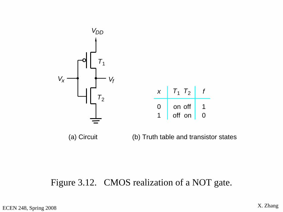
Figure 3.12. CMOS realization of a NOT gate.
(a) Circuit
V f
V DD
V x
(b) Truth table and transistor states
onoff
off on
1 0
0 1
f x T 1 T 2
T 1
T 2

ECEN 248, Spring 2008 X. Zhang
Figure 3.13. CMOS realization of a NAND gate.
(a) Circuit
V f
V DD
(b) Truth table and transistor states
onon
onoff
0 1
0 0 1 1
0 1
off off
onoff
off on
f
off on
1 1 1 0
off off onon
V x 1
V x 2
T 1 T 2
T 3
T 4
x 1 x 2 T 1 T 2 T 3 T 4

ECEN 248, Spring 2008 X. Zhang
(a) Circuit
V f
V DD
(b) Truth table and transistor states
onon
onoff
0 1
0 0 1 1
0 1
off off
onoff
off on
f
off on
1 0 0 0
off off onon
V x 1
V x 2
T 1
T 2
T 3 T 4
x 1 x 2 T 1 T 2 T 3 T 4
Figure 3.14. CMOS realization of a NOR gate.

ECEN 248, Spring 2008 X. Zhang
Figure 3.15. CMOS realization of an AND gate using a NAND gate and a NOT gate.
V f
V DD
V x 1
V x 2
V DD