Ece241 2012 ts_1361464694
13
University of Toronto Faculty of Applied Science and Engineering Department of Electrical and Computer Engineering Midterm Examination ECE 241F - Digital Systems Wednesday October 10, 2012, 6:15 – 7:45 pm Duration: 90 minutes Examiners: J. Anderson, K. Truong, B. Wang ANSWER ALL QUESTIONS ON THESE SHEETS, USING THE BACK SIDE IF NECESSARY 1. No calculators or cell phones are allowed. 2. The number of marks available for each question is indicated in the square brackets []. 3. There are two extra blank pages at the end of the test for rough work. AIDS ALLOWED: Textbook: Fundamentals of Digital Logic with Verilog Design (any edition, but no photocopies), and a single sheet of 8.5” x 11” paper with notes of your choosing. No photocopies of the textbook will be permitted. __________________________________________________________________________________ Last Name: ________________________________________________ First Name: ________________________________________________ Student Number: ________________________________________________ Please Indicate Monday Morning [ ] Which Lab Section Monday Afternoon [ ] You Are In Tuesday Afternoon [ ] Friday Morning [ ] Total Available Marks: Question Q1 Q2 Q3 Q4 Q5 Q6 Q7 Q8 Total Marks Available 9 8 9 10 8 9 9 5 67 Marks Achieved
-
Upload
amadeus2112 -
Category
Education
-
view
20 -
download
1
Transcript of Ece241 2012 ts_1361464694

University of Toronto
Faculty of Applied Science and Engineering
Department of Electrical and Computer Engineering
Midterm Examination ECE 241F - Digital Systems
Wednesday October 10, 2012, 6:15 – 7:45 pm
Duration: 90 minutes Examiners: J. Anderson, K. Truong, B. Wang
ANSWER ALL QUESTIONS ON THESE SHEETS, USING THE BACK SIDE IF NECESSARY 1. No calculators or cell phones are allowed. 2. The number of marks available for each question is indicated in the square brackets []. 3. There are two extra blank pages at the end of the test for rough work. AIDS ALLOWED: Textbook: Fundamentals of Digital Logic with Verilog Design (any edition, but no photocopies), and a single sheet of 8.5” x 11” paper with notes of your choosing. No photocopies of the textbook will be permitted. __________________________________________________________________________________ Last Name: ________________________________________________ First Name: ________________________________________________ Student Number: ________________________________________________ Please Indicate Monday Morning [ ] Which Lab Section Monday Afternoon [ ] You Are In Tuesday Afternoon [ ] Friday Morning [ ] Total Available Marks:
Question Q1 Q2 Q3 Q4 Q5 Q6 Q7 Q8 Total Marks Available
9 8 9 10 8 9 9 5 67
Marks Achieved

[9] Q1. For this question, use algebraic manipulation to find the minimized SOP or POS expressions. Specify the rules of Boolean algebra used for simplification in each step. Higher marks will be given to solutions using fewer steps. i) Use Boolean algebra to minimize the following expression. Your final answer should be the minimal SOP form for this function. [2]
dcabdcbadcbaddaf ++++= Solution: = d + bc’d+a’bc’d’+abc’d’ Combining = d + bc’d + bc’d’ Combining = d + bc’ Combining ii) Use Boolean algebra to minimize the following expression. Your final answer should be the minimal SOP form for this function. [3]
))()(())(( zyxyxwxzxyxf +++++++= Solution: =(x+y)(x+z)+(x+w)(x+y) Covering =(x+y)((x+z)+(x+w)) Distributivity = (x + y)(x+w+z) = x + y(w+z) Distributivity = x + yw+yz Distributivity iii) Use Boolean algebra to minimize the following expression. Your final answer should be the minimal POS form for this function. [4]
cadcaf ++= Solution: = ac’ +(c+d)(a’+d) Distributivity = (ac’ + c + d)( ac’ + a’ + d) Distributivity = (ac’ + ac + c + d ) ( ac’ + a’c’ + a’ + d) Covering =(a+c+d)(a’+c’+d) Combining
[8] Q2. Using the K-map below, determine which gate(s) can be removed from the following circuit to reduce the cost (total number of gates + total number of inputs) as much as possible. Show your work. Note: you may not create any new gates, only remove the existing one(s), and you may not remove individual inputs to an AND gate unless the entire AND gate is to be removed.
gate 6
gate 4gate 1
gate 9gate 2
gate 3
gate 5
gate 7
gate 8
w
x
y
z
f
0 0 1 0
0 0
1 1
0 1
0 1y zw x
1 0
1 1
1 1
1 1
1 1
111
gate 8
gate 5
gate 4 gate 7gate 6
f = w’yz’ + xy’z’ + wx + xz’ + wz
gate ○4 ○5 ○6 ○7 ○8
minimal cover SOP form is: f = w’yz’ + xz’ + wz
gate ○4 ○7 ○8
Gates to remove are: 2, 5 and 6.
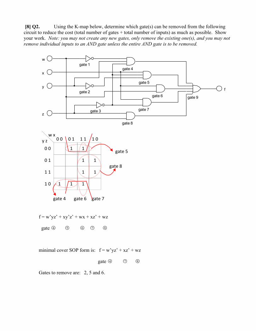
[9] Q3. i) Diane built the logic circuit shown below, the logic probe is always OFF (0) whether the switch is in position A or B. Is the problem with the inverter or the NOR, or is there no problem? Explain your answer. [4]
123456
8910111213Vcc
Gnd
74LS02
Quad 2-‐input NOR
123456
8910111213Vcc
Gnd
74LS04/05
Hex INVERTER
5 VSwitch Logic Probe
A
B
Switch ( 0 )
( 0 )( 1 )Probe
Switch ( 1 )
( 0 )( 0 )Probe
There is no problem with this circuit.
ii) Bobby constructed the same circuit as Diane on his protoboard, the logic probe’s light comes ON (1) when the switch is in position B. Further testing with the probe shows that pins 2 and 3 of the NOR IC are both LOW (0). Is anything wrong? If so, where is the fault? [2]
Switch ( 0 )
( 1 )( 0 )Probe
There is a problem with the inverter, a good inverter should output a “1” for an input of “0” in this case, consequently produces a “0” at the Probe.

iii) The logic circuit in (a) shown below is implemented by making connections to the 7400 IC chip as shown in (b). The circuit is not working properly. The problem could either be in the IC connections or in the IC itself. The data table in (c) is completed by using a logic probe at each pin. Identify the problem and explain why. [3]
123456
8910111213Vcc
Gnd
74LS00/03
Quad 2-‐input NAND
AB
XC
(a)
(b)(c)
A
BC
X
+ 5 V1234567891011121314
OnOnOffOffOffOffOffOnDimDimOnOnOffOn
Probe on pin: Indicator light
Test conditions:A=1, B=1, C=1, X should equal 0
1
2
3
4
ABC x
1 23
Gate 1 and gate 3 function properly, but gate 2 has defect.

[10] Q4. A 7-segment display has 7 individual segments (a to g) which can be turned “on” or “off” individually to display alphabetic characters. You are asked to display the word LOGIC as follows:
i) Assuming that each letter from the word LOGIC is selected with a 3-bit (xyz) code, complete the truth table below for all segments (a to g). Assume that a segment turns “on” when a logic 1 is asserted. [3] x y z a b c d e f g L 0 0 0 0 0 0 1 1 1 0 O 0 0 1 1 1 1 1 1 1 0 G 0 1 0 1 0 1 1 1 1 1 I 0 1 1 0 0 0 0 1 1 0 C 1 0 0 1 0 0 1 1 1 0 1 0 1 x x x x x x x 1 1 0 x x x x x x x 1 1 1 x x x x x x x ii) Fill in the K-maps below for output segments a, b and c only. [1]
0 0 1 0
0
1 1
1
0 1zx y
a
0 0 1 0
0
1 1
1
0 1zx y
b
0 0 1 0
0
1 1
1
0 1zx y
c
1
1
1
1 1
1 x
x x
x
x x
x
x x

iii) Find the SOP expressions for a, b and c in order to achieve minimum total cost (consider sharing gates). [4] a = y’z + yz’ + x b = y’z c = y’z + yz’ iv) Draw a multi-output logic circuit implementation that produces the outputs a, b and c using only AND, OR, and NOT gates. Your circuit should implement the functions determined in step iii) [2]
a
b
c
xy
z

18] Q5. Consider the following logic circuit:
i) Write the logic function forf in -of-sums (POS) form: [2]
ar-x2
x,
x4
Tx3
3
=[E*?L) Cr.r r xt(Fr +15 - E)
ii) Draw a logic function for/using a minimum number of NAND gates. You may only use NANDgates, and your NAND gates may have either 2 or 3 inputs. In your circuit, you may assume that thecircuit input signals (x1, x2, X3 Bnd v) are freely available in both true and complemented form. [6]
[.KL
\lxrf s
f= X, Xt t KrKzK: r T,^r[',
Srx1
I!-ituir;
n\r|-'Jn\*---
\ \ \\ci-
\clc
o\
\ \ (
\c
le D c
( \ EpTml \
en

I9l Q6. The left-side of the figure below shows the circuit symbol for a gated D latch (i.e. atransparent latch). A gated D latch can be imalemented with the gates shown on the right-side of thefigure.
i)'fmplernont a gated D latqh using the logic gates provided, You only need to add connectionsbetween the gates and label the input and output signals. Your circuit does not need to generate thecomplemented form of Q. [a]
ii) Complete the timing diagrarn (see next page) for the circuit below. The flip-flbps are positive edge-triggered. You may assume delays are zero. You may further assume that Qo, Qr and Qz are allinitially logic-0. [4]

*
Os
a,
el
iii) Given thal
i ;
i r
the above circuit do? [1
Cor^-*s \^oN\r1 ,9r3
sq\Ls Q-
) \,3, +u u- I'o&'{ '3* ['JG*S,
*

I9l Q7. Consider a circuit with three single-bit inputs Sz, Sr, Ss, and three single-bit outputs Zz,ZrZo.The three inputs represent a3-bitnumber in binary (Sz is the most-significant bit), and likewise, thethree outputs represent a 3-bit number in binary (Z2is the most-significant bit). Design a circuitwhere, if the binary value of the input is 0,1,2 or 3, then the binary value of the output should be onegreater than the input. If the binary value of the input is 4,5,6, or 7, then the binary value of theoutput should be one less thanthe input.
i) Draw the truth table for your 3-input, 3-output circuit. [3]
)7 2 t 2o 2- ?', Zo
ii) Use K-maps to derive minimized logic expressions for the three
2,
\
o\
O\
o\
ooutputs. [3]
O
l\
o\
c>ot
<_-/(>
()
\
O(
tt
oIoIoIb
I
ooI\()
oII
oC2o
(
5r€ooo \ l o
?z= 5,4\ 529o t SzSr
2 f 5,-O s,6 so
L cau q\so u'"' *o \ n! -{Pr
" ')
2rs
So(
5"
ob '
o o t o (
o\t o L
t') ^. -E
zho

iii) Write procedural Verilog code for the 3-input, 3-output circuit. Your Verilog code must use analways block. [3]
hroJ,^,Q.s crJr C Sr Z)'t
r"1,,^t- lz:* S;
ow\q.r* , ") l2tot 2 |
. \
fu"fe(s )btlK / <- )t - gllJ 'n I
t( (> 1--
+= S+(2
e\sq c
,bo\Dt' [[i1' b|t)
c^dt U---
ev\{ w'o Ql L
'' 6LnO(h{rro2---t"-
ocs)
dUV-
beAr"rv'0 )fo1= ruSeil . L)cd='saiisufa
5DA/
d--€DilS{L \:cu'ca\<r^=L
D sct$s(z)^,

[5] Q8.
i) Using a minimum number of 2-to-1 multiplexors, implement a 2-input OR gate. [2] Solution: S=X I[0] = Y I[1] = 1
ii) Using a minimum number of 2-to-1 multiplexors, implement a 3-input AND gate. [3] Solution: S1=Y I1[0] = 0 I1[1] = X S2= F1 I2[0] = 0 I2[1] = Z