17.384 Microprocessors B Lab 4 Spring 2012 Motor Control ...

EC1019A PROCESSOR LAB
LABORATORY MANUAL
SEMESTER V
DEAPRTMENT OF ELECTRONICS AND COMMUNICATION ENGINEERING
SRM UNIVERISTY (Under SECTION 3 of the UGC Act, 1956)
S.R.M. NAGAR, KATTANKULATHUR – 603203.

2
Department of Electronics and Communication Engineering
EC1019A
Processor Lab
Laboratory Manual
June 2015
Mr. R.Prithiviraj. and course committee

3
L T P C
EC1019A PROCESSOR LAB 0 0 3 2
Prerequisite : nil
PURPOSE : This laboratory will provide the students a perfect introduction to the world of Microprocessors and to provide hands‐on experience essential to the real understanding of microprocessors architecture and it’s interfacing to the peripheral devices. The experiments are designed to provide the students with the design principles of microprocessor systems and real time programming. The course accomplishes this by using microprocessor kits, simulators and software development systems. INSTRUCTIONAL OBJECTIVES 1.To demonstrate programming proficiency using the various addressing modes and data transfer instructions of the target microprocessor. 2.To apply knowledge of the microprocessor’s internal registers and operations by use of a PC based microprocessor simulator. 3.To interface the processor to external devices
LIST OF EXPERIMENTS
S.No.
Lab Experiments
1 Introduction to microprocessor and microcontroller kit.
2 Introduction to registers , Instruction sets, arithmetic operators of 8086
3 Introduction to General purpose registers, addressing modes, logical operators of
8086
4 Interfacing of 8255 PPI with 8086
5 Interfacing of 8279 keyboard and display with 8086
6 Introduction to registers , Instruction sets, arithmetic operators of 8051
7 Introduction to General purpose registers, addressing modes, logical operators of
8051
8 Interfacing of 8254 timer with 8051 Microcontroller
9 Interfacing of Stepper motor control with 8051 Microcontroller
10 Implementation of Seven segment display from ‘0000’ to ‘9999’ using Nuvoton
board
11 Implementation of Seven segment display for ADC input using Nuvoton board
12 Implementation of UART using Nuvoton board
13 Implementation of temperature sensor using Nuvoton board
14 Linear convolution using TMS320C6713 kit
15 Circular convolution using TMS320C6713 kit

4
EC1019A – Processor Lab
Course designed by Department of Electronics & Communication Engineering
1 Program outcome
A b c d e f g h i j k X X X X X
2 Category General (G)
Basic Sciences
(B)
Engineering Sciences and
Technical Arts(E)
Professional Subjects(P)
X 3 Broad area
(for ‘P’category)
Communication Signal Processing Electronics VLSI Embedded
X
4
Staff responsible
for preparing the syllabus
Mr. A.V.M Manikandan Mr. Selvakumar
5 Date of preparation May 2014

5
S.R.M University Faculty of Engineering and Technology
Department of Electronics and Communication Engineering Sub Code: EC1019A Semester : V Sub Title: Processor Lab Course Time: Jul–Dec’15 Pre‐requisite : NIL Co‐requisite : EC1016A Microprocessors & Microcontrollers
Program Outcome
c. Graduate will demonstrate the ability to design and conduct experiments, analyze and interpret data
Experiment 1 to Experiment no. 15 (Please refer Expt. list)
d. Graduate will demonstrate the ability to design a system, component or process as per needs and specification
Experiment 4: To interface 8255 Programmable Peripheral Interface with 8086 microprocessor and to test mode 0 operation
Experiment 5: To interface Keyboard /Display to 8086 micro controller and to read key and display data in leds.
Experiment 8: To interface 8254 programmable timer with 8051 controller and to test the mode 0 operation.
Experiment 9: To interface a stepper motor with a 8051 kit and to make it run a) clockwise b) anti clockwise
e. an ability to identify, formulate, and solve engineering problems
Experiment 1 to Experiment no. 15 (Please refer Expt. list)
f. Graduate will demonstrate the skills to use modern engineering tools, software’s and equipment to analyze problems
Experiment 2: Using 8086 emulator add, subtract, multiply and divide two 16 bit numbers stored in the memory and save the results of the operation in the memory.
Experiment 3: To find the largest and the smallest of the given array of numbers stored in memory using 8086.
Experiment 3: To sort the given array of numbers stored in memory location into ascending and descending order using 8086.
Experiment 10: Perform seven segment display from “0000” to “9999’ in Keil IDE
Experiment 11: Perform seven segment display fetching data from the potentiometer using Keil IDE
(j) a knowledge of contemporary issues
Experiment 1 to Experiment no. 15 (Please refer Experiment list)

6
S.R.M University Faculty of Engineering and Technology
Department of Electronics and Communication Engineering Sub Code : EC1019A Semester : V Sub Title : Processor Lab Course Time : Jul–Dec’15 Pre_requisite : NIL Co_requisite : EC01016A Microprocessors & Microcontrollers
Program Educational Objectives Vs Program Outcome
Program Educational Objective
PEO1: Graduates will perform as a successful Professional engineer in related fields of Electronics and Communication Engineering.
PEO2: Graduates will pursue higher education and/or engage themselves in continuous professional development to meet global standards.
PEO3: Graduates will work as a team in diverse fields and gradually move into leadership positions.
PEO4: Graduates will understand current professional issues, apply latest technologies and come out with innovative solutions for the betterment of the nation and society.
Student Outcomes
c √ √
d √ √ √
e √ √
f √ √ √ √
j √ √ √
7
S.R.M University Faculty of Engineering and Technology
Department of Electronics and Communication Engineering
Sub Code : EC1019A Semester : V Sub Title : Processor Lab Course Time : Jul–Dec’15 Pre_requisite : NIL Co_requisite : EC1016A Microprocessors & Microcontrollers
Instructional Objective and Program Outcome
S.No Instructional Objective
Program Outcome Experiment Details
1 To demonstrate program proficiency using the various addressing modes and data transfer instructions of the target microprocessor.
d. Graduate will demonstrate the ability to design a system, component or process as per needs and specification
1.Introduction to microprocessor and microcontroller kit. 2.Introduction to registers , Instruction sets, arithmetic operators of 8086 3. Introduction to General purpose registers, addressing modes, logical operators of 8086
e. an ability to identify, formulate, and solve engineering problems f. Graduate will demonstrate the skills to use modern engineering tools, software’s and equipment to analyze problems j. a knowledge of contemporary issues c. Graduate will demonstrate the ability to design and conduct experiments, analyze and interpret data
2 To apply knowledge of the microprocessor’s internal registers and operations by use of a PC based microprocessor simulator.
d. Graduate will demonstrate the ability to design a system, component or process as per needs and specification
6.Introduction to registers , Instruction sets, arithmetic operators of 8051 7.Introduction to General purpose registers, addressing modes, logical operators of 8051
e. an ability to identify, formulate, and solve engineering problems f. Graduate will demonstrate the skills to use modern engineering tools, software’s and equipment to analyze problems c. Graduate will

8
demonstrate the ability to design and conduct experiments, analyze and interpret data
3 To interface the processor to external devices.
d. Graduate will demonstrate the ability to design a system, component or process as per needs and specification
4.8255 PPI using 8086 5.8279 keyboard and display using 8086 8.8254 timer using 8051 Microcontroller 9.Stepper motor control using 8051 Microcontroller 10.Seven segment display using NUVOTON board. 11.ADC using NUVOTON board. 12. UART using NUVOTON board. 13. Temperature sensor using NUVOTON board 14. Linear convolution using TMS320C6713 kit. 15. Circular convolution using TMS320C6713 kit
e. an ability to identify, formulate, and solve engineering problems f. Graduate will demonstrate the skills to use modern engineering tools, software’s and equipment to analyze problemsj. a knowledge of contemporary issues

9
S.R.M University Faculty of Engineering and Technology
Department of Electronics and Communication Engineering Sub Code : EC0321 Semester : V Sub Title: Processor Lab Course Time : Jul–Dec’14 Pre_requisite : NIL Co_requisite : EC0309 Microprocessors & Microcontrollers
EXPERIMENTS DETAILS
S.No. Experiments Detail Equipments Required
Components Required
I.Programming in 8086 1 Introduction to microprocessor and
microcontroller kit. 8086 Trainer Kit Power Cables
2 Introduction to registers , Instruction sets, arithmetic operators of 8086
8086 Trainer Kit Power Cables
3 Introduction to General purpose registers, addressing modes, logical operators of 8086
8086 Trainer Kit Power Cables
II. 8086 Interfacing
4 Interfacing of 8255 PPI using 8086 8086 Trainer Kit, 8255
Power Cables
5 Interfacing of 8279 keyboard and display using 8086
8279 module, 8051 kit
Power Cables Add on card connector bus.
III.Programming in 8051
6 Introduction to registers , Instruction sets, arithmetic operators of 8051
8051 Trainer kit Power Cables
7 Introduction to General purpose registers, addressing modes, logical operators of 8051
8051 Trainer kit Power Cables
IV.8051 Interfacing
8 Interfacing of 8254 timer using 8051 Microcontroller
8253 module, 8051 kit
Power Cables
9 Interfacing of Stepper motor control using 8051 Microcontroller
Stepper motor , 8051 kit
Power Cables
V. Programming in Nuvoton Board 10 Implementation of Seven segment display
from ‘0000’ to ‘9999’using Nuvoton board Nuvoton kit Power Cables
11 Implementation of Seven segment display for ADC input using Nuvoton board
Nuvoton kit, Potentiometer
Power Cables
12 Implementation of UART using Nuvoton board
Nuvoton kit Power Cables
13 Implementation of temperature sensor using Nuvoton board
Nuvoton kit Power Cables
VI. Programming in TMS320C6713 Digital signal processor
14 Linear convolution using TMS320C6713 kit TMS320C6713 kit
Power Cables
15 Circular convolution using TMS320C6713 kit TMS320C6713 kit
Power Cables
10
Academic Course Description
SRM UniversityFaculty of Engineering and Technology
Department of Electronics and Communication Engineering
EC1019A Processor lab Fifth Semester, 2015‐16 (OddSemester)
Course (catalog) description
This Microprocessor is a required course for under‐graduate students in the ECE program. The purpose of this course is to teach students the fundamentals of microprocessor and microcontroller systems. The student will be able to incorporate these concepts into their electronic designs for other courses where control can be achieved via a microprocessor/controller implementation.
Topics include Semiconductor memory devices and systems, microcomputer architecture,assembly language programming, I/O programming, I/O interface design, I/O peripheral devices, datacommunications, and data acquisition systems. Several laboratory exercises will be based on both microprocessor (Intel 8086), microcontroller (Intel 8051) and ARM (nuvoTon‐ Nu‐LB‐LUC140)).
Compulsory/Elective course: Compulsory Credit hours: 2 credits Laboratory Digital signal processing Laboratory (TP9L3) , Computing Laboratory (TP10L1), RF Laboratory (TP13L4) Course coordinator(s) R.PRITHIVIRAJ, Assistant Professor (Ordinary Grade), Department of ECE INSTRUCTOR(S)
Name of the instructor
Class handling
Office location
Office phone
Email(@ktr.srmuniv.ac.in) Consultations
Mrs. R. Manohari X1 TP9S4 2055 manohari.r Day 5‐12.45PM to 1.20PM
Mr. R. Prithiviraj X2 TP10S4 ‐‐ prithiviraj.r Day 5‐12.45PM to 1.20PM
Dr.Diwakar.R.marur X3 TP1003A ‐‐ Diwakar.r Day 5‐12.45PM to 1.20PM
Mr. S. Yuvaraj X4 TP10S4 ‐‐ yuvaraj.s Day 5‐12.45PM to 1.20PM .
Mr. A. Joshua Jafferson X5 TP1206A 2067 joshua.j Day 5‐12.45PM to 1.20PM .
Ms.D. Vijayalakshmi Y1 TP1203A 2064 vijayalakshmi.d Day 5‐12.45PM to 1.20PM
Mr. K. Ramesh Y2 TP1106A 2063 ramesh.kr Day 5‐12.45PM to 1.20PM .
Mrs. J. K. KasthuriBha Y3 TP10S8 2070 kasthuribha.jk Day 5‐12.45PM to 1.20PM .

11
Name of the instructor
Class handling
Office location
Office phone
Email(@ktr.srmuniv.ac.in) Consultations
Mr. M. Maria Dominic Savio Y4 TP10S4 ‐‐ mariadominicsavio
.m Day 5‐1.45PM to 3.20PM .
Mrs. K. Ferents Koni Jiavana Y5 TP10S8 2061 ferentskoni.k Day 5‐12.45PM to
1.20PM .
Mr. A.Sriram Y6 TP103A 2065 sriram.a Day 5‐3.45PM to 4.40PM .
RELATIONSHIP TO OTHER COURSES Pre‐requisites : NIL Following courses : Nil Text book(s) and/or required materials:
Lab manual; additional materials posted on SRM web.
References
1. Processor Lab MANUAL, Department of ECE, SRM University 2. Ray.A.K and Bhurchandi.K.M, “Advanced Microprocessors and Peripherals”, Tata
McGraw‐Hill, 2006. 3. Muhammad Ali Mazidi and Janice Gillispie Mazidi, Rolin D. McKinlay, “The 8051
– Microcontroller and Embedded Systems: Using Assembly and C”, 2nd Edition, Pearson Education, 2011.
4. Nuvoton (NUC100/140 series Board Schematics manual, nuvoTon (NUC100/140) series Educational sample codes), www.nuvoton.com
Computer usage
Students are expected to use the computer to write and assemble assembly language programs and also run them by downloading them to the target microprocessor. Students will also use a microprocessor software simulator that runs on the personal computer. Students will also prepare lab reports and conduct out‐of‐class assignments using the computer.
Class / Lab schedule : one 100 minutes lab session per week, for 10‐14 weeks
Group Schedule X1 DAY 1 – 7, 8 & DAY 2 ‐ 3,4 X2 DAY 1 – 7, 8 & DAY 4 – 1,2 X3 DAY 3 – 7, 8 & DAY 5 ‐ 3,4 X4 DAY 2 – 3, 4 & DAY 3 ‐ 7,8 X5 DAY 2 – 3, 4 & DAY 5 ‐ 7,8 Y1 DAY 2 – 7, 8 & DAY 5 ‐ 3,4 Y2 DAY 2 – 7, 8 & DAY 3 ‐ 3,4 Y3 DAY 3 – 3, 4 & DAY 4 ‐ 7,8 Y4 DAY 3 – 3, 4 & DAY 5 ‐ 7,8 Y5 DAY 4 – 7, 8 & DAY 5 ‐ 3,4 Y6 DAY 1 – 7, 8 & DAY 4 ‐ 1,2
12
Professional component General ‐ 0% Basic Sciences ‐ 0% Engineering sciences & Technical arts ‐ 0% Professional subject ‐ 100%
Broad area: Communication | Signal Processing | Electronics | VLSI | Embedded
Mapping of Instructional Objectives with Program Outcome This course provides the foundation education in Microprocessor and microcontroller. Through lecture, laboratory, and out‐of‐class assignments, students are provided learning experiences that enable them to:
Correlates to Student Outcome
H M L
1. To demonstrate program proficiency using the various addressing modes and data transfer instructions of the target microprocessor.
c, d e j
2. To apply knowledge of the microprocessor’s internal registers and operations by use of a PC based microprocessor simulator.
c, d j f
3. To interface the processor to external devices. c, d e f,j
H: High correlation, M: Medium correlation, L: Low correlation
Course Learning Outcomes 1. Students should be able to solve basic binary math operations using the
microprocessor / microcontroller
2. Students should be able to demonstrate programming proficiency using the various addressing modes and data transfer instructions of the target microprocessor / microcontroller.
3. Students should be able to program using the capabilities of the stack, the program counter, and the status register and show how these are used to execute a machine code program.
4. Students should be able to apply knowledge of the microprocessor’s internal registers and operations by use of a PC based microprocessor simulator.
COURSE TOPICS S.No. Lab Experiments Sessions 1 Introduction to microprocessor and microcontroller kit. 1
2 Introduction to registers , Instruction sets, arithmetic operators of 8086 2
3 Introduction to General purpose registers, addressing modes, logical operators of 8086 3
4 Interfacing of 8255 PPI with 8086 4 5 Interfacing of 8279 keyboard and display with 8086 5
6 Introduction to registers , Instruction sets, arithmetic operators of 8051 6
7 Introduction to General purpose registers, addressing modes, logical operators of 8051 7
8 Interfacing of 8254 timer with 8051 Microcontroller 8 9 Interfacing of Stepper motor control with 8051 Microcontroller 9
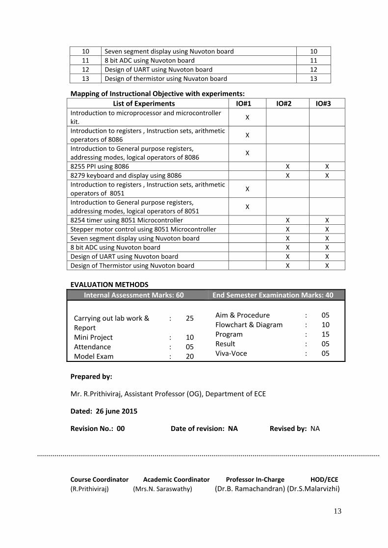
13
10 Seven segment display using Nuvoton board 10 11 8 bit ADC using Nuvoton board 11 12 Design of UART using Nuvoton board 12 13 Design of thermistor using Nuvaton board 13
Mapping of Instructional Objective with experiments: List of Experiments IO#1 IO#2 IO#3
Introduction to microprocessor and microcontroller kit. X
Introduction to registers , Instruction sets, arithmetic operators of 8086 X
Introduction to General purpose registers, addressing modes, logical operators of 8086 X
8255 PPI using 8086 X X 8279 keyboard and display using 8086 X X Introduction to registers , Instruction sets, arithmetic operators of 8051 X
Introduction to General purpose registers, addressing modes, logical operators of 8051 X
8254 timer using 8051 Microcontroller X X Stepper motor control using 8051 Microcontroller X X Seven segment display using Nuvoton board X X 8 bit ADC using Nuvoton board X X Design of UART using Nuvoton board X X Design of Thermistor using Nuvoton board X X EVALUATION METHODS
Internal Assessment Marks: 60 End Semester Examination Marks: 40
Carrying out lab work & Report
: 25
Mini Project : 10 Attendance : 05 Model Exam : 20
Aim & Procedure : 05 Flowchart & Diagram : 10 Program : 15 Result : 05 Viva‐Voce : 05
Prepared by:
Mr. R.Prithiviraj, Assistant Professor (OG), Department of ECE
Dated: 26 june 2015
Revision No.: 00 Date of revision: NA Revised by: NA
Course Coordinator Academic Coordinator Professor In‐Charge HOD/ECE (R.Prithiviraj) (Mrs.N. Saraswathy) (Dr.B. Ramachandran) (Dr.S.Malarvizhi)

14
LABORATORY POLICIES AND REPORT FORMAT
Reports are due at the beginning of the lab period. The reports are intended to be a complete documentation of the work done in preparation for and during the lab. The report should be complete so that someone else familiar with electronic design could use it to verify your work. The prelab and postlab report format is as follows:
1. A neat thorough prelab must be presented to your faculty Incharge at the beginning of your scheduled lab period. Lab reports should be submitted on A4 paper. Your report is a professional presentation of your work in the lab. Neatness, organization, and completeness will be rewarded. Points will be deducted for any part that is not clear.
2. In this laboratory students will work in teams of three. However, the lab
reports will be written individually. Please use the following format for your lab reports.
a. Cover Page: Include your name, Subject Code, Section No., Experiment No. and Date.
b. Objectives: Enumerate 3 or 4 of the topics that you think the lab will teach you. DO NOT REPEAT the wording in the lab manual procedures. There should be one or two sentences per objective. Remember, you should write about what you will learn, not what you will do.
c. Design: This part contains all the steps required to arrive at your final circuit. This should include diagrams, tables, equations, explanations, etc. Be sure to reproduce any tables you completed for the lab. This section should also include a clear written description of your design process. Simply including a circuit schematic is not sufficient.
d. Questions: Specific questions (Prelab and Postlab) asked in the lab should be answered here. Retype the questions presented in the lab and then formally answer them.
3. Your work must be original and prepared independently. However, if you
need any guidance or have any questions or problems, please do not hesitate to approach your faculty incharge during office hours. Copying any prelab/postlab will result in a grade of 0. The incident will be formally reported to the University and the students should follow the dress code in the Lab session.
4. Each laboratory exercise (circuit) must be completed and demonstrated to
your faculty Incharge in order to receive working circuit credit. This is the procedure to follow:
a. Circuit works: If the circuit works during the lab period (2 hours), call your faculty incharge, and he/she will sign and date it.. This is

15
the end of this lab, and you will get a complete grade for this portion of the lab.
b. Circuit does not work: If the circuit does not work, you must make use of the open times for the lab room to complete your circuit. When your circuit is ready, contact your faculty incharge to set up a time when the two of you can meet to check your circuit.
5. Attendance at your regularly scheduled lab period is required. An
unexpected absence will result in loss of credit for your lab. If for valid reason a student misses a lab, or makes a reasonable request in advance of the class meeting, it is permissible for the student to do the lab in a different section later in the week if approved by the faculty incharge of both the sections. Habitually late students (i.e., students late more than 15 minutes more than once) will receive 10 point reductions in their grades for each occurrence following the first. Student attendance less than 75% is detention.
6. Final grade in this course will be based on laboratory assignments. All labs
have an equal weight in the final grade. Grading will be based on pre‐lab work, laboratory reports, post‐lab and in‐lab performance (i.e., completing lab, answering laboratory related questions, etc.,).The faculty Incharge will ask pertinent questions to individual members of a team at random. Labs will be graded as per the following grading policy:
Attendance ‐ 05%
Lab Performance ‐ 10%
Prelab ‐ 05%
Post Lab ‐ 05%
Report ‐ 05%
Student Contribution ‐ 10%
Model Exam ‐ 20%
Final exam ‐ 40%
7. Reports Due Dates: Reports are due one week after completion of the corresponding lab.
8. Systems of Tests: Regular laboratory class work over the full semester will carry a weightage of 60%. The remaining 40% weightage will be given by conducting an end semester practical examination for every individual student if possible or by conducting a 1 to 1 ½ hours duration common written test for all students, based on all the experiment carried out in the semester.
16
ADDENDUM
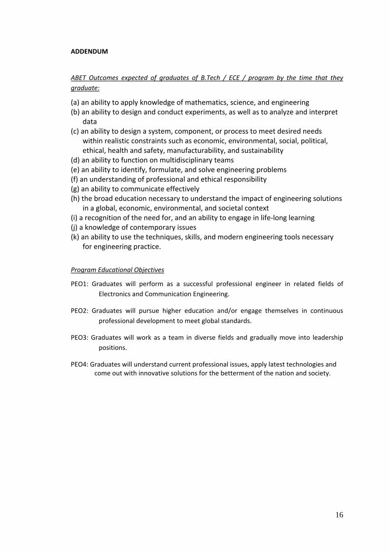
ABET Outcomes expected of graduates of B.Tech / ECE / program by the time that they graduate:
(a) an ability to apply knowledge of mathematics, science, and engineering (b) an ability to design and conduct experiments, as well as to analyze and interpret
data (c) an ability to design a system, component, or process to meet desired needs
within realistic constraints such as economic, environmental, social, political, ethical, health and safety, manufacturability, and sustainability
(d) an ability to function on multidisciplinary teams (e) an ability to identify, formulate, and solve engineering problems (f) an understanding of professional and ethical responsibility (g) an ability to communicate effectively (h) the broad education necessary to understand the impact of engineering solutions
in a global, economic, environmental, and societal context (i) a recognition of the need for, and an ability to engage in life‐long learning (j) a knowledge of contemporary issues (k) an ability to use the techniques, skills, and modern engineering tools necessary
for engineering practice.
Program Educational Objectives
PEO1: Graduates will perform as a successful professional engineer in related fields of Electronics and Communication Engineering.
PEO2: Graduates will pursue higher education and/or engage themselves in continuous professional development to meet global standards.
PEO3: Graduates will work as a team in diverse fields and gradually move into leadership positions.
PEO4: Graduates will understand current professional issues, apply latest technologies and come out with innovative solutions for the betterment of the nation and society.

17
ATTESTATION FROM COURSE TEACHERS
NAME OF THE INSTRUCTOR SIGNATURE
Mrs. R. Manohari
Mr. R. Prithiviraj
Dr.Diwakar.R.marur
Mr. S. Yuvaraj
Mr. A. Joshua Jafferson
Ms.D. Vijayalakshmi
Mr. K. Ramesh
Mrs. J. K. KasthuriBha
Mr. M. Maria Dominic Savio
Mrs. K. Ferents Koni Jiavana
Mr. A.Sriram
Course Coordinator Academic Coordinator Professor In‐Charge HOD/ECE (R.Prithiviraj) (Mrs.N. Saraswathy) (Dr.B. Ramachandran) (Dr.S. Malarvizhi)

18
Lab 1
Ex.No.1: Introduction to registers, Instruction sets, arithmetic
operators of 8086
1.1(a) Introduction:
The purpose of this experiment is to learn about the registers, instruction sets, and arithmetic operators of 8086 by addition and subtraction of the given two 16 bit numbers and store them in a memory location. 1.2(a) Hardware Requirement: The 8086 Microprocessor kit, Power Supply. 1.3 (a) Program Logic:
The add instruction requires either the addend or the augends to be in a register, unless the source operand is immediate since the addressing modes permitted for the source and destination are register‐register, memory to register, register to memory, register to immediate, and finally memory to immediate.
Hence one of the operands is initially moved to AX. Then using the add instruction, 16‐bit addition is performed.
The next arithmetic primitive is SUB. As discussed in ADD it permits the same modes of addressing. Hence moving the minuend to a register pair is necessary. Then the result is moved to a location in memory. 1.4 (a) Program
Introduction of general purpose registers, arithmetic operators (add & sub), immediate addressing, direct addressing: Addition without carry:
LABEL
MNEMONICS
MOV AX, data MOV BX, data ADD AX,BX MOV [1200],AX HLT
Addition With Carry:
LABEL
MNEMONICS
LOOP
MOV AX, data MOV BX, data MOV CX,0000 ADD AX,BX JNC LOOP INC CX MOV [1200],AX MOV [1202],CX HLT
19
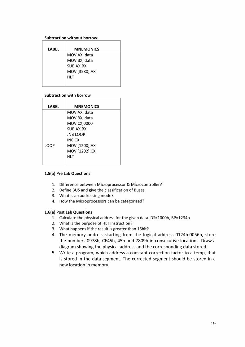
Subtraction without borrow:
LABEL
MNEMONICS
MOV AX, data MOV BX, data SUB AX,BX MOV [3580],AX HLT
Subtraction with borrow
LABEL
MNEMONICS
LOOP
MOV AX, data MOV BX, data MOV CX,0000 SUB AX,BX JNB LOOP INC CX MOV [1200],AX MOV [1202],CX HLT
1.5(a) Pre Lab Questions
1. Difference between Microprocessor & Microcontroller? 2. Define BUS and give the classification of Buses 3. What is an addressing mode? 4. How the Microprocessors can be categorized?
1.6(a) Post Lab Questions
1. Calculate the physical address for the given data. DS=1000h, BP=1234h 2. What is the purpose of HLT instruction? 3. What happens if the result is greater than 16bit? 4. The memory address starting from the logical address 0124h:0056h, store
the numbers 0978h, CE45h, 45h and 7809h in consecutive locations. Draw a diagram showing the physical address and the corresponding data stored.
5. Write a program, which address a constant correction factor to a temp, that is stored in the data segment. The corrected segment should be stored in a new location in memory.

20
Ex.No:1‐B (Multiplication and Division)
1.1.(b)Introduction
The purpose of this experiment is to learn about the registers, instruction sets, and arithmetic operators of 8086 by multiplication and division of the given two 16 bit numbers and store them in a memory location.
1.2 (b) Hardware Requirement
The 8086 Microprocessor kit, Power Supply.
1.3(b) Program Logic
The 8086 Processor provides both signed and unsigned multiply in their instruction set to overcome the loss of efficiency in performing the repeated addition.
The MUL instruction can have both 16 and 8 bit operands and the multiplicand is AX or AL, accordingly the result for a byte multiply is a 16 bit number in AX while that for a word multiply is a 32 bit number, the lower word of which is in AX and the higher word in DX.
1.4(b) Program
Introduction of general purpose registers, arithmetic operators (mul & div), direct addressing:
Multiplication:
LABEL
MNEMONICS
MOV AX,[1100] MOV BX,[1102] MUL BX MOV [1200],AX MOV [1202],DX HLT
Division:
LABEL
MNEMONICS
MOV AX,[1100] MOV BX,[1102] DIV BX MOV [1200],AX MOV [1202],DX HLT
21
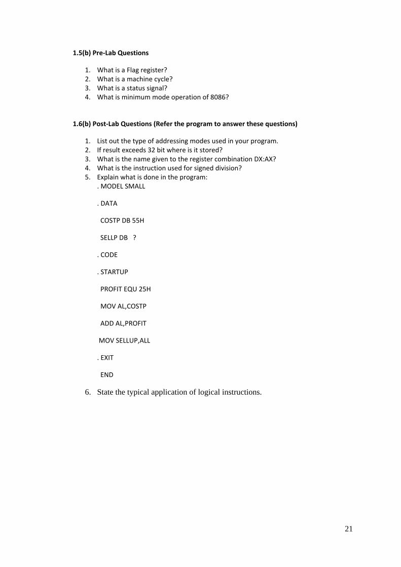
1.5(b) Pre‐Lab Questions
1. What is a Flag register? 2. What is a machine cycle? 3. What is a status signal? 4. What is minimum mode operation of 8086?
1.6(b) Post‐Lab Questions (Refer the program to answer these questions)
1. List out the type of addressing modes used in your program. 2. If result exceeds 32 bit where is it stored? 3. What is the name given to the register combination DX:AX? 4. What is the instruction used for signed division? 5. Explain what is done in the program:
. MODEL SMALL
. DATA
COSTP DB 55H
SELLP DB ?
. CODE
. STARTUP
PROFIT EQU 25H
MOV AL,COSTP
ADD AL,PROFIT
MOV SELLUP,ALL
. EXIT
END
6. State the typical application of logical instructions.

22
Lab 2
Ex.No.2: Introduction to General purpose registers, addressing modes,
logical operators of 8086
2.1 Introduction:
The purpose of this experiment is to learn about the general purpose registers, instruction sets, addressing modes and logical operators of 8086 by finding the larger and the smaller numbers from an array which is stored in a memory location.
2.2 Hardware Requirement: The 8086 Microprocessor kit, Power Supply. 2.3 Program Logic:
To find the largest number in any given array, the contents of the array must be compared with an arbitrary biggest number. The first number of the array is taken in a register AL. The second number of the array is compared with the first one. If the first one is greater than the second one, it is left unchanged. However if the second one is greater than the first, the second number replaces the first one in the AL register. The procedure is repeated for every number in the array and thus it requires n iterations. At the end of nth iteration the largest number will reside in the register AL. For smallest number the above said logic is repeated but, If the first number is smaller than the second one it is left unchanged. Otherwise the second number replaces the first number in the AL register 2.4 Program:
Introduction of general purpose registers, logical operators, indirect addressing, and loop instructions : Smallest number:
LABEL
MNEMONICS
LOOP1 LOOP2
MOV SI,1100 MOV CL,[SI] INC SI MOV AL,[SI] DEC CL INC SI MOV BL,[SI] CMP AL,BL JC LOOP2 MOV AL,BL DEC CL JNZ LOOP1 MOV [1200],AL HLT

23
Largest number:
LABEL
MNEMONICS
LOOP1 LOOP2
MOV SI,1100 MOV CL,[SI] INC SI MOV AL,[SI] DEC CL INC SI MOV BL,[SI] CMP AL,BL JNC LOOP2 MOV AL,BL DEC CL JNZ LOOP1 MOV [1200],AL HLT
2.5 Pre‐Lab Questions:
1. Draw the flowchart to find the largest and smallest number of an array? 2. What is the similarity and difference between Subtract and Compare Instruction? 3. What are the addressing modes are used in our program? 4. Initialize register CX to value FFFF and register AX to value 0000, write a program to
exchange the contents of both these register? 2.6 Post‐Lab Questions:
1. What is the purpose of MOV DS, AX? 2. What will be the status of flags after executing the program? 3. What are the addressing modes are used in our program? 4. What is the difference between JUMP and LOOP instructions? 5. Write a program to find the factorial of a number N. for 8086, the maximum size of
an operand for multiplication is only a word. This places a limitation on the value of N that can be used. Hence the value of N is to be less than 9. Store the result in memory.
6. Find the values in the destination for each line of this program . STC MOV AX,5432H RCR AL, 1 MOV CL,03 RCL AX,CL MOV CL,05 ROR AX,CL ROL AX,1 END
24
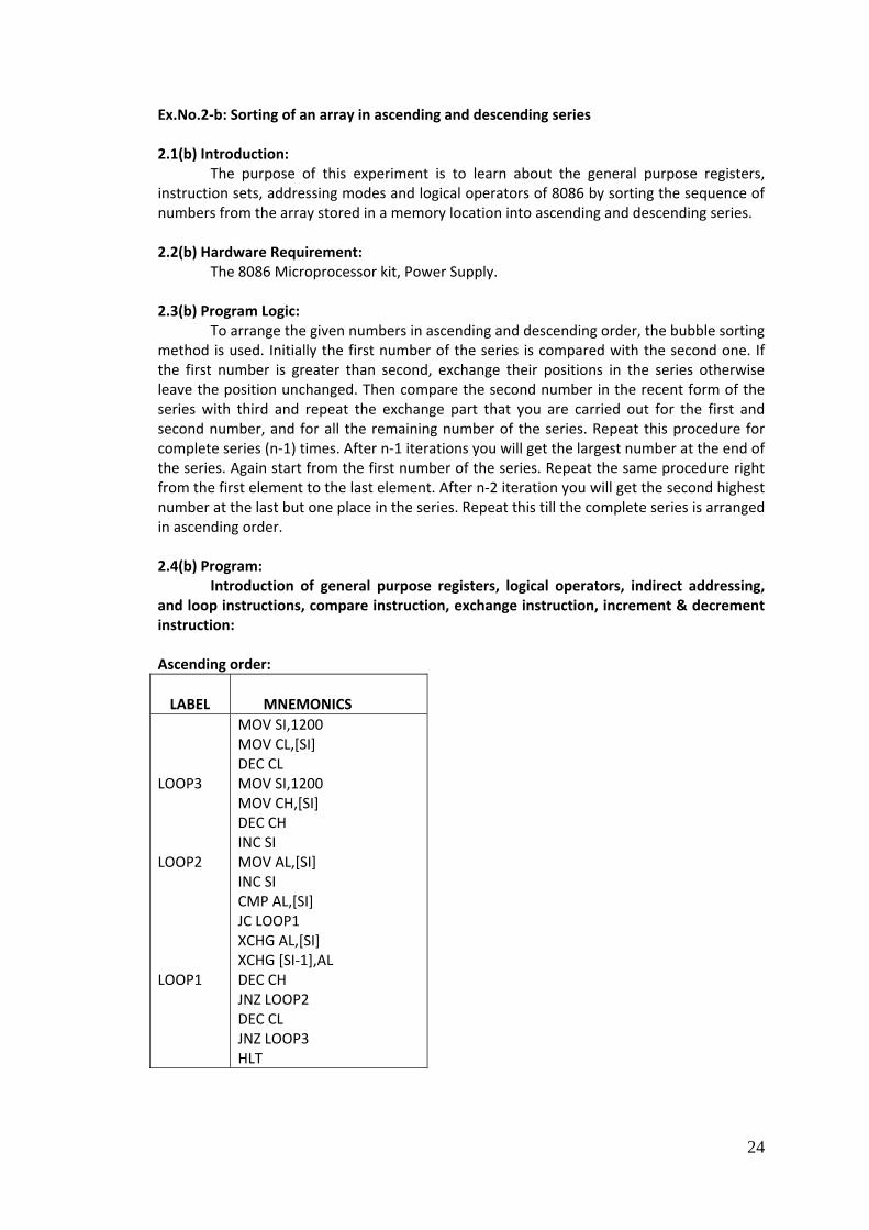
Ex.No.2‐b: Sorting of an array in ascending and descending series 2.1(b) Introduction:
The purpose of this experiment is to learn about the general purpose registers, instruction sets, addressing modes and logical operators of 8086 by sorting the sequence of numbers from the array stored in a memory location into ascending and descending series. 2.2(b) Hardware Requirement: The 8086 Microprocessor kit, Power Supply. 2.3(b) Program Logic: To arrange the given numbers in ascending and descending order, the bubble sorting method is used. Initially the first number of the series is compared with the second one. If the first number is greater than second, exchange their positions in the series otherwise leave the position unchanged. Then compare the second number in the recent form of the series with third and repeat the exchange part that you are carried out for the first and second number, and for all the remaining number of the series. Repeat this procedure for complete series (n‐1) times. After n‐1 iterations you will get the largest number at the end of the series. Again start from the first number of the series. Repeat the same procedure right from the first element to the last element. After n‐2 iteration you will get the second highest number at the last but one place in the series. Repeat this till the complete series is arranged in ascending order. 2.4(b) Program:
Introduction of general purpose registers, logical operators, indirect addressing, and loop instructions, compare instruction, exchange instruction, increment & decrement instruction: Ascending order:
LABEL
MNEMONICS
LOOP3 LOOP2 LOOP1
MOV SI,1200 MOV CL,[SI] DEC CL MOV SI,1200 MOV CH,[SI] DEC CH INC SI MOV AL,[SI] INC SI CMP AL,[SI] JC LOOP1 XCHG AL,[SI] XCHG [SI‐1],AL DEC CH JNZ LOOP2 DEC CL JNZ LOOP3 HLT

25
Descending order:
LABEL
MNEMONICS
LOOP3 LOOP2 LOOP1
MOV SI,1200 MOV CL,[SI] DEC CL MOV SI,1200 MOV CH,[SI] DEC CH INC SI MOV AL,[SI] INC SI CMP AL,[SI] JNC LOOP1 XCHG AL,[SI] XCHG [SI‐1],AL DEC CH JNZ LOOP2 DEC CL JNZ LOOP3 HLT
2.5(b) Pre‐Lab Questions:
1. Draw the flow chart to arrange a given series of numbers in ascending and descending order.
2. Write a small program using DAA instruction?
3. Which type of jump instruction (short, near or far) assembles for the following:
If the distance is 0210H bytes
If the distance is 0020H bytes
If the distance is 100000H bytes
2.6(b) Post‐Lab Questions:
1. What is the purpose of XCHG instruction?
2. What is the use of PUSH and POP instruction?
3. Write an assembly language program in 8086 to sort the given array of 16‐bit numbers in descending order.
4. What do square brackets means when they appear in an operand?
5. In a given program how many times DEC and JNZ instructions are executed? What will be content in AX register after executing the program?
MOV AX, 00FF
MOV CL, 05
REPEAT: INC AX

26
DEC CL
JNZ REPEAT
6. Explain what is done in this program. Assume sp – 0310h, when the stack was initialized. .MODEL SMALL .STACK 300H .CODE .STARTUP MOV AX, 4567H MOV BX, 0ACEH PUSH AX PUSH BX POP AX POP BX .EXIT END
27
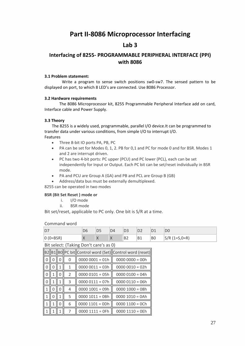
Part II‐8086 Microprocessor Interfacing Lab 3
Interfacing of 8255‐ PROGRAMMABLE PERIPHERAL INTERFACE (PPI) with 8086
3.1 Problem statement: Write a program to sense switch positions sw0‐sw7. The sensed pattern to be displayed on port, to which 8 LED’s are connected. Use 8086 Processor. 3.2 Hardware requirements The 8086 Microprocessor kit, 8255 Programmable Peripheral Interface add on card, Interface cable and Power Supply. 3.3 Theory
The 8255 is a widely used, programmable, parallel I/O device.It can be programmed to transfer data under various conditions, from simple I/O to interrupt I/O. Features
• Three 8‐bit IO ports PA, PB, PC • PA can be set for Modes 0, 1, 2. PB for 0,1 and PC for mode 0 and for BSR. Modes 1
and 2 are interrupt driven. • PC has two 4‐bit ports: PC upper (PCU) and PC lower (PCL), each can be set
independently for Input or Output. Each PC bit can be set/reset individually in BSR mode.
• PA and PCU are Group A (GA) and PB and PCL are Group B (GB) • Address/data bus must be externally demultiplexed.
8255 can be operated in two modes
BSR (Bit Set Reset ) mode or i. I/O mode ii. BSR mode
Bit set/reset, applicable to PC only. One bit is S/R at a time. Command word D7 D6 D5 D4 D3 D2 D1 D0
0 (0=BSR) X X X B2 B1 B0 S/R (1=S,0=R)
Bit select: (Taking Don't care's as 0) B2 B1 B0 PC bit Control word (Set) Control word (reset)
0 0 0 0 0000 0001 = 01h 0000 0000 = 00h
0 0 1 1 0000 0011 = 03h 0000 0010 = 02h
0 1 0 2 0000 0101 = 05h 0000 0100 = 04h
0 1 1 3 0000 0111 = 07h 0000 0110 = 06h
1 0 0 4 0000 1001 = 09h 0000 1000 = 08h
1 0 1 5 0000 1011 = 0Bh 0000 1010 = 0Ah
1 1 0 6 0000 1101 = 0Dh 0000 1100 = 0Ch
1 1 1 7 0000 1111 = 0Fh 0000 1110 = 0Eh
28
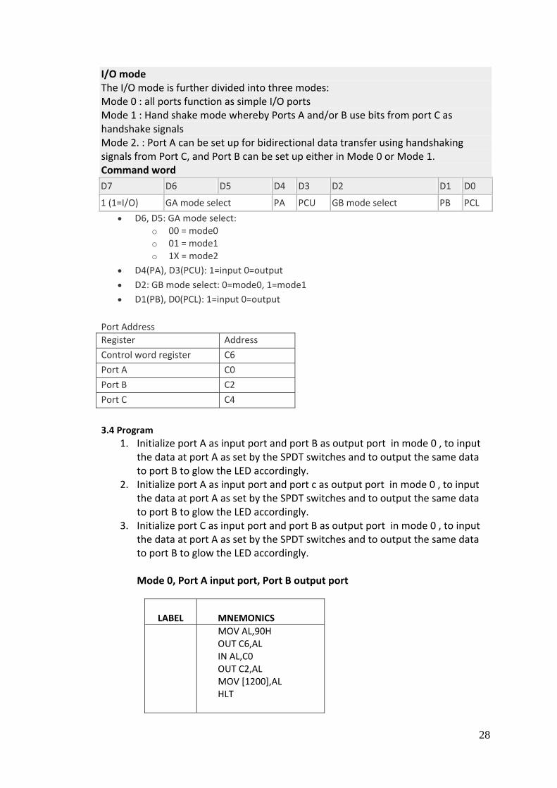
I/O mode The I/O mode is further divided into three modes: Mode 0 : all ports function as simple I/O ports Mode 1 : Hand shake mode whereby Ports A and/or B use bits from port C as handshake signals Mode 2. : Port A can be set up for bidirectional data transfer using handshaking signals from Port C, and Port B can be set up either in Mode 0 or Mode 1. Command word D7 D6 D5 D4 D3 D2 D1 D0
1 (1=I/O) GA mode select PA PCU GB mode select PB PCL • D6, D5: GA mode select:
o 00 = mode0 o 01 = mode1 o 1X = mode2
• D4(PA), D3(PCU): 1=input 0=output • D2: GB mode select: 0=mode0, 1=mode1 • D1(PB), D0(PCL): 1=input 0=output
Port Address Register Address Control word register C6 Port A C0 Port B C2 Port C C4
3.4 Program 1. Initialize port A as input port and port B as output port in mode 0 , to input
the data at port A as set by the SPDT switches and to output the same data to port B to glow the LED accordingly.
2. Initialize port A as input port and port c as output port in mode 0 , to input the data at port A as set by the SPDT switches and to output the same data to port B to glow the LED accordingly.
3. Initialize port C as input port and port B as output port in mode 0 , to input the data at port A as set by the SPDT switches and to output the same data to port B to glow the LED accordingly. Mode 0, Port A input port, Port B output port
LABEL
MNEMONICS
MOV AL,90H OUT C6,AL IN AL,C0 OUT C2,AL MOV [1200],AL HLT
29
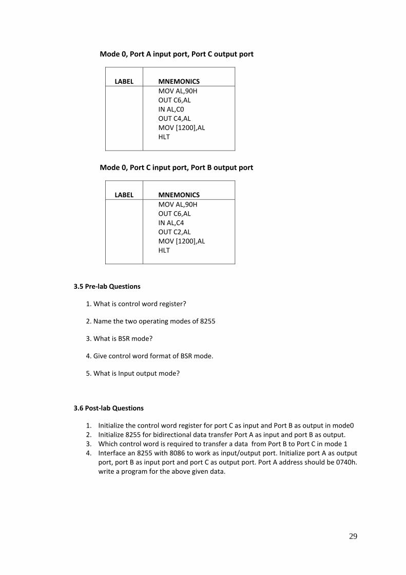
Mode 0, Port A input port, Port C output port
LABEL
MNEMONICS
MOV AL,90H OUT C6,AL IN AL,C0 OUT C4,AL MOV [1200],AL HLT
Mode 0, Port C input port, Port B output port
LABEL
MNEMONICS
MOV AL,90H OUT C6,AL IN AL,C4 OUT C2,AL MOV [1200],AL HLT
3.5 Pre‐lab Questions
1. What is control word register?
2. Name the two operating modes of 8255
3. What is BSR mode?
4. Give control word format of BSR mode.
5. What is Input output mode?
3.6 Post‐lab Questions
1. Initialize the control word register for port C as input and Port B as output in mode0 2. Initialize 8255 for bidirectional data transfer Port A as input and port B as output. 3. Which control word is required to transfer a data from Port B to Port C in mode 1 4. Interface an 8255 with 8086 to work as input/output port. Initialize port A as output
port, port B as input port and port C as output port. Port A address should be 0740h. write a program for the above given data.

30
Lab 4
Interfacing of 8279 Keyboard and display interface with 8086
processor.
4.1 Problem statement: Design a system to interface sixteen 7 segment display units. Write a program to
display the string in right entry mode. For example, first character will be displayed at the LSB position, then it will be shifted to the next left display and so on. After all the string displayed, the display should be blanked, then the same procedure repeated continuously.
4.2 Hardware requirements The 8051 Microcontroller kit, 8279 Interface add on card, Interface cable and Power Supply. 4.3 Theory
The 8279 is a widely used for debouncing keys, coding of the keypad matrix and refreshing the display elements in the microprocessor development system. Features A0: Selects data (0) or control/status (1) for reads and writes between micro and 8279. BD: Output that blanks the displays CLK: Used internally for timing. Max is 3 MHz. CN/ST: Control/strobe, connected to the control key on the keyboard CS: Chip select that enables programming, reading the keyboard, etc DB7 – DB0 : Consists of bidirectional pins that connect to data bus on microcontroller IRQ: Interrupt request, becomes 1 when a key is pressed, data is available. OUT A0‐ A3/B3‐B0: Outputs that sends data to the most significant/least significant nibble of display. RD(WR): Connects to micro's IORCor RDsignal, reads data/status registers. RESET: Connects to system RESET. R: Return lines are inputs used to sense key depression in the keyboard matrix. Shift: Shift connects to Shift key on keyboard. SL3 – SL0: Scan line outputs scan both the keyboard and displays.
Keyboard Interface of 8279 The keyboard matrix can be any size from 2x2 to 8x8. Pins SL2‐ SL0 sequentially scan
each column through a counting operation. The 74LS138 drives 0's on one line at a time. The 8279 scans RL pins synchronously with the scan.RL pins incorporate internal pull‐ups, no need for external resistor pull‐ups. Display mode set up:
0 0 0 D D K K K
31
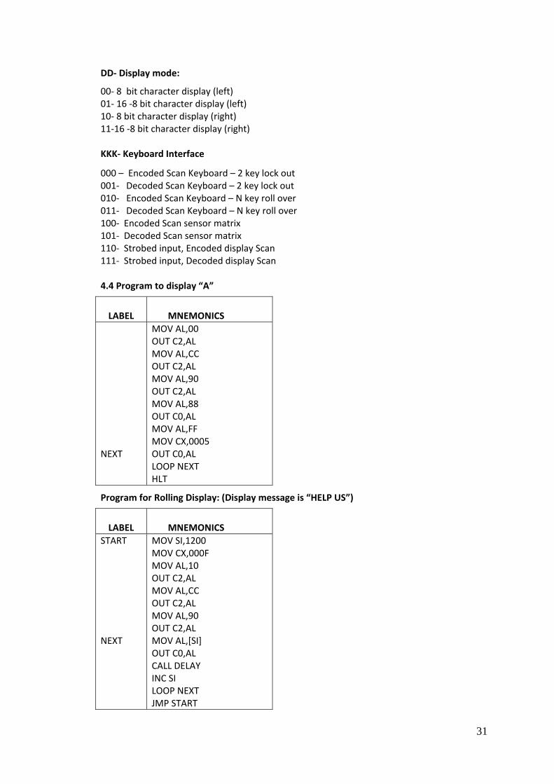
DD‐ Display mode:
00‐ 8 bit character display (left) 01‐ 16 ‐8 bit character display (left) 10‐ 8 bit character display (right) 11‐16 ‐8 bit character display (right) KKK‐ Keyboard Interface
000 – Encoded Scan Keyboard – 2 key lock out 001‐ Decoded Scan Keyboard – 2 key lock out 010‐ Encoded Scan Keyboard – N key roll over 011‐ Decoded Scan Keyboard – N key roll over 100‐ Encoded Scan sensor matrix 101‐ Decoded Scan sensor matrix 110‐ Strobed input, Encoded display Scan 111‐ Strobed input, Decoded display Scan 4.4 Program to display “A”
LABEL
MNEMONICS
NEXT
MOV AL,00 OUT C2,AL MOV AL,CC OUT C2,AL MOV AL,90 OUT C2,AL MOV AL,88 OUT C0,AL MOV AL,FF MOV CX,0005 OUT C0,AL LOOP NEXT HLT
Program for Rolling Display: (Display message is “HELP US”)
LABEL
MNEMONICS
START NEXT
MOV SI,1200 MOV CX,000F MOV AL,10 OUT C2,AL MOV AL,CC OUT C2,AL MOV AL,90 OUT C2,AL MOV AL,[SI] OUT C0,AL CALL DELAY INC SI LOOP NEXT JMP START

32
DELAY:
LABEL
MNEMONICS
DELAY LOOP1
MOV DX,A0FF DEC DX JNZ LOOP1 RET
4.5 PreLab:
1. State the operating modes of 8279
2. What are the use of CS, A0, RD and WR lines?
3. What is N key lock out?
4. What is N key roll over?
4.6 Post Lab:
1. Define Clock pre scaling.
2. What is BD?
3. Find the program clock command word if external clock frequency is 2MHz.
4. Interface an 8x8 matrix keyboard to 8086 through 8279 in 2 key lockout mode and write an assembly language program to read keycode to the pressed key. The external clock frequency is 2MHz. use input output mapped technique.

33
Lab 5
Ex.No.5: Introduction to registers, Instruction sets, arithmetic and
logical operators of 8051
5.1 Introduction:
The purpose of this experiment is to learn about the registers, instruction sets, and arithmetic operators, logical operators of 8051 by doing the BCD to HEXADECIMAL and vice versa of a given data using 8051 micro controller trainer kit.
5.2 Hardware Requirement: The 8051 Microcontroller kit, Power supply. 5.3 Program Logic:
In this program, 8 bit two digit Hexadecimal number system into BCD number system. The hexadecimal number system (also called base‐16) is a number system that uses 16 unique symbols to represent a particular value. Those symbols are 0‐9 and A‐F. 8 bit two digit BCD number system into Hexadecimal number system. Binary coded decimal (BCD) is a system of writing numerals that assigns a four‐digit binary code to each digit 0 through 9 in a decimal (base‐10) numeral. 5.4 Program:
Intoduction of DPTR, immediate addressing, logical, increment and swap instructions.
BCD to HEXADECIMAL:
LABEL
MNEMONICS
HERE
MOV DPTR,#4600 MOVX A,@DPTR MOV R5,A ANL A,#F0 SWAP A MOV R1,A MOV A,R5 ANL A,#0F MOV R2,A MOV A,R1 MOV B,#0A MUL AB ADD A,R2 INC DPTR MOVX @DPTR,A
SJMP HERE

34
Hexadecimal to BCD
LABEL
MNEMONICS
HERE
MOV DPTR,#4600 MOVX A,@DPTR MOV B,#64 DIV AB INC DPTR MOVX @DPTR,A MOV A,B MOV B,#0A DIV AB SWAP A ADD A,B INC DPTR MOVX @DPTR,A
SJMP HERE
5.4 Pre‐Lab Questions:
1. Upon reset, all ports of the 8051 are configured as _____________ (output, input). 2. Which ports of the 8051 have internal pull‐up resistors? 3. Which ports of the 8051 require the connection of external pull‐up resistors in order to be used for I/O? Show the drawing for the connection. 5.5 Post‐Lab Questions: 1. How the DPTR register is classified, explain its functions? 2. What is the function of EA pin in 8051? 3. List out the special function registers in 8051. 4. Find the number of times the following loop is performed
MOV R6, #200 BACK: MOV R5, #100 HERE: DJNZ R5, HERE
DJNZ R6, BACK 5. Examine the following code then answer the following questions
A. Will it jump to NEXT? B. What is in A after CJNE instruction is executed
MOV A, #55H CJNE A, #99H, NEXT

35
Lab 6
Ex.No.6: Introduction to General purpose registers, addressing modes,
logical operators of 8051
6.1 Introduction: The purpose of this experiment is to learn about the registers, instruction sets, and
arithmetic operators, logical operators of 8051 by doing the ASCII To Decimal and vice versa of a given data using 8051 micro controller trainer kit.
6.2 Hardware Requirement: The 8051 Microcontroller kit, Power supply. 6.3 Program Logic:
In this program, 8 bit two digit ASCII number system into decimal number system. Acronym for the American Standard Code for Information Interchange. Pronounced ask‐ee, ASCII is a code for representing English characters as numbers, with each letter assigned a number from 0 to 127 into decimal number and vice versa.
6.4 Program: Introduction of arithmetic, loop, registers of 8051
ASCII to DECIMAL:
LABEL
MNEMONICS STR LOOP HERE
MOV DPTR,#4500 MOV A,#DATA CLR C SUBB A,#30 CLR C SUBB A,#0A JC STR MOV A,#0FF SJMP LOOP ADD A,#0A MOVX @DPTR,A
SJMP HERE
DECIMAL TO ASCII:
LABEL
MNEMONICS
HERE
MOV DPTR,#4500MOVX A,@DPTR MOV R0,#30 ADD A,R0 INC DPTR MOVX @DPTR,A SJMP HERE
36
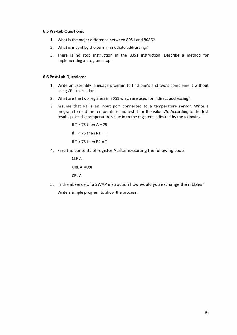
6.5 Pre‐Lab Questions:
1. What is the major difference between 8051 and 8086?
2. What is meant by the term immediate addressing?
3. There is no stop instruction in the 8051 instruction. Describe a method for implementing a program stop.
6.6 Post‐Lab Questions:
1. Write an assembly language program to find one’s and two’s complement without using CPL instruction.
2. What are the two registers in 8051 which are used for indirect addressing?
3. Assume that P1 is an input port connected to a temperature sensor. Write a program to read the temperature and test it for the value 75. According to the test results place the temperature value in to the registers indicated by the following.
If T = 75 then A = 75
If T < 75 then R1 = T
If T > 75 then R2 = T
4. Find the contents of register A after executing the following code
CLR A
ORL A, #99H
CPL A
5. In the absence of a SWAP instruction how would you exchange the nibbles?
Write a simple program to show the process.

37
Ex.No.6 (b): Square Root Of A Given Data
6.1(b) Introduction:
The purpose of this experiment is to learn about the registers, instruction sets, and
arithmetic operators, logical operators, addressing modes of 8051 by doing the Square root
of a given data using 8051 micro controller trainer kit.
6.2 (b) Hardware Requirement: The 8051 Microcontroller kit , Power supply.
6.3(b) Program Logic: In this program, the square root of a number can be found out by division and subtraction method.
6.4(b) Program:
LABEL
MNEMONICS
LOOP RESULT HERE
MOV DPTR,#5600
MOVX A,@DPTR
MOV R1,A
MOV R2,#01
MOV A,R1
MOV B,R2
DIV AB
MOV R3,A
MOV R4,B
SUBB A,R2
JZ RESULT
INC R2
SJMP LOOP
MOV DPTR,#5700
MOV A,R3
MOVX @DPTR,A
SJMP HERE
38
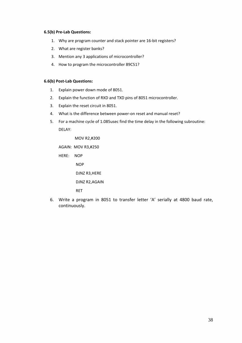
6.5(b) Pre‐Lab Questions:
1. Why are program counter and stack pointer are 16‐bit registers?
2. What are register banks?
3. Mention any 3 applications of microcontroller?
4. How to program the microcontroller 89C51?
6.6(b) Post‐Lab Questions:
1. Explain power down mode of 8051.
2. Explain the function of RXD and TXD pins of 8051 microcontroller.
3. Explain the reset circuit in 8051.
4. What is the difference between power‐on reset and manual reset?
5. For a machine cycle of 1.085usec find the time delay in the following subroutine:
DELAY:
MOV R2,#200
AGAIN: MOV R3,#250
HERE: NOP
NOP
DJNZ R3,HERE
DJNZ R2,AGAIN
RET
6. Write a program in 8051 to transfer letter ‘A’ serially at 4800 baud rate, continuously.

39
Lab 7
Interfacing of 8254 programmable timer interface with 8051
Microcontroller.
7.1 Problem Statement: Write a program to generate waveform that has 50% duty cycle of 150KHz. Assume
that system clock available is 1.5MHz. Implement using 8051 Microcontroller. 7.2 Hardware requirements The 8051Microcontroller kit, 8253 Interface add on card, Interface cable and Power Supply. 7.3 Theory
The main features of 8253 are as follows: 1. Three independent 16 bit counters 2. Input clock 3. Programmable counter modes The clk0 can be connected either to the pclk or to the debounce circuit. Using the debounce circuit we can generate a pulse and clock the timer. Similarly clock1 can be connected to pclk and clock2 can be connected to either pclk or out0. In a microprocessor based application, interrupting the processor after a time delay is essential which is achieved using a timer.
7.3. 1 MODES Mode 0 – Interrupt on terminal count The output will be initially low after mode set operation. After loading the counter, the output will remain low while counting and on terminal count the output will become high, until reloaded again. Channel 0 is in mode 0 and the program is executed. Output is observed through a CRO.
Mode 1 – Programmable one shot
After loading the counter, the output will remain low following the rising edge of the gate input. The output will go high on the terminal count. It is retriggerable, hence the output will remain low for the full count after the rising edge of the gate input. Execute the program, give the clock pulses through the debounce logic and observe the output at the CRO.
Mode 2 – Rate generator
It is a divide by N counter. The output will be low for for one period of the clock input. The period from one output pulse to the next equals the number of input counts in the count register. In the CRO observe the input at channel 1 and the output at out1.
Mode 3 – Square Wave Generator
It is similar to mode 2 except that the output will remain high for one half of the count and go low for the other half for even number count. If the count is odd, the output will remain high for (count‐1)/2 counts.
40
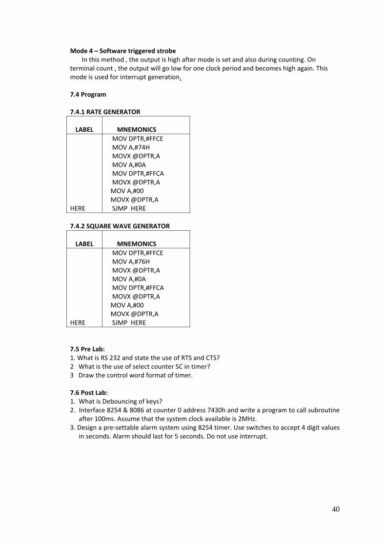
Mode 4 – Software triggered strobe In this method , the output is high after mode is set and also during counting. On
terminal count , the output will go low for one clock period and becomes high again. This mode is used for interrupt generation. 7.4 Program 7.4.1 RATE GENERATOR
LABEL
MNEMONICS
HERE
MOV DPTR,#FFCE MOV A,#74H MOVX @DPTR,A MOV A,#0A MOV DPTR,#FFCA MOVX @DPTR,A MOV A,#00 MOVX @DPTR,A SJMP HERE
7.4.2 SQUARE WAVE GENERATOR
LABEL
MNEMONICS
HERE
MOV DPTR,#FFCE MOV A,#76H MOVX @DPTR,A MOV A,#0A MOV DPTR,#FFCA MOVX @DPTR,A MOV A,#00 MOVX @DPTR,A SJMP HERE
7.5 Pre Lab: 1. What is RS 232 and state the use of RTS and CTS? 2 What is the use of select counter SC in timer? 3 Draw the control word format of timer. 7.6 Post Lab: 1. What is Debouncing of keys? 2. Interface 8254 & 8086 at counter 0 address 7430h and write a program to call subroutine
after 100ms. Assume that the system clock available is 2MHz. 3. Design a pre‐settable alarm system using 8254 timer. Use switches to accept 4 digit values
in seconds. Alarm should last for 5 seconds. Do not use interrupt.

41
Lab 8
Ex.No.8: Interfacing of Stepper motor with 8051 Microcontroller.
8.1 Problem Statement: Write an ALP to trigger a stepper motor with +5V, at an angle of 15 degree in each
step in both clockwise and anticlockwise with same speed and different speeds. Implement using 8051 Microcontroller. 8.2 Hardware Requirement: The 8051 Microcontroller kit, Stepper motor interface add on card, interface cable, Power Supply. 8.3 Program Logic:
A motor in which the rotor is able to assume only discrete stationary angular position is a stepper motor. The rotor motion occurs in a stepwise manner from one equilibrium position to the next. They are widely used in open and closed looped systems in a variety of applications. It is either of reluctance type or permanent magnet type. The four poles structure is continuous with the stator frame and the magnetic field passes through the cylindrical stator annular ring. The stator poles and three pairs of rotor poles, there exists 12 possible positions in which a south pole of the rotor can lock with the north pole of the stator. From this it can be noted that the step size is 360( in degrees)/ Ns x Nr where Ns = number of stator poles Nr = number of pair of rotor poles.
There are three different stepping schemes for a stepper motor. 1. Wave scheme 2. 2‐ phase scheme 3. half stepping and mixed scheme
8.3.1 Wave scheme The stepper motor windings A1,A2,B1,B2 can be cyclically excited with a DC current
to run the motor in the clockwise direction. Consider the four rotor positions of the motor along with the stator excitations. The switching scheme for the wave mode excitation is given as follows.
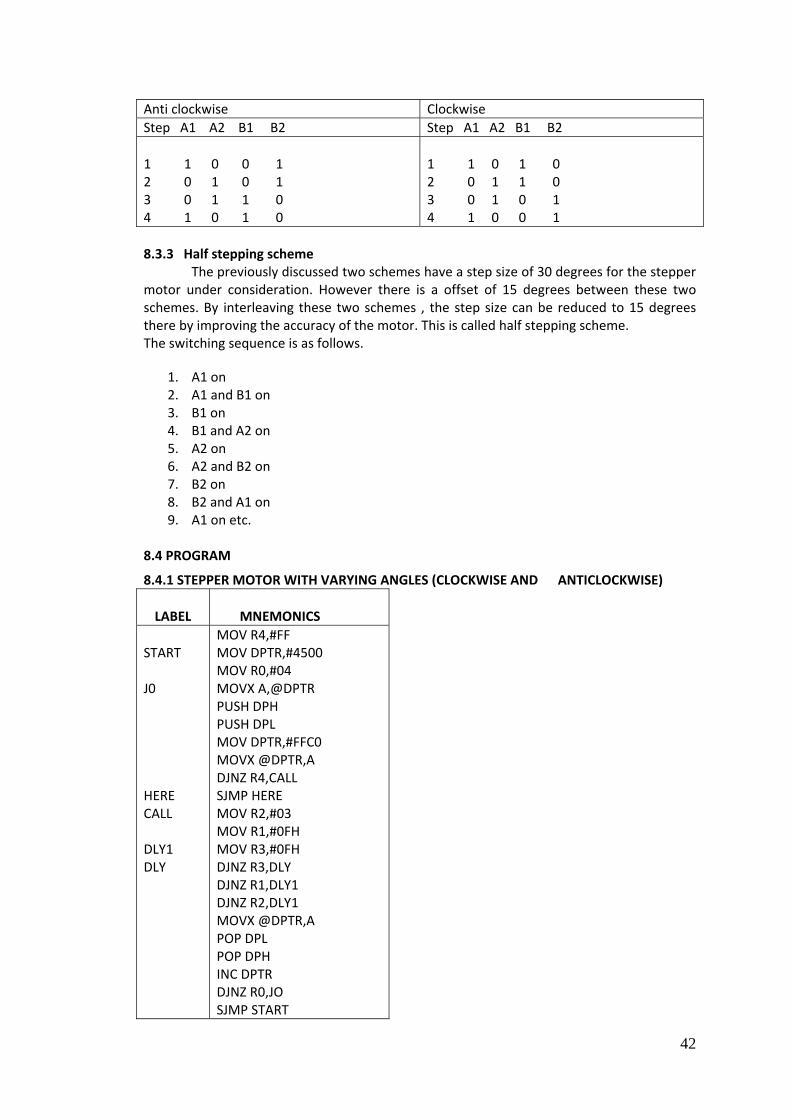
8.3.2 2‐ Phase scheme:
In this scheme the two adjacent stator windings are energized. There are two magnetic fields achieved in quadrature and none of the rotor pole faces can be in a direct alignment with the stator poles. The switching scheme for the 2‐ phase mode excitation is given as follows.
Anti clockwise Clockwise Step A1 A2 B1 B2 Step A1 A2 B1 B2 1 1 0 0 0 2 0 0 0 1 3 0 1 0 0 4 0 0 1 0
1 1 0 0 0 2 0 0 1 0 3 0 1 0 0 4 0 0 0 1
42
8.3.3 Half stepping scheme
The previously discussed two schemes have a step size of 30 degrees for the stepper motor under consideration. However there is a offset of 15 degrees between these two schemes. By interleaving these two schemes , the step size can be reduced to 15 degrees there by improving the accuracy of the motor. This is called half stepping scheme. The switching sequence is as follows.
1. A1 on 2. A1 and B1 on 3. B1 on 4. B1 and A2 on 5. A2 on 6. A2 and B2 on 7. B2 on 8. B2 and A1 on 9. A1 on etc.
8.4 PROGRAM
8.4.1 STEPPER MOTOR WITH VARYING ANGLES (CLOCKWISE AND ANTICLOCKWISE)
LABEL
MNEMONICS START J0 HERE CALL DLY1 DLY
MOV R4,#FF MOV DPTR,#4500 MOV R0,#04 MOVX A,@DPTR PUSH DPH PUSH DPL MOV DPTR,#FFC0 MOVX @DPTR,A DJNZ R4,CALL SJMP HERE MOV R2,#03 MOV R1,#0FH MOV R3,#0FH DJNZ R3,DLY DJNZ R1,DLY1 DJNZ R2,DLY1 MOVX @DPTR,A POP DPL POP DPH INC DPTR DJNZ R0,JO SJMP START
Anti clockwise Clockwise Step A1 A2 B1 B2 Step A1 A2 B1 B2 1 1 0 0 1 2 0 1 0 1 3 0 1 1 0 4 1 0 1 0
1 1 0 1 0 2 0 1 1 0 3 0 1 0 1 4 1 0 0 1
43
8.4.2 STEPPER MOTOR WITH VARIABLE SPEED
LABEL
MNEMONICS
START J0 DLY1 DLY
MOV DPTR,#4500 MOV R0,#04 MOVX A,@DPTR PUSH DPH PUSH DPL MOV DPTR,#FFC0 MOV R2,#04H MOV R1,#0FH MOV R3,#0FH DJNZ R3,DLY DJNZ R1,DLY1 DJNZ R2,DLY1 MOVX @DPTR,A POP DPL POP DPH INC DPTR DJNZ R0,JO SJMP START
8.5 Pre‐Lab Questions: 1 State applications of stepper motor in control systems 2 Draw the 4 possible rotor positions and the corresponding stator excitations in a
stepper motor 3 What is the specific property of the stepper motor which makes it compatible to
interface with the processor? 4. Can a single phase motor or a DC motor be interfaced with a 8086 processor? 5 What is the operating voltage of a stepper motor? 6 What are the different types of stepper motor? 7 State any two applications of stepper motor interfaced with 8086.
8.6 Post Lab: 1. Write a program to run the stepper motor for any number of steps and to stop it. 2. Justify the look up table listed in your program. 3. What do you mean by the instruction out C0 in the program? 4. What is the value of the delay element used in the program? 5. Write a program to interface the stepper motor with 8051 and make it run in
clockwise and anti clock wise direction. 6. Write an ALP to control coveyor belt using stepper motor and 8051 controller. Belt
moves continuously at the rate of 1 step/sec, but stops for 5secs, when external interrupt occurs ant then continues to move.
7. Design a stepper motor controller and write an ALP to rotate shaft of a 4 phase stepper motor.
(i) in clockwise 5 rotations. (ii) in anticlockwise 5 rotations.
44
Part IV – Nuvoton Processor
Lab 9
Ex.No.9: Implementation of Seven segment display from “0000” to
“9999” using Nuvoton board.
9.1 Problem Statement: Write a program to display the number from 0000 to 9999. 4 LED’s that are in the Nuvoton Nu‐LB‐NUC140 series Board should be used to display the number sequence.
9.2 Tool Requirement: KEIL Uversion 4.0, Nuvoton CMSIS Library Files, DrvSYS Library Files, NUC140LB Series ARM Target Board. 9.3 Program :
Smpl_7seg : counting from 0 to 9999 and display on 7‐segment LEDs
#include <Stdio.h>
#include "NUC1xx.h"
#include "DrvSYS.h"
#include "Seven_Segment.h"
// display an integer on four 7‐segment LEDs
void seg_display(int16_t value)
{
int8_t digit;
digit = value / 1000;
close_seven_segment();
show_seven_segment(3,digit);
DrvSYS_Delay(5000);
value = value ‐ digit * 1000;
digit = value / 100;
close_seven_segment();
show_seven_segment(2,digit);
DrvSYS_Delay(5000);
value = value ‐ digit * 100;
digit = value / 10;
close_seven_segment();
show_seven_segment(1,digit);
DrvSYS_Delay(5000);

45
value = value ‐ digit * 10;
digit = value;
close_seven_segment();
show_seven_segment(0,digit);
DrvSYS_Delay(5000);
int32_t main (void)
{
int32_t i =0;
UNLOCKREG();
DrvSYS_Open(48000000);
LOCKREG();
while(i<0x10000)
{
seg_display(i); // display i on 7‐segment display
DrvSYS_Delay(20000); // delay for keeping display
i++; // increment i
}
}
9.4 Pre‐Lab Questions:
1. What is the processor used in Nuvoton board?
2. What is GPIO and where it is used?
3. Differentiate RISC and CISC machine.
9.5 Post‐Lab Questions:
1. How seven segment display is interfaced in Nuvoton series

46
Lab 10
Ex.No.10: Implementation of Seven segment display using ADC in
Nuvoton board.
10.1 Problem Statement:
Write a program to display the digital value obtained from inbuilt ADC in the 4 LED’s in the NuvotonNu‐LB‐NUC140 series Board. Assume that the clock source available is 22MHz and baud rate is 9600 bps.
10.2 Tool Requirement: KEIL Uversion 4.0, Nuvoton CMSIS Library Files, DrvSYS Library Files NUC140LB Series ARM Target Board.
10.3 Program :
/* Sample Code : Smpl_7seg_ADC7 */
/* input : ADC[7] (12‐bit) */
/* output : Four Digit on 7‐segment display */
#include <stdio.h>
#include "NUC1xx.h"
#include "Seven_Segment.h"
#define BAUDRATE 9600
void InitADC (void)
{
/* Step 1. GPIO initial */
GPIOA‐>OFFD|=0x00800000; //Disable digital input path
SYS‐>GPAMFP.ADC7_SS21_AD6=1; //Set ADC function
/* Step 2. Enable and Select ADC clock source, and then enable ADC module */
SYSCLK‐>CLKSEL1.ADC_S = 2; //Select 22Mhz for ADC
SYSCLK‐>CLKDIV.ADC_N = 1; //ADC clock source = 22Mhz/2 =11Mhz;
SYSCLK‐>APBCLK.ADC_EN = 1; //Enable clock source
ADC‐>ADCR.ADEN = 1; //Enable ADC module
/* Step 3. Select Operation mode */
ADC‐>ADCR.DIFFEN = 0; //single end input
ADC‐>ADCR.ADMD = 0; //single mode
/* Step 4. Select ADC channel */
ADC‐>ADCHER.CHEN = 0x80;
47
/* Step 5. Enable ADC interrupt */
ADC‐>ADSR.ADF =1; //clear the A/D interrupt flags for safe
ADC‐>ADCR.ADIE = 1;
// NVIC_EnableIRQ(ADC_IRQn);
/* Step 6. Enable WDT module */
ADC‐>ADCR.ADST=1;
}
void Delay(int32_t count)
{
while(count‐‐)
{
// __NOP;
}
}
void seg_display(int16_t value)
{
int8_t digit;
digit = value / 1000;
close_seven_segment();
show_seven_segment(3,digit);
Delay(5000);
value = value ‐ digit * 1000;
digit = value / 100;
close_seven_segment();
show_seven_segment(2,digit);
Delay(5000);
value = value ‐ digit * 100;
digit = value / 10;
close_seven_segment();
show_seven_segment(1,digit);
Delay(5000);
value = value ‐ digit * 10;
digit = value;
close_seven_segment();
show_seven_segment(0,digit);
48
Delay(5000);
}
/*‐‐‐‐‐‐‐‐‐‐‐‐‐‐‐‐‐‐‐‐‐‐‐‐‐‐‐‐‐‐‐‐‐‐‐‐‐‐‐‐‐‐‐‐‐‐‐‐‐‐‐‐‐‐‐‐‐‐‐‐‐‐‐‐‐‐‐‐‐‐‐‐‐‐‐‐
MAIN function
‐‐‐‐‐‐‐‐‐‐‐‐‐‐‐‐‐‐‐‐‐‐‐‐‐‐‐‐‐‐‐‐‐‐‐‐‐‐‐‐‐‐‐‐‐‐‐‐‐‐‐‐‐‐‐‐‐‐‐‐‐‐‐‐‐‐‐‐‐‐‐‐‐‐‐‐*/
int32_t main (void)
{
int32_t adc_value;
UNLOCKREG();
SYSCLK‐>PWRCON.XTL12M_EN = 1; //Enable 12Mhz and set HCLK‐>12Mhz
SYSCLK‐>CLKSEL0.HCLK_S = 0;
LOCKREG();
InitADC();
while(1)
{
while (ADC‐>ADSR.ADF==0); // ADC Flag, wait till 1 (A/DC conversion done)
ADC‐>ADSR.ADF=1; // write 1 to ADF is to clear the flag
adc_value=ADC‐>ADDR[7].RSLT; // input 12‐bit ADC value
seg_display(adc_value); // display value to 7‐segment display
ADC‐>ADCR.ADST=1; // activate next ADC sample
// 1 : conversion start; // 0 : conversion stopped, ADC enter idle state
}
}
10.4 Pre Lab Questions:
1.What does ARM mean?
2. State the specifications of the Nuvoton processor?
3. Differentiate Nuvoton and 8086 trainer boards
10.5 Post Lab Questions
1. What is IDE and why it is needed?
2. What is meant by in circuit programming?
3. Interface an ADC0804 with a processor, for the speech data is converted into digital data. This data is stored in the array at sampling rate of 1/2048 of second. Then the sampled data is sent to DAC0830 with same rate to reduce the speech signal.
49
Lab 11
Implementation of UART using Nuvoton board.
11.1 Problem Statement: Design a suitable mechanism in the NuvotonNu‐LB‐NUC140 series Board for full duplex communication, for the baud rate of 9600 bps, 8 data bits, 1 stop bit and 0 parity bit.
11.2 Tool Requirement: KEIL Uversion 4.0, Nuvoton CMSIS Library Files, DrvSYS Library Files NUC140LB Series ARM Target Board. 11.3 Program:
//
// Smpl_UART0
//
// Nu‐LB‐NUC140
// pin32 GPB0/RX0 to another board's UART TX
// pin33 GPB1/TX0 to another board's UART RX
#include <stdio.h>
#include "Driver\DrvUART.h"
#include "Driver\DrvGPIO.h"
#include "Driver\DrvSYS.h"
#include "NUC1xx.h"
#include "NUC1xx‐LB_002\LCD_Driver.h"
volatile uint8_t comRbuf[16] ={0x30};
volatile uint16_t comRbytes = 0;
volatile uint16_t comRhead = 0;
volatile uint16_t comRtail = 0;
char TEXT1[16] = "TX: sending... ";
char TEXT2[16] = "RX: ";
/*‐‐‐‐‐‐‐‐‐‐‐‐‐‐‐‐‐‐‐‐‐‐‐‐‐‐‐‐‐‐‐‐‐‐‐‐‐‐‐‐‐‐‐‐‐‐‐‐‐‐‐‐‐‐‐‐‐‐‐‐‐‐‐‐‐‐‐‐‐‐‐‐‐‐‐‐‐‐‐‐‐‐‐‐‐‐‐‐‐‐‐‐‐‐‐‐‐‐‐‐‐‐‐‐‐*/
/* UART Callback function */
/*‐‐‐‐‐‐‐‐‐‐‐‐‐‐‐‐‐‐‐‐‐‐‐‐‐‐‐‐‐‐‐‐‐‐‐‐‐‐‐‐‐‐‐‐‐‐‐‐‐‐‐‐‐‐‐‐‐‐‐‐‐‐‐‐‐‐‐‐‐‐‐‐‐‐‐‐‐‐‐‐‐‐‐‐‐‐‐‐‐‐‐‐‐‐‐‐‐‐‐‐‐‐‐‐‐*/
void UART_INT_HANDLE(void)
50
{
uint8_t i;
uint8_t bInChar[1] = {0xFF};
while(UART0‐>ISR.RDA_IF==1)
{
DrvUART_Read(UART_PORT0,bInChar,1);
if(comRbytes < 8) // check if Buffer is full
{
comRbuf[comRbytes] = bInChar[0];
comRbytes++;
}
else if (comRbytes==8)
{
comRbytes=0;
sprintf(TEXT2+4,"%s",comRbuf);
print_lcd(2,TEXT2);
}
}
}
int32_t main()
{
uint8_t i =0;
uint8_t dataout[8] = "NuMicro0";
STR_UART_T sParam;
UNLOCKREG();
DrvSYS_Open(48000000);
LOCKREG();
Initial_panel();
clr_all_panel();
print_lcd(0,"Smpl_UART0 ");
/* Set UART Pin */
51
DrvGPIO_InitFunction(E_FUNC_UART0);
/* UART Setting */
sParam.u32BaudRate = 9600;
sParam.u8cDataBits = DRVUART_DATABITS_8;
sParam.u8cStopBits = DRVUART_STOPBITS_1;
sParam.u8cParity = DRVUART_PARITY_NONE;
sParam.u8cRxTriggerLevel= DRVUART_FIFO_1BYTES;
/* Set UART Configuration */
if(DrvUART_Open(UART_PORT0,&sParam) != E_SUCCESS);
DrvUART_EnableInt(UART_PORT0, DRVUART_RDAINT, UART_INT_HANDLE);
while(1)
{
dataout[7] = 0x30 +i;
DrvUART_Write(UART_PORT0, dataout,8);
i++;
if (i>=10) i = 0;
sprintf(TEXT1+14,"%d",i);
print_lcd(1,TEXT1);
DrvSYS_Delay(5000000);
}
//DrvUART_Close(UART_PORT0);
}
11.4 Pre lab:
1. What is meant by UART?
2. State applications of UART.
3. What is a sample and hold circuit?
11.5 Post lab:
1. Write a program to receive a one character for the baud rate 110bps, data bits are
8, stop bit is 1 and parity bit is none.
52
Lab 11
Implementation of temperature sensor using Nuvoton board.
12.1 Problem Statement: Design a temperature sensor (thermistor) for 25 degree in the NuvotonNu‐LB‐
NUC140 series Board. Assume that the clock source available is 22MHz and baud rate is 9600 bps.
12.2 Tool Requirement: KEIL Uversion 4.0, Nuvoton CMSIS Library Files, DrvSYS Library Files NUC140LB Series ARM Target Board. 12.3 Program:
//
// Smpl_ADC_Thermistor : Thermistor
//
// use ADC6 to read Thermistor resistance
// pin GPA6 : ADC6
// resistance = temperature
// NTSA0103JZ100
// R = 10K ohm at 25 degree
// R = 3.496 K ohm at 50 degree
#include <stdio.h>
#include "NUC1xx.h"
#include "LCD_Driver.h"
void InitADC(void)
{
/* Step 1. GPIO initial */
GPIOA‐>OFFD|=0x00800000; //Disable digital input path
SYS‐>GPAMFP.ADC6_AD7=1; //Set ADC function

53
/* Step 2. Enable and Select ADC clock source, and then enable ADC module */
SYSCLK‐>CLKSEL1.ADC_S = 2; //Select 22Mhz for ADC
SYSCLK‐>CLKDIV.ADC_N = 1; //ADC clock source = 22Mhz/2 =11Mhz;
SYSCLK‐>APBCLK.ADC_EN = 1; //Enable clock source
ADC‐>ADCR.ADEN = 1; //Enable ADC module
/* Step 3. Select Operation mode */
ADC‐>ADCR.DIFFEN = 0; //single end input
ADC‐>ADCR.ADMD = 0; //single mode
/* Step 4. Select ADC channel */
ADC‐>ADCHER.CHEN = 0x40; // channel bit [7:0]
/* Step 5. Enable ADC interrupt */
ADC‐>ADSR.ADF =1; //clear the A/D interrupt flags for safe
ADC‐>ADCR.ADIE = 1;
// NVIC_EnableIRQ(ADC_IRQn);
/* Step 6. Enable WDT module */
ADC‐>ADCR.ADST=1;
}
void Delay(int count)
{
while(count‐‐);
}
int32_t main (void)
{
uint32_t R = 9950; // pullup resister
uint32_t r; // thermister
uint32_t adc_value;
uint32_t temp;
char TEXT0[16]="ADC6 ‐Thermistor";
char TEXT1[16]="ADC : ";
char TEXT2[16]="r : ohm";

54
char TEXT3[16]="Temp.: .C";
UNLOCKREG();
SYSCLK‐>PWRCON.XTL12M_EN = 1; //Enable 12Mhz and set HCLK‐>12Mhz
SYSCLK‐>CLKSEL0.HCLK_S = 0;
LOCKREG();
InitADC();
Initial_panel(); //call initial pannel function
clr_all_panel();
print_lcd(0,TEXT0);
print_lcd(1,TEXT1);
print_lcd(2,TEXT2);
print_lcd(3,TEXT3);
while(1)
{
while(ADC‐>ADSR.ADF==0);
ADC‐>ADSR.ADF=1;
adc_value = ADC‐>ADDR[6].RSLT & 0x0FFC;
r = R * (4096 ‐ adc_value) / adc_value;
// adc_value = 4096 * R / (R+r);
sprintf(TEXT1+7,"%d", adc_value);
print_lcd(1, TEXT1);
sprintf(TEXT2+7,"%d", r);
print_lcd(2, TEXT2);
temp = 0;
sprintf(TEXT3+7,"%s", "unknown");
print_lcd(3,TEXT3);

55
Delay(1000);
ADC‐>ADCR.ADST=1;
}
}
12.4 Pre lab:
1. Define thermistor. 2. What is meant by data acquisition?
12.5 Post lab:
1. Design a thermistor for temperature of 50 degree in the NuvotonNu‐LB‐NUC140 series Board. Assume that the clock source available is 22MHz and baud rate is 9600.
56
CODE COMPOSER STUDIO INTRODUCTION TO CODE COMPOSER STUDIO
Code Composer is the DSP industry's first fully integrated development environment
(IDE) with DSP‐specific functionality. With a familiar environment liked MS‐based
C++TM, Code Composer lets you edit, build, debug, profile and manage projects
from a single unified environment. Other unique features include graphical signal
analysis, injection/extraction of data signals via file I/O, multi‐processor debugging,
automated testing and customization via a C‐interpretive scripting language and
much more.
CODE COMPOSER FEATURES INCLUDE:
• IDE
• Debug IDE
• Advanced watch windows
• Integrated editor
• File I/O, Probe Points, and graphical algorithm scope probes
• Advanced graphical signal analysis
• Interactive profiling
• Automated testing and customization via scripting
• Visual project management system
• Compile in the background while editing and debugging
• Multi‐processor debugging
• Help on the target DSP
To create a system configuration using a standard configuration file:
Step 1: Start CCS Setup by double clicking on the Setup CCS desktop icon.
Step 2: select Family c67xx
Platform simulator
Endianness little
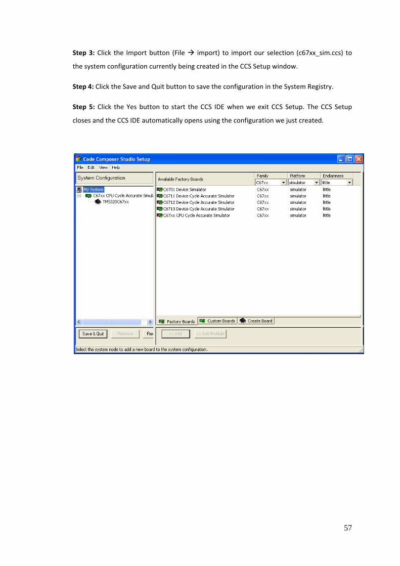
57
Step 3: Click the Import button (File import) to import our selection (c67xx_sim.ccs) to
the system configuration currently being created in the CCS Setup window.
Step 4: Click the Save and Quit button to save the configuration in the System Registry.
Step 5: Click the Yes button to start the CCS IDE when we exit CCS Setup. The CCS Setup
closes and the CCS IDE automatically opens using the configuration we just created.

58
PROCEDURE TO WORK ON CODE COMPOSER STUDIO
Step 1: Creating a New Project
From the Project menu, choose New.
In the Project Name field, type the name we want for our project. Each project we
create must have a unique name, and Click Finish. The CCS IDE creates a project file
called projectname.pjt. This file stores our project settings and references the
various files used by our project.
The Project Creation wizard window displays.
Step 2: Creating a source file
Create a new source file using ‘File new source file ‘ pull down menu and save
the source file with .c extension in the current project name directory.

59
Save as type: c/c++ source file (*.c*)
Path: C:\CCStudio_v3.1\ MyProjects\Project Name\
Step 3: Add files to our project (source file\ library file\ linker file)
Source file: Add the source file in the project using ‘Project add files to project’
pull down menu.
Files of type: c/c++ source file (*.c*)
Path: C:\CCStudio_v3.1\ MyProjects\Project Name\file_name.c
Library file: Add the library file in the project using ‘Project add files to project’
pull down menu.
Files of type: Object and Library Files (*.o*,*.l*)
Path: C:\CCStudio_v3.1\ C6000\ cgtools\ lib \ rts6700.lib
Linker file: Add the linker file in the project using ‘Project add files to project’
pull down menu.
Files of type: Linker command Files (*.cmd*,*.lcf*)
Path: C:\CCStudio_v3.1\ tutorial\ dsk6711\ hello1 \ hello.cmd
Step 4: Building and Running the Program (compile\ Build\ Load Program\ Run)
Compile: Compile the program using the ‘Project‐compile’ pull down menu or by
clicking the shortcut icon on the left side of program window.
Build: Build the program using the ‘Project‐Build’ pull down menu or by clicking the
shortcut icon on the left side of program window.
Load Program: Load the program in program memory of DSP chip using the ‘File‐
load program’ pull down menu.
Files of type:(*.out*)
Path: C:\CCStudio_v3.1\ MyProjects\Project Name\ Debug\ Project Name.out
Run: Run the program using the ‘Debug‐Run’ pull down menu or by clicking the
shortcut icon on the left side of program window.

60
Step 5: observe output using graph
Choose View� Graph��� Time/Frequency.
In the Graph Property Dialog, change the Graph Title, Start Address, and Acquisition
Buffer Size, Display Data Size, DSP Data Type, Auto scale, and Maximum Y‐ Value
properties to the values.
61
EXP.No:14
LINEAR CONVOLUTION USING TMS320C6713
AIM: Verify the linear convolution operation Using DSK Code composer studio EQUIPMENTS:
TMS 320C6713 Kit. RS232 Serial Cable Power Cord Operating System – Windows XP Software – CCStudio_v3.1
THEORY:
Convolution is a formal mathematical operation, just as multiplication, addition, and integration. Addition takes two numbers and produces a third number, while convolution takes two signals and produces a third signal. Convolution is used in the mathematics of many fields, such as probability and statistics. In linear systems, convolution is used to describe the relationship between three signals of interest: the input signal, the impulse response, and the output signal.
In this equation, x(k), h(n‐k) and y(n) represent the input to and output from the system at time n. Here we could see that one of the inputs is shifted in time by a value every time it is multiplied with the other input signal. Linear Convolution is quite often used as a method of implementing filters of various types. ALGORITHM Step 1 Declare three buffers namely Input buffer, Temporary Buffer, Output Buffer. Step 2 Get the input from the CODEC, store it in Input buffer and transfer it to the first location of the Temporary buffer. Step 3 Make the Temporary buffer to point to the last location. Step 4 Multiply the temporary buffer with the coefficients in the data memory and accumulate it with the previous output. Step 5 Store the output in the output buffer. Step 6 Repeat the steps from 2 to 5. ASSEMBLY PROGRAM TO IMPLEMENT LINEAR CONVOLUTION conv.asm: .global _main X .half 1,2,3,4,0,0,0,0 ;input1, M=4 H .half 1,2,3,4,0,0,0,0 ;input2, N=4 .bss Y,14,2 ;OUTPUT, R=M+N‐1

62
At the end of input sequences pad ‘M’ and ‘N’ no. of zero’s _main: MVKL .S1 X,A4 MVKH .S1 X,A4 ;POINTER TO X MVKL .S2 H,B4 MVKH . S2 H,B4 ;POINTER TO H MVKL S1 Y,A5 MVKH . S1 Y,A5 ;POINTER TO Y MVK . S2 7,B2 ;R=M+N‐1 ;MOVE THE VALUE OF ‘R’TO B2 FOR DIFFERENT LENGTH OF I/P SEQUENCES ZERO .L1 A7 ZERO .L1 A3 ;I=0 LL2: ZERO .L1 A2 ZERO .L1 A8 ;J=0, for(i=0;i<m+n‐1;i++) LL1: LDH .D1 *A4[A8],A6 ; for(j=0;j<=i;j++) MV .S2X A8,B5 ; y[i]+=x[j]*h[i‐j]; SUB .L2 A3,B5,B7 LDH .D2 *B4[B7],B6 NOP 4 MPY .M1X A6,B6,A7 ADD .L1 A8,1,A8 ADD .L1 A2,A7,A2 CMPLT .L2X B5,A3,B0 [B0] B .S2 LL1 NOP 5 STH .D1 A2,*A5[A3] ADD .L1 A3,1,A3 CMPLT .L1X A3,B2,A2 [A2] B .S1 LL2 NOP 5 B B3 NOP 5 ‘C’ PROGRAM TO IMPLEMENT LINEAR CONVOLUTION : //Linear convolution program in c language using CCStudio
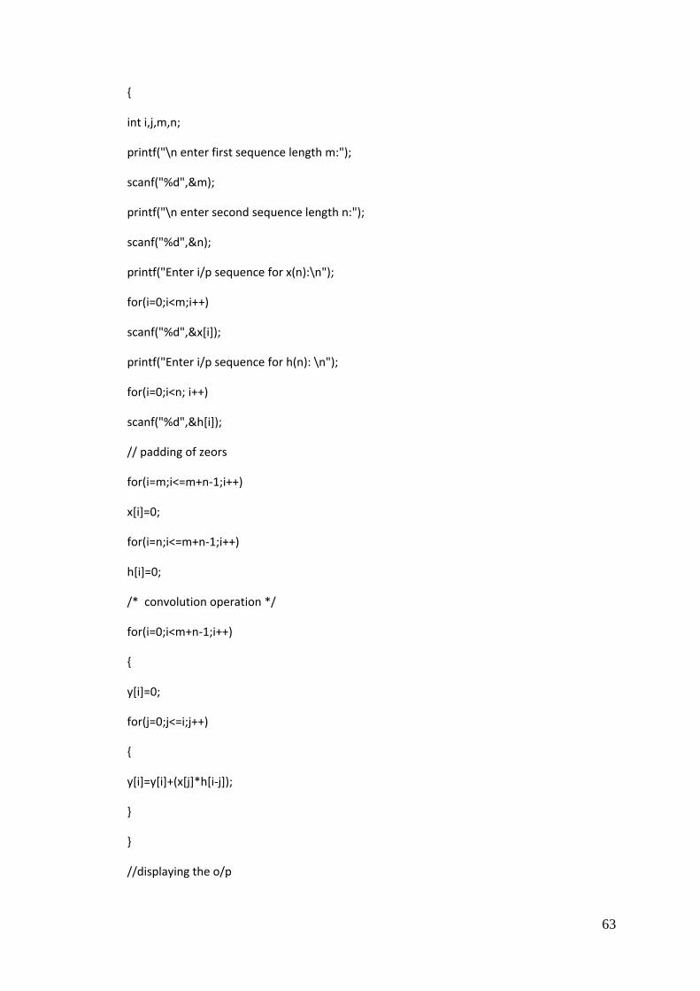
#include<stdio.h>
int x[15],h[15],y[15];
main()
63
{
int i,j,m,n;
printf("\n enter first sequence length m:");
scanf("%d",&m);
printf("\n enter second sequence length n:");
scanf("%d",&n);
printf("Enter i/p sequence for x(n):\n");
for(i=0;i<m;i++)
scanf("%d",&x[i]);
printf("Enter i/p sequence for h(n): \n");
for(i=0;i<n; i++)
scanf("%d",&h[i]);
// padding of zeors
for(i=m;i<=m+n‐1;i++)
x[i]=0;
for(i=n;i<=m+n‐1;i++)
h[i]=0;
/* convolution operation */
for(i=0;i<m+n‐1;i++)
{
y[i]=0;
for(j=0;j<=i;j++)
{
y[i]=y[i]+(x[j]*h[i‐j]);
}
}
//displaying the o/p
64
printf("Output (Linear Convolution) sequence is:\n ");
for(i=0;i<m+n‐1;i++)
printf("y[%d]=%d\t",i,y[i]);
}
PROCEDURE:
Open Code Composer Studio, make sure the DSP kit is turned on.
Start a new project using ‘Project‐new ‘ pull down menu, save it in a
separate directory(c:\ti\myprojects) with name lconv.pjt.
Add the source files conv.asm.
to the project using ‘Project add files to project’ pull down menu.
Add the linker command file hello.cmd.
(Path: c:\ti\tutorial\dsk6713\hello1\hello.cmd)
Add the run time support library file rts6700.lib.
(Path: c:\ti\c6000\cgtools\lib\rts6700.lib)
Compile the program using the ‘Project‐compile’ pull down menu or by
clicking the shortcut icon on the left side of program window.
Build the program using the ‘Project‐Build’ pull down menu or by
clicking the shortcut icon on the left side of program window.
Load the program (lconv.out) in program memory of DSP chip using the
‘File‐load program’ pull down menu.
To View output graphically
Select view graph time and frequency.
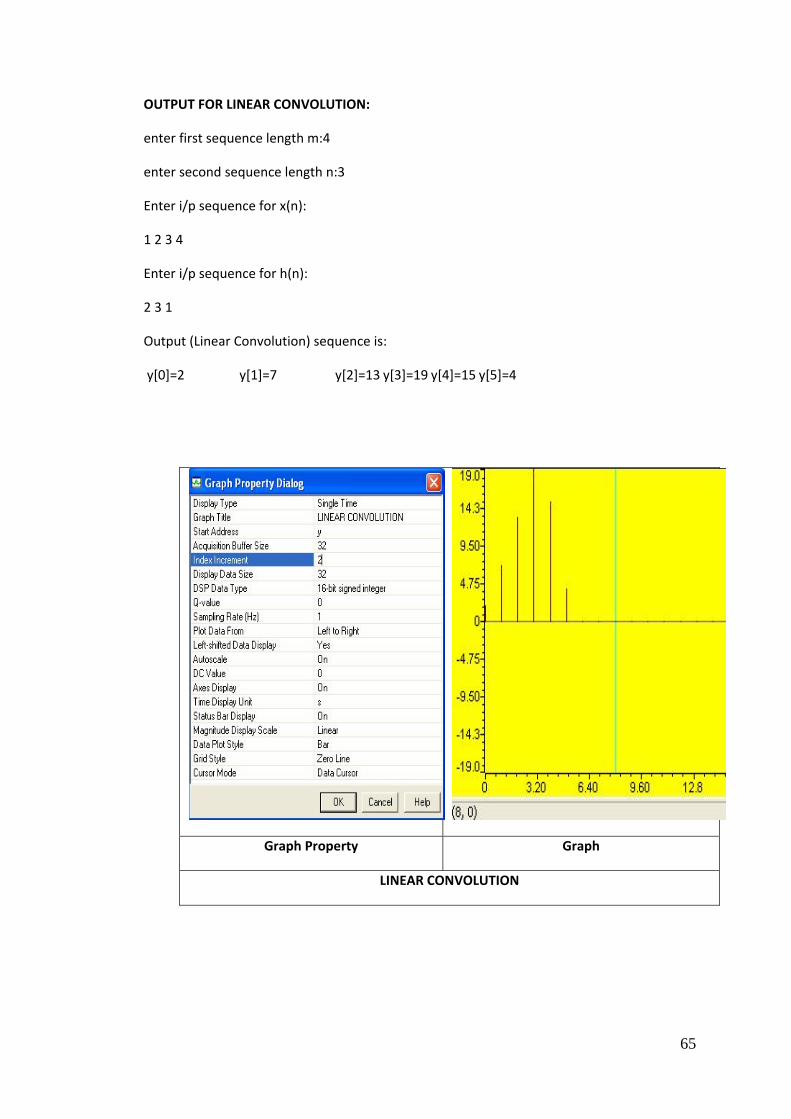
65
OUTPUT FOR LINEAR CONVOLUTION:
enter first sequence length m:4
enter second sequence length n:3
Enter i/p sequence for x(n):
1 2 3 4
Enter i/p sequence for h(n):
2 3 1
Output (Linear Convolution) sequence is:
y[0]=2 y[1]=7 y[2]=13 y[3]=19 y[4]=15 y[5]=4
Graph Property Graph
LINEAR CONVOLUTION
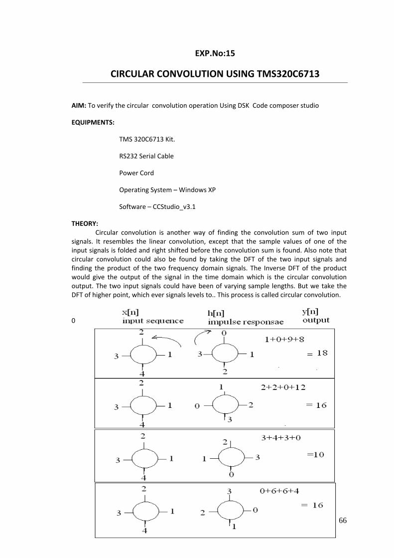
66
EXP.No:15
CIRCULAR CONVOLUTION USING TMS320C6713
AIM: To verify the circular convolution operation Using DSK Code composer studio
EQUIPMENTS:
TMS 320C6713 Kit.
RS232 Serial Cable
Power Cord
Operating System – Windows XP
Software – CCStudio_v3.1
THEORY: Circular convolution is another way of finding the convolution sum of two input
signals. It resembles the linear convolution, except that the sample values of one of the input signals is folded and right shifted before the convolution sum is found. Also note that circular convolution could also be found by taking the DFT of the two input signals and finding the product of the two frequency domain signals. The Inverse DFT of the product would give the output of the signal in the time domain which is the circular convolution output. The two input signals could have been of varying sample lengths. But we take the DFT of higher point, which ever signals levels to.. This process is called circular convolution.
0
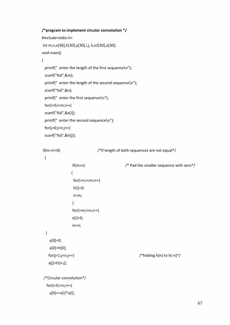
67
/*program to implement circular convolution */
#include<stdio.h>
int m,n,x[30],h[30],y[30],i,j, k,x2[30],a[30];
void main()
{
printf(" enter the length of the first sequence\n");
scanf("%d",&m);
printf(" enter the length of the second sequence\n");
scanf("%d",&n);
printf(" enter the first sequence\n");
for(i=0;i<m;i++)
scanf("%d",&x[i]);
printf(" enter the second sequence\n");
for(j=0;j<n;j++)
scanf("%d",&h[j]);
if(m‐n!=0) /*If length of both sequences are not equal*/
{
if(m>n) /* Pad the smaller sequence with zero*/
{
for(i=n;i<m;i++)
h[i]=0;
n=m;
}
for(i=m;i<n;i++)
x[i]=0;
m=n;
}
y[0]=0;
a[0]=h[0];
for(j=1;j<n;j++) /*folding h(n) to h(‐n)*/
a[j]=h[n‐j];
/*Circular convolution*/
for(i=0;i<n;i++)
y[0]+=x[i]*a[i];

68
for(k=1;k<n;k++)
{
y[k]=0;
/*circular shift*/
for(j=1;j<n;j++)
x2[j]=a[j‐1];
x2[0]=a[n‐1];
for(i=0;i<n;i++)
{
a[i]=x2[i];
y[k]+=x[i]*x2[i];
}
}
/*displaying the result*/
printf(" the circular convolution is\n");
for(i=0;i<n;i++)
printf("%d \t",y[i]);
}
PROCEDURE:
Open Code Composer Studio; make sure the DSP kit is turned on.
Start a new project using ‘Project‐new ‘ pull down menu, save it in a
separate directory(c:\ti\myprojects) with name cir conv.pjt.
Add the source files Circular Convolution.C.
to the project using ‘Project add files to project’ pull down menu.
Add the linker command file hello.cmd .
(Path: c:\ti\tutorial\dsk6713\hello1\hello.cmd)
Add the run time support library file rts6700.lib
(Path: c:\ti\c6000\cgtools\lib\rts6700.lib)
Compile the program using the ‘Project‐compile’ pull down menu or by
clicking the shortcut icon on the left side of program window.
Build the program using the ‘Project‐Build’ pull down menu or by
clicking the shortcut icon on the left side of program window.

69
Load the program(lconv.out) in program memory of DSP chip using the
‘File‐load program’ pull down menu.
OUTPUT FOR CIRCULAR CONVOLUTION:
enter the length of the first sequence
4
enter the length of the second sequence
3
enter the first sequence
1 2 3 4
enter the second sequence
1 2 3
the circular convolution is
18 16 10 16
Graph Property Graph
CIRCULAR CONVOLUTION
70
SRM University
Department of Electronics and Communication Engineering
EC1019A – PROCESSOR LAB
Laboratory Report Cover sheet
ODD Semester – 2015
Name :
Register Number :
Semester / Section :
Batch :
Venue :
Title of the Experiment :
Date of Performance :
Date of Submission :
Particulars Max. Marks Marks Obtained
Pre Lab 05
Post Lab 5
Lab Performance 10
Lab Report 5
Total 25
Report Verification
Staff Name :
Staff Signature :