EBSD in TEM : Introduction to ASTAR system Orientation · PDF fileAlumni–2010 Avignon...
44
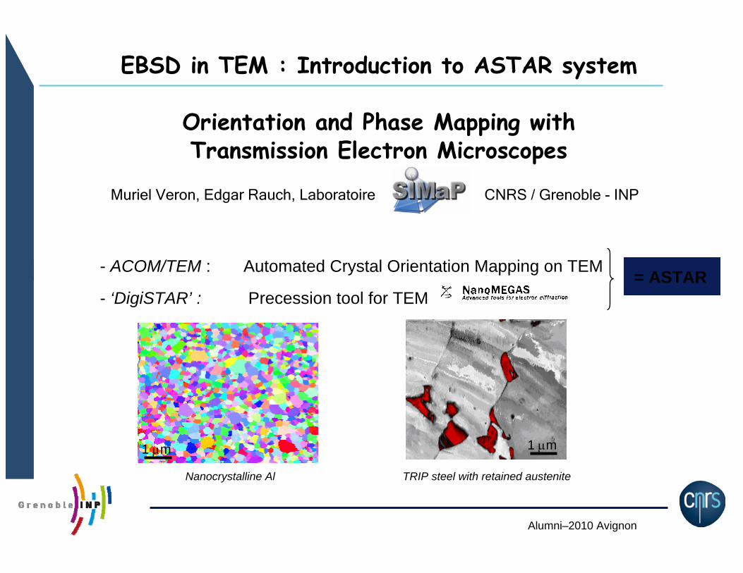
Alumni–2010 Avignon EBSD in TEM : Introduction to ASTAR system Orientation and Phase Mapping with Transmission Electron Microscopes Muriel Veron, Edgar Rauch, Laboratoire CNRS / Grenoble - INP - ACOM/TEM : Automated Crystal Orientation Mapping on TEM - ‘DigiSTAR’ : Precession tool for TEM Nanocrystalline Al TRIP steel with retained austenite 1 m 1 m = ASTAR
Transcript of EBSD in TEM : Introduction to ASTAR system Orientation · PDF fileAlumni–2010 Avignon...
Alumni–2010 Avignon
EBSD in TEM : Introduction to ASTAR system
Orientation and Phase Mapping withTransmission Electron Microscopes
Muriel Veron, Edgar Rauch, Laboratoire CNRS / Grenoble - INP
- ACOM/TEM : Automated Crystal Orientation Mapping on TEM
- ‘DigiSTAR’ : Precession tool for TEM
Nanocrystalline Al TRIP steel with retained austenite
1 m 1 m
= ASTAR
Alumni–2010 Avignon
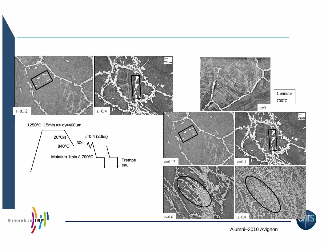
20°C/s
1250°C, 15min => d=400µm
840°C30s
=0.4 (3.6/s)
Trempe eau
Maintien 1min à 700°C
20°C/s
1250°C, 15min => d=400µm
840°C30s
=0.4 (3.6/s)
Trempe eau
Maintien 1min à 700°C
1 minute
700°C

Alumni–2010 Avignon
1
23
4
56
7
89
10
a)
4µm4µm
b) Points
1 2 3 4 5 6 7 8 9 10
c) Code couleur
d) e)

Alumni–2010 Avignon
Deformed austenite (Fe-Ni alloy), EBSD quality contrast, and TEM observations
ZONE-1
ZONE-2
ZONE-3
ZONE-1
ZONE-2
ZONE-3
Joint de grains
0
2
4
6
8
10
0 200 400 600 800 1000 1200 1400 1600
Déplacement (nm)
Déso
rient
atio
n (°)
désorientation point par pointdésorientation cumulée
EBSD index quality contrast
BF TEM observations

Alumni–2010 Avignon
3) ASTAR
Combining orientation/phase identification with Electron Precession
1) Example of application in metallurgy
Recrystallization of ferritic stainless steelsCollaboration with N. Meyer, Ugitech
2) ACOM/TEM
Template matching
Template generation and pattern acquisition

Alumni–2010 Avignon
Microstructural optimization for magnetic actuators
• Alloys compositionsAISI EN C N Cr Nb
430 1.4016 0.017 0.028 16.083 0.004
430Nb 1.4511 0.015 0.012 16.284 0.27
% Cr
Cr2N Nb(C,N)
% Cr
Area without Chromium2 µm
- Ferritic Stainless steel 430 (A1 = 880°C)
- Stabilized Ferritic stainless steel: 430Nb (feriitic at all T)

Alumni–2010 Avignon
Deformed state Static recovery Static recrystallizationG
rain
sca
leSu
bgra
ins
1 µm1 µm 2 µm2 µm2 µm
Recovery Recrystallized fraction

Alumni–2010 Avignon
1 µm
Bright Field
1 µm
Bright Field Orientation mapOrientation mappoint number
Mis
orie
ntat
ion
(°)
point to origin misorientationpoint to point misorientation
point numberM
isor
ient
atio
n (°
)
point to origin misorientationpoint to point misorientation
Nucleation mecanisms : SIBM, typical for law strain level
430 : 7 min @ 850°C
430 : 1 h @ 850°C
• Recrystallization mechanism– Nucleation
• We did not observed large misorientation, even in recovered area
Complementary observation of bulging at GB’s
Alumni–2010 Avignon
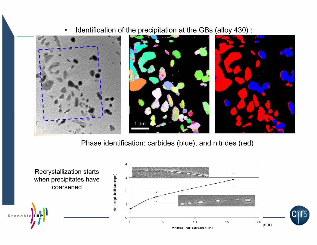
• Identification of the precipitation at the GBs (alloy 430) :
Phase identification: carbides (blue), and nitrides (red)
Recrystallization starts when precipitates have
coarsened

Alumni–2010 Avignon
2) ACOM/TEM : Automated Crystal Orientation Mapping
Severely
deformed
7075 Al. Alloy
1 µm
WC-Co
0.5 m
Orientation map (Al alloy) Phase map WC-Co

Alumni–2010 Avignon
ACOM/TEM : Automated Crystal Orientation Mapping
Severely
deformed
7075 Al. Alloy
1 µm Orientation Orientation + ’(= +0.1°)
Kikuchi pattern
Bragg Spot pattern

Alumni–2010 Avignon
ACOM/TEM : Orientation Indexing
Diffraction pattern for arandomly oriented crystal
Calculated diffraction pattern
orientation
Austenite, ferrite, one or two grains?
Alumni–2010 Avignon
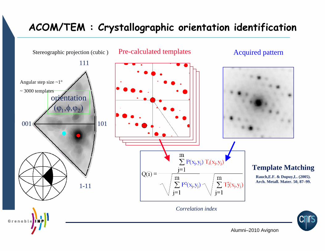
ACOM/TEM : Crystallographic orientation identification
Acquired pattern
Correlation index
111
001 101
1-11
Pre-calculated templatesStereographic projection (cubic )
orientation
Angular step size ~1°
~ 3000 templates
Template MatchingRauch,E.F. & Dupuy,L. (2005). Arch. Metall. Mater. 50, 87–99.
Alumni–2010 Avignon
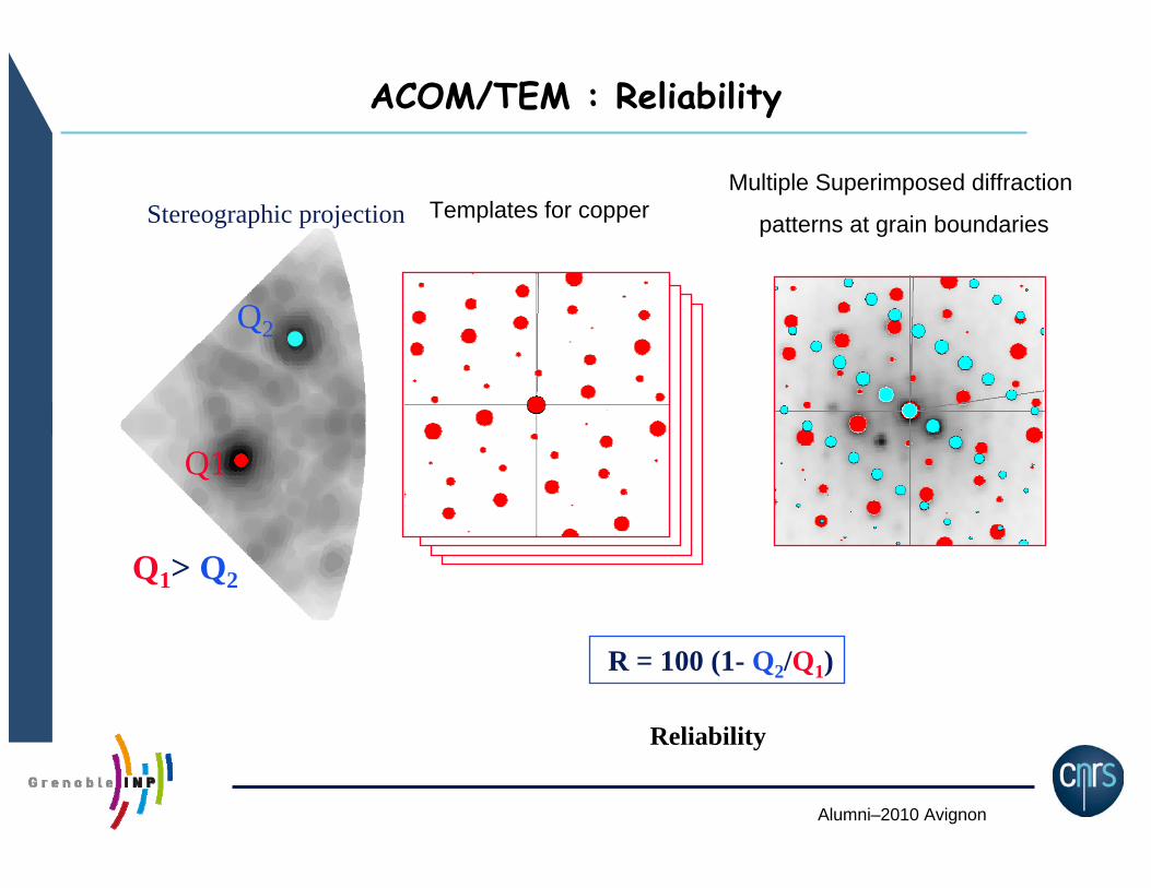
Reliability
Stereographic projection
R = 100 (1- Q2/Q1)
Q2
Q1
Q1> Q2
ACOM/TEM : Reliability
Multiple Superimposed diffraction
patterns at grain boundariesTemplates for copper

Alumni–2010 Avignon
ACOM/TEM : Phase identification and reliability
Ferrite : Index I1 = 553 Austenite : Index I2 = 389
Phase reliability (= 30)
PR = 100 (1- I2/I1)Austenite, ferrite ?

Alumni–2010 Avignon
TEMdpa : Diffraction Pattern Acquisition
Features:• up to 180 fps
• easy selection of the area of interest
• single or movie type DP acquisition
• brightness, contrast, exposure time control
• On line Virtual Bright Field construction
Computer
Beam Control
Image processing
D/A board
Frame GrabberCamera
Beam control through dedicated SSTAR unit
Diffraction pattern acquisition
Computer
Beam Control
Image processing
D/A board
Frame GrabberCamera
Computer
Beam Control
Image processing
D/A board
Frame GrabberCamera
Beam control through dedicated SSTAR unit
Diffraction pattern acquisition
ASTAR unit

Alumni–2010 Avignon
‘Bright field’ : Heavily deformed Cu(=8) (ECAP)
1 µm
400x300 steps
14 nm
Reliability
Virtual bright field
Bright field

Alumni–2010 Avignon
Deformed Cu (coll. N. Llorca – Univ. Barcelona, Spain) Orientation reliability
Correlation Index Phase Reliability Orientations
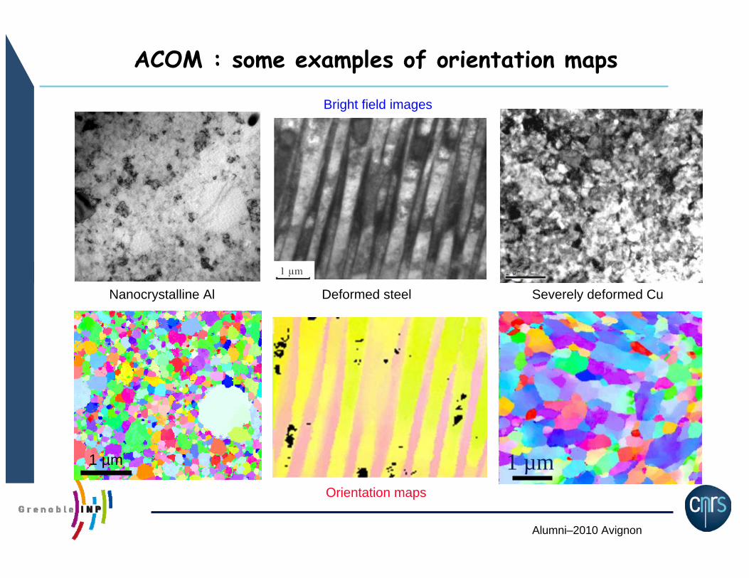
ACOM : some examples of orientation maps
Fe 1.67% C (HT 10 min @ 1100°C, A. Stormvinter - KTH) Austenite Martensite
Alumni–2010 Avignon
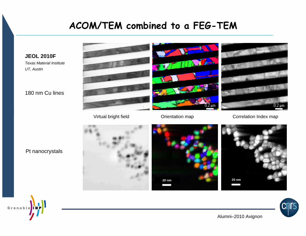
Virtual bright field Orientation map Correlation Index map
20 nm 20 nm
180 nm Cu lines
Pt nanocrystals
ACOM/TEM combined to a FEG-TEM
JEOL 2010FTexas Material InstituteUT, Austin
Alumni–2010 Avignon
2) ASTAR :
Combining orientation/phase identification with Electron Precession
1) ACOM/TEM :
Template matching
Pattern acquisition and template generation
Alumni–2010 Avignon
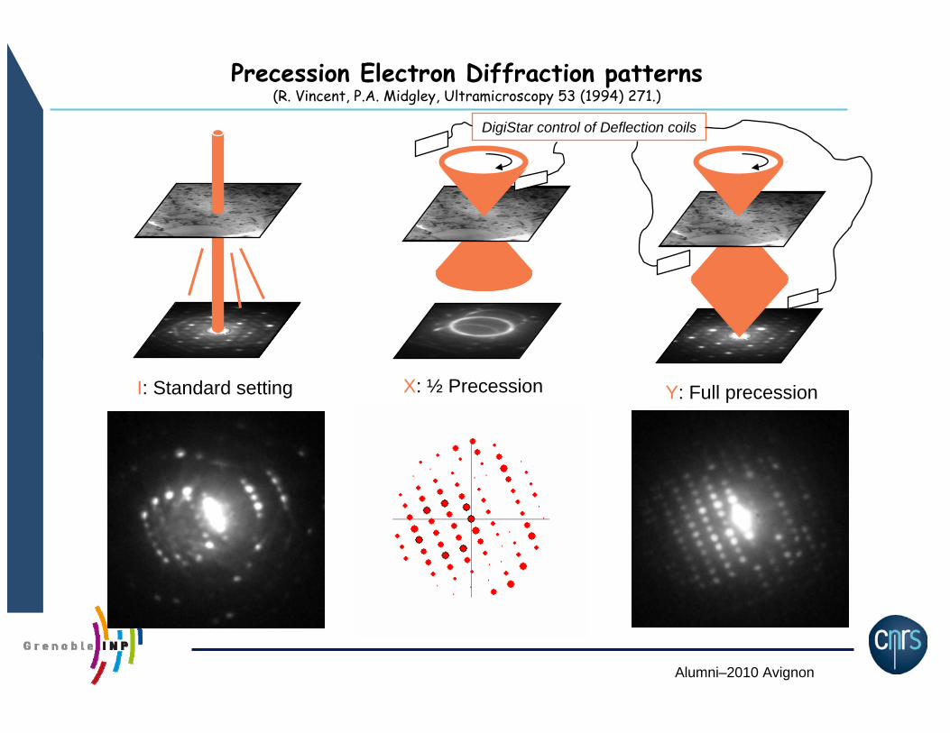
Precession Electron Diffraction patterns (R. Vincent, P.A. Midgley, Ultramicroscopy 53 (1994) 271.)
I: Standard setting X: ½ Precession Y: Full precession
DigiStar control of Deflection coils

Alumni–2010 Avignon
Precession Electron Diffraction patterns
Mayenite crystal (Ca12Al14O33) : space group I-43d
Without precession
With precession precession angle : 0.35º acquisition time 50 min (10 fps)
Orientation Index Virtual Bright Field

Alumni–2010 Avignon
0.5µm
Deformation of Aluminum film
Alumni–2010 Avignon
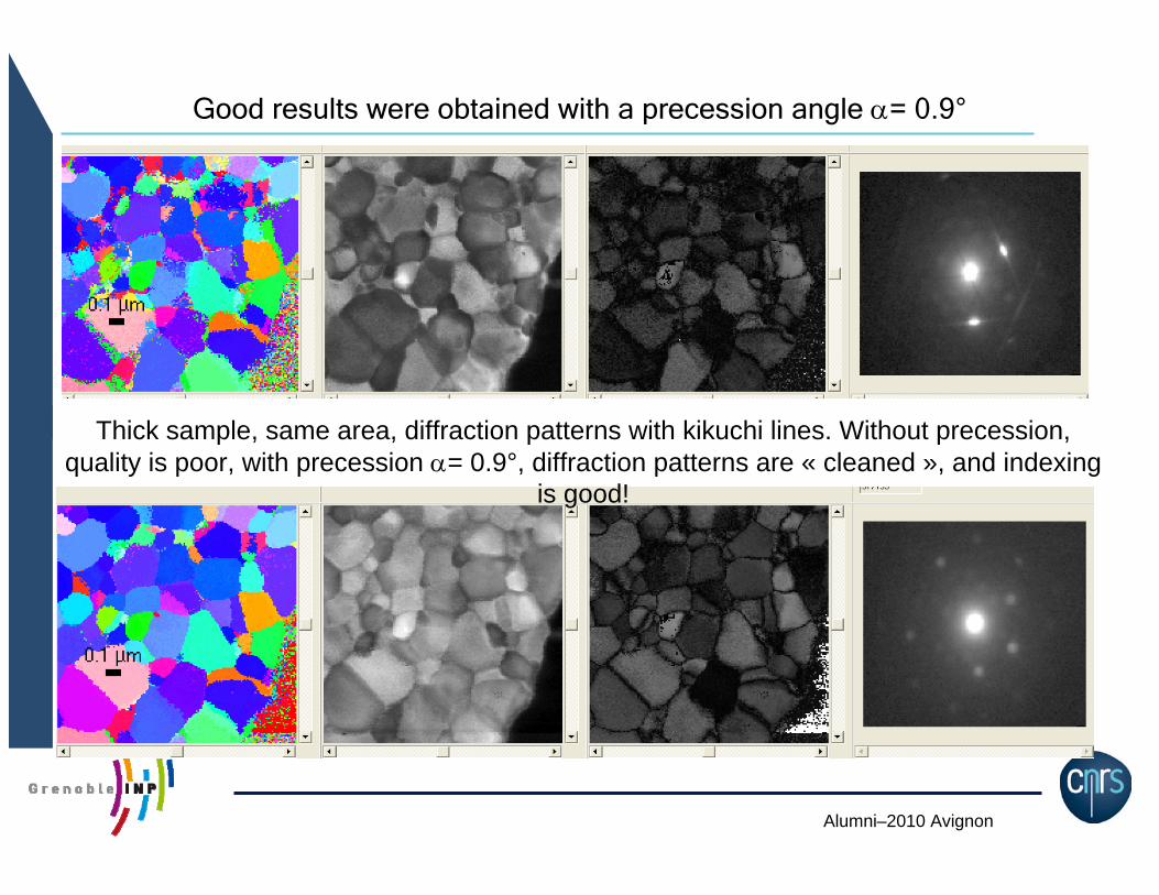
Good results were obtained with a precession angle = 0.9°
Thick sample, same area, diffraction patterns with kikuchi lines. Without precession, quality is poor, with precession = 0.9°, diffraction patterns are « cleaned », and indexing
is good!
Alumni–2010 Avignon

Alumni–2010 Avignon

Alumni–2010 Avignon
Diffraction patterns collected on a
Philips CM120 (LaB6, 120 kV)
ACOM + Precession: Solving 180° orientation ambiguities
B.c.c. Iron (ferrite), [112]Without precession
I : Index=317, Reliability=0
Y : Index=670, Reliability=28
Rotation angle (around the normal axis)
Inde
xIn
dex
With precession (1.5°)

Alumni–2010 Avignon
ACOM + Precession: Solving 180° orientation ambiguities
Precession angle 0.5°Fe-1.5%Cu (annealed)
[115]
[315]Orientation ambiguities
Alumni–2010 Avignon
DiffGen : Template generator
Alumni–2010 Avignon
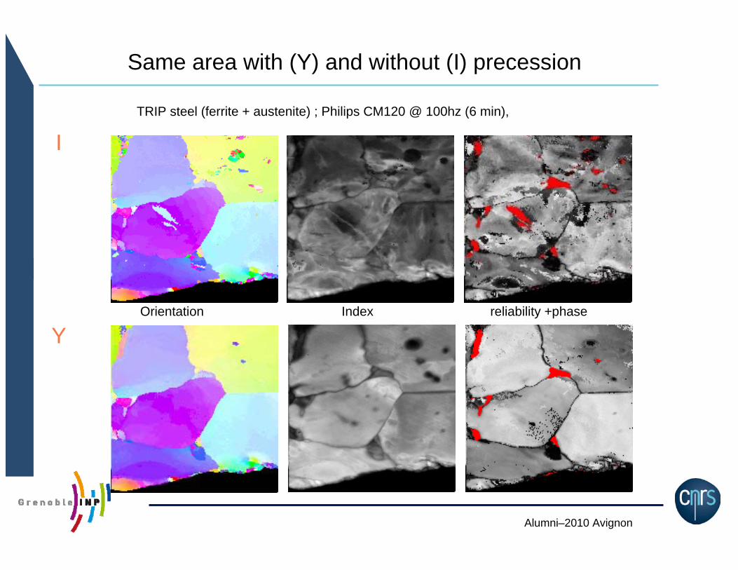
Same area with (Y) and without (I) precession
I
YOrientation Index reliability +phase
TRIP steel (ferrite + austenite) ; Philips CM120 @ 100hz (6 min),
Alumni–2010 Avignon
INDEX : pattern identification software

Alumni–2010 Avignon
Alumni–2010 Avignon
ACOM : some examples of orientation maps
1 µm 1 µm
Nanocrystalline Al Deformed steel Severely deformed Cu
Bright field images
Orientation maps

Alumni–2010 Avignon
Grain size and Texture in 80 nm copper lines
Side view
SIDE VIEW (orientation and index superimposed map)The two scans were performed with different settingsThey demonstrated the reproducibility of the identification
300 nm500x100 steps (6.5 nm each) , Spot size 25 nm Scanning time : 19 min (44 fps)
250x100 steps (13 nm each) LaB6 equipped Jeol 3010 TEM (spot size 25 nm)Scanning time : 10 min (44 fps)
CROSS VIEW (orientation map)
Grain size of the order of 30 nm may be identify despite the use of a conventional LaB6 equipped Jeol 3010 TEM (spot size 25 nm).A fiber texture was detected within the channel.
300x100 steps (6.5 nm each), spot size 15 nm Scanning time : 12 min (44 fps)
Credits: - Stefan BRANDSTETTER, SIMaP - Grenoble INP
500 nm

Alumni–2010 Avignon
6 nm
Indexing Fourier transform of High resolution TEM images
TITAN-Cubed : PbSe nanocrystals
Credits: - Marie CHEYNET, SIMaP - Grenoble INP- Odile ROBBE, LASIR – UTS Lille
128 pixels = 3 nm
256 pixels = 6 nm
FFT over 128x128subimages
FFT over 256x256subimages
Fast Fourier Transforms are performed on successive subsets of the high resolution image as if the sample was scanned.
The resulting patterns are compared to templates
Orientations and/or phases may be recognized
-a small subset leads to higher spatial resolution- larger subimages improve the indexing quality
Orientation map (color) combined to INDEX (gray scale)

Alumni–2010 Avignon
ACOM/TEM : Automated Crystal Orientation MappingFe 1.67% C (HT 10 min @ 1100°C, A. Stormvinter - KTH)
Austenite
Martensite
Orientation map
Phase map

Alumni–2010 Avignon
ACOM : orientation and phase maps
TRIP steel with retained austenite
Orientation maps Virtual bright field Correlation Index Phase + reliability

Alumni–2010 Avignon
Deformed Cu (coll. N. Llorca – Univ. Barcelona, Spain)
Bright field Correlation Index Reliability Orientations
Severely Deformed Fe (coll. S. Descartes – LaMCoS, Lyon - France)
ACOM : some examples of orientation maps
Alumni–2010 Avignon
Alumni–2010 Avignon
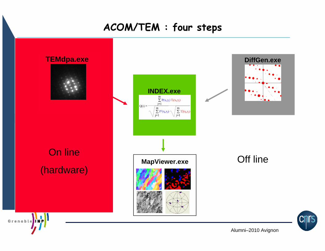
On line
(hardware)Off line
ACOM/TEM : four steps
TEMdpa.exe DiffGen.exe
INDEX.exe
MapViewer.exe

Alumni–2010 Avignon
DiffGen : Template generator
Features: Any crystallographic structure, any orientation
Laue class related to the space group
Structure generator (lattice, cell, structure factor)
Alumni–2010 Avignon
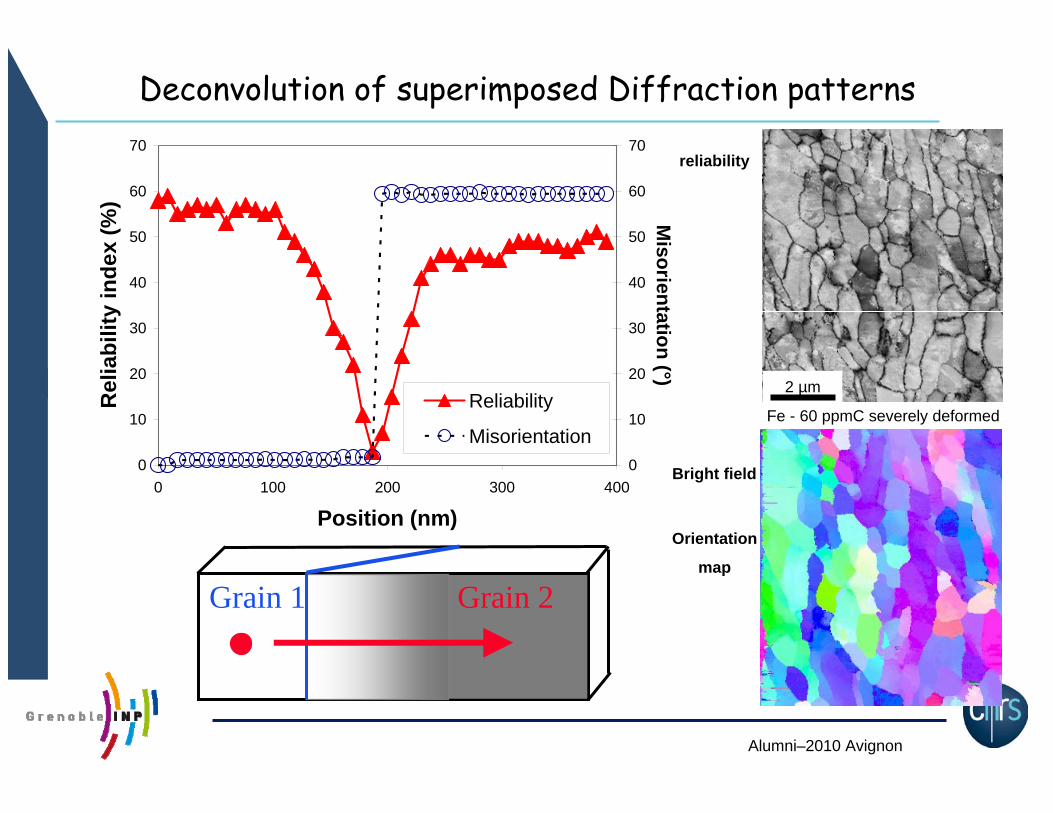
Fe - 60 ppmC severely deformed
Deconvolution of superimposed Diffraction patterns
Grain 1 Grain 2
0
10
20
30
40
50
60
70
0 100 200 300 400
Position (nm)
Rel
iabi
lity
inde
x (%
)
Reliability
Misorientation0
10
20
30
40
50
60
70
0 100 200 300 400
Position (nm)
Rel
iabi
lity
inde
x (%
)
0
10
20
30
40
50
60
70
Misorientation (°)
Reliability
Misorientation
2 µm2 µm
reliability
Bright field
Orientation
map

Alumni–2010 Avignon
Orientation map ‘ Bright field ‘
TEMdpa : Virtual Bright Field on-line construction
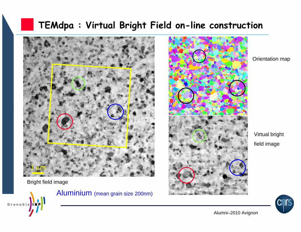
Alumni–2010 Avignon
Orientation map
Bright field image
Virtual bright
field image
TEMdpa : Virtual Bright Field on-line construction
Aluminium (mean grain size 200nm)
1 m