E cient Implementations of WiMAX OFDM Functions on Recon ...
143
Efficient Implementations of WiMAX OFDM Functions on Reconfigurable Platforms by Ahmad Sghaier A thesis presented to the University of Guelph in fulfilment of the thesis requirement for the degree of MSc.(Eng) in Engineering Systems and Computing Guelph, Ontario, Canada, 2009 c Ahmad Sghaier 2009
Transcript of E cient Implementations of WiMAX OFDM Functions on Recon ...

Efficient Implementations of WiMAX OFDM
Functions on Reconfigurable Platforms
by
Ahmad Sghaier
A thesis
presented to the University of Guelph
in fulfilment of the
thesis requirement for the degree of
MSc.(Eng)
in
Engineering Systems and Computing
Guelph, Ontario, Canada, 2009
c©Ahmad Sghaier 2009
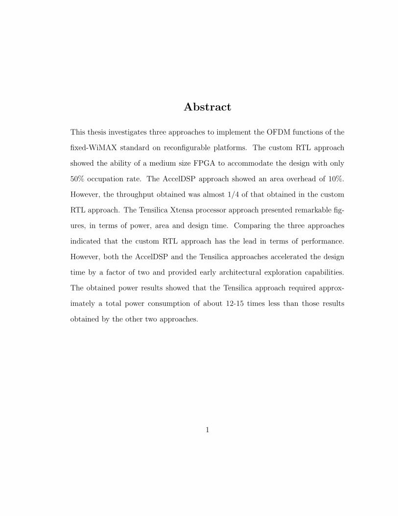
Abstract
This thesis investigates three approaches to implement the OFDM functions of the
fixed-WiMAX standard on reconfigurable platforms. The custom RTL approach
showed the ability of a medium size FPGA to accommodate the design with only
50% occupation rate. The AccelDSP approach showed an area overhead of 10%.
However, the throughput obtained was almost 1/4 of that obtained in the custom
RTL approach. The Tensilica Xtensa processor approach presented remarkable fig-
ures, in terms of power, area and design time. Comparing the three approaches
indicated that the custom RTL approach has the lead in terms of performance.
However, both the AccelDSP and the Tensilica approaches accelerated the design
time by a factor of two and provided early architectural exploration capabilities.
The obtained power results showed that the Tensilica approach required approx-
imately a total power consumption of about 12-15 times less than those results
obtained by the other two approaches.
1

I hereby declare that I am the sole author of this thesis.
I authorize the University of Guelph to lend this thesis to other institutions or
individuals for the purpose of scholarly research.
I further authorize the University of Guelph to reproduce this thesis by photo-
copying or by other means, in total or in part, at the request of other institutions
or individuals for the purpose of scholarly research.
i

The University of Guelph requires the signatures of all persons using or photo-
copying this thesis. Please sign below, and give address and date.
ii

Acknowledgments
I would like to take this opportunity to express my sincere appreciation to my
supervisor professor Shawki Areibi for his guidance and assistance, and for the
help he provided throughout this Master program. Many thanks to professor Radu
Muresan and professor Robert Dony for reviewing this thesis. I would like to thank
the Libyan Higher Education Department for the scholarship they provided me.
I want to especially thank my wife Halima, my mother and my brothers and
sisters for their continuous encouragement and support.
And finally, many thanks to all my friends. Special thanks to Mahdi Elghazali
and Ahmed Elhossini, I really enjoyed the time we spent together. Thanks to all
the people who helped me by any means. I also would like to thank two of the
most valuable friends I have ever had Mohamed Sharif and Ahmed Elwan, you
were always of great support.
iii

To
my wife and the little Kenda
for the sacrifice they made and for the joy they brought me.
iv
Contents
1 Introduction 1
1.1 Motivation and Objectives . . . . . . . . . . . . . . . . . . . . . . . 2
1.1.1 Motivation . . . . . . . . . . . . . . . . . . . . . . . . . . . . 2
1.1.2 Objectives . . . . . . . . . . . . . . . . . . . . . . . . . . . . 3
1.2 Overview of Research Work . . . . . . . . . . . . . . . . . . . . . . 3
1.3 Contributions . . . . . . . . . . . . . . . . . . . . . . . . . . . . . . 5
1.4 Thesis Organization . . . . . . . . . . . . . . . . . . . . . . . . . . . 6
2 Background 7
2.1 Wireless Communication Technology . . . . . . . . . . . . . . . . . 8
2.1.1 Wireless Communication Concepts . . . . . . . . . . . . . . 9
2.2 Broadband Wireless Access . . . . . . . . . . . . . . . . . . . . . . 10
2.3 What is WiMAX? . . . . . . . . . . . . . . . . . . . . . . . . . . . . 11
2.3.1 The IEEE 802.16 Suite . . . . . . . . . . . . . . . . . . . . . 11
2.3.2 Competitive Technologies . . . . . . . . . . . . . . . . . . . 13
2.4 WiMAX PHY Layer and OFDM . . . . . . . . . . . . . . . . . . . 14
2.4.1 WiMAX PHY Layer . . . . . . . . . . . . . . . . . . . . . . 14
v
2.4.2 OFDM . . . . . . . . . . . . . . . . . . . . . . . . . . . . . . 15
2.4.3 Implementing OFDM . . . . . . . . . . . . . . . . . . . . . . 17
2.5 Reconfigurable Computing Systems . . . . . . . . . . . . . . . . . . 20
2.5.1 Field Programmable Gate Arrays . . . . . . . . . . . . . . . 20
2.5.2 FPGA Internals . . . . . . . . . . . . . . . . . . . . . . . . . 22
2.6 Application Specific Instruction-set Processors . . . . . . . . . . . . 23
2.6.1 The Tensilica ASIPs . . . . . . . . . . . . . . . . . . . . . . 25
2.7 Summary . . . . . . . . . . . . . . . . . . . . . . . . . . . . . . . . 26
3 Literature Review 27
3.1 The Two Poles . . . . . . . . . . . . . . . . . . . . . . . . . . . . . 27
3.1.1 Pure Software Implementation . . . . . . . . . . . . . . . . . 28
3.1.2 ASIC Implementation . . . . . . . . . . . . . . . . . . . . . 32
3.2 Filling the Gap . . . . . . . . . . . . . . . . . . . . . . . . . . . . . 35
3.2.1 FPGAs . . . . . . . . . . . . . . . . . . . . . . . . . . . . . 36
3.2.2 ASIPs . . . . . . . . . . . . . . . . . . . . . . . . . . . . . . 43
3.3 Summary . . . . . . . . . . . . . . . . . . . . . . . . . . . . . . . . 47
4 Methodology 48
4.1 Protocol Stack and Scope of Work . . . . . . . . . . . . . . . . . . . 49
4.2 Methodology . . . . . . . . . . . . . . . . . . . . . . . . . . . . . . 50
4.2.1 Analysis and Abstraction . . . . . . . . . . . . . . . . . . . . 51
4.2.2 Design and Coding . . . . . . . . . . . . . . . . . . . . . . . 54
4.2.3 Testing and Integration . . . . . . . . . . . . . . . . . . . . . 54
4.3 Design Environment . . . . . . . . . . . . . . . . . . . . . . . . . . 55
vi

4.4 Summary . . . . . . . . . . . . . . . . . . . . . . . . . . . . . . . . 56
5 Custom RTL Implementation 57
5.1 Transmitter Design Details . . . . . . . . . . . . . . . . . . . . . . . 58
5.1.1 Randomization . . . . . . . . . . . . . . . . . . . . . . . . . 58
5.1.2 Forward Error Correction . . . . . . . . . . . . . . . . . . . 59
5.1.3 Interleaver . . . . . . . . . . . . . . . . . . . . . . . . . . . . 63
5.1.4 Constellation Mapper . . . . . . . . . . . . . . . . . . . . . . 66
5.1.5 Pilot and Zero Insertion . . . . . . . . . . . . . . . . . . . . 67
5.1.6 IFFT . . . . . . . . . . . . . . . . . . . . . . . . . . . . . . . 69
5.1.7 Cyclic Prefix Insertion . . . . . . . . . . . . . . . . . . . . . 69
5.2 Receiver Design Details . . . . . . . . . . . . . . . . . . . . . . . . . 71
5.3 Results . . . . . . . . . . . . . . . . . . . . . . . . . . . . . . . . . . 74
5.3.1 Resource Utilization . . . . . . . . . . . . . . . . . . . . . . 75
5.3.2 Timing Results . . . . . . . . . . . . . . . . . . . . . . . . . 76
5.3.3 Comparison . . . . . . . . . . . . . . . . . . . . . . . . . . . 77
5.4 Summary . . . . . . . . . . . . . . . . . . . . . . . . . . . . . . . . 79
6 AccelDSP Implementation 81
6.1 AccelDSP Design Flow . . . . . . . . . . . . . . . . . . . . . . . . . 82
6.1.1 AccelDSP Basics and Features . . . . . . . . . . . . . . . . . 82
6.1.2 Synthesis Flow . . . . . . . . . . . . . . . . . . . . . . . . . 85
6.2 Transmitter Design and Trade-offs . . . . . . . . . . . . . . . . . . . 87
6.2.1 Design Trade-offs . . . . . . . . . . . . . . . . . . . . . . . . 88
6.3 Results . . . . . . . . . . . . . . . . . . . . . . . . . . . . . . . . . . 91
vii
6.3.1 AccelDSP vs. Custom RTL . . . . . . . . . . . . . . . . . . 92
6.4 Summary . . . . . . . . . . . . . . . . . . . . . . . . . . . . . . . . 94
7 Configurable Processors Implementation 96
7.1 Tensilica Configurable Processors . . . . . . . . . . . . . . . . . . . 97
7.1.1 Xtensa Processors . . . . . . . . . . . . . . . . . . . . . . . . 97
7.1.2 Design Flow . . . . . . . . . . . . . . . . . . . . . . . . . . . 99
7.2 Design Details . . . . . . . . . . . . . . . . . . . . . . . . . . . . . . 99
7.2.1 Design Environment and Overall Architecture . . . . . . . . 101
7.2.2 Profiling Results . . . . . . . . . . . . . . . . . . . . . . . . 102
7.3 Results . . . . . . . . . . . . . . . . . . . . . . . . . . . . . . . . . . 105
7.3.1 Performance and Area . . . . . . . . . . . . . . . . . . . . . 105
7.3.2 Power . . . . . . . . . . . . . . . . . . . . . . . . . . . . . . 106
7.4 Overall Comparison . . . . . . . . . . . . . . . . . . . . . . . . . . . 106
7.5 Summary . . . . . . . . . . . . . . . . . . . . . . . . . . . . . . . . 109
8 Conclusion 110
8.1 Future Work . . . . . . . . . . . . . . . . . . . . . . . . . . . . . . . 112
Bibliography 114
A Glossary 120
B AccelDSP Flow 122
C IEEE 802.16-2004 Standard 125
C.1 Example of an OFDM uplink . . . . . . . . . . . . . . . . . . . . . 125
viii

C.2 Constellations . . . . . . . . . . . . . . . . . . . . . . . . . . . . . . 127
ix

List of Tables
2.1 IEEE 802.16 Standards . . . . . . . . . . . . . . . . . . . . . . . . . 13
2.2 WiMAX OFDM Parameters . . . . . . . . . . . . . . . . . . . . . . 19
3.1 Industrial WiMAX ASIC Implementation . . . . . . . . . . . . . . . 35
4.1 OFDM symbol parameters . . . . . . . . . . . . . . . . . . . . . . . 52
4.2 Coding, Interleaving and Modulation rates . . . . . . . . . . . . . . 53
5.1 The puncturing configuration for the convolutional encoder . . . . . 63
5.2 Transmitter and Receiver IPs Resource Utilization . . . . . . . . . . 76
5.3 Transceiver Resource Utilization . . . . . . . . . . . . . . . . . . . . 77
5.4 Timing Results . . . . . . . . . . . . . . . . . . . . . . . . . . . . . 78
5.5 This work vs. Garcia’s implementation . . . . . . . . . . . . . . . . 78
5.6 This work vs. Lattice Semiconductor implementation . . . . . . . . 79
6.1 RS Encoder Memory mapping Trade-off . . . . . . . . . . . . . . . 89
6.2 Pilot Insert Memory mapping Trade-off . . . . . . . . . . . . . . . . 90
6.3 CP Insert Memory mapping Trade-off . . . . . . . . . . . . . . . . . 90
6.4 Interleaver Rolling-unrolling Trade-off . . . . . . . . . . . . . . . . . 91
x
6.5 AccelDSP Transmitter Resource Utilization . . . . . . . . . . . . . 91
6.6 AccelDSP Transmitter IPs Resource Utilization . . . . . . . . . . . 92
6.7 AccelDSP vs. Pure VHDL Transmitter Implementation . . . . . . . 94
7.1 Xtensa Processor Configuration Detail . . . . . . . . . . . . . . . . 101
7.2 Profiling Results (Pure C Code vs TIE-extended Code) . . . . . . . 103
7.3 Profiling Results (with compiler directives enabled) . . . . . . . . . 104
7.4 Power/Energy Results (Pure C Code vs TIE-extended Code) . . . . 106
7.5 The Three Approaches Trading Table . . . . . . . . . . . . . . . . . 108
xi
List of Figures
1.1 Research Approach . . . . . . . . . . . . . . . . . . . . . . . . . . . 4
2.1 Wireless Standards Coverage . . . . . . . . . . . . . . . . . . . . . . 9
2.2 Orthogonality in OFDM . . . . . . . . . . . . . . . . . . . . . . . . 16
2.3 Simplex point-to-point transmission using OFDM. . . . . . . . . . . 18
2.4 Generic FPGA Architecture [12] . . . . . . . . . . . . . . . . . . . . 22
2.5 FPGA Internals [11] . . . . . . . . . . . . . . . . . . . . . . . . . . 24
3.1 Parallelism in the Scrambling Unit . . . . . . . . . . . . . . . . . . 28
3.2 Concatenated FEC Block . . . . . . . . . . . . . . . . . . . . . . . 29
3.3 Shared vs. dedicated FFT operation . . . . . . . . . . . . . . . . . 42
4.1 Scope of Work . . . . . . . . . . . . . . . . . . . . . . . . . . . . . . 50
4.2 The methodology applied in this work . . . . . . . . . . . . . . . . 51
4.3 IEEE 802.16-2004 Transmitter . . . . . . . . . . . . . . . . . . . . . 53
5.1 PRBS Generator for Randomization . . . . . . . . . . . . . . . . . . 59
5.2 RS Encoder Stages . . . . . . . . . . . . . . . . . . . . . . . . . . . 61
5.3 Convolutional Encoder of rate 1/2 . . . . . . . . . . . . . . . . . . . 62
xii

5.4 Interleaver internal architecture . . . . . . . . . . . . . . . . . . . . 65
5.5 Permutation table contents (case of 192 bits interleaver size) . . . . 65
5.6 Mapper internal architecture . . . . . . . . . . . . . . . . . . . . . . 67
5.7 PRBS generator for pilot generation . . . . . . . . . . . . . . . . . . 68
5.8 IFFT to other blocks connection . . . . . . . . . . . . . . . . . . . . 70
5.9 Cyclic Prefix Insertion Stage . . . . . . . . . . . . . . . . . . . . . . 71
5.10 Receiver Block Diagram . . . . . . . . . . . . . . . . . . . . . . . . 72
5.11 Demapper internal architecture . . . . . . . . . . . . . . . . . . . . 73
6.1 AccelDSP ISE Synthesis Flow (Courtesy of Xilinx Inc. [40]). The
numbers indicate the sequence required by the flow . . . . . . . . . 86
7.1 Xtensa Design Flow . . . . . . . . . . . . . . . . . . . . . . . . . . . 100
B.1 The AccelDSP System Generator Synthesis Flow . . . . . . . . . . 123
B.2 The AccelDSP HW Co-sim Synthesis Flow . . . . . . . . . . . . . . 124
C.1 The Different Constellations for the Used Modulation Schemes . . . 128
xiii
Chapter 1
Introduction
The rapid growth of the Internet and cellular services recently has dictated
an increasing demand for communication standards that provide high data rate,
mobility and convergence. Broadband wireless access (BWA) is increasingly gaining
popularity as an option for the last-mile connection replacing cable modems and
DSL connections [1]. In specific, WiMAX, the IEEE 802.16 standard, came as
a follow-up to the successful 802.11 wireless local area network (LAN) standard,
with deployments of the IEEE 802.16 wireless metropolitan area network (MAN)
standard currently in progress. The standard aims to provide both fixed broadband
wireless access for rural and remote areas, as well as to support mobility for users
of hand held and small devices.
In parallel, Reconfigurable Computing (RC) platforms have been attracting the
attention of developers in the last decade due to the increasing computational capa-
bility they posses. These platforms in addition to their computational capabilities
are also characterized by their flexibility, reprogammability and fast and easy de-
1

CHAPTER 1. INTRODUCTION 2
sign cycle. Therefore, designers and manufacturers are starting to consider them as
a main option in their platforms arsenal. In addition, design tools for these plat-
forms provide means to trade-off the implementation results as well as the design
time and flexibility. Thus, the investigation of the different available tools is worth
considering, which is one of the main topics of this dissertation.
1.1 Motivation and Objectives
1.1.1 Motivation
Broadband wireless access is the newly adopted trend in enabling broadband access
for fixed and mobile users, with deployments expected to increase by 3 times by 2010
[1]. Furthermore, general purpose processors and application specific integrated
circuits do not either have the performance nor the flexibility for implementing so-
phisticated and still-in-development algorithms. On the other hand, the capability
of reconfigurable platforms (FPGAs in specific) have been increasing and shift-
ing these platforms from being prototyping-only platforms to a mass-production
option. Todays RCs’ capabilities and the fact that current wireless communica-
tion standards are still in the development phase promote RCs as a viable option
in implementing these developing standards to provide features such as in-field
programmability. Thus investigating different approaches for implementing these
standards will provide some insight to direct the designers in their design method-
ology.

CHAPTER 1. INTRODUCTION 3
1.1.2 Objectives
The objective of this thesis is to investigate the suitability of three implementation
approaches on RCs in terms of area, performance, power and design time. The
objective is to guide the designer toward the best approach in his/her selection
criteria based on a specific factor. The detailed objectives of this thesis can be
summarized as following:
• To evaluate the three approaches and identify the best performer according
to the criterion.
• To perform early design exploration through utilizing the AccelDSP tool.
• To provide a library of Intellectual Proprieties (IPs) that can be utilized by
researchers to implement the targeted standard and other similar standards.
• To verify the designed IPs through implementing the OFDM chain of the
WiMAX transmitter and receiver.
1.2 Overview of Research Work
The research approach in implementing the OFDM functions of the IEEE 802.16-
2004 standard on reconfigurable platforms is depicted in Figure 1.1.
Implementing the standard on a RC platform started by analyzing the blocks to
be implemented, defining their architecture and specifying the interfacing between
them. From this analysis, several points of interest were identified including the
reliance of most of these blocks on memory elements (RAMs and ROMs), and that
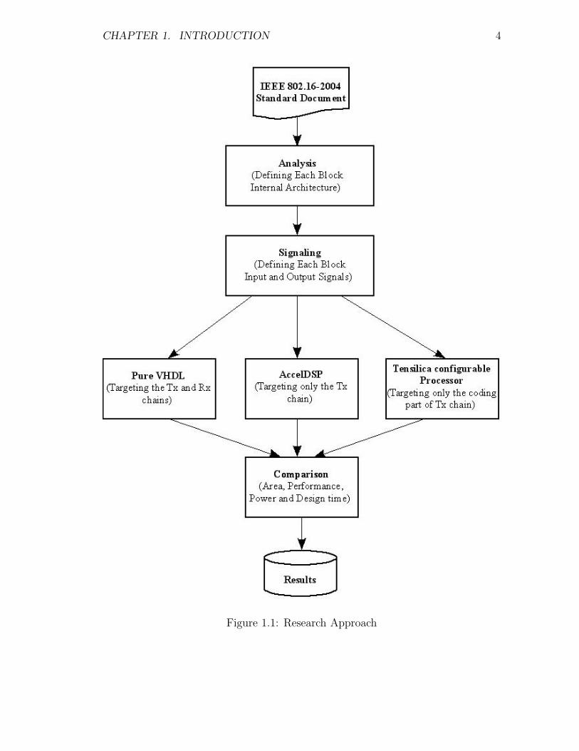
CHAPTER 1. INTRODUCTION 4
Figure 1.1: Research Approach

CHAPTER 1. INTRODUCTION 5
other blocks tend to rely on bits manipulation. At the beginning two approaches
targeting FPGAs were explored, and later the configurable processors approach was
added to the list of investigation. In the first approach, a custom RTL (VHDL)
implementation targeting the transmitting and receiving chains was pursued. In
the second approach, a high level approach represented by the AccelDSP tool was
used to compare it with the previous approach. Results obtained indicated the
suitability of this approach for fast designs, early design trade-offs and architecture
exploration. The third approach, ASIPs, looked at a narrower scope, by only
implementing the coding part of the transmitting chain to provide further trade-off
analysis for interested designers. The approach targets the Tensilica configurable
processors which promise fast design time and remarkable performance figure. The
results obtained by the three approaches were compared and presented to show the
suitability of each approach for a specific criteria (area, performance, power or fast
development cycle).
1.3 Contributions
The work presented here provides any interested designer/researcher with the main
trade-offs between the different available designing approaches to map wireless com-
munication standards, and other signal processing algorithms, on reconfigurable
platforms. The main contributions of this thesis can be summarized as:
• Investigating three different implementation approaches to map the OFDM
functions of the IEEE 802.16-2004 standard on reconfigurable platforms.

CHAPTER 1. INTRODUCTION 6
• Providing the interested reader with the trade-off results to show the suit-
ability of each approach according to certain parameters such as: area, per-
formance, power and design time.
• Building two IPs libraries: synthesizable VHDL IPs for both the transmitting
and receiving chains and system generator blocks for the transmitting chain.
• Submitting the obtained results for publication in the CCECE08 [2] and
FPL08 [3] conferences.
1.4 Thesis Organization
The thesis is organized as following: Chapter 2 introduces the main concepts of wire-
less communication and WiMAX and the targeted platforms (FPGAs and ASIPs).
Chapter 3 provides an overview on the previously conducted work in implementing
OFDM-based systems on GPPs, ASICs, FPGAs and ASIPs. Chapter 4 explains
the main methodology followed in the implementation, as well as specifying the
scope of work and describing the working environment.
Chapter 5 explains in details the custom RTL approach, and lists the obtained
results while comparing them to similar previously conducted work. Chapter 6 ad-
dresses the AccelDSP approach, and it concludes by comparing the obtained results
with the custom RTL approach. Chapter 7 tends to investigate the configurable
processors approach limiting the implementation to specific functions, and compar-
ing the results obtained to the previous two approaches. The thesis concludes in
Chapter 8 with suggestions for future work.

Chapter 2
Background
In broadband wireless communication, designs need to meet a number of critical
requirements, such as processing speed, flexibility, and fast time to market. These
requirements direct the designers in their criteria to select the targeted hardware
platform. Therefore, to support high data rates, the underlying hardware platform
must have significant processing capabilities. In addition, several advanced signal
processing techniques, such as coding/decoding and modulation, are very compu-
tationally intensive and require a significant number of multiply and accumulate
(MAC) operations per second.
Moreover, most of the newly adopted wireless communication standards, such
as WiMAX, are currently going through the initial development and deployment
stages. Thus, having hardware flexibility/reprogrammability is very important,
which will ensure in-field programmability as the standard evolves. Finally, time to
market is a key differentiator for success in gaining a market share, which directly
affects the choice of hardware platform, where designers usually seek easy-to-use
7
CHAPTER 2. BACKGROUND 8
development tools and available Intellectual Property (IP) libraries. Reconfigurable
computing platforms promote themselves as a remarkable solution for developing
broadband wireless systems such as WiMAX, with their computational capabilities,
flexibility and fast design cycle.
In this chapter, the necessary background information related to broadband
wireless access, orthogonal frequency division multiplexing (OFDM) and WiMAX
technologies will be presented.
2.1 Wireless Communication Technology
Wireless communication is the field that relies on sharing the air to exchange in-
formation. The field noticed a significant growth since the introduction of Wire-
less Local Area Network standards. The geographic scale of the available wireless
standards ranges from Wireless Personal Area Networks (WPAN) which is a net-
work for interconnecting devices centered around an individual person’s workspace -
about 10 meters distance. Among the WPAN standards are ZigBee (IEEE802.15.4)
and Bluetooth (IEEE802.15.1) standards. The latter is used primarily to connect
personal gadgets, while ZigBee was designed for remote monitoring and control
applications with low power requirement.
The wider range is WLAN, which is represented by the WiFi (Wireless Fidelity),
IEEE 802.11a/b/g/n, standards. WLAN is able to accommodate data rates up
to 54 Mbps in 802.11a/g standards and up to 600Mbps in the newly introduced
IEEE802.11n standard, and with a coverage of 35-100 meters. The widest wire-
less coverage is presented in the Wireless Metropolitan and Wide Area Networks
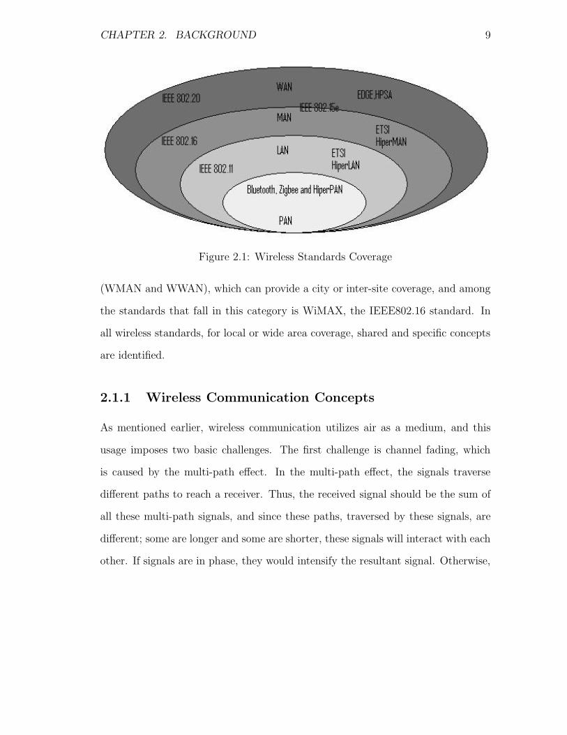
CHAPTER 2. BACKGROUND 9
Figure 2.1: Wireless Standards Coverage
(WMAN and WWAN), which can provide a city or inter-site coverage, and among
the standards that fall in this category is WiMAX, the IEEE802.16 standard. In
all wireless standards, for local or wide area coverage, shared and specific concepts
are identified.
2.1.1 Wireless Communication Concepts
As mentioned earlier, wireless communication utilizes air as a medium, and this
usage imposes two basic challenges. The first challenge is channel fading, which
is caused by the multi-path effect. In the multi-path effect, the signals traverse
different paths to reach a receiver. Thus, the received signal should be the sum of
all these multi-path signals, and since these paths, traversed by these signals, are
different; some are longer and some are shorter, these signals will interact with each
other. If signals are in phase, they would intensify the resultant signal. Otherwise,

CHAPTER 2. BACKGROUND 10
the resultant signal is weakened since the received signals are out of phase, which
leads to two different types of signal transmission over the wireless channel. Thus,
the radio channel of a wireless communication system is often described as being
either Line-of-sight (LOS) or Non-line-of-sight (NLOS). In a LOS link, the signal
travels over a direct and unobstructed path from the transmitter to the receiver,
while in NLOS the signal reaches the receiver through reflections, scattering, and
diffractions. The signals arriving at the receiver consists of components from the
direct path, multiple reflected paths, scattered energy, and diffracted propagation
paths.
The second challenge attributed to using air as the medium is interference,
which is caused by the other transmitting sources, in-path objects or external
noises. Other types of interference that is caused by the way the systems oper-
ate include Inter-Symbol Interference (ISI) and Inter-Carrier Interference (ICI). in
ISI, the previous symbol acts as a source of noise, which will affect the following
symbol. On the other hand, ICI occurs between the different subcarriers used to
form a single symbol.
2.2 Broadband Wireless Access
Broadband Wireless Access (BWA) has emerged as one of the most attractive
solutions for the last mile access technology for residential and small and medium
sized businesses. The growth of BWA has been inspired by the growth in the
broadband sector, where Internet services has spread to reach a billion users around
the globe. On the other hand, wireless mobile service subscribers have also reached

CHAPTER 2. BACKGROUND 11
more than 2 billion in 2005 [1].
In the last two decades, technologies such as cable and Digital Subscriber Line
(DSL) are providing the service for most of the Internet users, and cellular tech-
nologies are providing the service for mobile users. However, the cable and DSL
technologies are facing issues with installation in areas that lack cable and telephone
structures such as in developing countries and also in remote areas in developed
countries. In the cellular service, the technologies are still unable to provide high
data rate to enable broadband access, and here comes the contribution of BWA.
Firstly, it is faster, cheaper and easier to deploy than DSL and cable, and this BWA
flavor provides fixed broadband wireless access. Secondly, the other flavor is of high
data rate and supports mobility to enable nomadic and mobile services.
The BWA solution that encompasses both BWA flavors is known as WiMAX
(Worldwide Interoperability for Microwave Access), which has been released in dif-
ferent versions (a,b,c,d,e) under the name IEEE802.16 standard. Later, the stan-
dard was adopted by the WiMAX forum for interoperability considerations.
2.3 What is WiMAX?
2.3.1 The IEEE 802.16 Suite
Even though wireless communication systems have been in use for some time, none
of them were able to provide broadband wireless services with high data rate, wide
coverage and support for mobility. The initiative by the IEEE organization, started
in 1998, has produced a set of standards that address the previously mentioned

CHAPTER 2. BACKGROUND 12
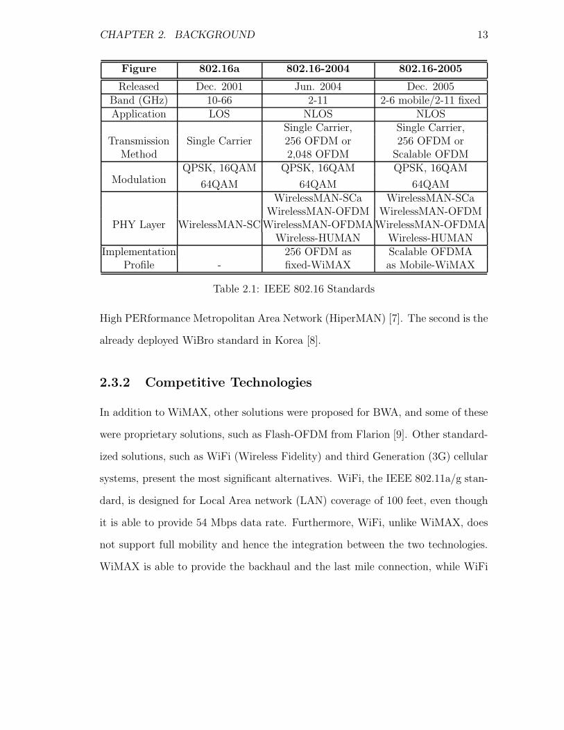
concerns. The proposed WiMAX standard, IEEE 802.16, has evolved over a period
of six years to be finalized in two distinctive standards.
The first standard was released in its final version in June 2004 [4], IEEE 802.16-
2004, and was named Fixed-WiMAX. Fixed-WiMAX addresses fixed broadband
wireless services, and initially it targeted the Line-of-sight (LOS) deployment for
point-to-multipoint systems. The standard was based on a single-carrier physical
(PHY) layer operation in the 11-66 GHz frequency band. Latter amendments
utilized OFDM-based PHY layer to enable Non Line-of-sight (NLOS) deployments
in the 2-11 GHz band. In December 2005, the Mobile-WiMAX standard [5], IEEE
802.16e-2005, was released to support nomadicity and mobility. Both standards,
fixed and mobile, have accommodated different design options for PHY layer, MAC
(Medium Access Control) layer, duplexing and frequency band to suit a variety of
applications and deployment scenarios. The different standards and their specific
parameters are listed in Table 2.1, compiled from [1].
In order to make WiMAX products interoperable, the WiMAX forum [6] has
been established to look after reducing the standard options into a number of
system and certification profiles. So far, the WiMAX forum has defined two sys-
tems profiles. The first is the fixed system profile based on the IEEE 802.16-2004
OFDM PHY layer, and the other is the mobile system profile based on the IEEE
802.16e-2005 scalable OFDMA. The forum has also specified a number of certifica-
tion profiles; five for the fixed profile and fourteen for the mobile profile.
Finally, there are other released standards that are similar to WiMAX. The first
is the contribution by the European Telecommunication Standards Institute (ETSI)
CHAPTER 2. BACKGROUND 13
Figure 802.16a 802.16-2004 802.16-2005
Released Dec. 2001 Jun. 2004 Dec. 2005Band (GHz) 10-66 2-11 2-6 mobile/2-11 fixedApplication LOS NLOS NLOS
Single Carrier, Single Carrier,Transmission Single Carrier 256 OFDM or 256 OFDM or
Method 2,048 OFDM Scalable OFDMQPSK, 16QAM QPSK, 16QAM QPSK, 16QAM
Modulation 64QAM 64QAM 64QAMWirelessMAN-SCa WirelessMAN-SCa
WirelessMAN-OFDM WirelessMAN-OFDMPHY Layer WirelessMAN-SC WirelessMAN-OFDMA WirelessMAN-OFDMA
Wireless-HUMAN Wireless-HUMANImplementation 256 OFDM as Scalable OFDMA
Profile - fixed-WiMAX as Mobile-WiMAX
Table 2.1: IEEE 802.16 Standards
High PERformance Metropolitan Area Network (HiperMAN) [7]. The second is the
already deployed WiBro standard in Korea [8].
2.3.2 Competitive Technologies
In addition to WiMAX, other solutions were proposed for BWA, and some of these
were proprietary solutions, such as Flash-OFDM from Flarion [9]. Other standard-
ized solutions, such as WiFi (Wireless Fidelity) and third Generation (3G) cellular
systems, present the most significant alternatives. WiFi, the IEEE 802.11a/g stan-
dard, is designed for Local Area network (LAN) coverage of 100 feet, even though
it is able to provide 54 Mbps data rate. Furthermore, WiFi, unlike WiMAX, does
not support full mobility and hence the integration between the two technologies.
WiMAX is able to provide the backhaul and the last mile connection, while WiFi

CHAPTER 2. BACKGROUND 14
should cover the hotspot, office and home areas.
The other competitor is the 3G technologies used by mobile operators - GSM
(Global System for Mobile Communication) or CDMA (Code Division Multiple
Access), such as HSPA (High Speed Packet Access) and 1x EV-DO (1x Evolution
Data Optimized). All these technologies provide a data rate in the range of 100’s
of Kbps up to few Mbps, while WiMAX could reach up to 64 Mbps in downlink
and 7 Mbps in uplink. Moreover, WiMAX differentiate itself from the cellular
technologies by supporting symmetric backhaul links - T1/E1 links. However, if
the high speed mobility factor was considered, the 3G technologies will outperform
WiMAX. This is due to the early consideration of this factor in the design of 3G
technologies, while it was an add-on to the initial WiMAX standard.
Accordingly, WiMAX fills the gap between the available technologies, WiFi and
3G, when we consider factors such as data rate, coverage, mobility and price.
2.4 WiMAX PHY Layer and OFDM
2.4.1 WiMAX PHY Layer
In the released documents, IEEE 802.16-2004 and IEEE 802.16e-2005, a number of
PHY layers were introduced to support different scenarios and applications. The
first released standard in 2001 revealed a PHY layer design that is based on a
single carrier system and targeting LOS deployments in the frequency band 10-66
GHz. Later, an OFDM-based PHY layer was introduced to address applications
that work in the NLOS environments, and in the frequency band of 2-11 GHz.
CHAPTER 2. BACKGROUND 15
The OFDM-based PHY layer was the most adopted one by the manufacturers due
to its advantages over single carrier systems, and especially in multipath fading
channels. Also, the reputation gained from adopting OFDM in DSL, WiFi and
other communication standards, paved the way for the OFDM-based PHY layer in
WiMAX.
2.4.2 OFDM
Prior to introducing OFDM, multiplexing techniques will be discussed briefly. Like
all computing systems, multiplexing was the natural way to accommodate several
users (channels) on a single link. The need for multiplexing techniques arises from
the need for: the capability to compress data in order to encode certain characters
with fewer bits than normally required; the capability to detect and correct errors
between the two points being connected to ensure data integrity, and the capability
to manage transmission resources on a dynamic basis.
Among the widely known multiplexing techniques are FDM (Frequency Division
Multiplexing) and TDM (Time Division Multiplexing). FDM divides the entire fre-
quency band available on the communications link into smaller individual bands or
channels, and each user is assigned to a different frequency. On the other hand,
TDM assigns a dedicated time slot for each user on the system, and in a predeter-
mined sequence each user is allocated a time slot during which it can transmit.
The problems associated with the previously mentioned multiplexing techniques
are the difficulty to reconfigure in an environment with high degree of dynamic
change for FDM systems, and the wasted bandwidth when vacant slots occur be-
CHAPTER 2. BACKGROUND 16
cause of idle users in TDM systems. Moreover, FDM works by adding a guard band
between the subcarriers which also wastes the available bandwidth.
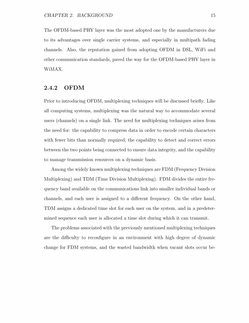
The multiplexing technique introduced here (OFDM) is also, similar to FDM,
based on the Multi-Carrier Modulation (MCM) transmission technique. The prin-
ciple of MCM describes the division of the input bit stream into several parallel
bit streams that are then used to modulate several sub carriers. Each subcarrier is
separated by a guard band to ensure that they do not overlap with each other. In
the receiver side, bandpass filters are used to separate the spectrum of individual
subcarriers.
Figure 2.2: Orthogonality in OFDM
CHAPTER 2. BACKGROUND 17
OFDM is a special form of spectrally efficient MCM technique, which employs
densely spaced orthogonal subcarriers and overlapping spectrum, as seen in Figure
2.2. The use of bandpass filters are not required in OFDM because of the orthog-
onality nature of the subcarriers. In Figure 2.2, the effect of this is seen as the
required bandwidth is greatly reduced by removing the guard bands and allowing
the subcarriers to overlap. It is still possible to recover the individual subcarriers
despite their overlapping spectrum provided that the orthogonality is maintained.
Because of the combination of multiple low data rate subcarriers, OFDM pro-
vides a composite high data rate with long symbol duration. This in effect, de-
pending on the channel coherence time, reduces or completely eliminates the risk
of InterSymbol Interference (ISI), which is a common phenomenon in a multipath
channel environment. The use of Cyclic Prefix (CP) in OFDM symbol can further
reduce the effect of ISI [10], and this is governed by the length of the CP.
2.4.3 Implementing OFDM
The principles of OFDM were published in the late 50’s and early 60’s as an efficient
MCM technique. However, due to technical implementation constraints, e.g. digital
FFT/IFFT implementation, OFDM deployment was delayed at that time. By 1965,
Cooley and Tukey, [10], presented the algorithm for FFT calculation and later its
efficient implementation in hardware, which brought OFDM back to life and enabled
chip makers to put OFDM into work.
The digital implementation of OFDM system is achieved through the math-
ematical operations called discrete Fourier transform (DFT) and its counterpart
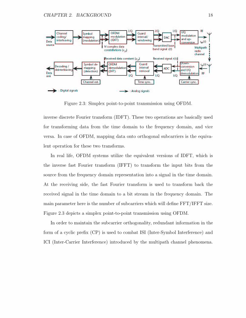
CHAPTER 2. BACKGROUND 18
Figure 2.3: Simplex point-to-point transmission using OFDM.
inverse discrete Fourier transform (IDFT). These two operations are basically used
for transforming data from the time domain to the frequency domain, and vice
versa. In case of OFDM, mapping data onto orthogonal subcarriers is the equiva-
lent operation for these two transforms.
In real life, OFDM systems utilize the equivalent versions of IDFT, which is
the inverse fast Fourier transform (IFFT) to transform the input bits from the
source from the frequency domain representation into a signal in the time domain.
At the receiving side, the fast Fourier transform is used to transform back the
received signal in the time domain to a bit stream in the frequency domain. The
main parameter here is the number of subcarriers which will define FFT/IFFT size.
Figure 2.3 depicts a simplex point-to-point transmission using OFDM.
In order to maintain the subcarrier orthogonality, redundant information in the
form of a cyclic prefix (CP) is used to combat ISI (Inter-Symbol Interference) and
ICI (Inter-Carrier Interference) introduced by the multipath channel phenomena.
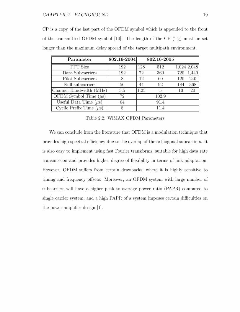
CHAPTER 2. BACKGROUND 19
CP is a copy of the last part of the OFDM symbol which is appended to the front
of the transmitted OFDM symbol [10]. The length of the CP (Tg) must be set
longer than the maximum delay spread of the target multipath environment.
Parameter 802.16-2004 802.16-2005
FFT Size 192 128 512 1,024 2,048Data Subcarriers 192 72 360 720 1,440Pilot Subcarriers 8 12 60 120 240Null subcarriers 56 44 92 184 368
Channel Bandwidth (MHz) 3.5 1.25 5 10 20OFDM Symbol Time (µs) 72 102.9
Useful Data Time (µs) 64 91.4Cyclic Prefix Time (µs) 8 11.4
Table 2.2: WiMAX OFDM Parameters
We can conclude from the literature that OFDM is a modulation technique that
provides high spectral efficiency due to the overlap of the orthogonal subcarriers. It
is also easy to implement using fast Fourier transforms, suitable for high data rate
transmission and provides higher degree of flexibility in terms of link adaptation.
However, OFDM suffers from certain drawbacks, where it is highly sensitive to
timing and frequency offsets. Moreover, an OFDM system with large number of
subcarriers will have a higher peak to average power ratio (PAPR) compared to
single carrier system, and a high PAPR of a system imposes certain difficulties on
the power amplifier design [1].

CHAPTER 2. BACKGROUND 20
2.5 Reconfigurable Computing Systems
Reconfigurable Computing Systems (RCS) is a paradigm that utilizes programmable
logic to accelerate the computation of complex algorithms. The interest in RCS
started in 1980’s [11] with the spread of Complex Programmable Logic Devices
(CLPDs), and later Field Programmable Gate Arrays (FPGAs). The field of RCS
provides an acceleration in the range of 10X to 100X to the equivalent software al-
gorithm, which motivated communication systems developers recently to consider
it as a primary technology [12].
The speed advantage of RCS is based on the fact that the used hardware is
customized to perform a certain algorithm and also has customized bit-width to
avoid excessive power and area usage. Therefore, the RCS system will contain
less functional units, up to the point, and will outperform also systems that are
based on general purpose or digital signal processors. On the other hand, RCS
provides a degree of flexibility to accommodate developing algorithms and support
design update. In contrast, Application Specific Integrated Circuits (ASICs) have
the design engraved in silicon, not flexible, but they still have a higher performance
and a lower power consumption than FPGAs.
2.5.1 Field Programmable Gate Arrays
Field Programmable Gate Arrays (FPGAs) are digital Integrated Circuits (ICs)
that could be seen as a two dimensional array of programmable logic blocks, which
are connected through programmable interconnects. Each logic block, in the sim-
plest form, is a Look-Up Table (LUT), which can be used to implement Boolean
CHAPTER 2. BACKGROUND 21
functions. The internal logic blocks are connected to the outside world through
a number of I/O blocks. These FPGAs are categorized as fine-grained FPGAs.
However, larger and more complex algorithms required the introduction of coarse-
grained FPGAs, that include specific blocks such as: embedded block RAM, mul-
tipliers and Multiply-and-Accumulate (MAC) blocks. Moreover, to speedup the
design time designers tend to resort to the already designed Intellectual Property
(IP) cores.
FPGAs are considered as a solution that resides in the middle ground between
software processor-based solutions and application oriented ICs. The main advan-
tages of FPGAs are [12]:
• Quick time to market.
• No non-recurring engineering costs for fabrication.
• Reprogrammable, permitting both upgrading and device reuse.
• Easy to fix for design errors.
• Support for changing algorithms and standards.
• Reusability, in terms of IPs and developed code.
• Less expensive for low volumes or in prototyping.
Of course, when FPGAs are compared with ASICs, FPGAs cost more for high
production volumes. Also, in terms of speed, ASIC designs still outperform FPGA-
based designs. However, the new trend today that uses state-of-the-art CMOS

CHAPTER 2. BACKGROUND 22
processes indicates that FPGAs are approaching the performance ASICs provide
in many systems [12].
2.5.2 FPGA Internals
Generally, FPGAs internals are divided into three components: logic blocks, routing
elements, and input/output blocks. FPGAs are seen as an array of programmable
logic blocks that can be interconnected to each other, and to the I/O blocks, through
the programmable routing elements. Figure 2.4 depicts a generic FPGA architec-
ture.
Figure 2.4: Generic FPGA Architecture [12]
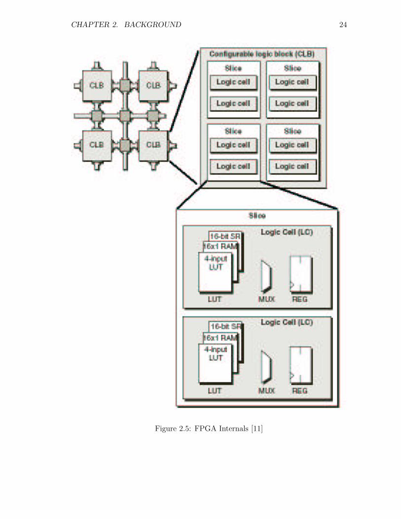
FPGA logic blocks are grouped in a hierarchical order. Each of the logic blocks,
sometimes referred to as Logic Cells (LCs), is based on using an LUT, a multiplexer
and a flip-flop, as shown in Figure 2.5. In a more complex LCs, 4/5/6-input LUTs,
number of multiplexers and flip-flops and fast carry chain logic could be found
inside an LC. The next step in the hierarchy is grouping a number of LCs, usually

CHAPTER 2. BACKGROUND 23
two, inside a slice. The slices are then merged in groups of two or four to form the
Configurable Logic Blocks (CLBs). The reason behind this hierarchy of elements is
to keep the faster interconnects inside the clustered elements, and having relatively
slower interconnects as we step up in the hierarchy [11].
Other parts of FPGAs, in coarser architectures, include embedded block or
distributed RAM on the periphery of the chip or in arranged columns. These
blocks could be utilized to implement single and dual-port RAMs as well as First-
In-First-Out (FIFO) functions. In addition, multipliers, adders and MACs are also
forming a part of the FPGA architecture, and they usually reside next to the block
RAMs. Finally, embedded processors can be easily mapped on the FPGA fabric in
the form of hard or soft cores [11].
2.6 Application Specific Instruction-set Proces-
sors
High speed, flexibility and low power dissipation, for computationally demanding
algorithms are becoming a necessity in today’s complex designs. Traditional archi-
tecture solutions are usually in the form of an ASIC or DSP processors. While ASIC
are characterized by their computation efficiency, they are not flexible enough to
support updates of the implemented algorithms. On the other hand, even though
DSP processors are flexible and programmable, they lag in terms of performance
and power consumption. Thus, the recent new flexible architectures of Application
Specific Instruction-set Processors (ASIPs) can replace multiple chip designs imple-
CHAPTER 2. BACKGROUND 24
Figure 2.5: FPGA Internals [11]
CHAPTER 2. BACKGROUND 25
mented as an ASIC architecture, and still being flexible and however at the same
time being able to be application specific, unlike the DSP. ASIPs can be defined
as the heterogeneous platforms composed of programmable processor core and cus-
tomized hardware modules that allow the designers to extend the instruction set
with application-specific instructions.
Two approaches normally used for ASIP synthesis. The first attempts to cus-
tomize an available processor and the second builds the data paths from scratch.
The major drawback with manually customized ASIPs made them unattractive to
designers since it takes months to develop the specific C compilers. However, re-
cently, high-level development CAD tools brought ASIPs closer to the category of
easy-fast-design approaches.
2.6.1 The Tensilica ASIPs
A novel popular approach of ASIP synthesis is the Tensilica Xtensa configurable
processors [13], which is based on two principles: configurability and extensibility.
The ASIP processors from Tensilica, allow the designer to configure the processor
and specify the required functional units. In addition, when the designer is unsat-
isfied with the performance, he/she can still extend the processor Instruction Set
Architecture (ISA). The specific instruction set enables the application speed-up,
while fixing errors and modifying the processor can be achieved in several hours.
The supporting design tools allow fast and efficient processor design whose duration
is comparable to the purely programmable DSP solutions.
Tensilica processors are represented by either the off-the-shelf cores via the Di-

CHAPTER 2. BACKGROUND 26
amond Standard Series or by the full configurable cores via the Xtensa processor
family. The Diamond series covers a range of performance scenarios with five cores,
which include a small 32-bit controller as well as a high performance audio/video
engines. The other family, the Xtensa processors, are fully-featured configurable
processors that can be defined at the micro-architectural level with the possibility
of significant adaptation to the base processor to reflect specific application re-
quirements. Further details about the Tensilica processors and the design flow is
discussed in Chapter 7.
2.7 Summary
BWA is a field that is attracting equipment manufacturers and service providers to
enable broadband access for rural and remote areas, as well as mobile users with
high vehicular speed. The introduced IEEE 802.16 standard suite, WiMAX, is
a promising solution with implementations already taking place, and a significant
market growth has been noticed and expected to grow more for the upcoming years.
In parallel, implementation approaches are considering FPGAs as a viable option,
because of their advantages and available real estate in the newly manufactured ICs.
In addition, ASIPs are also a new technology worth investigation and considering.
In the next chapter, we will cover state-of-the-art techniques used in implementing
WiMAX and other related OFDM-based systems, using GPPs,ASICs, FPGAs and
ASIPs.

Chapter 3
Literature Review
The main objective of this chapter is to present previous work carried out in
implementing OFDM-based systems, especially those based on the IEEE 802.16
standard. Platforms taken into account range from pure software implementations
to pure ASIC implementations. In presenting the OFDM-based implementation,
the flow of this chapter will be concentrating first on the two extremes; software-
based and ASIC-based implementations. The OFDM systems implementations on
reconfigurable architectures will finally be presented with conclusions.
3.1 The Two Poles
Algorithms implementations in telecommunications or any other field considers pure
software implementations on General Purpose Processors (GPP) or Digital Signal
Processors (DSP) and pure Hardware (ASIC) implementations as the two extremes.
The pure software implementation promises flexibility at the cost of power and area.
27

CHAPTER 3. LITERATURE REVIEW 28
On the other hand the hardware-based approach outperforms the latter in terms
of performance, power and area utilization but it lacks flexibility. Therefore, the
following subsections will provide the relevant studies that have been performed in
implementing OFDM-based systems or parts of the system in either pure software
or ASIC designs.
3.1.1 Pure Software Implementation
This sort of implementation considers the case where a developed program running
on a GPP, a DSP processor or a hybrid - including both GPP and a DSP processor
- is executed to perform OFDM functions.
Figure 3.1: Parallelism in the Scrambling Unit
One of the relevant work is the study presented by Tang and Wang [14], where
the implementation targets a software-based 802.11a digital baseband transmitter
on the TI TMS320C64x DSP, and it addresses two optimizations to achieve high
data rate. Firstly, the work exploits the parallelism found in the scrambler function,
where instead of the sequential nature of programming, three consecutive output

CHAPTER 3. LITERATURE REVIEW 29
Figure 3.2: Concatenated FEC Block
bits can be generated from three input bits concurrently. The other optimization
technique is based on the parallelization of the FEC encoder function.
The design utilizes the parallel nature of the convolutional encoder function,
since the encoder is able to generate a number of output bits independently of
the previous ones, as illustrated in Figures 3.1 and 3.2 respectively. Moreover, the
parallelized convolutional encoder is concatenated with the puncturer, and the con-
catenated function is parallelized and concatenated with the interleaver function.
The author succeeded in implementing all transmitter functions on a single DSP
processor using a clock rate of 1 GHz with a maximum frequency of operation
of 136 Mbps. The work introduces a highly parallelized structure that could be
adopted in hardware designs. However, to achieve further parallelism this requires
that the DSP processor has to run at a high clock rate. This leads to higher power
consumption, and therefore a nonpractical design for battery-powered devices.
Another relevant work by Iancu et al.,[15], presents the implementation of the
protocol stack and the MAC/PHY layer of WiMAX in software on the Sandbridge

CHAPTER 3. LITERATURE REVIEW 30
Soundblaster platform; a multithreaded multiprocessor SoC. The platform consists
of four DSP cores, each running at 600MHz, connected in a ring topology, with
an SIMD (Single Instruction Multiple Data) unit and 8 threads per core. The
study implements both the transmitter and receiver sides as concurrent threads in
a pipelined fashion, where each pipeline stage corresponds to a single function -
FFT, convolution encoding.
The authors suggest after performing performance profiling that 8 threads are
sufficient to perform all the transmitter functions, 3 for the FFT stage, and this
corresponds to a single core. On the receiver side, 24 threads are required, which
corresponds to 3 cores. The design requires in total 4 cores, which indicates that
the authors were able to fit the whole modem on a single Soundblaster SB3010 chip,
and provide a WiMAX implementation of 2.9 Mbps transceiver. The concept of
utilization per thread in this design will require the use of a Real-Time Operating
System (RTOS) and a dedicated processor to support it, which ultimately increases
the complexity. Moreover, the design only supports data rate of 2.9 Mbps and the
targeted standard supports a data rate of up to 75 Mbps in a coverage area of 30
miles. Therefore, upgrading this design to meet the specifications will impose a
duplication of the number of threads required and hence a complex multiple-chip
design.
Schiphorst et al. [16] illustrated the concept of prototyping a Software Defined
Radio (SDR) testbed based on the PHY layer specification of WLAN standards.
They suggest implementing the standard in software on a Pentium-4 processor,
where one PC acts as a transmitter and the other as a receiver. The design targets

CHAPTER 3. LITERATURE REVIEW 31
a number of WLAN standards; Bluetooth, HiperLAN2 and IEEE 802.11a, with the
intention to justify whether or not the PHY layer could be implemented in software
on a GPP.
The results of this work estimated the cost in terms of power consumption and
performance. The transmitter side with all its sub-blocks required 500 Mcycles/sec,
while the receiver side required 1225 Mcycles/sec. For the HiperLAN2 module with
64-QAM modulation, the profiling results showed that the most time consuming
function is the floating-point to integer conversion at the transmitter side, and the
reverse function at the receiver side, where they contributed to 40% and 25% of the
total cycles required, respectively. The authors used floating-point representation
because of the GPP capability to handle it. However, a possible compromise be-
tween precision and performance is to resort to fixed-point representation. Lastly,
the authors note that including other blocks of the standard, coding, might limit
the GPP capability to accommodate the whole standard functions. This shows why
GPP are not considered as a highly recommended platform in developing wireless
standards, where complex operations are performed on the bit and frame levels.
In [17], the work by Chen et al. presents the software implementation of a TDD-
OFDMA downlink transceiver functions, based on the IEEE 802.16a standard, on
a DSP processor. The implementation utilizes a number of TI DSPs, the number
is not mentioned by the authors, to perform the transmitter and receiver tasks.
The profiling results indicate that 45% of total number of cycles is spent on the
synchronization function. This indicates that further code optimization is required
to bring the number to a comparable figure with other computationally demanding

CHAPTER 3. LITERATURE REVIEW 32
blocks such as FFT.
The presented studies showed the possibility of implementing OFDM-based sys-
tems in pure software. However, it is obvious from the above results that these
implementations lack in terms of performance. Even though certain studies claim
that a high performance implementation has been achieved, this comes at the cost
of high power consumption or a complex design - a number of GPPs or DSP cores.
3.1.2 ASIC Implementation
This section considers the studies that implement OFDM systems completely or
partially on a specialized integrated circuit, an ASIC. However, even though a
significant number of the commercially available OFDM systems are ASIC-based,
the published work is mostly concerned with functions of the OFDM baseband
transceiver, specifically the FFT/IFFT functions.
One of the published works of a complete OFDM-based ASIC implementation
is the work of Eberle et al. [18]. The work presents the design of two CMOS-based
chips that implements the digital baseband part of an OFDM system. The designed
chips use a QPSK and 64-QAM, for an 80 Mbps and 72 Mbps data rates, respec-
tively, which partially conforms to the HiperLAN/2 and IEEE802.11a standards.
Both chips were designed using an object-oriented C++ design flow, and fabricated
in 0.35 µm and 0.18 µm technologies. The system utilizes some shared resources,
such as the FFT core, which makes it half-duplex. A comparison between the two
chips is presented in the study, which shows the advantages of the chip fabricated
in the 0.18 µm technology and operating at 20 MHz nominal frequency. The results

CHAPTER 3. LITERATURE REVIEW 33
indicate almost 3 times saving in power and 2.5 times in performance, with only
30% increase in area. The two designs were tested successfully under web-cam and
file transfer traffic over the air. However, to have a full-duplex design, the area in-
crease definitely will not be limited to only 30% increase, since an additional FFT
block is required.
The work by Jiang et al., in [19], introduces an efficient FFT processor that
is suitable for OFDM-based standards. The authors proposed two butterfly algo-
rithms: the parallel butterfly algorithm and the dual butterfly algorithm. The main
goal of these two algorithms is to improve the throughput by replacing, when pos-
sible, the multiplication operation with the addition operation, and run the other
multiplication operations in parallel. The implementation results of the two algo-
rithms showed that the computational time for a 64-point FFT designed for the
IEEE802.11a standard takes only 3 µsec and 2.4 µsec, respectively, which is less
than the required 3.2 µsec mentioned in the standard. However, the authors did
not mention the time required for cyclic prefix adding which might affect the total
time required to perform the computation for a complete OFDM symbol.
Son et al., in [20], present a high speed 256-point FFT processor to be used in
OFDM systems, so that the computation time is less than 8.4 µsec as the require-
ment of the HomePlug standard. The work presented uses a single memory and a
radix-4 butterfly algorithm, where the main memory is divided into 4 banks, and
only one butterfly unit. The implementation results show that the proposed archi-
tecture utilizes as many multipliers as the other architectures (R2MDC, R4MDC
etc) when a 256-point FFT is required. However, as the number of points, N, in-
CHAPTER 3. LITERATURE REVIEW 34
creases the proposed architectures outperforms the rest. Moreover, the required
memory size is slightly above that required by other pipelined architectures.
The designed 256-point FFT processor in 0.5 µm technology consists of 98,326
gates excluding the RAM and has a computational time of 6 µs. The authors
conclude that the proposed architecture is suitable to be used in VDSL, DAB/DVB
and WLAN systems. The authors also promote their smaller memory design, where
design requires a fixed number of adders and multipliers and memory size equals to
N (the number of points). However, the gate counts of 98,326 excluding the RAM
does not reflect a small size design. A previous study presented by [21] shows a
smaller design even though it resorts to radix-2 computation.
In the industry, a number of chip manufacturers are providing ASIC implemen-
tations that are utilized by equipment providers. Among those chip manufacturers
are: Intel Corp., Fujitsu, Sequans Communications, WaveSat Inc. and picoChip
Design Ltd. The available chips target both the fixed and mobile standards, and
in the fixed domain it targets both the Customer Premises Equipments (CPEs) as
well as the Base Station (BS), and they differ in their performance, cost, power and
bandwidth figures, see Table 3.1 compiled from [22].
The obvious conclusion from these implementations is the high performance and
low power, which characterizes ASIC designs, in comparison to the pure software
implementations. However, due to the complexity of designs, most of the published
work resort to implement only part of the proposed standard, in specific FFT/IFFT.
The main drawback is the long design time, and the cost involved, which makes
industrial contributions more significant. Moreover, the lack of flexibility does

CHAPTER 3. LITERATURE REVIEW 35
Comparison Figure Intel Fujitsu Sequans WaveSat
Standard Support - 2004/2005 2004/2005 2004/2005 2004/2005Deployment - CPE CPE/BS CPE/BS CPE/BS
PHY Yes Yes Yes YesFunction
MAC SW No complete complete lower partFixed 1.5-2W 1.5-2.5 W 1-2.5 W 1.5-2.5 W
PowerMobile N/A ≤ 500mW1 280-350 mW≤ 150 mWFixed Apr05 Jan05 Sep05 Dec04
LaunchMobile Jul06 Jun06 Jul06 N/A
BW(MHz) - 10 20 28 10
Table 3.1: Industrial WiMAX ASIC Implementation
not quietly promote ASICs to support the continuously developing communication
standards, even though they are suitable for low-power devices such as mobile and
handheld terminals.
3.2 Filling the Gap
As in politics, the world of two poles has not survived long, and it is the same
case for the computing field. Reconfigurable computing systems (RCS), in specific
FPGAs, have emerged as the giant - China or EU - who will fill the gap between the
two paradigms (poles); pure hardware or pure software. Even though, ASICs are
ideal for their low production and provide high speed acceleration of specific designs,
they force the designer to make critical decisions at early stages. This might lead
to a high performance design, but losing the flexibility to adapt to the changing
standards, as in the wireless communication domain. Moreover, facing also the
1Expected

CHAPTER 3. LITERATURE REVIEW 36
challenge of designing products and introducing them to the market early makes
the designers seek affordable and flexible alternatives to high-cost custom chips.
FPGAs with their flexibility and short time-to-market factor provide a solution to
this problem. In addition to FPGAs, ASIPs and configurable processors are also
considered as a promising option that sits in the middle between DSPs and ASICs,
thus work related to this technology will also be presented here.
3.2.1 FPGAs
Over the last years, FPGAs have been gaining considerable attention as a com-
pelling alternative for today’s applications due to their flexibility, performance,
high level of integration, and competitive pricing. In addition, FPGAs fill the gap
by introducing higher performance gain over designs based on pure software imple-
mentations. One of the main enhancements FPGAs provide is the high degree of
parallelism and pipelining, and also the available and dedicated blocks to perform
highly demanding functions such as encoding, encryption and specific mathematical
operations. Thus, RCS is considered as a promising choice in providing a methodol-
ogy of implementing algorithms with a higher degree of flexibility with the possible
lower cost of area and power consumption. The following studies present the efforts
made to map WiMAX and other OFDM-based systems on reconfigurable architec-
tures.
In [23], Ebeling et al. implemented an OFDM transceiver on a reconfigurable
architecture (RaPiD), and compared the cost and performance with other ap-
proaches; ASIC, DSP and FPGA-based, through estimation. The work focused on

CHAPTER 3. LITERATURE REVIEW 37
how a coarse grained architecture could fill the gap between the high-performance-
low-power ASIC designs, and the highly configurable DSP and FPGA solutions.
The used architecture consists of a set of Functional Units (ALUs and MULTs), a
number of registers and embedded memory blocks, all connected via a matrix of
segmented buses. The programming is based on a C-like language known as the
RaPiD-C, and the emulation board is based on a number of Xilinx Virtex FPGAs.
The work is compared to implementations on TI C6203 DSP and Xilinx Virtex
II FPGA, and to the 0.18 µm Toshiba technology. Results obtained show that
the RaPiD architecture provides a performance/area figure that fits between those
figures obtained for the ASIC and the DSP and FPGA approaches, which is ac-
ceptable due to the denser blocks and still available configurability. However, the
results obtained show that the FPGA figures are far less than those of the DSP
approach which might require further investigation, especially with the targeted
FPGA that includes built-in DSP blocks.
The work presented by Chang et al., in [24], implements a complete pulsed-
OFDM transceiver on a single Virtex-4 FPGA. They utilize a high level of ab-
straction approach by developing a floating-point model and then converting it to
the bitmap required for the FPGA configuration through the flow of the Xilinx
System Generator. The work reports that resources needed to perform the OFDM
functions at both the receiving and the transmitting sides are within the limits of
the available resources on a Virtex-4 FPGA. The authors did not clarify why they
have resorted to such a high capability device, while medium size devices such as
Virtex-II and Virtex-II Pro could still be utilized. The results show a significant
CHAPTER 3. LITERATURE REVIEW 38
reliance on the available block RAMs in designing most of the block, where a total
size of 3,760 bits are used in the Tx side and 17,766 bits are used in the Rx side.
In [25], Masselos and Voros address how a hiperLAN2 access point, both the
PHY and MAC, could be implemented on a platform that contains both GPP and
FPGA, describing the results of the obtained performance, the code size and the
FPGA resource utilization. The platform includes a number of ARM processors
and FPGA modules. The authors define an architectural exploration approach to
specify the level of design for each sub-block and the targeted module (GPP or
FPGA). The profiling results showed that, at the PHY layer, a pure implementa-
tion on the GPPs requires 8 modules, 1 per sub-block with 1,242,881 clock cycles.
On the other hand, a pure hardware accelerator approach requires only one FPGA
(Xilinx Virtex E 2000) with 85% utilization rate at the transmitting side and 89%
at the receiving side, and only requires 12,348 clock cycles, one tenth of the number
of cycles required in the pure software implementation. The MAC layer is imple-
mented completely on two ARM processors, with no consideration from the authors
to study the possibility for a HW/SW co-design for the MAC layer.
Dick and Harris in [26] present the implementation of an OFDM transceiver
where they target the modulation/demodulation part as well as the synchronization
and channel estimation at the receiver side. The work is based on utilizing a high
level of abstraction designing tool, Xilinx System Generator. It concentrates on the
design of the most computationally intensive function, FFT, where a radix-4 based
FFT was used that has required 192 cycles to be completed at clocking rate of 100
MHz. This corresponds to a computational time of 1.92 µsec, which conforms to

CHAPTER 3. LITERATURE REVIEW 39
the 4 µsec requirement of the IEEE802.11a standard. The work also addresses the
suitability of the FPGA shift register, SRL16, in implementing the synchronization
circuit, where a 6.25% area reduction could be achieved. Other computationally
demanding circuits, such as the channel estimator, required only 776 logic gates, 2
block RAMs and 10 multipliers. Finally, even though the work only considers the
IEEE802.11 a WLAN standard, it is still one of the early recognized implementation
of a complete physical layer of an OFDM transceiver on an FPGA.
In [27], the work of Park et al. presents the implementation of an OFDMA
modulator according to the 802.16a standard on an FPGA. The work focuses on
the selection of the bit-word length that provides a compromise between the per-
formance and the complexity. The transmitting modulator is implemented starting
from the mapping, no coding included, that supports the standard requirements:
QPSK, 16-QAM and 64-QAM. Moreover, an IFFT block of 2048 points is imple-
mented with a suggested bit-word length of 9 bits for the mapper output, the IFFT
input, and 19 bit vector as the IFFT output, which is truncated to 16 bits before
filtering. The suggested bit-word length as mentioned by the authors provides a
compromised level of performance and complexity, even though the work does not
provide enough details about any comparison to other word lengths.
One of the well-known suppliers of FPGA chips, Lattice semiconductor Cor-
poration, describes in [28] the capability of implementing an OFDM transceiver
on FPGAs; the transceiver conforms to the 802.16-2004 standard, with emphasis
on utilizing the available IP cores to reduce the development time. The work is
based completely on the available Lattice FPGAs and IP cores; such as the RS
CHAPTER 3. LITERATURE REVIEW 40
encoder/decoder, Viterbi encoder, FFT processor and FIR filters. The complete
physical layer for the base station was mapped onto a single Lattice ECP33 FPGA,
with approximately 70% of resources used. The design relies heavily on the avail-
able DSP and memory blocks, since that will provide better packing and enables
higher performance. The simulation results tested the receiver for a Doppler shift
caused by a transmitter traveling at the speed of 50 km/h and a channel bandwidth
of 1.75 MHz. Results obtained indicate that for 64-QAM modulation and 3/4 cod-
ing rate the achieved Bit-Error-Rate (BER) is less than 10E-6, as specified by the
standard.
Altera Corporation also describes in [29] how to utilize the available FPGAs to
overcome the challenges associated with the design and implementation of WiMAX
PHY and MAC layers on FPGAs. The report highlights the capability of Altera
FPGAs and the available IP cores, where it points to the features such as the
adaptive logic modules that can pack more logic into smaller area and with a fast
performance. Moreover, the report points to the abundant arithmetic and memory
blocks. The dedicated DSP blocks promote the Startix-II by Altera as a leader in
DSP systems design, where it contains 96 DSP block that can offer 284 GMACs
and 384 18*18 MULT, which as pronounced by Altera to overcome the capability
of any available DSP chips. For faster time-to-market, Altera suggests its wide IP
library for telecommunication - FEC blocks, FFT cores and MIMO systems - as
well as the high level design tools presented in the DSP builder.
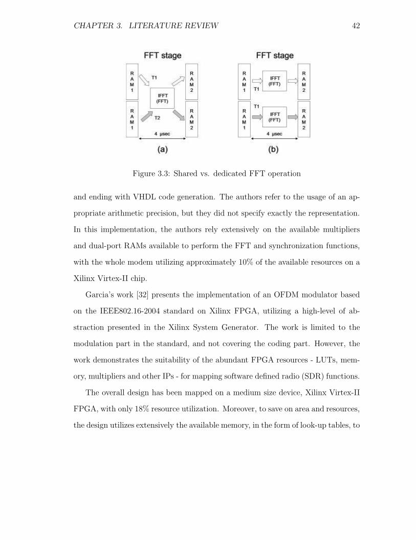
In [30], the work by Park et al. presents a prototype of the implementation of the
PHY layer of a (Multiple-Input-Multiple-Output-OFDM) MIMO-OFDM system

CHAPTER 3. LITERATURE REVIEW 41
on FPGA. The work furthermore emphasizes on the pipelined architecture using
a shared FFT between the modulation chains in the system as seen in Figure 3.3.
This has proved a 30% saving in the area, while achieving the same data rate
for what is noted by the authors as the baseline MIMO-OFDM implementation.
The other feature emphasized on is the dynamic configuration. In order to satisfy
the standard requirements number of blocks in the system - coding, mapping and
parsing - have to be dynamically configured. The main contribution is attributed to
the study of the effect of using only one Radix-4 FFT processor or Radix-2 pipelined
streaming FFT processor, instead of using as many FFT processors as the number
of antennas in MIMO systems, 802.11n and 802.16 standards. The design revolves
around the pipelined architecture of the FFT block, where the path is divided into
three phases: storing the I/Q pairs into the two block RAMs as an input to the
FFT processor; the FFT stage; and out-stage where the FFT output is stored in
one of the available output RAMs to be processed further. The authors show how
this architecture could be mapped on an FPGA with a 30% saving. Furthermore,
the authors provide a baseline for the complexity of computational operations and
their level of abstraction for each block in the receiving and transmitting sides,
where they claim that maximum number of operations for a 2*2 MIMO-OFDM
system requires 13092 MOPS that are not supported by a single DSP ship.
The work by Manavi and Shayan in [31] presents the complete design of the
802.11a PHY layer on FPGAs, and it includes also the synchronization function-
ality. The implementation is based on the design flow starting from the floating-
point modeling, simulation and verification, going through fixed-point translation
CHAPTER 3. LITERATURE REVIEW 42
Figure 3.3: Shared vs. dedicated FFT operation
and ending with VHDL code generation. The authors refer to the usage of an ap-
propriate arithmetic precision, but they did not specify exactly the representation.
In this implementation, the authors rely extensively on the available multipliers
and dual-port RAMs available to perform the FFT and synchronization functions,
with the whole modem utilizing approximately 10% of the available resources on a
Xilinx Virtex-II chip.
Garcia’s work [32] presents the implementation of an OFDM modulator based
on the IEEE802.16-2004 standard on Xilinx FPGA, utilizing a high-level of ab-
straction presented in the Xilinx System Generator. The work is limited to the
modulation part in the standard, and not covering the coding part. However, the
work demonstrates the suitability of the abundant FPGA resources - LUTs, mem-
ory, multipliers and other IPs - for mapping software defined radio (SDR) functions.
The overall design has been mapped on a medium size device, Xilinx Virtex-II
FPGA, with only 18% resource utilization. Moreover, to save on area and resources,
the design utilizes extensively the available memory, in the form of look-up tables, to

CHAPTER 3. LITERATURE REVIEW 43
replace other expensive blocks. For example, the mapper design is based on storing
the normalized values of the I and Q values in a look-up table (ROM) to avoid the
introduction of a multiplier. The work also specifies the arithmetic representation
to be a 10-bit signed fixed point representation on all blocks, except the FFT that
produces 16-bit vectors. The authors did not present any results on how they have
selected this word length, instead they rely on previous work by Gifford et al. [33].
3.2.2 ASIPs
The work by Kim and Sunwoo, [34], presents three ASIPs, and one of them targets
SoC implementation of an OFDM signal processor. The work proposes an ASIP
that performs the main OFDM functions through introducing specific instructions
for each OFDM function. For example, the authors claim that the proposed ASIP
design requires only three instructions to perform the FFT computation. However,
no details are provided. Furthermore, the processor contains specific instructions
grouped in the bit-manipulation-unit (BMU) to perform the coding functions (con-
volutional encoding, puncturing and interleaving).
The presented results describe a processor operating at a maximum frequency of
280 MHz and a total of 107,000 gates using the SEC 0.18 µm standard cell library.
Furthermore, the presented results show a speed-up factor that ranges between 1.25
and 2 in the number of cycles required to perform the FFT function when compared
to the Camel DSP and TI 62X processor, while the design does not outperform the
DSP24 processor. The authors also claim that a 2x and 3x speed-up factors are
achieved in the BMU functions. Finally, the work does not provide any comments
CHAPTER 3. LITERATURE REVIEW 44
on power consumptions or any comparison figures to similar ASIC designs.
Another work by Quax et al., [35], presents an ASIP design for a multistan-
dard FFT processor for Wireless communications. The work looks specifically at
the WPAN IEEE 802.15.3a standard, yet it generalizes the results for another
OFDM-based standards (WiFi and WiMAX). The implementation is based on the
proprietary design methodology by Silicon Hive [36], which is based on a basic
configurable component referred to as the processing and storage element (PSE).
The PSE is a configurable unit that consists of a number of functional units, regis-
ter files, interconnect networks and an optional memory element. The processors is
generated automatically based on hardware description through a highly abstracted
HDL named TIM. The results obtained by the authors show that the proposed ASIP
has outperformed a comparable ASIC design in terms of area, which may not be
accurate enough due to the technology difference, since the ASIC design is based on
the 0.18 µm technology while the authors’ work is based on the 0.12 µm technology.
Furthermore, the power dissipation figure obtained does not represent a candidate
figure for mobile devices with a peak power consumption of 1.78 W. However, the
design presents a very scalable design that can scale up to 1024-point FFT proces-
sor, and also a conformance to the timing constraint of 312.5 ns operating at 336
MHz.
In [21], Lee et al. study the implementation of an OFDM transceiver on an
Application-specific DSP (AS-DSP). The design targets an improvement in the
number of cycles required to perform the OFDM blocks’ tasks in other DSP chips.
The comparison shows that an improvement of 10% over the Carmel DSP and
CHAPTER 3. LITERATURE REVIEW 45
30% over the TI TMS320C62X was achieved, considering the most computationally
demanding block, FFT. The proposed design has demonstrated that only 390 cycles
are required to perform a 64-point FFT, which correspond to 1.4 µsec computation
time. As an estimation for the 802.16 standard, this will require 7.3 µsec, which is
still within the timing constraint of 72 µsec symbol time. The authors work showed
that an AS-DSP with a total gate count of 80K gates using 0.18 µm technology
and operating at 280 MHz frequency was able to accommodate the FFT function
in OFDM systems. The design provides a compromise between the traditional DSP
chips and conventional ASIC FFT processor, where it provides faster design than
other DSP chips and maintaining flexibility in supporting FFT transforms with
64 to 8192 point. However, since the suggested AS-DSP design utilizes radix-2
computation, while ASIC FFT processors utilizes radix-4 computations, it is still
expected that ASIC FFT processors will outperform the suggested AS-DSP chip.
An industrial contribution by stretch Inc. [37] shows the capability of software-
configurable processors to accommodate a cost-effective and time-saving implemen-
tation of the IEEE802.16 standard. The platform merges the HW and SW devel-
opment utilizing the C-language for accelerating the computationally demanding
blocks; such as FFT and Viterbi encoder, using instruction extension. The pro-
cessors proposed by Stretch, Inc. (S5000 and S6000) are based on the Tensilica
Xtensa RISC and XL processor cores [13] and the Stretch Instruction Set Exten-
sion Fabric (ISEF). The demonstration provided by Stretch implements a base
station and a CPE that contain both the MAC and PHY and the Ethernet stack
for the IEEE802.16-2004 standard with number of cycles equal to 76 Mcycles/sec

CHAPTER 3. LITERATURE REVIEW 46
in the receiver side and 16 Mcycles/sec at the transmitter side for 16 and 64-QAM
modulation and 3/4 coding rate. The implementation addresses issues such as
the run-time configuration capability, the use of wide registers that added a 28%
performance improvement in computing a Radix-4 FFT. This comes through a
specifically extended ISEF that passes 3 sets of 4 complex values. Moreover, the
software-configurable processors benefit from their capability in performing bit-
level operations, where GPP lacks. This means the readiness of such processors to
fit for the needs of WiMAX implementations where it requires both bit-level and
block-level operations.
As presented above, the promises of FPGAs and reconfigurable architectures are
remarkable. The flexibility and the available computational power pave the way
for these architectures to get a big share in the development and implementation of
OFDM-based systems. The studies show the capability of FPGAs to accommodate
different wireless standards; e.g. 802.11a and 802.16. Moreover, this proves the
readiness of these platforms to adopt the emerging techniques that supports more
complex and high data rate systems, such as MIMO-OFDM. Configurable proces-
sors promise to provide the capability of a lower cost and fast implementations,
with lower power and area requirements. However, due to the complexity of the
newly proposed standards, most of the published works limit themselves to certain
functions in the chain of an OFDM-based system. Therefore, our work looks at
implementing a complete OFDM-based systems based on the 802.16 standard, and
this includes both the coding and modulation part.

CHAPTER 3. LITERATURE REVIEW 47
3.3 Summary
The studies presented in this chapter describe the contribution made in imple-
menting OFDM-based systems using: pure software, ASIC-based or reconfigurable
computing systems. The work targeting software implementations, showed the
difficulty of these platforms to provide high performance design and low power
consumption, but with the higher flexibility among all approaches. On the other
hand, ASIC implementations provide fixed designs that are higher in performance,
but due to complexity, few studies are focusing on the complete implementation.
Moreover, the inflexible nature of those designs makes them unsuitable for evolving
standards, as well as being expensive for low volume productions. The third ap-
proach represented by reconfigurable platforms, in specific FPGAs, demonstrates
the capability of a compromise between a flexible and high performance implemen-
tation. Even though, issues such as power consumption and area might still restrict
FPGAs from invading markets of small-portable-battery-powered devices.
In implementing OFDM-based systems, specifically the IEEE 802.16 standard,
most of the published work focuses on certain functions and not covering the com-
plete chain. Moreover, while certain studies focus on FPGAs, others focus on
software-configurable processors. This brings the attention to prove the capabil-
ity of these platforms to accommodate complex standards such as WiMAX, where
they both promise flexibility, high performance and fast design time. Furthermore,
investigating different design approaches is also desirable, since no previous work
provided the different trade-offs associated with the implementation of OFDM-
based systems on RCS.

Chapter 4
Methodology
The main objective of this chapter is to discuss the overall methodology used
in this thesis and introduce the implementation approaches employed to translate
the IEEE 802.16-2004 standard and map it on a reconfigurable computing sys-
tems (RCS). As stated in Chapters 2 and 3, RCS are considered as a viable option
for mapping wired and wireless communication standards based on OFDM. Our
goal here is to demonstrate reconfigurable computing systems capabilities and the
significant implementation approaches highlighting their main advantages and dis-
advantages. Therefore, to compare the different available approaches, the research
focuses on implementing the standard using three approaches by targeting Xilinx
medium size FPGAs [38] and the Tensilica Xtensa configurable processors [13].
The first approach is at a low level of abstraction, while the second and the third
approaches utilize a high level language/modeling system.
In the first approach, a hardware description language, namely VHDL, was
used to translate the different standard functions/blocks into synthesizable VHDL
48
CHAPTER 4. METHODOLOGY 49
Intellectual Properties (IPs) cores. The Xilinx Integrated Software Environment
(ISE), [38], tool was used to develop pure VHDL IPs and also utilize some of the
off-the-shelf IPs found in the Xilinx IP core library. The second approach utilizes a
MATLAB-based system that accelerates DSP systems design. The systems is able
to translate a MATLAB written code into an HDL code, VHDL or Verilog, ready
to be synthesized and mapped onto an FPGA fabric. The third approach targets
tailoring the Tensilica Xtensa processor instruction set to speed-up the C/C++
original code. The approach utilizes the Tensilica integrated development environ-
ment (Xtensa Xplorer) to write the original C code, and to modify the instruction
set and configure the processor. The objective is to compare the employed ap-
proaches in terms of area, performance, power and design time.
4.1 Protocol Stack and Scope of Work
The IEEE 802.16-2004 defines both the Medium Access Control (MAC) and Phys-
ical (PHY) layers, while the WiMAX forum defines the WiMAX Network compo-
nents and the different deployment architectures. The MAC layer is composed of 3
sublayers with different functionalities, while the PHY layer is responsible for the
digital signal processing and radio frequency interface. In this work, we limit the
implementation to the OFDM functions of the digital baseband processing part of
the PHY layer, which does not include any burst formation. It starts with data
randomization and terminates by performing cyclic prefix insertion. The design
also limits the coding stage to the main blocks, not taking into consideration the
optional coding blocks: block turbo codes, convolutional turbo codes, and low den-
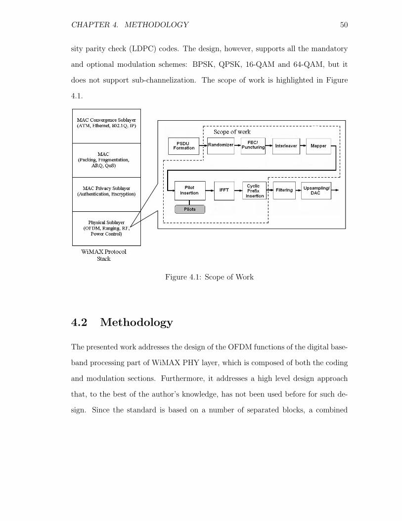
CHAPTER 4. METHODOLOGY 50
sity parity check (LDPC) codes. The design, however, supports all the mandatory
and optional modulation schemes: BPSK, QPSK, 16-QAM and 64-QAM, but it
does not support sub-channelization. The scope of work is highlighted in Figure
4.1.
Figure 4.1: Scope of Work
4.2 Methodology
The presented work addresses the design of the OFDM functions of the digital base-
band processing part of WiMAX PHY layer, which is composed of both the coding
and modulation sections. Furthermore, it addresses a high level design approach
that, to the best of the author’s knowledge, has not been used before for such de-
sign. Since the standard is based on a number of separated blocks, a combined
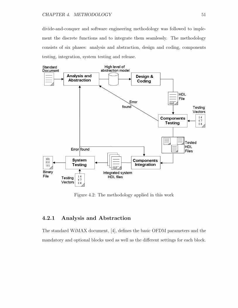
CHAPTER 4. METHODOLOGY 51
divide-and-conquer and software engineering methodology was followed to imple-
ment the discrete functions and to integrate them seamlessly. The methodology
consists of six phases: analysis and abstraction, design and coding, components
testing, integration, system testing and release.
Figure 4.2: The methodology applied in this work
4.2.1 Analysis and Abstraction
The standard WiMAX document, [4], defines the basic OFDM parameters and the
mandatory and optional blocks used as well as the different settings for each block.
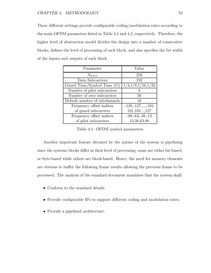
CHAPTER 4. METHODOLOGY 52
These different settings provide configurable coding/modulation rates according to
the main OFDM parameters listed in Table 4.1 and 4.2, respectively. Therefore, the
higher level of abstraction model divides the design into a number of consecutive
blocks, defines the level of processing of each block, and also specifies the bit width
of the inputs and outputs of each block.
Parameter Value
NFFT 256Data Subcarriers 192
Guard Time/Symbol Time (G) 1/4,1/8,1/16,1/32Number of pilot subcarriers 8Number of zero subcarriers 56
Default number of subchannels 16Frequency offset indices -128,-127,...,-101
of guard subcarriers 101,102...,127Frequency offset indices -88,-63,-38,-13
of pilot subcarriers 13,38,63,88
Table 4.1: OFDM symbol parameters
Another important feature dictated by the nature of the system is pipelining
since the systems blocks differ in their level of processing; some are either bit-based,
or byte-based while others are block-based. Hence, the need for memory elements
are obvious to buffer the following frame results allowing the previous frame to be
processed. The analysis of the standard document mandates that the system shall:
• Conform to the standard details.
• Provide configurable IPs to support different coding and modulation rates.
• Provide a pipelined architecture.
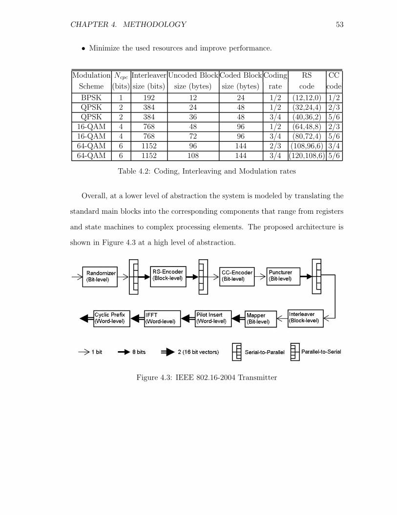
CHAPTER 4. METHODOLOGY 53
• Minimize the used resources and improve performance.
Modulation Ncpc Interleaver Uncoded Block Coded Block Coding RS CC
Scheme (bits) size (bits) size (bytes) size (bytes) rate code code
BPSK 1 192 12 24 1/2 (12,12,0) 1/2QPSK 2 384 24 48 1/2 (32,24,4) 2/3QPSK 2 384 36 48 3/4 (40,36,2) 5/6
16-QAM 4 768 48 96 1/2 (64,48,8) 2/316-QAM 4 768 72 96 3/4 (80,72,4) 5/664-QAM 6 1152 96 144 2/3 (108,96,6) 3/464-QAM 6 1152 108 144 3/4 (120,108,6) 5/6
Table 4.2: Coding, Interleaving and Modulation rates
Overall, at a lower level of abstraction the system is modeled by translating the
standard main blocks into the corresponding components that range from registers
and state machines to complex processing elements. The proposed architecture is
shown in Figure 4.3 at a high level of abstraction.
Figure 4.3: IEEE 802.16-2004 Transmitter

CHAPTER 4. METHODOLOGY 54
4.2.2 Design and Coding
Designing for FPGA has different flavors. In Chapter 5, a low level approach is
used where the whole digital baseband processing part of both the transmitting and
the receiving chains are coded in VHDL. The second approach utilizes MATLAB
code written to target hardware where certain features available in the MATLAB
libraries are not fully supported to be synthesized. Chapter 6 discusses in more
detail the AccelDSP tool, [38], highlighting its advantages and disadvantages. In
designing each block, the behavior of these blocks tend to rely on mapping the
input values to a predefined constants. In another case, the input data have to
be stored and manipulated according to certain indexing scheme. Based on these
observations, it was concluded that memory elements, RAMs and ROMs, will be
the primary resource for most of the processing elements.
4.2.3 Testing and Integration
To ensure conformance, testing has to be performed on each block individually
and on the complete system after integrating the different blocks. Testing vectors
provided in the standard document are the main testbench used at the block and
system level. The testing vectors show the input and the output for each block. To
further test the system, a closed loop of the transmitter and the receiver provides
a testing facility.
Further verification utilized the HW-Cosim technique where the test benches
were used to drive the circuit after being mapped on the targeted FPGA. The
AccelDSP and System Generator tools were used for that purpose, while for the
CHAPTER 4. METHODOLOGY 55
Tensilica Xtensa approach testing was based only on the simulation results inside
the Xtensa Xplorer tool.
The other important step in the design process is the integration of the differ-
ent blocks that were tested individually to eventually form the transmitting and
receiving chains. Following the integration, testing for the complete system was
performed, and any faults found would require an iterative process of reviewing
the individual block design and retesting the system. Verification of the complete
design should lead to the releasing step, where the complete system design is ready
to be mapped.
4.3 Design Environment
In this section, the design environments for the three approaches are presented. For
the first approach, the Xilinx Integrated Software Environment (ISE) version 8.2
was used for design entry, synthesis and mapping. The Xilinx ISE simulator was
used to verify the design at both the component level and the system level. The ISE
was installed on a IBM workstation running MS Windows XP with service pack
2. For the second approach, the AccelDSP software provided by Xilinx was used
for coding, while debugging was performed in MATLAB. Synthesizing, mapping
and implementing the design on the FPGA chip was performed through interfacing
AccelDSP to the Xilinx ISE flow. For simulation, the ModelSim Starter Edition
was interfaced to the AccelDSP, with the results being viewed inside the AccelDSP.
The same machine was used to run the AccelDSP software.
For the ASIP approach, the Tensilica Integrated Development Environment

CHAPTER 4. METHODOLOGY 56
Xtensa Xplorer CE was the main tool, where all the coding, configuration, profiling
and testing was performed within it. The Xtensa Xplorer IDE is based in part on
the open-source ECLIPSE platform for tool integration, and it works as a collection
of SOC design tools that includes software development and processor configuration
into one common platform.
4.4 Summary
The OFDM functions of the digital baseband processing part of the PHY layer of the
IEEE 802.16-2004 standard are targeted in this work. The methodology followed
in this work divides the design into different components, coding and verifying each
component and finally integrating the complete system. Two different platforms
are targeted: the Xilinx FPGA and the Tensilica Xtensa configurable processors.
Furthermore, two different design flows, based on software tools provided by Xilinx
Inc., were selected to tackle the two approaches that are targeting Xilinx FPGAs.

Chapter 5
Custom RTL Implementation
This chapter discusses the custom RTL implementation approach employed in
this thesis work to translate the IEEE 802.16-2004 standard and map it on an
FPGA. This approach is at a low level of abstraction, where a hardware descrip-
tion language, namely VHDL [39], was used to translate the different standard
functions/blocks into a synthesizable core. The Xilinx Integrated Software Envi-
ronment (ISE), [38], tool was used to develop pure VHDL IPs and also utilize some
of the off-the-shelf IPs found in the Xilinx IP core library. This approach aims
at translating the standard details into a pure VHDL presentation with the aid
of off-the-shelf IPs available. The methodology discussed in Chapter 4 is applied,
where the different functions coded in VHDL and the available IPs were wrapped
to combine the transmitting and receiving chains. The design environment was
based on the Xilinx Integrated Software Environment (ISE v8.2), where all the
steps (coding, testing and integration) were performed by the same tool. In this
approach, both the transmitting and the receiving chains were implemented, but
57

CHAPTER 5. CUSTOM RTL IMPLEMENTATION 58
restricting it only to the mandatory functions of the standard.
5.1 Transmitter Design Details
In the following subsections, each of the standard functions/blocks of the transmit-
ting chain will be presented, and the main design features will be highlighted. The
receiving chain will be discussed briefly in section 5.2, since most of the blocks are
simply performing the reverse function for its corresponding block on the transmit-
ting side.
5.1.1 Randomization
The goal of this phase is to shuffle the input data on each burst to avoid long
sequence of zeros and ones, and to provide a layer1 encryption scheme. The block
manipulates the data at the bit level, where it processes the input data bytes bit
by bit, MSB first. This is implemented with a Pseudo Random Binary Sequence
(PRBS) generator that utilizes a 15 bit linear feedback shift register LFSR to
represent the generator polynomial of (1+x14+x15), and in the feedback branch two
2-input XOR gates are used as shown in Figure 5.1. According to the specification
of the standard, the randomizer requires initialization per each burst, with the
initializing vectors indicated in Figure 5.1. BSID refers to base station ID, DIUC is
the downlink interval usage code, while Frame No. indicates the number assigned
to the current frame.
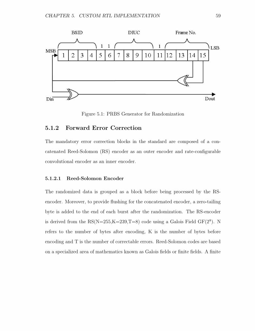
CHAPTER 5. CUSTOM RTL IMPLEMENTATION 59
Figure 5.1: PRBS Generator for Randomization
5.1.2 Forward Error Correction
The mandatory error correction blocks in the standard are composed of a con-
catenated Reed-Solomon (RS) encoder as an outer encoder and rate-configurable
convolutional encoder as an inner encoder.
5.1.2.1 Reed-Solomon Encoder
The randomized data is grouped as a block before being processed by the RS-
encoder. Moreover, to provide flushing for the concatenated encoder, a zero-tailing
byte is added to the end of each burst after the randomization. The RS-encoder
is derived from the RS(N=255,K=239,T=8) code using a Galois Field GF(28). N
refers to the number of bytes after encoding, K is the number of bytes before
encoding and T is the number of correctable errors. Reed-Solomon codes are based
on a specialized area of mathematics known as Galois fields or finite fields. A finite

CHAPTER 5. CUSTOM RTL IMPLEMENTATION 60
field has the property that arithmetic operations (+,-,x,/ etc.) on field elements
always have a result in the field. A Reed-Solomon encoder or decoder needs to
carry out these arithmetic operations. These operations require special hardware
or software functions to be implemented.
A Reed-Solomon codeword is generated using a special polynomial. All valid
codewords are exactly divisible by the generator polynomial. The general form of
the generator polynomial is g(x) = (x−αi)(x−αi+1)...(x−αi+2t), and the codeword
is constructed using c(x) = g(x).i(x). Where g(x) is the generator polynomial, i(x)
is the information data and c(x) is the codeword. To support variable block size and
therefore configurable error correction capability, puncturing and shortened codes
are supported. Finally, in the IEEE802.16-2004 standard the redundant bytes are
sent first, while leaving the tailing byte at the end to flush the convolutional encoder
stage.
In implementing the RS-encoder, the RS-encoder IP provided by the Xilinx
core generator library was used. The used IP is a general RS-encoder, with no
puncturing and shortening support. To mitigate this, two stages (pre and post RS-
encoding) where used to wrap the RS-encoder IP. The first stage (pre-RS) provides
the functions of zero tailing and shortened codes capability. This is implemented
as a RAM preinitialized to zero values, the actual data is stored in locations 239-K’
to 238, where K’ represents the shortened code. The second stage provides the
capability of extracting the first 2T’ parity bytes that has to be forwarded to the
next stage out of the original 2T=16 bytes, and extracting the shortened K’ bytes
out of the 239 bytes to form the N’ block (N ′ = K ′+2T ′). In addition, the post-RS

CHAPTER 5. CUSTOM RTL IMPLEMENTATION 61
Figure 5.2: RS Encoder Stages
stage provides the capability to reorder the output bytes, so the parity bytes are
stored at the top of the RAM used for this stage, while the rest are stored starting
from location 2T’. Both stages were built based on the available block RAMs with
duplication. This duplication will guarantee pipelining, since the randomization
and the convolutional encoding stages are based on a bit-level processing, while the
processing of the RS-encoding stage is block-based. The stages of the RS-encoding
are illustrated in Figure 5.2.
5.1.2.2 Convolutional Encoder
The inner part of the FEC block is based on a binary convolutional encoder, shown
in Figure 5.3. The encoder is based on a native encoding rate of 1/2, with a
constraint length of 7. The 1/2 encoding rate means that for every input bit two

CHAPTER 5. CUSTOM RTL IMPLEMENTATION 62
output bits are produced, and these output bits are produced using the generator
ploynominals given by Equations (5.1) and (5.2)
G1 = 1718, forXoutput (5.1)
G2 = 1338, forY output (5.2)
Figure 5.3: Convolutional Encoder of rate 1/2
To save on bandwidth, the encoder is followed by a puncturing stage that allows
variable and less redundant coding rates of 2/3, 3/4 and 5/6, according to Table 5.1.
The 1’s in the table denote that the corresponding convolutional encoder output is
passed, while 0’s denote they are not used. The straightforward implementation of
the convolutional encode is represented by a number of delay elements (D-type flip
flops) and two XOR gates to implement the modulo-2 adder and construct the two
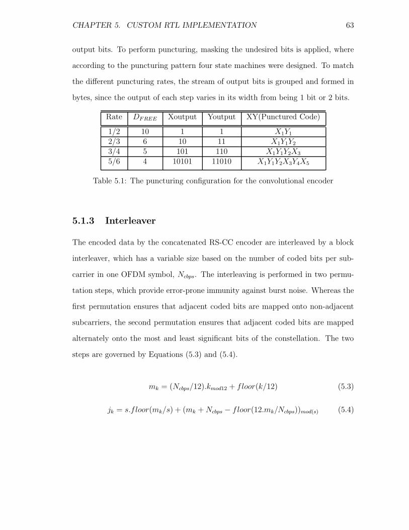
CHAPTER 5. CUSTOM RTL IMPLEMENTATION 63
output bits. To perform puncturing, masking the undesired bits is applied, where
according to the puncturing pattern four state machines were designed. To match
the different puncturing rates, the stream of output bits is grouped and formed in
bytes, since the output of each step varies in its width from being 1 bit or 2 bits.
Rate DFREE Xoutput Youtput XY(Punctured Code)
1/2 10 1 1 X1Y1
2/3 6 10 11 X1Y1Y2
3/4 5 101 110 X1Y1Y2X3
5/6 4 10101 11010 X1Y1Y2X3Y4X5
Table 5.1: The puncturing configuration for the convolutional encoder
5.1.3 Interleaver
The encoded data by the concatenated RS-CC encoder are interleaved by a block
interleaver, which has a variable size based on the number of coded bits per sub-
carrier in one OFDM symbol, Ncbps. The interleaving is performed in two permu-
tation steps, which provide error-prone immunity against burst noise. Whereas the
first permutation ensures that adjacent coded bits are mapped onto non-adjacent
subcarriers, the second permutation ensures that adjacent coded bits are mapped
alternately onto the most and least significant bits of the constellation. The two
steps are governed by Equations (5.3) and (5.4).
mk = (Ncbps/12).kmod12 + floor(k/12) (5.3)
jk = s.f loor(mk/s) + (mk + Ncbps − floor(12.mk/Ncbps))mod(s) (5.4)
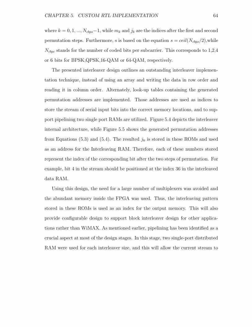
CHAPTER 5. CUSTOM RTL IMPLEMENTATION 64
where k = 0, 1, ..., Ncbps−1, while mk and jk are the indices after the first and second
permutation steps. Furthermore, s is based on the equation s = ceil(Ncbps/2),while
Ncbpc stands for the number of coded bits per subcarrier. This corresponds to 1,2,4
or 6 bits for BPSK,QPSK,16-QAM or 64-QAM, respectively.
The presented interleaver design outlines an outstanding interleaver implemen-
tation technique, instead of using an array and writing the data in row order and
reading it in column order. Alternately, look-up tables containing the generated
permutation addresses are implemented. Those addresses are used as indices to
store the stream of serial input bits into the correct memory locations, and to sup-
port pipelining two single port RAMs are utilized. Figure 5.4 depicts the interleaver
internal architecture, while Figure 5.5 shows the generated permutation addresses
from Equations (5.3) and (5.4). The resulted jk is stored in these ROMs and used
as an address for the Interleaving RAM. Therefore, each of these numbers stored
represent the index of the corresponding bit after the two steps of permutation. For
example, bit 4 in the stream should be positioned at the index 36 in the interleaved
data RAM.
Using this design, the need for a large number of multiplexers was avoided and
the abundant memory inside the FPGA was used. Thus, the interleaving pattern
stored in these ROMs is used as an index for the output memory. This will also
provide configurable design to support block interleaver design for other applica-
tions rather than WiMAX. As mentioned earlier, pipelining has been identified as a
crucial aspect at most of the design stages. In this stage, two single-port distributed
RAM were used for each interleaver size, and this will allow the current stream to
CHAPTER 5. CUSTOM RTL IMPLEMENTATION 65
Figure 5.4: Interleaver internal architecture
Figure 5.5: Permutation table contents (case of 192 bits interleaver size)

CHAPTER 5. CUSTOM RTL IMPLEMENTATION 66
be read from while the second is used to store the incoming bit stream.
5.1.4 Constellation Mapper
The interleaved bits are serially fed to the constellation mapper to produce the
corresponding Inphase and Quadrature (I/Q) pairs. The mapper supports the
BPSK, QPSK, 16-QAM and 64-QAM modulation schemes. The mapped data is
normalized by multiplying it with a factor c, thus equal average power is achieved
for the generated symbols. The constellation mapped data are assigned to the
allocated data subcarriers of the OFDM symbol in the order of the increasing
frequency offset, where the first mapped data is allocated to the subcarrier with
the lowest frequency offset index.
Since each scheme maps a group of 1,2,4 or 6 bits into the corresponding I/Q
pairs, the mapper receives the serial input stream and groups them into chunks of
1,2,4 or 6 bits, referred in the standard as Ncpc. These bits are used to index a ROM-
based look-up table that contains the corresponding I/Q pairs values. The mapper
is implemented with 4 ROMs, one for each modulation scheme.To facilitate the
design, each chunk of Ncpc is divided into two parts to address two separate ROMs,
one contains the I values while the other contains the Q values. The values stored
are normalized by the factor c to avoid introducing multipliers after the mapping.
The normalized values are stored in a signed fixed point representation of 16 bits and
decimal point at 14. This was selected since all values are less than zero, except
the BPSK values that could be either 1 or -1. Thus, only two bits are required
to represent the sign and the other 14 bits are used to represent the fractional
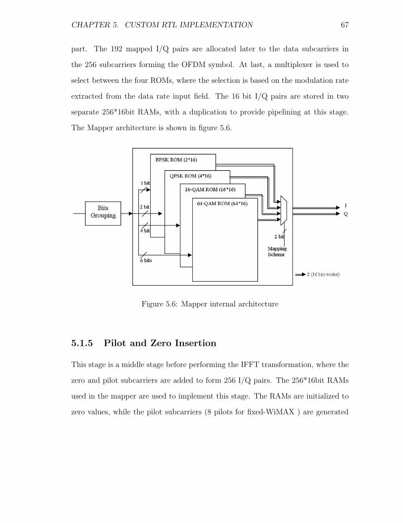
CHAPTER 5. CUSTOM RTL IMPLEMENTATION 67
part. The 192 mapped I/Q pairs are allocated later to the data subcarriers in
the 256 subcarriers forming the OFDM symbol. At last, a multiplexer is used to
select between the four ROMs, where the selection is based on the modulation rate
extracted from the data rate input field. The 16 bit I/Q pairs are stored in two
separate 256*16bit RAMs, with a duplication to provide pipelining at this stage.
The Mapper architecture is shown in figure 5.6.
Figure 5.6: Mapper internal architecture
5.1.5 Pilot and Zero Insertion
This stage is a middle stage before performing the IFFT transformation, where the
zero and pilot subcarriers are added to form 256 I/Q pairs. The 256*16bit RAMs
used in the mapper are used to implement this stage. The RAMs are initialized to
zero values, while the pilot subcarriers (8 pilots for fixed-WiMAX ) are generated

CHAPTER 5. CUSTOM RTL IMPLEMENTATION 68
based on PRBS generator given by the polynomial (X11 + X9 + 1) and depicted in
Figure 5.7. The PRBS generates a sequence (wk) that is used to derive the pilot
modulation value. Depending on its frequency offset index, each pilot is derived
using BPSK modulation according to Equations (5.5) and (5.6).
DL : c−88 = c−38 = c63 = c88 = 1 − 2wk, c−63 = c−13 = c13 = c38 = 1 − 2w̄k (5.5)
UL : c−88 = c−38 = c13 = c38 = c63 = c88 = 1 − 2wk, c−63 = c−13 = 1 − 2w̄k (5.6)
Figure 5.7: PRBS generator for pilot generation
The generated pilots are stored in the memory locations, in hexadecimal, (27,
40, 59, 72, 8C, A5, BE, D7) which correspond to frequency offset indexes (-88, -63,
-38, -13, 13, 38, 63, 88). The mapped I/Q pairs from the mapper stage are also

CHAPTER 5. CUSTOM RTL IMPLEMENTATION 69
stored in their corresponding memory locations that reflects their frequency offset
indexes as per Table 4.1.
5.1.6 IFFT
The 256 I/Q pairs generated are fed to the Inverse Fast Fourier Transform (IFFT)
module. 265-point IFFT is used at the transmitter side to transform the sub-carriers
from the frequency domain to the time domain. At the receiver side, an FFT is used
to transform back the time domain sub-carriers into the frequency domain. This
block was one of the few main blocks not designed in VHDL by the author, where
the Intellectual Property (IP) core available in the Xilinx development environment
(ISE) was utilized. The generated IP was based on continuous processing of the
arriving data instead of working on the whole symbol samples all at once. This
capability came from the pipelining provided by the previous and the following
stages, where each generated I/Q pair in the I/Q bank is fed to the IFFT processor.
Next, after the required number of cycles by the IFFT block, the generated real
and imaginary pairs are forwarded to the CP block. The IP contains an address
generator to index external memory of both the input and the output, and those
addresses are used to index the RAMs utilized by the mapper stage and the RAMs
in the following stage, the cyclic prefix insertion stage.
5.1.7 Cyclic Prefix Insertion
Cyclic Prefix (CP) is the replication of the last L samples of the OFDM symbol
to overcome issues such as ISI and ICI. In the 802.16-2004 standard, the last (n)
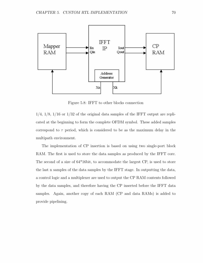
CHAPTER 5. CUSTOM RTL IMPLEMENTATION 70
Figure 5.8: IFFT to other blocks connection
1/4, 1/8, 1/16 or 1/32 of the original data samples of the IFFT output are repli-
cated at the beginning to form the complete OFDM symbol. These added samples
correspond to τ period, which is considered to be as the maximum delay in the
multipath environment.
The implementation of CP insertion is based on using two single-port block
RAM. The first is used to store the data samples as produced by the IFFT core.
The second of a size of 64*16bit, to accommodate the largest CP, is used to store
the last n samples of the data samples by the IFFT stage. In outputting the data,
a control logic and a multiplexer are used to output the CP RAM contents followed
by the data samples, and therefore having the CP inserted before the IFFT data
samples. Again, another copy of each RAM (CP and data RAMs) is added to
provide pipelining.
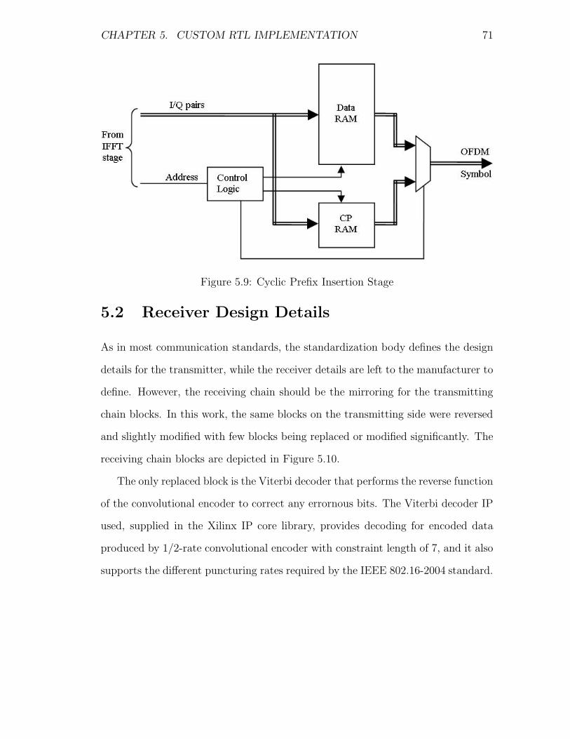
CHAPTER 5. CUSTOM RTL IMPLEMENTATION 71
Figure 5.9: Cyclic Prefix Insertion Stage
5.2 Receiver Design Details
As in most communication standards, the standardization body defines the design
details for the transmitter, while the receiver details are left to the manufacturer to
define. However, the receiving chain should be the mirroring for the transmitting
chain blocks. In this work, the same blocks on the transmitting side were reversed
and slightly modified with few blocks being replaced or modified significantly. The
receiving chain blocks are depicted in Figure 5.10.
The only replaced block is the Viterbi decoder that performs the reverse function
of the convolutional encoder to correct any errornous bits. The Viterbi decoder IP
used, supplied in the Xilinx IP core library, provides decoding for encoded data
produced by 1/2-rate convolutional encoder with constraint length of 7, and it also
supports the different puncturing rates required by the IEEE 802.16-2004 standard.

CHAPTER 5. CUSTOM RTL IMPLEMENTATION 72
Figure 5.10: Receiver Block Diagram
The depuncturing was implemented here as an external unit to the Viterbi decoder
IP. This was chosen to avoid replicating the Viterbi decoder IP for the different
rates needed. Furthermore, an input-bits widening unit was added to support the
3-bit width of the Viterbi decoder required to support soft decision coding, since
1-bit hard decision coding does not support puncturing.
Another block that was significantly modified was the CP removing stage, where
no BRAM was required. The unit works by reading the stream of I/Q pairs and
ignoring the first 128,64,16 or 8 samples, while the rest are forwarded directly to the
FFT stage. Hence, there is no need to buffer the I/Q pairs using BRAMs as in the
transmitting side, where reordering or replication of the last n samples mandates
the existence of BRAMs. The other block significantly modified is the demapper,
where a buffering stage is added before the demapped bits are deinterleaved. This
is due to the demapper internal functionality where it produces different bit-width
output (1,2,4 or 6) depending on the modulation scheme. The demapped bits are
grouped in words of 12 bits in width and stored in a RAM. The demapper internal

CHAPTER 5. CUSTOM RTL IMPLEMENTATION 73
architecture is depicted in figure 5.11.
Figure 5.11: Demapper internal architecture
The rest of the blocks are mainly based on the IPs developed for the transmitter
with slight modification. More accurately, one block, the randomizer/derandomizer,
is the same IP used, but with a different initialization vector used for the DL
and UL. The other block is the deinterleaver, where the only modified part is
the contents of the 4 ROMS (look-up tables) to reflect the indices generated by
Equations (5.7) and (5.8). The other blocks, such as the FFT and the RS decoder,
are generated through the Xilinx IP core library and slight modifications were
needed to accommodate the differences between these IPs and the transmitting IPs.
In details, the pre-RS stage is not needed on the receiving side since no reordering
is needed. Even with all these stages that are omitted on the receiving side, the
complexity of the other blocks resulted that the receiver design will occupy more
area than the transmitter design.

CHAPTER 5. CUSTOM RTL IMPLEMENTATION 74
mj = s.f loor(j/s) + (j + floor(12.j/Ncbps))mod(s), j = 0, 1, ..., Ncbps − 1 (5.7)
kj = 12.mj − (Ncbps − 1).f loor(12.mj/Ncbps), j = 0, 1, ..., Ncbps − 1 (5.8)
5.3 Results
The implemented standard and the different IPs designed have been tested using
the testing vectors found in the standard document [4]. An example of these vectors
can be found in Appendix C. The testing, as per the followed methodology, was
performed at the component level first, and after the integration it was performed at
the system level. Early-found errors in the component design required remodeling
and redesigning, which saved time in the integration and system testing phases.
The testing results showed the conformance of all IPs designed to the standard
details, as well as the whole system. The system was designed, simulated and
verified in the Xilinx ISE v8.2, [38], installed on an IBM workstation running MS
Windows XP Service Pack 2. The design was mapped on a single Xilinx Virtex-II
Pro XV2P30-676-7c chip and reported approximately 50% resources utilization.
Upon the complete testing of each IP, the synthesis results were tabulized to
provide insight on the capability of FPGA-based platforms to accommodate such
designs. These results are listed in Table 5.2 to reflect the resources utilized per
IP in the transmitter and the receiver design, while the complete system design
is reported in Table 5.3. Moreover, the obtained results were compared to similar
CHAPTER 5. CUSTOM RTL IMPLEMENTATION 75
previous works [32] and [28].
5.3.1 Resource Utilization
It is obvious from the IPs resource utilization data, Table 5.2, that the most resource
demanding blocks are the FFT/IFFT block and the Viterbi decoder at the receiving
side. For example, the IFFT block occupation rate represents approximately 70%
of the total resources occupied by the transmitter design. On the receiving side,
both the FFT block and the Viterbi decoder block represent about 60% and 25%,
respectively, of the total number of resources required by the receiver design.
The remainder of the large blocks basically concentrate their occupation rate in
the number of block RAMs required, where 810 Kbits of the available 2,448 Kbits
are utilized. Moreover, it is also obvious the increased complexity of the receiver
design with an increase of 35% in the number of resources required by the transmit-
ter. Table 5.3 lists the required resources and the percentage of occupation when
the design is mapped on the Xilinx Virtex-II Pro FPGA (XV2P30-676-7c), where
the demand for the increased number of resources required by the receiver comes
from the Viterbi decoder. From the results, it is found that approximately half of
the FPGA resources are enough to accommodate most of the OFDM functions of
the PHY layer for a fixed WiMAX transceiver. Furthermore, both the demapper
and the RS-decoder utilize approximately double the size required by the mapper
and the RS-encoder. Otherwise, other blocks occupy roughly the same number of
resources on both the Tx and Rx sides, with a slight bigger size for the Rx IPs.
The only exception is the CP remove IP on the receiver side that occupies about a

CHAPTER 5. CUSTOM RTL IMPLEMENTATION 76
Unit (IP) #of
Slice
s
#of
Slice
FFs
#of
4-in
put
LU
Ts
#of
BR
AM
s
#of
MU
LT
18*1
8s
#of
GC
LK
s
Gat
eC
ount
Randomizer 49 68 56 - - 1 883RS-Encoder 304 308 534 4 - 2 268,091CC-Encoder 273 176 515 - - 2 4,322Interleaver 68 80 130 7 - 2 460,193Mapper 35 31 59 - - 1 631
Pilot Insert 53 34 95 4 - 1 262,974IFFT 2765 4067 4497 2 12 1 339,924
CP Insert 156 84 295 4 - 1 272,487
Derandomizer 49 68 56 - - 1 883RS-Decoder 604 769 1081 2 - 1 147,573VIT-Decoder 1527 1135 2481 5 - 2 363,930Deinterleaver 81 93 147 7 - 2 460,536Demapper 70 65 134 2 - 1 132,470
Pilot Remove 61 34 112 4 - 2 263,085FFT 2909 4280 4883 2 12 1 338,787
CP Remove 40 34 76 - - 1 749
Available Resources 13696 27392 27392 136 136 16 -
Table 5.2: Transmitter and Receiver IPs Resource Utilization
quarter of resources needed by the CP insert block on the transmitter side.
5.3.2 Timing Results
In addition to the amount of resources utilized, timing results form another impor-
tant dimension in FPGA-based designs. In this work, the main timing constraint
was to be able to produce one OFDM symbol in 72 µs. This requires the use of

CHAPTER 5. CUSTOM RTL IMPLEMENTATION 77
Resource Available Tx Rx TxRxResources used % used % used %
Slices 13696 3526 25 5195 38 8709 63Slice FFs 27392 4752 17 6385 23 11047 41
4-input LUTs 27392 5884 21 7705 28 13573 50Bonded IOBs 556 53 13 53 13 29 6
BRAMs 136 23 16 22 16 45 33MULT 136 12 8 12 8 24 16GCLKs 16 4 25 4 25 4 25
Table 5.3: Transceiver Resource Utilization
clock operating approximately at 14 MHz. The detailed timing results and maxi-
mum frequency of operation for each IP, for both the Tx and Rx chains, are listed
in Table 5.4. Furthermore, the same table shows also the timing results for the
complete Tx and Rx designs. It is clear from the results that the slowest IP man-
dates the minimum period and maximum frequency of operation for the complete
chain. In the Rx chain, the IFFT was the slowest with a minimum period of 5.821
ns, and a maximum frequency of operation of 171.804 MHz. On the other side, the
Rx chain, the slowest block is the Viterbi decoder with a minimum period of 5.155
ns and maximum frequency of operation of 193.971 Mhz.
5.3.3 Comparison
Few studies report the resources utilized in their WiMAX implementation on FP-
GAs. Two studies, [32] and [28], are compared to our current work. Firstly, since
Garcia’s work is limited only to the modulation part, the results obtained in this
work show a reasonable increase in the number of resources if the extra blocks
added are considered. Moreover, unlike Garcia’s work in which only the modula-

CHAPTER 5. CUSTOM RTL IMPLEMENTATION 78
Tx RxMinimum Maximum Minimum Maximum
IP Period Frequency IP Period Frequency(ns) (MHz) (ns) (MHz)
Randomizer 3.235 309.124 Derandomizer 3.235 309.124RS-encoder 4.483 223.065 RS-decoder 4.559 219.346CC-encoder 3.809 262.536 Viterbi-decoder 5.155 193.971Interleaver 3.487 286.821 Deinterleaver 3.781 264.452Mapper 2.882 347.041 Demapper 3.798 263.328
Pilot Insert 5.174 193.263 Pilot Remove 2.547 392.688IFFT 5.821 171.804 FFT 4.457 224.37
CP Insert 4.294 232.899 CP Remove 3.468 288.371
Tx chain 5.821 171.804 Rx Chain 5.155 193.971
Table 5.4: Timing Results
tion part in the transmitter is implemented, this work implements both the coding
and modulation part, as well as it implements both the Tx and Rx chains. One
notice related to Garcia’s results is that no multipliers are reported, even though
the work implements the IFFT block using the Xilinx System Generator (XSG) IP
core. This core requires 12 multipliers when it is instantiated in XSG.
Resource This work This work (Tx only) Garcia’s work
Slices 8709 3526 2614Slices FFs 11137 4752 3566
4-input LUTs 13573 5884 4304BRAMs 45 23 12MULT 24 12 0GCLKs 4 4 1
Table 5.5: This work vs. Garcia’s implementation
The other work compared here is conducted by Lattice Semiconductor [28]. The
results obtained using a custom RTL implementation are of close figures to those
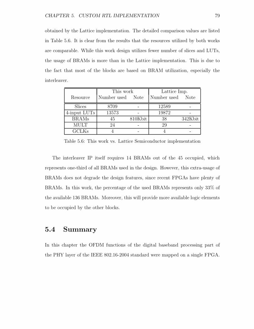
CHAPTER 5. CUSTOM RTL IMPLEMENTATION 79
obtained by the Lattice implementation. The detailed comparison values are listed
in Table 5.6. It is clear from the results that the resources utilized by both works
are comparable. While this work design utilizes fewer number of slices and LUTs,
the usage of BRAMs is more than in the Lattice implementation. This is due to
the fact that most of the blocks are based on BRAM utilization, especially the
interleaver.
This work Lattice Imp.Resource Number used Note Number used Note
Slices 8709 - 12589 -4-input LUTs 13573 - 19872 -
BRAMs 45 810Kbit 38 342KbitMULT 24 - 29 -GCLKs 4 - 4 -
Table 5.6: This work vs. Lattice Semiconductor implementation
The interleaver IP itself requires 14 BRAMs out of the 45 occupied, which
represents one-third of all BRAMs used in the design. However, this extra-usage of
BRAMs does not degrade the design features, since recent FPGAs have plenty of
BRAMs. In this work, the percentage of the used BRAMs represents only 33% of
the available 136 BRAMs. Moreover, this will provide more available logic elements
to be occupied by the other blocks.
5.4 Summary
In this chapter the OFDM functions of the digital baseband processing part of
the PHY layer of the IEEE 802.16-2004 standard were mapped on a single FPGA.
CHAPTER 5. CUSTOM RTL IMPLEMENTATION 80
The transmitter and the receiver modules were both implemented and occupied
approximately half of the available FPGA resources. The design shows a reasonable
and comparable results to other conducted studies [32] and [28]. The results reflect
clearly the reliance on the abundant BRAMs and how this work utilizes them.
Furthermore, the developed IPs in the transmitter design were firstly used in the
receiver design, and can be used in other OFDM-based designs. In the following
chapter, a higher level of abstraction approach will be presented and compared to
the custom RTL approach.

Chapter 6
AccelDSP Implementation
In the previous chapter, we highlighted the capability of RCS to accommodate
very large designs such as the PHY layer of a fixed WiMAX transceiver. How-
ever, two factors are getting more attention when it comes to hardware design.
Firstly, the need to acquaint software developers with the concept of HDL lan-
guages. The second factor is time-to-market (TTM), which is mainly based on the
design and verification time. In HDL designs, these two factors might impose a
challenge in meeting deadlines and releasing products faster. Thus, the need of
high level modeling systems is obvious, and AccelDSP is an excellent candidate in
this area. AccelDSP is a high level design tool provided by Xilinx, Inc., [38], to
enable designers to quickly code and release systems by converting their MATLAB
floating-point code into fixed-point representation. The fixed-point generated code
is then translated into HDL code and ready to be synthesized and mapped on FP-
GAs. Expected acceleration in the design time and early verification is one of the
main contributions of AccelDSP, as well as providing architecture trade-off analy-
81

CHAPTER 6. ACCELDSP IMPLEMENTATION 82
sis. The goal is to compare the AccelDSP approach to the custom RTL (VHDL)
approach in terms of area, performance, power and design time.
6.1 AccelDSP Design Flow
The AccelDSP synthesis tool is an integrated design environment that transforms
a MATLAB floating-point code into a hardware design that can be mapped on a
Xilinx FPGA. AccelDSP is based on the integration of a number of design tools
such as MATLAB, Xilinx ISE and other synthesizers and simulators from other
companies (e.g. Mentor Graphics and Synplicity).
6.1.1 AccelDSP Basics and Features
One of the main motivations behind using AccelDSP is to provide early verification
of the design as well as quick design time. Another reason is the capability to
analyze the different architecture trade-offs. The tool is capable of:
• analyzing a MATLAB floating-point design,
• generating the equivalent MATLAB fixed-point design,
• verifying the fixed-point MATLAB design through simulation,
• exploring design trade-offs of the implemented algorithm depending on the
target device,
• creating a synthesizable RTL HDL model and a test bench to ensure bit-true,
cycle-accurate design verification,

CHAPTER 6. ACCELDSP IMPLEMENTATION 83
• invoking other tools such as HDL simulators, RTL logic synthesizers, and
Xilinx ISE implementation tools,
• browsing the design hierarchy and view the M-files and the generated C++
and HDL source files,
• applying directives to customize parameters and functions implementations
to explore the different hardware, architectures
• generating Xilinx System Generator blocks.
For AccelDSP, to synthesize any MATLAB design two main files are needed,
a function file and script file. The script file contains the main function call and
a streaming loop. This streaming loop is used to pass the test bench input data
and receive the results. Other parts of the script file might contain input vectors
initialization and output verification, even though these are not synthesizable parts
of the code. The function m-file contains the actual design that need to be syn-
thesized. This function file might contain the whole design or it might call other
design functions, where parameters passed to and received from the top-level design
function represent the inputs and outputs of hardware module.
6.1.1.1 Parameters and Functions Implementation
One of the main features of AccelDSP is providing the designer with the capa-
bility to choose how a specific parameter or function is going to be implemented
in hardware. For example, a sin(x) function could be chosen to be implemented
using the CORDIC algorithm or the bipartite table, also the architecture could be

CHAPTER 6. ACCELDSP IMPLEMENTATION 84
traded-off between speed vs. area. The other method of customization is through
defining the bit-width and the quantization level. The inputs, outputs and internal
variables can be customized to a certain width and certain fixed-point quantization
representation or could be left to be inferred from the coding style. This will enable
an early trade-off analysis of the effect of floating-point to fixed-point conversion
before targeting the hardware platform.
6.1.1.2 Hardware Architecture Exploration
In addition to parameter and function customization, AccelDSP also enables the
designer to explore different hardware architectures to trade between area and per-
formance, which is based on two main techniques. The first considers any′′
For
Loops′′
implemented in the design function. A′′
For Loop′′
could be chosen in Ac-
celDSP to be fully rolled, fully unrolled or partially rolled. Fully unrolling a′′
For
Loop′′
will provide better performance by replicating the same hardware and run-
ning the application in parallel. However, this comes with the high cost of the
utilized resources. In this case, a partial rolling might work as a middle solution,
yet not all for loops are naturally rollable. In addition to for loops rolling and
unrolling, the same principle could be applied to matrices operations (+,- and *).
The other architecture exploration technique deals with mapping a variable, in
specific arrays, to memory. AccelDSP utilizes four directives: no mapping, map
to single-port RAM, map to a dual-port RAM or map to single-port ROM. These
directives affect greatly the number of clocks required to perform reading and writ-
ing operations. It is the nature of the single-port RAM that does not allow a read
and a write operations to be performed at the same clock cycle, while it could be

CHAPTER 6. ACCELDSP IMPLEMENTATION 85
performed using a dual-port RAM. However, the dual-port RAM utilizes the same
single-port RAM block to be occupied on the FPGA. Thus, in targeting FPGAs,
dual-port and single-port memories are all mapped to the same sized block RAM, so
specifying dual-port may increase performance over single-port without increasing
area. The other two options, no map and ROM mapping, are viable when a small
sized array or an array holding constant values have to be mapped. Still though,
mapping arrays to memory blocks will not enable access to all memory elements
at the same time, so at most a read and a write operations can be performed in a
single clock cycle.
6.1.2 Synthesis Flow
The synthesis flow of AccelDSP integrates the different steps required to transform
a floating-point design into hardware module, to verify the design and to finally
implement it. In AccelDSP, the synthesis flow is composed of three flows: the
ISE flow, the XSG flow and the HW-Cosim flow, where the three flows have been
utilized in this work. The ISE flow, is the default flow and it is used to create the
design and verify it at the gate-level. The flow is depicted in Figure 6.1, where it
shows the steps required and the produced files of each step. The process starts
by analyzing the floating-point model to define the variables shape. Later, the
tool generates the fixed-point model and applies any quantization directives. After
verifying the fixed-point model, the RTL model could be generated either in VHDL
or Verilog. The test bench defined in the script file is used also to build the HDL
test bench for RTL verification.
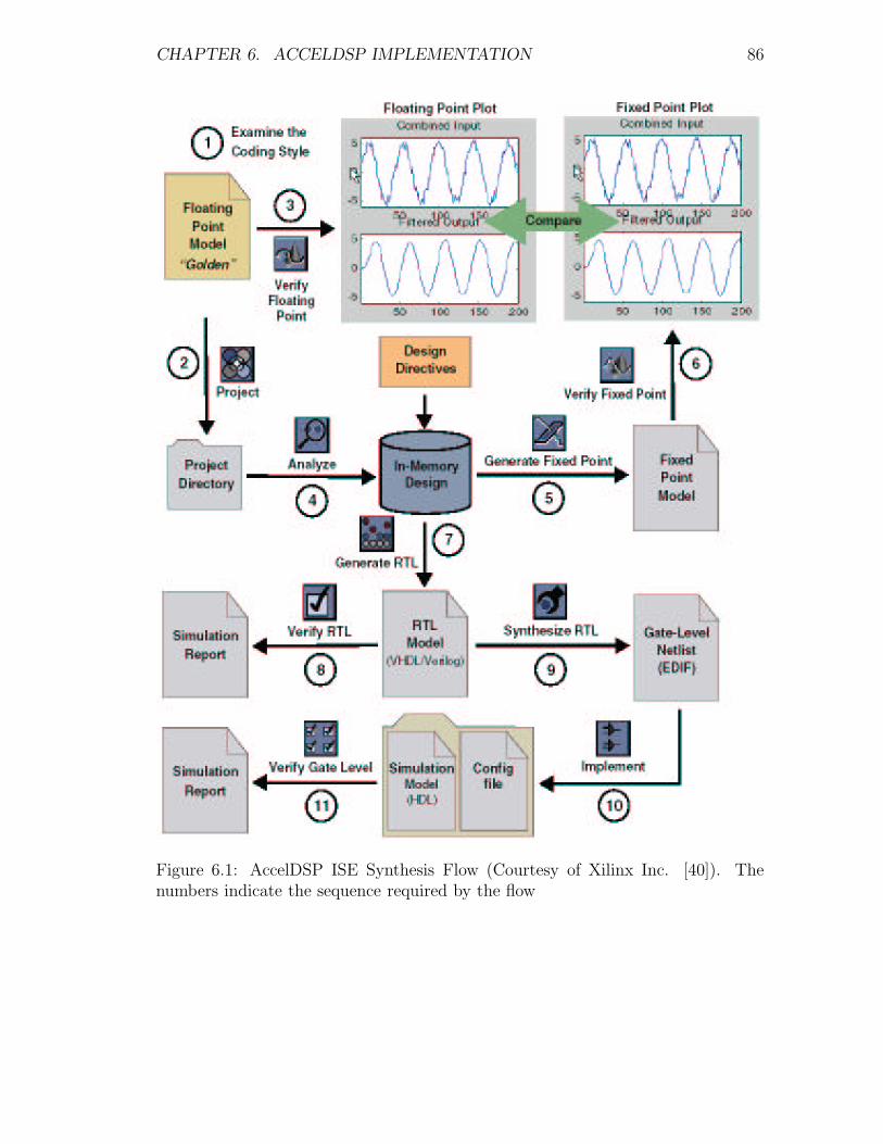
CHAPTER 6. ACCELDSP IMPLEMENTATION 86
Figure 6.1: AccelDSP ISE Synthesis Flow (Courtesy of Xilinx Inc. [40]). Thenumbers indicate the sequence required by the flow

CHAPTER 6. ACCELDSP IMPLEMENTATION 87
The other synthesis flow is used to generate XSG blocks that can be entered in
a larger design. The flow follows the same steps as the ISE flow, yet the different
steps follow the RTL generate and verify steps. After generating the RTL model
and verifying it against the fixed-point model, the RTL model is used to build the
XSG block that can be added to an existing library or to create a new Simulink
library. The final synthesis flow is the HW-Cosim flow, in which the generated RTL
is verified and simulated in hardware. This will ensure that the design will function
correctly after mapping it on the targeted FPGA. The last two flows are described
in more details in Appendix C.
6.2 Transmitter Design and Trade-offs
In this approach only the transmitting chain was implemented by applying the
same methodology described in Chapter 4. Each block was coded in MATLAB
in floating-point representation; converted to fixed-point and then the HDL files
were generated and finally synthesized and mapped. As an add-on, for each block
an XSG IP was generated, and finally a WiMAX IPs XSG library was produced.
To report a reasonable comparison, the same high level of abstraction model was
used. However, few details have been altered because of the required adaptations to
the available MATLAB built-in functions. Furthermore, few MATLAB functions
were not synthesizable. For example, the RS-encoder function accepts as input the
whole block (n bytes) to be processed, which will generate in hardware a module
with 8*n input pins. This mandates that the same input and output pins used in
the pure VHDL design are kept in the AccelDSP design.

CHAPTER 6. ACCELDSP IMPLEMENTATION 88
The main difference in the coding is based on the′′
Forloop′′
utilization in the
MATLAB code. These For loops are later traded between speed and area in the
hardware implementations, which will be explained in section 6.2.2.
6.2.1 Design Trade-offs
The architecture trade-offs explored in this work mainly concentrate on translating
the′′
For Loops′′
into hardware and the variables mapping to memory elements. In
the′′
For Loops′′
translation, two options are considered: fully unrolling and fully
rolling. Fully rolling indicates that the same hardware circuitry required to perform
the function is utilized for every iteration. Accordingly, the execution of the′′
For
Loop′′
will take (n) cycles, where n is the number of iterations. On the other hand,
a fully unrolled mechanism replicates the design, whenever it is possible, to perform
the same function in parallel in one clock cycle. However, it is expected that the
fully unrolled designs will occupy more area.
Regarding variables mapping, three options are explored: no mapping, map-
ping to single-port RAMs and mapping to double-port RAMs. The effect will be
mainly in the number of clock cycles required to perform read and write operations.
Furthermore, applying the no-mapping option will not utilize the available block
RAMs and will exhaust the available slices and LUTs. In each of the following
subsections, the main trade-offs are presented and the obtained results are listed in
Tables 6.1, 6.2, 6.3 and 6.4.
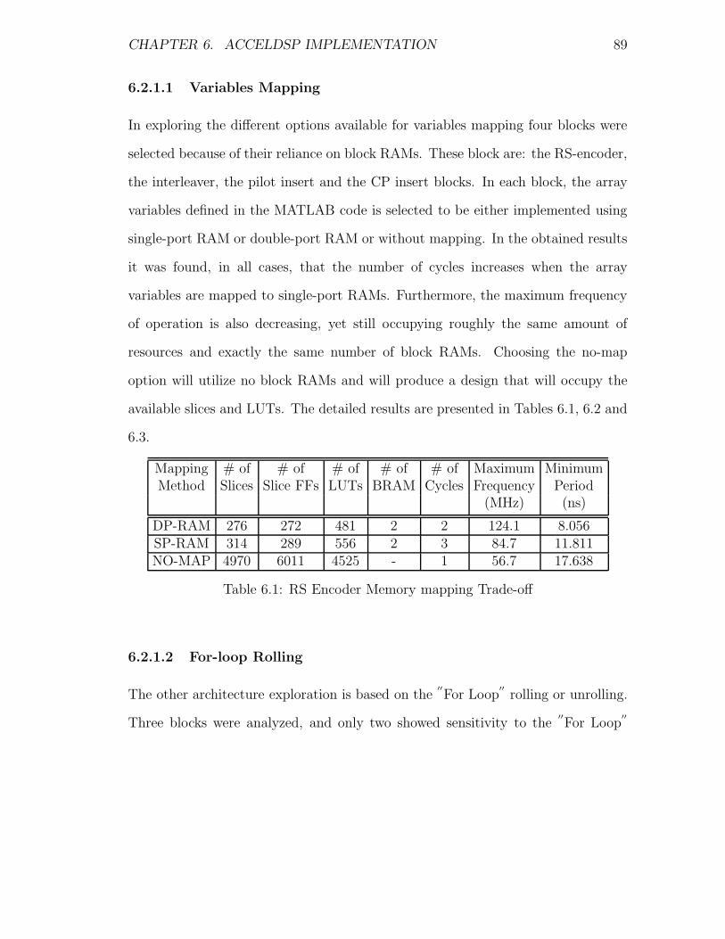
CHAPTER 6. ACCELDSP IMPLEMENTATION 89
6.2.1.1 Variables Mapping
In exploring the different options available for variables mapping four blocks were
selected because of their reliance on block RAMs. These block are: the RS-encoder,
the interleaver, the pilot insert and the CP insert blocks. In each block, the array
variables defined in the MATLAB code is selected to be either implemented using
single-port RAM or double-port RAM or without mapping. In the obtained results
it was found, in all cases, that the number of cycles increases when the array
variables are mapped to single-port RAMs. Furthermore, the maximum frequency
of operation is also decreasing, yet still occupying roughly the same amount of
resources and exactly the same number of block RAMs. Choosing the no-map
option will utilize no block RAMs and will produce a design that will occupy the
available slices and LUTs. The detailed results are presented in Tables 6.1, 6.2 and
6.3.
Mapping # of # of # of # of # of Maximum MinimumMethod Slices Slice FFs LUTs BRAM Cycles Frequency Period
(MHz) (ns)
DP-RAM 276 272 481 2 2 124.1 8.056SP-RAM 314 289 556 2 3 84.7 11.811NO-MAP 4970 6011 4525 - 1 56.7 17.638
Table 6.1: RS Encoder Memory mapping Trade-off
6.2.1.2 For-loop Rolling
The other architecture exploration is based on the′′
For Loop′′
rolling or unrolling.
Three blocks were analyzed, and only two showed sensitivity to the′′
For Loop′′

CHAPTER 6. ACCELDSP IMPLEMENTATION 90
Mapping # of # of # of # of # of Maximum MinimumMethod Slices Slice FFs LUTs BRAM Cycles Frequency Period
(MHz) (ns)
DP-RAM 139 95 242 2 1 73.4 13.621SP-RAM 98 79 167 2 4 99.1 10.092NO-MAP 13700 16443 9194 - 1 110.9 9.02
Table 6.2: Pilot Insert Memory mapping Trade-off
Mapping # of # of # of # of # of Maximum MinimumMethod Slices Slice FFs LUTs BRAM Cycles Frequency Period
(MHz) (ns)
DP-RAM 182 115 311 4 1 138.9 7.2SP-RAM 133 117 226 4 4 98.1 10.189NO-MAP 27366 32836 18209 - 1 108.3 9.231
Table 6.3: CP Insert Memory mapping Trade-off
trade-off. The first block, the randomizer, showed no effect, which is due to the
sequential nature of the block. The other two blocks, the CC-encoder and the
interleaver, showed a significant trade-off in area vs performance when comparing
the two architecture. In the CC-encoder case, the unrolled architecture was not
synthesizable due to the existence of the puncturing procedure inside the′′
For
Loop′′
iterations. In the other case, the interleaver design showed also an increase
in the number of resources required when the′′
For Loop′′
is fully unrolled. The
increase represents approximately 4-6 times the number of resources required in the
rolled design. The results are shown in Table 6.4.

CHAPTER 6. ACCELDSP IMPLEMENTATION 91
For-Loop # of # of # of # of # of Maximum MinimumTrade-off Slices Slice FFs LUTs BRAM Cycles Frequency Period
(MHz) (ns)
Rolled 145 127 257 3 13 185.8 6.31Unrolled 8469 556 14072 17 1 36.5 27.42
Table 6.4: Interleaver Rolling-unrolling Trade-off
6.3 Results
In this section, the results obtained after mapping the transmitter design using
AccelDSP are reported. These results also show the difference, in terms of the
number of resources and performance, between the AccelDSP and the custom RTL
(VHDL) approaches. Table 6.5 summarizes the resources required by the complete
transmitter design. Table 6.6 lists the different IPs utilization resources. The
obtained results shows that a fixed WiMAX PHY layer transmitter design could
be implemented on a medium-size FPGA with an occupation rate of about 35% of
the available resources when mapped on the Xilinx Virtex-II Pro chip.
Resource Available TxResources used %
Slices 13696 5982 43Slice FFs 27392 6485 23
4-input LUTs 27392 7856 28Bonded IOBs 556 53 13
BRAMs 136 40 29MULT 136 12 8GCLKs 16 1 6
Table 6.5: AccelDSP Transmitter Resource Utilization
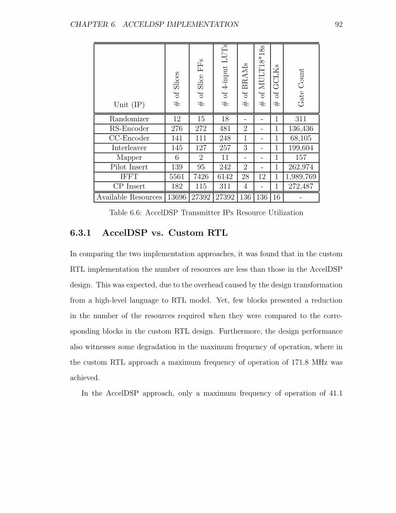
CHAPTER 6. ACCELDSP IMPLEMENTATION 92
Unit (IP) #of
Slice
s
#of
Slice
FFs
#of
4-in
put
LU
Ts
#of
BR
AM
s
#of
MU
LT
18*1
8s
#of
GC
LK
s
Gat
eC
ount
Randomizer 12 15 18 - - 1 311RS-Encoder 276 272 481 2 - 1 136,436CC-Encoder 141 111 248 1 - 1 68,105Interleaver 145 127 257 3 - 1 199,604Mapper 6 2 11 - - 1 157
Pilot Insert 139 95 242 2 - 1 262,974IFFT 5561 7426 6142 28 12 1 1,989,769
CP Insert 182 115 311 4 - 1 272,487
Available Resources 13696 27392 27392 136 136 16 -
Table 6.6: AccelDSP Transmitter IPs Resource Utilization
6.3.1 AccelDSP vs. Custom RTL
In comparing the two implementation approaches, it was found that in the custom
RTL implementation the number of resources are less than those in the AccelDSP
design. This was expected, due to the overhead caused by the design transformation
from a high-level language to RTL model. Yet, few blocks presented a reduction
in the number of the resources required when they were compared to the corre-
sponding blocks in the custom RTL design. Furthermore, the design performance
also witnesses some degradation in the maximum frequency of operation, where in
the custom RTL approach a maximum frequency of operation of 171.8 MHz was
achieved.
In the AccelDSP approach, only a maximum frequency of operation of 41.1
CHAPTER 6. ACCELDSP IMPLEMENTATION 93
MHz was obtained, yet this still conforms to the standard requirement of 14 MHz
frequency of operation. This significant difference can be attributed to the lack of
multiple clock domains in AccelDSP which results in certain blocks being idle for
a considerable time waiting for the slow blocks to finish processing.
The other comparison figure is the power consumption, based on the Xilinx
Web Power tool. The estimation was based on the number of resources used, the
activity rate and the main clock, which was set to the values close to the maximum
frequency of operation. In this case the AccelDSP design indicated less power
consumption, which was decreased by a factor of 1/4. However, due to the longer
time required to produce a symbol in the AccelDSP approach, the total energy
consumed is eventually higher.
In the AccelDSP implementation only one GCLK was used in the design, while
in the pure VHDL design 4 GCKLs were used to match the processing rate of each
block. This concludes that the AccelDSP tool should be used in designing DSP
blocks in larger systems design, but not a first option in designing complex systems.
However, a remarkable advantage of using AccelDSP was the fast and early-phases
trade-off analysis conducted, as well as the fast design time. By counting the
number of working days required to complete both designs, it was estimated that
the AccelDSP design required about 30 working days. On the other hand, the
custom RTL (VHDL) design spanned over a period of 50-60 days, yet not taking
into account that certain IPs have been imported from a previous conducted work
[2]. The detailed comparison results are listed in Table 6.7.
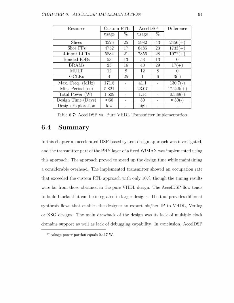
CHAPTER 6. ACCELDSP IMPLEMENTATION 94
Resource Custom RTL AccelDSP Differenceusage % usage %
Slices 3526 25 5982 43 2456(+)Slice FFs 4752 17 6485 23 1733(+)
4-input LUTs 5884 21 7856 28 1972(+)Bonded IOBs 53 13 53 13 0
BRAMs 23 16 40 29 17(+)MULT 12 8 12 8 0GCLKs 4 25 1 6 3(-)
Max. Freq. (MHz) 171.8 - 41.1 - 130.7(-)Min. Period (ns) 5.821 - 23.07 - 17.249(+)Total Power (W)1 1.529 - 1.14 - 0.389(-)
Design Time (Days) ≈60 - 30 - ≈30(-)Design Exploration low - high - -
Table 6.7: AccelDSP vs. Pure VHDL Transmitter Implementation
6.4 Summary
In this chapter an accelerated DSP-based system design approach was investigated,
and the transmitter part of the PHY layer of a fixed WiMAX was implemented using
this approach. The approach proved to speed up the design time while maintaining
a considerable overhead. The implemented transmitter showed an occupation rate
that exceeded the custom RTL approach with only 10%, though the timing results
were far from those obtained in the pure VHDL design. The AccelDSP flow tends
to build blocks that can be integrated in larger designs. The tool provides different
synthesis flows that enables the designer to export his/her IP to VHDL, Verilog
or XSG designs. The main drawback of the design was its lack of multiple clock
domains support as well as lack of debugging capability. In conclusion, AccelDSP
1Leakage power portion equals 0.417 W.

CHAPTER 6. ACCELDSP IMPLEMENTATION 95
is a tool that enables faster design time and early design trade-offs analysis.

Chapter 7
Configurable Processors
Implementation
In the previous two chapters, the capability of implementing the OFDM func-
tions of the fixed WiMAX PHY layer on an FPGA was investigated and presented.
However, other approaches are also worth pursuing, and among them Application
Specific Instruction-set Processors (ASIP) or as we will refer to them in this chapter
by configurable processors. Since ASIPs have close characteristics to reconfigurable
platforms we are investigating them in this dissertation. Among those characteris-
tics are the relatively fast design time, rapid prototyping on FPGA platforms and
the promise of architectural exploration. The configurable processors targeted in
this work are the Tensilica Xtensa family of processors [13]. The Xtensa processors
are configurable cores that can be initialized and defined at the micro-architectural
level, as well as being extensible at the instruction set level through customization.
This chapter is organized as following: the Tensilica Xtensa processor main
96

CHAPTER 7. CONFIGURABLE PROCESSORS IMPLEMENTATION 97
features and design flow are addressed in section 7.1. In section 7.2, the scope of
this approach is defined while highlighting the importance of the conducted work.
Furthermore, this section also explains the design details and the main steps, while
sections 7.3 and 7.4 lists the results obtained (performance, area and power) and
compares them to the previous approaches.
7.1 Tensilica Configurable Processors
Traditional general-purpose processors, e.g. RISC processors, are of use in many
applications, but they may not be powerful enough for building complex System-
on-Chip (SOC) designs. Even though one might argue that using a number of these
processors might work for complicated applications, yet they are unable to run fast
enough to match the sophisticated tasks in today’s embedded SOCs. Furthermore,
the requirements for power consumption, area and performance are rising as the
algorithms are becoming more complicated. ASIPs are seen as a middle ground
between general purpose processors and ASICs, where customization on the in-
struction set and data path levels feeds both the application specific demands and
the easiness of design.
7.1.1 Xtensa Processors
Tensilica Inc. led the way in designing Application Specific Instruction set Pro-
cessors through its Xtensa configurable extensible processors. The processors are
configurable through the Tensilica processor configuration-generation design flow
known as Xtensa Processor Generator (XPG), which allows the designers to define

CHAPTER 7. CONFIGURABLE PROCESSORS IMPLEMENTATION 98
the processor micro-architectural blocks. This configurability permits the sizing of
the processor to meet the targeted application demands. Designers use the Xtensa
Xplorer Integrated Development Environment (IDE) to evaluate the effects of var-
ious configuration changes and new instructions on power, area and performance.
Extensibility in the Tensilica Xtensa processors is accomplished through defining
the main hot spots in the developer C/C++ code and rewriting them in the Ten-
silica Instruction Extension (TIE) language, a Verilog-based language. The benefit
of the TIE language is that it defines new instructions, registers and register files
of any size, as well as defining new in-out ports. The TIE extensions are compiled
using the TIE Compiler, which generates the necessary files needed to customize
the software tool chain and extend the instruction-set simulator. In addition, it
provides a valuable estimation on the additional gates generated.
Other means of using the Tensilica approach for SOC design is through running
the XPRES (Xtensa Processor Extension Synthesis) Compiler, which automatically
generates one or more TIE files to improve the performance of the application,
while providing trade-off between the performance achieved versus the additional
area utilized. The resulting generated TIE files could be refined or extended further
through writing other TIE extensions. The XPRES Compiler performs exploration
of the different configurations in a reasonable amount of time, relative to the algo-
rithm sophistication. The rapid exploration allows the designer to trade between a
variety of both the automatically and manually generated TIE instructions.
CHAPTER 7. CONFIGURABLE PROCESSORS IMPLEMENTATION 99
7.1.2 Design Flow
Tensilica provides an integrated environment that allows the developer to perform
the different tasks of the design flow. Designing in the Tensilica Xplorer IDE
starts by writing the C/C++ code for the desired application. The next step is
generating the processor through the processor generator interface. In this step, the
developer specifies the instruction-set options, memory, peripherals and interfaces.
The tool provides means to explore different configurations to obtain the optimal
architecture.
Following the generation of the desired processor, the written code could be pro-
filed against the generated processor to define the main bottlenecks in the C/C++
code. The approach then is to extend the processor ISA through the TIE language.
The written TIE code is compiled and the required libraries are generated and em-
bedded automatically to provide support inside the IDE environment. The added
TIE instructions could then be easily added inside the C code, and profiling again
will reveal the speed-up achieved against using the pure processor ISA. Figure 7.1
depicts the different steps involved in the design flow.
7.2 Design Details
The main objective for this part of the dissertation is to provide the interested
SOC/FPGA designer with an insight on the capability of ASIPs to implement
efficient wireless communication modules with some design trade-offs. The scope
of this approach is only limited to the coding part, which includes: randomization,

CHAPTER 7. CONFIGURABLE PROCESSORS IMPLEMENTATION 100
Figure 7.1: Xtensa Design Flow
FEC and interleaving. The results obtained are then compared to the same blocks
implemented by the custom RTL and AccelDSP approaches.
The ASIP approach relies on developing the complete C code for the coding
functions. The developed code is then tested and profiled to define the main bot-
tlenecks in the design. In this approach, the same design and verification method-
ology applied in the previous approaches was followed. First, each function was
designed, tested and profiled separately to define the main hot spot(s). The devel-
oped functions were then integrated and profiled again to confirm on those defined
hot spot(s). Utilizing the available tools from Tensilica, the XPRES compiler, it
was also possible to generate a number of TIE configurations and later target the
defined configurable processor for further instruction set extension. The provided
TIE language was finally used to convert the software bottlenecks into specific in-
structions that can allow the design to execute faster through parallelization and
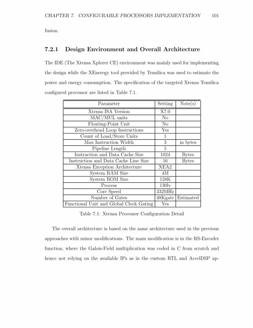
CHAPTER 7. CONFIGURABLE PROCESSORS IMPLEMENTATION 101
fusion.
7.2.1 Design Environment and Overall Architecture
The IDE (The Xtensa Xplorer CE) environment was mainly used for implementing
the design while the XEneregy tool provided by Tensilica was used to estimate the
power and energy consumption. The specification of the targeted Xtensa Tensilica
configured processor are listed in Table 7.1.
Parameter Setting Note(s)
Xtensa ISA Version X7.0MAC/MUL units No
Floating-Point Unit NoZero-overhead Loop Instructions Yes
Count of Load/Store Units 1Max Instruction Width 3 in bytes
Pipeline Length 5Instruction and Data Cache Size 1024 Bytes
Instruction and Data Cache Line Size 16 BytesXtensa Exception Architecture XEA2
System RAM Size 4MSystem ROM Size 128K
Process 130lvCore Speed 332MHz
Number of Gates 48Kgate EstimatedFunctional Unit and Global Clock Gating Yes
Table 7.1: Xtensa Processor Configuration Detail
The overall architecture is based on the same architecture used in the previous
approaches with minor modifications. The main modification is in the RS-Encoder
function, where the Galois-Field multiplication was coded in C from scratch and
hence not relying on the available IPs as in the custom RTL and AccelDSP ap-
CHAPTER 7. CONFIGURABLE PROCESSORS IMPLEMENTATION 102
proaches. The signals passed between the blocks were also kept the same, as well
as the input and output ports for the whole design. This step was needed to verify
the comparison results at the end of this chapter.
The different blocks of the coding part were implemented in separate functions
with additional sub-functions written to support each block. The main functions of
the overall design are: randomizer function, rs-ip function, cc-ip function and the
interleaving function (refer to Section 5.1 for the functions’ details). Among these
functions, the rs-ip function required three additional sub-functions: the GFMult
that is responsible on performing Galois-Field multiplications and the post-rs and
tailing sub-functions that are responsible on providing shortened code support. In
the cc-ip function, the only additional sub-function is the puncturing operation,
that enables different punctured coding rates of 2/3, 3/4 and 5/6.
7.2.2 Profiling Results
In this section we will study the obtained profiling results that will be used to
rewrite the C code based on the TIE language as demonstrated by Table 7.2. The
table lists the main functions and sub-functions, while disregarding minor and less
critical functions. The results in this table compare the profiling results obtained
for designs with/without TIE instructions extensions. It is worth mentioning that
the results are obtained with no compiler directives, and the specification of the
targeted configurable processor are those mentioned in Table 7.1.
It is clear from Table 7.2 that the main hot spot of the design is centered
around the Galois-Field multiplication (GFMult) used in the RS-Encoder (rs-ip)

CHAPTER 7. CONFIGURABLE PROCESSORS IMPLEMENTATION 103
Pure C Code TIE-Extended CodeFunction Function Total Function Total Speed-Up
Name Cycles Cycles (%) Cycles Cycles (%) (Ratio)
GFMult 340468 28.90 3120 0.8 109.1RS-ip 318743 27.07 28193 7.17 11.3cc-ip 93128 7.91 67914 17.28 1.37main 83495 7.09 68678 17.47 1.2
memset 74910 6.36 62040 15.78 1.2memcpy 68856 5.84 53196 13.53 1.3
puncturer 60624 5.15 31093 7.91 1.95randmoizer 55030 4.67 6240 1.59 8.82
post-rs 38012 3.22 38012 9.67 1tailing 32787 2.79 32787 8.36 1
All 1177109 100 392969 100 2.995
Table 7.2: Profiling Results (Pure C Code vs TIE-extended Code)
function. Other functions worth further customization are the puncturing function
and the array shifting operation in both the randomization and CC-Encoder (cc-
ip) functions. The only block that did not require any further customization is
the interleaving block (not listed here), which was built from many read-write
operations that were inherently sequential.
The ISA extensions through the TIE instructions show clearly the gain in speed-
up, where as demonstrated by Table 7.2, the GFMult function had a 109x speed-
up. This corresponds to a reduction in the parent function, rs-ip, of 11.3 times,
since other sub-functions such as post-rs and tailing are still executing in the same
number of cycles. The other remarkable decrease in the number of cycles required
is represented by the randomizer function, where it was reduced with a factor of
8.82. However, the randomizer function does not represent a heavy weight of the
overall design, since it represents only 4.67% of the total number of cycles required

CHAPTER 7. CONFIGURABLE PROCESSORS IMPLEMENTATION 104
by the pure C code implementation.
On average, the speed-up gained with the TIE-extensions in place represents a
reduction in the total number of cycles of 66% or a 3x speed-up. An important
factor that is worth addressing is the additional number of gates generated. Based
on the TIE compiler an additional 23,097 gates need to be generated to employ the
added instructions, which represents a 50% addition to the original core area.
Hence, further optimization was required to reduce the area generated while
maintaining a reasonable amount of speed-up. In addition, optimizations utilizing
the compiler directives were also used to obtain further improvements. At the
compiler level, three directives were applied to enhance the speed. These directives
were: an optimization level of 3 for speed, enabling the interprocedural optimization
and enabling the automatic vectorization option. Enabling these three directives
and running the profiling process provided results that reduced the total number of
cycles required by a factor of 3.67 to 5.14. Detailed results can be found in Table
7.3.
Pure C Code TIE-Extended CodeFunction Function Total Function Total Speed-Up
Name Cycles Cycles (%) Cycles Cycles (%) (Ratio)
GFMult 80258 25.04 780 1.02 102.9RS-ip 165669 51.68 6662 8.72 24.87cc-ip 58107 18.12 30950 40.52 1.88main 62019 19.34 33316 43.62 1.86
memcpy 24656 7.69 2036 2.66 12.11All 320521 100 76372 100 4.2
Table 7.3: Profiling Results (with compiler directives enabled)
Optimization in the written TIE code did not improve the speed-up results.
CHAPTER 7. CONFIGURABLE PROCESSORS IMPLEMENTATION 105
However, it provided a decrease in the additional gates generated. The unoptimized
TIE code was estimated to occupy 23,097 gates, while the optimized TIE code
required only 14,931 gates. This represents a decrease of 35.36% in the gate count
from the unoptimized TIE code, and represents an additional gate count of only
31.1% of the original processor’s gate count.
7.3 Results
The design was tested and simulated in the Xtensa Xplorer CE version 2.0.0, and
the results obtained indicated the conformance of the tested IPs to the IEEE 802.16-
2004 standard document. The design was ported on the Xtensa 7 processor tar-
geting a 130nm lv process, with a configuration equivalent to a total gate count
estimated to be approximately equal to 48Kgates (an area of 0.39 mm2), and run-
ning at a maximum frequency of 330 MHz.
7.3.1 Performance and Area
From the profiling results listed in Tables 7.2 and 7.3 it is clear that a speed-
up of approximately 3x-4x is achievable with the added TIE extensions, which
contributed to only 31% increase in the original core area. The main contribution
of this speed-up, as well as area increase, comes from the GFMult function that
was accelerated by a factor of 109x and increased the gate count by 6346 gates,
about 42.5% of the total gate count of the added TIE instructions.

CHAPTER 7. CONFIGURABLE PROCESSORS IMPLEMENTATION 106
7.3.2 Power
Power consumption was yet another important parameter to be investigated. The
XEnergy tool by Tensilica was used to run both the pure C code and the TIE-
extended code against the configured core with the TIE extensions. The results are
listed in Table 7.4 with a little modification of the generated processor to account
for mapping the design on a Xilinx Virtex-II FPGA and running at the lowest
possible frequency of 150 MHz.
The results obtained show that the total power consumed by the code with TIE
support increases by 0.3103 mW. However, this does not represent the total energy
consumed, since the number of cycles are reduced by a factor of 5. The total energy
in the code with the TIE support is found to be 4.68 times less. Thus, this energy
saving, in addition to the speed-up gained, can be tolerated for the additional gates
generated.
Power (mW) Energy (µJ)Code Cycles Dynamic Leakage Total Dynamic Leakage Total
Pure C 503359 21.7001 1.0295 22.7296 72.8559 3.4564 76.3123TIE 104488 22.0104 1.3767 23.3872 15.3398 0.9595 16.2993
Table 7.4: Power/Energy Results (Pure C Code vs TIE-extended Code)
7.4 Overall Comparison
Designing the same algorithm/standard with different flows/technologies requires
these approaches to be compared and results revealed for interested designers. In
this section, a summary of the results obtained by the three different approaches

CHAPTER 7. CONFIGURABLE PROCESSORS IMPLEMENTATION 107
will be compared in terms of performance, area, power and design time. It is worth
mentioning that the underlying technology for the Tensilica approach is targeting
ASIC designs which explains the highest frequency of operation value of 330 MHz.
First, since the platforms differ in the three applied approaches, comparing the
performance based on the value of the maximum frequency of operation might be
misleading. Thus, the term throughput is used to compare the three approaches,
which refers to the number of OFDM symbols processed in a unit of time, or the
time required to process one OFDM symbol.
To perform the comparison, the three approaches were set to the maximum fre-
quency of operation, and the time for processing one OFDM symbols was recorded.
It was found that for the Tensilica Xtensa processor a time of 314 µsec was required
to perform the coding for one OFDM symbol, while the AccelDSP and custom RTL
approaches required approximately half and third of that time respectively. Table
7.5 lists the detailed results.
Regarding the occupied area, the equivalent number of gates is used as the basis
for the comparison, which is the equivalent of a 2-input NAND gate. It is expected
that the configurable processor option will be the design with the less number
of gates required, and that is confirmed by the 62,931 gates. On the other hand,
both the AccelDSP and pure VHDL approaches required 404,456 and gates 733,112
respectively. This significant increase in the number of gates could be contributed
to the highest degree of parallelism in the FPGA designs, while the ASIP design
was kept at a lower level of parallelism by introducing TIE extensions only to the
major hot spots in the design.

CHAPTER 7. CONFIGURABLE PROCESSORS IMPLEMENTATION 108
The other significant factor is the power consumption, which should favor the
configurable processor approach since FPGAs are well known for the high leakage
power consumptions due to the extra embedded logic. For this round of comparison,
again the highest frequency of operation was targeted to obtain the power consumed
at this specific frequency.
For the Tensilica Xtensa processor operating at a maximum frequency of 330
MHz, the power consumption was calculated to be 50.31 mW to process one OFDM
symbol. In the two FPGA approaches, the total power needed to process one
OFDM symbol was estimated to be in the order of 10 and 15 times that of the
Xtensa processor. This increase was expected, even though the noticeable increase
is mainly due to the leakage power. The leakage power in the FPGA designs were
found to be in the order of 417 mW, while in the Xtensa processor it was only 1.37
mW. It is worth mentioning that the underlying technology for both platforms was
set at 130 nm.
ApproachFactor Custom RTL AccelDSP Tensilica ASIP
Max. Freq. of Operation (MHz) 100 40 330Throughput (µsec/symbol) 85 177 314
Area Occupied (Gates) 404,456 733,112 62,931Total Power (mW) 780 588 50.31Design Time (Days) 60 30 30
Table 7.5: The Three Approaches Trading Table
The final factor to consider is the design time, which was approximately equal for
both the Tensilica and AccelDSP approaches 1. An important factor to remember
1A period of approximately one month was all that was required to write the code and test it.
CHAPTER 7. CONFIGURABLE PROCESSORS IMPLEMENTATION 109
is that the Tensilica approach was based on the output C code from the AccelDSP
tool, which saved time by modifying and optimizing the available code rather than
writing it from scratch.
7.5 Summary
In this chapter, the approach of utilizing ASIP design flow using the Tensilica
tools was investigated, and the coding part of the fixed WiMAX PHY layer was
implemented. The approach validated the hypothesis about the fast design time,
the design-time architectural exploration capability and the feasible technology
behind ASIP in general and Tensilica Xtensa processors in particular. The tools
provided by Tensilica allow for easy development and early verification results. In
addition, the powerful TIE language proved to provide a mean for speed-up gains
in the most computationally intensive algorithms, with the least hardware overhead
and a very significant energy savings results.

Chapter 8
Conclusion
Wireless communication standards in general, and WiMAX in particular, are
gaining a significant share in the broadband access service market. These standards
are still in the early stages of development, and in-field programmability as well
as fast prototyping are essential for their development and deployment. Reconfig-
urable computing is a promising paradigm for implementing these standards, espe-
cially with the increased capacity and capability of these platforms. Furthermore,
different design CAD tools and implementation approaches exist. This dissertation
attempts to explore and exploit the capability of reconfigurable computing systems,
and FPGAs in specific, to accommodate these standards, as well as providing any
interested reader with the basic figure of merit to guide them in the selection be-
tween the available implementation approaches. Thus, two approaches targeting
implementing all OFDM functions of the digital baseband processor of the PHY
layer in the fixed-WiMAX standard on FPGA were studied, and an ASIP design
approach was also investigated.
110

CHAPTER 8. CONCLUSION 111
The first part of the thesis highlighted the capability of FPGAs to accommodate
the targeted standard functions in both the transmitter and receiver chains. The
main focus was to develop a library of custom RTL synthesizable IP cores that could
be utilized by WiMAX and other OFDM-based standards. The results obtained in
this dissertation indicate that only about 50% of the resources available in a medium
sized FPGA are necessary to map the transmitter and receiver chains. The results
also provided an insight on the area required by each IP in addition to the timing
results. Comparing the obtained results also shows close figures to an industrial
work by Lattice Semiconductor [28]. Furthermore, this thesis showed improvement
in the resources utilized when compared to a previous academic conducted work
[32], in which only the modulation part of the transmitter chain was implemented.
The second phase of this thesis targeted another design flow that utilizes a high
level modeling system - the AccelDSP tool. In this approach only the transmit-
ter chain was mapped on the same FPGA, and the results obtained showed less
efficiency in terms of area and performance. However, the approach presented an
interesting design method that is characterized by the fast design time which was
cut to half the time required by the custom RTL approach. In addition, the ap-
proach provided an easy and fast design exploration environment, that allowed five
different trade-offs to be performed at the early design stages. The outcome of this
approach was a list of comparison figures and a library of Simulink blocks for the
targeted OFDM functions.
Finally, the third phase targeted the Tensilica Xtensa configurable processor
while limiting the design only to the coding functions in the transmitter chain. The

CHAPTER 8. CONCLUSION 112
approach was based on defining application specific instructions which resulted in a
speedup of 3x-4x over the pure software implementation. The instruction extension
technique also presented energy saving, where the energy consumption was reduced
by a factor of 4.68. In comparing this approach to the two earlier design flows,
this approach showed an equivalent figure for the design time required compared
to the AccelDSP approach. Furthermore, the approach also showed a considerable
power saving equivalent to 1/10 and 1/15 of that estimated in the AccelDSP and
custom RTL approaches, respectively. However, the performance factor was the
only limitation and that can be attributed to the low level of parallelism exploited.
8.1 Future Work
The work presented in this thesis paves the way for a list of future work that was
limited by the implementation time required. From the implementation approaches
point of view, other approaches such as the Xilinx System Generator or the Celoxica
Handel-C could be targeted and compared to the current approaches; especially the
AccelDSP approach. Furthermore, the designed IPs could still further be optimized,
and a mixture of IPs from the two libraries generated could be used to implement
a more efficient system.
From the OFDM point of view, extending the chain to include the baseband
to broadband conversion functions such as pulse shaping and digital up-down con-
version is really desirable. The design should enable a more realistic testing of the
system against other factors such as Error Vector Magnitude (EVM), Bit-Error
Rate (BER) and Signal-to-Noise Ratio (SNR). A recent publication by Boumaiza,

CHAPTER 8. CONCLUSION 113
[41], shows a preliminary work conducted that utilizes the proposed idea.
Finally, other avenues related to interesting OFDM issues that are worth pursu-
ing include the implementation of MIMO-OFDM systems, optional coding blocks
and synchronization circuits. In addition, problems associated with OFDM such
as Peak-to Average Power Ratio (PAPR), which puts more burden on the power
amplifier designers is yet another area worth further investigation.
Bibliography
[1] A. Ghosh J. Andrews and R. Muhamed, Fundamentals of WiMAX: Under-
standing Broadband wireless Networking, Pearson Education, Inc., 2007.
[2] A. Sghaier S. Areibi and B. Dony, “A Pipelined Implementation of OFDM
Transmission on Reconfigurable Platforms”, in Canadian Conference on Elec-
trical and Computer Engineering. CCECE08. Niagara Falls, Canada, pp. 801–
804, May 2008.
[3] A. Sghaier S. Areibi and B. Dony, “IEEE802.16-2004 OFDM Functions Im-
plementation on FPGAs with Design Exploration”, Accepted at the FPL08
Conference, Hiedelberg, Germany, Sep., 2008.
[4] IEEE, IEEE Standard for Local and metropolitan area netwroks, Part16: Air
Interface for Fixed Broadband Wireless Access Systems, 2004.
[5] IEEE, IEEE Standard for Local and metropolitan area netwroks, Part16: Air
Interface for Fixed and Mobile Broadband Wireless Access Systems, 2006.
[6] WiMAX Forum, “http://www.wimaxforum.org”.
[7] ETSI, “www.etsi.org/WebSite/Technologies/HiperMAN.aspx”.
114

BIBLIOGRAPHY 115
[8] WiBro, “http://www.wibro.or.kr/”.
[9] Qualcomm, “http://www.qualcomm.com/qft/”.
[10] H. Schulze and C. Lueders, Theory and Applications of OFDM and CDMA:
Wideband Wireless Communications, Wiley, 2005.
[11] C. Maxfield, The Design Warrior’s Guide to FPGAs, Elsevier, 2004.
[12] M. Gohkale and P. Graham, Reconfigurable Computing: Accelerating Compu-
tation with Field-Programmable Gate Arrays, Springer, 2005.
[13] Tensilica, “http://www.tensilica.com”.
[14] L. Qian Y. Tang and Y. Wang, “Optimized Software Implementation of a
Full-Rate IEEE 802.11a Compliant Digital Baseband Transmitter on a Dig-
ital Signal Processor”, IEEE Global Telecommunications Conference, vol. 4,
pp. 2194–2198, Nov. 2005.
[15] H. Ye et al. D. Iancu, “Software Implementation of WiMAX on the Sand-
bridge SandBlaster Platform”, Lecture Notes in Computer Science, SAMOS,
vol. 4017, pp. 435–446, July 2006.
[16] F. W. Hoeksema R. Schiphorst and C. H. Slump, “A Real-Time GPP
Software-Defined Radio Testbed for the Physical Layer of Wireless Standards”,
EURASIP Journal on Applied Signal Processing, vol. 16, pp. 2664–2672, 2005.
[17] D. W. Lin Y. Chen and C. Wu, “DSP Software Implementation and Integration
of IEEE 802.16 TDD-OFDMA-Mode Downlink Transceiver Functions”, in

BIBLIOGRAPHY 116
2005 International Symposium on Communications, ISCOM2005, Kaohsiung,
Taiwan, pp. 124–127, Nov. 2005.
[18] V. Derudder et al. W. Eberle, “80-Mb/s QPSK and 72-Mb/s 64-QAM Flex-
ible and Scalable Digital OFDM Transceiver ASICs for Wireless Local Area
Netwroks in the 5-GHz Band”, IEEE Journal of Solid-State Circuits, vol. 36,
pp. 1829–1838, Nov. 2001.
[19] J. Tian H. Jiang, H. Luo and W. Song, “Design of an Efficient FFT Processor
for OFDM Systems”, IEEE Trans. on Consumer Electronics, vol. 51, pp. 1099–
1103, Nov. 2005.
[20] M. H. Sunwoo B. S. Son, B. G. Jo and Y. S. Kim, “A High-speed FFT
Processor for OFDM Systems”, IEEE Int. Sym. on Circuits and Systems,
vol. 3, pp. III–281–III–284, 2002.
[21] J. H. Moon et al. J. H. Lee, “Implementation of Application-Specific DSP for
OFDM Systems”, Proc. of the 2004 International Symposium on Circuits and
Systems, ISCAS ’04., vol. 3, pp. 665–668, May 2004.
[22] S. Areibi, “WiMAX ASIC Implementation Presentation to PolarSat”, 2005.
[23] C. Fisher et al. C. Ebeling, “Implementing an OFDM Receiver on the RaPiD
Reconfigurable Architecture”, IEEE Transactions on Computers, vol. 53,
pp. 1436–1448, Nov. 2004.
[24] K. Chang and G. Sobelman, “FPGA-based Design of a Pulsed-OFDM Sys-
tem”, in IEEE Asia Pacific Conference on Circuits and Systems. APCCAS
2006. Singapore,, pp. 1128–1131, Dec. 2006.
BIBLIOGRAPHY 117
[25] K. Masselos and N. S. Voros, “Implementation of Wireless Communcations
Systems on FPGA-based Platforms”, EURASIP Journal on Embedded Sys-
tems, vol. 7, 2007.
[26] C. Dick and F. Harris, “FPGA Implementation of an OFDM PHY”, Confer-
ence Record of the Thirty-Seventh Asilomar Conference on Signals, Systems
and Computers., vol. 1, pp. 905–909, Nov. 2003.
[27] Y. O. Park H. S. Park and C. Kim, “A Design and Performance Analysis of
OFDMA Modulator based on IEEE 802.16a Standard”, Conference Record of
the Thirty-Eighth Asilomar Conference on Signals, Systems and Computers.,
vol. 1, pp. 536–539, Nov. 2004.
[28] Lattice, “Implementation of an OFDM Wireless Transceiver using IP Cores
on an FPGA”, Technical report, Lattice Semiconductor Corporation, 2005.
[29] Altera, “Accelerating WiMAX System Design with FPGAs”, Technical report,
Altera Corporation, 2004.
[30] H. Jung J. S. Park and V. K. Prasanna, “Efficient FPGA-based Implementa-
tion of the MIMO-OFDM Physical Layer”, in Proceedings of the International
Conference on Engineering of Reconfigurable Systems and Algorithms, ERSA,
Las Vegas, Nevada, USA,, pp. 153–163, June 2006.
[31] F. Manavi and Y. R. Shayan, “Implementation of OFDM modem for the
physical layer of IEEE 802.11a Standard based on Xilinx Virtex-II FPGA”,
IEEE 59th Vehicular Technology Conf., vol. 3, pp. 1768–1772, May 2004.
BIBLIOGRAPHY 118
[32] J. Garcia and R. Cumplido, “On the Design of an FPGA-based OFDM Mod-
ulator for IEEE 802.16-2004”, in RECONFIG ’05: Proceedings of the 2005
International Conference on Reconfigurable Computing and FPGAs (ReCon-
Fig’05) on Reconfigurable Computing and FPGAs, Puebla, Mexico, pp. 22–25,
Sep. 2005.
[33] J. E. Kleider S. Gifford and S. Chuprun, “Broadband OFDM Using 16-bit
Precision on a SDR Platform”, in Communications for Network-Centric Op-
erations: Creating the Information Force. McLean, Virginia, USA,, volume 1,
pp. 180–184, Oct. 2001.
[34] J. Kim and M. Sunwoo, “Three low power ASIP processor designs for com-
munications, video, and audio applications”, in International Conference on
Design and Technology of Integrated Systems in Nanoscale Era. DTIS, Rabat,
Morocco, pp. 241–244, Sept. 2007.
[35] M. Quax et. el R. Chidambaram, “A multistandard FFT processor for wire-
less system-on-chip implementations”, in Circuits and Systems. ISCAS. Pro-
ceedings of IEEE International Symposium on, Island of Kos, Greece,, pp.
1099–1102, May 2006.
[36] Silicon Hive, “http://www.silicon-hive.com”.
[37] J. Hanson and B. McNamara, “Cost-Effectively Implementing 802.16 SDR
Using Software-Configurable Architectures”, Technical report, Stretch Inc.,
2005.
[38] Xilinx, “http://www.xilinx.com”.

BIBLIOGRAPHY 119
[39] Douglas L. Perry, VHDL: Programming By Example, McGraw-Hill Profes-
sional, 2002.
[40] Xilinx, “AccelDSP Synthesis Tool: User guide”, Nov. 2006.
[41] H. Lai and S. Boumaiza, “WiMAX Baseband Processor Implementation and
Validation on a FPGA/DSP Platform”, in Canadian Conference on Electrical
and Computer Engineering. CCECE08. Niagara Falls, Canada, pp. 1449–1452,
May 2008.
Appendix A
Glossary
ASIC : Application Specific Integrated Circuit
ASIP : Application Specific Instruction-set Processor
BWA : Broadband Wireless Access
BPSK : Binary Phase Shift Keying
CP : Cyclic Prefix
FEC : Forward Error Correction
FPGA : Field Programmable Gate Array
GPP : General Purpose Processor
IDE : Integrated Development Environment
IFFT : Inverse Fast Fourier Transform
ISA : Instruction Set Architecture
ISE : Integrated Software Environment
IP : Intellectual Property
I/Q : Inphase-Quadrature pairs
LUT : Look-Up Table
120
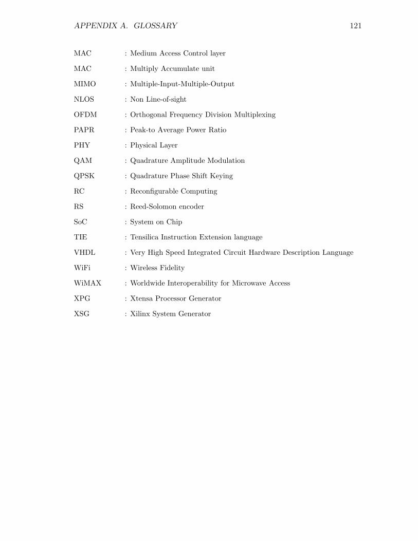
APPENDIX A. GLOSSARY 121
MAC : Medium Access Control layer
MAC : Multiply Accumulate unit
MIMO : Multiple-Input-Multiple-Output
NLOS : Non Line-of-sight
OFDM : Orthogonal Frequency Division Multiplexing
PAPR : Peak-to Average Power Ratio
PHY : Physical Layer
QAM : Quadrature Amplitude Modulation
QPSK : Quadrature Phase Shift Keying
RC : Reconfigurable Computing
RS : Reed-Solomon encoder
SoC : System on Chip
TIE : Tensilica Instruction Extension language
VHDL : Very High Speed Integrated Circuit Hardware Description Language
WiFi : Wireless Fidelity
WiMAX : Worldwide Interoperability for Microwave Access
XPG : Xtensa Processor Generator
XSG : Xilinx System Generator
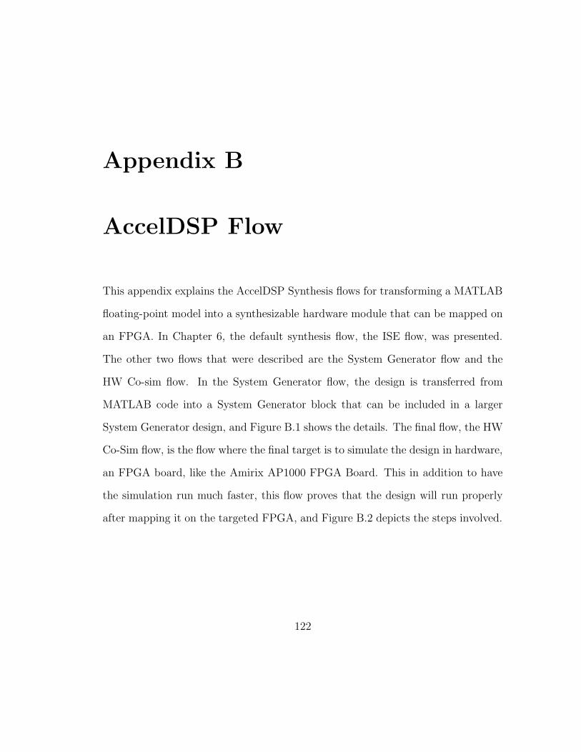
Appendix B
AccelDSP Flow
This appendix explains the AccelDSP Synthesis flows for transforming a MATLAB
floating-point model into a synthesizable hardware module that can be mapped on
an FPGA. In Chapter 6, the default synthesis flow, the ISE flow, was presented.
The other two flows that were described are the System Generator flow and the
HW Co-sim flow. In the System Generator flow, the design is transferred from
MATLAB code into a System Generator block that can be included in a larger
System Generator design, and Figure B.1 shows the details. The final flow, the HW
Co-Sim flow, is the flow where the final target is to simulate the design in hardware,
an FPGA board, like the Amirix AP1000 FPGA Board. This in addition to have
the simulation run much faster, this flow proves that the design will run properly
after mapping it on the targeted FPGA, and Figure B.2 depicts the steps involved.
122

APPENDIX B. ACCELDSP FLOW 123
Figure B.1: The AccelDSP System Generator Synthesis Flow

APPENDIX B. ACCELDSP FLOW 124
Figure B.2: The AccelDSP HW Co-sim Synthesis Flow

Appendix C
IEEE 802.16-2004 Standard
In this appendix few details about the standard document will be presented. The
details include a sample of the test benches used and the mapping constellations.
C.1 Example of an OFDM uplink
The following vectors illustrate the results obtained after each process, starting
from randomization through subcarrier modulation. The presented data is in hex-
adecimal notation, and it represents the case of a modulation scheme of QPSK and
a coding rate of 3/4.
Input Data
45 29 C4 79 AD 0F 55 28 AD 87 B5 76 1A 9C 80 50 45 1B 9F D9 2A 88 95 EB
AE B5 2E 03 4F 09 14 69 58 0A 5D
Randomized Data
D4 BA A1 12 F2 74 96 30 27 D4 88 9C 96 E3 A9 52 B3 15 AB FD 92 53 07 32 C0
125
APPENDIX C. IEEE 802.16-2004 STANDARD 126
62 48 F0 19 22 E0 91 62 1A C1
Reed-Solomon encoded Data
49 31 40 BF D4 BA A1 12 F2 74 96 30 27 D4 88 9C 96 E3 A9 52 B3 15 AB FD 92
53 07 32 C0 62 48 F0 19 22 E0 91 62 1A C1 00
Convolutionally Encoded Data
3A 5E E7 AE 49 9E 6F 1C 6F C1 28 BC BD AB 57 CD BC CD E3 A7 92 CA 92
C2 4D BC 8D 78 32 FB BF DF 23 ED 8A 94 16 27 A5 65 CF 7D 16 7A 45 B8 09
CC
Interleaved Data
77 FA 4F 17 4E 3E E6 70 E8 CD 3F 76 90 C4 2C DB F9 B7 FB 43 6C F1 9A BD
ED 0A 1C D8 1B EC 9B 30 15 BA DA 31 F5 50 49 7D 56 ED B4 88 CC 72 FC 5C
Subcarrier Mapping (frequency offset index: I value Q value)
-100: 1 -1, -99: -1 -1, -98: 1 -1, -97: -1 -1, -96: -1 -1, -95: -1 -1, -94: -1 1, -93: -1 1,
-92: 1 -1, -91: 1 1,-90: -1 -1, -89: -1 -1, -88:pilot= 1 0, -87: 1 1, -86: 1 -1, -85: 1
-1, -84: -1 -1, -83: 1 -1, -82: 1 1, -81: -1 -1,-80: -1 1, -79: 1 1, -78: -1 -1, -77: -1 -1,
-76: -1 1, -75: -1 -1, -74: -1 1, -73: 1 -1, -72: -1 1, -71: 1 -1,-70: -1 -1, -69: 1 1, -68:
1 1, -67: -1 -1, -66: -1 1, -65: -1 1, -64: 1 1, -63:pilot= -1 0, -62: -1 -1, -61: 1 1,-60:
-1 -1, -59: 1 -1, -58: 1 1, -57: -1 -1, -56: -1 -1, -55: -1 -1, -54: 1 -1, -53: -1 -1, -52:
1 -1, -51: -1 1,-50: -1 1, -49: 1 -1, -48: 1 1, -47: 1 1, -46: -1 -1, -45: 1 1, -44: 1 -1,
-43: 1 1, -42: 1 1, -41: -1 1,-40: -1 -1, -39: 1 1, -38:pilot= 1 0, -37: -1 -1, -36: 1 -1,
-35: -1 1, -34: -1 -1, -33: -1 -1, -32: -1 -1, -31: -1 1,-30: 1 -1, -29: -1 1, -28: -1 -1,
-27: 1 -1, -26: -1 -1, -25: -1 -1, -24: -1 -1, -23: -1 1, -22: -1 -1, -21: 1 -1,-20: 1 1,
-19: 1 1, -18: -1 -1, -17: 1 -1, -16: -1 1, -15: -1 -1, -14: 1 1, -13:pilot= -1 0, -12: -1

APPENDIX C. IEEE 802.16-2004 STANDARD 127
-1, -11: -1 -1,-10: 1 1, -9: 1 -1, -8: -1 1, -7: 1 -1, -6: -1 1, -5: -1 1, -4: -1 1, -3: -1
-1, -2: -1 -1, -1: 1 -1,0: 0 0, 1: -1 -1, 2: -1 1, 3: -1 -1, 4: 1 -1, 5: 1 1, 6: 1 1, 7: -1
1, 8: -1 1, 9: 1 1,10: 1 -1, 11: -1 -1, 12: 1 1, 13:pilot= 1 0, 14: -1 -1, 15: 1 -1, 16:
-1 1, 17: 1 1, 18: 1 1, 19: 1 -1,20: -1 1, 21: -1 -1, 22: -1 -1, 23: -1 1, 24: -1 -1, 25:
1 1, 26: -1 1, 27: 1 -1, 28: -1 1, 29: -1 -1,30: 1 1, 31: -1 -1, 32: 1 1, 33: 1 1, 34: 1
1, 35: 1 -1, 36: 1 -1, 37: 1 -1, 38:pilot= 1 0, 39: -1 1,40: -1 -1, 41: -1 1, 42: -1 1,
43: -1 -1, 44: 1 -1, 45: -1 1, 46: -1 1, 47: 1 1, 48: -1 -1, 49: 1 1,50: 1 -1, 51: -1 -1,
52: -1 -1, 53: 1 -1, 54: 1 -1, 55: 1 -1, 56: 1 -1, 57: 1 1, 58: 1 1, 59: 1 -1,60: 1 1, 61:
-1 1, 62: 1 -1, 63:pilot= 1 0, 64: 1 -1, 65: -1 -1, 66: -1 -1, 67: 1 -1, 68: 1 -1, 69: 1
-1,70: 1 -1, 71: -1 1, 72: -1 -1, 73: -1 1, 74: -1 -1, 75: 1 -1, 76: -1 1, 77: -1 -1, 78: 1
-1, 79: 1 1,80: -1 1, 81: 1 1, 82: -1 1, 83: 1 1, 84: -1 -1, 85: 1 1, 86: -1 -1, 87: 1 1,
88:pilot= 1 0, 89: 1 -1,90: -1 -1, 91: 1 1, 92: -1 1, 93: -1 -1, 94: -1 -1, 95: -1 -1, 96:
1 1, 97: 1 -1, 98: 1 -1, 99: -1 -1, 100: 1 1
The values after performing the subcarrier mapping still to be multiplied by a
factor of 1/√
2 for QPSK modulation.
C.2 Constellations
After performing the interleaving step, the interleaved data bits are fed serially
to the mapper to map each group of bits (1,2,4 or 6) to the corresponding I/Q
pairs depending on the modulation scheme. These I/Q pairs are normalized with
a factor c, again depending on the modulation scheme. The constellations for the
four modulation schemes are shown in Figure C.1, where b0 denotes the LSB.
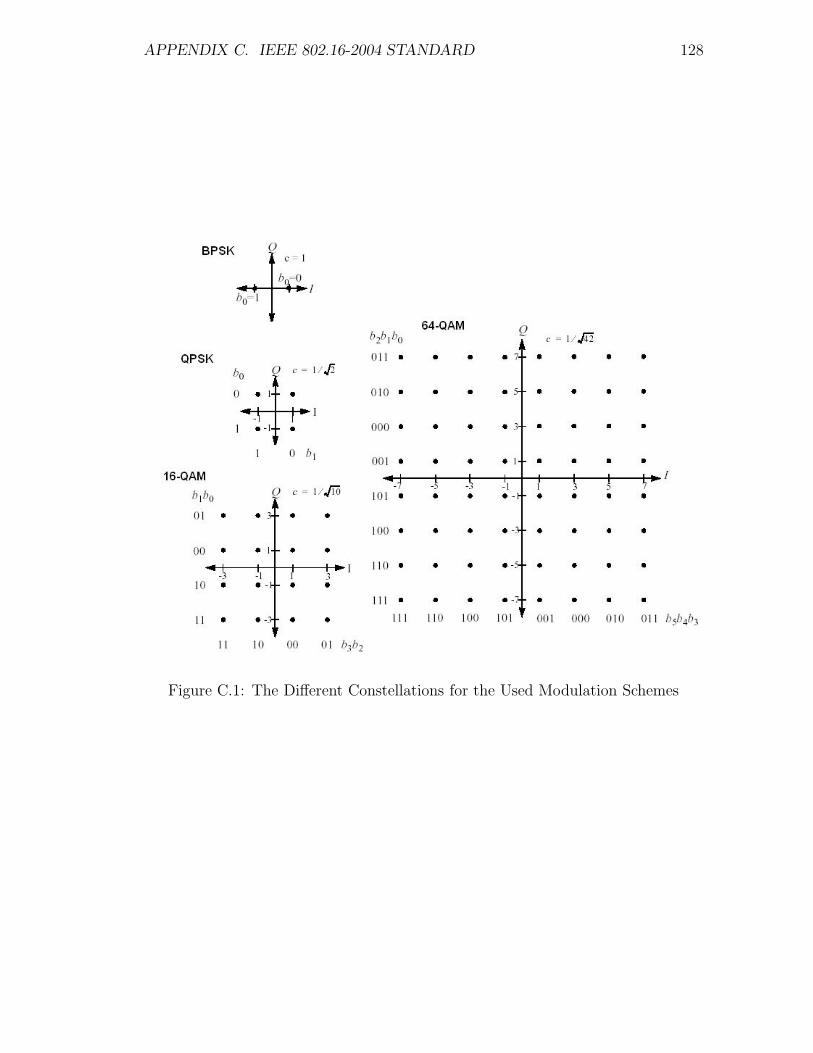
APPENDIX C. IEEE 802.16-2004 STANDARD 128
Figure C.1: The Different Constellations for the Used Modulation Schemes