Dynamically reconfigurable integrated optical...
8
Dynamically reconfigurable integrated optical circulators DUANNI HUANG, 1, * ,† PAOLO PINTUS, 1,2,† CHONG ZHANG, 1 PAUL MORTON, 3 YUYA SHOJI, 4 TETSUYA MIZUMOTO, 4 AND JOHN E. BOWERS 1 1 Electrical and Computer Engineering Department, University of California Santa Barbara, California 93106, USA 2 Scuola Superiore Sant’Anna, via Moruzzi 1, 56124 Pisa, Italy 3 Morton Photonics, 3301 Velvet Valley Dr, West Friendship, Maryland 21794, USA 4 Department of Electrical and Electronic Engineering/FIRST, Tokyo Institute of Technology, Tokyo, Japan *Corresponding author: [email protected] Received 16 September 2016; revised 16 November 2016; accepted 29 November 2016 (Doc. ID 275809); published 21 December 2016 Optical circulators that unidirectionally route light could lead to bidirectional operations in applications in data centers and telecommunications, as well as sensors. In this work, to the best of our knowledge, we present the first realization of integrated optical circulators on silicon that are electrically driven and dynamically reconfig- urable. The proposed device utilizes silicon microrings with a bonded magneto-optic cladding alongside an integrated electromagnet for nonreciprocal behavior. This novel approach does not use a permanent magnet and, for this reason, it is more attractive for packaging and further integration with lasers and other photonic devices. We use this device architecture to demonstrate 4- and 6-port optical circulators with up to 14.4 dB of isolation and propose a framework to extend the design to an arbitrary number of ports. Finally, we demonstrate that it is possible to switch the electro- magnet and reconfigure the circulator on a sub-nanosecond timescale, potentially adding a new level of device functionality. © 2016 Optical Society of America OCIS codes: (230.3240) Isolators; (230.3810) Magneto-optic systems; (230.5750) Resonators; (130.3120) Integrated optics devices. https://doi.org/10.1364/OPTICA.4.000023 1. INTRODUCTION Optical isolators and circulators are nonreciprocal devices that allow for the unidirectional propagation of light [1]. Optical isolators are two-port devices that serve as a one-way street for photons and are crucial in preventing undesired back-reflections from interacting with a laser. Expanding on this analogy, optical circulators are many-port devices that act as a roundabout for photons, with each input port routed to exactly one output port in a nonreciprocal fashion. Integrated circulators would enable bidirectional operations in optical interconnects [2–4], which could double the network capacity in many data center and tele- communication applications [5]. They are also important compo- nents in many distributed fiber sensors and other interferometric optical sensors [6]. Achieving the necessary optical nonreciprocity on chip is a challenging task, and various approaches have been investigated using spatial-temporal, electro-optic-based modulation [7–13], as well as optical nonlinearities such as stimulated Brillouin scatter- ing [14,15]. Thermo-optic and Kerr-like nonlinearities have also been used to make optical diodes [16,17], although dynamic reci- procity may prevent them from functioning as isolators [18]. While these methods are attractive since they only require Si or III–V materials, they rely on fairly weak effects and have been limited in isolation or intrinsically have high losses. In some cases, they also require multiple modulators with high-speed electronic drive signals and additional optical filters, which can significantly increase the footprint and complexity of the device [12,13]. On the other hand, the magneto-optic Faraday effect provides a simple, straightforward path toward nonreciprocity and is widely used in fiber and bulk-optic circulators today. However, the transition to integrated photonics has been challenging due to severe lattice and thermal mismatch between commonly used magneto-optic materials, such as cerium-substituted yttrium iron garnet (Ce:YIG) and Si or III–V substrates [19]. Recently, there have been several works that investigated pulsed laser deposition or sputtering of magneto-optic garnets on silicon [20–23]. While these methods show great promise as a monolithic technology, they require the presence of a virtual substrate or buffer layer, as well as a high-temperature, rapid thermal anneal (>700°C) to promote the crystallization of the magneto-optic garnets. An alternate approach to integrating magneto-optic garnets onto silicon substrates is heterogeneous integration using wafer bond- ing techniques, which can circumvent the lattice mismatch issue [24]. Heterogeneous integration has been used to integrate vastly different materials, including III–V’ s, LiNbO 3 , and Ce:YIG on silicon-on-insulator (SOI) substrates in order to obtain optical gain and efficient nonlinear effects, as well as the desired optical nonreciprocity for silicon photonics [25,26]. In this approach, the 2334-2536/17/010023-08 Journal © 2017 Optical Society of America Research Article Vol. 4, No. 1 / January 2017 / Optica 23
Transcript of Dynamically reconfigurable integrated optical...
Dynamically reconfigurable integrated opticalcirculatorsDUANNI HUANG,1,*,† PAOLO PINTUS,1,2,† CHONG ZHANG,1 PAUL MORTON,3 YUYA SHOJI,4
TETSUYA MIZUMOTO,4 AND JOHN E. BOWERS1
1Electrical and Computer Engineering Department, University of California Santa Barbara, California 93106, USA2Scuola Superiore Sant’Anna, via Moruzzi 1, 56124 Pisa, Italy3Morton Photonics, 3301 Velvet Valley Dr, West Friendship, Maryland 21794, USA4Department of Electrical and Electronic Engineering/FIRST, Tokyo Institute of Technology, Tokyo, Japan*Corresponding author: [email protected]
Received 16 September 2016; revised 16 November 2016; accepted 29 November 2016 (Doc. ID 275809); published 21 December 2016
Optical circulators that unidirectionally route light could lead to bidirectional operations in applications indata centers and telecommunications, as well as sensors. In this work, to the best of our knowledge, we presentthe first realization of integrated optical circulators on silicon that are electrically driven and dynamically reconfig-urable. The proposed device utilizes silicon microrings with a bonded magneto-optic cladding alongside an integratedelectromagnet for nonreciprocal behavior. This novel approach does not use a permanent magnet and, for this reason,it is more attractive for packaging and further integration with lasers and other photonic devices. We use this devicearchitecture to demonstrate 4- and 6-port optical circulators with up to 14.4 dB of isolation and propose a frameworkto extend the design to an arbitrary number of ports. Finally, we demonstrate that it is possible to switch the electro-magnet and reconfigure the circulator on a sub-nanosecond timescale, potentially adding a new level of devicefunctionality. © 2016 Optical Society of America
OCIS codes: (230.3240) Isolators; (230.3810) Magneto-optic systems; (230.5750) Resonators; (130.3120) Integrated optics devices.
https://doi.org/10.1364/OPTICA.4.000023
1. INTRODUCTION
Optical isolators and circulators are nonreciprocal devices thatallow for the unidirectional propagation of light [1]. Opticalisolators are two-port devices that serve as a one-way street forphotons and are crucial in preventing undesired back-reflectionsfrom interacting with a laser. Expanding on this analogy, opticalcirculators are many-port devices that act as a roundabout forphotons, with each input port routed to exactly one output portin a nonreciprocal fashion. Integrated circulators would enablebidirectional operations in optical interconnects [2–4], whichcould double the network capacity in many data center and tele-communication applications [5]. They are also important compo-nents in many distributed fiber sensors and other interferometricoptical sensors [6].
Achieving the necessary optical nonreciprocity on chip is achallenging task, and various approaches have been investigatedusing spatial-temporal, electro-optic-based modulation [7–13], aswell as optical nonlinearities such as stimulated Brillouin scatter-ing [14,15]. Thermo-optic and Kerr-like nonlinearities have alsobeen used to make optical diodes [16,17], although dynamic reci-procity may prevent them from functioning as isolators [18].While these methods are attractive since they only require Sior III–V materials, they rely on fairly weak effects and have beenlimited in isolation or intrinsically have high losses. In some cases,
they also require multiple modulators with high-speed electronicdrive signals and additional optical filters, which can significantlyincrease the footprint and complexity of the device [12,13].
On the other hand, the magneto-optic Faraday effect providesa simple, straightforward path toward nonreciprocity and iswidely used in fiber and bulk-optic circulators today. However,the transition to integrated photonics has been challenging dueto severe lattice and thermal mismatch between commonly usedmagneto-optic materials, such as cerium-substituted yttrium irongarnet (Ce:YIG) and Si or III–V substrates [19]. Recently, therehave been several works that investigated pulsed laser depositionor sputtering of magneto-optic garnets on silicon [20–23]. Whilethese methods show great promise as a monolithic technology,they require the presence of a virtual substrate or buffer layer,as well as a high-temperature, rapid thermal anneal (>700°C)to promote the crystallization of the magneto-optic garnets.An alternate approach to integrating magneto-optic garnets ontosilicon substrates is heterogeneous integration using wafer bond-ing techniques, which can circumvent the lattice mismatch issue[24]. Heterogeneous integration has been used to integrate vastlydifferent materials, including III–V’s, LiNbO3, and Ce:YIG onsilicon-on-insulator (SOI) substrates in order to obtain opticalgain and efficient nonlinear effects, as well as the desired opticalnonreciprocity for silicon photonics [25,26]. In this approach, the
2334-2536/17/010023-08 Journal © 2017 Optical Society of America
Research Article Vol. 4, No. 1 / January 2017 / Optica 23
magneto-optic material (Ce:YIG) is grown on a lattice matched(Ca, Mg, Zr) -substituted gadolinium gallium garnet (SGGG)substrate and then bonded on silicon waveguides. Several isolatorsand circulators have been demonstrated with this approach[27–35], which does not require a high temperature anneal andis compatible with multiple die bonding techniques for high-performance photonic-integrated circuits.
In this paper, we demonstrate heterogeneously integrated op-tical circulators on silicon operating in the transverse magnetic(TM) mode with up to 14.4 dB of isolation ratio. Unlike previousintegrated circulators that utilize an asymmetric Mach–Zehnderinterferometer (MZI) structure [28–32], we exploit a microring-based structure with a significantly reduced footprint (20 μmradius). Furthermore, we do not use a permanent magnet togenerate the magnetic field. Instead, a localized magnetic fieldis generated from an integrated microstrip that serves as anelectromagnet and can be tailored to match various device geom-etries. This current-induced magnetic field can be switched with arise and fall time of 400 ps, which flips the direction of the mag-netic field and reroutes all the optical pathways in the device.Thus, the circulator can be dynamically reconfigured on a sub-nanosecond timescale. Finally, we demonstrate that this designfor a 4-port circulator can be cascaded to realize a 6-port circulatorwith four different working configurations. We can achieve anarbitrary number of ports by expanding this device architectureeven further, which may lead to novel reconfigurable optical net-works and switches on-chip.
2. DEVICE OVERVIEW
A variety of optical isolators and circulators have been demon-strated based on different magneto-optic related phenomenon,ranging from TE–TM mode conversion to nonreciprocal lossand phase shift. Of all these approaches, the nonreciprocal phaseshift (NRPS) effect has been the most widely used of late, as itdoes not require the tight fabrication accuracy necessary for phasematching in mode conversion. A nonreciprocal phase shift is afirst-order effect that occurs when light flows through a mag-neto-optic medium that is magnetized perpendicular to the direc-tion of light propagation, also known as the Voigt configuration.Depending on whether the magnetic field is in-plane or out-of-plane with respect to the waveguide, NRPS is achieved for theTM and TE modes, respectively [35]. In the TM case, themagneto-optic material serves as a top cladding (or bottomcladding) for the waveguide, while the magnetic field is in-planeand transverse to the light propagation direction. Under thesecircumstances, the propagation constants of the forward (β�)and backward (β−) propagating light in the waveguide are differ-ent. The sign of the difference in the propagation constant(Δβ � β� − β−) is dependent on the direction of magnetizationwith respect to the propagation. Therefore, if the magnetizationdirection is flipped, we obtain the opposite sign on Δβ, as ifβ� and β− are interchanged due to a change in the propagationdirection. This is the operating principle behind reconfigurabilityin this work. Isolation for the TE mode can be achieved by using apolarization rotator before the TM mode isolator [33] or byachieving a structure in which the magneto-optic material islaterally adjacent to the waveguide [35].
In order to achieve optical isolation and circulation based onthe NRPS, a phase-sensitive structure, such as an MZI or a mi-croring, is needed. Previous experiments have shown high optical
isolation as well as successful circulation using an asymmetricMZI in which there is a �π∕2 NRPS on one arm accordingto the direction of propagation, such that it interferes construc-tively (forward) and destructively (backward) with the reciprocalarm, which is set at a phase bias of 2mπ � π∕2. Depending on theinteger value ofm, the free spectral range (FSR) of the MZI can beadjusted, and thus, the 20 dB bandwidth can be set to be as wideas 8 nm [28]. A disadvantage of this device is an enlarged foot-print, since the length of magneto-optic interaction in the wave-guide required for π∕2 NRPS is typically hundreds of microns[30] to several millimeters long [33], depending on the exactwaveguide geometry. On the other hand, a miniaturized footprintis one of the main reasons the ring resonator has been so widelystudied over the past decade. This footprint reduction plays anespecially important role in magneto-optic devices due to the lossynature of Ce:YIG (∼40–60 dB∕cm) [19,28] and other magneto-optic materials, such as cobalt ferrites (∼dB∕μm) [36]. Thus, amicroring structure has great potential to reduce the insertion lossof the device by reducing the footprint. We have previously dem-onstrated this concept in a microring isolator with 32 dB of iso-lation and only 2.3 dB of excess loss to silicon [37,38]. Microringscome with an inherent drawback of limited bandwidth. However,this may be improved with the design of coupled or cascaded ringfilters.
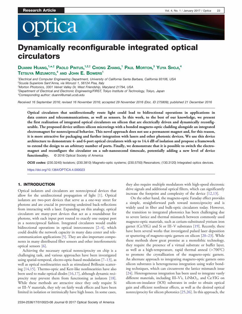
In a microring isolator or circulator, the magneto-opticCe:YIG serves as an upper cladding over the ring, and the appliedmagnetic field must be either radially inward or outward with re-spect to the ring in order to achieve NRPS for the TMmode. Thedifference in propagation constants causes a resonance wavelengthsplit between the clockwise (CW) and counterclockwise (CCW)modes in the resonator. The magnitude of this resonance wave-length split (RWS) is dependent on the strength of the magneticfield below magnetic saturation, as well as the waveguide geom-etry. For an optical circulator, we utilize the microring in an add–drop filter configuration, as shown below, in Fig. 1. Here, we haveshown the two scenarios where the magnetic field is pointing ra-dially inward (top) or outward (bottom). The port that is used asthe input will determine the propagation direction of light andtherefore whether we couple to the CW or CCW mode inthe ring.
Fig. 1. We depict the spectrum of the through port of the ring for thetwo operating configurations of the circulator. Light entering from port 1will couple into the CW mode (the transmittance spectrum is plotted inthe red dashed line) and light entering from port 2 will couple into theCCW mode (the transmittance spectrum is plotted in the blue continu-ous line). For the sake of simplicity, we do not depict the transmittancespectrum at the drop port, as it can be assumed to have the same resonantcharacteristics. By flipping the magnetic field, the circulation is reversedat the same operating wavelength.
Research Article Vol. 4, No. 1 / January 2017 / Optica 24
In Fig. 1, we align the operating wavelength to the CCWresonance of the ring. Under these conditions, the wavelengthof light entering from port 1 (red arrow) is not aligned withthe ring resonance, and therefore, the light passes through toport 2. Meanwhile, light injected from port 2 (blue arrow) excitesthe CW ring resonance, and it will be dropped to port 3.Thus, the circulation direction in this configuration is1 → 2 → 3 → 4 → 1. If the magnetic field is flipped to a radiallyoutward direction, as shown in the bottom half of Fig. 1, thesame operating wavelength is now aligned to the CW resonance.In this alternate configuration, the light circulates from1 → 4 → 3 → 2 → 1. As long as the magnetic field can bereliably switched, the circulator can be reconfigured. This equiv-alence between switching the propagation direction and switchingthe current direction is confirmed in the Supplement 1.
Conventionally, isolators and circulators are packaged withsmall, permanent magnets (∼mm2 to cm2) that provide the nec-essary magnetization of the material. However, it is difficult togenerate radially orientated magnetic fields over a small microringusing permanent magnets and even more difficult to switch themagnetization. Special care must also be taken in the packaging ofthese magnets, and they remain a discrete component in anotherwise fully integrated device. There has been prior researchinvolving the use of thin-film permanent magnets for opticalisolators [39], but this does not address the issue of generatinga radial magnetic field. Instead, we use an integrated metallic mi-crostrip that is on top of the garnet cladding, which serves as anelectromagnet. The current applied through this microstrip willgenerate a local magnetic field in the magneto-optic material (i.e.,the waveguide top cladding) and can be easily switched to realizethe aforementioned reconfigurability. The microstrip can followthe shape of any waveguide structure, whether it is the microringshown here or an MZI device, and it can be designed to providethe desired magnetic field profile. Finally, this approach is muchmore suitable for packaging and co-integration with integratedelectronic circuits and drivers.
3. DEVICE DESIGN AND FABRICATION
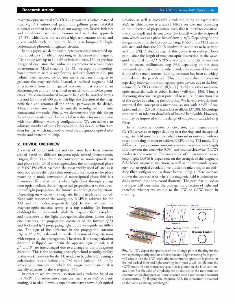
The ring resonator is designed with a cross section that optimizesthe RWS under a transverse magnetic field, while maintainingsingle-mode operation for TM modes [40]. For the optimization,we use a finite element nonreciprocal mode solver to accuratelycalculate the NRPS for a given waveguide geometry [41]. The4-port circulator in this paper consists of an add–drop ring res-onator filter with a radius of 20 μm and is depicted below inFig. 2(a). The ring radius is chosen to avoid bending loss, as theoptical confinement in the silicon is lower due to the presence of amagneto-optic garnet cladding, as shown in Fig. 2(b). The reso-nator is fabricated on a silicon-on-insulator (SOI) wafer usingDUV lithography, and then the Ce:YIG (n � 2.2) on SGGG(n � 1.97) die is directly bonded on top of the microring usingan O2 plasma assisted bonding process. The bond is annealed at200°C under 3 MPa of pressure to strengthen the bond. Next, thebackside of the bonded die is thinned down to roughly 8 μm us-ing mechanical polishing. Finally, the integrated electromagnet isfabricated by depositing a 1.5 μm thick gold microstrip on thebackside of the bonded die, as depicted in the microscope imagein Fig. 2(c).
The input/output relation of the 4-port device can beeffectively described by the scattering matrix
0BB@
A−1
A−2
A−3
A−4
1CCA �
0BB@
0 S12 0 S14S21 0 S23 00 S32 0 S34S41 0 S43 0
1CCA
0BB@
A�1
A�2
A�3
A�4
1CCA; (1)
where A−i (for I � 1, 2, 3, 4) represents the amplitude of the out-
put light, and A�j (for j � 1, 2, 3, 4) is the amplitude of the input
light. We assume that the backscattering caused by the waveguideroughness is negligible, so the scattering coefficients along thediagonal are set equal to zero. For the same reason, the lightinjected from port 1 can only propagate through port 2 and port4 but not to port 3, which implies S31 � 0. With similar argu-ments, S24 � S13 � S42 � 0. Moreover, if the two waveguideshave symmetric coupling with the microring, the following iden-tity is held, and only four scattering coefficients are needed:
S12 � S34; S14 � S32; S41 � S23; S43 � S21:(2)
It is worth noting that the scattering matrix is asymmetric dueto nonreciprocity and Sij�λ� ≠ Sji�λ�. Instead, the spectra for thenonzero coefficients are related by the following relation,
Sij�λ� ΔλMO∕2� � Sji�λ� ΔλMO∕2�; (3)
where ΔλMO is the resonance wavelength split in the ring, and thesign in the argument must be chosen according to the direction ofthe external magnetic field. As with any microring, a key param-eter in determining the scattering matrix is the waveguide ringcoupling power (K ). In our design, we have fixed K to be10.45%, in order to achieve equal isolation ratios among allthe ports, which is described in more detail in the Supplement 1.
As described in Fig. 2, a gold microstrip coil was deposited toserve as the electromagnet. In order to provide a large magneticfield while limiting heating, a large current and a small resistanceare required. Therefore, the gold microstrip cross section is set tobe 3 μm wide and 1.5 μm thick, with a measured resistivity near1 Ohm. Simulations using COMSOL multiphysics for magneticand thermal properties are shown in Fig. 3. The plots depict theradial component of the magnetic field (Hr) in the CeYIG layerabove the ring and the average temperature increment (ΔT ) inthe silicon ring as a function of the current in the coil. As weexpected, the field Hr varies linearly with the current, whileΔT is a quadratic function of the current due to the Joule effect.
Fig. 2. (a) 3D prospective view of the device, (b) cross-sectional modeprofile, and (c) microscope image of the fabricated device. The siliconwaveguide is 230 nm tall and 600 nm wide, and the Ce:YIG is400 nm thick. A thin layer of silica (∼10 nm) is assumed to have formedbetween the waveguide and the bonded layer due to the plasma activa-tion [24].
Research Article Vol. 4, No. 1 / January 2017 / Optica 25

These simulations are key to understanding the behavior of thecirculator at different driving currents.
4. EXPERIMENTAL RESULTS
We characterize the device at room temperature (20°C) usinga polarization-maintaining (PM) lensed fiber to injectTM-polarized light. Then, we measure the transmittance spectrathrough the device at the output ports when we apply −200 mAof current through the microstrip. This corresponds to roughly40 mW of dissipated power in the microstrip. This may be im-proved by using a larger gold cross section, thinning the SGGG
further, or depositing multiple coils of the electromagnet. Furtherdetails on the experimental setup can be found in the Supplement1. The experimental results are shown in Fig. 4(a), where all thespectra have been normalized to a reference silicon waveguide ofthe same dimension but covered by a silica top cladding instead ofthe Ce:YIG. For comparison, the simulated spectra are reportedin Fig. 4(b). The simulated and measured scattering coefficientsexhibit a good agreement between the theory and the experi-ments, confirming the validity of our model.
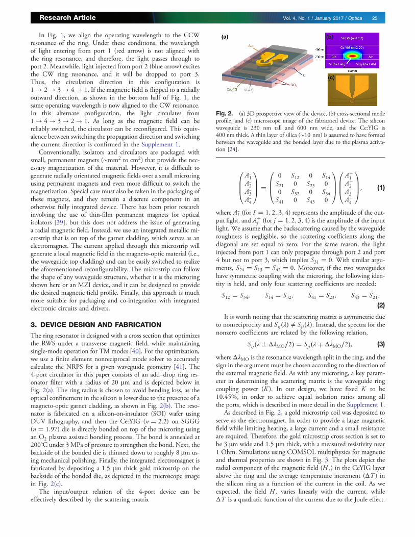
Because the bonded chip is 3.5 mm long, the propagation lossin the input/output waveguide is estimated to be 8.7 dB due tothe absorption of the Ce:YIG (∼40–60 dB/cm), where the modeoverlap is computed to be about 41%. The measured wavelengthsplit between the CW (red) and CCW (blue) resonances inFig. 4(a) is measured to be 0.35 nm. This value is smaller thanthe simulated maximum of 0.55 nm because the magnetic field isbelow the saturation value for the Faraday rotation (i.e., 50 Oe) aswell as a temperature-induced reduction of the magneto-opticeffect [38,42]. In Fig. 5, the nonreciprocal resonance split (MO)and the reciprocal shift (Therm.) are shown as functions of theinjected current. The values predicted by our model and the mea-sured ones show a very good agreement between the theory andthe experiments.
If we choose to operate near λ � 1558.45 nm, denoted by thedashed black line in Fig. 4(a), then the light in the device circu-lates from 1 → 2 → 3 → 4 → 1. From these measurements, weare able to summarize the performance of the 4-port circulator asshown in Table 1, where the amplitudes of the scattering coef-ficients are reported at the working wavelength. The missingentries are paths that are only obtainable due to strong back-reflections. We were unable to quantitatively measure the valuesof S13, S31, S24, and S42, as they are very low (less than −40 dB).Likewise, the measurement to quantify the backscattered light ateach port (Sii, for I � 1, 2, 3, 4) is dominated by reflections offthe polished facet as well as the lensed fiber used for the coupling.
In this table, the highlighted entries depict the insertion lossfor the forward circulating path and range from 9.7 to 12.4 dB.Such large values are due to the Ce:YIG clad bus waveguides
Fig. 3. (a) Radial magnetic field map (in Oersted) in the Ce:YIG layerfor an injected current I � 200 mA (V � 190 mV), as well as its lineardependence with the injected current. (b) Temperature variation (inCelsius) in the silicon layer for an injected current I � 200 mA, andits quadratic dependence with the injected current. For the device undertest, a current of 200 mA provides a radial magnetic field of about 17 Oein the Ce:YIG layer, while the temperature increment is about 10°C inthe silicon microring.
Fig. 4. (a) Measured and (b) simulated transmission spectra of the CW and CCW resonances at the through and drop ports. The curves are labeled by thecorresponding entry in the scattering matrix. Due to fabrication inaccuracies in the waveguide, the measured spectra are shifted with respect to the measuredones. The thermal heating can be effectively used to control the resonance position, compensating the variation of the waveguide cross-section size.
Research Article Vol. 4, No. 1 / January 2017 / Optica 26
(3.5 mm), which are much longer than the actual microring size(i.e., 20 μm radius) and can be reduced by shrinking the die sizeor using transitions to push the mode away from the Ce:YIG. Wedo not notice any increase in the insertion loss due to themagnetic field or heating of the device.
As formerly stated, the isolation ratio is defined as the ratio offorward to backward transmitted power between two adjacentports. The largest isolation ratio is 11 dB, and it is measured be-tween port 1 and port 2, and between port 3 and port 4 (i.e., IR12
and IR34). Vice versa, the smallest isolation ratio is 6.7 dB that ismeasured between port 1 and port 4 (i.e., IR14). Another impor-tant key feature to evaluate the performance of the device is thecrosstalk at the output port (XT). It can be defined as the ratiobetween the sum of transmitted signal powers from all undesiredports and the transmitted signal power from the desired outputport. From Table 1, it is calculated as the difference between theentries in any horizontal row. The crosstalk in this device rangesfrom −6.2 dB at port 4 to −11.3 dB at port 2. The results aresummarized below in Table 2. The measured IRs are smaller thanthe simulated values because the device is operating below thesaturation magnetization value (ΔλMO < 0.55 nm), as shownin the table.
Both the isolation ratio and the crosstalk of the device can beimproved by increasing the RWS and differentiating the CW andCCW resonance even further. However, more current is needed,and that can produce larger heating and eventually damage thedevice. To avoid this issue, we plan to use multiple coils forthe electromagnet, allowing for higher magnetic fields at a loweroperating current and temperature [43].
We also investigate the switching time of the device, or thetime it takes to reconfigure the circulator. The wavelength is setto bias the ring at the side of the resonance for higher modulation
efficiency, and the input is a zero-mean signal such that thetemperature remains constant for the device. To test the rise timeof the magneto-optic response, a pseudo-random bit sequence(PRBS31) with 1.5 Vpp and no DC bias is applied to the electro-magnet, while an optical signal is injected from port 1 and theoutput light at port 2 is collected on a sampling oscilloscope.For a PRBS at 1 Gbps, the resulting eye diagram is shown inFig. 6, where we measure a 400 ps rise time with an 8.5 dBextinction ratio.
In this experiment, the magneto-optic response is limited bythe rising impedance of the electromagnet at higher frequencies,which acts as an inductor. Nevertheless, it is significantly fasterthan the slow thermal-controlled microrings that are being uti-lized for large-scale photonic switching fabrics [44]. Faster oper-ation can be achieved by reducing skin depth effects and loweringthe inductance of the microstrip, although additional limitationscaused by magnetization reversal (∼2 ps) [45] and photon life-time (∼12 ps) in the ring will eventually become relevant.
5. MULTIPLE PORT (>4) CIRCULATORS
The demonstrated 4-port circulator can be used as a buildingblock for more complex nonreciprocal devices and networks.Here, we demonstrate how our device design can be expandedto realize circulators with an arbitrary number of input/outputports. We will only consider devices using the microring architec-ture; nevertheless, the principles shown here can be carried overto design multi-port MZI circulators as well. In this section,
Fig. 5. Measured and predicted reciprocal resonance shift (thermaleffect) and nonreciprocal resonance split (MO effect) have been reportedas a function of the applied current.
Table 1. Experimental Transmittance Data [dB] of theCirculator at theWorkingWavelength of λ � 1558.45 nm
Input Port
Output Port
1 2 3 41 – −20.7 – −10.52 −9.7 – −21.0 –3 – −12.4 – −22.04 −17.2 – −11.0 –
Table 2. Simulated and Experimental Isolation Ratio andCrosstalka at theWorkingWavelength of λ � 1558.45 nm forDifferent Values of ΔλMO [nm]
ΔλMO � 0.55(Simulated)
ΔλMO � 0.35(Simulated)
ΔλMO � 0.35(Experiment)
IR12 � jS21j2∕jS12j2 12.0 dB 11.6 dB 11.0 dBIR23 � jS32j2∕jS23j2 12.0 dB 8.5 dB 8.6 dBIR34 � jS43j2∕jS34j2 12.0 dB 11.6 dB 11.0 dBIR41 � jS14j2∕jS41j2 12.0 dB 8.5 dB 6.7 dBXT1 � jS12j2∕jS14j2 −14.3 dB −10.18 dB −10.2 dBXT2 � jS23j2∕jS21j2 −10.0 dB −10.0 dB −11.3 dBXT3 � jS34j2∕jS32j2 −14.3 dB −10.18 dB −9.6 dBXT4 � jS41j2∕jS43j2 −10.0 dB −10.0 dB −6.2 dB
aThe crosstalk is calculated assuming equal input powers at each port.
Fig. 6. Magneto-optic rise time of the device is measured to be 400 psusing a 1 Gbps PRBS31 bit stream. The eye stays open up to 2.5 Gbps,which agrees well with the measured rise time.
Research Article Vol. 4, No. 1 / January 2017 / Optica 27
we present, for the first time, to the best of our knowledge, a fullycirculating, dynamically reconfigurable 6-port optical circulatorwith up to 14.4 dB of isolation.
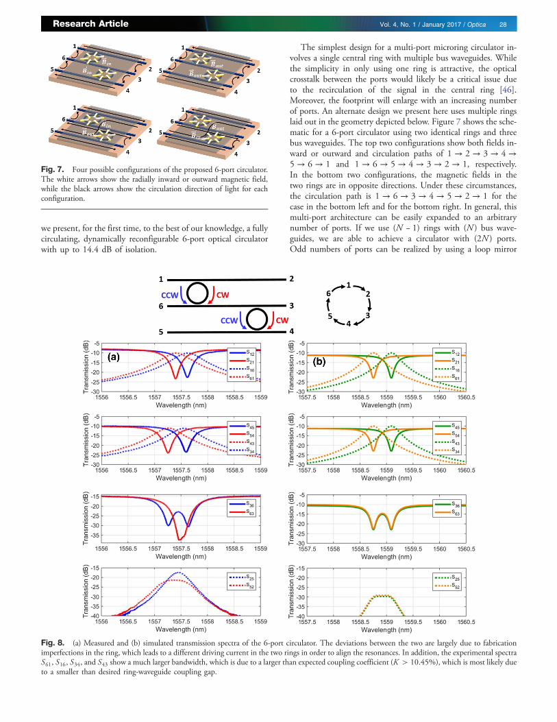
The simplest design for a multi-port microring circulator in-volves a single central ring with multiple bus waveguides. Whilethe simplicity in only using one ring is attractive, the opticalcrosstalk between the ports would likely be a critical issue dueto the recirculation of the signal in the central ring [46].Moreover, the footprint will enlarge with an increasing numberof ports. An alternate design we present here uses multiple ringslaid out in the geometry depicted below. Figure 7 shows the sche-matic for a 6-port circulator using two identical rings and threebus waveguides. The top two configurations show both fields in-ward or outward and circulation paths of 1 → 2 → 3 → 4 →5 → 6 → 1 and 1 → 6 → 5 → 4 → 3 → 2 → 1, respectively.In the bottom two configurations, the magnetic fields in thetwo rings are in opposite directions. Under these circumstances,the circulation path is 1 → 6 → 3 → 4 → 5 → 2 → 1 for thecase in the bottom left and for the bottom right. In general, thismulti-port architecture can be easily expanded to an arbitrarynumber of ports. If we use (N − 1) rings with (N ) bus wave-guides, we are able to achieve a circulator with (2N ) ports.Odd numbers of ports can be realized by using a loop mirror
Fig. 7. Four possible configurations of the proposed 6-port circulator.The white arrows show the radially inward or outward magnetic field,while the black arrows show the circulation direction of light for eachconfiguration.
Fig. 8. (a) Measured and (b) simulated transmission spectra of the 6-port circulator. The deviations between the two are largely due to fabricationimperfections in the ring, which leads to a different driving current in the two rings in order to align the resonances. In addition, the experimental spectraS61, S16, S34, and S43 show a much larger bandwidth, which is due to a larger than expected coupling coefficient (K > 10.45%), which is most likely dueto a smaller than desired ring-waveguide coupling gap.
Research Article Vol. 4, No. 1 / January 2017 / Optica 28
at the end of one of the bus waveguides, as was previouslydemonstrated with a 3-port circulator [32].
As long the rings are separated far enough such that the mag-netic field in one ring does not significantly affect the others, thenwe can magneto-optically tune the (N − 1) rings independentlyand reconfigure the circulator in 2�N − 1� ways. For a 6-port cir-culator, it is possible to obtain the four different configurationsshown above, depending on the orientation of the magnetic fieldin the two rings. We fabricated this 6-port optical circulator usingtwo 20 μm ring resonators and three bus waveguides. In theory,the rings should be identical with the same resonance wavelength,but this is often not the case due to fabrication imperfections andnonuniformities of the wafer or the etch process. Our result showsthe intrinsic resonances of the two rings are over 1 nm apart,meaning they must be thermally tuned together in order forthe circulator to operate at a common wavelength for all ofthe ports. Furthermore, we must apply enough current to observea significant RWS in each of the rings for nonreciprocal behavior.
In this design, the single microstrip can be used to meet bothof the aforementioned requirements for single wavelength circu-lation and compensate for the fabrication. Applying a differentcurrent in each ring, we found that the optimal conditions for6-port circulation in the device under test are I1 � �185 mAfor the top ring and I 2 � �262 mA for the bottom ring.Due to the angling of the output facets and limited spacing be-tween adjacent facets, it was not possible to simultaneously test allinput and output combinations. Instead, we use each of the sixports as an input successively and measure the transmission spec-tra through all the accessible output ports, as shown in Fig. 8.Further details can be found in the Supplement 1.
Although the predicted RWS is 0.35 nm, from the measuredspectra we observe a RWS of 0.25 nm for the top ring while theRWS of the bottom one is 0.35 nm, as shown in Fig. 8. This isreasonable considering the applied current was larger for the bot-tom ring in order to compensate the fabrication variation. In thisconfiguration, the operating wavelength near 1557.6 nm is onresonance with the CCW modes of both rings, causing a circu-lation path of 1 → 2 → 3 → 4 → 5 → 6 → 1. From these mea-surements we can extract the scattering parameters of the device atthe working wavelength in Table 3. Once again, the highlightedentries show the insertion loss along the forward circulation path,and the isolation and crosstalk for each port can be extracted byanalyzing the table. Here, we find the largest isolation ratio is14.4 dB between ports 2 and 3 (i.e., IR23 � jS23j2∕jS32j2), whilethe smallest isolation ratio is 2.5 dB between ports 1 and 6 (i.e.,IR61 � jS16j2∕jS61j2). The insertion losses along the forwardcirculating path range from 10.1 to 14.3 dB, which is similarto what was measured in the 4-port device, and can be reduced
by shortening the length of the Ce:YIG cladding above the buswaveguides. Overall, a better device performance can be achievedby aligning the resonances with better fabrication accuracy or aseparate thermal tuner.
6. CONCLUSIONS
In conclusion, we have demonstrated, for the first time, to thebest of our knowledge, a microring-based optical circulator thatgreatly shrinks the footprint of the device when compared toprevious MZI-based circulators. The device uses an integratedelectromagnet instead of conventional permanent magnets andcan be easily reconfigured to select the direction of circulation,which may lead to new applications in sensing, data centers,and telecommunications. Finally, the device architecture we haveproposed can be scaled to circulators with an arbitrary number ofports and multiple operating configurations. We demonstrate a6-port circulator with up to 14.4 dB of isolation as a proof ofconcept. This scalability combined with a sub-nanosecond swit-ching time could pave the way for novel optical switching androuting technologies.
Funding. Air Force Small Business Innovation Research(SBIR) (FA8650-16-C-1758); National Science Foundation(NSF) (CNS-0960316).
Acknowledgment. The authors also thank Jon Peters,Michael Davenport, and Tin Komljenovic from the Universityof California Santa Barbara, and Fabrizio Di Pasquale fromScuola Sant’Anna of Pisa (Italy) for the insightful advice andhelpful discussions. D.H. also acknowledges the NSF GRFPfor support.
†These authors contributed equally to this work.
See Supplement 1 for supporting content.
REFERENCES
1. D. Jalas, A. Petrov, M. Eich, W. Freude, S. Fan, Z. Yu, R. Baets, M.Popovic, A. Melloni, J. D. Joannopoulos, and M. Vanwolleghem, “Whatis—andwhat is not—an optical isolator,”Nat. Photonics 7, 579–582 (2013).
2. D. Dai and J. E. Bowers, “Silicon-based on-chip multiplexing technolo-gies and devices for Peta-bit optical interconnects,” Nanophotonics 3,283–311 (2014).
3. P. Pintus, N. Andriolli, F. Di Pasquale, and J. E. Bowers, “Bidirectionalcrosstalk and back-reflection free WDM active optical interconnects,”IEEE Photon. Technol. Lett. 25, 1973–1976 (2013).
4. K. Tai, B. Chang, J. Chen, C. H. Mao, T. Ducellier, J. Xie, L. Mao, andJ. Wheeldon, “Wavelength-interleaving bidirectional circulators,” IEEEPhoton. Technol. Lett. 13, 320–322 (2001).
5. H. Krishnaswamy and N. Reikarimian, “Magnetic-free non-reciprocitybased on staggered commutation,” Nat. Commun. 7, 11217 (2016).
6. B. Lee and Y. Jeong, Interrogation Techniques for Fiber Grating Sensorsand the Theory of Fiber Gratings (Marcel Dekker, 2002).
7. H. Lira, Z. Yu, S. Fan, and M. Lipson, “Electrically driven nonreciprocityinduced by interband photonic transition on a silicon chip,” Phys. Rev.Lett. 109, 033901 (2012).
8. Z. Yu and S. Fan, “Complete optical isolation created by indirect inter-band photonic transitions,” Nat. Photonics 3, 91–94 (2009).
9. L. D. Tzuang, K. Fang, P. Nussenzveig, S. Fan, and M. Lipson, “Non-reciprocal phase shift induced by an effective magnetic flux for light,”Nat. Photonics 8, 701–705 (2014).
10. M. J. Heck, S. Srinivasan, M. L. Davenport, and J. E. Bowers, “Integratedmicrowave photonic isolators: theory, experimental realization and appli-
Table 3. Experimental Transmittance Data [dB] of the6-Port Circulator at the Working Wavelength λ � 1557.6 nm
Input Port
Output Port
1 2 3 4 5 61 – −22.5 – – – −10.12 −11.2 – −26.5 – −20.4 –3 – −12.1 – −15.5 – −29.34 – – −11.3 – −23.5 –5 – −23.0 – −12.0 – −27.06 −12.6 – −30.3 – −14.3 –
Research Article Vol. 4, No. 1 / January 2017 / Optica 29

cation in a unidirectional ring mode-locked laser diode,” Photonics 2,957–968 (2015).
11. Y. Yang, C. Galland, Y. Liu, K. Tan, R. Ding, Q. Li, K. Bergman, T. Baehr-Jones, and M. Hochberg, “Experimental demonstration of broadbandLorentz non-reciprocity in an integrable photonic architecture basedon Mach–Zehnder modulators,” Opt. Express 22, 17409–17422 (2014).
12. C. R. Doerr, N. Dupuis, and L. Zhang, “Optical isolator using two tandemphase modulators,” Opt. Lett. 36, 4293–4295 (2011).
13. C. R. Doerr, L. Chen, and D. Vermeulen, “Silicon photonics broadbandmodulation-based isolator,” Opt. Express 22, 4493–4498 (2014).
14. C. G. Poulton, R. Pant, A. Byrnes, S. Fan, M. J. Steel, and B. J. Eggleton,“Design for broadband on-chip isolator using stimulated Brillouin scatter-ing in dispersion-engineered chalcogenide waveguides,” Opt. Express.20, 21235–21246 (2012).
15. C. H. Dong, Z. Shen, C. L. Zou, Y. L. Zhang, W. Fu, and G. C. Guo,“Brillouin-scattering-induced transparency and non-reciprocal lightstorage,” Nat. Commun. 6, 6193 (2015).
16. L. Fan, J.Wang, L. T. Varghese, H. Shen, B. Niu, Y. Xuan, A.M.Weiner, andM. Qi, “An all-silicon passive optical diode,” Science 335, 447–450 (2012).
17. L. Liu, J. Dong, D. Gao, A. Zheng, and X. Zhang, “On-chip passive three-port circuit of all-optical ordered-route transmission,” Sci. Rep. 5, 10190(2015).
18. Y. Shi, Z. Yu, and S. Fan, “Limitations of nonlinear optical isolators due todynamic reciprocity,” Nat. Photonics 9, 388–392 (2015).
19. B. J. Stadler and T. Mizumoto, “Integrated magneto-optical materials andisolators: a review,” IEEE Photon. J. 6, 1–15 (2014).
20. L. Bi, J. Hu, P. Jiang, D. H. Kim, G. F. Dionne, L. C. Kimerling, and C. A.Ross, “On-chip optical isolation in monolithically integrated non-reciprocal optical resonators,” Nat. Photonics 5, 758–762 (2011).
21. X. Y. Sun, Q. Du, T. Goto, M. C. Onbasli, D. H. Kim, N. M. Aimon, J. Hu,and C. A. Ross, “Single-step deposition of cerium-substituted yttrium irongarnet for monolithic on-chip optical isolation,” ACS Photon. 2, 856–863(2015).
22. A. D. Block, P. Dulal, B. J. Stadler, and N. C. Seaton, “Growth param-eters of fully crystallized YIG, Bi:YIG, and Ce:YIG films with high Faradayrotations,” IEEE Photon. J. 6, 1–8 (2014).
23. T. Goto, Y. Eto, K. Kobayashi, Y. Haga, M. Inoue, and C. A. Ross,“Vacuum annealed cerium-substituted yttrium iron garnet films onnon-garnet substrates for integrated optical circuits,” J. Appl. Phys.113, 17A939 (2013).
24. D. Liang, G. Roelkens, R. Baets, and J. E. Bowers, “Hybrid integratedplatforms for silicon photonics,” Materials 3, 1782–1802 (2010).
25. M. J. Heck, J. F. Bauters, M. L. Davenport, J. K. Doylend, S. Jain, G.Kurczveil, S. Srinivasan, Y. Tang, and J. E. Bowers, “Hybrid silicon pho-tonic integrated circuit technology,” IEEE J. Sel. Top. Quantum Electron.19, 6100117 (2013).
26. T. Komljenovic, M. Davenport, J. Hulme, A. Y. Liu, C. T. Santis,A. Spott, S. Srinivasan, E. J. Stanton, C. Zhang, and J. E. Bowers,“Heterogeneous silicon photonic integrated circuits,” J. LightwaveTechnol. 34, 20–35 (2016).
27. Y. Shoji, T. Mizumoto, H. Yokoi, I. W. Hseih, and R. M. Osgood, Jr.,“Magneto-optical isolator with silicon waveguides fabricated by directbonding,” Appl. Phys. Lett. 92, 071117 (2008).
28. Y. Shoji, Y. Shirato, and T. Mizumoto, “Silicon Mach–Zehnder interfer-ometer optical isolator having 8 nm bandwidth for over 20 dB isolation,”J. Appl. Phys. 53, 022202 (2014).
29. Y. Shoji, M. Ito, Y. Shirato, and T. Mizumoto, “MZI optical isolator withSi-wire waveguides by surface-activated direct bonding,” Opt. Express20, 18440–18448 (2012).
30. Y. Shoji, K. Miura, and T. Mizumoto, “Optical nonreciprocal devicesbased on magneto-optical phase shift in silicon photonics,” J. Opt. 18,013001 (2015).
31. K. Mitsuya, Y. Shoji, and T. Mizumoto, “Demonstration of a silicon wave-guide optical circulator,” IEEE Photon. Technol. Lett. 25, 721–723(2013).
32. S. Ghosh, S. Keyvaninia, W. Van Roy, T. Mizumoto, G. Roelkens, and R.Baets, “Adhesively bonded Ce:YIG/SOI integrated optical circulator,”Opt. Lett. 38, 965–967 (2013).
33. S. Ghosh, S. Keyvaninia, Y. Shirato, T. Mizumoto, G. Roelkens, and R.Baets, “Optical isolator for TE polarized light realized by adhesive bond-ing of Ce:YIG on silicon-on-insulator waveguide circuits,” IEEE Photon.J. 5, 6601108 (2013).
34. M. C. Tien, T. Mizumoto, P. Pintus, H. Kroemer, and J. E. Bowers,“Silicon ring isolators with bonded nonreciprocal magneto-optic garnets,”Opt. Express 19, 11740–11745 (2011).
35. P. Pintus, F. Di Pasquale, and J. E. Bowers, “Integrated TE and TM op-tical circulators on ultra-low-loss silicon nitride platform,” Opt. Express21, 5041–5052 (2013).
36. M. Yanaga, Y. Shoji, Y. Takamura, S. Nakagawa, and T. Mizumoto,“Compact magnetooptical isolator with cobalt ferrite on silicon photoniccircuits,” Appl. Phys. Express 8, 082201 (2015).
37. D. Huang, P. Pintus, C. Zhong, Y. Shoji, T. Mizumoto, and J. E. Bowers,“Silicon microring isolator with large optical isolation and low loss,” inOptical Fiber Communication Conference (Optical Society of America,2016), paper Th1K-2.
38. D. Huang, P. Pintus, C. Zhong, Y. Shoji, T. Mizumoto, and J. E. Bowers,“Electrically driven and thermally tunable integrated optical isolators forsilicon photonics,” IEEE J. Sel. Top. Quantum Electron. 22, 4403408(2016).
39. M. Levy, R. M. Osgood, H. Hegde, F. J. Cadieu, R. Wolfe, and V. J.Fratello, “Integrated optical isolators with sputter-deposited thin-filmmagnets,” IEEE Photon. Technol. Lett. 8, 903–905 (1996).
40. P. Pintus, M. C. Tien, and J. E. Bowers, “Design of magneto-optical ringisolator on SOI based on the finite-element method,” IEEE Photon.Technol. Lett. 23, 1670–1672 (2011).
41. P. Pintus, “Accurate vectorial finite element mode solver for magneto-optic and anisotropic waveguides,” Opt. Express 22, 15737–15756(2014).
42. K. Furuya, T. Nemoto, K. Kato, Y. Shoji, and T. Mizumoto, “Athermaloperation of a waveguide optical isolator based on canceling phase de-viations in a Mach–Zehnder interferometer,” J. Lightwave Technol. 34,1699–1705 (2016).
43. P. Pintus, D. Huang, C. Zhang, Y. Shoji, T. Mizumoto, and J. E. Bowers,“Novel nonreciprocal devices with integrated electromagnet for siliconphotonics,” in European Conference on Optical Communication (2016).
44. K. Padmaraji and K. Bergman, “Resolving the thermal challengesfor silicon microring resonator devices,” Nanophotonics 3, 269–281(2014).
45. I. Tudosa, C. Stamm, A. B. Kashuba, F. King, H. C. Siegmann, J. Stöhr,G. Ju, B. Lu, and D. Weller, “The ultimate speed of magnetic switching ingranular recording media,” Nature 428, 831–833 (2004).
46. P. Pintus, P. Contu, P. G. Raponi, I. Cerutti, and N. Andriolli, “Silicon-based all-optical multi microring network-on-chip,” Opt. Lett. 39,797–800 (2014).
Research Article Vol. 4, No. 1 / January 2017 / Optica 30


![A Dynamically Reconfigurable ECG Analog Front-End with a 2.5 …bioee.ucsd.edu/papers/A Dynamically Reconfigurable ECG... · 2017-06-01 · State-of-the-art low power ECG AFEs [1-2]](https://static.fdocuments.us/doc/165x107/5f13579cde6f341989253c27/a-dynamically-reconfigurable-ecg-analog-front-end-with-a-25-bioeeucsdedupapersa.jpg)