Dynamic Synchronizer Flip-Flop Performance in … · The Dynamic Latch Flip-Flop performed the best...
7
Dynamic Synchronizer Flip-Flop Performance in FinFET Technologies Mark Buckler‡*, Arpan Vaidya†, Xiaobin Liu†, and Wayne Burleson†‡ †University of Massachusetts, Amherst, MA, USA ‡AMD Research, Boxborough, MA, USA *Cornell University, Ithaca, NY, USA [email protected], {avaidya, and xlu}@umass.edu Abstract—The use of fine-grain Dynamic Voltage and Fre- quency Scaling (DVFS) has increased the number of distinct clock domains on a given Network-on-Chip (NoC). This necessitates robust synchronizers to prevent clock domain communication failures, even as FinFET devices have begun to replace planar devices. This paper presents simulation results and comparisons between dynamic (requiring reset) and non-dynamic synchronizer flip-flops implemented in predictive models for both planar tech- nologies and future FinFET technologies. Results demonstrate that synchronizers built with FinFET devices 1) exhibit a tau value which continues to scale with fan-out of four delay and 2) can be improved with forward biasing, but 3) are more sensitive to temperature. Dynamic flip-flops settled metastability fastest when using standard technology voltages, but previously couldn’t be used in non-dynamic systems. For this reason, a new synchronizer design is also presented which exploits the benefits of dynamic flip-flops without the need for a dedicated reset signal. Keywords—NoC, GALS, Synchronizers, Metastability, FinFET I. I NTRODUCTION Both the increase in the number of independent cores per system, and the use of fine grained Dynamic Voltage and Frequency Scaling (DVFS), has led to an increase in the number of clock domains per Network-on-Chip (NoC). Communication across these clock domains often requires the use of ”brute force” synchronizers which rely on highly opti- mized synchronizer flip-flops connected in series. As CMOS continues to scale, circuit designers must re-evaluate design trade-offs for each new technology node. Now that semi- conductor manufacturers are moving from planar CMOS to FinFET CMOS, circuit designers must prepare for changes of an even larger scale. Previous work has focused on the effect of technology scaling on synchronizers in planar technology [1]–[5], but this paper aims to demonstrate the effects of FinFET de- vices. To evaluate their effects, HSPICE simulations using predictive technology models developed at ASU [6] were performed and compared with theoretical analysis. While on- chip synchronizer evaluation techniques have been developed [7], building test chips for multiple technology nodes would be both prohibitively expensive and impossible for nodes not yet in production (such as 10nm and 7nm). This paper’s key contributions include simulation results and theoretical analysis on three high performance synchronizer flip-flops in five different technology nodes. The simulation results presented in this paper demonstrate the continual relationship between tau (τ ) and fan-out of four (FO4) delay even in FinFET devices. It was also found that body biasing synchronizer feedback loops is still effective in FinFET devices, but not as significant as with planar devices. FinFET synchronizers were also observed to be more sensitive to temperature variations. The Dynamic Latch Flip-Flop performed the best at standard voltage levels. For this reason, this paper also presents The Dynamic Synchronizer, which enables the use of dynamic synchronizing flip-flops in non-dynamic systems. II. BACKGROUND When communicating across clock domains the transmitted data and receiving clock are not aligned. Therefore setup and hold times are likely to be violated, possibly causing metastability. Metastability occurs when the bi-stable element within the flip-flop does not have enough time to fully charge or discharge, resulting in a half-charged element. This half- charge is usually very close to ( V DD 2 ), and is not logic high or logic low. The element will eventually settle, but it is impossible to predict when the settling will occur or which state it will settle to. Brute force synchronizers are designed as a chain of flip-flops connected in series, and reduce the possibility of metastability entering the receive domain’s logic. Each additional flip-flop reduces the possibility of metastabil- ity, but the synchronizer will always retain a finite chance of failure (metastability manifesting on the output). Since additional flip-flops also result in an increased latency through the synchronizer, a trade-off between latency and reliability exists. To quantify the frequency of these failures, brute force synchronizer reliability is commonly expressed as the Mean Time Between Failures (MTBF). The expression in Equation (1) shows dependence on the receiver clock frequency (F C ) and incoming data frequency (F D ). These factors are inde- pendent of the flip-flops within the synchronizer, and so these factors are assumed to not change with technology scaling. The factor S is defined as the settling time, and is often simplified as the receiver clock period multiplied by the number of flip- flop stages. This is generally a design parameter which can be varied to achieve the desired MTBF. Since this factor is not dependent on the properties of the individual flip-flops, it is unaffected by process technology. MTBF = e S τ T W F C F D (1) 978-1-4799-5347-9/14/$31.00 ©2014 IEEE 2014 Eighth IEEE/ACM International Symposium on Networks-on-Chip (NoCS) 104
-
Upload
trannguyet -
Category
Documents
-
view
233 -
download
0
Transcript of Dynamic Synchronizer Flip-Flop Performance in … · The Dynamic Latch Flip-Flop performed the best...

Dynamic Synchronizer Flip-Flop Performance inFinFET Technologies
Mark Buckler‡∗, Arpan Vaidya†, Xiaobin Liu†, and Wayne Burleson†‡†University of Massachusetts, Amherst, MA, USA‡AMD Research, Boxborough, MA, USA∗Cornell University, Ithaca, NY, USA
[email protected], {avaidya, and xlu}@umass.edu
Abstract—The use of fine-grain Dynamic Voltage and Fre-quency Scaling (DVFS) has increased the number of distinct clockdomains on a given Network-on-Chip (NoC). This necessitatesrobust synchronizers to prevent clock domain communicationfailures, even as FinFET devices have begun to replace planardevices. This paper presents simulation results and comparisonsbetween dynamic (requiring reset) and non-dynamic synchronizerflip-flops implemented in predictive models for both planar tech-nologies and future FinFET technologies. Results demonstratethat synchronizers built with FinFET devices 1) exhibit a tauvalue which continues to scale with fan-out of four delay and 2)can be improved with forward biasing, but 3) are more sensitive totemperature. Dynamic flip-flops settled metastability fastest whenusing standard technology voltages, but previously couldn’t beused in non-dynamic systems. For this reason, a new synchronizerdesign is also presented which exploits the benefits of dynamicflip-flops without the need for a dedicated reset signal.
Keywords—NoC, GALS, Synchronizers, Metastability, FinFET
I. INTRODUCTION
Both the increase in the number of independent coresper system, and the use of fine grained Dynamic Voltageand Frequency Scaling (DVFS), has led to an increase inthe number of clock domains per Network-on-Chip (NoC).Communication across these clock domains often requires theuse of ”brute force” synchronizers which rely on highly opti-mized synchronizer flip-flops connected in series. As CMOScontinues to scale, circuit designers must re-evaluate designtrade-offs for each new technology node. Now that semi-conductor manufacturers are moving from planar CMOS toFinFET CMOS, circuit designers must prepare for changes ofan even larger scale.
Previous work has focused on the effect of technologyscaling on synchronizers in planar technology [1]–[5], butthis paper aims to demonstrate the effects of FinFET de-vices. To evaluate their effects, HSPICE simulations usingpredictive technology models developed at ASU [6] wereperformed and compared with theoretical analysis. While on-chip synchronizer evaluation techniques have been developed[7], building test chips for multiple technology nodes wouldbe both prohibitively expensive and impossible for nodes notyet in production (such as 10nm and 7nm). This paper’s keycontributions include simulation results and theoretical analysison three high performance synchronizer flip-flops in fivedifferent technology nodes. The simulation results presentedin this paper demonstrate the continual relationship between
tau (τ ) and fan-out of four (FO4) delay even in FinFETdevices. It was also found that body biasing synchronizerfeedback loops is still effective in FinFET devices, but not assignificant as with planar devices. FinFET synchronizers werealso observed to be more sensitive to temperature variations.The Dynamic Latch Flip-Flop performed the best at standardvoltage levels. For this reason, this paper also presents TheDynamic Synchronizer, which enables the use of dynamicsynchronizing flip-flops in non-dynamic systems.
II. BACKGROUND
When communicating across clock domains the transmitteddata and receiving clock are not aligned. Therefore setupand hold times are likely to be violated, possibly causingmetastability. Metastability occurs when the bi-stable elementwithin the flip-flop does not have enough time to fully chargeor discharge, resulting in a half-charged element. This half-charge is usually very close to (VDD2 ), and is not logic highor logic low. The element will eventually settle, but it isimpossible to predict when the settling will occur or whichstate it will settle to. Brute force synchronizers are designedas a chain of flip-flops connected in series, and reduce thepossibility of metastability entering the receive domain’s logic.Each additional flip-flop reduces the possibility of metastabil-ity, but the synchronizer will always retain a finite chanceof failure (metastability manifesting on the output). Sinceadditional flip-flops also result in an increased latency throughthe synchronizer, a trade-off between latency and reliabilityexists. To quantify the frequency of these failures, brute forcesynchronizer reliability is commonly expressed as the MeanTime Between Failures (MTBF). The expression in Equation(1) shows dependence on the receiver clock frequency (FC)and incoming data frequency (FD). These factors are inde-pendent of the flip-flops within the synchronizer, and so thesefactors are assumed to not change with technology scaling. Thefactor S is defined as the settling time, and is often simplifiedas the receiver clock period multiplied by the number of flip-flop stages. This is generally a design parameter which can bevaried to achieve the desired MTBF. Since this factor is notdependent on the properties of the individual flip-flops, it isunaffected by process technology.
MTBF =eSτ
TWFCFD(1)
978-1-4799-5347-9/14/$31.00 ©2014 IEEE
2014 Eighth IEEE/ACM International Symposium on Networks-on-Chip (NoCS)
104

TW (the sensitive region) and τ (evaluation time constant)are both dependent on the individual flip-flop however, and aretherefore affected by changes in process technology. Althoughsome papers have considered the effects of TW [7], TW onlyaffects MTBF linearly while τ is exponential. For this reason,much of the past work has chosen to focus on τ rather thanTW [8], [9]. More complex expressions have been proposed foraccurately calculating the MTBF of multi-stage synchronizers;but these expressions still show that τ is the most dominantfactor [10].
The value of τ can be affected by many environmentalfactors, but circuit structure plays a central role. Two circuitparameters of particular importance are transistor strength andnode capacitance. A number of circuit topologies have beendesigned to minimize the necessary node capacitance, whilealso improving the gain of the flip-flop feedback loop [2], [9],[11]–[14]. Device sizing is also important, and so a multitudeof techniques have been proposed to effectively manage thetradeoff between device strength and size [2], [13], [15]. Sometechniques have also considered adding supplementary devicesbut these studies have had mixed results [14], [16].
Naturally, both transistor strength and node capacitancechange as technology scales. One key parameter used tocompare technology nodes is the fan out of four delay (com-monly referred to as FO4). Since the early days of CMOS,designers have tracked both FO4 and τ , finding them to scaletogether [1]. As planar technology has continue to scale, someresearchers claim that this trend has continued [2], [3] whileothers claim that after 65nm this is no longer the case [4],[5]. In this paper we demonstrate through theoretical analysisand simulation results that FO4 and τ , do continue to scaletogether both in planar and in FinFET technology.
FinFET devices offer a number of significant benefits inaddition to allowing the continuation of Moore’s Law. Twoof the most well-known benefits of FinFET technology aredecreased leakage current and less variation in V t betweenprocess corners [17], [18]. All circuits will benefit from adecrease in leakage current, including synchronizers. Leakageis not a dominant effect on synchronizer performance however,and so this particular improvement is not considered in thiswork. The effect of tighter process corners will also havean impact of synchronizers since they must be designed forthe worst case. The end result of this is expected to be anoverall improvement in synchronizer performance, but wouldnot affect design trade-offs. Process corners are also heavilydefined by laboratory experimentation, and therefore futuretechnology simulation models do not consider them [6].
III. EXPERIMENTAL METHODOLOGY
A. Simulating τ
The HSPICE simulation strategy used to generate theresults found in this paper was modeled on a hardware testingmethodology developed by Dike and Burton [9]. A similarsimulation based adaption of this technique has recently beenused in other synchronizer design research [8]. In the originalhardware technique, memory cell nodes are first forced intometastable levels. For simulation, this is accomplished with ini-tial conditions. Once forced into metastability, measurementsare taken as the circuit begins to self-correct back to a stable
Fig. 1: Synchronizer Bi-stable Element Circuit Response
value (a logical high or low value). The speed at which thecircuit can self-correct is recorded, and used to calculate thevalue of τ . This gives an accurate value without needing torely on simulation methods which require data vs. clock timesweeps. Data vs. clock time sweep τ simulation methods haveproven to be unreasonable given HSPICE’s sensitivity [9].
Bi-stable devices within synchronizer flip-flops generallyhave two sides. This is most easily understood when consid-ering an inverter loop. When stable, the voltage of one side ofthe loop is at VDD while the other is GND. When both sidesare forced to be VDD
2 , the voltage difference between the twonodes is zero. As the bi-stable element begins to settle, thisvoltage difference begins to increase or decrease depending onthe polarity. Fig.1 shows how this occurs in simulation. Theproperties of this change are used to calculate τ , as shown inequation (2). Two points which represent the linear section inFig. 1 are selected, and these two points are entered into theformula as (t1,V1) and (t2,V2).
τ =t1 − t2
ln(V2/V1)(2)
B. Flip-flop Initialization
As described, the first step in simulation is forcing the flip-flop under test into metastability. This paper considers threesynchronizer flip-flops which each utilize different bi-stableelement structures. Each bi-stable element structure requires adifferent method of initialization.
The first flip-flop considered was the Dynamic Latch Flip-Flop (DLFF), sometimes referred to as a jamb latch flip-flop[9]. The DLFF is so named due to the dynamic nature of itscircuit, which requires a separate reset signal before the devicecan be re-evaluated (refer to Fig. 3). This modification reducesthe capacitance on the element, which enables the circuit tooutperform standard synchronizer flip-flops. Unfortunately italso limits the usabililty of the circuit in modern deviceswhich very rarely contain a dynamic reset signal. Since theDLFF utilizes a simple cross-coupled inverter pair, initializingthe circuit into metastability is similar to what has been justdescribed.
2014 Eighth IEEE/ACM International Symposium on Networks-on-Chip (NoCS)
105

The second circuit simulated was the PowerPC flip-flop,recently considered as a suitable sub-threshold voltage syn-chronizer flip-flop [11]. The PowerPC flip-flop as shown inFig.4, was initialized by setting the pass gate transistor switchand all Wp2 and Wn2 devices in the ON state. The data inputis then set to VDD
2 . The voltage difference is then consideredbetween node X and output of the inverter consisting of Wp1and Wn1.
The Pseudo-NMOS flip-flop is the third to be simulated,and is shown in Fig.5. This flip-flop was initially proposed asa bi-stable element which did not sharply degrade in speed asVDD was reduced. To initialize the Pseudo-NMOS flip-flop,the q and q nodes were set at VDD
2 , and then the clock wasset to low such that that mm and mm were in the same state.The voltage difference was taken between q and q.
IV. RESULTS
A. τ and FO4 delay
The link between synchronizer flip-flop τ values and FO4delay has been used in the past to predict synchronizer τ innew technologies. Both factors rely on the device size/strengthtradeoff defined by the technology node. However, the researchcommunity has disagreed about whether or not this trendcontinues [1]–[5]. Ginosar et al. have proposed that after 65nm,each technology node will see higher τ while FO4 delaywill continue to decrease [4]. They justify this claim by firstcreating a mathematical relationship between FO4 delay andτ in (3).
τ =η
4
td,FO4
A(3)
Equation 3 represents τ as a function of FO4 delay, A(inverter gain), and η (derived from a combination of VDD,Vt, and λ). It was proposed that while FO4 will continue toscale, the inverter gain will not, creating a degradation in τ[4]. Other researchers have released results demonstrating τvalues which continue to track FO4 delay [2]. Until now, the
Fig. 2: τFO4 For Planar and FinFET Nodes
Fig. 3: Dynamic Latch Flip-Flop [9]
Fig. 4: PowerPC Flip-Flop [11]
Fig. 5: Pseudo-NMOS Flip-Flop [2]
2014 Eighth IEEE/ACM International Symposium on Networks-on-Chip (NoCS)
106

(a) 22nm Planar (b) 20nm FinFET
Fig. 6: DLFF τ with Temperature and VDD sweep
(a) 22nm Planar (b) 20nm FinFET
Fig. 7: Pseudo-NMOS τ with Temperature and VDD sweep
effect of FinFET devices has not yet been considered. Analysisfrom UC Berkeley has found that propagation delay in FinFETcircuits is independent of electrical width [19]. This serves tomaintain the gain of inverter built with FinFET devices, evenas they are scaled. The factor of consideration relating τ andFO4 delay is inverter gain, and so it stands to reason that τwill continue to track FO4 delay even when using FinFETs.
This analysis is validated by the simulation results shown inFig.2. Each of the three synchronizer flip-flops were simulatedwith a nominal VDD of 0.7V and temperature of 22◦C. Theexpected range for τ delay is between 0.2 and 1.5 times thegiven technology node’s FO4 delay [4], and each of the threeflip-flops tested fall within this range. While there is somevariation between technology nodes, the results still matchphysically measured results by other researchers for planartechnology nodes [2]. The FinFET nodes (7nm, 10nm, and20nm) stay within the same τ
FO4 range as the values foundfor planar nodes (22nm, 50nm).
B. τ and Temperature
As the temperature of a CMOS circuit increases, the carriermobility is reduced (due to an increase in particle scattering)and the threshold voltage decreases. While these effects haveopposite effects on CMOS speed, the decrease in mobility ismore dominant for most circuits (higher temperatures mean
slower logic) [20]. However, previous work has verified thatthe threshold voltage’s temperature sensitivity is more impor-tant than mobility’s sensitivity for synchronizer circuits, result-ing in an increase in synchronizer τ with lower temperatures[7], [21]. FinFET devices are not affected by temperature inthe same way as planar devices however. Recent work hasfound that the previously weaker voltage threshold effect isactually dominant in FinFET logic gates, which has led toan increase in logic gate performance at higher temperatures[22]. Unfortunately, this suggests a sharp increase in τ at lowertemperatures for synchronizers built with FinFET devices.
The simulation results, shown in Fig. 6 and Fig. 7, dovalidate the theory predicting significantly higher τ values forFinFETs at low temperatures. While simulation was completedfor all nodes mentioned before, 22nm planar and 20nm FinFETare shown here due to their similar physical dimensions. Thereis a more stark degredation (increase) of synchronizer τ atlower temperatures for circuits built with FinFET devices(7nm and 20nm). When built with planar devices in 22nmand 50nm technology, the DLFF and Pseudo-NMOS flip-flop are generally stable over temperature, even with lowsupply voltages. Therefore a general increase in temperaturedependence with scaling can also be observed. The PowerPCflip-flop experienced these same effects, but its associated datais not displayed here in order to conserve space.
2014 Eighth IEEE/ACM International Symposium on Networks-on-Chip (NoCS)
107

(a) 22nm Planar (b) 20nm FinFET
Fig. 8: DLFF and Pseudo-NMOS τ when Non-Biased or Forward-Biased with VDD sweep
These results also show that increases in τ due to lowertemperatures can be prevented with a higher supply voltage.This further demonstrates that the dominant factor in synchro-nizer dependence on temperature is the change in thresholdvoltage. In modern SoCs, maximum restrictions on the supplyvoltage are generally enforced to prevent an increase in powerconsumption which leads to heat. Fortunately, this means thatraising the supply voltage in a low temperature state to preventτ degradation is not unreasonable.
C. Forward Biasing
Designers must also consider how FinFET devices willaffect the trade-offs between various synchronizing flip-floptypes. When all circuits were implemented with FinFET de-vices, the Power-PC flip-flop continued to be out-performedby both the DLFF and Pseudo-NMOS. However, the choicebetween the DLFF and Pseudo-NMOS becomes more complexwhen FinFET devices are used.
The DLFF was one of the first synchronizing flip-flopsto be proposed, and relies on inverter feedback loops to settlemetastability [9]. When near-threshold operation became morecommon, it was shown that inverter loops provided very poorτ at low voltages. For this reason, the Pseudo-NMOS flip-flop was proposed as a synchronizing flip-flop without theneed for an inverter feedback loop [2]. Around the same time,another solution was proposed. This solution applied forwardbody bias to increase DLFF performance at low voltages [8].It was demonstrated that forward body biasing increases thetransconductance of the bi-stable inverter pair, resulting in adecrease in τ . While the Pseudo-NMOS has been comparedto the unbiased DLFF, it has not yet been compared whenusing this technique. It is important to determine which designoutperforms the other at low voltages, as well as verificationof the technique’s effectiveness when using FinFET devices.
For 22nm planar technology, Fig.8(a) shows that the non-
biased DLFF has the worst τ . However, when forward bodybiasing is applied the DLFF τ is significantly decreased. Iteven surpasses the biased Pseudo-NMOS flip-flop, which isrelatively unchanged. This demonstrates that forward biasinga planar DLFF is the best solution for both high and near-threshold voltage operation.
In FinFET technology, not only are all τ values signif-icantly reduced (observe the scale in Fig.8(b) vs Fig.8(a)),the tradeoffs change. Since FinFET devices sit on top of thebulk, rather than being deposited inside the bulk (as in planartechnologies), the effect changes. As can be seen in Fig.8(b),both the DLFF and Pseudo-NMOS receive an increase in τrather than a decrease in τ when forward biasing is appliedat low voltages. This effectively removes biasing as a suitabletechnique for near threshold operation.
It can also be seen however that DLFF maintains a sig-nificant advantage over the Pseudo-NMOS at higher supplyvoltages, and can still be improved with forward body biasing.This presents a switching point (around 0.43V for 20nm)when above that voltage the DLFF is superior, and below thatvoltage the Pseudo-NMOS is superior. This is because inverterfeedback loops offer a significant advantage at higher voltages.If the supply voltage must decrease, this advantage wears offand the Pseudo-NMOS achieves the lowest τ for near thresholdoperation.
V. THE DYNAMIC SYNCHRONIZER
Comparing the raw τ values of synchronizer flip-flops isimportant, but not the whole story. There are some limitationswhen these designs are used in real SoCs. While this workhas found the DLFF to outperform the PowerPC and Pseudo-NMOS flip-flops when operated with a higher supply voltage,it requires a separate reset signal. Modern SoCs do not usereset, and so the use of this flip-flop has been limited. This
2014 Eighth IEEE/ACM International Symposium on Networks-on-Chip (NoCS)
108

(a) Schematic (b) Timing Diagram
Fig. 9: Simple Dynamic Synchronizer
paper presents a new circuit which automatically generates therequired reset signal: The Dynamic Synchronizer.
A simple version of the Dynamic Synchronizer is shownin Fig. 9(a), consisting of a single DLFF to sample data andresolve metastability. A normal D flip-flop is used to samplethe output of the DLFF so that the output of the system isno longer affected by the periodic resets experienced by theDLFF. The output of this flip-flop is updated three-quarters ofthe way through the clock cycle.
The behavior of this circuit is described in more detailin Fig. 9(b). In timing event 1, a rising edge on Rclk causesDLFF1 to correctly sample a high value. Then, three-quartersof the way through the clock cycle, a rising edge on theDelayed, inverted, rclk, causes both the Reset of the DLFF1(via a pulse shown in event 2) and the D flip-flop to samplethe output of the DLFF1. While resetting and sampling theoutput of a DLFF at the same time might seem like it violatestiming conditions, this is not the case and has been verified inboth schematic and layout level simulations. This is similar tohow each flip-flop in a brute-force synchronizer samples theflip-flop ahead of it, which is also sampling at that same time[23]. The data on the D flip-flop is now aligned and can besampled by the receive clock domain on the next rising edgeof Rclk.
Although the support structure around the DLFF has nearlyhidden the dynamic behavior of this synchronizer, there isstill one more eccentricity in the circuit’s behavior. For onespecific input combination, the Simple Dynamic Synchronizerwill not sample the input properly. The situation in question iswhen Tdata experiences a falling edge in-between the falling
edge of Reset and rising edge of Rclk. The circuit fails in thiscase because this input combination violates the monotonicityinput restriction required of all dynamic circuits. The SimpleDynamic Synchronizer needs the Reset signal on the first flip-flop to pull its output down. If Reset is not asserted whilethe data experiences a falling edge, the synchronizer will keepsampling a high value until the reset can be reasserted.
The goal is to use this synchronizer in non-dynamic sys-tems which do not maintain monotonic signals, so monotonicinput cannot be assumed. In the case shown in Fig. 9(b) circledin red, Tdata experiences a falling edge in-between the fallingedge of Reset and rising edge of Rclk. This is the specificsituation which causes a problem. Since the DLFF circuit hasno pull up transistors on its data input (see Fig. 3), the outputof the inverter pair can only be truly pulled low with a Resetsignal. In this case the falling edge on the data occurred afterthe reset, so the latches inside the DLFF remained in theirhigh state. This can be observed at timing event 3, where theDLFF1 output incorrectly samples a logic high. This is thensampled by the conventional flip-flop, and the Aligned dataincorrectly displays another high value. The output of DLFF1is finally pulled low when the next Reset pulse occurs (timingevent 4), and on the next rising edge of the Rclk the real datavalue will be seen.
This problem can be solved with a more robust designshown in Fig. 10(a). Since the problem is caused by a fallingedge on Tdata between the falling edge of the Reset and therising edge of Rclk, it is known that the false value caused willalways be a false high value. For this reason, an AND gatehas been inserted in between DLFF1 and the conventional flip-flop. This gates the output of DLFF1 and allows for a detection
(a) Schematic (b) Timing Diagram
Fig. 10: Robust Dynamic Synchronizer
2014 Eighth IEEE/ACM International Symposium on Networks-on-Chip (NoCS)
109
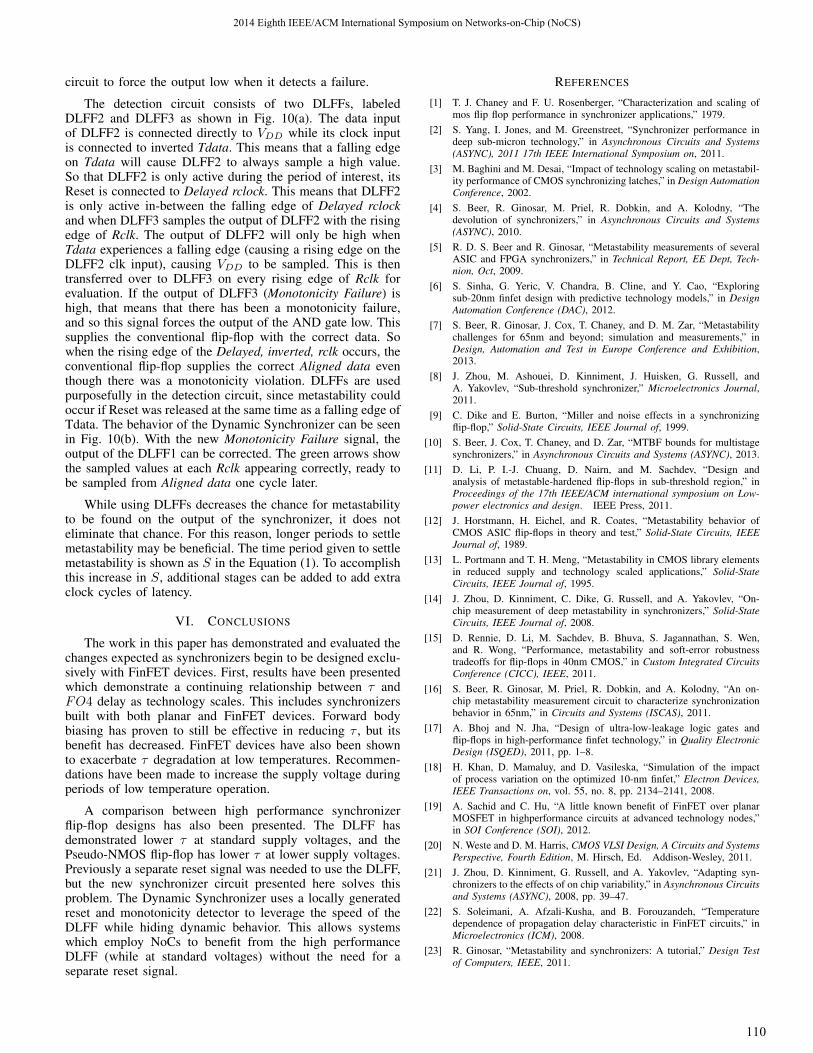
circuit to force the output low when it detects a failure.
The detection circuit consists of two DLFFs, labeledDLFF2 and DLFF3 as shown in Fig. 10(a). The data inputof DLFF2 is connected directly to VDD while its clock inputis connected to inverted Tdata. This means that a falling edgeon Tdata will cause DLFF2 to always sample a high value.So that DLFF2 is only active during the period of interest, itsReset is connected to Delayed rclock. This means that DLFF2is only active in-between the falling edge of Delayed rclockand when DLFF3 samples the output of DLFF2 with the risingedge of Rclk. The output of DLFF2 will only be high whenTdata experiences a falling edge (causing a rising edge on theDLFF2 clk input), causing VDD to be sampled. This is thentransferred over to DLFF3 on every rising edge of Rclk forevaluation. If the output of DLFF3 (Monotonicity Failure) ishigh, that means that there has been a monotonicity failure,and so this signal forces the output of the AND gate low. Thissupplies the conventional flip-flop with the correct data. Sowhen the rising edge of the Delayed, inverted, rclk occurs, theconventional flip-flop supplies the correct Aligned data eventhough there was a monotonicity violation. DLFFs are usedpurposefully in the detection circuit, since metastability couldoccur if Reset was released at the same time as a falling edge ofTdata. The behavior of the Dynamic Synchronizer can be seenin Fig. 10(b). With the new Monotonicity Failure signal, theoutput of the DLFF1 can be corrected. The green arrows showthe sampled values at each Rclk appearing correctly, ready tobe sampled from Aligned data one cycle later.
While using DLFFs decreases the chance for metastabilityto be found on the output of the synchronizer, it does noteliminate that chance. For this reason, longer periods to settlemetastability may be beneficial. The time period given to settlemetastability is shown as S in the Equation (1). To accomplishthis increase in S, additional stages can be added to add extraclock cycles of latency.
VI. CONCLUSIONS
The work in this paper has demonstrated and evaluated thechanges expected as synchronizers begin to be designed exclu-sively with FinFET devices. First, results have been presentedwhich demonstrate a continuing relationship between τ andFO4 delay as technology scales. This includes synchronizersbuilt with both planar and FinFET devices. Forward bodybiasing has proven to still be effective in reducing τ , but itsbenefit has decreased. FinFET devices have also been shownto exacerbate τ degradation at low temperatures. Recommen-dations have been made to increase the supply voltage duringperiods of low temperature operation.
A comparison between high performance synchronizerflip-flop designs has also been presented. The DLFF hasdemonstrated lower τ at standard supply voltages, and thePseudo-NMOS flip-flop has lower τ at lower supply voltages.Previously a separate reset signal was needed to use the DLFF,but the new synchronizer circuit presented here solves thisproblem. The Dynamic Synchronizer uses a locally generatedreset and monotonicity detector to leverage the speed of theDLFF while hiding dynamic behavior. This allows systemswhich employ NoCs to benefit from the high performanceDLFF (while at standard voltages) without the need for aseparate reset signal.
REFERENCES
[1] T. J. Chaney and F. U. Rosenberger, “Characterization and scaling ofmos flip flop performance in synchronizer applications,” 1979.
[2] S. Yang, I. Jones, and M. Greenstreet, “Synchronizer performance indeep sub-micron technology,” in Asynchronous Circuits and Systems(ASYNC), 2011 17th IEEE International Symposium on, 2011.
[3] M. Baghini and M. Desai, “Impact of technology scaling on metastabil-ity performance of CMOS synchronizing latches,” in Design AutomationConference, 2002.
[4] S. Beer, R. Ginosar, M. Priel, R. Dobkin, and A. Kolodny, “Thedevolution of synchronizers,” in Asynchronous Circuits and Systems(ASYNC), 2010.
[5] R. D. S. Beer and R. Ginosar, “Metastability measurements of severalASIC and FPGA synchronizers,” in Technical Report, EE Dept, Tech-nion, Oct, 2009.
[6] S. Sinha, G. Yeric, V. Chandra, B. Cline, and Y. Cao, “Exploringsub-20nm finfet design with predictive technology models,” in DesignAutomation Conference (DAC), 2012.
[7] S. Beer, R. Ginosar, J. Cox, T. Chaney, and D. M. Zar, “Metastabilitychallenges for 65nm and beyond; simulation and measurements,” inDesign, Automation and Test in Europe Conference and Exhibition,2013.
[8] J. Zhou, M. Ashouei, D. Kinniment, J. Huisken, G. Russell, andA. Yakovlev, “Sub-threshold synchronizer,” Microelectronics Journal,2011.
[9] C. Dike and E. Burton, “Miller and noise effects in a synchronizingflip-flop,” Solid-State Circuits, IEEE Journal of, 1999.
[10] S. Beer, J. Cox, T. Chaney, and D. Zar, “MTBF bounds for multistagesynchronizers,” in Asynchronous Circuits and Systems (ASYNC), 2013.
[11] D. Li, P. I.-J. Chuang, D. Nairn, and M. Sachdev, “Design andanalysis of metastable-hardened flip-flops in sub-threshold region,” inProceedings of the 17th IEEE/ACM international symposium on Low-power electronics and design. IEEE Press, 2011.
[12] J. Horstmann, H. Eichel, and R. Coates, “Metastability behavior ofCMOS ASIC flip-flops in theory and test,” Solid-State Circuits, IEEEJournal of, 1989.
[13] L. Portmann and T. H. Meng, “Metastability in CMOS library elementsin reduced supply and technology scaled applications,” Solid-StateCircuits, IEEE Journal of, 1995.
[14] J. Zhou, D. Kinniment, C. Dike, G. Russell, and A. Yakovlev, “On-chip measurement of deep metastability in synchronizers,” Solid-StateCircuits, IEEE Journal of, 2008.
[15] D. Rennie, D. Li, M. Sachdev, B. Bhuva, S. Jagannathan, S. Wen,and R. Wong, “Performance, metastability and soft-error robustnesstradeoffs for flip-flops in 40nm CMOS,” in Custom Integrated CircuitsConference (CICC), IEEE, 2011.
[16] S. Beer, R. Ginosar, M. Priel, R. Dobkin, and A. Kolodny, “An on-chip metastability measurement circuit to characterize synchronizationbehavior in 65nm,” in Circuits and Systems (ISCAS), 2011.
[17] A. Bhoj and N. Jha, “Design of ultra-low-leakage logic gates andflip-flops in high-performance finfet technology,” in Quality ElectronicDesign (ISQED), 2011, pp. 1–8.
[18] H. Khan, D. Mamaluy, and D. Vasileska, “Simulation of the impactof process variation on the optimized 10-nm finfet,” Electron Devices,IEEE Transactions on, vol. 55, no. 8, pp. 2134–2141, 2008.
[19] A. Sachid and C. Hu, “A little known benefit of FinFET over planarMOSFET in highperformance circuits at advanced technology nodes,”in SOI Conference (SOI), 2012.
[20] N. Weste and D. M. Harris, CMOS VLSI Design, A Circuits and SystemsPerspective, Fourth Edition, M. Hirsch, Ed. Addison-Wesley, 2011.
[21] J. Zhou, D. Kinniment, G. Russell, and A. Yakovlev, “Adapting syn-chronizers to the effects of on chip variability,” in Asynchronous Circuitsand Systems (ASYNC), 2008, pp. 39–47.
[22] S. Soleimani, A. Afzali-Kusha, and B. Forouzandeh, “Temperaturedependence of propagation delay characteristic in FinFET circuits,” inMicroelectronics (ICM), 2008.
[23] R. Ginosar, “Metastability and synchronizers: A tutorial,” Design Testof Computers, IEEE, 2011.
2014 Eighth IEEE/ACM International Symposium on Networks-on-Chip (NoCS)
110