
D:workingdatasheetAPWGreen - ChipBay · pok ss fb, × + × =
26
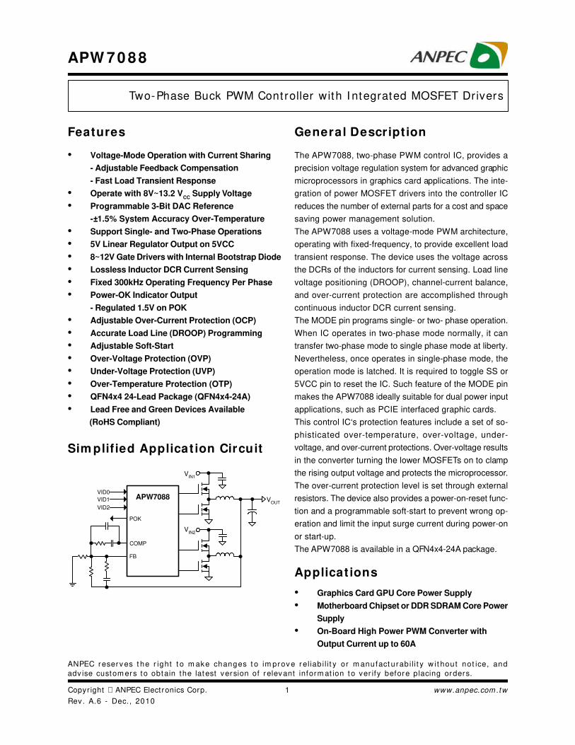
Copyright ANPEC Electronics Corp. Rev. A.6 - Dec., 2010 APW7088 www.anpec.com.tw 1 ANPEC reserves the right to make changes to improve reliability or manufacturability without notice, and advise customers to obtain the latest version of relevant information to verify before placing orders. Two-Phase Buck PWM Controller with Integrated MOSFET Drivers Features • Voltage-Mode Operation with Current Sharing - Adjustable Feedback Compensation - Fast Load Transient Response • Operate with 8V~13.2 V CC Supply Voltage • Programmable 3-Bit DAC Reference -±1.5% System Accuracy Over-Temperature • Support Single- and Two-Phase Operations • 5V Linear Regulator Output on 5VCC • 8~12V Gate Drivers with Internal Bootstrap Diode • Lossless Inductor DCR Current Sensing • Fixed 300kHz Operating Frequency Per Phase • Power-OK Indicator Output - Regulated 1.5V on POK • Adjustable Over-Current Protection (OCP) • Accurate Load Line (DROOP) Programming • Adjustable Soft-Start • Over-Voltage Protection (OVP) • Under-Voltage Protection (UVP) • Over-Temperature Protection (OTP) • QFN4x4 24-Lead Package (QFN4x4-24A) • Lead Free and Green Devices Available (RoHS Compliant) Applications General Description The APW7088, two-phase PWM control IC, provides a precision voltage regulation system for advanced graphic microprocessors in graphics card applications. The inte- gration of power MOSFET drivers into the controller IC reduces the number of external parts for a cost and space saving power management solution. The APW7088 uses a voltage-mode PWM architecture, operating with fixed-frequency, to provide excellent load transient response. The device uses the voltage across the DCRs of the inductors for current sensing. Load line voltage positioning (DROOP), channel-current balance, and over-current protection are accomplished through continuous inductor DCR current sensing. The MODE pin programs single- or two- phase operation. When IC operates in two-phase mode normally, it can transfer two-phase mode to single phase mode at liberty. Nevertheless, once operates in single-phase mode, the operation mode is latched. It is required to toggle SS or 5VCC pin to reset the IC. Such feature of the MODE pin makes the APW7088 ideally suitable for dual power input applications, such as PCIE interfaced graphic cards. This control IC‘s protection features include a set of so- phisticated over-temperature, over-voltage, under- voltage, and over-current protections. Over-voltage results in the converter turning the lower MOSFETs on to clamp the rising output voltage and protects the microprocessor. The over-current protection level is set through external resistors. The device also provides a power-on-reset func- tion and a programmable soft-start to prevent wrong op- eration and limit the input surge current during power-on or start-up. The APW7088 is available in a QFN4x4-24A package. • Graphics Card GPU Core Power Supply • Motherboard Chipset or DDR SDRAM Core Power Supply • On-Board High Power PWM Converter with Output Current up to 60A Simplified Application Circuit V IN1 V IN2 V OUT FB COMP APW7088 VID2 VID1 VID0 POK
Transcript of D:workingdatasheetAPWGreen - ChipBay · pok ss fb, × + × =
Copyr ight ANPEC Elect ronics Corp.
Rev. A.6 - Dec. , 2010
APW 7 0 8 8
www.anpec.com.tw1
ANPEC reserv es t he r ight t o m ake changes t o im prov e r el iab i li t y or m anufact urab i li t y w it hout not ice, and
adv ise custom ers to obtain the lat est version of relevant inform at ion t o ver ify before placing orders.
Two-Phase Buck PWM Controller with I ntegrated MOSFET Drivers
Features
• Voltage-Mode Operation with Current Sharing
- Adjustable Feedback Compensation
- Fast Load Transient Response
• Operate with 8V~13.2 VCC
Supply Voltage
• Programmable 3-Bit DAC Reference
-±1.5% System Accuracy Over-Temperature
• Support Single- and Two-Phase Operations
• 5V Linear Regulator Output on 5VCC
• 8~12V Gate Drivers with Internal Bootstrap Diode
• Lossless Inductor DCR Current Sensing
• Fixed 300kHz Operating Frequency Per Phase
• Power-OK Indicator Output
- Regulated 1.5V on POK
• Adjustable Over-Current Protection (OCP)
• Accurate Load Line (DROOP) Programming
• Adjustable Soft-Start
• Over-Voltage Protection (OVP)
• Under-Voltage Protection (UVP)
• Over-Temperature Protection (OTP)
• QFN4x4 24-Lead Package (QFN4x4-24A)
• Lead Free and Green Devices Available
(RoHS Compliant)
Applicat ions
General Description
The APW7088, two-phase PWM control IC, provides a
precision voltage regulation system for advanced graphic
microprocessors in graphics card applications. The inte-
gration of power MOSFET drivers into the controller IC
reduces the number of external parts for a cost and space
saving power management solution.
The APW7088 uses a voltage-mode PWM architecture,
operating with fixed-frequency, to provide excellent load
transient response. The device uses the voltage across
the DCRs of the inductors for current sensing. Load line
voltage positioning (DROOP), channel-current balance,
and over-current protection are accomplished through
continuous inductor DCR current sensing.
The MODE pin programs single- or two- phase operation.
When IC operates in two-phase mode normally, it can
transfer two-phase mode to single phase mode at liberty.
Nevertheless, once operates in single-phase mode, the
operation mode is latched. It is required to toggle SS or
5VCC pin to reset the IC. Such feature of the MODE pin
makes the APW7088 ideally suitable for dual power input
applications, such as PCIE interfaced graphic cards.
This control IC‘s protection features include a set of so-
phisticated over-temperature, over-voltage, under-
voltage, and over-current protections. Over-voltage results
in the converter turning the lower MOSFETs on to clamp
the rising output voltage and protects the microprocessor.
The over-current protection level is set through external
resistors. The device also provides a power-on-reset func-
tion and a programmable soft-start to prevent wrong op-
eration and limit the input surge current during power-on
or start-up.
The APW7088 is available in a QFN4x4-24A package.
• Graphics Card GPU Core Power Supply
• Motherboard Chipset or DDR SDRAM Core Power
Supply
• On-Board High Power PWM Converter with
Output Current up to 60A
Sim plified Applicat ion Circuit
VIN1
VIN2
VOUT
FB
COMP
APW7088
VID2
VID1
VID0
POK
Copyr ight ANPEC Elect ronics Corp.
Rev. A.6 - Dec. , 2010
APW 7 0 8 8
www.anpec.com.tw2
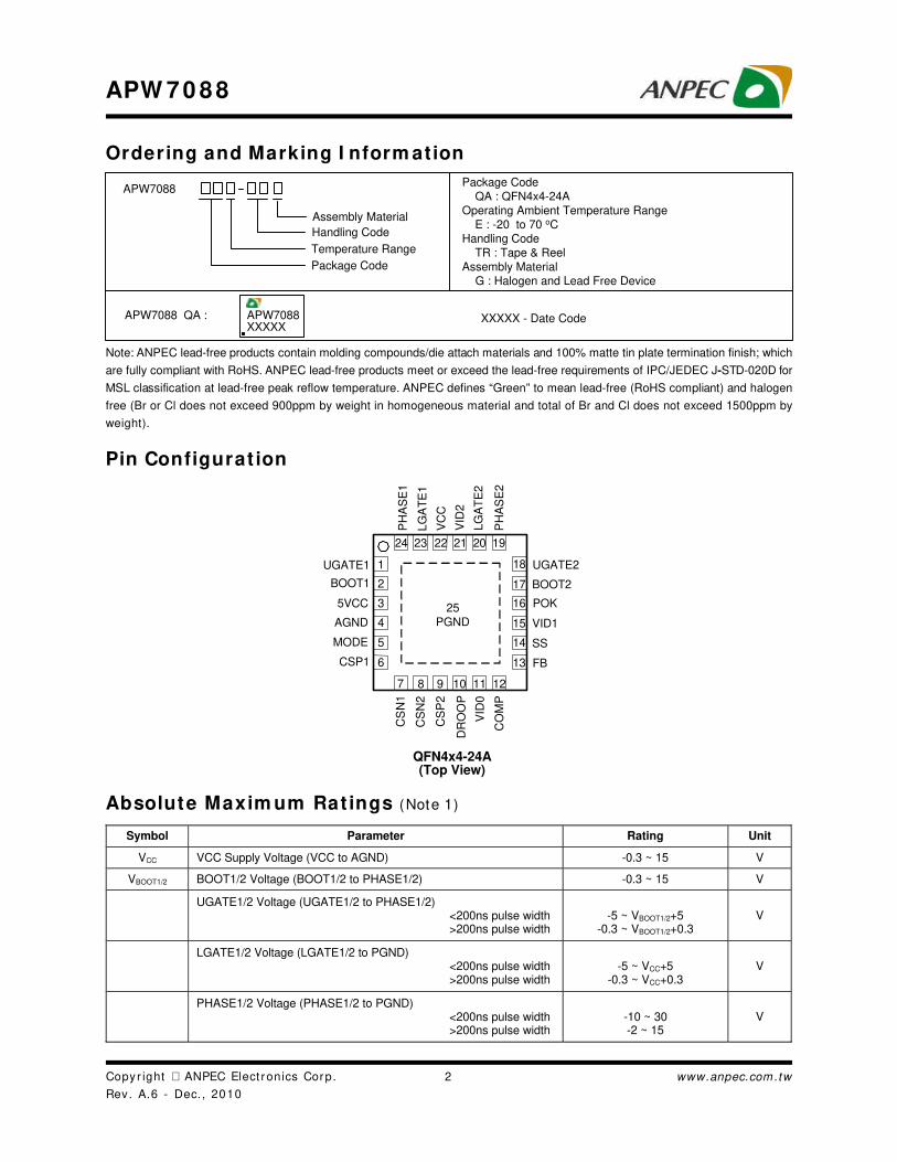
Ordering and Marking I nform ation
Absolute Maxim um Rat ings (Note 1)
Symbol Parameter Rating Unit
VCC VCC Supply Voltage (VCC to AGND) -0.3 ~ 15 V
VBOOT1/2 BOOT1/2 Voltage (BOOT1/2 to PHASE1/2) -0.3 ~ 15 V
UGATE1/2 Voltage (UGATE1/2 to PHASE1/2) <200ns pulse width >200ns pulse width
-5 ~ VBOOT1/2+5
-0.3 ~ VBOOT1/2+0.3 V
LGATE1/2 Voltage (LGATE1/2 to PGND) <200ns pulse width >200ns pulse width
-5 ~ VCC+5
-0.3 ~ VCC+0.3 V
PHASE1/2 Voltage (PHASE1/2 to PGND) <200ns pulse width >200ns pulse width
-10 ~ 30 -2 ~ 15
V
Pin Configurat ion
Note: ANPEC lead-free products contain molding compounds/die attach materials and 100% matte tin plate termination finish; which
are fully compliant with RoHS. ANPEC lead-free products meet or exceed the lead-free requirements of IPC/JEDEC J-STD-020D for
MSL classification at lead-free peak reflow temperature. ANPEC defines “Green” to mean lead-free (RoHS compliant) and halogen
free (Br or Cl does not exceed 900ppm by weight in homogeneous material and total of Br and Cl does not exceed 1500ppm by
weight).
QFN4x4-24A(Top View)
UGATE2
SS
CO
MP
VID
0
DR
OO
P
CS
P2
CS
N2
CS
N1
MODE
AGND
5VCC
BOOT1
UGATE1
CSP1
PH
AS
E2
LG
AT
E2
VID
2
VC
C
LG
AT
E1
PH
AS
E1
BOOT2
POK
VID1
FB
25
PGND
17
16
15
14
13
18
2
3
4
5
6
1
23 22 21 20 1924
8 9 10 11 127
APW7088
Handling Code
Temperature Range
Package Code
Package Code
QA : QFN4x4-24A
Operating Ambient Temperature Range
E : -20 to 70 oC
Handling Code
TR : Tape & Reel
Assembly Material
G : Halogen and Lead Free Device
Assembly Material
APW7088 QA : XXXXX - Date CodeAPW7088XXXXX
Copyr ight ANPEC Elect ronics Corp.
Rev. A.6 - Dec. , 2010
APW 7 0 8 8
www.anpec.com.tw3
Absolute Maxim um Rat ings ( Cont .) (Note 1)
Symbol Parameter Rating Unit
BOOT1/2 to AGND Voltage <200ns pulse width >200ns pulse width
-0.3 ~ 42 -0.3 ~ 30
V
V5VCC 5VCC Supply Voltage (5VCC to AGND, V5VCC < VCC +0.3V) -0.3 ~ 7 V
VMODE MODE to AGND Voltage -0.3 ~ 7 V
Input Voltage (SS, FB, COMP, DROOP, CSP1/2, CSN1/2, VID0/1/2 to
AGND) -0.3 ~ V5VCC +0.3 V
PGND to AGND Voltage -0.3 ~ +0.3 V
PDMAX Maximum Power Dissipation Limited Internally W
Maximum Junction Temperature 150 oC
TSTG Storage Temperature Range -65 ~ 150 oC
TSDR Maximum Soldering Temperature, 10 Seconds 260 oC
Note 1: Absolute Maximum Ratings are those values beyond which the life of a device may be impaired. Exposure to absolute maximum rating conditions for extended periods may affect device reliability.
Therm al Characterist ics
Recom m ended Operat ing Condit ions (Note 4)
Symbol Parameter Range Unit
VCC VCC Supply Voltage 8 ~ 13.2 V
V5VCC 5VCC Supply Voltage (V5VCC < VCC +0.3V) 5 ± 5% V
VOUT Converter Output Voltage 0.85 ~ 2.5 V
VIN1 PWM 1 Converter Input Voltage 3.1 ~ 13.2 V
VIN2 PWM 2 Converter Input Voltage 3.1 ~ 13.2 V
IOUT Converter Output Current ~ 60 A
TA Ambient Temperature -20 ~ 70 oC
TJ Junction Temperature -20 ~ 125 oC
CVCC Linear Regulator Output Capacitor 0.8 ~ 15 µF
C5VCC 5VCC Linear Regulator Output Capacitor 0.8 ~ 15 µF
Note 2 : θJA
is measured with the component mounted on a high effective thermal conductivity test board in free air. The exposed pad
of QFN4x4-24A is soldered directly on the PCB.
Note 3: The case temperature is measured at the center of the exposed pad on the underside of the QFN4x4-24A package.
Symbol Parameter Rating Unit
θJA Junction-to-Ambient Resistance
(Note 2)
QFN4x4-24A 45
θJC Junction-to-Case Resistance
(Note 3)
QFN4x4-24A 7
°C/W
Note 4 : Refer to the typical application circuits.

Copyr ight ANPEC Elect ronics Corp.
Rev. A.6 - Dec. , 2010
APW 7 0 8 8
www.anpec.com.tw4
Electrical Characterist ics
APW7088 Symbol Parameter Test Conditions
Min. Typ. Max. Unit
SUPPLY CURRENT
ICC VCC Nominal Supply Current UGATEx and LGATEx Open, FB forced above regulation point
- 5 10 mA
ISD VCC Shutdown Supply Current SS=GND - 5 - mA
POWER-ON-RESET (POR) AND OPERATION PHASE SELECTION
V5VCC_THR 5VCC Rising Threshold Voltage 4.2 4.5 4.8 V
5VCC POR Hysteresis 0.4 0.58 0.76 V
MODE Rising Threshold Voltage VMODE Rising 0.77 0.8 0.83 V
IMODE MODE Pin Input Current -100 - +100 nA
5VCC LINEAR REGULATOR
VREG_5VCC Output Voltage IO = 0A, VCC =8V 4.75 5 5.25 V
Line Regulation IO = 0A, VCC = 8V ~ 13.2V -20 - 20 mV
Load Regulation IO = 3mA, VCC > 8V -200 - 200 mV
Current-Limit 5VCC = GND 20 30 - mA
REFERENCE VOLTAGE
TA=25oC -1 - +1
Accuracy Over-temperature -1.5 - +1.5
%
IFB FB Pin Input Current -100 - +100 nA
VID0/1/2 Logic High Threshold 1.2 - - V
VID0/1/2 Logic Low Threshold - - 0.5 V
VID0/1/2 Pull-high Current - 1 - µA
VPOK POK Output Voltage - 1.5 - V
IO = 0~3mA, TA=25oC -2 - +2
POK Accuracy IO = 0~3mA, Over-temperature -3 - +3
%
POK Current-Limit POK = GND 4 8 15 mA
POK Pull-Low Resistance IPOK = 5mA - 70 100 Ω
ERROR AMPLIFIER
DC Gain RL = 10kΩ to the ground - 85 - dB
Gain-Bandwidth Product CL = 100pF, RL = 10kΩ to the ground - 20 - MHz
Slew Rate CL = 100pF, IO = ±400µA - 8 - V/µs
Upper Clamp Voltage IO = 1mA 2.7 3.0 - V
Lower Clamp Voltage IO = -1mA - - 0.1 V
COMP Pull-Low Resistance In fault or shutdown condition - 2 - kΩ
OSCILLATOR
FOSC Oscillator Frequency 255 300 345 kHz
∆VOSC1/2 Oscillator Sawtooth Amplitude - 1.5 - V
Maximum Duty Cycle 85 88 - %
Refer to the typical application circuits. These specifications apply over VIN
=12V, VOUT
=1.2V and TA= -20 ~ 70°C, unless otherwise
specified. Typical values are at TA=25°C. The V
5VCC is supplied by the internal regulator.

Copyr ight ANPEC Elect ronics Corp.
Rev. A.6 - Dec. , 2010
APW 7 0 8 8
www.anpec.com.tw5
Electrical Characterist ics ( Cont .)Refer to the typical application circuits. These specifications apply over VIN=12V, VOUT=1.2V and TA= -20 ~ 70°C, unless otherwise
specified. Typical values are at TA=25°C. The V5VCC is supplied by the internal regulator.
APW7088 Symbol Parameter Test Conditions
Min. Typ. Max. Unit
MOSFET GATE DRIVERS
UGATE1/2 Source Current VBOOT = 12V, VUGATE-VPHASE = 2V - 2.6 - A
UGATE1/2 Sink Current VBOOT = 12V, VUGATE-VPHASE = 2V - 1 - A
LGATE1/2 Source Current VCC = 12V, VLGATE = 2V - 2.6 - A
LGATE1/2 Sink Current VCC =12V, VLGATE = 2V - 1.4 - A
UGATE1/2 Source Resistance VBOOT = 12V, 100mA Source Current - 2.5 3.75 Ω
UGATE1/2 Sink Resistance VBOOT = 12V, 100mA Sink Current - 2 3 Ω
LGATE1/2 Source Resistance VCC = 12V, 100mA Source Current - 2 3 Ω
LGATE1/2 Sink Resistance VCC = 12V, 100mA Sink Current - 1.4 2.1 Ω
TD Dead-Time - 30 - ns
CURRENT SENSE AND DROOP FUNCTION
ICSP CSP1/2 Pin Input Current -100 - +100 nA
Sourcing current 80 - - ICSN CSN1/2 Maximum Output Current R CSN1/2 = 2kΩ,
Sinking current 15 - - µA
Current Sense Amplifier Bandwidth - 3 - MHz
DROOP Output Current Accuracy RDROOP = 2kΩ, VDROOP =0.005V - 50 - µA
DROOP Accuracy ∆VFB = VDROOP/20, VDROOP=1V -5 - +5 mV
Current Difference Between
Channel1/2 and Average Current -10 - +10 %
SOFT-START AND ENABLE
ISS Soft-Start Current Source Flowing out of SS pin 8 10 12 µA
Soft-Start Complete Threshold - 3.2 - V
SS Pull-low Resistance - 10 18 kΩ
POWER OK AND PROTECTIONS
Over-Current Trip Level ICS1 + ICS2 110 120 140 µA
VUV FB Under-Voltage Threshold ~ 2µs noise filter, VFB falling,
Percentage of VR at Error Amplifier 40 50 60 %
VPOK_L POK Lower Threshold - 87.5 - %
VOV,
VPOK_H
FB Over-Voltage Threshold
and POK Upper Threshold
~ 2µs noise filter, VFB rising
Percentage of VR at Error Amplifier 115 125 135 %
FB Over-Voltage Hysteresis - 60 80 mV
TOTR Over-Temperature Trip Level TJ rising - 150 - oC
Over-Temperature Hysteresis - 50 - oC
Copyr ight ANPEC Elect ronics Corp.
Rev. A.6 - Dec. , 2010
APW 7 0 8 8
www.anpec.com.tw6
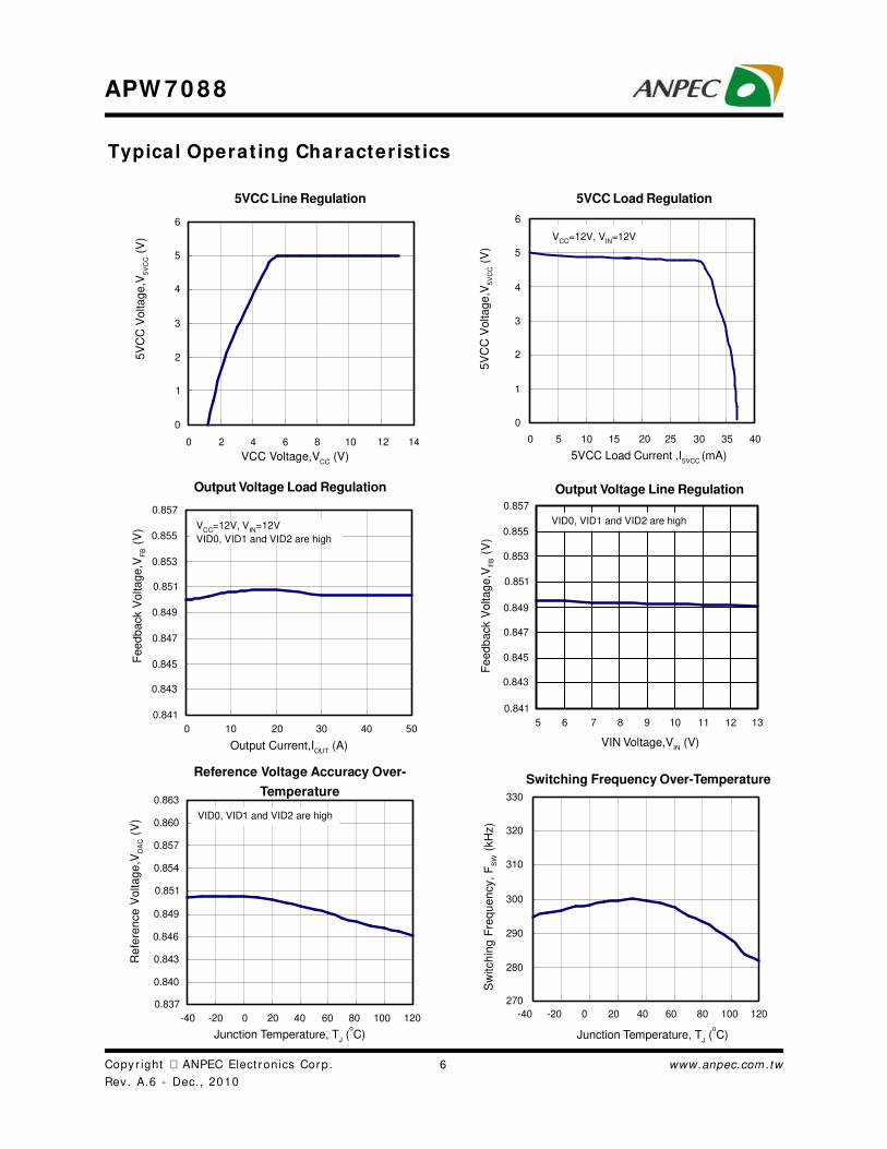
Typical Operat ing Characterist ics
Reference Voltage Accuracy Over-
Temperature
Junction Temperature, TJ (
oC)
Re
fere
nce
Vo
lta
ge
,VD
AC (
V)
Output Voltage Load Regulation
Output Current,IOUT
(A)
Output Voltage Line Regulation
VIN Voltage,VIN
(V)
5VCC Line Regulation 5VCC Load Regulation
VCC Voltage,VCC
(V) 5VCC Load Current ,I5VCC
(mA)
5V
CC
Voltage,V
5V
CC (
V)
5V
CC
Voltage,V
5V
CC (
V)
Fe
ed
ba
ck V
olta
ge
,VF
B (
V)
Fe
ed
ba
ck V
olta
ge
,VF
B (
V)
Sw
itch
ing
Fre
qu
en
cy,
FS
W (
kH
z)
Switching Frequency Over-Temperature
0
1
2
3
4
5
6
0 2 4 6 8 10 12 14
270
280
290
300
310
320
330
-40 -20 0 20 40 60 80 100 120
0
1
2
3
4
5
6
0 5 10 15 20 25 30 35 40
VCC
=12V, VIN
=12V
Junction Temperature, TJ (
oC)
0 10 20 30 40 50
0.841
0.843
0.845
0.847
0.849
0.851
0.853
0.855
0.857
VCC
=12V, VIN
=12V
VID0, VID1 and VID2 are high
0.841
0.843
0.845
0.847
0.849
0.851
0.853
0.855
0.857
5 6 7 8 9 10 11 12 13
VID0, VID1 and VID2 are high
0.837
0.840
0.843
0.846
0.849
0.851
0.854
0.857
0.860
0.863
-40 -20 0 20 40 60 80 100 120
VID0, VID1 and VID2 are high
Copyr ight ANPEC Elect ronics Corp.
Rev. A.6 - Dec. , 2010
APW 7 0 8 8
www.anpec.com.tw7
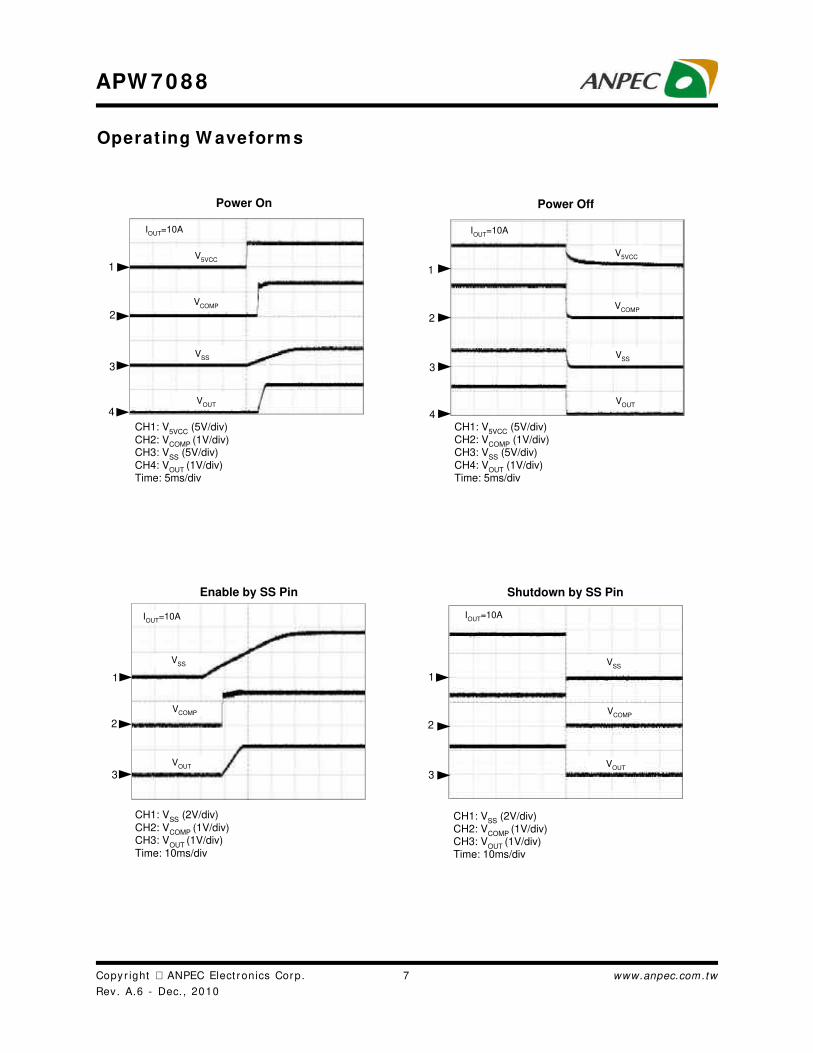
Operat ing W aveform s
CH1: V5VCC
(5V/div)
CH2: VCOMP (1V/div)CH3: V
SS (5V/div)
CH4: VOUT
(1V/div)
Time: 5ms/div
Power On
IOUT
=10A
1
2
3
4
V5VCC
VCOMP
VSS
VOUT
CH1: V5VCC
(5V/div)CH2: V
COMP (1V/div)
CH3: VSS
(5V/div)CH4: V
OUT (1V/div)
Time: 5ms/div
Power Off
IOUT
=10A
1
2
3
4
V5VCC
VCOMP
VSS
VOUT
CH1: VSS
(2V/div)
CH2: VCOMP
(1V/div)CH3: V
OUT (1V/div)
Time: 10ms/div
Enable by SS Pin
IOUT
=10A
1
2
3
VCOMP
VSS
VOUT
Shutdown by SS Pin
CH1: VSS
(2V/div)
CH2: VCOMP
(1V/div)CH3: V
OUT (1V/div)
Time: 10ms/div
IOUT
=10A
1
2
3
VCOMP
VSS
VOUT

Copyr ight ANPEC Elect ronics Corp.
Rev. A.6 - Dec. , 2010
APW 7 0 8 8
www.anpec.com.tw8
Operat ing W aveform s ( Cont.)
Power On Without VIN2
Voltage
CH1: VOUT
(1V/div)
CH2: VPHASE1
(10V/div)
CH3: VPHASE2
(2V/div)
CH4: VSS
(2V/div)
Time: 5ms/div
1
2
3
4
VOUT
VPHASE1
VPHASE2
Vss
Under-Voltage Protection (UVP)
CH1: VFB
(500mV/div)
CH2: VPHASE1
(10V/div)
CH3: VPHASE2
(10V/div)
CH4: VSS
(2V/div)
Time: 500µs/div
1
2
3
4
VFB
VPHASE1
VPHASE2
Vss
CH1: VPHASE1
(20V/div)
CH2: IPHASE2
(20A/div)
CH3: VOUT
(AC, 200mV/div)CH4: I
OUT (10A/div)
Time: 20µs/div
Load Transient , 40A==>0A
RSEN
=3kΩL=0.56µH
DCR=4mΩ
1
2
3
4
VOUT
VPHASE1
IPHASE2
IOUT
Load Transient , 0A==>40A
CH1: VPHASE1
(20V/div)
CH2: IPHASE2
(20A/div)
CH3: VOUT
(AC, 200mV/div)
CH4: IOUT
(10A/div)
Time: 20µs/div
1
2
3
4
VPHASE1
IPHASE2
VOUT
RSEN
=3kΩL=0.56µH
DCR=4mΩIOUT
Copyr ight ANPEC Elect ronics Corp.
Rev. A.6 - Dec. , 2010
APW 7 0 8 8
www.anpec.com.tw9
Operat ing W aveform s ( Cont.)
CH1: IL1
(10A/div)
CH2: IL2
(10A/div)
CH3: VSS
(5V/div)CH4: V
OUT (1V/div)
Time: 5ms/div
OCP at Slow Slew IOUT
RSEN
=1.5kΩL=0.56µH
DCR=4mΩ1
2
3
4
VSS
IL1
IL2
VOUT
Short-Circuit Test After Power On
RSEN
=1.5kΩL=0.56µH
DCR=4mΩ
CH1: IL1
(10A/div)
CH2: IL2
(10A/div)
CH3: VSS
(5V/div)
CH4: VOUT
(1V/div)
Time: 5ms/div
1
2
3
4
VSS
IL1
IL2
VOUT
Short-Circuit Test Before Power On
RSEN
=1.5kΩL=0.56µH
DCR=4mΩ
CH1: IL1
(10A/div)
CH2: IL2
(10A/div)
CH3: VSS
(5V/div)CH4: V
OUT (1V/div)
Time: 5ms/div
1
2
3
4
IL1
IL2
VSS
VOUT
OVP After Power On
Pull-Up VFB
> V OV
CH1: VFB
(500mV/div)
CH2: VSS
(2V/div)
CH3: VLG1
(10V/div)
CH4: VLG2
(10V/div)
Time: 100µs/div
1
2
3
4
VFB
VSS
VLG1
VLG2
Copyr ight ANPEC Elect ronics Corp.
Rev. A.6 - Dec. , 2010
APW 7 0 8 8
www.anpec.com.tw10
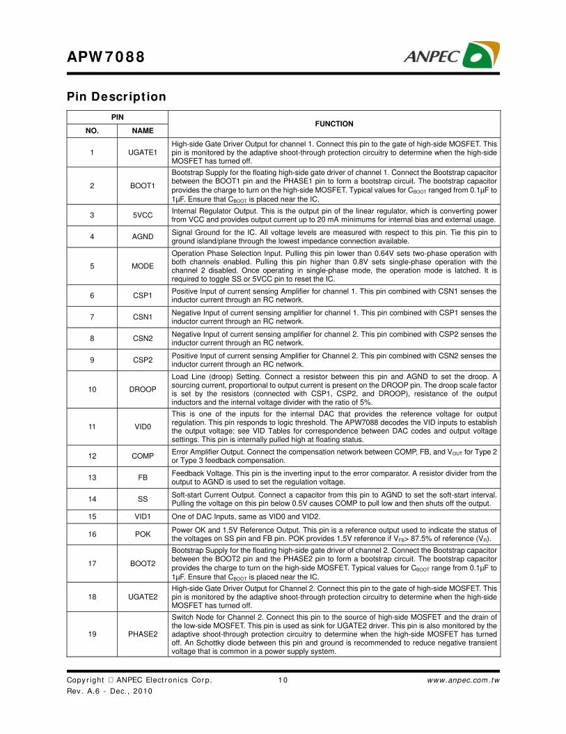
Pin Descript ion
PIN
NO. NAME FUNCTION
1 UGATE1 High-side Gate Driver Output for channel 1. Connect this pin to the gate of high-side MOSFET. This pin is monitored by the adaptive shoot-through protection circuitry to determine when the high-side MOSFET has turned off.
2 BOOT1
Bootstrap Supply for the floating high-side gate driver of channel 1. Connect the Bootstrap capacitor between the BOOT1 pin and the PHASE1 pin to form a bootstrap circuit. The bootstrap capacitor
provides the charge to turn on the high-side MOSFET. Typical values for CBOOT ranged from 0.1µF to
1µF. Ensure that CBOOT is placed near the IC.
3 5VCC Internal Regulator Output. This is the output pin of the linear regulator, which is converting power from VCC and provides output current up to 20 mA minimums for internal bias and external usage.
4 AGND Signal Ground for the IC. All voltage levels are measured with respect to this pin. Tie this pin to ground island/plane through the lowest impedance connection available.
5 MODE
Operation Phase Selection Input. Pulling this pin lower than 0.64V sets two-phase operation with both channels enabled. Pulling this pin higher than 0.8V sets single-phase operation with the channel 2 disabled. Once operating in single-phase mode, the operation mode is latched. It is required to toggle SS or 5VCC pin to reset the IC.
6 CSP1 Positive Input of current sensing Amplifier for channel 1. This pin combined with CSN1 senses the inductor current through an RC network.
7 CSN1 Negative Input of current sensing amplifier for channel 1. This pin combined with CSP1 senses the inductor current through an RC network.
8 CSN2 Negative Input of current sensing amplifier for channel 2. This pin combined with CSP2 senses the inductor current through an RC network.
9 CSP2 Positive Input of current sensing Amplifier for Channel 2. This pin combined with CSN2 senses the inductor current through an RC network.
10 DROOP
Load Line (droop) Setting. Connect a resistor between this pin and AGND to set the droop. A sourcing current, proportional to output current is present on the DROOP pin. The droop scale factor is set by the resistors (connected with CSP1, CSP2, and DROOP), resistance of the output inductors and the internal voltage divider with the ratio of 5%.
11 VID0
This is one of the inputs for the internal DAC that provides the reference voltage for output regulation. This pin responds to logic threshold. The APW7088 decodes the VID inputs to establish the output voltage; see VID Tables for correspondence between DAC codes and output voltage settings. This pin is internally pulled high at floating status.
12 COMP Error Amplifier Output. Connect the compensation network between COMP, FB, and VOUT for Type 2 or Type 3 feedback compensation.
13 FB Feedback Voltage. This pin is the inverting input to the error comparator. A resistor divider from the output to AGND is used to set the regulation voltage.
14 SS Soft-start Current Output. Connect a capacitor from this pin to AGND to set the soft-start interval. Pulling the voltage on this pin below 0.5V causes COMP to pull low and then shuts off the output.
15 VID1 One of DAC Inputs, same as VID0 and VID2.
16 POK Power OK and 1.5V Reference Output. This pin is a reference output used to indicate the status of the voltages on SS pin and FB pin. POK provides 1.5V reference if VFB> 87.5% of reference (VR).
17 BOOT2
Bootstrap Supply for the floating high-side gate driver of channel 2. Connect the Bootstrap capacitor between the BOOT2 pin and the PHASE2 pin to form a bootstrap circuit. The bootstrap capacitor
provides the charge to turn on the high-side MOSFET. Typical values for CBOOT range from 0.1µF to
1µF. Ensure that CBOOT is placed near the IC.
18 UGATE2 High-side Gate Driver Output for Channel 2. Connect this pin to the gate of high-side MOSFET. This pin is monitored by the adaptive shoot-through protection circuitry to determine when the high-side MOSFET has turned off.
19 PHASE2
Switch Node for Channel 2. Connect this pin to the source of high-side MOSFET and the drain of the low-side MOSFET. This pin is used as sink for UGATE2 driver. This pin is also monitored by the adaptive shoot-through protection circuitry to determine when the high-side MOSFET has turned off. An Schottky diode between this pin and ground is recommended to reduce negative transient voltage that is common in a power supply system.

Copyr ight ANPEC Elect ronics Corp.
Rev. A.6 - Dec. , 2010
APW 7 0 8 8
www.anpec.com.tw11
Pin Descript ion ( Cont .)
PIN
NO. NAME FUNCTION
20 LGATE2 Low-side Gate Driver Output for Channel 2. Connect this pin to the gate of low-side MOSFET. This pin is monitored by the adaptive shoot-through protection circuitry to determine when the low-side MOSFET has turned off.
21 VID2 One of DAC Inputs, same as VID0 and VID1.
22 VCC Supply Voltage Input. This pin provides bias supply for the low-side gate drivers and the bootstrap circuit for high-side drivers. This pin can receive a well-decoupled 8V~13.2V supply voltage. Ensure that this pin is bypassed by a ceramic capacitor next to the pin.
23 LGATE1 Low-side Gate Driver Output for Channel 1. Connect this pin to the gate of low-side MOSFET. This pin is monitored by the adaptive shoot-through protection circuitry to determine when the low-side MOSFET has turned off.
24 PHASE1
Switch Node for Channel 1. Connect this pin to the source of high-side MOSFET and the drain of the low-side MOSFET. This pin is used as sink for UGATT1 driver. This pin is also monitored by the adaptive shoot-through protection circuitry to determine when the high-side MOSFET has turned off. An Schottky diode between this pin and ground is recommended to reduce negative transient voltage, which is common in a power supply system.
25 PGND Power Ground for the low-side gate drivers. Connect this pin to the source of low-side MOSFETs. This pin is used as sink for LGATE1 and LGATE2 drivers.

Copyr ight ANPEC Elect ronics Corp.
Rev. A.6 - Dec. , 2010
APW 7 0 8 8
www.anpec.com.tw12
Block Diagram
PGND
MODE
DROOP
ErrorAmplifier
FB
UGATE2
LGATE2
BOOT2
PHASE2
UGATE1
LGATE1
BOOT1
PHASE1
Current
BalanceICS2
CSP2CSN2
CSP1CSN1I
CS1
120µAOC
Droop Control
VCC
Power-on-Reset
5VCC5VCC
Linear
RegulatorVCC
Oscillator
and
Sawtooth
Control
Logic
Soft-Start SS
V5VCC
3.6V
ISS
10µA
VCC
VCC
300kHz
Current
Sense
Current
Sense
-
+
COMPV
OSC1
VOSC2
VCC V
CC
SS
EN
D
1.5V
Reference
OV
UV
POK
125%
50%
VR
Over-Temperature
Protection
ICS1
+ICS2
ICS1
+ICS2
Operation
Phase
Selection
87.5%
AGND
VID03-BitDAC
VID1
VID2V
DAC
VDROOP
PWM Signal Controller
Copyr ight ANPEC Elect ronics Corp.
Rev. A.6 - Dec. , 2010
APW 7 0 8 8
www.anpec.com.tw13
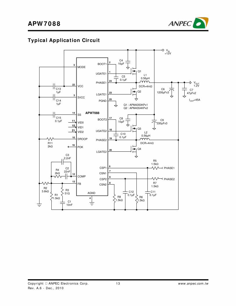
Typical Applicat ion Circuit
Q1 : APM4350KPx1
Q2 : APM4354KPx2
VIN
+12V
BOOT1
UGATE1
PHASE1
LGATE1
C5
0.1µF
C6
1200µFx3
L1
0.56µH
C4
10µF
Q2
Q1
VOUT
1.2V
C7
47µFx2
BOOT2
UGATE2
PHASE2
LGATE2
C10
0.1µF
L20.56µH
C8
10µF
Q4
Q3
C9
330µFx3
MODE
VCC
5VCC
SS
DROOP
R11
2kΩ
C15
0.1µF
C13
1µF
C14
1µF
APW7088
PGND
1
25
23
24
25
17
18
19
20
22
3
14
10
DCR=4mΩ
DCR=4mΩ
IOCP
=45A
CSP1
CSN1
CSP2
CSN2
R8
1.5kΩ
R5
1.5kΩ
R7
1.5kΩ
C12
0.1µF
C11
0.1µF
PHASE1
PHASE2
FB
POK
R6
1.5kΩ
AGND
7
6
9
8
16
4
COMP
R1
1.5kΩ
R23.6kΩ
13
12
R3
51Ω
C1
10nF
C3
2.2nF
C2
22nFR4
2kΩ
VID2
VID1
VID0
21
15
11
Copyr ight ANPEC Elect ronics Corp.
Rev. A.6 - Dec. , 2010
APW 7 0 8 8
www.anpec.com.tw14
Funct ion Descript ion
5VCC Linear Regulator
5VCC is the output terminal of the internal 5V linear
regulator which regulates a 5V voltage on 5VCC by
controlling an internal bypass transistor between VCC
and 5VCC. The linear regulator powers the internal
control circuitry and is stable with a low-ESR ceramic
output capacitor. Bypass 5VCC to GND with a ceramic
capacitor of at least 1µF. Place the capacitor physically
close to the IC to provide good noise decoupling. The
linear regulator can also provide output current, up to
20mA, for external loads. The linear regulator with current-
limit protection can protect itself during over-load or short-
circuit conditions on 5VCC pin.
The 5VCC linear regulator stop regulating in Over-Tem-
perature Protection. When the junction temperature is
cooled by 50oC, the 5VCC linear regulator starts to regu-
late the output voltage again.
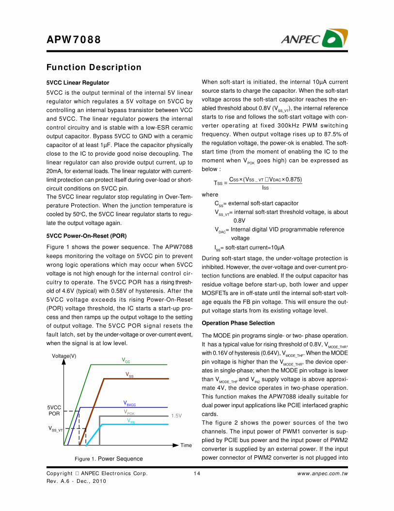
5VCC Power-On-Reset (POR)
Figure 1 shows the power sequence. The APW7088
keeps monitoring the voltage on 5VCC pin to prevent
wrong logic operations which may occur when 5VCC
voltage is not high enough for the internal control cir-
cuitry to operate. The 5VCC POR has a rising thresh-
old of 4.6V (typical) with 0.58V of hysteresis. After the
5VCC voltage exceeds i ts rising Power-On-Reset
(POR) voltage threshold, the IC starts a start-up pro-
cess and then ramps up the output voltage to the setting
of output voltage. The 5VCC POR signal resets the
fault latch, set by the under-voltage or over-current event,
when the signal is at low level.
Figure 1. Power Sequence
When soft-start is initiated, the internal 10µA current
source starts to charge the capacitor. When the soft-start
voltage across the soft-start capacitor reaches the en-
abled threshold about 0.8V (VSS_VT
), the internal reference
starts to rise and follows the soft-start voltage with con-
verter operating at fixed 300kHz PWM switching
frequency. When output voltage rises up to 87.5% of
the regulation voltage, the power-ok is enabled. The soft-
start time (from the moment of enabling the IC to the
moment when VPOK
goes high) can be expressed as
below :
where
CSS
= external soft-start capacitor
VSS_VT
= internal soft-start threshold voltage, is about
0.8V
VDAC
= Internal digital VID programmable reference
voltage
ISS
= soft-start current=10µA
During soft-start stage, the under-voltage protection is
inhibited. However, the over-voltage and over-current pro-
tection functions are enabled. If the output capacitor has
residue voltage before start-up, both lower and upper
MOSFETs are in off-state until the internal soft-start volt-
age equals the FB pin voltage. This will ensure the out-
put voltage starts from its existing voltage level.
VCC
V5VCC
5VCC
POR
VSS
VFB
VPOK
1.5V
VSS_VT
Voltage(V)
Time
Operation Phase Selection
The MODE pin programs single- or two- phase operation.
It has a typical value for rising threshold of 0.8V, VMODE_THR
,
with 0.16V of hysteresis (0.64V), VMODE_THF
. When the MODE
pin voltage is higher than the VMODE_THR
, the device oper-
ates in single-phase; when the MODE pin voltage is lower
than VMODE_THF
and VIN2
supply voltage is above approxi-
mate 4V, the device operates in two-phase operation.
This function makes the APW7088 ideally suitable for
dual power input applications like PCIE interfaced graphic
cards.
The figure 2 shows the power sources of the two
channels. The input power of PWM1 converter is sup-
plied by PCIE bus power and the input power of PWM2
converter is supplied by an external power. If the input
power connector of PWM2 converter is not plugged into
SS
DACVT_SSSSSS
I
)875.0VV(CT
×+×=

Copyr ight ANPEC Elect ronics Corp.
Rev. A.6 - Dec. , 2010
APW 7 0 8 8
www.anpec.com.tw15
Funct ion Descript ion ( Cont .)
Operation Phase Selection (Cont.)
Figure 2. VIN2
Sensing Circuit
Over-Voltage Protection (OVP)
The over-voltage protection function monitors the output
voltage through FB pin. When the FB voltage increases
over 125% of the reference voltage (VR) due to the high-
side MOSFET failure or other reasons, the over-voltage
protection comparator designed with a 2µs noise filter
will force the low-side MOSFET gate drivers high. This
action actively pulls down the output voltage and eventu-
ally attempts to trigger the over-current shutdown of an
ATX power supply. As soon as the output voltage is within
regulation, the OVP comparator is disengaged. The chip
will restore its normal operation. When the OVP occurs,
the POK will drop to low as well.
This OVP scheme only clamps the voltage overshoot
and does not invert the output voltage when otherwise
activated with a continuously high output from low-side
MOSFETs driver, which is a common problem for OVP
schemes with a latch.
Under-Voltage Protection (UVP)
In the operational process, when a short-circuit occurs,
the output voltage will drop quickly. Before the over-cur-
PWM 1converter
PCIE +12V
PWM 2
converter
ExternalPower V
IN2
PHASE2
VCC
4V
MODE
VIN2
sensing
circuit
Operation
Phase
Selection
Figure 3 shows the circuit of sensing inductor current.
Connecting a series resistor (RS) and a capacitor (C
S)
network in parallel with the inductor and measuring
the voltage (VC) across the capacitor can sense the in-
ductor current.
Figure 3. Illustration of Inductor Current Sensing Circuit
Over-Current Protection (OCP)
L DCR
Rs C
s
R2
CSP
CSN
PHASE
IL
VC
VL
the socket before start-up, the internal VIN2
sensing circuit
can sense the absence of VIN2
and set the IC to operate in
single-phase mode with PWM2 disabled. When the IC
operates in two-phase mode, it can switch the operating
mode from two-phase to single-phase operation. Once
operating in single-phase mode, the operation mode is
latched. It is required to toggle SS or 5VCC pin to reset
the IC.
rent protection responds, the output voltage will fall
out of the required regulation range. The under-voltage
continually monitors the VFB
voltage after soft-start is
completed. If a load step is strong enough to pull the
output voltage lower than the under-voltage threshold,
the IC shuts down converter’s output. Cycling the 5VCC
POR resets the fault latch and starts a start-up process.
The under-voltage threshold is 50% of the nominal out-
put voltage. The under-voltage comparator has a built-in
2µs noise filter to prevent the chips from wrong UVP
shutdown being caused by noise.
The equations of the sensing network are,
Take
for example, if the above is true, the voltage across the
capacitor CS is equal to voltage drop across the inductor
DCR, and the voltage VC is proportional to the current I
L.
The sensing current through the resistor R2 can be ex-
pressed as below :
L LV (s)=I (s) (SL+DCR)×
SS
L
SSLC
CSR1
)DCRSL()S(I
CSR1
1(S)V(S)V
++×=
+×=
DCR
LCR SS =
R2
DCRII
LCS
×=

Copyr ight ANPEC Elect ronics Corp.
Rev. A.6 - Dec. , 2010
APW 7 0 8 8
www.anpec.com.tw16
Funct ion Descript ion ( Cont .)
where
ICS
is the sensed current
IL is the inductor current
DCR is the inductor resistance
R2 is the sense resistor
Over-Current Protection (OCP) (Cont.)
The APW7088 is a two-phase PWM controller; therefore,
the IC has two sensed current parts, ICS1
and ICS2
. When
ICS1
plus ICS2
is greater than 120µA, the over-current occurs.
In over-current protection, the IC shuts off the converter
and then initials a new soft-start process. After 3 over-
current events are counted, the device turns off both high-
side and low-side MOSFETs and the converter’s output
is latched to be floating.
DROOP
In some high current applications, a requirement on
precisely controlled output impedance is imposed. This
dependence of output voltage on load current is often
termed droop regulation.
As shown in figure 4, the droop control block gener-
ates a voltage through external resistor RDROOP
, then
set the droop voltage. The droop voltage, VDROOP
, is
proportional to the total current in two channels. As
the following equation shows,
The VDROOP
voltage is used the regulator to adjust the out-
put voltage so that it’s equal to the reference voltage mi-
nus the droop voltage.
Over-Temperature Protection (OTP)
When the junction temperature increases above the ris-
ing threshold temperature TOTR
, the IC will enter the over-
temperature protection state that suspends the PWM,
which forces the LGATE and UGATE gate drivers to out-
put low voltages and turns off the 5VCC linear regulator
output. The thermal sensor allows the converters to start
a start-up process and regulate the output voltage again
after the junction temperature cools by 50oC. The OTP is
designed with a 50oC hysteresis to lower the average TJ
during continuous thermal overload conditions, which
increases lifetime of the APW7088.
Current Sharing
The APW7088 uses inductor’s DCRs and external net-
works to sense the both currents flowing through the in-
ductors of the PWM1 and PWM2 channels. The current
sharing circuit, with closed-loop control, uses the sensed
currents to adjust the two-phase inductor currents. For
example, if the sensed current of PWM1 is bigger than
PWM2, the duty of PWM1 will decrease and the duty of
PWM2 will increase. Then, the device will reduce IL1
current and increase IL2
current for current sharing.VID2 VID1 VID0
DAC Output Voltage, VDAC (V)
0 0 0 1.20
0 0 1 1.15
0 1 0 1.10
0 1 1 1.05
1 0 0 1.00
1 0 1 0.95
1 1 0 0.90
1 1 1 0.85
Table 1. DAC Output Voltage vs. VID Inputs
Figure 4. Illustration of Droop Setting Function
Droop Control
VR
VREFIN/EN
or 0.6V
RDROOP
VDROOP
]R)II[(05.0V DROOP2CS1CSDROOP ×+×=

Copyr ight ANPEC Elect ronics Corp.
Rev. A.6 - Dec. , 2010
APW 7 0 8 8
www.anpec.com.tw17
Applicat ion I nform at ion
Output Voltage Setting
Where VDAC
is the internal digital VID programmable ref-
erence voltage, the RTOP
is the resistor connected from
converter’s output to FB and RGND
is the resistor con-
nected from FB to AGND. Suggested RGND
is in the range
from 1K to 20KΩ. To prevent stray pickup, locate resis-
tors RTOP
and RGND
close to the APW7088.
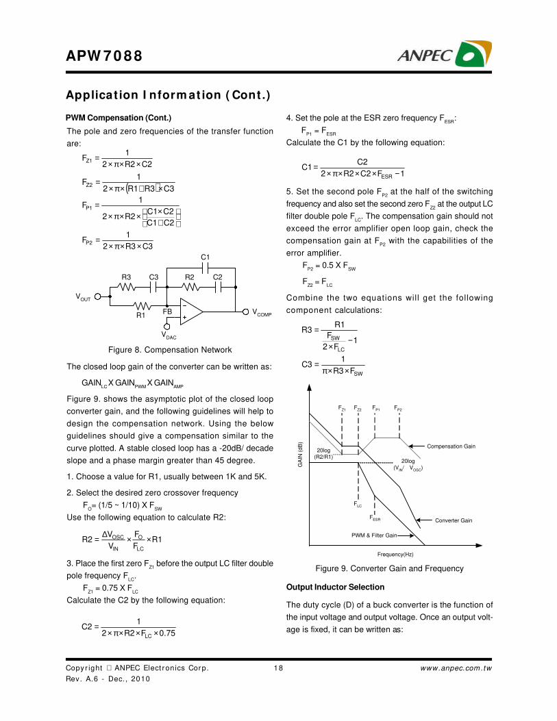
PWM Compensation
The output LC filter of a step down converter introduces a
double pole, which contributes with -40dB/decade gain
slope and 180 degrees phase shift in the control loop. A
compensation network among COMP, FB, and VOUT
should be added. The compensation network is shown
in Figure 8. The output LC fi l ters consists of the
output inductors and output capacitors. For two-phase
convertor, when assuming VIN1
=VIN2
=VIN
, L1=L2=L, the
transfer function of the LC filter is given by :
The poles and zero of this transfer functions are :
The FLC
is the double-pole frequency of the two-phase LC
filters, and FESR
is the frequency of the zero introduced by
the ESR of the output capacitors.
1CESRsCL2
1s
CESRs1GAIN
OUTUTO2
OUTLC
+××+××
××+=
OUT
LC
CL2
12
1F
××π×=
OUTESR
CESR2
1F
××π×=
Figure 5. The Output LC Filter
Figure 6. Frequency Resopnse of the LC Filters
FLC
FESR
-40dB/dec
-20dB/dec
Frequency(Hz)
GA
IN (
dB
)
The PWM modulator is shown in figure 7. The input is the
output of the error amplifier and the output is the PHASE
node. The transfer function of the PWM modulator is given
by :
Figure 7. The PWM Modulator
The compensation network is shown in figure 8. It pro-
vides a close loop transfer function with the highest zero
crossover frequency and sufficient phase margin.
The transfer function of error amplifier is given by:
( )
×+×
××++
×+
+×
×+
×××
+=
C3R3
1s
C2C1R2
C2C1ss
C3R3R1
1s
C2R2
1s
C1R3R1
R3R1
+
+
==
sC3
1R3R1//
sC2
1R2//
sC1
1
V
VGAIN
OUT
COMPAMP
OSC
INPWM
V
VGAIN
∆=
OSC
Output of ErrorAmplifier
∆VOSC
PWMComparator
Driver
Driver
PHASE
VIN
The output voltage is adjustable from 0.85V to 2.5V with a
resistor-divider connected with FB, AGND, and converter’s
output. Using 1% or better resistors for the resistor-di-
vider is recommended. The output voltage is determined
by :
+×=
GND
TOPDACOUT
R
R1VV
VPHASE1
L1=L VOUT
COUT
ESR
VPHASE2
L2=L
Copyr ight ANPEC Elect ronics Corp.
Rev. A.6 - Dec. , 2010
APW 7 0 8 8
www.anpec.com.tw18
Applicat ion I nform at ion ( Cont .)
PWM Compensation (Cont.)
The pole and zero frequencies of the transfer function
are:
Figure 8. Compensation Network
C2R22
1FZ1 ××π×
=
( ) C3R3R12
1FZ2 ×+×π×
=
+×××π×
=
C2C1
C2C1R22
1FP1
C3R32
1FP2 ××π×
=
The closed loop gain of the converter can be written as:
GAINLC
X GAINPWM
X GAINAMP
Figure 9. shows the asymptotic plot of the closed loop
converter gain, and the following guidelines will help to
design the compensation network. Using the below
guidelines should give a compensation similar to the
curve plotted. A stable closed loop has a -20dB/ decade
slope and a phase margin greater than 45 degree.
1. Choose a value for R1, usually between 1K and 5K.
2. Select the desired zero crossover frequency
FO= (1/5 ~ 1/10) X F
SW
Use the following equation to calculate R2:
3. Place the first zero FZ1
before the output LC filter double
pole frequency FLC
.
FZ1
= 0.75 X FLC
Calculate the C2 by the following equation:
R1F
F
V
VR2
LC
O
IN
OSC ××∆=
0.75FR22
1C2
LC ×××π×=
4. Set the pole at the ESR zero frequency FESR
:
FP1
= FESR
Calculate the C1 by the following equation:
1FC2R22
C2C1
ESR −×××π×=
5. Set the second pole FP2
at the half of the switching
frequency and also set the second zero FZ2
at the output LC
filter double pole FLC
. The compensation gain should not
exceed the error amplifier open loop gain, check the
compensation gain at FP2
with the capabilities of the
error amplifier.
FP2
= 0.5 X FSW
FZ2
= FLC
Combine the two equations will get the following
component calculations:
FLC
Frequency(Hz)
GA
IN (
dB
)
20log(R2/R1)
20log(V
IN/Δ V
OSC)
FZ1
FZ2
FP1
FP2
FESR
PWM & Filter Gain
Converter Gain
Compensation Gain
1F2
F
R1R3
LC
SW −×
=
SWFR3
1C3
××π=
Figure 9. Converter Gain and Frequency
Output Inductor Selection
The duty cycle (D) of a buck converter is the function of
the input voltage and output voltage. Once an output volt-
age is fixed, it can be written as:
VDAC
VOUT
VCOMPR1
R3 C3 R2 C2
C1
FB

Copyr ight ANPEC Elect ronics Corp.
Rev. A.6 - Dec. , 2010
APW 7 0 8 8
www.anpec.com.tw19
Applicat ion I nform at ion ( Cont .)
Output Inductor Selection (Cont.)
IN
OUT
V
VD =
Where FSW
is the switching frequency of the regulator.
Although the inductor value and frequency are increased
and the ripple current and voltage are reduced, a tradeoff
exists between the inductor’s ripple current and the regu-
lator load transient response time.
A smaller inductor will give the regulator a faster load
transient response at the expense of higher ripple current.
Increasing the switching frequency (FSW
) also reduces
the ripple current and voltage, but it will increase the
switching loss of the MOSFETs and the power dissipa-
tion of the converter. The maximum ripple current occurs
at the maximum input voltage. A good starting point is to
choose the ripple current to be approximately 30% of the
maximum output current. Once the inductance value has
been chosen, select an inductor that is capable of carry-
ing the required peak current without going into saturation.
In some types of inductors, especially core that is made
of ferrite, the ripple current will increase abruptly when it
saturates. This results in a larger output ripple voltage.
For two-phase converter, the inductor value (L) determines
the sum of the two inductor ripple currents, ∆IP-P
, and af-
fects the load transient reponse. Higher inductor value
reduces the output capacitors’ ripple current and induces
lower output ripple voltage. The ripple current can be
approxminated by :
Output Capacitor Selection
Output voltage ripple and the transient voltage deviation
are factors that have to be taken into consideration when
selecting output capacitors. Higher capacitor value and
lower ESR reduce the output ripple and the load tran-
sient drop. Therefore, selecting high performance low
ESR capacitors is recommended for switching regulator
applications. In addition to high frequency noise related
to MOSFET turn-on and turn-off, the output voltage ripple
includes the capacitance voltage drop ∆VCOUT
and ESR
voltage drop ∆VESR
caused by the AC peak-to-peak sum
IN
OUT
SW
OUTINP-P
V
V
LF
2V-VI ×
×=∆
of the inductor’s current. The ripple voltage of output ca-
pacitors can be represented by:
These two components constitute a large portion of the
total output voltage ripple. In some applications, multiple
capacitors have to be parallelled to achieve the desired
ESR value. If the output of the converter has to support
another load with high pulsating current, more capaci-
tors are needed in order to reduce the equivalent ESR
and suppress the voltage ripple to a tolerable level. A
small decoupling capacitor in parallel for bypassing the
noise is also recommended, and the voltage rating of the
output capacitors must also be considered.
To support a load transient that is faster than the switch-
ing frequency, more capacitors are needed for reducing
the voltage excursion during load step change. For get-
ting same load transient response, the output capaci-
tance of two-phase converter only needs around half of
output capacitance of single-phase converter.
Another aspect of the capacitor selection is that the total
AC current going through the capacitors has to be less
than the rated RMS current specified on the capacitors in
order to prevent the capacitor from over-heating.
Input Capacitor Selection
Use small ceramic capacitors for high frequency
decoupling and bulk capacitors to supply the surge cur-
rent needed each time high-side MOSFET turns on. Place
the small ceramic capacitors physically close to the
MOSFETs and between the drain of high-side MOSFET
and the source of low-side MOSFET.
The important parameters for the bulk input capacitor are
the voltage rating and the RMS current rating. For reliable
operation, select the bulk capacitor with voltage and cur-
rent ratings above the maximum input voltage and larg-
est RMS current required by the circuit. The capacitor volt-
age rating should be at least 1.25 times greater than the
maximum input voltage and a voltage rating of 1.5 times
is a conservative guideline. For two-phase converter, the
RMS current of the bulk input capacitor is roughly calcu-
lated as the following equation:
ESR PPESR
SWOUT
PPCOUT
RIV
FC8
IV
×−
×
−
∆=∆×
∆=∆

Copyr ight ANPEC Elect ronics Corp.
Rev. A.6 - Dec. , 2010
APW 7 0 8 8
www.anpec.com.tw20
Applicat ion I nform at ion ( Cont .)
Input Capacitor Selection (Cont.)
For a through hole design, several electrolytic capacitors
may be needed. For surface mount design, solid tan-
talum capacitors can be used, but caution must be exer-
cised with regard to the capacitor surge current rating.
MOSFET Selection
The APW7088 requires two N-Channel power MOSFETs
on each phase. These should be selected based upon
RDS(ON)
, gate supply requirements, and thermal manage-
ment requirements.
In high-current applications, the MOSFET power
dissipation, package selection, and heatsink are the domi-
nant design factors. The power dissipation includes two
loss components, conduction loss and switching loss.
The conduction losses are the largest component of
power dissipation for both the high-side and the low-
side MOSFETs. These losses are distributed between
the two MOSFETs according to duty factor (see the equa-
tions below). Only the high-side MOSFET has switching
losses since the low-side MOSFETs body diode or an
external Schottky rectifier across the lower MOSFET
clamps the switching node before the synchronous rec-
tifier turns on. These equations assume linear voltage-
current transitions and do not adequately model power
loss due the reverse-recovery of the low-side MOSFET
body diode. The gate-charge losses are dissipated by
the APW7088 and don’t heat the MOSFETs. However,
large gate-charge increases the switching interval, tSW
which increases the high-side MOSFET switching
losses. Ensure that all MOSFETs are within their maxi-
mum junction temperature at high ambient temperature
by calculating the temperature rise according to package
thermal-resistance specifications. A separate heatsink
may be necessary depending upon MOSFET power,
package type, ambient temperature, and air flow.
For the high-side and low-side MOSFETs, the losses are
approximately given by the following equations:
2D)-(12D2
I I
OUTRMS ⋅×=
Phigh-side
= IOUT
2(1+ TC)(R
DS(ON))D + (0.5)( I
OUT)(V
IN)( t
SW)F
SW
Plow-side
= IOUT
2(1+ TC)(R
DS(ON))(1-D)
where
IOUT
is the load current
TC is the temperature dependency of RDS(ON)
FSW
is the switching frequency
tSW
is the switching interval
D is the duty cycle
Note that both MOSFETs have conduction losses while
the high-side MOSFET includes an additional transi-
tion loss. The switching interval, tSW
, is the function of
the reverse transfer capacitance CRSS
. The (1+TC) term is
a factor in the temperature dependency of the RDS(ON)
and
can be extracted from the “RDS(ON)
vs. Temperature” curve
of the power MOSFET.
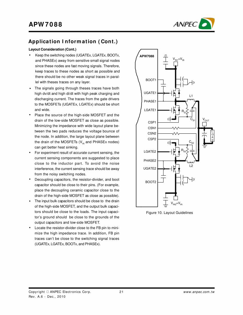
Layout Consideration
In any high switching frequency converter, a correct layout
is important to ensure proper operation of the regulator.
With power devices switching at higher frequency, the
resulting current transient will cause voltage spike across
the interconnecting impedance and parasitic circuit
elements. As an example, consider the turn-off transition
of the PWM MOSFET. Before turn-off condition, the
MOSFET is carrying the full load current. During turn-off,
current stops flowing in the MOSFET and is freewheeling
by the low side MOSFET and parasitic diode. Any parasitic
inductance of the circuit generates a large voltage spike
during the switching interval. In general, using short, wide
printed circuit traces should minimize interconnecting im-
pedances and the magnitude of voltage spike. Besides,
signal and power grounds are to be kept separating and
finally combined using ground plane construction or
single point grounding. The best tie-point between the
signal ground and the power ground is at the negative
side of the output capacitor on each channel, where there
is less noise. Noisy traces beneath the IC are not
recommended. Figure 10. illustrates the layout, with bold
lines indicating high current paths; these traces must be
short and wide. Components along the bold lines should
be placed lose together. Below is a checklist for your
layout :
Copyr ight ANPEC Elect ronics Corp.
Rev. A.6 - Dec. , 2010
APW 7 0 8 8
www.anpec.com.tw21
Applicat ion I nform at ion ( Cont .)
Layout Consideration (Cont.)
The signals going through theses traces have both
high dv/dt and high di/dt with high peak charging and
discharging current. The traces from the gate drivers
to the MOSFETs (UGATEx, LGATEx) should be short
and wide.
Place the source of the high-side MOSFET and the
drain of the low-side MOSFET as close as possible.
Minimizing the impedance with wide layout plane be-
tween the two pads reduces the voltage bounce of
the node. In addition, the large layout plane between
the drain of the MOSFETs (VIN
and PHASEx nodes)
can get better heat sinking.
For experiment result of accurate current sensing, the
current sensing components are suggested to place
close to the inductor part. To avoid the noise
interference, the current sensing trace should be away
from the noisy switching nodes.
Decoupling capacitors, the resistor-divider, and boot
capacitor should be close to their pins. (For example,
place the decoupling ceramic capacitor close to the
drain of the high-side MOSFET as close as possible).
The input bulk capacitors should be close to the drain
of the high-side MOSFET, and the output bulk capaci-
tors should be close to the loads. The input capaci-
tor’s ground should be close to the grounds of the
output capacitors and low-side MOSFET.
Locate the resistor-divider close to the FB pin to mini-
mize the high impedance trace. In addition, FB pin
traces can’t be close to the switching signal traces
(UGATEx, LGATEx, BOOTx, and PHASEx).
•
•
•
•
•
•
Keep the switching nodes (UGATEx, LGATEx, BOOTx,
and PHASEx) away from sensitive small signal nodes
since these nodes are fast moving signals. Therefore,
keep traces to these nodes as short as possible and
there should be no other weak signal traces in paral-
lel with theses traces on any layer.
•
Figure 10. Layout Guidelines
BOOT1
PHASE1
UGATE1
LGATE1
VIN1
=VIN
APW7088
VIN2
=VIN
BOOT2
PHASE2
UGATE2
LGATE2
VOUT
L
OA
D
CS1
CSP1
CSN1
RS1
CSP2
CSN2
RS2
L1
L2
CS2
Copyr ight ANPEC Elect ronics Corp.
Rev. A.6 - Dec. , 2010
APW 7 0 8 8
www.anpec.com.tw22
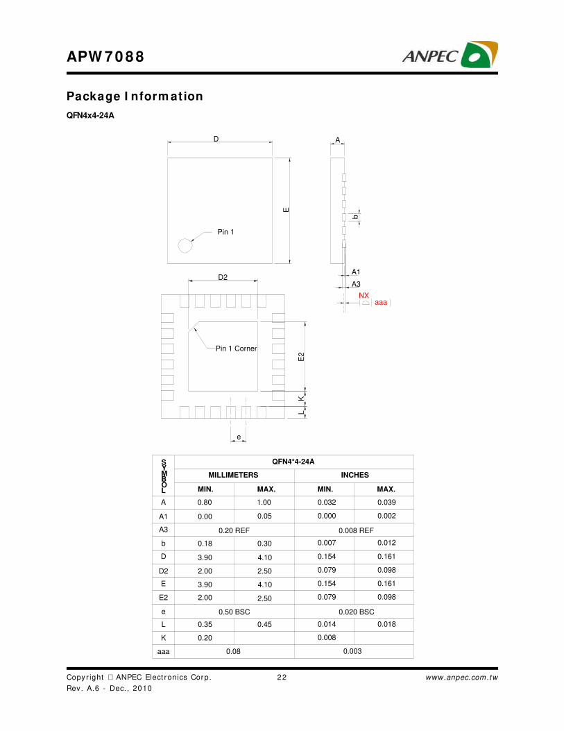
Package I nform ation
QFN4x4-24A
Pin 1
D
E
A
b
A1
A3
NXaaa
Pin 1 Corner
D2
e
E2
KL
0.80
0.098
0.032
0.002
0.50 BSC 0.020 BSC
K 0.20 0.008
3.90 4.10 0.154 0.161
3.90 4.10 0.154 0.161
0.08aaa 0.003
SYMBOL MIN. MAX.
1.00
0.00
0.18 0.30
2.00 2.50
0.05
2.00
A
A1
b
D
D2
E
E2
e
L
MILLIMETERS
A3 0.20 REF
QFN4*4-24A
0.35 0.45
2.50
0.008 REF
MIN. MAX.
INCHES
0.039
0.000
0.007 0.012
0.079 0.098
0.079
0.014 0.018
Copyr ight ANPEC Elect ronics Corp.
Rev. A.6 - Dec. , 2010
APW 7 0 8 8
www.anpec.com.tw23
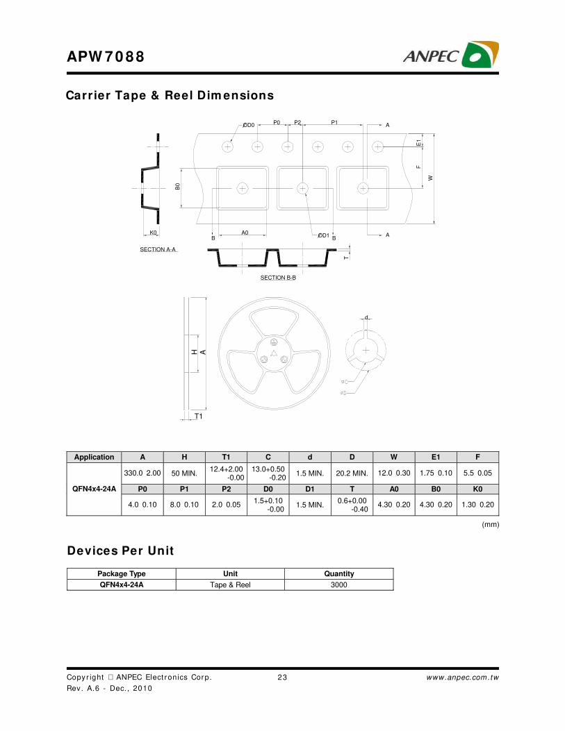
Carrier Tape & Reel Dim ensions
Application A H T1 C d D W E1 F
330.0±2.00 50 MIN. 12.4+2.00 -0.00
13.0+0.50 -0.20
1.5 MIN. 20.2 MIN. 12.0±0.30 1.75±0.10 5.5±0.05
P0 P1 P2 D0 D1 T A0 B0 K0 QFN4x4-24A
4.0±0.10 8.0±0.10 2.0±0.05 1.5+0.10 -0.00
1.5 MIN. 0.6+0.00 -0.40
4.30±0.20 4.30±0.20 1.30±0.20
(mm)
Package Type Unit Quantity
QFN4x4-24A Tape & Reel 3000
Devices Per Unit
A
E1
AB
W
F
T
P0OD0
BA0
P2
K0
B0
SECTION B-B
SECTION A-A
OD1
P1
H
T1
A
d

Copyr ight ANPEC Elect ronics Corp.
Rev. A.6 - Dec. , 2010
APW 7 0 8 8
www.anpec.com.tw24
Taping Direct ion I nform at ion
Classificat ion Profile
QFN4x4-24A
USER DIRECTION OF FEED

Copyr ight ANPEC Elect ronics Corp.
Rev. A.6 - Dec. , 2010
APW 7 0 8 8
www.anpec.com.tw25
Profile Feature Sn-Pb Eutectic Assembly Pb-Free Assembly
Preheat & Soak Temperature min (Tsmin) Temperature max (Tsmax) Time (Tsmin to Tsmax) (ts)
100 °C
150 °C 60-120 seconds
150 °C
200 °C 60-120 seconds
Average ramp-up rate (Tsmax to TP)
3 °C/second max. 3 °C/second max.
Liquidous temperature (TL) Time at liquidous (tL)
183 °C 60-150 seconds
217 °C 60-150 seconds
Peak package body Temperature (Tp)*
See Classification Temp in table 1 See Classification Temp in table 2
Time (tP)** within 5°C of the specified classification temperature (Tc)
20** seconds 30** seconds
Average ramp-down rate (Tp to Tsmax) 6 °C/second max. 6 °C/second max.
Time 25°C to peak temperature 6 minutes max. 8 minutes max.
* Tolerance for peak profile Temperature (Tp) is defined as a supplier minimum and a user maximum. ** Tolerance for time at peak profile temperature (tp) is defined as a supplier minimum and a user maximum.
Table 2. Pb-free Process – Classification Temperatures (Tc)
Package
Thickness
Volume mm3
<350
Volume mm3
350-2000
Volume mm3
>2000
<1.6 mm 260 °C 260 °C 260 °C
1.6 mm – 2.5 mm 260 °C 250 °C 245 °C
≥2.5 mm 250 °C 245 °C 245 °C
Table 1. SnPb Eutectic Process – Classification Temperatures (Tc)
Package
Thickness
Volume mm3
<350
Volume mm3
≥350
<2.5 mm 235 °C 220 °C
≥2.5 mm 220 °C 220 °C
Classificat ion Reflow Profiles
Test item Method Description
SOLDERABILITY JESD-22, B102 5 Sec, 245°C
HOLT JESD-22, A108 1000 Hrs, Bias @ Tj=125°C
PCT JESD-22, A102 168 Hrs, 100%RH, 2atm, 121°C
TCT JESD-22, A104 500 Cycles, -65°C~150°C
HBM MIL-STD-883-3015.7 VHBM≧2KV
MM JESD-22, A115 VMM≧200V
Latch-Up JESD 78 10ms, 1tr≧100mA
Reliability Test Program
Copyr ight ANPEC Elect ronics Corp.
Rev. A.6 - Dec. , 2010
APW 7 0 8 8
www.anpec.com.tw26
Custom er Service
Anpec Electronics Corp.
Head Office :
No.6, Dusing 1st Road, SBIP,
Hsin-Chu, Taiwan, R.O.C.
Tel : 886-3-5642000
Fax : 886-3-5642050
Taipei Branch :
2F, No. 11, Lane 218, Sec 2 Jhongsing Rd.,
Sindian City, Taipei County 23146, Taiwan
Tel : 886-2-2910-3838
Fax : 886-2-2917-3838