
Dual VCO/PLL Synthesizer With IF Up-Converter (Rev. B) Sheets/Texas Instruments PDFs... · •Image...
31
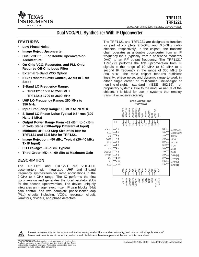
1FEATURES DESCRIPTION LPCC-48 PACKAGE (TOP VIEW) 1 2 3 4 5 6 7 8 9 10 11 12 CP2O LD2 LF2 DATA CLK VCCD2 FR VCCD1 FRBP EN LF1 LD1 13 14 15 16 17 18 19 20 21 22 23 24 CP1O LO1BPA LO1TUN LO1BPB VCCLO1 GND GND GND BBIN BBIP VCCUPC GAIN[0] 36 35 34 33 32 31 30 29 28 27 26 25 EXTLO2IP EXTLO2IN TXON IFOP VCCIF IFON GND GND GAIN[4] GAIN[3] GAIN[2] GAIN[1] 48 47 46 45 44 43 42 41 40 39 38 37 LO2ABPB LO2ATUN LO2ABPA LO2BBPB LO2BTUN LO2BBPA GND LO2OP LO2ON GND VCCLO2 GND TRF1121 TRF1221 SLWS170B–APRIL 2005–REVISED JANUARY 2008 www.ti.com Dual VCO/PLL Synthesizer With IF Upconverter The TRF1121 and TRF1221 are designed to function as part of complete 2.5-GHz and 3.5-GHz radio • Low Phase Noise chipsets, respectively. In the chipset, the transmit • Image Reject Upconverter chain operates as a double upconverter from an IF frequency input (typically from a baseband modem's • Dual VCO/PLL For Double Upconversion DAC) to an RF output frequency. The TRF1121/ Architecture TRF1221 performs the first upconversion from IF • On-Chip VCO, Resonator, and PLL Only; signals in the range of 10 MHz to 60 MHz to a Requires Off-Chip Loop Filter second IF frequency in the range of 300 MHz to • External S-Band VCO Option 360 MHz. The radio chipset features sufficient linearity, phase noise, and dynamic range to work in • 5-Bit Transmit Level Control, 32 dB in 1-dB either single carrier or multicarrier, line-of-sight or Steps non-line-of-sight, standard (IEEE 802.16), or • S-Band LO Frequency Range: proprietary systems. Due to the modular nature of the – TRF1121: 1500 to 2500 MHz chipset, it is ideal for use in systems that employ transmit or receive diversity. – TRF1221: 1700 to 3600 MHz • UHF LO Frequency Range: 250 MHz to 350 MHz • Input Frequency Range: 10 MHz to 70 MHz • S-Band LO Phase Noise Typical 0.5° rms (100 Hz to 1 MHz) • Output Power Range From –32 dBm to 0 dBm in 1-dB Steps (500-mVpp Differential Input) • Minimum UHF LO Step Size of 50 kHz for TRF1121 and 62.5 kHz for TRF1221 • Image Rejection: –50 dBc, Typical (20–40 MHz Tx IF Input) • LO Leakage: –36 dBm, Typical • Third-Order IMD: < –60 dBc at Maximum Gain The TRF1121 and TRF1221 are VHF-UHF upconverters with integrated UHF and S-band frequency synthesizers for radio applications in the 2-GHz to 4-GHz range. The IC performs the first upconversion and generates the local oscillator (LO) for the second upconversion. The device uniquely integrates an image reject mixer, IF gain blocks, 5-bit gain control, and two complete phase-locked-loop (PLL) circuits including: VCOs, resonator circuit, varactors, dividers, and phase detectors. 1 Please be aware that an important notice concerning availability, standard warranty, and use in critical applications of Texas Instruments semiconductor products and disclaimers thereto appears at the end of this data sheet. PRODUCTION DATA information is current as of publication date. Copyright © 2005–2008, Texas Instruments Incorporated Products conform to specifications per the terms of the Texas Instruments standard warranty. Production processing does not necessarily include testing of all parameters.
Transcript of Dual VCO/PLL Synthesizer With IF Up-Converter (Rev. B) Sheets/Texas Instruments PDFs... · •Image...
1FEATURES
DESCRIPTION
LPCC−48 PACKAGE(TOP VIEW)
123
456789
101112
CP2OLD2LF2
DATACLK
VCCD2FR
VCCD1FRBP
ENLF1LD1
13 14 15 16 17 18 19 20 21 22 23 24
CP
1OLO
1BPA
LO1T
UN
LO1B
PB
VC
CLO
1G
ND
GN
DG
ND
BB
IN
BB
IPV
CC
UP
CG
AIN
[0]
363534
333231302928
272625
EXTLO2IPEXTLO2INTXON
IFOPVCCIFIFONGNDGNDGAIN[4]
GAIN[3]GAIN[2]GAIN[1]
48 47 46 45 44 43 42 41 40 39 38 37
LO2A
BP
BLO
2AT
UN
LO2A
BPA
LO2B
BP
BLO
2BT
UN
LO2B
BPA
GN
DLO
2OP
LO2O
N
GN
DV
CC
LO2
GN
D
TRF1121TRF1221
SLWS170B–APRIL 2005–REVISED JANUARY 2008www.ti.com
Dual VCO/PLL Synthesizer With IF UpconverterThe TRF1121 and TRF1221 are designed to functionas part of complete 2.5-GHz and 3.5-GHz radio• Low Phase Noise chipsets, respectively. In the chipset, the transmit
• Image Reject Upconverter chain operates as a double upconverter from an IFfrequency input (typically from a baseband modem's• Dual VCO/PLL For Double UpconversionDAC) to an RF output frequency. The TRF1121/ArchitectureTRF1221 performs the first upconversion from IF• On-Chip VCO, Resonator, and PLL Only; signals in the range of 10 MHz to 60 MHz to aRequires Off-Chip Loop Filter second IF frequency in the range of 300 MHz to
• External S-Band VCO Option 360 MHz. The radio chipset features sufficientlinearity, phase noise, and dynamic range to work in• 5-Bit Transmit Level Control, 32 dB in 1-dBeither single carrier or multicarrier, line-of-sight orStepsnon-line-of-sight, standard (IEEE 802.16), or• S-Band LO Frequency Range: proprietary systems. Due to the modular nature of the
– TRF1121: 1500 to 2500 MHz chipset, it is ideal for use in systems that employtransmit or receive diversity.– TRF1221: 1700 to 3600 MHz
• UHF LO Frequency Range: 250 MHz to350 MHz
• Input Frequency Range: 10 MHz to 70 MHz• S-Band LO Phase Noise Typical 0.5° rms (100
Hz to 1 MHz)• Output Power Range From –32 dBm to 0 dBm
in 1-dB Steps (500-mVpp Differential Input)• Minimum UHF LO Step Size of 50 kHz for
TRF1121 and 62.5 kHz for TRF1221• Image Rejection: –50 dBc, Typical (20–40 MHz
Tx IF Input)• LO Leakage: –36 dBm, Typical• Third-Order IMD: < –60 dBc at Maximum Gain
The TRF1121 and TRF1221 are VHF-UHFupconverters with integrated UHF and S-bandfrequency synthesizers for radio applications in the2-GHz to 4-GHz range. The IC performs the firstupconversion and generates the local oscillator (LO)for the second upconversion. The device uniquelyintegrates an image reject mixer, IF gain blocks, 5-bitgain control, and two complete phase-locked-loop(PLL) circuits including: VCOs, resonator circuit,varactors, dividers, and phase detectors.
1
Please be aware that an important notice concerning availability, standard warranty, and use in critical applications ofTexas Instruments semiconductor products and disclaimers thereto appears at the end of this data sheet.
PRODUCTION DATA information is current as of publication date. Copyright © 2005–2008, Texas Instruments IncorporatedProducts conform to specifications per the terms of the TexasInstruments standard warranty. Production processing does notnecessarily include testing of all parameters.
www.ti.com
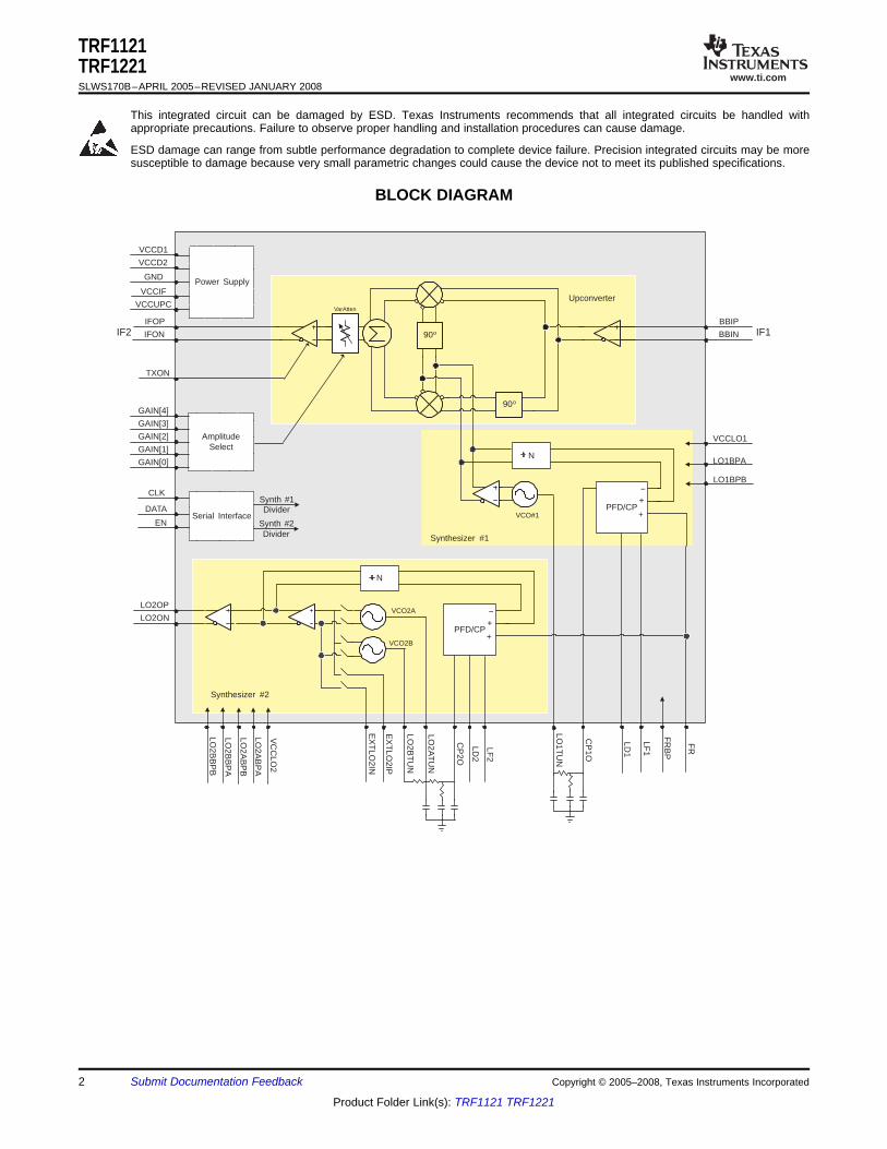
BLOCK DIAGRAM
EX
TLO
2IN
EX
TLO
2IP
LO2B
TU
N
LO2A
TU
N
CP
2O
LD2
LO1T
UN
CP
1O
LD1
FR
BBIP
BBIN
VCCD2
GND
IFOP
IFON
GAIN[3]
CLK
DATA
EN
LO2OP
LO2ON
GAIN[2]
GAIN[1]
GAIN[0]
GAIN[4]
TXON
AmplitudeSelect
Power Supply
Upconverter
90o
90o
Synthesizer #1
N
PFD/CP+
+−
Synthesizer #2
N
PFD/CP+
+−
Serial Interface
Synth #1Divider
Synth #2Divider
VCCIF
VCCUPC
LO2B
BP
A
LO2B
BP
B
LO2A
BP
B
LO2A
BP
A
VC
CLO
2
LF2
LF1
FR
BP
LO1BPB
LO1BPA
VCCLO1
VCCD1
VCO#1
VCO2A
VCO2B
IF1IF2
VarAtten
TRF1121TRF1221SLWS170B–APRIL 2005–REVISED JANUARY 2008
This integrated circuit can be damaged by ESD. Texas Instruments recommends that all integrated circuits be handled withappropriate precautions. Failure to observe proper handling and installation procedures can cause damage.
ESD damage can range from subtle performance degradation to complete device failure. Precision integrated circuits may be moresusceptible to damage because very small parametric changes could cause the device not to meet its published specifications.
2 Submit Documentation Feedback Copyright © 2005–2008, Texas Instruments Incorporated
Product Folder Link(s): TRF1121 TRF1221
www.ti.com
TRF1121TRF1221
SLWS170B–APRIL 2005–REVISED JANUARY 2008
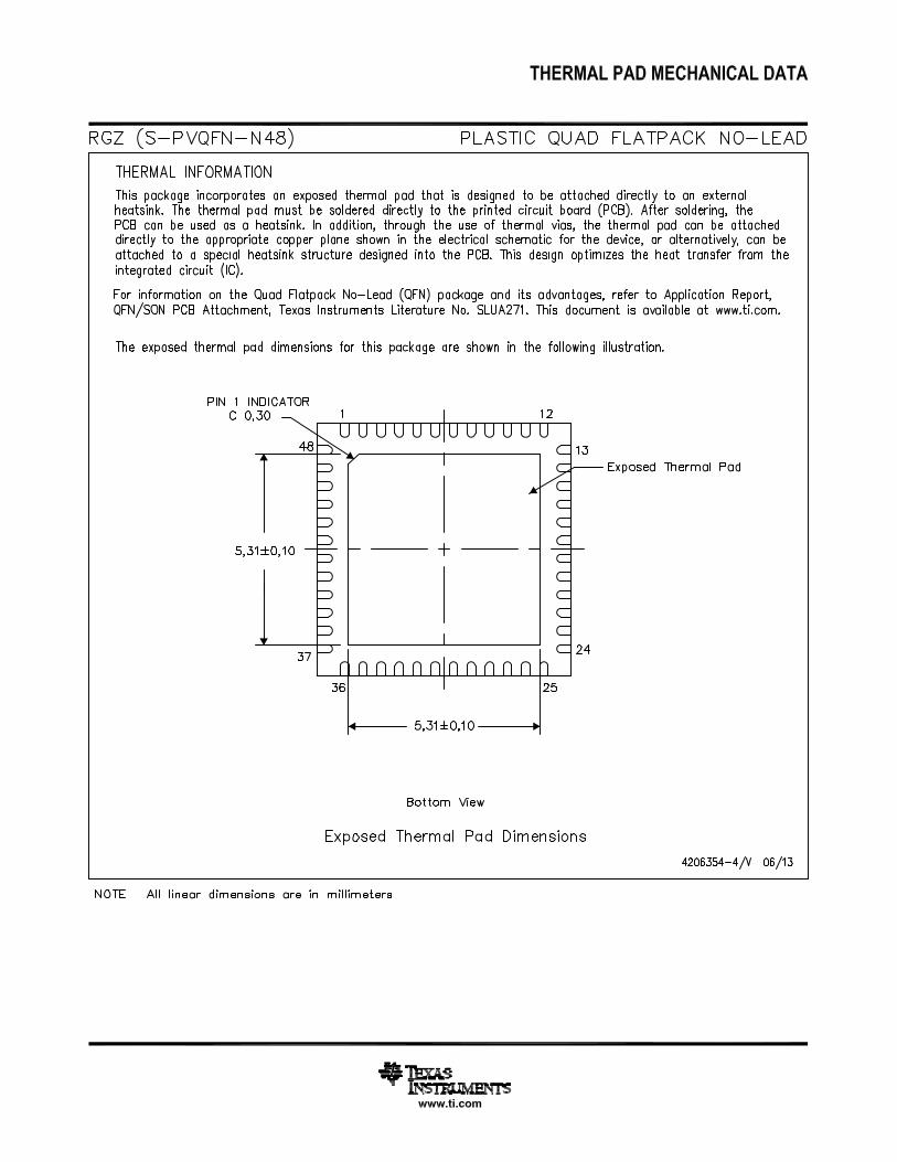
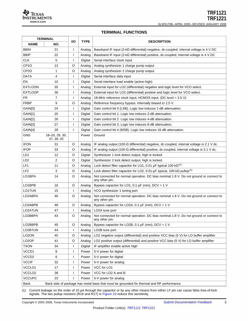
TERMINAL FUNCTIONSTERMINAL
I/O TYPE DESCRIPTIONNAME NO.
BBIN 21 I Analog Baseband IF input (2-kΩ differential) negative, dc-coupled; internal voltage is 4 V DCBBIP 22 I Analog Baseband IF input (2-kΩ differential) positive, dc-coupled; internal voltage is 4 V DCCLK 5 I Digital Serial interface clock inputCP1O 13 O Analog Analog synthesizer 1 charge pump outputCP2O 1 O Analog Analog synthesizer 2 charge pump outputDATA 4 I Digital Serial interface data inputEN 10 I Digital Serial interface load enable (active-high)EXTLO2IN 35 I Analog External input for LO2 (differential) negative and logic level for VCO select.EXTLO2IP 36 I Analog External input for LO2 (differential) positive and logic level for VCO select.FR 7 I Analog 18-MHz reference clock input, HCMOS input. (DC level = 2.5 V)FRBP 9 O Analog Reference frequency bypass. Internally biased to 2.5 V.GAIN[0] 24 I Digital Gain control bit 0 (LSB). Logic low induces 1-dB attenuation.GAIN[1] 25 I Digital Gain control bit 1. Logic low induces 2-dB attenuation.GAIN[2] 26 I Digital Gain control bit 2. Logic low induces 4-dB attenuation.GAIN[3] 27 I Digital Gain control bit 3. Logic low induces 8-dB attenuation.GAIN[4] 28 I Digital Gain control bit 4 (MSB). Logic low induces 16-dB attenuation.GND 18–20, 29, 30, Power Ground
37, 39, 42IFON 31 O Analog IF analog output (100-Ω differential) negative, dc-coupled, internal voltage is 2.1 V dc.IFOP 33 O Analog IF analog output (100-Ω differential) positive, dc-coupled, internal voltage is 2.1 V dc.LD1 12 O Digital Synthesizer 1 lock detect output, high is locked.LD2 2 O Digital Synthesizer 2 lock detect output, high is locked.LF1 11 O Analog Lock detect filter capacitor for LO1, 0.01 µF typical 100 kΩ (1)
LF2 3 O Analog Lock detect filter capacitor for LO2, 0.01-µF typical, 100-kΩ pullup (1)
LO1BPA 14 O Analog Not connected for normal operation. DC bias nominal 1.8 V. Do not ground or connect toany other pin.
LO1BPB 16 O Analog Bypass capacitor for LO1, 0.1 µF (min), DCV = 1 VLO1TUN 15 I Analog VCO synthesizer 1 tuning portLO2ABPA 46 O Analog Not connected for normal operation. DC bias nominal 1.8 V. Do not ground or connect to
any other pin.LO2ABPB 48 O Analog Bypass capacitor for LO2A, 0.1 µF (min), DCV = 1 VLO2ATUN 47 I Analog LO2A tune portLO2BBPA 43 O Analog Not connected for normal operation. DC bias nominal 1.8 V. Do not ground or connect to
any other pin.LO2BBPB 45 O Analog Bypass capacitor for LO2B, 0.1 µF (min), DCV = 1 VLO2BTUN 44 I Analog LO2B tune portLO2ON 40 O Analog LO2 negative output (differential) and positive VCC bias (5 V) for LO buffer amplifierLO2OP 41 O Analog LO2 positive output (differential) and positive VCC bias (5 V) for LO buffer amplifierTXON 34 I Digital IF amplifier enable active highVCCD1 8 I Power 5-V power for digitalVCCD2 6 I Power 5-V power for digitalVCCIF 32 I Power 5-V power for analogVCCLO1 17 I Power VCC for LO1VCCLO2 38 I Power VCC for LO2 A and BVCCUPC 23 I Power 5-V power for analogBack Back side of package has metal base that must be grounded for thermal and RF performance
(1) Current leakage on the order of 10 µA through the capacitor or by any other means from either LF pin can cause false loss-of-locksignals. The two pullup resistors (R16 and R17) in Figure 23 reduce this sensitivity.
Copyright © 2005–2008, Texas Instruments Incorporated Submit Documentation Feedback 3
Product Folder Link(s): TRF1121 TRF1221
www.ti.com
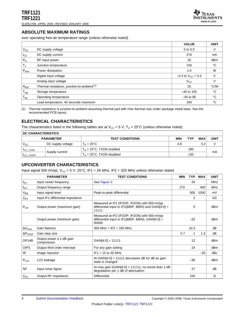
ABSOLUTE MAXIMUM RATINGS
ELECTRICAL CHARACTERISTICS
UPCONVERTER CHARACTERISTICS
TRF1121TRF1221SLWS170B–APRIL 2005–REVISED JANUARY 2008
over operating free-air temperature range (unless otherwise noted)
VALUE UNITVCC DC supply voltage 0 to 5.5 VICC DC supply current 270 mAPin RF input power 20 dBmTJ Junction temperature 150 °CPdiss Power dissipation 1.5 W
Digital input voltage –0.3 to VCC + 0.3 VAnalog input voltage VCC V
RθJC Thermal resistance, junction-to-ambient (1) 25 °C/WTstg Storage temperature –40 to 105 °CTop Operating temperature –40 to 85 °C
Lead temperature, 40 seconds maximum 260 °C
(1) Thermal resistance is junction-to-ambient assuming thermal pad with nine thermal vias under package metal base. See therecommended PCB layout.
The characteristics listed in the following tables are at VCC = 5 V, TA = 25°C (unless otherwise noted)
DC CHARACTERISTICSPARAMETER TEST CONDITIONS MIN TYP MAX UNIT
VCC DC supply voltage TA = 25°C 4.8 5.2 VICC_TxON TA = 25°C, TXON enabled 180
Supply current mAICC_TxOFF TA = 25°C, TXON disabled 130
Input signal 500 mVpp, VCC = 5 V, 25°C, IF1 = 26 MHz, IF2 = 325 MHz unless otherwise stated
PARAMETER TEST CONDITIONS MIN TYP MAX UNITfIF1 Input center frequency See Figure 3 26 MHzfIF2 Output frequency range 270 400 MHzVBB Input signal level Peak-to-peak differential 500 1000 mVZIF1 Input IF1 differential impedance 2 kΩ
Measured at IF2 (IF2OP, IF2ON) with 500-mVppPout Output power (maximum gain) differential input to IF1(BBIP, BBIN) and GAIN[4:0] = 0 dBm
11111Measured at IF2 (IF2OP, IF2ON) with 500-mVpp
Output power (minimum gain) differential input to IF1(BBIP, BBIN), GAIN[4:0] = –32 dBm00000
ΔGmax Gain flatness 300 MHz < IF2 < 330 MHz ±0.3 dBΔPSTEP Gain step size 0.7 1 1.3 dB
Output power a 1-dB gainOP1dB GAIN[4:0] = 11111 12 dBmcompressionOIP3 Output third order intercept For any gain setting 24 dBmIR Image rejection IF1 = 15 to 45 MHz –30 dBc
At GAIN[4:0] = 11111 decreases dB for dB as gainPLO1 LO1 leakage –36 dBmstate is changedAt max gain (GAIN[4:0] = 11111), no worse than 1-dBNF Input noise figure 27 dBdegradation per 1 dB of attenuation
ZIF2 Output RF impedance Differential 100 Ω
4 Submit Documentation Feedback Copyright © 2005–2008, Texas Instruments Incorporated
Product Folder Link(s): TRF1121 TRF1221
www.ti.com
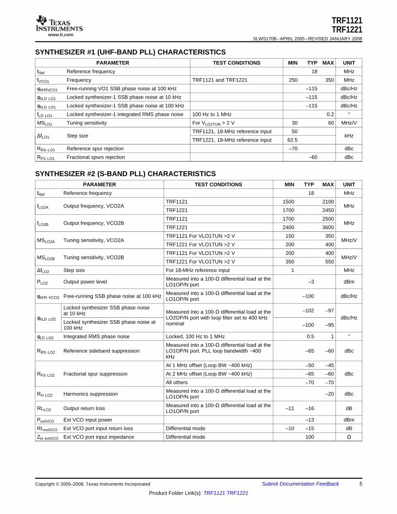
SYNTHESIZER #1 (UHF-BAND PLL) CHARACTERISTICS
SYNTHESIZER #2 (S-BAND PLL) CHARACTERISTICS
TRF1121TRF1221
SLWS170B–APRIL 2005–REVISED JANUARY 2008
PARAMETER TEST CONDITIONS MIN TYP MAX UNITfRef Reference frequency 18 MHzfVCO1 Frequency TRF1121 and TRF1221 250 350 MHzφnFRVCO1 Free-running VO1 SSB phase noise at 100 kHz –115 dBc/HzφnLD LO1 Locked synthesizer-1 SSB phase noise at 10 kHz –115 dBc/HzφnLD LO1 Locked synthesizer-1 SSB phase noise at 100 kHz –115 dBc/HzfLD LO1 Locked synthesizer-1 integrated RMS phase noise 100 Hz to 1 MHz 0.2 °
MSLO1 Tuning sensitivity For VLO1TUN > 2 V 30 60 MHz/VTRF1121, 18-MHz reference input 50
ΔfLO1 Step size kHzTRF1221, 18-MHz reference input 62.5
RRS LO1 Reference spur rejection –70 dBcRFS LO1 Fractional spurs rejection –60 dBc
PARAMETER TEST CONDITIONS MIN TYP MAX UNITfRef Reference frequency 18 MHz
TRF1121 1500 2100fLO2A Output frequency, VCO2A MHz
TRF1221 1700 2450TRF1121 1700 2500
fLO2B Output frequency, VCO2B MHzTRF1221 2400 3600TRF1121 For VLO1TUN >2 V 150 350
MSLO2A Tuning sensitivity, VCO2A MHz/VTRF1221 For VLO1TUN >2 V 200 400TRF1121 For VLO1TUN >2 V 200 400
MSLO2B Tuning sensitivity, VCO2B MHz/VTRF1221 For VLO1TUN >2 V 350 550
ΔfLO2 Step size For 18-MHz reference input 1 MHzMeasured into a 100-Ω differential load at thePLO2 Output power level –3 dBmLO1OP/N portMeasured into a 100-Ω differential load at theφnFR VCO2 Free-running SSB phase noise at 100 kHz –100 dBc/HzLO1OP/N port
Locked synthesizer SSB phase noise –102 –97Measured into a 100-Ω differential load at theat 10 kHzφnLD LO2 LO2OP/N port with loop filter set to 400 kHz dBc/Hz
Locked synthesizer SSB phase noise at nominal –100 –95100 kHzφLD LO2 Integrated RMS phase noise Locked, 100 Hz to 1 MHz 0.5 1 °
Measured into a 100-Ω differential load at theRRS LO2 Reference sideband suppression LO1OP/N port. PLL loop bandwidth ~400 –65 –60 dBc
kHzAt 1 MHz offset (Loop BW ~400 kHz) –50 –45
RFS LO2 Fractional spur suppression At 2 MHz offset (Loop BW ~400 kHz) –65 –60 dBcAll others –70 –70Measured into a 100-Ω differential load at theRH LO2 Harmonics suppression –20 dBcLO1OP/N portMeasured into a 100-Ω differential load at theRLLO2 Output return loss –11 –16 dBLO1OP/N port
PextVCO Ext VCO input power –13 dBmRLextVCO Ext VCO port input return loss Differential mode –10 –15 dBZin extVCO Ext VCO port input impedance Differential mode 100 Ω
Copyright © 2005–2008, Texas Instruments Incorporated Submit Documentation Feedback 5
Product Folder Link(s): TRF1121 TRF1221
www.ti.com
INPUT REFERENCE REQUIREMENTS
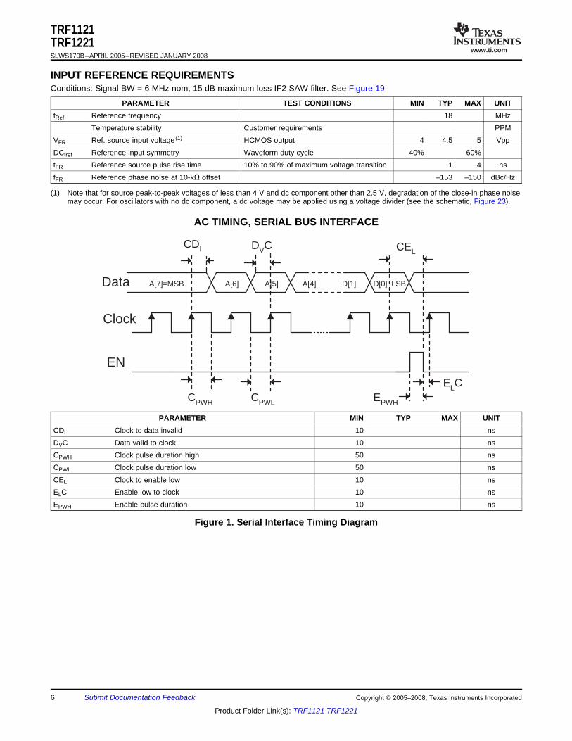
AC TIMING, SERIAL BUS INTERFACE
A[7]=MSB A[6] A[5] D[1]Data
Clock
EN
EPWHCPWLCPWH
D[0] LSBA[4]
CDI DVC CEL
ELC
TRF1121TRF1221SLWS170B–APRIL 2005–REVISED JANUARY 2008
Conditions: Signal BW = 6 MHz nom, 15 dB maximum loss IF2 SAW filter. See Figure 19
PARAMETER TEST CONDITIONS MIN TYP MAX UNITfRef Reference frequency 18 MHz
Temperature stability Customer requirements PPMVFR Ref. source input voltage (1) HCMOS output 4 4.5 5 VppDCfref Reference input symmetry Waveform duty cycle 40% 60%tFR Reference source pulse rise time 10% to 90% of maximum voltage transition 1 4 nsfFR Reference phase noise at 10-kΩ offset –153 –150 dBc/Hz
(1) Note that for source peak-to-peak voltages of less than 4 V and dc component other than 2.5 V, degradation of the close-in phase noisemay occur. For oscillators with no dc component, a dc voltage may be applied using a voltage divider (see the schematic, Figure 23).
PARAMETER MIN TYP MAX UNITCDI Clock to data invalid 10 nsDVC Data valid to clock 10 nsCPWH Clock pulse duration high 50 nsCPWL Clock pulse duration low 50 nsCEL Clock to enable low 10 nsELC Enable low to clock 10 nsEPWH Enable pulse duration 10 ns
Figure 1. Serial Interface Timing Diagram
6 Submit Documentation Feedback Copyright © 2005–2008, Texas Instruments Incorporated
Product Folder Link(s): TRF1121 TRF1221
www.ti.com
DIGITAL INTERFACE CHARACTERISTICS
AUXILIARY AND CONTROL
TRF1121TRF1221
SLWS170B–APRIL 2005–REVISED JANUARY 2008
Conditions: Signal BW = 6 MHz nom, 15 dB maximum loss IF2 SAW filter. See Figure 19
PARAMETER TEST CONDITIONS MIN TYP MAX UNITVIH Input high voltage 2.1 5 VVIL Input low voltage 0 0.8 VIIH Input high current 0 50 µAIIL Input low current 0 –50 µACI Input capacitance 3 pFVOH Output logic 1 voltage 0 to 100-µA load 2.4 3.6 VROH Output logic 1 impedance 18 kΩVOL Output low voltage 0 to –100-µA load 0 0.4 V
PARAMETER TEST CONDITIONS MIN TYP MAX UNITIF output on High
TXON IF amplifier enableIF output off Low
EXTLO2IP HighOn-chip VCO2A selection Logic level applied to EXTLOIP and EXTLOIN pins toEXTLO2IN Low
select either on chip VCO 2A or 2B. Pullup resistor = 200 ΩEXTLO2IP Lowand pulldown resistor = 1 kΩ.On-chip VCO2B selectionEXTLO2IN HighEXTLO2IP LowLogic level applied to EXTLOIP and EXTLOIN pins toOn-chip VCO2 selection select the external VCO2 inputEXTLO2IN Low
Copyright © 2005–2008, Texas Instruments Incorporated Submit Documentation Feedback 7
Product Folder Link(s): TRF1121 TRF1221
www.ti.com
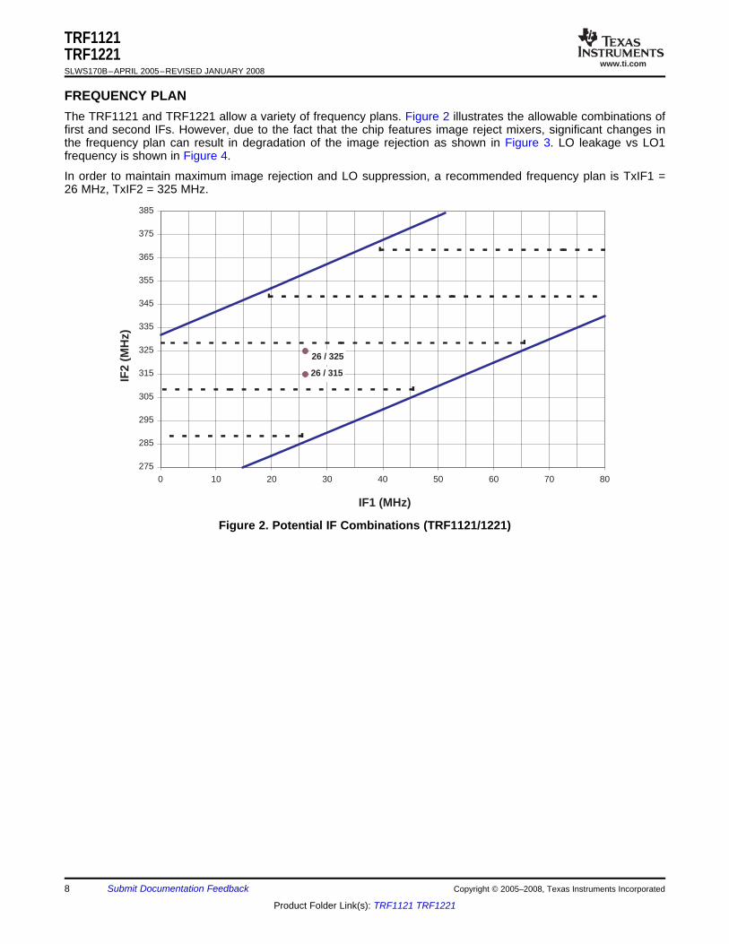
FREQUENCY PLAN
26 / 315
26 / 325
275
285
295
305
315
325
335
345
355
365
375
385
0 10 20 30 40 50 60 70 80
IF1 (MHz)
IF2
(MH
z)
TRF1121TRF1221SLWS170B–APRIL 2005–REVISED JANUARY 2008
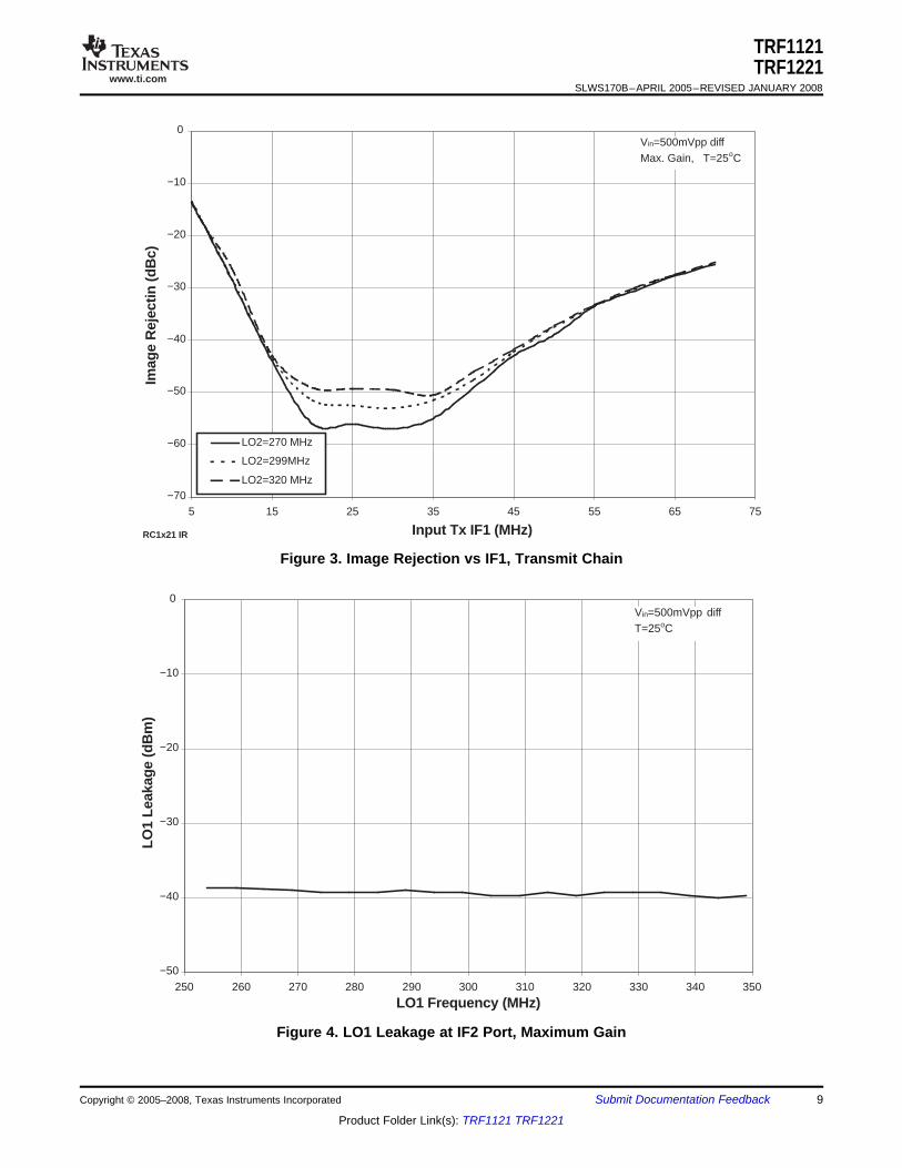
The TRF1121 and TRF1221 allow a variety of frequency plans. Figure 2 illustrates the allowable combinations offirst and second IFs. However, due to the fact that the chip features image reject mixers, significant changes inthe frequency plan can result in degradation of the image rejection as shown in Figure 3. LO leakage vs LO1frequency is shown in Figure 4.
In order to maintain maximum image rejection and LO suppression, a recommended frequency plan is TxIF1 =26 MHz, TxIF2 = 325 MHz.
Figure 2. Potential IF Combinations (TRF1121/1221)
8 Submit Documentation Feedback Copyright © 2005–2008, Texas Instruments Incorporated
Product Folder Link(s): TRF1121 TRF1221
www.ti.com
RC1x21 IR
−70
−60
−50
−40
−30
−20
−10
0
5 15 25 35 45 55 65 75
Input Tx IF1 (MHz)
Imag
e R
ejec
tin (d
Bc)
LO2=270 MHz
LO2=299MHz
LO2=320 MHz
Vin=500mVpp diffMax. Gain, T=25oC
−50
−40
−30
−20
−10
0
250 260 270 280 290 300 310 320 330 340 350
LO1 Frequency (MHz)
LO
1 L
eaka
ge
(dB
m)
Vin=500mVpp diffT=25oC
TRF1121TRF1221
SLWS170B–APRIL 2005–REVISED JANUARY 2008
Figure 3. Image Rejection vs IF1, Transmit Chain
Figure 4. LO1 Leakage at IF2 Port, Maximum Gain
Copyright © 2005–2008, Texas Instruments Incorporated Submit Documentation Feedback 9
Product Folder Link(s): TRF1121 TRF1221
www.ti.com
TRANSMIT LEVEL CONTROL
RC1x21 Po, PLO, IM3 (G)
−3
−2
−1
0
1
024681012141618202224262830Gain State
Gai
n D
evia
tio
n f
rom
Idea
l (d
B)
−80
−70
−60
−50
−40
−30
−20
−10
0
Pout
Po
ut,
LO
Lea
kag
e (d
Bm
) IM
D L
evel
(d
Bc)
LO1 Leakageat IF2 port
Gain Deviationfrom ideal
IMD Level with two input tones at 250 mVpp diff. each
Vin=500mVpp diffT=25oC
TRF1121TRF1221SLWS170B–APRIL 2005–REVISED JANUARY 2008
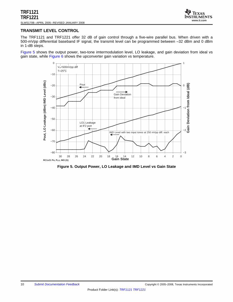
The TRF1121 and TRF1221 offer 32 dB of gain control through a five-wire parallel bus. When driven with a500-mVpp differential baseband IF signal, the transmit level can be programmed between –32 dBm and 0 dBmin 1-dB steps.
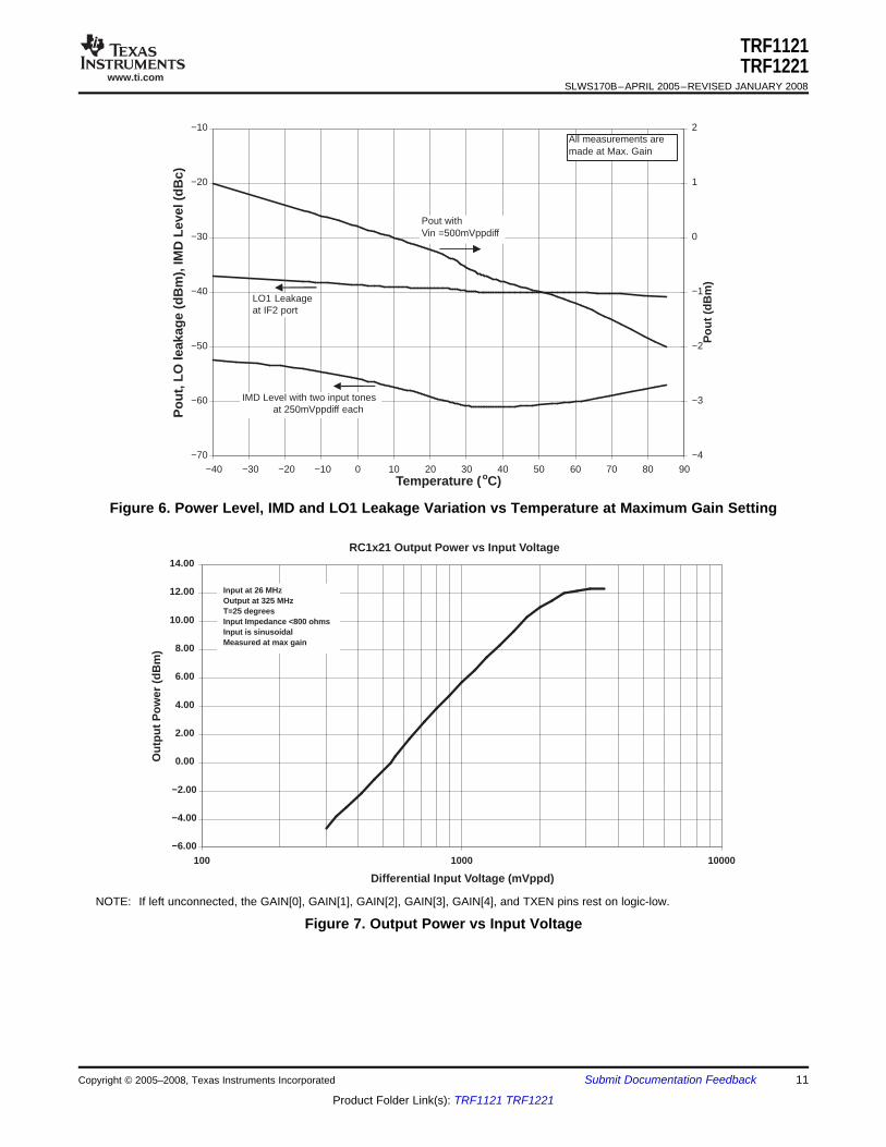
Figure 5 shows the output power, two-tone imtermodulation level, LO leakage, and gain deviation from ideal vsgain state, while Figure 6 shows the upconverter gain variation vs temperature.
Figure 5. Output Power, LO Leakage and IMD Level vs Gain State
10 Submit Documentation Feedback Copyright © 2005–2008, Texas Instruments Incorporated
Product Folder Link(s): TRF1121 TRF1221
www.ti.com
−70
−60
−50
−40
−30
−20
−10
−40 −30 −20 −10 0 10 20 30 40 50 60 70 80 90Temperature (oC)
Po
ut,
LO
leak
age
(dB
m),
IMD
Lev
el (
dB
c)
−4
−3
−2
−1
0
1
2
Pout withVin =500mVppdiff
LO1 Leakageat IF2 port
IMD Level with two input tones at 250mVppdiff each
Po
ut
(dB
m)
All measurements aremade at Max. Gain
RC1x21 Output Power vs Input V oltage
−6.00
−4.00
−2.00
0.00
2.00
4.00
6.00
8.00
10.00
12.00
14.00
100 1000 10000
Differential Input V oltage (mVppd)
Out
put P
ower
(dB
m)
Input at 26 MHzOutput at 325 MHzT=25 degreesInput Impedance <800 ohmsInput is sinusoidalMeasured at max gain
TRF1121TRF1221
SLWS170B–APRIL 2005–REVISED JANUARY 2008
Figure 6. Power Level, IMD and LO1 Leakage Variation vs Temperature at Maximum Gain Setting
NOTE: If left unconnected, the GAIN[0], GAIN[1], GAIN[2], GAIN[3], GAIN[4], and TXEN pins rest on logic-low.
Figure 7. Output Power vs Input Voltage
Copyright © 2005–2008, Texas Instruments Incorporated Submit Documentation Feedback 11
Product Folder Link(s): TRF1121 TRF1221
www.ti.com
INTEGRATED SYNTHESIZERS
PLL Programming
out
Ff REFIN 8 (N 3) S 2 M
18
é ù= ´ ´ + - - ¸ ´é ùë ûê ú
ë û (1)
TRF1121TRF1221SLWS170B–APRIL 2005–REVISED JANUARY 2008
Synthesizer #1 (UHF) and synthesizer #2 (S-band) are both integrated in the TRF1121/TRF1221. These twoPLLs can be programmed via a 3-wire serial bus (CLK, DATA, and EN) from the baseband processor. The timingspecifications are given in the ac timing table.
Synthesizer #2 has a step size of 1 MHz, while Synthesizer #1 offers a step size of 50 kHz, both assuming an18-MHz reference frequency. Different reference frequencies yield different step sizes, many of which may benon-integer.
NOTE:
If left unconnected, the DATA, CLK and EN pins rest on logic-high. EN islevel-sensitive.
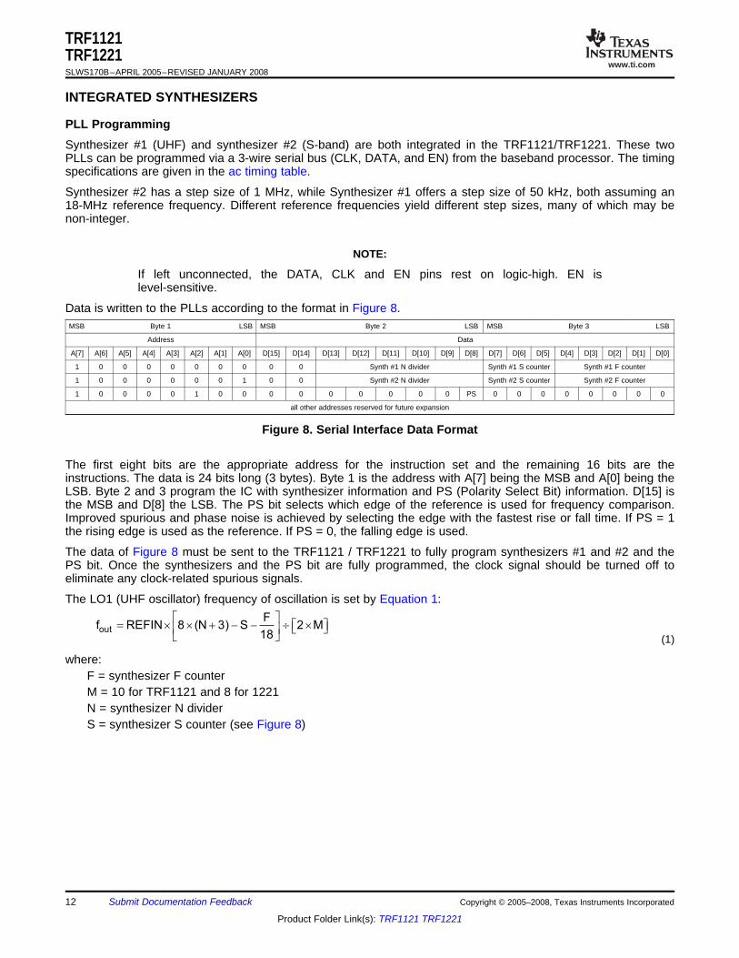
Data is written to the PLLs according to the format in Figure 8.MSB Byte 1 LSB MSB Byte 2 LSB MSB Byte 3 LSB
Address Data
A[7] A[6] A[5] A[4] A[3] A[2] A[1] A[0] D[15] D[14] D[13] D[12] D[11] D[10] D[9] D[8] D[7] D[6] D[5] D[4] D[3] D[2] D[1] D[0]
1 0 0 0 0 0 0 0 0 0 Synth #1 N divider Synth #1 S counter Synth #1 F counter
1 0 0 0 0 0 0 1 0 0 Synth #2 N divider Synth #2 S counter Synth #2 F counter
1 0 0 0 0 1 0 0 0 0 0 0 0 0 0 PS 0 0 0 0 0 0 0 0
all other addresses reserved for future expansion
Figure 8. Serial Interface Data Format
The first eight bits are the appropriate address for the instruction set and the remaining 16 bits are theinstructions. The data is 24 bits long (3 bytes). Byte 1 is the address with A[7] being the MSB and A[0] being theLSB. Byte 2 and 3 program the IC with synthesizer information and PS (Polarity Select Bit) information. D[15] isthe MSB and D[8] the LSB. The PS bit selects which edge of the reference is used for frequency comparison.Improved spurious and phase noise is achieved by selecting the edge with the fastest rise or fall time. If PS = 1the rising edge is used as the reference. If PS = 0, the falling edge is used.
The data of Figure 8 must be sent to the TRF1121 / TRF1221 to fully program synthesizers #1 and #2 and thePS bit. Once the synthesizers and the PS bit are fully programmed, the clock signal should be turned off toeliminate any clock-related spurious signals.
The LO1 (UHF oscillator) frequency of oscillation is set by Equation 1:
where:F = synthesizer F counterM = 10 for TRF1121 and 8 for 1221N = synthesizer N dividerS = synthesizer S counter (see Figure 8)
12 Submit Documentation Feedback Copyright © 2005–2008, Texas Instruments Incorporated
Product Folder Link(s): TRF1121 TRF1221
www.ti.com
out
Ff REFIN 8 (N 3) S
18
é ù= ´ ´ + - -ê ú
ë û (2)
TRF1121TRF1221
SLWS170B–APRIL 2005–REVISED JANUARY 2008
The TRF1121/TRF1221 contains two independent S-band VCOs and resonator circuits to provide additionalfrequency range from one IC, however only one VCO can be enabled at a time. These two VCOs are referred toas VCO2A and VCO2B (see the block diagram). The S-band PLL (LO2A or LO2B) frequency of oscillation is setby the following equation:
where:F = synthesizer F counterN = synthesizer N dividerS = synthesizer S counter (see Figure 8)
F has a range of 0 to 17. Both N and S have ranges that are limited more by the LO range than by their digitalcount.
Both synthesizers have a fractional architecture, which allows a high comparison frequency relative to the stepsize. The S-band PLL operates at a reference frequency of 18 MHz with a minimum phase accumulatorfrequency of 1 MHz. The UHF PLL operates at a 9-MHz reference with a minimum phase accumulator frequencyof 0.5 MHz. The S-band PLL has a step size of 1 MHz and the UHF PLL has a step size of 50 kHz (TRF1121) or62.5 kHz (TRF1221), when using an 18-MHz reference frequency. Different reference frequencies yield differentstep sizes, many of which are non-integer. If a different reference frequency is chosen, the step size is linearlyrelated to the step size for 18 MHz.
Step size = step size at 18 MHz × [REF FREQ / 18 MHz]
In addition to the normal reference spurious signals at the comparison frequency, fractional synthesizers havefractional spurs. The fractional spurs occur at an offset from the LO signal that is dependent on the differencebetween the LO frequency and integer multiples of the reference frequency. They occur on both sides of the LOcarrier. The spur locations can be found by the following process: divide the LO frequency by the referencefrequency, take the remainder (fraction to the right of the whole number) and multiply it by the referencefrequency. This frequency is the difference between the actual LO frequency and an integer-multiple of thereference frequency. Fractional spurs occur at this frequency and the reference frequency minus this frequency.
The following example best explains the process: if LO2 is set to 2206 MHz when using an 18-MHz referencefrequency, then 2206/18 is 122.55556. The difference between the LO and 122 × 18 MHz is:
0.55556 × 18 MHz = 10 MHz
The fractional spurs occur at this frequency offset (10 MHz) from LO2 and:18–10 MHz or 8 MHz offset from LO2.
The fractional spurious level varies with the offset from the LO because the spurs are attenuated by the loop filterresponse. The larger the offset from the LO, the lower the spur level. In general, spurs at offsets greater than3 MHz or 4 MHz are below –75 dBc and are not a concern. The worst fractional spur levels occur when they arelocated at 1-MHz offsets from the LO2. (Note: the fractional spurs are offset from the LO2 by 1 MHz when thedifference between the LO2 and an integer multiple of the reference frequency is 1 MHz or 17 MHz).
Although both synthesizers have fractional spurs, for most applications the spurious signals from the UHFsynthesizer can be ignored because the LO1 spurs are filtered by the IF2 filter and attenuated by frequencydividers that are located after the LO1 generation. In some frequency plans it is possible to offset LO1 and LO2to avoid worst case fractional spurs (at 1-MHz offsets) on LO2.
Copyright © 2005–2008, Texas Instruments Incorporated Submit Documentation Feedback 13
Product Folder Link(s): TRF1121 TRF1221
www.ti.com
VCO Tuning Characteristics
1000
1250
1500
1750
2000
2250
2500
1 1.5 2 2.5 3 3.5 4 4.5 5
Tuning Voltage (V)
Fre
qu
ency
(MH
z)
100
200
300
400
500
600
700
Mo
d S
ense
(MH
z/V
)
Mod Sense
Frequency
−40 ºC+25 ºC+85 ºC
1250
1500
1750
2000
2250
2500
2750
1 1.5 2 2.5 3 3.5 4 4.5 5
Tuning V oltage (V)
Fre
quen
cy (
MH
z)
100
200
300
400
500
600
700
Mod
Sen
se (
MH
z/V
)
Mod Sense
Frequency
−40 ºC+25 ºC+85 ºC
TRF1121TRF1221SLWS170B–APRIL 2005–REVISED JANUARY 2008
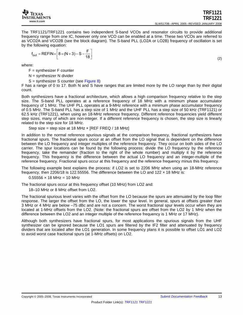
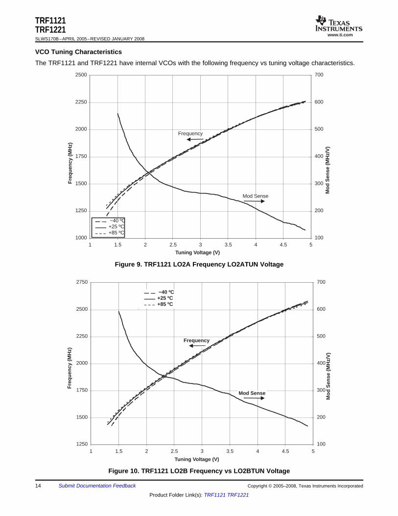
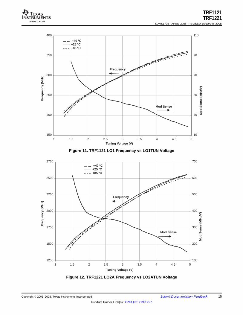
The TRF1121 and TRF1221 have internal VCOs with the following frequency vs tuning voltage characteristics.
Figure 9. TRF1121 LO2A Frequency LO2ATUN Voltage
Figure 10. TRF1121 LO2B Frequency vs LO2BTUN Voltage
14 Submit Documentation Feedback Copyright © 2005–2008, Texas Instruments Incorporated
Product Folder Link(s): TRF1121 TRF1221
www.ti.com
150
200
250
300
350
400
1 1.5 2 2.5 3 3.5 4 4.5 5Tuning V oltage (V)
Fre
quen
cy (
MH
z)
10
30
50
70
90
110
Mod
Sen
se (
MH
z/V
)
Mod Sense
Frequency
−40 ºC+25 ºC+85 ºC
1250
1500
1750
2000
2250
2500
2750
1 1.5 2 2.5 3 3.5 4 4.5 5
Tuning V oltage (V)
Fre
quen
cy (
MH
z)
100
200
300
400
500
600
700
Mod
Sen
se (
MH
z/V
)
Mod Sense
Frequency
−40 ºC+25 ºC+85 ºC
TRF1121TRF1221
SLWS170B–APRIL 2005–REVISED JANUARY 2008
Figure 11. TRF1121 LO1 Frequency vs LO1TUN Voltage
Figure 12. TRF1221 LO2A Frequency vs LO2ATUN Voltage
Copyright © 2005–2008, Texas Instruments Incorporated Submit Documentation Feedback 15
Product Folder Link(s): TRF1121 TRF1221
www.ti.com
2000
2250
2500
2750
3000
3250
3500
3750
4000
1 1.5 2 2.5 3 3.5 4 4.5 5
Tuning V oltage (V)
Fre
quen
cy (
MH
z)
100
200
300
400
500
600
700
800
900
Mod
Sen
se (
MH
z/V
)
Mod Sense
Frequency
−40 ºC+25 ºC+85 ºC
−40C 25C 85C
400 110
350
300
250
200
150
90
70
50
30
10
Frequency
Mod Sense
Fre
quen
cy −
MH
z
Mod
Sen
se −
MH
z/V
Tuning V oltage − V
1 1.5 2 2.5 3 3.5 4 4.5 5
TRF1121TRF1221SLWS170B–APRIL 2005–REVISED JANUARY 2008
Figure 13. TRF1221 LO2B Frequency vs LO2BTUN Voltage
Figure 14. TRF1221 LO1 Frequency vs LO1TUN Voltage
16 Submit Documentation Feedback Copyright © 2005–2008, Texas Instruments Incorporated
Product Folder Link(s): TRF1121 TRF1221
www.ti.com
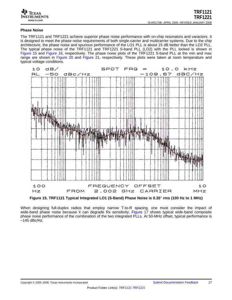
Phase Noise
TRF1121TRF1221
SLWS170B–APRIL 2005–REVISED JANUARY 2008
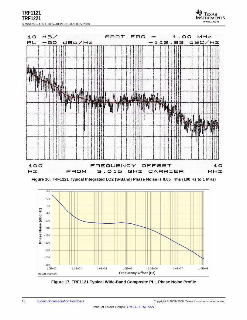
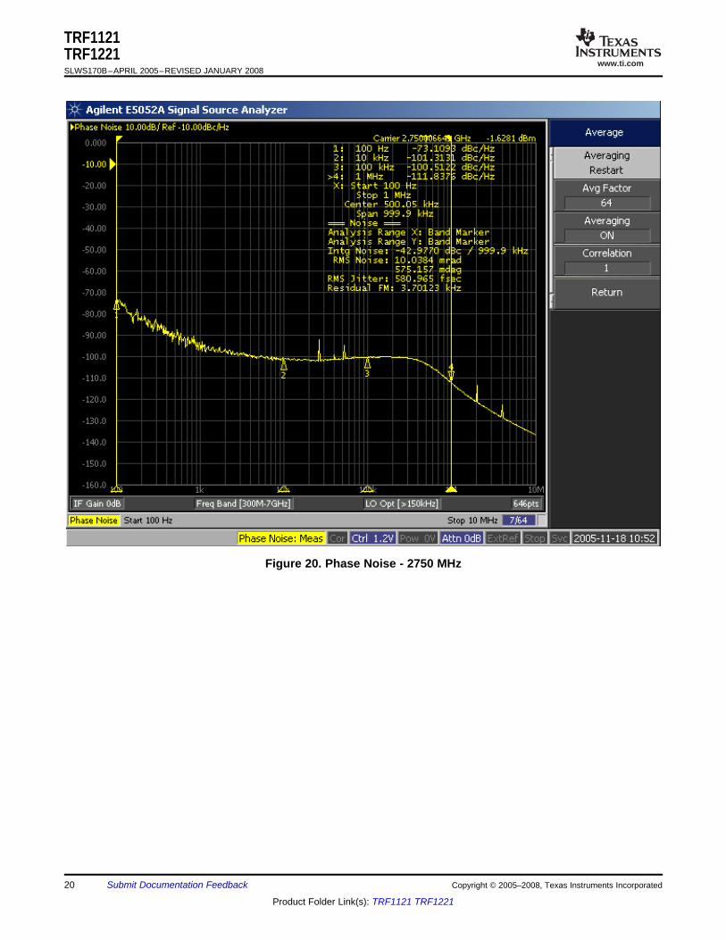
The TRF1121 and TRF1221 achieve superior phase noise performance with on-chip resonators and varactors. Itis designed to meet the phase noise requirements of both single-carrier and multicarrier systems. Due to the chiparchitecture, the phase noise and spurious performance of the LO1 PLL is about 15 dB better than the LO2 PLL.The typical phase noise of the TRF1121 and TRF1221 S-band PLL (LO2) with the PLL locked is shown inFigure 15 and Figure 16, respectively. The phase noise plots of the TRF1221 S-band PLL at the min and maxrange are shown in Figure 20 and Figure 21, respectively. These plots were taken at room temperature andtypical voltage conditions.
Figure 15. TRF1121 Typical Integrated LO1 (S-Band) Phase Noise is 0.35° rms (100 Hz to 1 MHz)
When designing full-duplex radios that employ narrow T-to-R spacing, one must consider the impact ofwide-band phase noise because it can degrade Rx sensitivity. Figure 17 shows typical wide-band compositephase noise performance of the combination of the two integrated PLLs. At 50-MHz offset, typical performance is–145 dBc/Hz.
Copyright © 2005–2008, Texas Instruments Incorporated Submit Documentation Feedback 17
Product Folder Link(s): TRF1121 TRF1221
www.ti.com
RC1121 cmpPhsNs
−160
−150
−140
−130
−120
−110
−100
−90
−80
−70
−60
1.0E+02 1.0E+03 1.0E+04 1.0E+05 1.0E+06 1.0E+07 1.0E+08
Frequency Offset (Hz)
Ph
ase
No
ise
(dB
c/H
z)
TRF1121TRF1221SLWS170B–APRIL 2005–REVISED JANUARY 2008
Figure 16. TRF1221 Typical Integrated LO2 (S-Band) Phase Noise is 0.65° rms (100 Hz to 1 MHz)
Figure 17. TRF1121 Typical Wide-Band Composite PLL Phase Noise Profile
18 Submit Documentation Feedback Copyright © 2005–2008, Texas Instruments Incorporated
Product Folder Link(s): TRF1121 TRF1221
www.ti.com
TRF1121TRF1221
SLWS170B–APRIL 2005–REVISED JANUARY 2008
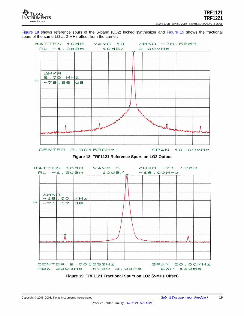
Figure 18 shows reference spurs of the S-band (LO2) locked synthesizer and Figure 19 shows the fractionalspurs of the same LO at 2-MHz offset from the carrier.
Figure 18. TRF1121 Reference Spurs on LO2 Output
Figure 19. TRF1121 Fractional Spurs on LO2 (2-MHz Offset)
Copyright © 2005–2008, Texas Instruments Incorporated Submit Documentation Feedback 19
Product Folder Link(s): TRF1121 TRF1221
www.ti.com
TRF1121TRF1221SLWS170B–APRIL 2005–REVISED JANUARY 2008
Figure 20. Phase Noise - 2750 MHz
20 Submit Documentation Feedback Copyright © 2005–2008, Texas Instruments Incorporated
Product Folder Link(s): TRF1121 TRF1221
www.ti.com
TRF1121TRF1221
SLWS170B–APRIL 2005–REVISED JANUARY 2008
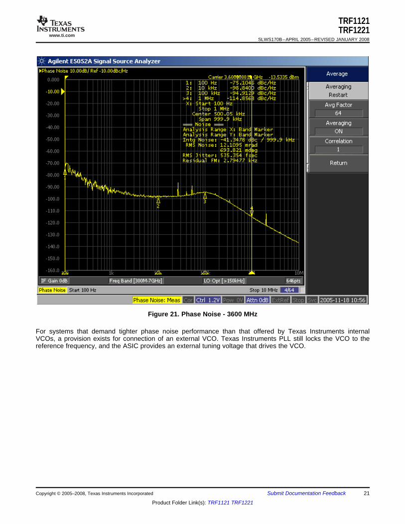
Figure 21. Phase Noise - 3600 MHz
For systems that demand tighter phase noise performance than that offered by Texas Instruments internalVCOs, a provision exists for connection of an external VCO. Texas Instruments PLL still locks the VCO to thereference frequency, and the ASIC provides an external tuning voltage that drives the VCO.
Copyright © 2005–2008, Texas Instruments Incorporated Submit Documentation Feedback 21
Product Folder Link(s): TRF1121 TRF1221
www.ti.com
APPLICATION INFORMATION
Dia. 15 Mil(0,381 mm) 1 oz. (0,035 mm) Copper + ½ oz. (0,018 mm)
Copper Plated Upper and Lower Surfaces
Layer 2: 1 oz. (0,035 mm) Copper
Layer 3: 1 oz. (0,035 mm) Copper
½ oz. (0,018 mm) Copper Plated
DuPont CB 100Conductive ViaPlug
8 Mil(0,203 mm)
Prepreg
35 Mil(0,889 mm)
Layer 4
Layer 1
M0020-03
10 Mil (0,254 mm)Core FR4
10 Mil (0,254 mm)Core FR4
TRF1121TRF1221SLWS170B–APRIL 2005–REVISED JANUARY 2008
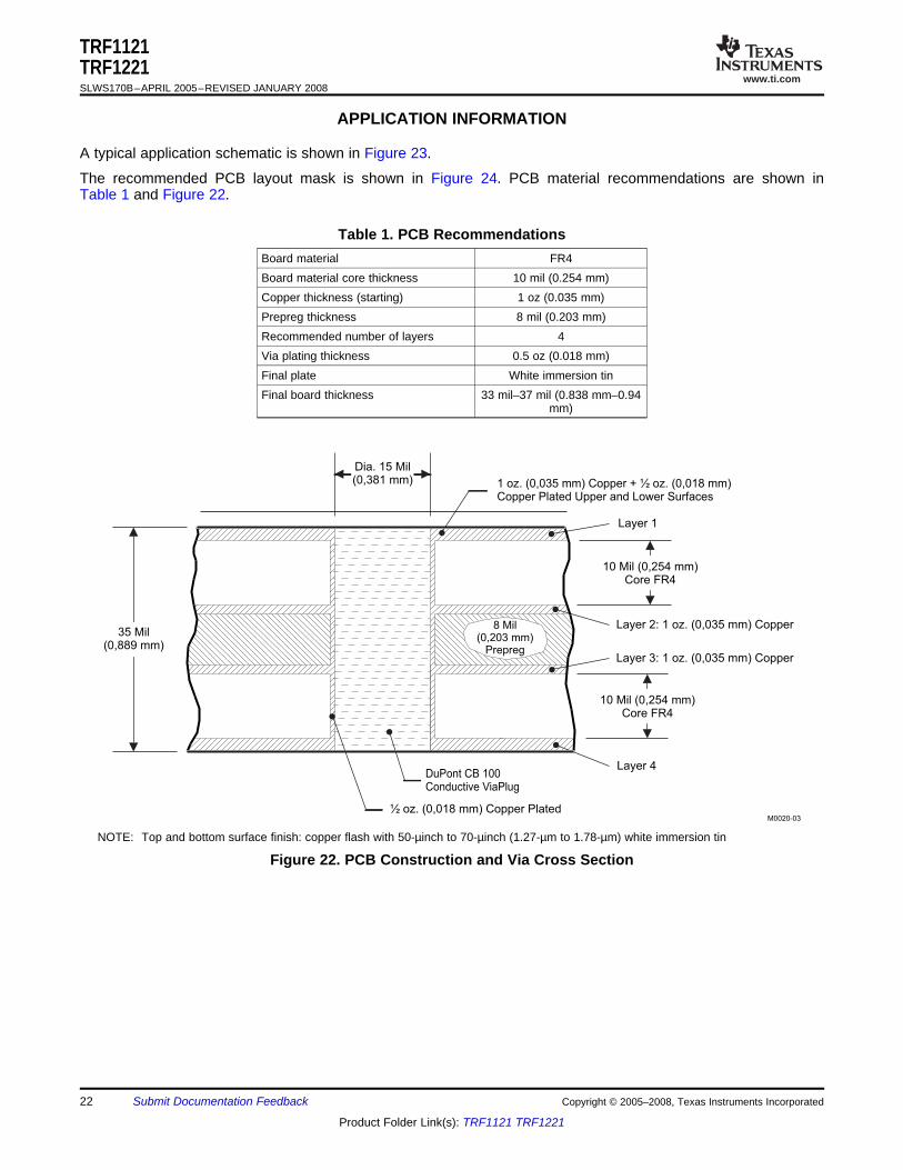
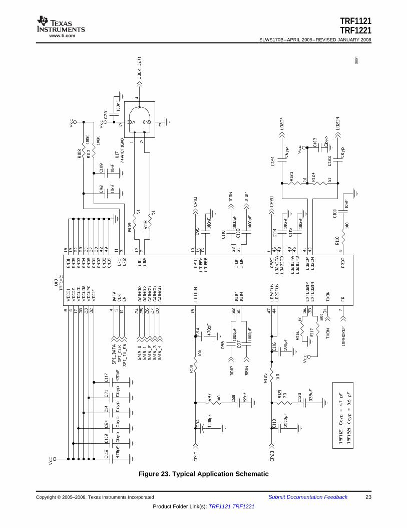
A typical application schematic is shown in Figure 23.
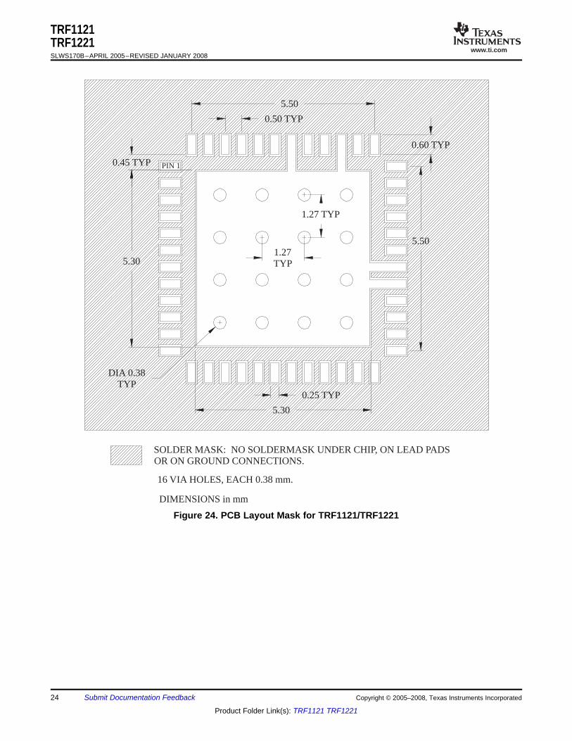
The recommended PCB layout mask is shown in Figure 24. PCB material recommendations are shown inTable 1 and Figure 22.
Table 1. PCB RecommendationsBoard material FR4Board material core thickness 10 mil (0.254 mm)Copper thickness (starting) 1 oz (0.035 mm)Prepreg thickness 8 mil (0.203 mm)Recommended number of layers 4Via plating thickness 0.5 oz (0.018 mm)Final plate White immersion tinFinal board thickness 33 mil–37 mil (0.838 mm–0.94
mm)
NOTE: Top and bottom surface finish: copper flash with 50-µinch to 70-µinch (1.27-µm to 1.78-µm) white immersion tin
Figure 22. PCB Construction and Via Cross Section
22 Submit Documentation Feedback Copyright © 2005–2008, Texas Instruments Incorporated
Product Folder Link(s): TRF1121 TRF1221
www.ti.com
S0
01
TRF1121TRF1221
SLWS170B–APRIL 2005–REVISED JANUARY 2008
Figure 23. Typical Application Schematic
Copyright © 2005–2008, Texas Instruments Incorporated Submit Documentation Feedback 23
Product Folder Link(s): TRF1121 TRF1221
www.ti.com
DIMENSIONS in mm
16 VIA HOLES, EACH 0.38 mm.
SOLDER MASK: NO SOLDERMASK UNDER CHIP, ON LEAD PADSOR ON GROUND CONNECTIONS.
1.27 TYP
1.27TYP
0.60 TYP
5.50
0.50 TYP
0.45 TYP
5.30
5.30
5.50
DIA 0.38TYP
0.25 TYP
PIN 1
TRF1121TRF1221SLWS170B–APRIL 2005–REVISED JANUARY 2008
Figure 24. PCB Layout Mask for TRF1121/TRF1221
24 Submit Documentation Feedback Copyright © 2005–2008, Texas Instruments Incorporated
Product Folder Link(s): TRF1121 TRF1221
PACKAGE OPTION ADDENDUM
www.ti.com 9-Aug-2013
Addendum-Page 1
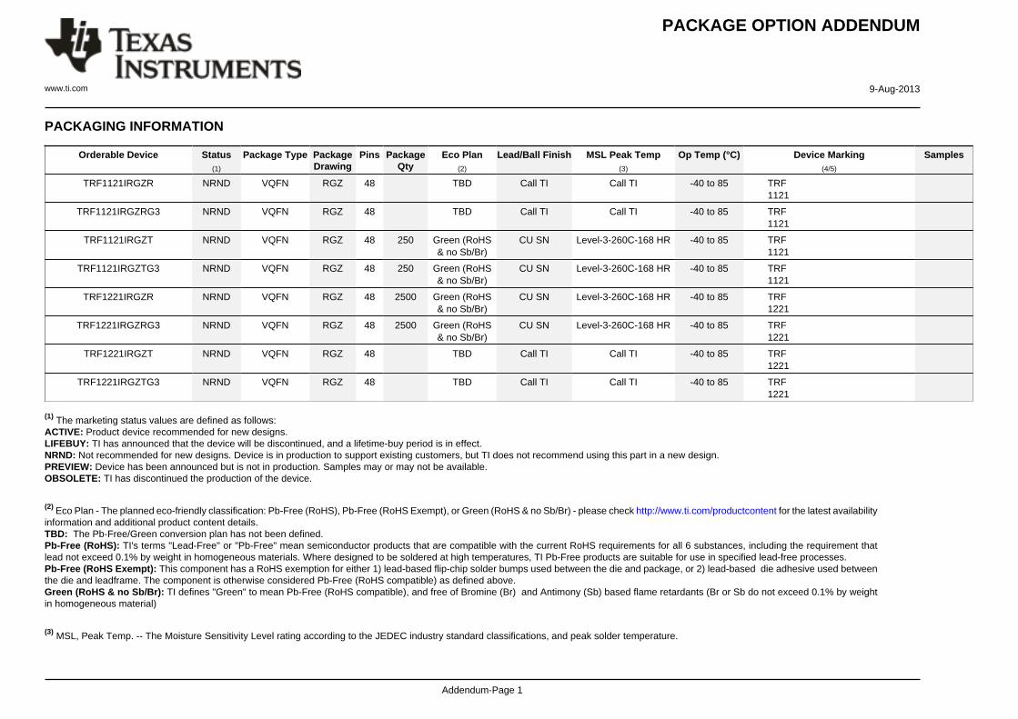
PACKAGING INFORMATION
Orderable Device Status(1)
Package Type PackageDrawing
Pins PackageQty
Eco Plan(2)
Lead/Ball Finish MSL Peak Temp(3)
Op Temp (°C) Device Marking(4/5)
Samples
TRF1121IRGZR NRND VQFN RGZ 48 TBD Call TI Call TI -40 to 85 TRF1121
TRF1121IRGZRG3 NRND VQFN RGZ 48 TBD Call TI Call TI -40 to 85 TRF1121
TRF1121IRGZT NRND VQFN RGZ 48 250 Green (RoHS& no Sb/Br)
CU SN Level-3-260C-168 HR -40 to 85 TRF1121
TRF1121IRGZTG3 NRND VQFN RGZ 48 250 Green (RoHS& no Sb/Br)
CU SN Level-3-260C-168 HR -40 to 85 TRF1121
TRF1221IRGZR NRND VQFN RGZ 48 2500 Green (RoHS& no Sb/Br)
CU SN Level-3-260C-168 HR -40 to 85 TRF1221
TRF1221IRGZRG3 NRND VQFN RGZ 48 2500 Green (RoHS& no Sb/Br)
CU SN Level-3-260C-168 HR -40 to 85 TRF1221
TRF1221IRGZT NRND VQFN RGZ 48 TBD Call TI Call TI -40 to 85 TRF1221
TRF1221IRGZTG3 NRND VQFN RGZ 48 TBD Call TI Call TI -40 to 85 TRF1221
(1) The marketing status values are defined as follows:ACTIVE: Product device recommended for new designs.LIFEBUY: TI has announced that the device will be discontinued, and a lifetime-buy period is in effect.NRND: Not recommended for new designs. Device is in production to support existing customers, but TI does not recommend using this part in a new design.PREVIEW: Device has been announced but is not in production. Samples may or may not be available.OBSOLETE: TI has discontinued the production of the device.
(2) Eco Plan - The planned eco-friendly classification: Pb-Free (RoHS), Pb-Free (RoHS Exempt), or Green (RoHS & no Sb/Br) - please check http://www.ti.com/productcontent for the latest availabilityinformation and additional product content details.TBD: The Pb-Free/Green conversion plan has not been defined.Pb-Free (RoHS): TI's terms "Lead-Free" or "Pb-Free" mean semiconductor products that are compatible with the current RoHS requirements for all 6 substances, including the requirement thatlead not exceed 0.1% by weight in homogeneous materials. Where designed to be soldered at high temperatures, TI Pb-Free products are suitable for use in specified lead-free processes.Pb-Free (RoHS Exempt): This component has a RoHS exemption for either 1) lead-based flip-chip solder bumps used between the die and package, or 2) lead-based die adhesive used betweenthe die and leadframe. The component is otherwise considered Pb-Free (RoHS compatible) as defined above.Green (RoHS & no Sb/Br): TI defines "Green" to mean Pb-Free (RoHS compatible), and free of Bromine (Br) and Antimony (Sb) based flame retardants (Br or Sb do not exceed 0.1% by weightin homogeneous material)
(3) MSL, Peak Temp. -- The Moisture Sensitivity Level rating according to the JEDEC industry standard classifications, and peak solder temperature.
PACKAGE OPTION ADDENDUM
www.ti.com 9-Aug-2013
Addendum-Page 2
(4) There may be additional marking, which relates to the logo, the lot trace code information, or the environmental category on the device.
(5) Multiple Device Markings will be inside parentheses. Only one Device Marking contained in parentheses and separated by a "~" will appear on a device. If a line is indented then it is a continuationof the previous line and the two combined represent the entire Device Marking for that device.
Important Information and Disclaimer:The information provided on this page represents TI's knowledge and belief as of the date that it is provided. TI bases its knowledge and belief on informationprovided by third parties, and makes no representation or warranty as to the accuracy of such information. Efforts are underway to better integrate information from third parties. TI has taken andcontinues to take reasonable steps to provide representative and accurate information but may not have conducted destructive testing or chemical analysis on incoming materials and chemicals.TI and TI suppliers consider certain information to be proprietary, and thus CAS numbers and other limited information may not be available for release.
In no event shall TI's liability arising out of such information exceed the total purchase price of the TI part(s) at issue in this document sold by TI to Customer on an annual basis.
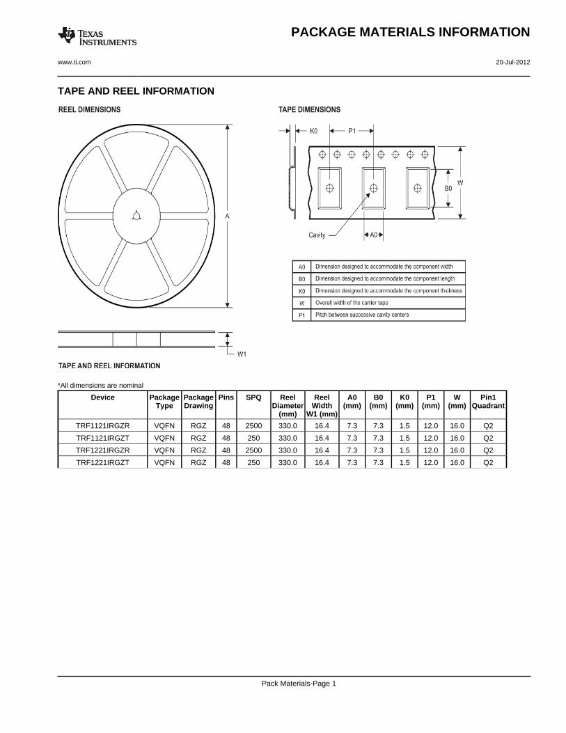
TAPE AND REEL INFORMATION
*All dimensions are nominal
Device PackageType
PackageDrawing
Pins SPQ ReelDiameter
(mm)
ReelWidth
W1 (mm)
A0(mm)
B0(mm)
K0(mm)
P1(mm)
W(mm)
Pin1Quadrant
TRF1121IRGZR VQFN RGZ 48 2500 330.0 16.4 7.3 7.3 1.5 12.0 16.0 Q2
TRF1121IRGZT VQFN RGZ 48 250 330.0 16.4 7.3 7.3 1.5 12.0 16.0 Q2
TRF1221IRGZR VQFN RGZ 48 2500 330.0 16.4 7.3 7.3 1.5 12.0 16.0 Q2
TRF1221IRGZT VQFN RGZ 48 250 330.0 16.4 7.3 7.3 1.5 12.0 16.0 Q2
PACKAGE MATERIALS INFORMATION
www.ti.com 20-Jul-2012
Pack Materials-Page 1
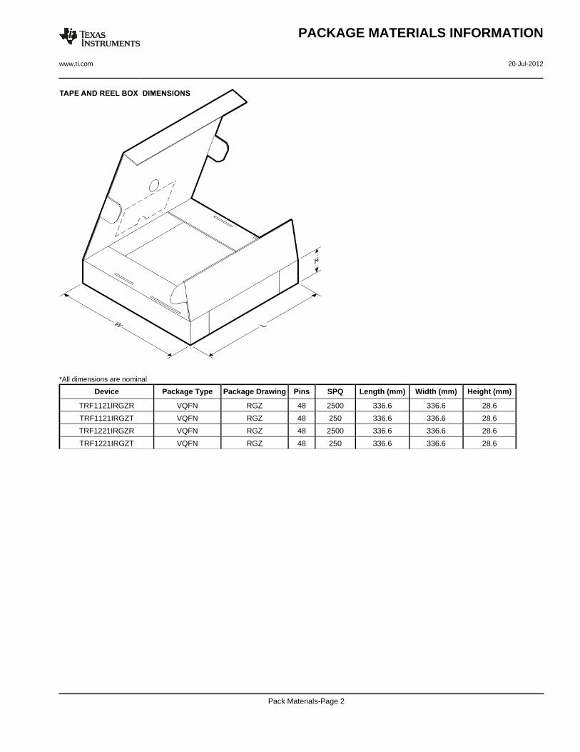
*All dimensions are nominal
Device Package Type Package Drawing Pins SPQ Length (mm) Width (mm) Height (mm)
TRF1121IRGZR VQFN RGZ 48 2500 336.6 336.6 28.6
TRF1121IRGZT VQFN RGZ 48 250 336.6 336.6 28.6
TRF1221IRGZR VQFN RGZ 48 2500 336.6 336.6 28.6
TRF1221IRGZT VQFN RGZ 48 250 336.6 336.6 28.6
PACKAGE MATERIALS INFORMATION
www.ti.com 20-Jul-2012
Pack Materials-Page 2
IMPORTANT NOTICE
Texas Instruments Incorporated and its subsidiaries (TI) reserve the right to make corrections, enhancements, improvements and otherchanges to its semiconductor products and services per JESD46, latest issue, and to discontinue any product or service per JESD48, latestissue. Buyers should obtain the latest relevant information before placing orders and should verify that such information is current andcomplete. All semiconductor products (also referred to herein as “components”) are sold subject to TI’s terms and conditions of salesupplied at the time of order acknowledgment.
TI warrants performance of its components to the specifications applicable at the time of sale, in accordance with the warranty in TI’s termsand conditions of sale of semiconductor products. Testing and other quality control techniques are used to the extent TI deems necessaryto support this warranty. Except where mandated by applicable law, testing of all parameters of each component is not necessarilyperformed.
TI assumes no liability for applications assistance or the design of Buyers’ products. Buyers are responsible for their products andapplications using TI components. To minimize the risks associated with Buyers’ products and applications, Buyers should provideadequate design and operating safeguards.
TI does not warrant or represent that any license, either express or implied, is granted under any patent right, copyright, mask work right, orother intellectual property right relating to any combination, machine, or process in which TI components or services are used. Informationpublished by TI regarding third-party products or services does not constitute a license to use such products or services or a warranty orendorsement thereof. Use of such information may require a license from a third party under the patents or other intellectual property of thethird party, or a license from TI under the patents or other intellectual property of TI.
Reproduction of significant portions of TI information in TI data books or data sheets is permissible only if reproduction is without alterationand is accompanied by all associated warranties, conditions, limitations, and notices. TI is not responsible or liable for such altereddocumentation. Information of third parties may be subject to additional restrictions.
Resale of TI components or services with statements different from or beyond the parameters stated by TI for that component or servicevoids all express and any implied warranties for the associated TI component or service and is an unfair and deceptive business practice.TI is not responsible or liable for any such statements.
Buyer acknowledges and agrees that it is solely responsible for compliance with all legal, regulatory and safety-related requirementsconcerning its products, and any use of TI components in its applications, notwithstanding any applications-related information or supportthat may be provided by TI. Buyer represents and agrees that it has all the necessary expertise to create and implement safeguards whichanticipate dangerous consequences of failures, monitor failures and their consequences, lessen the likelihood of failures that might causeharm and take appropriate remedial actions. Buyer will fully indemnify TI and its representatives against any damages arising out of the useof any TI components in safety-critical applications.
In some cases, TI components may be promoted specifically to facilitate safety-related applications. With such components, TI’s goal is tohelp enable customers to design and create their own end-product solutions that meet applicable functional safety standards andrequirements. Nonetheless, such components are subject to these terms.
No TI components are authorized for use in FDA Class III (or similar life-critical medical equipment) unless authorized officers of the partieshave executed a special agreement specifically governing such use.
Only those TI components which TI has specifically designated as military grade or “enhanced plastic” are designed and intended for use inmilitary/aerospace applications or environments. Buyer acknowledges and agrees that any military or aerospace use of TI componentswhich have not been so designated is solely at the Buyer's risk, and that Buyer is solely responsible for compliance with all legal andregulatory requirements in connection with such use.
TI has specifically designated certain components as meeting ISO/TS16949 requirements, mainly for automotive use. In any case of use ofnon-designated products, TI will not be responsible for any failure to meet ISO/TS16949.
Products Applications
Audio www.ti.com/audio Automotive and Transportation www.ti.com/automotive
Amplifiers amplifier.ti.com Communications and Telecom www.ti.com/communications
Data Converters dataconverter.ti.com Computers and Peripherals www.ti.com/computers
DLP® Products www.dlp.com Consumer Electronics www.ti.com/consumer-apps
DSP dsp.ti.com Energy and Lighting www.ti.com/energy
Clocks and Timers www.ti.com/clocks Industrial www.ti.com/industrial
Interface interface.ti.com Medical www.ti.com/medical
Logic logic.ti.com Security www.ti.com/security
Power Mgmt power.ti.com Space, Avionics and Defense www.ti.com/space-avionics-defense
Microcontrollers microcontroller.ti.com Video and Imaging www.ti.com/video
RFID www.ti-rfid.com
OMAP Applications Processors www.ti.com/omap TI E2E Community e2e.ti.com
Wireless Connectivity www.ti.com/wirelessconnectivity
Mailing Address: Texas Instruments, Post Office Box 655303, Dallas, Texas 75265Copyright © 2013, Texas Instruments Incorporated