Dual universal asynchronous receiver/transmitter … universal asynchronous receiver/transmitter ......
31
Philips Semiconductors SC26C92 Dual universal asynchronous receiver/transmitter (DUART) Product specification Supersedes data of 1998 Nov 09 IC19 Data Handbook 2000 Jan 31 INTEGRATED CIRCUITS
Transcript of Dual universal asynchronous receiver/transmitter … universal asynchronous receiver/transmitter ......

SC26C92Dual universal asynchronousreceiver/transmitter (DUART)
Product specificationSupersedes data of 1998 Nov 09IC19 Data Handbook
2000 Jan 31
INTEGRATED CIRCUITS

Philips Semiconductors Product specification
SC26C92Dual universal asynchronous receiver/transmitter (DUART)
22000 Jan 31 853–1585 23061
DESCRIPTIONThe SC26C92 is a pin and function replacement for the SCC2692and SCN2681 with added features and deeper FIFOs. Itsconfiguration on power up is that of the 2692. Its differences fromthe 2692 are: 8 character receiver, 8 character transmit FIFOs,watch dog timer for each receiver, mode register 0 is added,extended baud rate and overall faster speeds, programmablereceiver and transmitter interrupts. (The SCC2692 is not beingdiscontinued.)
The Philips Semiconductors SC26C92 Dual UniversalAsynchronous Receiver/Transmitter (DUART) is a single-chipCMOS-LSI communications device that provides two full-duplexasynchronous receiver/transmitter channels in a single package. Itinterfaces directly with microprocessors and may be used in a polledor interrupt driven system and provides modem and DMA interface.
The operating mode and data format of each channel can beprogrammed independently. Additionally, each receiver andtransmitter can select its operating speed as one of 27 fixed baudrates, a 16X clock derived from a programmable counter/timer, or anexternal 1X or 16X clock. The baud rate generator andcounter/timer can operate directly from a crystal or from externalclock inputs. The ability to independently program the operatingspeed of the receiver and transmitter make the DUART particularlyattractive for dual-speed channel applications such as clusteredterminal systems.
Each receiver and transmitter is buffered by eight character FIFOsto minimize the potential of receiver overrun, transmitter underrunand to reduce interrupt overhead in interrupt driven systems. Inaddition, a flow control capability is provided via RTS/CTS signalingto disable a remote transmitter when the receiver buffer is full.
Also provided on the SC26C92 are a multipurpose 7-bit input portand a multipurpose 8-bit output port. These can be used as generalpurpose I/O ports or can be assigned specific functions (such asclock inputs or status/interrupt outputs) under program control.
The SC26C92 is available in three package versions: 40-pin 0.6”wide DIP, a 44-pin PLCC and 44–pin plastic quad flat pack (PQFP).
FEATURES• Dual full-duplex independent asynchronous receiver/transmitters
• 8 character FIFOs for each receiver and transmitter
• Programmable data format
– 5 to 8 data bits plus parity
– Odd, even, no parity or force parity
– 1, 1.5 or 2 stop bits programmable in 1/16-bit increments
• 16-bit programmable Counter/Timer
• Programmable baud rate for each receiver and transmitterselectable from:
– 27 fixed rates: 50 to 230.4k baud
– Other baud rates to 230.4k baud at 16X
– Programmable user-defined rates derived from aprogrammable counter/timer
– External 1X or 16X clock
• Parity, framing, and overrun error detection
• False start bit detection
• Line break detection and generation
• Programmable channel mode
– Normal (full-duplex)
– Automatic echo
– Local loopback
– Remote loopback
– Multidrop mode (also called ‘wake-up’ or ‘9-bit’)
• Multi-function 7-bit input port
– Can serve as clock, modem, or control inputs
– Change of state detection on four inputs
– Inputs have typically >100k pull-up resistors
• Multi-function 8-bit output port
– Individual bit set/reset capability
– Outputs can be programmed to be status/interrupt signals
– FIFO states for DMA and modem interface
• Versatile interrupt system
– Single interrupt output with eight maskable interruptingconditions
– Output port can be configured to provide a total of up to sixseparate wire-ORable interrupt outputs
– Each FIFO can be programmed for four different interrupt levels
– Watch dog timer for each receiver
• Maximum data transfer rates:1X – 1Mb/sec, 16X – 1Mb/sec
• Automatic wake-up mode for multidrop applications
• Start-end break interrupt/status
• Detects break which originates in the middle of a character
• On-chip crystal oscillator
• Power down mode
• Receiver timeout mode
• Single +5V power supply
• Powers up to emulate SCC2692
ORDERING INFORMATION
DESCRIPTIONCOMMERCIAL1 INDUSTRIAL
DWG #DESCRIPTIONVCC = +5V ±10%, TA = 0 to +70°C VCC = +5V ±10%, TA = -40 to +85°C
DWG #
40-Pin Plastic Dual In-Line Package (DIP) SC26C92C1N SC26C92A1N SOT129-1
44-Pin Plastic Leaded Chip Carrier (PLCC) SC26C92C1A SC26C92A1A SOT187-2
44–Pin Plastic Quad Flat Pack (PQFP) SC26C92C1B SC26C92A1B SOT307–2

Philips Semiconductors Product specification
SC26C92Dual universal asynchronous receiver/transmitter (DUART)
2000 Jan 31 3
NOTE:1. Commercial devices are tested for the –40 to +85C.
PIN CONFIGURATIONS
PIN/FUNCTION PIN/FUNCTION 1 NC 23 NC 2 A0 24 INTRN 3 IP3 25 D6 4 A1 26 D4 5 IP1 27 D2 6 A2 28 D0 7 A3 29 OP6 8 IP0 30 OP4 9 WRN 31 OP210 RDN 32 OP011 RXDB 33 TXDA12 NC 34 NC13 TXDB 35 RXDA14 OP1 36 X1/CLK15 OP3 37 X216 OP5 38 RESET17 OP7 39 CEN18 D1 40 IP219 D3 41 IP620 D5 42 IP521 D7 43 IP422 VSS 44 VCC
SD00667
24
23
22
2120
19
18
17
16
15
28
27
12
10
11
9
8
7
6
5
4
3
2
1
14
13
26
25
29
30
31
32
33
34
35
36
37
38
39
40
DIP
VCC
IP4
IP5
IP6
IP2
CEN
RESET
X2
X1/CLK
RxDA
TxDA
OP0
OP2
OP4
OP6
D0
D2
D4
D6
INTRN
A0
IP3
A1
IP1
A2
A3
IP0
WRN
RDN
RxDB
TxDB
OP1
OP3
OP5
OP7
D1
D3
D5
D7
VSS
1
39
17
28
40
29
18
7
PLCC
6
TOP VIEW
INDEXCORNER
PIN/FUNCTION PIN/FUNCTION 1 A3 23 N/C 2 IP0 24 OP6 3 WRN 25 OP4 4 RDN 26 OP2 5 RxDB 27 OP0 6 TxDB 28 TxDA 7 OP1 29 RxDA 8 OP3 30 X1/CLK 9 OP5 31 X210 OP7 32 RESET11 N/C 33 CEN12 D1 34 IP213 D3 35 IP614 D5 36 IP515 D7 37 IP416 GND 38 VCC17 GND 39 VCC18 INTRN 40 A019 D6 41 IP320 D4 42 A121 D2 43 IP122 D0 44 A2
33
11
22
34
23
12
1
PQFP
44
TOP VIEW
Figure 1. Pin Configurations

Philips Semiconductors Product specification
SC26C92Dual universal asynchronous receiver/transmitter (DUART)
2000 Jan 31 4
BLOCK DIAGRAM
8
D0–D7
RDN
WRN
CEN
A0–A3
RESET
INTRN
X1/CLK
X2
4
BUS BUFFER
OPERATION CONTROL
ADDRESSDECODE
R/W CONTROL
INTERRUPT CONTROL
IMR
ISR
TIMING
BAUD RATEGENERATOR
CLOCKSELECTORS
COUNTER/TIMER
XTAL OSC
CSRA
CSRB
ACR
CTPL
CHANNEL A
8 BYTE TRANSMITFIFO
TRANSMITSHIFT REGISTER
8 BYTE RECEIVEFIFO
MRA0, 1, 2
CRA
SRA
INPUT PORT
CHANGE OFSTATE
DETECTORS (4)
OUTPUT PORT
FUNCTIONSELECT LOGIC
OPCR
TxDA
RxDA
IP0-IP6
OP0-OP7
VCC
VSS
CO
NT
RO
L
TIM
ING
INT
ER
NA
L D
ATA
BU
SCHANNEL B(AS ABOVE)
IPCR
ACR
OPR
CTPL
U
RxDB
TxDB
8
7
WATCH DOG TIMER
RECEIVE SHIFTREGISTER
SD00153
Figure 2. Block Diagram
Philips Semiconductors Product specification
SC26C92Dual universal asynchronous receiver/transmitter (DUART)
2000 Jan 31 5
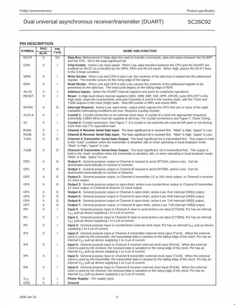
PIN DESCRIPTION
SYMBOLPKG PIN
NAME AND FUNCTIONSYMBOL 40,44 TYPE NAME AND FUNCTION
D0-D7 X I/O Data Bus: Bidirectional 3-State data bus used to transfer commands, data and status between the DUARTand the CPU. D0 is the least significant bit.
CEN X I Chip Enable: Active-Low input signal. When Low, data transfers between the CPU and the DUART areenabled on D0-D7 as controlled by the WRN, RDN and A0-A3 inputs. When High, places the D0-D7 linesin the 3-State condition.
WRN X I Write Strobe: When Low and CEN is also Low, the contents of the data bus is loaded into the addressedregister. The transfer occurs on the rising edge of the signal.
RDN X I Read Strobe: When Low and CEN is also Low, causes the contents of the addressed register to bepresented on the data bus. The read cycle begins on the falling edge of RDN.
A0-A3 X I Address Inputs: Select the DUART internal registers and ports for read/write operations.RESET X I Reset: A High level clears internal registers (SRA, SRB, IMR, ISR, OPR, OPCR), puts OP0-OP7 in the
High state, stops the counter/timer, and puts Channels A and B in the inactive state, with the TxDA andTxDB outputs in the mark (High) state. Sets MR pointer to MR1 and resets MR0.
INTRN X O Interrupt Request: Active-Low, open-drain, output which signals the CPU that one or more of the eightmaskable interrupting conditions are true. Requires a pullup resistor.
X1/CLK X I Crystal 1: Crystal connection or an external clock input. A crystal of a clock the appropriate frequency(nominally 3.6864 MHz) must be supplied at all times. For crystal connections see Figure 7, Clock Timing.
X2 X I Crystal 2: Crystal connection. See Figure 7. If a crystal is not used this pin must be left open or not drivingmore than one TTL equivalent load.
RxDA X I Channel A Receiver Serial Data Input: The least significant bit is received first. “Mark” is High, “space” is Low.RxDB X I Channel B Receiver Serial Data Input: The least significant bit is received first. “Mark” is High, “space” is Low.TxDA X O Channel A Transmitter Serial Data Output: The least significant bit is transmitted first. This output is held
in the “mark” condition when the transmitter is disabled, idle or when operating in local loopback mode.“Mark” is High, “space” is Low.
TxDB X O Channel B Transmitter Serial Data Output: The least significant bit is transmitted first. This output isheld in the ‘mark’ condition when the transmitter is disabled, idle, or when operating in local loopback mode.‘Mark’ is High, ‘space’ is Low.
OP0 X O Output 0: General purpose output or Channel A request to send (RTSAN, active-Low). Can bedeactivated automatically on receive or transmit.
OP1 X O Output 1: General purpose output or Channel B request to send (RTSBN, active-Low). Can bedeactivated automatically on receive or transmit.
OP2 X O Output 2: General purpose output, or Channel A transmitter 1X or 16X clock output, or Channel A receiver1X clock output.
OP3 X O Output 3: General purpose output or open-drain, active-Low counter/timer output or Channel B transmitter1X clock output, or Channel B receiver 1X clock output.
OP4 X O Output 4: General purpose output or Channel A open-drain, active-Low, RxA interrupt ISR[1] output.OP5 X O Output 5: General purpose output or Channel B open-drain, active-Low, RxB interrupt ISR[5] output.OP6 X O Output 6: General purpose output or Channel A open-drain, active-Low, TxA interrupt ISR[0] output.OP7 X O Output 7: General purpose output, or Channel B open-drain, active-Low, TxB interrupt ISR[4] output.IP0 X I Input 0: General purpose input or Channel A clear to send active-Low input (CTSAN). Pin has an internal
VCC pull-up device supplying 1 to 4 A of current.
IP1 X I Input 1: General purpose input or Channel B clear to send active-Low input (CTSBN). Pin has an internalVCC pull-up device supplying 1 to 4 A of current.
IP2 X I Input 2: General purpose input or counter/timer external clock input. Pin has an internal VCC pull-up devicesupplying 1 to 4 A of current.
IP3 X I Input 3: General purpose input or Channel A transmitter external clock input (TxCA). When the externalclock is used by the transmitter, the transmitted data is clocked on the falling edge of the clock. Pin has aninternal VCC pull-up device supplying 1 to 4 A of current.
IP4 X I Input 4: General purpose input or Channel A receiver external clock input (RxCA). When the externalclock is used by the receiver, the received data is sampled on the rising edge of the clock. Pin has aninternal VCC pull-up device supplying 1 to 4 A of current.
IP5 X I Input 5: General purpose input or Channel B transmitter external clock input (TxCB). When the externalclock is used by the transmitter, the transmitted data is clocked on the falling edge of the clock. Pin has aninternal VCC pull-up device supplying 1 to 4 A of current.
IP6 X I Input 6: General purpose input or Channel B receiver external clock input (RxCB). When the externalclock is used by the receiver, the received data is sampled on the rising edge of the clock. Pin has aninternal VCC pull-up device supplying 1 to 4 A of current.
VCC X I Power Supply: +5V supply input.GND X I Ground

Philips Semiconductors Product specification
SC26C92Dual universal asynchronous receiver/transmitter (DUART)
2000 Jan 31 6
ABSOLUTE MAXIMUM RATINGS 1
SYMBOL PARAMETER RATING UNIT
TA Operating ambient temperature range2 Note 4 °CTSTG Storage temperature range -65 to +150 °CVCC Voltage from VCC to GND3 -0.5 to +7.0 V
VS Voltage from any pin to GND3 -0.5 to VCC +0.5 V
PD Package power dissipation (DIP40) 2.8 W
PD Package power dissipation (PLCC44) 2.4 W
PD Package power dissipation (PQFP44) 1.78 W
Derating factor above 25C (PDIP40) 22 mW/C
Derating factor above 25C (PLCC44) 19 mW/C
Derating factor above 25C (PQFP44) 14 mW/C
NOTES:1. Stresses above those listed under Absolute Maximum Ratings may cause permanent damage to the device. This is a stress rating only and
functional operation of the device at these or any other condition above those indicated in the operation section of this specification is notimplied.
2. For operating at elevated temperatures, the device must be derated based on +150°C maximum junction temperature.3. This product includes circuitry specifically designed for the protection of its internal devices from damaging effects of excessive static
charge. Nonetheless, it is suggested that conventional precautions be taken to avoid applying any voltages larger than the rated maxima.4. Parameters are valid over specified temperature range.
DC ELECTRICAL CHARACTERISTICS 1, 2 VCC = 5V ± 10%, TA = –40C to 85C, unless otherwise specified.
LIMITS
SYMBOL PARAMETER TEST CONDITIONS Min Typ Max UNIT
VIL Input low voltage 0.8 V
VIH Input high voltage (except X1/CLK) –40 to +85°C 2.5 V
VIH Input high voltage (X1/CLK) 0.8 VCC V
VOLVOH
Output low voltageOutput high voltage (except OD outputs)3
IOL = 2.4mA
IOH = -400µA VCC -0.50.4 V
V
IIX1PDIILX1IIHX1
X1/CLK input current - power downX1/CLK input low current - operatingX1/CLK input high current - operating
VIN = 0 to VCCVIN = 0
VIN = VCC
-0.5-130
+0.5
130
µAµAµA
IIInput leakage current: All except input port pins Input port pins
VIN = 0 to VCCVIN = 0 to VCC
-0.5-8
+0.5+0.5
µAµA
IOZHIOZL
Output off current high, 3-State data busOutput off current low, 3-State data bus
VIN = VCCVIN = 0V –0.5
0.5 µAµA
IODLIODH
Open-drain output low current in off-stateOpen-drain output high current in off-state
VIN = 0VIN = VCC
–0.50.5
µAµA
ICC
Power supply current4
Operating modePower down mode5
CMOS input levelsCMOS input levels
52
1015
mAA
NOTES:1. Parameters are valid over specified temperature range.2. Typical values are at +25°C, typical supply voltages, and typical processing parameters.
3. Test conditions for outputs: CL = 150pF, except interrupt outputs. Test conditions for interrupt outputs: CL = 50pF, RL = 2.7KΩ to VCC.4. All outputs are disconnected. Inputs are switching between CMOS levels of VCC -0.2V and VSS + 0.2V.5. See UART application note for power down currents of 5µA or less.

Philips Semiconductors Product specification
SC26C92Dual universal asynchronous receiver/transmitter (DUART)
2000 Jan 31 7
AC CHARACTERISTICS 1, 2, 4
VCC = 5V ± 10%, TA = –40C to 85C, unless otherwise specified.
LIMITSSYMBOL PARAMETER Min Typ3 Max UNITReset Timing (See Figure 3)
tRES RESET pulse width 200 ns
Bus Timing 5 (See Figure 4)tAS A0-A3 setup time to RDN, WRN Low 10 nstAH A0-A3 hold time from RDN, WRN Low 25 nstCS CEN setup time to RDN, WRN Low 0 nstCH CEN hold time from RDN, WRN High 0 nstRW WRN, RDN pulse width 70 nstDD Data valid after RDN Low 55 nstDF Data bus floating after RDN High 25 nstDS Data setup time before WRN or CEN High 25 nstDH Data hold time after WRN or CEN High 0 nstRWD High time between reads and/or writes5, 6 30 ns
Port Timing 5 (See Figure 5)tPS Port input setup time before RDN Low 0 nstPH Port input hold time after RDN High 0 nstPD OPn output valid from WRN High 100 ns
Interrupt Timing (See Figure 6)INTRN (or OP3-OP7 when used as interrupts) negated from:
Read RxFIFO (RxRDY/FFULL interrupt) 100 nsWrite TxFIFO (TxRDY interrupt) 100 ns
tIR Reset command (break change interrupt) 100 nsStop C/T command (counter interrupt) 100 nsRead IPCR (input port change interrupt) 100 nsWrite IMR (clear of interrupt mask bit) 100 ns
Clock Timing (See Figure 7)tCLK X1/CLK High or Low time 50 nsfCLK X1/CLK frequency 0.1 3.6864 8 MHztCTC CTCLK (IP2) High or Low time 55 nsfCTC CTCLK (IP2) frequency 0 8 MHztRX RxC High or Low time (16X) 30 nsfRX RxC frequency (16X)
(1X)800
161
MHzMHz
tTX TxC High or Low time (16X) 30 nsfTX TxC frequency (16X)
(1X)800
161
MHzMHz
Transmitter Timing (See Figure 8)tTXD TxD output delay from TxC external clock input on IP pin 60 nstTCS Output delay from TxC low at OP pin to TxD data output 5 30 ns
Receiver Timing (See Figure 9)tRXS RxD data setup time before RxC high at external clock input on IP pin 50 nstRXH RxD data hold time after RxC high at external clock input on IP pin 50 ns
NOTES:1. Parameters are valid over specified temperature range.2. All voltage measurements are referenced to ground (GND). For testing, all inputs swing between 0.4V and 3.0V with a transition time of 5ns
maximum. For X1/CLK this swing is between 0.4V and 4.4V. All time measurements are referenced at input voltages of 0.8V and 2.0V andoutput voltages of 0.8V and 2.0V, as appropriate.
3. Typical values are at +25°C, typical supply voltages, and typical processing parameters.4. Test conditions for outputs: CL = 150pF, except interrupt outputs. Test conditions for interrupt outputs: CL = 50pF, RL = 2.7KΩ to VCC.5. Timing is illustrated and referenced to the WRN and RDN inputs. Also, CEN may be the ‘strobing’ input. CEN and RDN (also CEN and
WRN) are ORed internally. The signal asserted last initiates the cycle and the signal negated first terminates the cycle.6. If CEN is used as the ‘strobing’ input, the parameter defines the minimum High times between one CEN and the next. The RDN signal must
be negated for tRWD to guarantee that any status register changes are valid.7. Minimum frequencies are not tested but are guaranteed by design. Crystal frequencies 2 to 4 MHz.8. Clocks for 1X mode should be symmetrical.

Philips Semiconductors Product specification
SC26C92Dual universal asynchronous receiver/transmitter (DUART)
2000 Jan 31 8
Block DiagramThe SC26C92 DUART consists of the following eight major sections:data bus buffer, operation control, interrupt control, timing,communications Channels A and B, input port and output port.Refer to the Block Diagram.
Data Bus BufferThe data bus buffer provides the interface between the external andinternal data buses. It is controlled by the operation control block toallow read and write operations to take place between the controllingCPU and the DUART.
Operation ControlThe operation control logic receives operation commands from theCPU and generates appropriate signals to internal sections tocontrol device operation. It contains address decoding and read andwrite circuits to permit communications with the microprocessor viathe data bus.
Interrupt ControlA single active-Low interrupt output (INTRN) is provided which isactivated upon the occurrence of any of eight internal events.Associated with the interrupt system are the Interrupt Mask Register(IMR) and the Interrupt Status Register (ISR). The IMR can beprogrammed to select only certain conditions to cause INTRN to beasserted. The ISR can be read by the CPU to determine allcurrently active interrupting conditions.
Outputs OP3-OP7 can be programmed to provide discrete interruptoutputs for the transmitter, receivers, and counter/timer.
When OP3 to OP7 are programmed as interrupts, their outputbuffers are changed to the open drain active low configuration.These pins may be used for DMA and modem control.
TIMING CIRCUITS
Crystal ClockThe timing block consists of a crystal oscillator, a baud rategenerator, a programmable 16-bit counter/timer, and four clockselectors. The crystal oscillator operates directly from a crystalconnected across the X1/CLK and X2 inputs. If an external clock ofthe appropriate frequency is available, it may be connected toX1/CLK. The clock serves as the basic timing reference for theBaud Rate Generator (BRG), the counter/timer, and other internalcircuits. A clock signal within the limits specified in thespecifications section of this data sheet must always be supplied tothe DUART.
If an external is used instead of a crystal, X1 should be driven usinga configuration similar to the one in Figure 7.
BRGThe baud rate generator operates from the oscillator or externalclock input and is capable of generating 27 commonly used datacommunications baud rates ranging from 50 to 38.4K baud.Programming bit 0 of MR0 to a “1” gives additional baud rates to230.4kB. These will be in the 16X mode. A 3.6864MHz crystal orexternal clock must be used to get the standard baud rates. Theclock outputs from the BRG are at 16X the actual baud rate. Thecounter/timer can be used as a timer to produce a 16X clock for anyother baud rate by counting down the crystal clock or an externalclock. The four clock selectors allow the independent selection, foreach receiver and transmitter, of any of these baud rates or externaltiming signal.
Counter–Timer
The Counter/Timer is a programmable 16–bit divider that is used forgenerating miscellaneous clocks or generating timeout periods.These clocks may be used by any or all of the receivers and trans-mitters in the DUART or may be directed to an I/O pin for miscella-neous use.
Counter/Timer programming
The counter timer is a 16–bit programmable divider that operates inone of three modes: counter, timer, and time out.
• Timer mode generates a square wave.
• Counter mode generates a time delay.
• Time out mode counts time between received characters.
The C/T uses the numbers loaded into the Counter/Timer LowerRegister (CTPL) and the Counter/Timer Upper Register (CTPU) asits divisor. The counter timer is controlled with six commands: Start/Stop C/T, Read/Write Counter/Timer lower register and Read/WriteCounter/Timer upper register. These commands have slight differ-ences depending on the mode of operation. Please see the detail ofthe commands under the CTPL/CTPU register descriptions.
Baud Rate Generation with the C/T
When the timer is selected as baud rates for receiver or transmittervia the Clock Select register their output will be configured as a 16xclock. Therefore one needs to program the timer to generate aclock 16 times faster than the data rate. The formula for calculating’n’, the number loaded to the CTPU and CTPL registers, based on aparticular input clock frequency is shown below.
For the timer mode the formula is as follows:
n=Clockinputfrequency
2 16 Baudratedesired
NOTE: ‘n’ may not assume values of 0 and 1.
The frequency generated from the above formula will be at a rate 16times faster than the desired baud rate. The transmitter and receiv-er state machines include divide by 16 circuits, which provide thefinal frequency and provide various timing edges used in the qualify-ing the serial data bit stream. Often this division will result in a non–integer value: 26.3 for example. One may only program integernumbers to a digital divider. There for 26 would be chosen. If 26.7were the result of the division then 27 would be chosen. This givesa baud rate error of 0.3/26.3 or 0.3/26.7 that yields a percentageerror of 1.14% or 1.12% respectively, well within the ability of theasynchronous mode of operation. Higher input frequency to thecounter reduces the error effect of the fractional division
One should be cautious about the assumed benign effects of smallerrors since the other receiver or transmitter with which one is com-municating may also have a small error in the precise baud rate. Ina ”clean” communications environment using one start bit, eight databits and one stop bit the total difference allowed between the trans-mitter and receiver frequency is approximately 4.6%. Less thaneight data bits will increase this percentage.
Communications Channels A and BEach communications channel of the SC26C92 comprises afull-duplex asynchronous receiver/transmitter (UART). The
Philips Semiconductors Product specification
SC26C92Dual universal asynchronous receiver/transmitter (DUART)
2000 Jan 31 9
operating frequency for each receiver and transmitter can beselected independently from the baud rate generator, thecounter/timer, or from an external input.
The transmitter accepts parallel data from the CPU, converts it to aserial bit stream, inserts the appropriate start, stop, and optionalparity bits and outputs a composite serial stream of data on the TxDoutput pin.
The receiver accepts serial data on the RxD pin, converts this serialinput to parallel format, checks for start bit, stop bit, parity bit (if any),or break condition and sends an assembled character to the CPUvia the receive FIFO. Three status bits (Break Received, Framingand Parity Errors) are also FIFOed with each data character.
Input PortThe inputs to this unlatched 7-bit port can be read by the CPU byperforming a read operation at address H’D’. A High input results ina logic 1 while a Low input results in a logic 0. D7 will always readas a logic 1. The pins of this port can also serve as auxiliary inputsto certain portions of the DUART logic or modem and DMA control.
Four change-of-state detectors are provided which are associatedwith inputs IP3, IP2, IP1 and IP0. A High-to-Low or Low-to-Hightransition of these inputs, lasting longer than 25 - 50µs, will set thecorresponding bit in the input port change register. The bits arecleared when the register is read by the CPU. Any change-of-statecan also be programmed to generate an interrupt to the CPU.
The input port pulse detection circuitry uses a 38.4KHz samplingclock derived from one of the baud rate generator taps. This resultsin a sampling period of slightly more than 25µs (this assumes thatthe clock input is 3.6864MHz). The detection circuitry, in order toguarantee that a true change in level has occurred, requires twosuccessive samples at the new logic level be observed. As aconsequence, the minimum duration of the signal change is 25µs ifthe transition occurs “coincident with the first sample pulse”. The50µs time refers to the situation in which the change-of-state is “justmissed” and the first change-of-state is not detected until 25µs later.All the IP pins have a small pull-up device that will source 1 to 4 Aof current from VCC. These pins do not require pull-up devices orVCC connections if they are not used.
Output PortThe output ports are controlled from five places: the OPCR register,SOPR, ROPR, the MR registers and the command register (CR).The OPCR register controls the source of the data for the outputports OP2 through OP7. The data source for output ports OP0 andOP1 is controlled by the MR and CR registers. Normally the datasource for the OP pins is from the OPR register. The OP pin drivethe inverted level (complement) of the OPR register. Example:when the SOPR is used to set the OPR bit to a logical 1 then theassociated OP pin will drive a logical 0.
The content of the OPR register is controlled by the “Set Output PortBits Command” and the “Reset Output Bits Command”. These com-mands are at E and F, respectively. When these commands areused, action takes place only at the bit locations where ones exist.For example, a one in bit location 5 of the data word used with the“Set Output Port Bits” command will result in OPR(5) being set toone. The OP5 would then be set to zero (VSS ). Similarly, a one inbit position 5 of the data word associated with the “Reset OutputPorts Bits” command would set OPR(5) to zero and, hence, the pinOP5 to a one (Vdd).
Please note that these pins drive both high and low. However whenthey are programmed to represent interrupt type functions (such as
RxRDY) they will be switched to an open drain configuration. In thisconfiguration an external pull–up device will be required
OPERATIONTransmitterThe SC26C92 is conditioned to transmit data when the transmitter isenabled through the command register. The SC26C92 indicates tothe CPU that it is ready to accept a character by setting the TxRDYbit in the status register. This condition can be programmed togenerate an interrupt request at OP0, OP1 and INTRN. When thetransmitter is initially enabled the TxRDY and TxEMT bits will be setin the status register. When a character is loaded to the transmitFIFO the TxEMT bit will be reset. The TxEMT will not set until: 1)the transmit FIFO is empty and the transmit shift register hasfinished transmitting the stop bit of the last character written to thetransmit FIFO, or 2) the transmitter is disabled and then re–enabled.The TxRDY bit is set whenever the transmitter is enabled and theTxFIFO is not full. Data is transferred from the holding register totransmit shift register when it is idle or has completed transmissionof the previous character. Characters cannot be loaded into theTxFIFO while the transmitter is disabled.
The transmitter converts the parallel data from the CPU to a serialbit stream on the TxD output pin. It automatically sends a start bitfollowed by the programmed number of data bits, an optional paritybit, and the programmed number of stop bits. The least significantbit is sent first. Following the transmission of the stop bits, if a newcharacter is not available in the TxFIFO, the TxD output remainsHigh and the TxEMT bit in the Status Register (SR) will be set to 1.Transmission resumes and the TxEMT bit is cleared when the CPUloads a new character into the TxFIFO.
If the transmitter is disabled, it continues operating until the charac-ter currently being transmitted and any characters in the TxFIFOincluding parity and stop bit(s) have been completed.
Note the differences between the transmitter disable and the trans-mitter reset: reset stops all transmission immediately, effectivelyclears the TxFIFO and resets all status and Tx interrupt conditions.Transmitter disable clears all Tx status and interrupts BUT allowsthe Tx to complete the transmission of all data in the TxFIFO and inthe shift register. While the Tx is disabled the TxFIFO can not beloaded with data.
The transmitter can be forced to send a continuous Low condition byissuing a send break command from the command register. Thetransmitter output is returned to the normal high with a stop breakcommand.
The transmitter can be reset through a software command. If it isreset, operation ceases immediately and the transmitter must beenabled through the command register before resuming operation.
If the CTS option is enabled (MR2[4] = 1), the CTSN input at IP0 orIP1 must be low in order for the character to be transmitted. Thetransmitter will check the state of the CTS input at the beginning ofeach character transmitted. If it is found to be High, the transmitterwill delay the transmission of any following characters until the CTShas returned to the low state. CTS going high during the serializa-tion of a character will not affect that character.
Transmitter “RS485 turnaround”The transmitter can also control the RTSN outputs, OP0 or OP1 viaMR2[5]. When this mode of operation is set, the meaning of theOP0 and OP1 signal will usually be ‘end of message’. Seedescription of the MR2[5] bit for more detail.

Philips Semiconductors Product specification
SC26C92Dual universal asynchronous receiver/transmitter (DUART)
2000 Jan 31 10
This feature may be used automatically “turnaround” a transceiverwhen operating in a simplex system.
Transmitter Disable Note (W.R.T. Turnaround)When the TxEMT bit is set the sequence of instructions: enabletransmitter — load transmit holding register — disable transmitterwill often result in nothing being sent. In the condition of the TxEMTbeing set do not issue the disable until the TxRDY bit goes activeagain after the character is loaded to the TxFIFO. The data is notsent if the time between the end of loading the transmit holdingregister and the disable command is less that 3/16 bit time in the16x mode. One bit time in the 1x mode.
This is sometimes the condition when the RS485 automatic “turn-around” is enabled . It will also occur when only one character is tobe sent and it is desired to disable the transmitter immediately afterthe character is loaded.
In general, when it is desired to disable the transmitter before thelast character is sent AND the TxEMT bit is set in the status registerbe sure the TxRDY bit is active immediately before issuing thetransmitter disable instruction. (TxEMT is always set if the transmit-ter has underrun or has just been enabled), TxRDY sets at the endof the “start bit” time. It is during the start bit that the data in thetransmit holding register is transferred to the transmit shift register.
Transmitter Flow control
The transmitter may be controlled by the CTSN input when enabledby MR2(4). The CTSN input would be connected to RTSN output ofthe receiver to which it is communicating. See further description inthe MR 1 and MR2 register descriptions.
ReceiverThe SC26C92 is conditioned to receive data when enabled throughthe command register. The receiver looks for a High-to-Low(mark-to-space) transition of the start bit on the RxD input pin. If atransition is detected, the state of the RxD pin is sampled each 16Xclock for 7-1/2 clocks (16X clock mode) or at the next rising edge ofthe bit time clock (1X clock mode). If RxD is sampled High, the startbit is invalid and the search for a valid start bit begins again. If RxDis still Low, a valid start bit is assumed and the receiver continues tosample the input at one bit time intervals at the theoretical center ofthe bit, until the proper number of data bits and parity bit (if any)have been assembled, and one stop bit has been detected. Theleast significant bit is received first. The data is then transferred tothe Receive FIFO and the RxRDY bit in the SR is set to a 1. Thiscondition can be programmed to generate an interrupt at OP4 orOP5 and INTRN. If the character length is less than 8 bits, the mostsignificant unused bits in the RxFIFO are set to zero.
After the stop bit is detected, the receiver will immediately look forthe next start bit. However, if a non-zero character was receivedwithout a stop bit (framing error) and RxD remains Low for one halfof the bit period after the stop bit was sampled, then the receiveroperates as if a new start bit transition had been detected at thatpoint (one-half bit time after the stop bit was sampled).
The parity error, framing error, and overrun error (if any) are strobedinto the SR at the received character boundary, before the RxRDYstatus bit is set. If a break condition is detected (RxD is Low for theentire character including the stop bit), a character consisting of allzeros will be loaded into the RxFIFO and the received break bit inthe SR is set to 1. The RxD input must return to high for two (2)clock edges of the X1 crystal clock for the receiver to recognize theend of the break condition and begin the search for a start bit. Thiswill usually require a high time of one X1 clock period or 3 X1
edges since the clock of the controller is not synchronous tothe X1 clock.
Receiver FIFOThe RxFIFO consists of a First-In-First-Out (FIFO) stack with acapacity of eight characters. Data is loaded from the receive shiftregister into the topmost empty position of the FIFO. The RxRDY bitin the status register is set whenever one or more characters areavailable to be read, and a FFULL status bit is set if all eight stackpositions are filled with data. Either of these bits can be selected tocause an interrupt. A read of the RxFIFO outputs the data at the topof the FIFO. After the read cycle, the data FIFO and its associatedstatus bits (see below) are ‘popped’ thus emptying a FIFO positionfor new data.
Receiver Status Bits
There are five (5) status bits that are evaluated with each byte (orcharacter) received: received break, framing error, parity error, over-run error, and change of break. The first three are appended toeach byte and stored in the RxFIFO. The last two are not necessar-ily related to the byte being received or a byte that is in the RxFIFO.They are however developed by the receiver state machine.
The received break, framing error, parity error and overrun error (ifany) are strobed into the RxFIFO at the received character bound-ary, before the RxRDY status bit is set. For character mode (seebelow) status reporting the SR (Status Register) indicates the condi-tion of these bits for the character that is the next to be read from theFIFO
The ”received break” will always be associated with a zero byte inthe RxFIFO. It means that zero character was a break characterand not a zero data byte. The reception of a break condition willalways set the ”change of break” (see below) status bit in the Inter-rupt Status Register (ISR). The Change of break condition is resetby a reset error status command in the command register
Break DetectionIf a break condition is detected (RxD is Low for the entire characterincluding the stop bit), a character consisting of all zeros will beloaded into the RxFIFO and the received break bit in the SR is set to1. The change of break bit also sets in the ISR The RxD input mustreturn to high for two (2) clock edges of the X1 crystal clock for thereceiver to recognize the end of the break condition and begin thesearch for a start bit.
This will usually require a high time of one X1 clock period or 3X1 edges since the clock of the controller is not synchronousto the X1 clock.
Framing ErrorA framing error occurs when a non–zero character whose parity bit(if used) and stop; bit are zero. If RxD remains low for one half ofthe bit period after the stop bit was sampled, then the receiveroperates as if the start bit of the next character had been detected.
The parity error indicates that the receiver–generated parity was notthe same as that sent by the transmitter.
The framing, parity and received break status bits are reset whenthe associated data byte is read from the RxFIFO since these “error”conditions are attached to the byte that has the error
Overrun Error
The overrun error occurs when the RxFIFO is full, the receiver shiftregister is full, and another start bit is detected. At this moment thereceiver has 9 valid characters and the start bit of the 10th has been

Philips Semiconductors Product specification
SC26C92Dual universal asynchronous receiver/transmitter (DUART)
2000 Jan 31 11
seen. At this point the host has approximately 6/16–bit time to reada byte from the RxFIFO or the overrun condition will be set. The10th character then overruns the 9th and the 11th the 10th and so onuntil an open position in the RxFIFO is seen. (“seen” meaning atleast one byte was read from the RxFIFO.)
Overrun is cleared by a use of the “error reset” command in thecommand register.
The fundamental meaning of the overrun is that data has been lost.Data in the RxFIFO remains valid. The receiver will begin placingcharacters in the RxFIFO as soon as a position becomes vacant.
Note: Precaution must be taken when reading an overrun FIFO.There will be 8 valid characters in the receiver FIFO. There willbe one character in the receiver shift register. However it willNOT be known if more than one “over–running” character hasbeen received since the overrun bit was set. The 9 th characteris received and read as valid but it will not be known how manycharacters were lost between the two characters of the 8 th and9th reads of the RxFIFO
The ”Change of break” means that either a break has been detectedor that the break condition has been cleared. This bit is available inthe ISR. The break change bit being set in the ISR and the receivedbreak bit being set in the SR will signal the beginning of a break. Atthe termination of the break condition only the change of break inthe ISR will be set. After the break condition is detected the ter-mination of the break will only be recognized when the RxD inputhas returned to the high state for two successive edges of the 1xclock; 1/2 to 1 bit time (see above).
The receiver is disabled by reset or via CR commands. A disabledreceiver will not interrupt the host CPU under any circumstance inthe normal mode of operation. If the receiver is in the multi–drop orspecial mode, it will be partially enabled and thus may cause aninterrupt. Refer to section on Wake–Up and the register descriptionfor MR1 for more information.
Receiver Status Modes (block and character)
In addition to the data word, three status bits (parity error, framingerror, and received break) are also appended to each data characterin the FIFO (overrun is not). Status can be provided in two ways, asprogrammed by the error mode control bit in the mode register. Inthe ‘character’ mode, status is provided on a character–by–charac-ter basis; the status applies only to the character at the top of theFIFO. In the ‘block’ mode, the status provided in the SR for thesethree bits is the logical–OR of the status for all characters coming tothe top of the FIFO since the last ‘reset error’ command was issued.In either mode reading the SR does not affect the FIFO. The FIFOis ‘popped’ only when the RxFIFO is read. Therefore the statusregister should be read prior to reading the FIFO.
Receiver Flow Control
The receiver can control the deactivation of RTS. If programmed tooperate in this mode, the RTSN output will be negated when a validstart bit was received and the FIFO is full. When a FIFO positionbecomes available, the RTSN output will be re–asserted automati-cally. This feature can be used to prevent an overrun, in the receiv-er, by connecting the RTSN output to the CTSN input of thetransmitting device.
Note: The transmitter may also control the “RTSN” pin. Whenunder transmitter control the meaning is completely changed.The meaning is the transmission has ended. This signal isusually used to switch (turnaround) a bi–directional driver fromtransmit to receive.
If the receiver is disabled, the FIFO characters can be read. Howev-er, no additional characters can be received until the receiver isenabled again. If the receiver is reset, the FIFO and all of the re-ceiver status, and the corresponding output ports and interrupt arereset. No additional characters can be received until the receiver isenabled again.
Receiver Reset and DisableReceiver disable stops the receiver immediately – data beingassembled in the receiver shift register is lost. Data and status inthe FIFO is preserved and may be read. A re-enable of the receiverafter a disable will cause the receiver to begin assemblingcharacters at the next start bit detected. A receiver reset will discardthe present shift register date, reset the receiver ready bit (RxRDY),clear the status of the byte at the top of the FIFO and re-align theFIFO read/write pointers.
A ‘watchdog timer’ is associated with each receiver. Its interrupt isenabled by MR0[7]. The purpose of this timer is to alert the controlprocessor that characters are in the RxFIFO which have not beenread and/or the data stream has stopped. This situation may occurat the end of a transmission when the last few characters receivedare not sufficient to cause an interrupt.
This counter times out after 64 bit times. It is reset each time acharacter is transferred from the receiver shift register to theRxFIFO or a read of the RxFIFO is executed.
Receiver Timeout ModeIn addition to the watch dog timer described in the receiver section,the counter/timer may be used for a similar function. Itsprogrammability, of course, allows much greater precision of timeout intervals.
The timeout mode uses the received data stream to control thecounter. Each time a received character is transferred from the shiftregister to the RxFIFO, the counter is restarted. If a new characteris not received before the counter reaches zero count, the counterready bit is set, and an interrupt can be generated. This mode canbe used to indicate when data has been left in the RxFIFO for morethan the programmed time limit. Otherwise, if the receiver has beenprogrammed to interrupt the CPU when the receive FIFO is full, andthe message ends before the FIFO is full, the CPU may not knowthere is data left in the FIFO. The CTU and CTL value would beprogrammed for just over one character time, so that the CPU wouldbe interrupted as soon as it has stopped receiving continuous data.This mode can also be used to indicate when the serial line hasbeen marking for longer than the programmed time limit. In thiscase, the CPU has read all of the characters from the FIFO, but thelast character received has started the count. If there is no newdata during the programmed time interval, the counter ready bit willget set, and an interrupt can be generated.
The timeout mode is enabled by writing the appropriate command tothe command register. Writing an ‘Ax’ to CRA or CRB will invokethe timeout mode for that channel. Writing a ‘Cx’ to CRA or CRB willdisable the timeout mode. The timeout mode should only be usedby one channel at once, since it uses the C/T. If, however, thetimeout mode is enabled from both receivers, the timeout will occuronly when both receivers have stopped receiving data for thetimeout period. CTU and CTL must be loaded with a value greaterthan the normal receive character period. The timeout modedisables the regular START/STOP Counter commands and puts theC/T into counter mode under the control of the received data stream.Each time a received character is transferred from the shift registerto the RxFIFO, the C/T is stopped after 1 C/T clock, reloaded with

Philips Semiconductors Product specification
SC26C92Dual universal asynchronous receiver/transmitter (DUART)
2000 Jan 31 12
the value in CTU and CTL and then restarted on the next C/T clock.If the C/T is allowed to end the count before a new character hasbeen received, the counter ready bit, ISR[3], will be set. If IMR[3] isset, this will generate an interrupt. Receiving a character after theC/T has timed out will clear the counter ready bit, ISR[3], and theinterrupt. Invoking the ‘Set Timeout Mode On’ command, CRx = ‘Ax’,will also clear the counter ready bit and stop the counter until thenext character is received.
Time Out Mode CautionWhen operating in the special time out mode, it is possible togenerate what appears to be a “false interrupt”, i.e., an interruptwithout a cause. This may result when a time-out interrupt occursand then, BEFORE the interrupt is serviced, another character isreceived, i.e., the data stream has started again. (The interruptlatency is longer than the pause in the data stream.) In this case,when a new character has been receiver, the counter/timer will berestarted by the receiver, thereby withdrawing its interrupt. If, at thistime, the interrupt service begins for the previously seen interrupt, aread of the ISR will show the “Counter Ready” bit not set. If nothingelse is interrupting, this read of the ISR will return a x’00 character.
The CTS, RTS, CTS Enable Tx signals
CTS (Clear To Send) is usually meant to be a signal to the transmit-ter meaning that it may transmit data to the receiver. The CTS inputis on pin IP0 or IP1 for the transmitter. The CTS signal is active low;thus, it is called CTSN. RTS is usually meant to be a signal from thereceiver indicating that the receiver is ready to receive data. It isalso active low and is, thus, called RTSN. RTSN is on pin OP0 orOP1. A receiver’s RTS output will usually be connected to the CTSinput of the associated transmitter. Therefore, one could say thatRTS and CTS are different ends of the same wire!
MR2(4) is the bit that allows the transmitter to be controlled by theCTS pin ( IP0 or IP1). When this bit is set to one AND the CTSinput is driven high, the transmitter will stop sending data at the endof the present character being serialized. It is usually the RTS out-put of the receiver that will be connected to the transmitter’s CTSinput. The receiver will set RTS high when the receiver FIFO is fullAND the start bit of the ninth character is sensed. Transmissionthen stops with nine valid characters in the receiver. When MR2(4)is set to one, CTSN must be at zero for the transmitter to operate. IfMR2(4) is set to zero, the IP0 or IP1 pin will have no effect on theoperation of the transmitter.
MR1(7) is the bit that allows the receiver to control OP0 or OP1.When OP0 or OP1 is controlled by the receiver, the meaning of thatpin will be RTS. However, a point of confusion arises in that thesepins may also be controlled by the transmitter. When the transmit-ter is controlling them the meaning is not RTS at all. It is, rather, thatthe transmitter has finished sending its last data byte.
Programming the OP0 or OP1 pin to be controlled by the receiverand the transmitter at the same time is allowed, but would usually beincompatible.
RTS can also be controlled by the commands 1000 and 1001 in thecommand register. RTS is expressed at the OP0 or OP1 pin whichis still an output port. Therefore, the state of OP0 or OP1 should beset low (either by commands of the CR register or by writing to theSOPR or ROPR (Set or Reset Output Port Registers) for the receiv-er to generate the proper RTS signal. The logic at the output isbasically a NAND of the bit in OPR(0) or OPR(1) register and theRTS signal as generated by the receiver. When the RTS flow con-trol is selected via the MR1(7) bit the state of the OPR(0) or OPR(1)register is not changed. Terminating the use of “Flow Control” (via
the MR registers) will return the OP pins pin to the control of theOPR register.
Multidrop Mode (9-bit or Wake-Up)The DUART is equipped with a wake up mode for multidropapplications. This mode is selected by programming bits MR1A[4:3]or MR1B[4:3] to ‘11’ for Channels A and B, respectively. In thismode of operation, a ‘master’ station transmits an address characterfollowed by data characters for the addressed ‘slave’ station. Theslave stations, with receivers that are normally disabled, examinethe received data stream and ‘wakeup’ the CPU (by setting RxRDY)only upon receipt of an address character. The CPU compares thereceived address to its station address and enables the receiver if itwishes to receive the subsequent data characters. Upon receipt ofanother address character, the CPU may disable the receiver toinitiate the process again.
A transmitted character consists of a start bit, the programmednumber of data bits, and Address/Data (A/D) bit, and theprogrammed number of stop bits. The polarity of the transmittedA/D bit is selected by the CPU by programming bitMR1A[2]/MR1B[2]. MR1A[2]/MR1B[2] = 0 transmits a zero in theA/D bit position, which identifies the corresponding data bits as datawhile MR1A[2]/MR1B[2] = 1 transmits a one in the A/D bit position,which identifies the corresponding data bits as an address. TheCPU should program the mode register prior to loading thecorresponding data bits into the TxFIFO.
In this mode, the receiver continuously looks at the received datastream, whether it is enabled or disabled. If disabled, it sets theRxRDY status bit and loads the character into the RxFIFO if thereceived A/D bit is a one (address tag), but discards the receivedcharacter if the received A/D bit is a zero (data tag). If enabled, allreceived characters are transferred to the CPU via the RxFIFO. Ineither case, the data bits are loaded into the data FIFO while theA/D bit is loaded into the status FIFO position normally used forparity error (SRA[5] or SRB[5]). Framing error, overrun error, andbreak detect operate normally whether or not the receive is enabled.
PROGRAMMINGThe operation of the DUART is programmed by writing control wordsinto the appropriate registers. Operational feedback is provided viastatus registers which can be read by the CPU. The addressing ofthe registers is described in Table 1.
The contents of certain control registers are initialized to zero onRESET. Care should be exercised if the contents of a register arechanged during operation, since certain changes may causeoperational problems.
For example, changing the number of bits per character while thetransmitter is active may cause the transmission of an incorrectcharacter. In general, the contents of the MR, the CSR, and theOPCR should only be changed while the receiver(s) andtransmitter(s) are not enabled, and certain changes to the ACRshould only be made while the C/T is stopped.
Each channel has 3 mode registers (MR0, 1, 2) which control thebasic configuration of the channel. Access to these registers iscontrolled by independent MR address pointers. These pointers areset to 0 or 1 by MR control commands in the command register“Miscellaneous Commands”. Each time the MR registers areaccessed the MR pointer increments, stopping at MR2. It remainspointing to MR2 until set to 0 or 1 via the miscellaneous commandsof the command register. The pointer is set to 1 on reset forcompatibility with previous Philips Semiconductors UART software.

Philips Semiconductors Product specification
SC26C92Dual universal asynchronous receiver/transmitter (DUART)
2000 Jan 31 13
Mode, command, clock select, and status registers are duplicatedfor each channel to provide total independent operation and control.Refer to Table 2 for register bit descriptions. The reserved
registers at addresses H‘02’ and H‘0A’ should never be read duringnormal operation since they are reserved for internal diagnostics.
Table 1. SC26C92 Register Addressing
A3 A2 A1 A0 READ (RDN = 0) WRITE (WRN = 0)
0 0 0 0 Mode Register A (MR0A, MR1A, MR2A) Mode Register A (MR0A, MR1A, MR2A)0 0 0 1 Status Register A (SRA) Clock Select Register A (CSRA)0 0 1 0 Reserved Command Register A (CRA)0 0 1 1 Rx Holding Register A (RxFIFOA) Tx Holding Register A (TxFIFOA)0 1 0 0 Input Port Change Register (IPCR) Aux. Control Register (ACR)0 1 0 1 Interrupt Status Register (ISR) Interrupt Mask Register (IMR)0 1 1 0 Counter/Timer Upper Value (CTU) C/T Upper Preset Value (CTPU)0 1 1 1 Counter/Timer Lower Value (CTL) C/T Lower Preset Value (CTPL)1 0 0 0 Mode Register B (MR0B, MR1B, MR2B) Mode Register B (MR0B, MR1B, MR2B)1 0 0 1 Status Register B (SRB) Clock Select Register B (CSRB)1 0 1 0 Reserved Command Register B (CRB)1 0 1 1 Rx Holding Register B (RxFIFOB) Tx Holding Register B (TxFIFOB)1 1 0 0 User Defined Flag/Status Flag User Defined Flag/Status Flag1 1 0 1 Input Ports IP0 to IP6 Output Port Conf. Register (OPCR)1 1 1 0 Start Counter Command Set Output Port Bits Command (SOP12)1 1 1 1 Stop Counter Command Reset Output Port Bits Command (ROP12)
NOTE:The three MR Registers are accessed via the MR Pointer and Commands 1xh and Bxh. (Where “x” represents receiver and transmitter enable/disable control)
The following named registers are the same for ChannelsA and B
Mode Register MRnA MRnB R/W
Status Register SRA SRB R only
Clock Select CSRA CSRB W only
Command Register CRA CRB W only
Receiver FIFO RxFIFOA RxFIFOB R only
Transmitter FIFO TxFIFOA TxFIFOB W only
These registers control the functions which service bothChannels
Input Port Change Register IPCR R
Auxiliary Control Register ACR W
Interrupt Status Register ISR R
Interrupt Mask Register IMR W
Counter Timer Upper Value CTU R
Counter Timer Lower Value CTL R
Counter Timer Preset Upper CTPU W
Counter Timer Preset Lower CTPL W
Input Port Register IPR R
Output Configuration Register OPCR W
Set Output Port Bits SOPR W
Reset Output Port Bits ROPR W
Table 2. Register Bit FormatsBIT 7 BIT 6 BIT 5 BIT 4 BIT 3 BIT 2 BIT 1 BIT 0
MR0A, MR0B MR0B[3:0] are
d
Rx WATCHDOG
RxINT BIT 2 TxINT (1:0) DON’TCARE
BAUD RATEEXTENDED II
TEST 2 BAUD RATEEXTENDED 1
reservedReturns F on read
0 = Disable1 = Enable
See Tables inMR0 description
Set to 0Returns 1 on read
0 = Normal1 = Extend II
Set to 0 0 = Normal1 = Extend
BIT 7 BIT 6 BIT 5 BIT 4 BIT 3 BIT 2 BIT 1 BIT 0
MR1AMR1B
Rx CONTROLSRTS
Rx INTBIT 1
ERRORMODE PARITY MODE PARITY
TYPEBITS PER
CHARACTERMR1B0x00 0 = No
1 = Yes0 = RxRDY1 = FFULL
0 = Char1 = Block
00 = With Parity01 = Force Parity10 = No Parity11 = Multidrop Mode
0 = Even1 = Odd
00 = 501 = 610 = 711 = 8
NOTE: *In block error mode, block error conditions must be cleared by using the error reset command (command 4x) or a receiver reset.

Philips Semiconductors Product specification
SC26C92Dual universal asynchronous receiver/transmitter (DUART)
2000 Jan 31 14
BIT 7 BIT 6 BIT 5 BIT 4 BIT 3 BIT 2 BIT 1 BIT 0
MR2AMR2B
CHANNEL MODE Tx CONTROLSRTS
CTSENABLE Tx STOP BIT LENGTH*
MR2B0x00
00 = Normal01 = Auto-Echo10 = Local loop11 = Remote loop
0 = No1 = Yes
0 = No1 = Yes
0 = 0.563 4 = 0.813 8 = 1.563 C = 1.8131 = 0.625 5 = 0.875 9 = 1.625 D = 1.8752 = 0.688 6 = 0.938 A = 1.688 E = 1.9383 = 0.750 7 = 1.000 B = 1.750 F = 2.000
NOTE: *Add 0.5 to values shown for 0 – 7 if channel is programmed for 5 bits/char.
CSRA BIT 7 BIT 6 BIT 5 BIT 4 BIT 3 BIT 2 BIT 1 BIT 0CSRACSRB0 01
RECEIVER CLOCK SELECT TRANSMITTER CLOCK SELECT0x01 See Text See Text
CRABIT 7 BIT 6 BIT 5 BIT 4 BIT 3 BIT 2 BIT 1 BIT 0
CRACRB MISCELLANEOUS COMMANDS* DISABLE Tx ENABLE Tx DISABLE Rx ENABLE RxCRB0x01 See Text 0 = No
1 = Yes0 = No1 = Yes
0 = No1 = Yes
0 = No1 = Yes
NOTE: Access to the miscellaneous commands should be separated by 3 X1 clock edges. A disabled transmitter cannot be loaded.

Philips Semiconductors Product specification
SC26C92Dual universal asynchronous receiver/transmitter (DUART)
2000 Jan 31 15
Table 2. Register Bit Formats (Continued)
BIT 7 BIT 6 BIT 5 BIT 4 BIT 3 BIT 2 BIT 1 BIT 0
SRASRB0 01
RECEIVEDBREAK*
FRAMINGERROR*
PARITYERROR*
OVERRUNERROR TxEMT TxRDY FFULL RxRDY
0x01 0 = No1 = Yes
0 = No1 = Yes
0 = No1 = Yes
0 = No1 = Yes
0 = No1 = Yes
0 = No1 = Yes
0 = No1 = Yes
0 = No1 = Yes
NOTE: *These status bits are appended to the corresponding data character in the receive FIFO. A read of the status provides these bits(7:5) from the top of the FIFO together with bits (4:0). These bits are cleared by a “reset error status” command. In character mode they arediscarded when the corresponding data character is read from the FIFO. In block error mode, block error conditions must be cleared by usingthe error reset command (command 4x) or a receiver reset.
BIT 7 BIT 6 BIT 5 BIT 4 BIT 3 BIT 2 BIT 1 BIT 0
O COP7 OP6 OP5 OP4 OP3 OP2
OPCR0x0D 0 = OPR[7]
1 = TxRDYB0 = OPR[6]1 = TxRDYA
0 = OPR[5]1 = RxRDY/ FFULLB
0 = OPR[4]1 = RxRDY/ FFULLA
00 = OPR[3]01 = C/T OUTPUT10 = TxCB(1X)11 = RxCB(1X)
00 = OPR[2]01 = TxCA(16X)10 = TxCA(1X)11 = RxCA(1X)
SOPR BIT 7 BIT 6 BIT 5 BIT 4 BIT 3 BIT 2 BIT 1 BIT 00x0E See Note See Note See Note See Note See Note See Note See Note See Note
NOTE: 0 = No Change; 1 = Set
ROPR BIT 7 BIT 6 BIT 5 BIT 4 BIT 3 BIT 2 BIT 1 BIT 00x0F See Note See Note See Note See Note See Note See Note See Note See Note
NOTE: 0 = No Change; 1 = Reset
BIT 7 BIT 6 BIT 5 BIT 4 BIT 3 BIT 2 BIT 1 BIT 0
OPROP 7 OP 6 OP 5 OP 4 OP 3 OP 2 OP 1 OP 0
OPR0 = Pin High1 = Pin Low
0 = Pin High1 = Pin Low
0 = Pin High1 = Pin Low
0 = Pin High1 = Pin Low
0 = Pin High1 = Pin Low
0 = Pin High1 = Pin Low
0 = Pin High1 = Pin Low
0 = Pin High1 = Pin Low
BIT 7 BIT 6 BIT 5 BIT 4 BIT 3 BIT 2 BIT 1 BIT 0
ACR0x04
BRG SETSELECT
COUNTER/TIMERMODE AND SOURCE
DELTAIP 3 INT
DELTAIP 2 INT
DELTAIP 1 INT
DELTAIP 0 INT0x04
0 = set 11 = set 2 See Table 6 0 = Off
1 = On0 = Off1 = On
0 = Off1 = On
0 = Off1 = On
BIT 7 BIT 6 BIT 5 BIT 4 BIT 3 BIT 2 BIT 1 BIT 0
IPCR0x04
DELTAIP 3
DELTAIP 2
DELTAIP 1
DELTAIP 0 IP 3 IP 2 IP 1 IP 0
0x040 = No1 = Yes
0 = No1 = Yes
0 = No1 = Yes
0 = No1 = Yes
0 = Low1 = High
0 = Low1 = High
0 = Low1 = High
0 = Low1 = High
BIT 7 BIT 6 BIT 5 BIT 4 BIT 3 BIT 2 BIT 1 BIT 0
ISR0x05
INPUTPORT
CHANGE
DELTABREAK B
RxRDY/FFULLB TxRDYB COUNTER
READYDELTA
BREAK ARxRDY/FFULLA TxRDYA
0 = No1 = Yes
0 = No1 = Yes
0 = No1 = Yes
0 = No1 = Yes
0 = No1 = Yes
0 = No1 = Yes
0 = No1 = Yes
0 = No1 = Yes
BIT 7 BIT 6 BIT 5 BIT 4 BIT 3 BIT 2 BIT 1 BIT 0
IMR0x05
IN. PORTCHANGE
INT
DELTABREAK B
INT
RxRDY/FFULLB
INT
TxRDYBINT
COUNTERREADY
INT
DELTABREAK A
INT
RxRDY/FFULLA
INT
TxRDYAINT
0 = Off1 = On
0 = Off1 = On
0 = Off1 = On
0 = Off1 = On
0 = Off1 = On
0 = Off1 = On
0 = Off1 = On
0 = Off1 = On
Philips Semiconductors Product specification
SC26C92Dual universal asynchronous receiver/transmitter (DUART)
2000 Jan 31 16
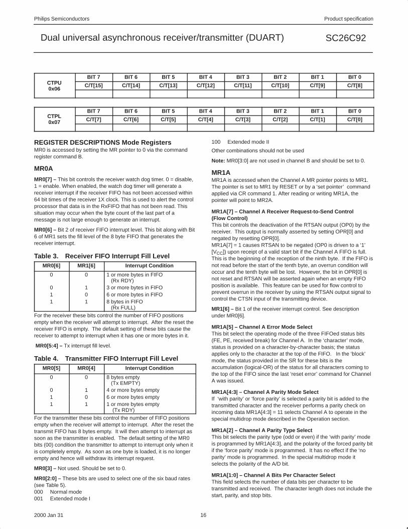
CTPUBIT 7 BIT 6 BIT 5 BIT 4 BIT 3 BIT 2 BIT 1 BIT 0
CTPU0x06
C/T[15] C/T[14] C/T[13] C/T[12] C/T[11] C/T[10] C/T[9] C/T[8]0x06
CTPLBIT 7 BIT 6 BIT 5 BIT 4 BIT 3 BIT 2 BIT 1 BIT 0
CTPL0x07 C/T[7] C/T[6] C/T[5] C/T[4] C/T[3] C/T[2] C/T[1] C/T[0]0x07
REGISTER DESCRIPTIONS Mode RegistersMR0 is accessed by setting the MR pointer to 0 via the commandregister command B.
MR0A
MR0[7] – This bit controls the receiver watch dog timer. 0 = disable,1 = enable. When enabled, the watch dog timer will generate areceiver interrupt if the receiver FIFO has not been accessed within64 bit times of the receiver 1X clock. This is used to alert the controlprocessor that data is in the RxFIFO that has not been read. Thissituation may occur when the byte count of the last part of amessage is not large enough to generate an interrupt.
MR0[6] – Bit 2 of receiver FIFO interrupt level. This bit along with Bit6 of MR1 sets the fill level of the 8 byte FIFO that generates thereceiver interrupt.
Table 3. Receiver FIFO Interrupt Fill LevelMR0[6] MR1[6] Interrupt Condition
0 0 1 or more bytes in FIFO (Rx RDY)
0 1 3 or more bytes in FIFO1 0 6 or more bytes in FIFO1 1 8 bytes in FIFO
(Rx FULL)
For the receiver these bits control the number of FIFO positionsempty when the receiver will attempt to interrupt. After the reset thereceiver FIFO is empty. The default setting of these bits cause thereceiver to attempt to interrupt when it has one or more bytes in it.
MR0[5:4] – Tx interrupt fill level.
Table 4. Transmitter FIFO Interrupt Fill LevelMR0[5] MR0[4] Interrupt Condition
0 0 8 bytes empty (Tx EMPTY)
0 1 4 or more bytes empty1 0 6 or more bytes empty1 1 1 or more bytes empty
(Tx RDY)
For the transmitter these bits control the number of FIFO positionsempty when the receiver will attempt to interrupt. After the reset thetransmit FIFO has 8 bytes empty. It will then attempt to interrupt assoon as the transmitter is enabled. The default setting of the MR0bits (00) condition the transmitter to attempt to interrupt only when itis completely empty. As soon as one byte is loaded, it is no longerempty and hence will withdraw its interrupt request.
MR0[3] – Not used. Should be set to 0.
MR0[2:0] – These bits are used to select one of the six baud rates(see Table 5).000 Normal mode001 Extended mode I
100 Extended mode II
Other combinations should not be used
Note: MR0[3:0] are not used in channel B and should be set to 0.
MR1AMR1A is accessed when the Channel A MR pointer points to MR1.The pointer is set to MR1 by RESET or by a ‘set pointer’ commandapplied via CR command 1. After reading or writing MR1A, thepointer will point to MR2A.
MR1A[7] – Channel A Receiver Request-to-Send Control(Flow Control)This bit controls the deactivation of the RTSAN output (OP0) by thereceiver. This output is normally asserted by setting OPR[0] andnegated by resetting OPR[0].MR1A[7] = 1 causes RTSAN to be negated (OP0 is driven to a ‘1’[VCC]) upon receipt of a valid start bit if the Channel A FIFO is full.This is the beginning of the reception of the ninth byte. If the FIFO isnot read before the start of the tenth byte, an overrun condition willoccur and the tenth byte will be lost. However, the bit in OPR[0] isnot reset and RTSAN will be asserted again when an empty FIFOposition is available. This feature can be used for flow control toprevent overrun in the receiver by using the RTSAN output signal tocontrol the CTSN input of the transmitting device.
MR1[6] – Bit 1 of the receiver interrupt control. See descriptionunder MR0[6].
MR1A[5] – Channel A Error Mode SelectThis bit select the operating mode of the three FIFOed status bits(FE, PE, received break) for Channel A. In the ‘character’ mode,status is provided on a character-by-character basis; the statusapplies only to the character at the top of the FIFO. In the ‘block’mode, the status provided in the SR for these bits is theaccumulation (logical-OR) of the status for all characters coming tothe top of the FIFO since the last ‘reset error’ command for ChannelA was issued.
MR1A[4:3| – Channel A Parity Mode SelectIf ‘with parity’ or ‘force parity’ is selected a parity bit is added to thetransmitted character and the receiver performs a parity check onincoming data MR1A[4:3] = 11 selects Channel A to operate in thespecial multidrop mode described in the Operation section.
MR1A[2] – Channel A Parity Type SelectThis bit selects the parity type (odd or even) if the ‘with parity’ modeis programmed by MR1A[4:3], and the polarity of the forced parity bitif the ‘force parity’ mode is programmed. It has no effect if the ‘noparity’ mode is programmed. In the special multidrop mode itselects the polarity of the A/D bit.
MR1A[1:0] – Channel A Bits Per Character SelectThis field selects the number of data bits per character to betransmitted and received. The character length does not include thestart, parity, and stop bits.

Philips Semiconductors Product specification
SC26C92Dual universal asynchronous receiver/transmitter (DUART)
2000 Jan 31 17
MR2A – Channel A Mode Register 2MR2A is accessed when the Channel A MR pointer points to MR2,which occurs after any access to MR1A. Accesses to MR2A do notchange the pointer.
MR2A[7:6] – Channel A Mode SelectEach channel of the DUART can operate in one of four modes.MR2A[7:6] = 00 is the normal mode, with the transmitter andreceiver operating independently.MR2A[7:6] = 01 places the channel in the automatic echo mode,which automatically retransmits the received data. The followingconditions are true while in automatic echo mode:1. Received data is reclocked and retransmitted on the TxDA out-
put.
2. The receive clock is used for the transmitter. Data is received onthe rising edge of the RxC1x clock and retransmitted on the nextfall of the RxC!x clock.
3. The receiver must be enabled, but the transmitter need not beenabled.
4. The Channel A TxRDY and TxEMT status bits are inactive.
5. The received parity is checked, but is not regenerated for trans-mission, i.e. transmitted parity bit is as received.
6. Character framing is checked, but the stop bits are retransmittedas received.
7. A received break is echoed as received until the next valid startbit is detected.
8. CPU to receiver communication continues normally, but the CPUto transmitter link is disabled.
MR2A(7:6) = 10 selects the local loop back diagnostic mode. In thismode:1. The transmitter output is internally connected to the receiver
input.
2. The transmit clock is used for the receiver.
3. The TxDA output is held High.
4. The RxDA input is ignored.
5. The transmitter must be enabled, but the receiver need not beenabled.
6. CPU to transmitter and receiver communications continue nor-mally.
MR2A[7:6] = 11 selects a remote loop back diagnostic mode. In thismode:1. Received data is reclocked and retransmitted on the TxDA out-
put.
2. The receive clock is used for the transmitter.
3. Received data is not sent to the local CPU, and the error statusconditions are inactive.
4. The received parity is not checked and is not regenerated fortransmission, i.e., transmitted parity is as received.
5. The receiver must be enabled.
6. Character framing is not checked, and the stop bits are retrans-mitted as received.
7. A received break is echoed as received until the next valid startbit is detected.
8. A delay of one bit time is seen at the remote receiver.
The user must exercise care when switching into and out of thevarious modes. The selected mode will be activated immediatelyupon mode selection, even if this occurs in the middle of a receivedor transmitted character. Likewise, if a mode is deselected thedevice will switch out of the mode immediately. An exception to thisis switching out of autoecho or remote loopback modes: if thede-selection occurs just after the receiver has sampled the stop bit(indicated in autoecho by assertion of RxRDY), and the transmitteris enabled, the transmitter will remain in autoecho mode until theentire stop has been re-transmitted.
MR2A[5] – Channel A Transmitter Request-to-Send ControlThis bit controls the deactivation of the RTSAN output (OP0) by thetransmitter. This output is normally asserted by setting OPR[0] andnegated by resetting OPR[0].
MR2A[5] = 1 caused OPR[0] to be reset automatically one bit timeafter the characters in the Channel A transmit shift register and inthe TxFIFO, if any, are completely transmitted including theprogrammed number of stop bits. If the transmitter is not enabled,this feature can be used to automatically terminate the transmissionof a message as follows:1. Program auto-reset mode: MR2A[5] = 1.
2. Enable transmitter.
3. Asset RTSAN: OPR[0] = 1.
4. Send message.
5. Disable transmitter after the last character is loaded into theChannel A TxFIFO. Tx status and Tx interrupts will be disabledat this time.
6. The last character will be transmitted and OPR[0] will be resetone bit time after the last stop bit, causing RTSAN to be negated.In this mode, the meaning of “RTSAN” is that the transmission isended.
MR2A[4] – Channel A Clear-to-Send ControlIf this bit is 0, CTSAN has no effect on the transmitter. If this bit is a1, the transmitter checks the state of CTSAN (IPO) each time it isready to send a character. If IPO is asserted (Low), the character istransmitted. If it is negated (High), the TxDA output remains in themarking state and the transmission is delayed until CTSAN goeslow. Changes in CTSAN while a character is being transmitted donot affect the transmission of that character..
MR2A[3:0] – Channel A Stop Bit Length SelectThis field programs the length of the stop bit appended to thetransmitted character. Stop bit lengths of 9/16 to 1 and 1-9/16 to 2bits, in increments of 1/16 bit, can be programmed for characterlengths of 6, 7, and 8 bits. For a character lengths of 5 bits, 1-1/16to 2 stop bits can be programmed in increments of 1/16 bit. In allcases, the receiver only checks for a ‘mark’ condition at the centerof the stop bit position (one–half bit time after the last data bit, orafter the parity bit if enabled is sampled).
If an external 1X clock is used for the transmitter, MR2A[3] = 0selects one stop bit and MR2A[3] = 1 selects two stop bits to betransmitted.
MR0B – Channel B Mode Register 0MR0B is accessed when the Channel B MR pointer points to MR1.The pointer is set to MR0 by RESET or by a ‘set pointer’ command

Philips Semiconductors Product specification
SC26C92Dual universal asynchronous receiver/transmitter (DUART)
2000 Jan 31 18
applied via CRB. After reading or writing MR0B, the pointer willpoint to MR1B.
The bit definitions for this register are identical to MR0A, except thatall control actions apply to the Channel B receiver and transmitterand the corresponding inputs and outputs. MR0B[3:0] are reserved.
MR1B – Channel B Mode Register 1
MR1B is accessed when the Channel B MR pointer points to MR1.The pointer is set to MR1 by RESET or by a ‘set pointer’ commandapplied via CRB. After reading or writing MR1B, the pointer willpoint to MR2B.
The bit definitions for this register are identical to MR1A, except thatall control actions apply to the Channel B receiver and transmitterand the corresponding inputs and outputs.
MR2B – Channel B Mode Register 2MR2B is accessed when the Channel B MR pointer points to MR2,which occurs after any access to MR1B. Accesses to MR2B do notchange the pointer.
The bit definitions for mode register are identical to the bitdefinitions for MR2A, except that all control actions apply to theChannel B receiver and transmitter and the corresponding inputsand outputs.
CSRA – Channel A Clock Select RegisterCSRA[7:4] – Channel A Receiver Clock SelectThis field selects the baud rate clock for the Channel A receiver.The field definition is shown in Table 5.
CSRB[7:4] ACR[7] = 0 ACR[7] = 1
11101111
IP4-16XIP4-1X
IP4-16XIP4-1X
The receiver clock is always a 16X clock except for CSRB[7:4] = 1111.
CSRA[3:0] – Channel A Transmitter Clock SelectThis field selects the baud rate clock for the Channel A transmitter.The field definition is as shown in Table 5, except as follows:
CSRA[3:0] ACR[7] = 0 ACR[7] = 1
11101111
IP3-16XIP3-1X
IP3-16XIP3-1X
The transmitter clock is always a 16X clock except for CSR[3:0] = 1111.
CSRB – Channel B Clock Select RegisterCSRB[7:4] – Channel B Receiver Clock SelectThis field selects the baud rate clock for the Channel B receiver.The field definition is as shown in Table 5, except as follows:
CSRB[7:4] ACR[7] = 0 ACR[7] = 1
11101111
IP6-16XIP6-1X
IP6-16XIP6-1X
The receiver clock is always a 16X clock except for CSRB[7:4] = 1111.
CSRB[3:0] – Channel B Transmitter Clock SelectThis field selects the baud rate clock for the Channel B transmitter.The field definition is as shown in Table 5, except as follows:
CSRB[3:0] ACR[7] = 0 ACR[7] = 1
11101111
IP5-16XIP5-1X
IP5-16XIP5-1X
The transmitter clock is always a 16X clock except forCSRB[3:0] = 1111.
Table 5. Baud Rate (Base on a 3.6864MHz crystal clock)
MR0[0] = 0 (Normal Mode) MR0[0] = 1 (Extended Mode I) MR0[2] = 1 (Extended Mode II)
CSRA[7:4] ACR[7] = 0 ACR[7] = 1 ACR[7] = 0 ACR[7] = 1 ACR[7] = 0 ACR[7] = 10000 50 75 300 450 4,800 7,2000001 110 110 110 110 880 8800010 134.5 134.5 134.5 134.5 1,076 1,0760011 200 150 1200 900 19.2K 14.4K0100 300 300 1800 1800 28.8K 28.8K0101 600 600 3600 3600 57.6K 57.6K0110 1,200 1,200 7200 7,200 115.2K 115.2K0111 1,050 2,000 1,050 2,000 1,050 2,0001000 2,400 2,400 14.4K 14.4K 57.6K 57.6K1001 4,800 4,800 28.8K 28.8K 4,800 4,8001010 7,200 1,800 7,200 1,800 57.6K 14.4K1011 9,600 9,600 57.6K 57.6K 9,600 9,6001100 38.4K 19.2K 230.4K 115.2K 38.4K 19.2K1101 Timer Timer Timer Timer Timer Timer1110 IP4-16X IP4-16X IP4-16X IP4-16X IP4-16X IP4-16X1111 IP4-1X IP4-1X IP4-1X IP4-1X IP4-1X IP4-1X
NOTE: The receiver clock is always a 16X clock except for CSRA[7:4] = 1111.

Philips Semiconductors Product specification
SC26C92Dual universal asynchronous receiver/transmitter (DUART)
2000 Jan 31 19
CRA – Channel A Command RegisterCRA is a register used to supply commands to Channel A. Multiplecommands can be specified in a single write to CRA as long as thecommands are non-conflicting, e.g., the ‘enable transmitter’ and‘reset transmitter’ commands cannot be specified in a singlecommand word.
CRA[7:4] – Miscellaneous CommandsExecution of the commands in the upper four bits of this registermust be separated by 3 X1 clock edges. Other reads or writes(including writes tot he lower four bits) may be inserted to achievethis separation.
CRA[7:4] – Command0000 No command.0001 Reset MR pointer. Causes the Channel A MR pointer to point
to MR1.0010 Reset receiver. Resets the Channel A receiver as if a
hardware reset had been applied. The receiver is disabledand the FIFO is flushed.
0011 Reset transmitter. Resets the Channel A transmitter as if ahardware reset had been applied.
0100 Reset error status. Clears the Channel A Received Break, ParityError, and Overrun Error bits in the status register (SRA[7:4]).Used in character mode to clear OE status (although RB, PEand FE bits will also be cleared) and in block mode to clear allerror status after a block of data has been received.
0101 Reset Channel A break change interrupt. Causes theChannel A break detect change bit in the interrupt statusregister (ISR[2]) to be cleared to zero.
0110 Start break. Forces the TxDA output Low (spacing). If thetransmitter is empty the start of the break condition will bedelayed up to two bit times. If the transmitter is active thebreak begins when transmission of the character iscompleted. If a character is in the TxFIFO, the start of thebreak will be delayed until that character, or any other loadedsubsequently are transmitted. The transmitter must beenabled for this command to be accepted.
0111 Stop break. The TxDA line will go High (marking) within twobit times. TxDA will remain High for one bit time before thenext character, if any, is transmitted.
1000 Assert RTSN. Causes the RTSN output to be asserted(Low).
1001 Negate RTSN. Causes the RTSN output to be negated(High).
1010 Set Timeout Mode On. The receiver in this channel willrestart the C/T as each receive character is transferred fromthe shift register to the RxFIFO. The C/T is placed in thecounter mode, the START/STOP counter commands aredisabled, the counter is stopped, and the Counter Ready Bit,ISR[3], is reset. (See also Watchdog timer description in thereceiver section.)
1011 Set MR pointer to ‘0’1100 Disable Timeout Mode. This command returns control of the
C/T to the regular START/STOP counter commands. It doesnot stop the counter, or clear any pending interrupts. Afterdisabling the timeout mode, a ‘Stop Counter’ commandshould be issued to force a reset of the ISR(3) bit.
1101 Not used.1110 Power Down Mode On. In this mode, the DUART oscillator is
stopped and all functions requiring this clock are suspended.The execution of commands other than disable power downmode (1111) requires a X1/CLK. While in the power downmode, do not issue any commands to the CR except thedisable power down mode command. The contents of allregisters will be saved while in this mode. . It isrecommended that the transmitter and receiver be disabled
prior to placing the DUART into power down mode. Thiscommand is in CRA only.
1111 Disable Power Down Mode. This command restarts theoscillator. After invoking this command, wait for the oscillatorto start up before writing further commands to the CR. Thiscommand is in CRA only. For maximum power reductioninput pins should be at VSS or VDD.
CRA[3] – Disable Channel A TransmitterThis command terminates transmitter operation and reset theTxDRY and TxEMT status bits. However, if a character is beingtransmitted or if a character is in the TxFIFO when the transmitter isdisabled, the transmission of the character(s) is completed beforeassuming the inactive state.
CRA[2] – Enable Channel A TransmitterEnables operation of the Channel A transmitter. The TxRDY andTxEMT status bits will be asserted if the transmitter is idle.
CRA[1] – Disable Channel A ReceiverThis command terminates operation of the receiver immediately – acharacter being received will be lost. The command has no effecton the receiver status bits or any other control registers. If thespecial multidrop mode is programmed, the receiver operates evenif it is disabled. See Operation section.
CRA[0] – Enable Channel A ReceiverEnables operation of the Channel A receiver. If not in the specialwakeup mode, this also forces the receiver into the search forstart-bit state.
CRB – Channel B Command RegisterCRB is a register used to supply commands to Channel B. Multiplecommands can be specified in a single write to CRB as long as thecommands are non-conflicting, e.g., the ‘enable transmitter’ and‘reset transmitter’ commands cannot be specified in a singlecommand word.
The bit definitions for this register are identical to the bit definitionsfor CRA, with the exception of commands “Ex” and “Fx” which areused for power downmode. These two commands are not used inCRB. All other control actions that apply to CRA also apply to CRB.
SRA – Channel A Status RegisterSRA[7] – Channel A Received BreakThis bit indicates that an all zero character of the programmedlength has been received without a stop bit. Only a single FIFOposition is occupied when a break is received: further entries to theFIFO are inhibited until the RxDA line returns to the marking statefor at least one-half a bit time two successive edges of the internalor external 1X clock. This will usually require a high time of oneX1 clock period or 3 X1 edges since the clock of the controlleris not synchronous to the X1 clock.
When this bit is set, the Channel A ‘change in break’ bit in the ISR(ISR[2]) is set. ISR[2] is also set when the end of the breakcondition, as defined above, is detected.
The break detect circuitry can detect breaks that originate in themiddle of a received character. However, if a break begins in themiddle of a character, it must persist until at least the end of the nextcharacter time in order for it to be detected.
This bit is reset by command 4 (0100) written to the commandregister or by receiver reset.

Philips Semiconductors Product specification
SC26C92Dual universal asynchronous receiver/transmitter (DUART)
2000 Jan 31 20
SRA[6] – Channel A Framing ErrorThis bit, when set, indicates that a stop bit was not detected (not alogical 1) when the corresponding data character in the FIFO wasreceived. The stop bit check is made in the middle of the first stopbit position.
SRA[5] – Channel A Parity ErrorThis bit is set when the ‘with parity’ or ‘force parity’ mode isprogrammed and the corresponding character in the FIFO wasreceived with incorrect parity.
In the special multidrop mode the parity error bit stores the receiveA/D (Address/Data) bit.
SRA[4] – Channel A Overrun ErrorThis bit, when set, indicates that one or more characters in thereceived data stream have been lost. It is set upon receipt of a newcharacter when the FIFO is full and a character is already in thereceive shift register waiting for an empty FIFO position. When thisoccurs, the character in the receive shift register (and its breakdetect, parity error and framing error status, if any) is lost.
This bit is cleared by a ‘reset error status’ command.
SRA[3] – Channel A Transmitter Empty (TxEMTA)This bit will be set when the transmitter underruns, i.e., both theTxEMT and TxRDY bits are set. This bit and TxRDY are set whenthe transmitter is first enabled and at any time it is re-enabled aftereither (a) reset, or (b) the transmitter has assumed the disabledstate. It is always set after transmission of the last stop bit of acharacter if no character is in the THR awaiting transmission.
It is reset when the THR is loaded by the CPU, a pendingtransmitter disable is executed, the transmitter is reset, or thetransmitter is disabled while in the underrun condition.
SRA[2] – Channel A Transmitter Ready (TxRDYA)This bit, when set, indicates that the transmit FIFO is not full andready to be loaded with another character. This bit is cleared whenthe transmit FIFO is loaded by the CPU and there are (after thisload) no more empty locations in the FIFO. It is set when acharacter is transferred to the transmit shift register. TxRDYA isreset when the transmitter is disabled and is set when thetransmitter is first enabled. Characters loaded to the TxFIFO whilethis bit is 0 will be lost. This bit has different meaning from ISR[0].
SRA[1] – Channel A FIFO Full (FFULLA)This bit is set when a character is transferred from the receive shiftregister to the receive FIFO and the transfer causes the FIFO tobecome full, i.e., all eight FIFO positions are occupied. It is resetwhen the CPU reads the receive FIFO. If a character is waiting inthe receive shift register because the FIFO is full, FFULLA will notbe reset when the CPU reads the receive FIFO. This bit hasdifferent meaning from ISR1 when MR1 6 is programmed to a ‘1’.
SRA[0] – Channel A Receiver Ready (RxRDYA)This bit indicates that a character has been received and is waitingin the FIFO to be read by the CPU. It is set when the character istransferred from the receive shift register to the FIFO and resetwhen the CPU reads the receive FIFO, only if (after this read) thereare no more characters in the FIFO. The RxFIFO becomes empty.
SRB – Channel B Status RegisterThe bit definitions for this register are identical to the bit definitionsfor SRA, except that all status applies to the Channel B receiver andtransmitter and the corresponding inputs and outputs.
OPCR – Output Port Configuration RegisterOPCR[7] – OP7 Output SelectThis bit programs the OP7 output to provide one of the following:0 The complement of OPR[7].
1 The Channel B transmitter interrupt output which is the comple-ment of ISR[4]. When in this mode OP7 acts as an open- drainoutput. Note that this output is not masked by the contents of theIMR.
OPCR[6] – OP6 Output SelectThis bit programs the OP6 output to provide one of the following:0 The complement of OPR[6].
1 The Channel A transmitter interrupt output which is the comple-ment of ISR[0]. When in this mode OP6 acts as an open- drainoutput. Note that this output is not masked by the contents of theIMR.
OPCR[5] – OP5 Output SelectThis bit programs the OP5 output to provide one of the following:0 The complement of OPR[5].
1 The Channel B receiver interrupt output which is the complementof ISR[5]. When in this mode OP5 acts as an open-drain output.Note that this output is not masked by the contents of the IMR.
OPCR[4] – OP4 Output SelectThis field programs the OP4 output to provide one of the following:0 The complement of OPR[4].
1 The Channel A receiver interrupt output which is the complementof ISR[1]. When in this mode OP4 acts as an open-drain output.Note that this output is not masked by the contents of the IMR.
OPCR[3:2] – OP3 Output SelectThis bit programs the OP3 output to provide one of the following:00 The complement of OPR[3].
01 The counter/timer output, in which case OP3 acts as an open-drain output. In the timer mode, this output is a square wave atthe programmed frequency. In the counter mode, the outputremains High until terminal count is reached, at which time itgoes Low. The output returns to the High state when the counteris stopped by a stop counter command. Note that this output isnot masked by the contents of the IMR.
10 The 1X clock for the Channel B transmitter, which is the clockthat shifts the transmitted data. If data is not being transmitted, afree running 1X clock is output.
11 The 1X clock for the Channel B receiver, which is the clock thatsamples the received data. If data is not being received, a freerunning 1X clock is output.
OPCR[1:0] – OP2 Output SelectThis field programs the OP2 output to provide one of the following:00 The complement of OPR[2].
01 The 16X clock for the Channel A transmitter. This is the clockselected by CSRA[3:0], and will be a 1X clock if CSRA[3:0] =1111.
10 The 1X clock for the Channel A transmitter, which is the clockthat shifts the transmitted data. If data is not being transmitted, afree running 1X clock is output.
11 The 1X clock for the Channel A receiver, which is the clock thatsamples the received data. If data is not being received, a freerunning 1X clock is output.

Philips Semiconductors Product specification
SC26C92Dual universal asynchronous receiver/transmitter (DUART)
2000 Jan 31 21
SOPR – Set the Output Port Bits (OPR)
SOPR[7:0] – Ones in the byte written to this register will cause thecorresponding bit positions in the OPR to set to 1. Zeros have noeffect.
ROPR – Reset Output Port Bits (OPR)
ROPR[7:0] – Ones in the byte written to the ROPR will cause thecorresponding bit positions in the OPR to set to 0. Zeros have no effect.
Table 6. Bit Rate Generator CharacteristicsCrystal or Clock = 3.6864MHz
NORMAL RATE(BAUD)
ACTUAL 16XCLOCK (kHz)
ERROR (%)
50 0.8 075 1.2 0
110 1.759 -0.069134.5 2.153 0.059150 2.4 0200 3.2 0300 4.8 0600 9.6 0
1050 16.756 -0.2601200 19.2 01800 28.8 02000 32.056 0.1752400 38.4 04800 76.8 07200 115.2 09600 153.6 0
14.4K 230.4 019.2K 307.2 028.8K 460.8 038.4K 614.4 057.6K 921.6 0
115.2K 1843.2K 0230.4K 3686.4K 0
NOTE: Duty cycle of 16X clock is 50% ± 1%.
Asynchronous UART communications can tolerate frequency errorof 4.1% to 6.7% in a “clean” communications channel. The percentof error changes as the character length changes. The abovepercentages range from 5 bits not parity to 8 bits with parity and onestop bit. The error with 8 bits no parity and one stop bit is 4.6%. If astop bit length of 9/16 is used, the error tolerance will approach 0due to a variable error of up to 1/16 bit time in receiver clock phasealignment to the start bit.
ACR – Auxiliary Control RegisterACR[7] – Baud Rate Generator Set SelectThis bit selects one of two sets of baud rates to be generated by theBRG (see Table 5).
The selected set of rates is available for use by the Channel A andB receivers and transmitters as described in CSRA and CSRB.Baud rate generator characteristics are given in Table 6.
Table 7. ACR 6:4 Field DefinitionACR6:4 MODE CLOCK SOURCE
000 Counter External (IP2)001 Counter TxCA – 1X clock of Channel A
transmitter010 Counter TxCB – 1X clock of Channel B
transmitter011 Counter Crystal or external clock
(X1/CLK) divided by 16100 Timer (square wave) External (IP2)101 Timer (square wave) External (IP2) divided by 16110 Timer (square wave) Crystal or external clock
(X1/CLK)111 Timer (square wave) Crystal or external clock
(X1/CLK) divided by 16
NOTE: The timer mode generates a squarewave.
ACR[6:4] – Counter/Timer Mode And Clock Source SelectThis field selects the operating mode of the counter/timer and itsclock source as shown in Table 7.
ACR[3:0] – IP3, IP2, IP1, IP0 Change-of-State Interrupt EnableThis field selects which bits of the input port change register (IPCR)cause the input change bit in the interrupt status register (ISR[7]) tobe set. If a bit is in the ‘on’ state the setting of the corresponding bitin the IPCR will also result in the setting of ISR[7], which results inthe generation of an interrupt output if IMR[7] = 1. If a bit is in the‘off’ state, the setting of that bit in the IPCR has no effect on ISR[7].
IPCR – Input Port Change Register
IPCR[7:4] – IP3, IP2, IP1, IP0 Change-of-StateThese bits are set when a change-of-state, as defined in the inputport section of this data sheet, occurs at the respective input pins.They are cleared when the IPCR is read by the CPU. A read of theIPCR also clears ISR[7], the input change bit in the interrupt statusregister. The setting of these bits can be programmed to generatean interrupt to the CPU.
IPCR[3:0] – IP3, IP2, IP1, IP0 Change-of-StateThese bits provide the current state of the respective inputs. Theinformation is unlatched and reflects the state of the input pins at thetime the IPCR is read.
ISR – Interrupt Status RegisterThis register provides the status of all potential interrupt sources.The contents of this register are masked by the Interrupt MaskRegister (IMR). If a bit in the ISR is a ‘1’ and the corresponding bitin the IMR is also a ‘1’, the INTRN output will be asserted (Low). Ifthe corresponding bit in the IMR is a zero, the state of the bit in theISR has no effect on the INTRN output. Note that the IMR does notmask the reading of the ISR – the true status will be providedregardless of the contents of the IMR. The contents of this register
are initialized to H‘00’ when the DUART is reset.

Philips Semiconductors Product specification
SC26C92Dual universal asynchronous receiver/transmitter (DUART)
2000 Jan 31 22
ISR[7] – Input Port Change StatusThis bit is a ‘1’ when a change-of-state has occurred at the IP0, IP1,IP2, or IP3 inputs and that event has been selected to cause aninterrupt by the programming of ACR[3:0]. The bit is cleared whenthe CPU reads the IPCR.
ISR[6] – Channel B Change In BreakThis bit, when set, indicates that the Channel B receiver hasdetected the beginning or the end of a received break. It is resetwhen the CPU issues a Channel B ‘reset break change interrupt’command.
ISR[5] – RxB InterruptThis bit indicates that the channel B receiver is interruptingaccording to the fill level programmed by the MR0 and MR1registers. This bit has a different meaning than the receiverready/full bit in the status register.
ISR[4] – TxB InterruptThis bit indicates that the channel B transmitter is interruptingaccording to the interrupt level programmed in the MR0[5:4] bits.This bit has a different meaning than the Tx RDY bit in the statusregister.
ISR[3] – Counter Ready.In the counter mode, this bit is set when the counter reachesterminal count and is reset when the counter is stopped by a stopcounter command.
In the timer mode, this bit is set once each cycle of the generatedsquare wave (every other time that the counter/timer reaches zerocount). The bit is reset by a stop counter command. The command,however, does not stop the counter/timer.
ISR[2] – Channel A Change in BreakThis bit, when set, indicates that the Channel A receiver hasdetected the beginning or the end of a received break. It is resetwhen the CPU issues a Channel A ‘reset break change interrupt’command.
ISR[1] – RxA InterruptThis bit indicates that the channel A receiver is interruptingaccording to the fill level programmed by the MR0 and MR1registers. This bit has a different meaning than the receiverready/full bit in the status register.
ISR[0] – TxA InterruptThis bit indicates that the channel A transmitter is interruptingaccording to the interrupt level programmed in the MR0[5:4] bits.This bit has a different meaning than the Tx RDY bit in the statusregister.
IMR – Interrupt Mask RegisterThe programming of this register selects which bits in the ISRcauses an interrupt output. If a bit in the ISR is a ‘1’ and thecorresponding bit in the IMR is also a ‘1’ the INTRN output will beasserted. If the corresponding bit in the IMR is a zero, the state ofthe bit in the ISR has no effect on the INTRN output. Note that theIMR does not mask the programmable interrupt outputs OP3-OP7 orthe reading of the ISR.
CTPU and CTPL – Counter/Timer RegistersThe CTPU and CTPL hold the eight MSBs and eight LSBs,respectively, of the value to be used by the counter/timer in eitherthe counter or timer modes of operation. The minimum value whichmay be loaded into the CTPU/CTPL registers is H‘0002’. Note thatthese registers are write-only and cannot be read by the CPU.
In the timer mode, the C/T generates a square wave whose period istwice the value (in C/T clock periods) of the CTPU and CTPL. Thewaveform so generated is often used for a data clock. The formulafor calculating the divisor n to load to the CTPU and CTPL for aparticular 1X data clock is shown below.
n
counter clock frequency16 x 2 x baud rate desired
Often this division will result in a non-integer number; 26.3, forexample. One can only program integer numbers in a digital divider.Therefore, 26 would be chosen. This gives a baud rate error of0.3/26.3 which is 1.14%; well within the ability asynchronous modeof operation.
If the value in CTPU and CTPL is changed, the current half-periodwill not be affected, but subsequent half periods will be. The C/T willnot be running until it receives an initial ‘Start Counter’ command(read at address A3-A0 = 1110). After this, while in timer mode, theC/T will run continuously. Receipt of a start counter command (readwith A3-A0 = 1110) causes the counter to terminate the currenttiming cycle and to begin a new cycle using the values in CTPU andCTPL.
The counter ready status bit (ISR[3]) is set once each cycle of thesquare wave. The bit is reset by a stop counter command (readwith A3-A0 = H’F’). The command however, does not stop the C/T.The generated square wave is output on OP3 if it is programmedto be the C/T output.
In the counter mode, the value C/T loaded into CTPU and CTPL bythe CPU is counted down to 0.. Counting begins upon receipt of astart counter command. Upon reaching terminal count H‘0000’, thecounter ready interrupt bit (ISR[3]) is set. The counter continuescounting past the terminal count until stopped by the CPU. If OP3 isprogrammed to be the output of the C/T, the output remains Highuntil terminal count is reached, at which time it goes Low. Theoutput returns to the High state and ISR[3] is cleared when thecounter is stopped by a stop counter command. The CPU maychange the values of CTPU and CTPL at any time, but the newcount becomes effective only on the next start counter commands.If new values have not been loaded, the previous count values arepreserved and used for the next count cycle
In the counter mode, the current value of the upper and lower 8 bitsof the counter (CTU, CTL) may be read by the CPU. It isrecommended that the counter be stopped when reading to preventpotential problems which may occur if a carry from the lower 8 bitsto the upper 8 bits occurs between the times that both halves of thecounter are read. However, note that a subsequent start countercommand will cause the counter to begin a new count cycle usingthe values in CTPU and CTPL.
When the C/T clock divided by 16 is selected, the maximum divisorbecomes 1,048,575.

Philips Semiconductors Product specification
SC26C92Dual universal asynchronous receiver/transmitter (DUART)
2000 Jan 31 23
RESETN
tRESSD00133
Figure 3. Reset Timing
A0–A3
CEN
tAS
tCS tCH
RDN
tRW tRWD
D0–D7(READ)
tDD tDF
FLOAT FLOATVALIDNOT
VALID
WDN
tRWD
VALIDD0–D7(WRITE)
tDS
tDH
tAH
SD00087
Figure 4. Bus Timing
(b) OUTPUT PINS
RDN
IP0–IP6
WRN
OP0–OP7
tPS tPH
tPD
OLD DATA NEW DATA
(a) INPUT PINS
SD00135
Figure 5. Port Timing
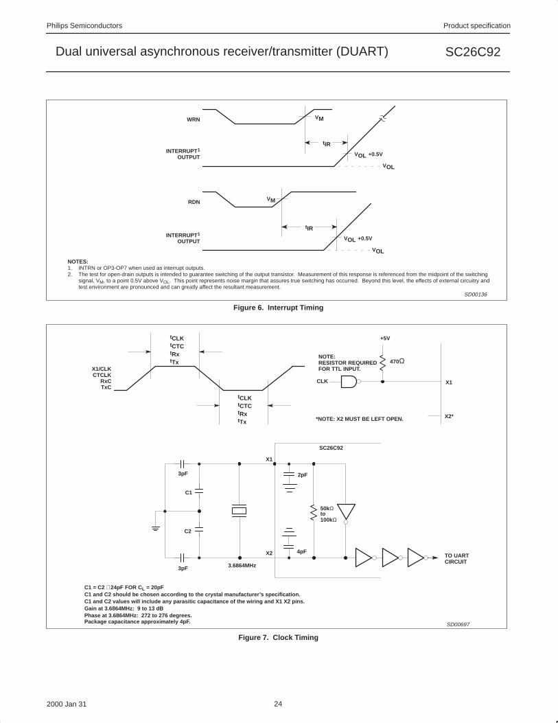
Philips Semiconductors Product specification
SC26C92Dual universal asynchronous receiver/transmitter (DUART)
2000 Jan 31 24
NOTES:1. INTRN or OP3-OP7 when used as interrupt outputs.2. The test for open-drain outputs is intended to guarantee switching of the output transistor. Measurement of this response is referenced from the midpoint of the switching
signal, VM, to a point 0.5V above VOL. This point represents noise margin that assures true switching has occurred. Beyond this level, the effects of external circuitry andtest environment are pronounced and can greatly affect the resultant measurement.
VM
VOL +0.5V
VOL
WRN
INTERRUPT1
OUTPUT
tIR
VM
VOL +0.5V
VOL
RDN
INTERRUPT1
OUTPUT
tIR
SD00136
Figure 6. Interrupt Timing
C1 = C2 ∼ 24pF FOR CL = 20pF
tCLKtCTCtRxtTx
X1/CLKCTCLK
RxCTxC
tCLKtCTCtRxtTx
+5V
470Ω
X1
X2*
CLK
*NOTE: X2 MUST BE LEFT OPEN.
X2
3.6864MHz
X1
C1
C2
SC26C92
NOTE:RESISTOR REQUIREDFOR TTL INPUT.
TO UARTCIRCUIT
50kΩto100kΩ
3pF
3pF
C1 and C2 should be chosen according to the crystal manufacturer’s specification.C1 and C2 values will include any parasitic capacitance of the wiring and X1 X2 pins.Gain at 3.6864MHz: 9 to 13 dBPhase at 3.6864MHz: 272 to 276 degrees.
2pF
4pF
Package capacitance approximately 4pF. SD00697
Figure 7. Clock Timing

Philips Semiconductors Product specification
SC26C92Dual universal asynchronous receiver/transmitter (DUART)
2000 Jan 31 25
tTXD
tTCS
1 BIT TIME(1 OR 16 CLOCKS)
TxD
TxC(INPUT)
TxC(1X OUTPUT)
SD00138
Figure 8. Transmitter External Clocks
tRXS tRXH
RxC(1X INPUT)
RxD
SD00139
Figure 9. Receiver External Clock
TRANSMITTERENABLED
TxD D1 D2 D3 D4 D6BREAK
TxRDY(SR2)
WRN
D1 D8 D9 D10 D12STARTBREAK
STOP BREAK
D11 WILLNOT BE
WRITTEN TOTHE TxFIFO
CTSN1
(IP0)
RTSN2
(OP0)
OPR(0) = 1 OPR(0) = 1NOTES:
1. Timing shown for MR2(4) = 1.
2. Timing shown for MR2(5) = 1. SD00155
Figure 10. Transmitter Timing

Philips Semiconductors Product specification
SC26C92Dual universal asynchronous receiver/transmitter (DUART)
2000 Jan 31 26
D1 D2 D8 D9 D10 D11 D12 D13RxD
D12, D13 WILL BE LOST DUE TO RECEIVER DISABLE.
RECEIVERENABLED
RxRDY(SR0)
FFULL(SR1)
RxRDY/FFULL(OP5)2
RDN
STATUS DATA
D1
STATUS DATA
D2
STATUS DATA
D3
STATUS DATA
D10D11 WILL BE LOSTDUE TO OVERRUNOVERRUN
(SR4) RESET BY COMMAND
RTS1
(OP0)
OPR(0) = 1NOTES:
1. Timing shown for MR1(7) = 1.
2. Shown for OPCR(4) = 1 and MR(6) = 0. SD00156
Figure 11. Receiver Timing
TRANSMITTERENABLED
TxD ADD#1
TxRDY(SR2)
WRN
MR1(4–3) = 11MR1(2) = 1
1
BIT 9
D0 0
BIT 9
ADD#2 1
BIT 9MASTER STATION
ADD#1 MR1(2) = 0 D0 MR1(2) = 1 ADD#2
RxD ADD#1 1
BIT 9
D0 0
BIT 9
ADD#2 1
BIT 9PERIPHERAL STATION
0
BIT 9
0
BIT 9
RECEIVERENABLED
RxRDY(SR0)
RDN/WRN
MR1(4–3) = 11 ADD#1 STATUS DATA
D0
STATUS DATA
ADD#2
SD00096
Figure 12. Wake-Up Mode

Philips Semiconductors Product specification
SC26C92Dual universal asynchronous receiver/transmitter (DUART)
2000 Jan 31 27
INTRN
D0–D7TxDA/B
OP0–OP7
50pF
+5V
2.7K
150pF
+5V
I = 2.4mA VOLI = 400µA VOH
SD00157
Figure 13. Test Conditions on Outputs

Dual universal asynchronous receiver/transmitter(DUART)
Philips Semiconductors Product specification
SC26C92
2000 Jan 31 28
DIP40: plastic dual in-line package; 40 leads (600 mil) SOT129-1

Dual universal asynchronous receiver/transmitter(DUART)
Philips Semiconductors Product specification
SC26C92
2000 Jan 31 29
PLCC44: plastic leaded chip carrier; 44 leads SOT187-2

Dual universal asynchronous receiver/transmitter(DUART)
Philips Semiconductors Product specification
SC26C92
2000 Jan 31 30
QFP44: plastic quad flat package; 44 leads (lead length 1.3 mm); body 10 x 10 x 1.75 mm SOT307-2

Dual universal asynchronous receiver/transmitter(DUART)
Philips Semiconductors Product specification
SC26C92
2000 Jan 31 31
DefinitionsShort-form specification — The data in a short-form specification is extracted from a full data sheet with the same type number and title. Fordetailed information see the relevant data sheet or data handbook.
Limiting values definition — Limiting values given are in accordance with the Absolute Maximum Rating System (IEC 134). Stress above oneor more of the limiting values may cause permanent damage to the device. These are stress ratings only and operation of the device at these orat any other conditions above those given in the Characteristics sections of the specification is not implied. Exposure to limiting values for extendedperiods may affect device reliability.
Application information — Applications that are described herein for any of these products are for illustrative purposes only. PhilipsSemiconductors make no representation or warranty that such applications will be suitable for the specified use without further testing ormodification.
DisclaimersLife support — These products are not designed for use in life support appliances, devices or systems where malfunction of these products canreasonably be expected to result in personal injury. Philips Semiconductors customers using or selling these products for use in such applicationsdo so at their own risk and agree to fully indemnify Philips Semiconductors for any damages resulting from such application.
Right to make changes — Philips Semiconductors reserves the right to make changes, without notice, in the products, including circuits, standardcells, and/or software, described or contained herein in order to improve design and/or performance. Philips Semiconductors assumes noresponsibility or liability for the use of any of these products, conveys no license or title under any patent, copyright, or mask work right to theseproducts, and makes no representations or warranties that these products are free from patent, copyright, or mask work right infringement, unlessotherwise specified.
Philips Semiconductors811 East Arques AvenueP.O. Box 3409Sunnyvale, California 94088–3409Telephone 800-234-7381
Copyright Philips Electronics North America Corporation 2000All rights reserved. Printed in U.S.A.
Date of release: 01-00
Document order number: 9397 750 06829
Data sheetstatus
Objective specification
Preliminary specification
Product specification
Productstatus
Development
Qualification
Production
Definition [1]
This data sheet contains the design target or goal specifications for product development.Specification may change in any manner without notice.
This data sheet contains preliminary data, and supplementary data will be published at a later date.Philips Semiconductors reserves the right to make changes at any time without notice in order toimprove design and supply the best possible product.
This data sheet contains final specifications. Philips Semiconductors reserves the right to makechanges at any time without notice in order to improve design and supply the best possible product.
Data sheet status
[1] Please consult the most recently issued datasheet before initiating or completing a design.